WO2022239680A1 - 光学素子 - Google Patents
光学素子 Download PDFInfo
- Publication number
- WO2022239680A1 WO2022239680A1 PCT/JP2022/019371 JP2022019371W WO2022239680A1 WO 2022239680 A1 WO2022239680 A1 WO 2022239680A1 JP 2022019371 W JP2022019371 W JP 2022019371W WO 2022239680 A1 WO2022239680 A1 WO 2022239680A1
- Authority
- WO
- WIPO (PCT)
- Prior art keywords
- potential
- transparent electrode
- liquid crystal
- axis direction
- optical element
- Prior art date
- Legal status (The legal status is an assumption and is not a legal conclusion. Google has not performed a legal analysis and makes no representation as to the accuracy of the status listed.)
- Ceased
Links
Images







Classifications
-
- G—PHYSICS
- G02—OPTICS
- G02F—OPTICAL DEVICES OR ARRANGEMENTS FOR THE CONTROL OF LIGHT BY MODIFICATION OF THE OPTICAL PROPERTIES OF THE MEDIA OF THE ELEMENTS INVOLVED THEREIN; NON-LINEAR OPTICS; FREQUENCY-CHANGING OF LIGHT; OPTICAL LOGIC ELEMENTS; OPTICAL ANALOGUE/DIGITAL CONVERTERS
- G02F1/00—Devices or arrangements for the control of the intensity, colour, phase, polarisation or direction of light arriving from an independent light source, e.g. switching, gating or modulating; Non-linear optics
- G02F1/01—Devices or arrangements for the control of the intensity, colour, phase, polarisation or direction of light arriving from an independent light source, e.g. switching, gating or modulating; Non-linear optics for the control of the intensity, phase, polarisation or colour
- G02F1/13—Devices or arrangements for the control of the intensity, colour, phase, polarisation or direction of light arriving from an independent light source, e.g. switching, gating or modulating; Non-linear optics for the control of the intensity, phase, polarisation or colour based on liquid crystals, e.g. single liquid crystal display cells
- G02F1/133—Constructional arrangements; Operation of liquid crystal cells; Circuit arrangements
- G02F1/1333—Constructional arrangements; Manufacturing methods
- G02F1/1347—Arrangement of liquid crystal layers or cells in which the final condition of one light beam is achieved by the addition of the effects of two or more layers or cells
-
- G—PHYSICS
- G02—OPTICS
- G02F—OPTICAL DEVICES OR ARRANGEMENTS FOR THE CONTROL OF LIGHT BY MODIFICATION OF THE OPTICAL PROPERTIES OF THE MEDIA OF THE ELEMENTS INVOLVED THEREIN; NON-LINEAR OPTICS; FREQUENCY-CHANGING OF LIGHT; OPTICAL LOGIC ELEMENTS; OPTICAL ANALOGUE/DIGITAL CONVERTERS
- G02F1/00—Devices or arrangements for the control of the intensity, colour, phase, polarisation or direction of light arriving from an independent light source, e.g. switching, gating or modulating; Non-linear optics
- G02F1/01—Devices or arrangements for the control of the intensity, colour, phase, polarisation or direction of light arriving from an independent light source, e.g. switching, gating or modulating; Non-linear optics for the control of the intensity, phase, polarisation or colour
- G02F1/13—Devices or arrangements for the control of the intensity, colour, phase, polarisation or direction of light arriving from an independent light source, e.g. switching, gating or modulating; Non-linear optics for the control of the intensity, phase, polarisation or colour based on liquid crystals, e.g. single liquid crystal display cells
- G02F1/133—Constructional arrangements; Operation of liquid crystal cells; Circuit arrangements
- G02F1/1333—Constructional arrangements; Manufacturing methods
- G02F1/1343—Electrodes
- G02F1/134309—Electrodes characterised by their geometrical arrangement
-
- G—PHYSICS
- G02—OPTICS
- G02F—OPTICAL DEVICES OR ARRANGEMENTS FOR THE CONTROL OF LIGHT BY MODIFICATION OF THE OPTICAL PROPERTIES OF THE MEDIA OF THE ELEMENTS INVOLVED THEREIN; NON-LINEAR OPTICS; FREQUENCY-CHANGING OF LIGHT; OPTICAL LOGIC ELEMENTS; OPTICAL ANALOGUE/DIGITAL CONVERTERS
- G02F1/00—Devices or arrangements for the control of the intensity, colour, phase, polarisation or direction of light arriving from an independent light source, e.g. switching, gating or modulating; Non-linear optics
- G02F1/01—Devices or arrangements for the control of the intensity, colour, phase, polarisation or direction of light arriving from an independent light source, e.g. switching, gating or modulating; Non-linear optics for the control of the intensity, phase, polarisation or colour
- G02F1/13—Devices or arrangements for the control of the intensity, colour, phase, polarisation or direction of light arriving from an independent light source, e.g. switching, gating or modulating; Non-linear optics for the control of the intensity, phase, polarisation or colour based on liquid crystals, e.g. single liquid crystal display cells
- G02F1/133—Constructional arrangements; Operation of liquid crystal cells; Circuit arrangements
- G02F1/1333—Constructional arrangements; Manufacturing methods
- G02F1/1343—Electrodes
-
- G—PHYSICS
- G02—OPTICS
- G02F—OPTICAL DEVICES OR ARRANGEMENTS FOR THE CONTROL OF LIGHT BY MODIFICATION OF THE OPTICAL PROPERTIES OF THE MEDIA OF THE ELEMENTS INVOLVED THEREIN; NON-LINEAR OPTICS; FREQUENCY-CHANGING OF LIGHT; OPTICAL LOGIC ELEMENTS; OPTICAL ANALOGUE/DIGITAL CONVERTERS
- G02F1/00—Devices or arrangements for the control of the intensity, colour, phase, polarisation or direction of light arriving from an independent light source, e.g. switching, gating or modulating; Non-linear optics
- G02F1/01—Devices or arrangements for the control of the intensity, colour, phase, polarisation or direction of light arriving from an independent light source, e.g. switching, gating or modulating; Non-linear optics for the control of the intensity, phase, polarisation or colour
- G02F1/13—Devices or arrangements for the control of the intensity, colour, phase, polarisation or direction of light arriving from an independent light source, e.g. switching, gating or modulating; Non-linear optics for the control of the intensity, phase, polarisation or colour based on liquid crystals, e.g. single liquid crystal display cells
- G02F1/133—Constructional arrangements; Operation of liquid crystal cells; Circuit arrangements
- G02F1/1333—Constructional arrangements; Manufacturing methods
- G02F1/1347—Arrangement of liquid crystal layers or cells in which the final condition of one light beam is achieved by the addition of the effects of two or more layers or cells
- G02F1/13471—Arrangement of liquid crystal layers or cells in which the final condition of one light beam is achieved by the addition of the effects of two or more layers or cells in which all the liquid crystal cells or layers remain transparent, e.g. FLC, ECB, DAP, HAN, TN, STN, SBE-LC cells
-
- G—PHYSICS
- G02—OPTICS
- G02F—OPTICAL DEVICES OR ARRANGEMENTS FOR THE CONTROL OF LIGHT BY MODIFICATION OF THE OPTICAL PROPERTIES OF THE MEDIA OF THE ELEMENTS INVOLVED THEREIN; NON-LINEAR OPTICS; FREQUENCY-CHANGING OF LIGHT; OPTICAL LOGIC ELEMENTS; OPTICAL ANALOGUE/DIGITAL CONVERTERS
- G02F1/00—Devices or arrangements for the control of the intensity, colour, phase, polarisation or direction of light arriving from an independent light source, e.g. switching, gating or modulating; Non-linear optics
- G02F1/01—Devices or arrangements for the control of the intensity, colour, phase, polarisation or direction of light arriving from an independent light source, e.g. switching, gating or modulating; Non-linear optics for the control of the intensity, phase, polarisation or colour
- G02F1/13—Devices or arrangements for the control of the intensity, colour, phase, polarisation or direction of light arriving from an independent light source, e.g. switching, gating or modulating; Non-linear optics for the control of the intensity, phase, polarisation or colour based on liquid crystals, e.g. single liquid crystal display cells
- G02F1/137—Devices or arrangements for the control of the intensity, colour, phase, polarisation or direction of light arriving from an independent light source, e.g. switching, gating or modulating; Non-linear optics for the control of the intensity, phase, polarisation or colour based on liquid crystals, e.g. single liquid crystal display cells characterised by the electro-optical or magneto-optical effect, e.g. field-induced phase transition, orientation effect, guest-host interaction or dynamic scattering
-
- G—PHYSICS
- G02—OPTICS
- G02F—OPTICAL DEVICES OR ARRANGEMENTS FOR THE CONTROL OF LIGHT BY MODIFICATION OF THE OPTICAL PROPERTIES OF THE MEDIA OF THE ELEMENTS INVOLVED THEREIN; NON-LINEAR OPTICS; FREQUENCY-CHANGING OF LIGHT; OPTICAL LOGIC ELEMENTS; OPTICAL ANALOGUE/DIGITAL CONVERTERS
- G02F1/00—Devices or arrangements for the control of the intensity, colour, phase, polarisation or direction of light arriving from an independent light source, e.g. switching, gating or modulating; Non-linear optics
- G02F1/01—Devices or arrangements for the control of the intensity, colour, phase, polarisation or direction of light arriving from an independent light source, e.g. switching, gating or modulating; Non-linear optics for the control of the intensity, phase, polarisation or colour
- G02F1/13—Devices or arrangements for the control of the intensity, colour, phase, polarisation or direction of light arriving from an independent light source, e.g. switching, gating or modulating; Non-linear optics for the control of the intensity, phase, polarisation or colour based on liquid crystals, e.g. single liquid crystal display cells
- G02F1/133—Constructional arrangements; Operation of liquid crystal cells; Circuit arrangements
- G02F1/1333—Constructional arrangements; Manufacturing methods
- G02F1/1343—Electrodes
- G02F1/134309—Electrodes characterised by their geometrical arrangement
- G02F1/134363—Electrodes characterised by their geometrical arrangement for applying an electric field parallel to the substrate, i.e. in-plane switching [IPS]
-
- G—PHYSICS
- G02—OPTICS
- G02F—OPTICAL DEVICES OR ARRANGEMENTS FOR THE CONTROL OF LIGHT BY MODIFICATION OF THE OPTICAL PROPERTIES OF THE MEDIA OF THE ELEMENTS INVOLVED THEREIN; NON-LINEAR OPTICS; FREQUENCY-CHANGING OF LIGHT; OPTICAL LOGIC ELEMENTS; OPTICAL ANALOGUE/DIGITAL CONVERTERS
- G02F1/00—Devices or arrangements for the control of the intensity, colour, phase, polarisation or direction of light arriving from an independent light source, e.g. switching, gating or modulating; Non-linear optics
- G02F1/01—Devices or arrangements for the control of the intensity, colour, phase, polarisation or direction of light arriving from an independent light source, e.g. switching, gating or modulating; Non-linear optics for the control of the intensity, phase, polarisation or colour
- G02F1/13—Devices or arrangements for the control of the intensity, colour, phase, polarisation or direction of light arriving from an independent light source, e.g. switching, gating or modulating; Non-linear optics for the control of the intensity, phase, polarisation or colour based on liquid crystals, e.g. single liquid crystal display cells
- G02F1/133—Constructional arrangements; Operation of liquid crystal cells; Circuit arrangements
- G02F1/1333—Constructional arrangements; Manufacturing methods
- G02F1/1347—Arrangement of liquid crystal layers or cells in which the final condition of one light beam is achieved by the addition of the effects of two or more layers or cells
- G02F1/13476—Arrangement of liquid crystal layers or cells in which the final condition of one light beam is achieved by the addition of the effects of two or more layers or cells in which at least one liquid crystal cell or layer assumes a scattering state
Definitions
- An embodiment of the present invention relates to an optical element that controls light distribution of light emitted from a light source.
- an optical element a so-called liquid crystal lens, which utilizes a change in the refractive index of a liquid crystal by adjusting a voltage applied to the liquid crystal has been known (for example, see Patent Document 1, Patent Document 2, or Patent Document 3).
- the illumination devices described in Patent Documents 1 and 2 use a liquid crystal lens to circularly distribute light from a light source.
- the beam shaping device described in Patent Document 3 the pattern of the electrodes applied to the liquid crystal is changed to change the shape of light distribution.
- the shape of the light distribution it is desirable to be able to control not only the isotropic shape but also the anisotropic shape, and in particular, control of the light distribution having an elliptical shape has been desired.
- one object of an embodiment of the present invention is to provide an optical element having an anisotropic shape and capable of controlling light distribution.
- An optical element includes a first liquid crystal cell, a second liquid crystal cell above the first liquid crystal cell, a third liquid crystal cell above the second liquid crystal cell, and a third liquid crystal cell above the second liquid crystal cell.
- a fourth liquid crystal cell above the three liquid crystal cells the first liquid crystal cell having first transparent electrodes and second transparent electrodes interdigitated in a first direction; and a second substrate on which third transparent electrodes and fourth transparent electrodes are alternately arranged in a comb shape in a second direction intersecting the first direction.
- the second liquid crystal cell includes a third substrate adjacent to the second substrate and having fifth transparent electrodes and sixth transparent electrodes alternately arranged in a comb shape in the first direction.
- a sixth substrate having twelve transparent electrodes arranged in an alternating comb-teeth pattern, the fourth liquid crystal cell being adjacent to the sixth substrate and in the second direction, the thirteenth transparent electrode; and 14th transparent electrodes are alternately arranged in a comb shape, and in the first direction, the 15th transparent electrodes and 16th transparent electrodes are alternately arranged in a comb shape. and an eighth substrate, wherein the first transparent electrode and the fifteenth transparent electrode are electrically connected to each other, and the second transparent electrode and the sixteenth transparent electrode are electrically connected to each other.
- the third transparent electrode and the thirteenth transparent electrode are electrically connected to each other, the fourth transparent electrode and the fourteenth transparent electrode are electrically connected to each other, and the fifth transparent electrode and The eleventh transparent electrode is electrically connected to each other, the sixth transparent electrode and the twelfth transparent electrode are electrically connected to each other, the seventh transparent electrode and the ninth transparent electrode are They are electrically connected to each other, and the eighth transparent electrode and the tenth transparent electrode are electrically connected to each other.
- FIG. 1 is a schematic perspective view of an optical element according to one embodiment of the present invention
- FIG. 1 is a schematic cross-sectional view of an optical element according to one embodiment of the present invention
- FIG. 1 is a schematic cross-sectional view of an optical element according to one embodiment of the present invention
- FIG. 4 is a schematic cross-sectional view illustrating control of light distribution by an optical element according to one embodiment of the present invention.
- FIG. 4 is a schematic cross-sectional view illustrating control of light distribution by an optical element according to one embodiment of the present invention.
- FIG. 4 is a schematic diagram illustrating connection of transparent electrodes of an optical element according to one embodiment of the present invention. 4 is a timing chart showing potentials supplied to transparent electrodes of an optical element according to one embodiment of the present invention.
- 4 is a timing chart showing potentials supplied to transparent electrodes of an optical element according to one embodiment of the present invention. It is the measurement result of measuring the azimuth angle of light transmitted through the optical element according to one embodiment of the present invention.
- 4 is a timing chart showing potentials supplied to transparent electrodes of an optical element according to one embodiment of the present invention. It is the measurement result of measuring the azimuth angle of light transmitted through the optical element according to one embodiment of the present invention.
- 4 is a timing chart showing potentials supplied to transparent electrodes of an optical element according to one embodiment of the present invention.
- 4 is a timing chart showing potentials supplied to transparent electrodes of an optical element according to one embodiment of the present invention. It is the measurement result of measuring the azimuth angle of light transmitted through the optical element according to one embodiment of the present invention.
- 4 is a timing chart showing potentials supplied to transparent electrodes of an optical element according to one embodiment of the present invention. It is the measurement result of measuring the azimuth angle of light transmitted through the optical element according to one embodiment of the present invention.
- 4 is a timing chart showing potentials supplied to transparent electrodes of an optical element according to one embodiment of the present invention.
- 4 is a timing chart showing potentials supplied to transparent electrodes of an optical element according to one embodiment of the present invention.
- FIG. 9B is a schematic diagram showing the shape of light distribution when the potential of the timing chart shown in FIG. 9A or 9B is supplied to the transparent electrode in the optical element according to one embodiment of the present invention.
- 4 is a timing chart showing potentials supplied to transparent electrodes of an optical element according to one embodiment of the present invention.
- FIG. 4 is a timing chart showing potentials supplied to transparent electrodes of an optical element according to one embodiment of the present invention.
- FIG. 10B is a schematic diagram showing the shape of the light distribution when the potential of the timing chart shown in FIG. 10A or 10B is supplied to the transparent electrode in the optical element according to one embodiment of the present invention.
- each structure When a single film is processed to form multiple structures, each structure may have different functions and roles, and each structure may have a different base on which it is formed. However, these multiple structures originate from films formed as the same layer in the same process and have the same material. Therefore, these multiple films are defined as existing in the same layer.
- FIGS. 1 to 8B An optical element 10 according to an embodiment of the present invention will be described with reference to FIGS. 1 to 8B.
- FIG. 1 is a schematic perspective view of an optical element 10 according to one embodiment of the invention.
- the optical element 10 includes a first liquid crystal cell 110-1, a second liquid crystal cell 110-2, a third liquid crystal cell 110-3, and a fourth liquid crystal cell 110-4.
- a first liquid crystal cell 110-1, a second liquid crystal cell 110-2, a third liquid crystal cell 110-3, and a fourth liquid crystal cell 110-4 are stacked in the z-axis direction.
- the second liquid crystal cell 110-2 is provided on the first liquid crystal cell 110-1.
- the third liquid crystal cell 110-3 is provided on the second liquid crystal cell 110-2.
- a fourth liquid crystal cell 110-4 is provided on the third liquid crystal cell 110-3.
- the light source is arranged below the first liquid crystal cell 110-1. Therefore, the light emitted from the light source is sequentially transmitted through the first liquid crystal cell 110-1, the second liquid crystal cell 110-2, the third liquid crystal cell 110-3, and the fourth liquid crystal cell 110-4. .
- the first optical elastic resin layer 170-1 adheres and fixes the first liquid crystal cell 110-1 and the second liquid crystal cell 110-2.
- the second optical elastic resin layer 170-2 adheres and fixes the second liquid crystal cell 110-2 and the third liquid crystal cell 110-3.
- the third optical elastic resin layer 170-3 adheres and fixes the third liquid crystal cell 110-3 and the fourth liquid crystal cell 110-4.
- Each of the first optical elastic resin layer 170-1, the second optical elastic resin layer 170-2, and the third optical elastic resin layer 170-3 contains acrylic resin or epoxy resin having translucency. Adhesives can be used.
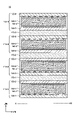
- FIG. 2A and 2B are schematic cross-sectional views of the optical element 10 according to one embodiment of the present invention.
- FIG. 2A is a schematic cross-sectional view in the zx plane cut along the A1-A2 line shown in FIG. 1
- FIG. 2B is a schematic cross-sectional view along the B1-B2 line shown in FIG. It is a schematic cross-sectional view in the cut yz-plane.
- the x-axis direction and the y-axis direction may be described as the first direction and the second direction, respectively.
- the first liquid crystal cell 110-1 includes a first substrate 120-1 on which a first transparent electrode 130-1 and a second transparent electrode 130-2 are formed, a third transparent electrode 130-3 and a third transparent electrode 130-3. and a second substrate 120-2 on which four transparent electrodes 130-4 are formed.
- a first alignment film 140-1 is formed on the first substrate 120-1 to cover the first transparent electrode 130-1 and the second transparent electrode 130-2.
- a second alignment film 140-2 is formed on the second substrate 120-2 to cover the third transparent electrode 130-3 and the fourth transparent electrode 130-4.
- the first substrate 120-1 and the second substrate 120-2 are composed of the first transparent electrode 130-1 and the second transparent electrode 130-2 on the first substrate 120-1 and the second substrate.
- a third transparent electrode 130-3 and a fourth transparent electrode 130-4 on 120-2 are arranged to face each other.
- a first sealing member 150-1 is formed on the periphery of each of the first substrate 120-1 and the second substrate 120-2. That is, the first substrate 120-1 and the second substrate 120-2 are adhered via the first sealing material 150-1. Also, the first substrate 120-1 (more specifically, the first alignment film 140-1), the second substrate 120-2 (more specifically, the second alignment film 140-2), And the space surrounded by the first sealing material 150-1 is filled with liquid crystal to form a first liquid crystal layer 160-1.
- the second liquid crystal cell 110-2 includes a third substrate 120-3 on which a fifth transparent electrode 130-5 and a sixth transparent electrode 130-6 are formed, a seventh transparent electrode 130-7 and a third substrate 130-7. and a fourth substrate 120-4 on which eight transparent electrodes 130-8 are formed.
- a third alignment film 140-3 is formed on the third substrate 120-3 to cover the fifth transparent electrode 130-5 and the sixth transparent electrode 130-6.
- a fourth alignment film 140-4 covering the seventh transparent electrode 130-7 and the eighth transparent electrode 130-8 is formed on the fourth substrate 120-4.
- the third substrate 120-3 and the fourth substrate 120-4 are composed of the fifth transparent electrode 130-5 and the sixth transparent electrode 130-6 on the third substrate 120-3 and the fourth substrate.
- a seventh transparent electrode 130-7 and an eighth transparent electrode 130-8 on 120-4 are arranged to face each other.
- a second sealing material 150-2 is formed on the periphery of each of the third substrate 120-3 and the fourth substrate 120-4. That is, the third substrate 120-3 and the fourth substrate 120-4 are adhered via the second sealing material 150-2. Further, a third substrate 120-3 (more specifically, a third alignment film 140-3), a fourth substrate 120-4 (more specifically, a fourth alignment film 140-4), And the space surrounded by the second sealing material 150-2 is filled with liquid crystal to form a second liquid crystal layer 160-2.
- the third liquid crystal cell 110-3 includes a fifth substrate 120-5 on which a ninth transparent electrode 130-9 and a tenth transparent electrode 130-10 are formed, an eleventh transparent electrode 130-11 and a third substrate 120-5. and a sixth substrate 120-6 on which twelve transparent electrodes 130-12 are formed.
- a fifth alignment film 140-5 covering the ninth transparent electrode 130-9 and the tenth transparent electrode 130-10 is formed on the fifth substrate 120-5.
- a sixth alignment film 140-6 covering the eleventh transparent electrode 130-11 and the twelfth transparent electrode 130-12 is formed on the sixth substrate 120-6.
- the fifth substrate 120-5 and the sixth substrate 120-6 are composed of the ninth transparent electrode 130-9 and the tenth transparent electrode 130-10 on the fifth substrate 120-5 and the sixth substrate.
- the eleventh transparent electrode 130-11 and the twelfth transparent electrode 130-12 on 120-6 are arranged to face each other.
- a third sealing material 150-3 is formed around the periphery of each of the fifth substrate 120-5 and the sixth substrate 120-6. That is, the fifth substrate 120-5 and the sixth substrate 120-6 are adhered via the third sealing material 150-3.
- a fifth substrate 120-5 (more specifically, a fifth alignment film 140-5), a sixth substrate 120-6 (more specifically, a sixth alignment film 140-6), And a space surrounded by the third sealing material 150-3 is filled with liquid crystal to form a third liquid crystal layer 160-3.
- the fourth liquid crystal cell 110-4 includes a seventh substrate 120-7 on which a 13th transparent electrode 130-13 and a 14th transparent electrode 130-14 are formed, a 15th transparent electrode 130-15 and a 15th transparent electrode 130-15. and an eighth substrate 120-8 on which 16 transparent electrodes 130-16 are formed.
- a seventh alignment film 140-7 covering the thirteenth transparent electrode 130-13 and the fourteenth transparent electrode 130-14 is formed on the seventh substrate 120-7.
- An eighth alignment film 140-8 is formed on the eighth substrate 120-8 to cover the fifteenth transparent electrode 130-15 and the sixteenth transparent electrode 130-16.
- the seventh substrate 120-7 and the eighth substrate 120-8 are composed of the thirteenth transparent electrode 130-13 and the fourteenth transparent electrode 130-14 on the seventh substrate 120-7 and the eighth substrate.
- a fifteenth transparent electrode 130-15 and a sixteenth transparent electrode 130-16 on 120-8 are arranged to face each other.
- a fourth sealing material 150-4 is formed around the periphery of each of the seventh substrate 120-7 and the eighth substrate 120-8. That is, the seventh substrate 120-7 and the eighth substrate 120-8 are adhered via the fourth sealing material 150-4.
- the seventh substrate 120-7 (more specifically, the seventh alignment film 140-7), the eighth substrate 120-8 (more specifically, the eighth alignment film 140-8), And the space surrounded by the fourth sealing material 150-4 is filled with liquid crystal to form a fourth liquid crystal layer 160-4.
- the basic configurations of the first liquid crystal cell 110-1, the second liquid crystal cell 110-2, the third liquid crystal cell 110-3, and the fourth liquid crystal cell 110-4 are the same. However, the arrangement of the transparent electrode 130 is different.
- the first transparent electrode 130-1 and the second transparent electrode 130-2 extend in the y-axis direction
- the third transparent electrode 130-3 and the fourth transparent electrode 130-4 extends in the x-axis direction
- the first transparent electrode 130-1 and the second transparent electrode 130-2 are alternately arranged in a comb shape in the x-axis direction
- the third transparent electrode 130-3 and the fourth transparent electrode 130 are arranged alternately
- -4 are alternately arranged in a comb shape in the y-axis direction.
- the extending direction (y-axis direction) of the first transparent electrode 130-1 and the second transparent electrode 130-2 is the same as that of the third transparent electrode 130-3 and the fourth transparent electrode 130-4. Although it is orthogonal to the extending direction (x-axis direction), it may intersect with a slight deviation.
- the fifth transparent electrode 130-5 and the sixth transparent electrode 130-6 extend in the y-axis direction
- the seventh transparent electrode 130-7 and the eighth transparent electrode 130-8 extends in the x-axis direction.
- the fifth transparent electrode 130-5 and the sixth transparent electrode 130-6 are alternately arranged in a comb shape in the x-axis direction
- the seventh transparent electrode 130-7 and the eighth transparent electrode 130 are arranged alternately.
- -8 are alternately arranged in a comb shape in the y-axis direction.
- the extending direction (y-axis direction) of the fifth transparent electrode 130-5 and the sixth transparent electrode 130-6 is the same as that of the seventh transparent electrode 130-7 and the eighth transparent electrode 130-8. Although it is orthogonal to the extending direction (x-axis direction), it may intersect with a slight deviation.
- the ninth transparent electrode 130-9 and the tenth transparent electrode 130-10 extend in the x-axis direction, and the eleventh transparent electrode 130-11 and the twelfth transparent electrode 130-12 extends in the y-axis direction. Further, the ninth transparent electrode 130-9 and the tenth transparent electrode 130-10 are alternately arranged in the y-axis direction in a comb shape, and the eleventh transparent electrode 130-11 and the twelfth transparent electrode 130 are arranged alternately. ⁇ 12 are alternately arranged in a comb shape in the x-axis direction.
- the extending direction (x-axis direction) of the ninth transparent electrode 130-9 and the tenth transparent electrode 130-10 is the same as that of the eleventh transparent electrode 130-11 and the twelfth transparent electrode 130-12. Although it is orthogonal to the extending direction (y-axis direction), it may intersect with a slight deviation.
- the 13th transparent electrode 130-13 and the 14th transparent electrode 130-14 extend in the x-axis direction, and the 15th transparent electrode 130-15 and the 16th transparent electrode 130-15 extend in the x-axis direction.
- 130-16 extends in the y-axis direction.
- the 13th transparent electrode 130-13 and the 14th transparent electrode 130-14 are alternately arranged in a comb shape in the y-axis direction, and the 15th transparent electrode 130-15 and the 16th transparent electrode 130-130 are arranged alternately.
- -16 are alternately arranged in a comb shape in the x-axis direction.
- the extending direction (x-axis direction) of the 13th transparent electrode 130-13 and the 14th transparent electrode 130-14 is the same as that of the 15th transparent electrode 130-15 and the 16th transparent electrode 130-16. Although it is orthogonal to the extending direction (y-axis direction), it may intersect with a slight deviation.
- the 11th transparent electrode 130-11 and the 15th transparent electrode 130-15 of the fourth liquid crystal cell 110-4 are superimposed so that their extending directions (y-axis direction) substantially coincide with each other.
- the first transparent electrode 130-1, the fifth transparent electrode 130-5, the eleventh transparent electrode 130-11, and the fifteenth transparent electrode 130-15 overlap each other with a slight shift.
- liquid crystal cell 110-1 to fourth liquid crystal cell 110-4 may be arranged.
- each of the first substrate 120-1 to the eighth substrate 120-8 for example, a transparent rigid substrate such as a glass substrate, a quartz substrate, or a sapphire substrate is used. Further, as each of the first substrate 120-1 to the eighth substrate 120-8, for example, a flexible substrate having translucency such as a polyimide resin substrate, an acrylic resin substrate, a siloxane resin substrate, or a fluorine resin substrate. can also be used.
- Each of the first transparent electrode 130 - 1 to the sixteenth transparent electrode 130 - 16 functions as an electrode for forming an electric field in the liquid crystal layer 160 .
- a transparent conductive material such as indium tin oxide (ITO) or indium zinc oxide (IZO) is used for each of the first transparent electrode 130-1 to the sixteenth transparent electrode 130-16.
- Each of the first liquid crystal layer 160-1 to the fourth liquid crystal layer 160-4 can refract transmitted light or change the polarization state of transmitted light according to the alignment state of the liquid crystal molecules.
- Nematic liquid crystal or the like is used as the liquid crystal for each of the first liquid crystal layer 160-1 to the fourth liquid crystal layer 160-4.
- the liquid crystal described in this embodiment is of a positive type, it is also possible to apply a negative type by changing the initial alignment direction of the liquid crystal molecules. Further, the liquid crystal preferably contains a chiral agent that imparts twist to the liquid crystal molecules.
- Each of the first alignment film 140-1 to the eighth alignment film 140-8 aligns liquid crystal molecules in the liquid crystal layer 160 in a predetermined direction.
- a polyimide resin or the like is used for each of the first to eighth alignment films 140-1 to 140-8.
- Each of the first alignment film 140-1 to the eighth alignment film 140-8 may be imparted with alignment properties by an alignment treatment such as a rubbing method or a photo-alignment method.
- the rubbing method is a method of rubbing the surface of the alignment film in one direction.
- the photo-alignment method is a method of irradiating an alignment film with linearly polarized ultraviolet rays.
- An adhesive containing epoxy resin or acrylic resin is used as each of the first sealing material 150-1 to the fourth sealing material 150-4.
- the adhesive may be of an ultraviolet curing type or a thermosetting type.
- the optical element 10 includes at least two liquid crystal cells (eg, a first liquid crystal cell 110-1 and a second liquid crystal cell 110-2) to control the light distribution of unpolarized light. Therefore, on each surface of the first substrate 120-1 of the first liquid crystal cell 110-1 and the eighth substrate 120-8 of the fourth liquid crystal cell 110-4, for example, on the front and back surfaces of the liquid crystal display element. There is no need to provide a pair of polarizers as provided.
- 3A and 3B are schematic cross-sectional views illustrating control of light distribution by the optical element 10 according to one embodiment of the present invention.
- 3A and 3B show part of the cross-sectional view of the first liquid crystal cell 110-1 and the second liquid crystal cell 110-2 shown in FIG. 2A.
- 3A shows the optical element 10 with no potential applied to the transparent electrode 130
- FIG. 3B shows the optical element 10 with a potential applied to the transparent electrode 130.
- the first alignment film 140-1 is oriented in the x-axis direction. Therefore, as shown in FIG. 3A, the long axis of the liquid crystal molecules on the first substrate 120-1 side of the first liquid crystal layer 160-1 is oriented along the x-axis direction. That is, the alignment direction of the liquid crystal molecules on the first substrate 120-1 side is orthogonal to the extending direction (y-axis direction) of the first transparent electrode 130-1 and the second transparent electrode 130-2. there is Also, the second alignment film 140-2 is oriented in the y-axis direction. Therefore, as shown in FIG. 3A, the long axis of the liquid crystal molecules on the second substrate 120-2 side of the first liquid crystal layer 160-1 is aligned along the y-axis direction.
- the alignment direction of the liquid crystal molecules on the second substrate 120-2 side is perpendicular to the extending direction (x-axis direction) of the third transparent electrode 130-3 and the fourth transparent electrode 130-4.
- the liquid crystal molecules of the first liquid crystal layer 160-1 gradually change the direction of the long axis from the x-axis direction to the y-axis direction from the first substrate 120-1 to the second substrate 120-2. , is oriented with a 90° twist.
- the liquid crystal molecules of the second liquid crystal layer 160-2 are also the same as the liquid crystal molecules of the first liquid crystal layer 160-1, so the explanation is omitted here.
- the orientation of the liquid crystal molecules changes as shown in FIG. 3B.
- a low potential is supplied to the first transparent electrode 130-1, the third transparent electrode 130-3, the fifth transparent electrode 130-5, and the seventh transparent electrode 130-7, and the second transparent electrode 130-7 is supplied with a low potential.
- the electrode 130-2, the fourth transparent electrode 130-4, the sixth transparent electrode 130-6, and the eighth transparent electrode 130-8 are supplied with a high potential.
- the low potential and the high potential are illustrated using the symbols "-" and "+", respectively.
- the electric field which arises between the transparent electrodes which adjoin may be called a horizontal electric field.
- the liquid crystal molecules on the side of the first substrate 120-1 as a whole are It is oriented in a convex arc along the x-axis direction with respect to the first substrate 120-1.
- the liquid crystal molecules on the side of the second substrate 120-2 as a whole move toward the second substrate. 120-2 along the y-axis direction in a convex arc.
- Liquid crystal molecules positioned substantially in the center between the first transparent electrode 130-1 and the second transparent electrode 130-2 have almost no orientation change due to any lateral electric field.
- the light incident on the first liquid crystal layer 160-1 moves in the x-axis direction according to the refractive index distribution of the liquid crystal molecules aligned in a convex circular shape along the x-axis direction on the first substrate 120-1 side.
- the light is diffused in the y-axis direction according to the refractive index distribution of the liquid crystal molecules aligned in a convex arc along the y-axis direction on the second substrate 120-2 side.
- the first transparent electrode 130-1 of the first substrate 120-1 and the second transparent electrode 130-2 does not affect the orientation of the liquid crystal molecules on the second substrate 120-2 side, or is so small that it can be ignored.
- the lateral electric field between the third transparent electrode 130-3 and the fourth transparent electrode 130-4 on the second substrate 120-2 is applied to the orientation of the liquid crystal molecules on the first substrate 120-1 side. have no effect or are so small as to be negligible.
- the liquid crystal molecules of the second liquid crystal layer 160-2 when a potential is supplied to the fifth transparent electrode 130-5 to the eighth transparent electrode 130-8 are also the liquid crystal molecules of the first liquid crystal layer 160-1. Since it is the same, the explanation is omitted here.
- Light emitted from a light source has a polarized component in the x-axis direction (P-polarized component) and a polarized component in the y-axis direction (S-polarized component). It will be described separately from the polarization component. That is, the light emitted from the light source (see (1) in FIGS. 3A and 3B) includes a first polarized light 310 having a P-polarized component and a second polarized light 320 having an S-polarized component. 3A and 3B, the arrow symbol and the circle symbol with a cross represent the P-polarized component and the S-polarized component, respectively.
- the first polarized light 310 After being incident on the first substrate 120-1, the first polarized light 310 changes from the P-polarized component to the S-polarized component according to the twist of the orientation of the liquid crystal molecules as it moves toward the second substrate 120-2 (Fig. 3A and (2)-(4) in FIG. 3B). More specifically, the first polarized light 310 has a polarization axis in the x-axis direction on the first substrate 120-1 side, but passes through the thickness direction of the first liquid crystal layer 160-1. The polarization axis is gradually changed in the process, and the second substrate 120-2 side has the polarization axis in the y-axis direction, and then is emitted from the second substrate 120-2 side (FIGS. 3A and 3B). See (5) inside).
- the liquid crystal molecules on the first substrate 120-1 side move to the x-axis due to the influence of the horizontal electric field. It is oriented in a convex circular shape along the direction, and the refractive index distribution changes. Therefore, the first polarized light 310 diffuses in the x-axis direction according to the refractive index distribution of the liquid crystal molecules. Further, when a horizontal electric field is generated between the third transparent electrode 130-3 and the fourth transparent electrode 130-4, the liquid crystal molecules on the second substrate 120-2 side move in the y-axis direction due to the influence of the horizontal electric field. , and the refractive index distribution changes. Therefore, the first polarized light 310 diffuses in the y-axis direction according to changes in the refractive index distribution of the liquid crystal molecules.
- the polarization component of the first polarized light 310 transmitted through the first liquid crystal cell 110-1 changes from the P polarized component to the S polarized component.
- the first polarized light 310 transmitted through the first liquid crystal cell changes its polarization component from the P-polarized component to the S-polarized component, Diffuse in the y-axis direction.
- the second polarized light 320 After being incident on the first substrate 120-1, the second polarized light 320 changes from the S-polarized component to the P-polarized component according to the twist of the orientation of the liquid crystal molecules as it moves toward the second substrate 120-2 (Fig. 3A and (2)-(4) in FIG. 3B). More specifically, the second polarized light 320 has a polarization axis in the y-axis direction on the first substrate 120-1 side, but passes through the thickness direction of the first liquid crystal layer 160-1. The polarization axis is gradually changed in the process, and the second substrate 120-2 side has the polarization axis in the x-axis direction, and then is emitted from the second substrate 120-2 side (FIGS. 3A and 3B). See (5) inside).
- the liquid crystal molecules on the first substrate 120-1 side move to the x-axis due to the influence of the horizontal electric field. It is oriented in a convex circular shape along the direction, and the refractive index distribution changes.
- the polarization axis of the second polarized light 320 is orthogonal to the alignment of the liquid crystal molecules on the first substrate 120-1 side, it is not affected by the refractive index distribution of the liquid crystal molecules and is not diffused. pass.
- the liquid crystal molecules on the second substrate 120-2 side move in the y-axis direction due to the influence of the horizontal electric field. , and the refractive index distribution changes.
- the polarization axis of the second polarized light 320 is orthogonal to the orientation of the liquid crystal molecules on the second substrate 120-2 side, it is not affected by the refractive index distribution of the liquid crystal molecules and is not diffused. pass.
- the second polarized light 320 transmitted through the first liquid crystal cell 110-1 not only when no lateral electric field is generated (see FIG. 3A) but also when a lateral electric field is generated (see FIG. 3B) changes the polarization component from the S polarization component to the P polarization component, but does not diffuse.
- the liquid crystal molecules of the second liquid crystal layer 160-2 of the second liquid crystal cell 110-2 also have the same refractive index distribution as the liquid crystal molecules of the first liquid crystal layer 160-1 of the first liquid crystal cell 110-1. .
- the liquid crystal molecules of the second liquid crystal layer 160-2 The polarization affected by the refractive index profile is reversed. That is, not only when no lateral electric field is generated (see FIG. 3A), but also when a lateral electric field is generated (see FIG.
- the first polarized light 310 transmitted through the second liquid crystal cell 110-2 changes the polarization component from the S polarization component to the P polarization component, but does not diffuse (see (6) to (8) in FIGS. 3A and 3B).
- the polarization component of the second polarized light 320 transmitted through the second liquid crystal cell 110-2 only changes from the P polarized component to the S polarized component.
- the second polarized light 320 transmitted through the second liquid crystal cell 110-2 changes from the P polarized component to the S polarized component, and the x Diffuse in the axial direction and the y-axis direction.
- the optical element 10 by stacking two liquid crystal cells 110 having the same structure, the polarization component of the light incident on the optical element 10 is changed twice.
- the polarization components after incidence can be left unchanged (see (1) and (9) in FIGS. 3A and 3B).
- the optical element 10 can apply a potential to the transparent electrode 130 to change the refractive index distribution of the liquid crystal molecules of the liquid crystal layer 160 of the liquid crystal cell 110 and refract light passing through the liquid crystal cell 110 .
- the first liquid crystal cell 110-1 diffuses the light of the first polarized light 310 (P-polarized component) in the x-axis direction, the y-axis direction, or both the x-axis and y-axis directions
- the second liquid crystal cell 110-2 can diffuse the light of the second polarized light 320 (S-polarized component) in the x-axis direction, the y-axis direction, or both the x-axis and y-axis directions.
- FIGS. 3A and 3B show only the first liquid crystal cell 110-1 and the second liquid crystal cell 110-2, and the light transmitted through the first liquid crystal cell 110-1 and the second liquid crystal cell 110-2
- the light distribution has been described, the light distribution of light passing through the third liquid crystal cell 110-3 and the fourth liquid crystal cell 110-4 is the same.
- the third liquid crystal cell 110-3 and the fourth liquid crystal cell 110-4 are laminated while being rotated 90 degrees with respect to the first liquid crystal cell 110-1 and the second liquid crystal cell 110-2.
- the acting polarization components are interchanged.
- the third liquid crystal cell 110-3 diffuses the light of the second polarized light 320 (S-polarized component) in the x-axis direction, the y-axis direction, or both the x-axis and y-axis directions.
- Cell 110-4 can scatter light of the first polarization 310 (the P polarization component) along the x-axis, the y-axis, or both the x- and y-axes.
- FIG. 4 is a schematic diagram illustrating connection of the transparent electrodes 130 of the optical element 10 according to one embodiment of the present invention.
- the first transparent electrode 130-1 and the fifteenth transparent electrode 130-15 are connected to a first potential supply line 200-1 that supplies a first potential V1. That is, the first transparent electrode 130-1 and the fifteenth transparent electrode 130-15 are electrically connected to each other.
- the second transparent electrode 130-2 and the sixteenth transparent electrode 130-16 are connected to a second potential supply line 200-2 that supplies the second potential V2. That is, the second transparent electrode 130-2 and the sixteenth transparent electrode 130-16 are electrically connected to each other.
- the third transparent electrode 130-3 and the thirteenth transparent electrode 130-13 are connected to a third potential supply line 200-3 that supplies the third potential V3. That is, the third transparent electrode 130-3 and the thirteenth transparent electrode 130-13 are electrically connected to each other.
- the fourth transparent electrode 130-4 and the fourteenth transparent electrode 130-14 are connected to a fourth potential supply line 200-4 that supplies the fourth potential V4. That is, the fourth transparent electrode 130-4 and the fourteenth transparent electrode 130-14 are electrically connected to each other.
- the fifth transparent electrode 130-5 and the eleventh transparent electrode 130-11 are connected to a fifth potential supply line 200-5 that supplies a fifth potential V5. That is, the fifth transparent electrode 130-5 and the eleventh transparent electrode 130-11 are electrically connected to each other.
- the sixth transparent electrode 130-6 and the twelfth transparent electrode 130-12 are connected to a sixth potential supply line 200-6 that supplies a sixth potential V6. That is, the sixth transparent electrode 130-6 and the twelfth transparent electrode 130-12 are electrically connected to each other.
- the seventh transparent electrode 130-7 and the ninth transparent electrode 130-9 are connected to a seventh potential supply line 200-7 that supplies a seventh potential V7. That is, the seventh transparent electrode 130-7 and the ninth transparent electrode 130-9 are electrically connected to each other.
- the eighth transparent electrode 130-8 and the tenth transparent electrode 130-10 are connected to an eighth potential supply line 200-8 that supplies an eighth potential V8. That is, the eighth transparent electrode 130-8 and the tenth transparent electrode 130-10 are electrically connected to each other.
- the first potential V1 to the eighth potential V8 may be fixed potentials or variable potentials. Not only the low potential and the high potential but also an intermediate potential between the low potential and the high potential are supplied to the first potential supply line 200-1 to the eighth potential supply line 200-8. That is, the first potential V1 to the eighth potential include three potentials with different absolute values. Thereby, the optical element 10 can diffuse the light emitted from the light source in an elliptical shape in which the minor axis and the major axis are adjusted. An elliptical example will be described below.
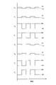
- FIG. 5A is a timing chart showing potentials supplied to the transparent electrode 130 of the optical element 10 according to one embodiment of the present invention.
- the first potential V1 and the second potential V2 are variable potentials obtained by inverting the intermediate potential. That is, the first potential V1 and the second potential V2 are potentials in which ⁇ 2V and +2V are repeated. However, the phases of the first potential V1 and the second potential V2 are reversed. Therefore, the absolute value of the potential difference between the first potential V1 and the second potential V2 is 4V.
- the third potential V3 and the fourth potential V4 are variable potentials in which the low potential and the high potential are reversely driven. That is, the third potential V3 and the fourth potential V4 are potentials in which ⁇ 5V and +5V are repeated. However, the phases of the third potential V3 and the fourth potential V4 are reversed. Therefore, the absolute value of the potential difference between the third potential V3 and the fourth potential V4 is 10V.
- the fifth potential V5 and the sixth potential V6 are intermediate fixed potentials. That is, the fifth potential V5 and the sixth potential V6 are 0V.
- the seventh potential V7 and the eighth potential V8 are variable potentials in which the low potential and the high potential are reversely driven. That is, the seventh potential V7 and the eighth potential V8 are potentials in which ⁇ 5V and +5V are repeated. However, the phases of the seventh potential V7 and the eighth potential V8 are reversed. Therefore, the absolute value of the potential difference between the seventh potential V7 and the eighth potential V8 is 10V.
- the alignment state of the liquid crystal molecules of the liquid crystal layer 160 changes according to the potential difference.
- Light polarized in the x-axis direction (for example, a P-polarized component) incident on the optical element 10 is generated by the potential difference (4 V) between the first transparent electrode 130-1 and the second transparent electrode 130-2 and the 15th It is diffused in the x-axis direction by the potential difference (4 V) between the transparent electrode 130-15 and the sixteenth transparent electrode 130-16.
- the light polarized in the x-axis direction incident on the optical element 10 is generated by the potential difference (10 V) between the third transparent electrode 130-3 and the fourth transparent electrode 130-4 and the potential difference (10 V) between the third transparent electrode 130-3 and the fourth transparent electrode 130-4. and the fourteenth transparent electrode 130-14.
- the light polarized in the y-axis direction (for example, the S-polarized component) incident on the optical element 10 has the potential difference (10 V) between the seventh transparent electrode 130-7 and the eighth transparent electrode 130-8 and the The light is diffused in the y-axis direction by the potential difference (10 V) between the 9th transparent electrode 130-9 and the 10th transparent electrode 130-10.
- the light transmitted through the optical element 10 has an elliptical light distribution having a minor axis in the x-axis direction and a major axis in the y-axis direction.
- the light polarized in the x-axis direction is diffused in the x-axis direction in the timing chart shown in FIG. 5A, it is also possible to diffuse the light polarized in the y-axis direction in the x-axis direction. This will be explained below.
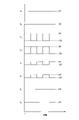
- FIG. 5B is a timing chart showing potentials supplied to the transparent electrode 130 of the optical element 10 according to one embodiment of the present invention.
- the first potential V1 and the second potential V2 are intermediate fixed potentials. That is, the first potential V1 and the second potential V2 are 0V.
- the third potential V3 and the fourth potential V4 are variable potentials in which the low potential and the high potential are reversely driven. That is, the third potential V3 and the fourth potential V4 are potentials in which ⁇ 5V and +5V are repeated. However, the phases of the third potential V3 and the fourth potential V4 are reversed. Therefore, the absolute value of the potential difference between the third potential V3 and the fourth potential V4 is 10V.
- the fifth potential V5 and the sixth potential V6 are variable potentials obtained by inverting the intermediate potential. That is, the fifth potential V5 and the sixth potential V6 are potentials in which ⁇ 2V and +2V are repeated. However, the phases of the fifth potential V5 and the sixth potential V6 are reversed. Therefore, the absolute value of the potential difference between the fifth potential V5 and the sixth potential V6 is 4V.
- the seventh potential V7 and the eighth potential V8 are variable potentials in which the low potential and the high potential are reversely driven. That is, the seventh potential V7 and the eighth potential V8 are potentials in which ⁇ 5V and +5V are repeated. However, the phases of the seventh potential V7 and the eighth potential V8 are reversed. Therefore, the absolute value of the potential difference between the seventh potential V7 and the eighth potential V8 is 10V.
- the alignment state of the liquid crystal molecules of the liquid crystal layer 160 changes according to the potential difference.
- the light polarized in the y-axis direction incident on the optical element 10 is generated by the potential difference (4 V) between the fifth transparent electrode 130-5 and the sixth transparent electrode 130-6 and the potential difference (4 V) between the eleventh transparent electrode 130-11 and the 11th transparent electrode 130-11. It is diffused in the x-axis direction by the potential difference (4 V) with the twelve transparent electrodes 130-12.
- the light polarized in the y-axis direction incident on the optical element 10 is generated by the potential difference (10 V) between the seventh transparent electrode 130-7 and the eighth transparent electrode 130-8 and the ninth transparent electrode 130-9.
- the light polarized in the x-axis direction incident on the optical element 10 is generated by the potential difference (10 V) between the third transparent electrode 130-3 and the fourth transparent electrode 130-4 and the potential difference (10 V) between the third transparent electrode 130-3 and the fourth transparent electrode 130-4. and the fourteenth transparent electrode 130-14. Therefore, of the light incident on the optical element 10, part of the light polarized in the y-axis direction is diffused in the x-axis direction, and the rest of the light is diffused in the y-axis direction. Therefore, the light transmitted through the optical element 10 has an elliptical light distribution having a minor axis in the x-axis direction and a major axis in the y-axis direction.
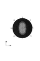
- FIG. 5C is a measurement result of measuring the azimuth angle of light transmitted through the optical element 10 according to one embodiment of the present invention.
- the potential shown in the timing chart shown in FIG. 5A was supplied to the manufactured optical element 10, an elliptical light distribution shown in FIG. 5C was measured.
- FIG. 6A is a timing chart showing potentials supplied to the transparent electrode 130 of the optical element 10 according to one embodiment of the present invention.
- the first potential V1 and the second potential V2 are variable potentials obtained by inverting the intermediate potential. That is, the first potential V1 and the second potential V2 are potentials in which ⁇ 1V and +1V are repeated. However, the phases of the first potential V1 and the second potential V2 are reversed. Therefore, the absolute value of the potential difference between the first potential V1 and the second potential V2 is 2V.
- the third potential V3 and the fourth potential V4 are variable potentials in which the low potential and the high potential are reversely driven. That is, the third potential V3 and the fourth potential V4 are potentials in which ⁇ 5V and +5V are repeated. However, the phases of the third potential V3 and the fourth potential V4 are reversed. Therefore, the absolute value of the potential difference between the third potential V3 and the fourth potential V4 is 10V.
- the fifth potential V5 and the sixth potential V6 are variable potentials obtained by inverting the intermediate potential. That is, the fifth potential V5 and the sixth potential V6 are potentials in which ⁇ 1V and +1V are repeated. However, the phases of the fifth potential V5 and the sixth potential V6 are reversed. Therefore, the absolute value of the potential difference between the fifth potential V5 and the sixth potential V6 is 2V.
- the seventh potential V7 and the eighth potential V8 are variable potentials in which the low potential and the high potential are reversely driven. That is, the seventh potential V7 and the eighth potential V8 are potentials in which ⁇ 5V and +5V are repeated. However, the phases of the seventh potential V7 and the eighth potential V8 are reversed. Therefore, the absolute value of the potential difference between the seventh potential V7 and the eighth potential V8 is 10V.
- the alignment state of the liquid crystal molecules of the liquid crystal layer 160 changes according to the potential difference.
- Light polarized in the x-axis direction (for example, a P-polarized component) incident on the optical element 10 is generated by the potential difference (2 V) between the first transparent electrode 130-1 and the second transparent electrode 130-2 and the 15th Due to the potential difference (2 V) between the transparent electrode 130-15 and the sixteenth transparent electrode 130-16, the light is slightly diffused in the x-axis direction.
- the light polarized in the x-axis direction incident on the optical element 10 is generated by the potential difference (10 V) between the third transparent electrode 130-3 and the fourth transparent electrode 130-4 and the potential difference (10 V) between the third transparent electrode 130-3 and the fourth transparent electrode 130-4. and the fourteenth transparent electrode 130-14.
- the light polarized in the y-axis direction (for example, the S-polarized component) incident on the optical element 10 has the potential difference (2 V) between the fifth transparent electrode 130-5 and the sixth transparent electrode 130-6 and the The potential difference (2 V) between the 11th transparent electrode 130-11 and the 12th transparent electrode 130-12 slightly diffuses in the x-axis direction.
- the light transmitted through the optical element 10 has an elliptical light distribution that is close to a circle having a minor axis in the x-axis direction and a major axis in the y-axis direction.
- FIG. 6B is a measurement result of measuring the azimuth angle of light transmitted through the optical element 10 according to one embodiment of the present invention.
- an elliptical light distribution shown in FIG. 6B was measured.
- the degree of diffusion in the x-axis direction is higher than in the first specific example. More specifically, not only a portion of the light polarized in the x-axis direction but also a portion of the light polarized in the y-axis direction is diffused in the x-axis direction. Therefore, the light distribution state of the present specific example 2 shown in FIG. 6B became an elliptical light distribution closer to a circle than the light distribution state of the specific example 1 shown in FIG. 5C.
- FIG. 7A is a timing chart showing potentials supplied to the transparent electrode 130 of the optical element 10 according to one embodiment of the present invention.
- the first potential V1 and the second potential V2 are variable potentials in which the low potential and the high potential are reversely driven. That is, the first potential V1 and the second potential V2 are potentials in which ⁇ 5V and +5V are repeated. However, the phases of the first potential V1 and the second potential V2 are reversed. Therefore, the absolute value of the potential difference between the first potential V1 and the second potential V2 is 10V.
- the third potential V3 and the fourth potential V4 are variable potentials obtained by inverting the intermediate potential. That is, the third potential V3 and the fourth potential V4 are potentials in which ⁇ 2V and +2V are repeated. However, the phases of the third potential V3 and the fourth potential V4 are reversed. Therefore, the absolute value of the potential difference between the third potential V3 and the fourth potential V4 is 4V.
- the fifth potential V5 and the sixth potential V6 are variable potentials in which the low potential and the high potential are reversely driven. That is, the fifth potential V5 and the sixth potential V6 are potentials in which ⁇ 5V and +5V are repeated. However, the phases of the fifth potential V5 and the sixth potential V6 are reversed. Therefore, the absolute value of the potential difference between the fifth potential V5 and the sixth potential V6 is 10V.
- the seventh potential V7 and the eighth potential V8 are intermediate fixed potentials. That is, the seventh potential V7 and the eighth potential V8 are 0V.
- the alignment state of the liquid crystal molecules of the liquid crystal layer 160 changes according to the potential difference.
- Light polarized in the x-axis direction (for example, a P-polarized component) incident on the optical element 10 is generated by the potential difference (4 V) between the third transparent electrode 130-3 and the fourth transparent electrode 130-4 and the potential difference (4 V) between the third transparent electrode 130-3 and the fourth transparent electrode .
- the light is diffused in the y-axis direction by the potential difference (4 V) between the transparent electrode 130-13 and the fourteenth transparent electrode 130-14.
- the light polarized in the x-axis direction incident on the optical element 10 is generated by the potential difference (10 V) between the first transparent electrode 130-1 and the second transparent electrode 130-2 and the potential difference (10 V) between the fifteenth transparent electrode 130-15. and the sixteenth transparent electrode 130-16.
- the light polarized in the y-axis direction (for example, the S-polarized component) incident on the optical element 10 has the potential difference (10 V) between the fifth transparent electrode 130-5 and the sixth transparent electrode 130-6 and the The potential difference (10 V) between the 11th transparent electrode 130-11 and the 12th transparent electrode 130-12 diffuses in the x-axis direction.
- the light transmitted through the optical element 10 has an elliptical light distribution having a major axis in the x-axis direction and a minor axis in the y-axis direction.
- the light polarized in the x-axis direction is diffused in the y-axis direction in the timing chart shown in FIG. 7A, it is also possible to diffuse the light polarized in the y-axis direction in the y-axis direction. This will be explained below.
- FIG. 7B is a timing chart showing potentials supplied to the transparent electrode 130 of the optical element 10 according to one embodiment of the present invention.
- the first potential V1 and the second potential V2 are variable potentials in which the low potential and the high potential are reversely driven. That is, the first potential V1 and the second potential V2 are potentials in which ⁇ 5V and +5V are repeated. However, the phases of the first potential V1 and the second potential V2 are reversed. Therefore, the absolute value of the potential difference between the first potential V1 and the second potential V2 is 10V.
- the third potential V3 and the fourth potential V4 are intermediate fixed potentials. That is, the third potential V3 and the fourth potential V4 are 0V.
- the fifth potential V5 and the sixth potential V6 are variable potentials in which the low potential and the high potential are reversely driven. That is, the fifth potential V5 and the sixth potential V6 are potentials in which ⁇ 5V and +5V are repeated. However, the phases of the fifth potential V5 and the sixth potential V6 are reversed. Therefore, the absolute value of the potential difference between the fifth potential V5 and the sixth potential V6 is 10V.
- the seventh potential V7 and the eighth potential V8 are variable potentials obtained by inverting the intermediate potential. That is, the seventh potential V7 and the eighth potential V8 are potentials in which ⁇ 2V and +2V are repeated. However, the phases of the seventh potential V7 and the eighth potential V8 are reversed. Therefore, the absolute value of the potential difference between the seventh potential V7 and the eighth potential V8 is 4V.
- the alignment state of the liquid crystal molecules of the liquid crystal layer 160 changes according to the potential difference.
- the light polarized in the y-axis direction incident on the optical element 10 is generated by the potential difference (4 V) between the seventh transparent electrode 130-7 and the eighth transparent electrode 130-8 and the potential difference (4 V) between the ninth transparent electrode 130-9 and the ninth transparent electrode 130-9. It is diffused in the y-axis direction by the potential difference (4 V) with the ten transparent electrodes 130-10. Further, the light polarized in the y-axis direction incident on the optical element 10 is generated by the potential difference (10 V) between the fifth transparent electrode 130-5 and the sixth transparent electrode 130-6 and the eleventh transparent electrode 130-11.
- the light polarized in the x-axis direction incident on the optical element 10 is generated by the potential difference (10 V) between the first transparent electrode 130-1 and the second transparent electrode 130-2 and the potential difference (10 V) between the fifteenth transparent electrode 130-15. and the sixteenth transparent electrode 130-16. Therefore, of the light incident on the optical element 10, part of the light polarized in the y-axis direction is diffused in the y-axis direction, and the rest of the light is diffused in the x-axis direction. Therefore, the light transmitted through the optical element 10 has an elliptical light distribution having a major axis in the x-axis direction and a minor axis in the y-axis direction.
- FIG. 7C is a measurement result of measuring the azimuth angle of light transmitted through the optical element 10 according to one embodiment of the present invention.
- the potential shown in the timing chart shown in FIG. 7A was supplied to the manufactured optical element 10, an elliptical light distribution shown in FIG. 7C was measured.
- FIG. 8A is a timing chart showing potentials supplied to the transparent electrode 130 of the optical element 10 according to one embodiment of the present invention.
- the first potential V1 and the second potential V2 are variable potentials in which the low potential and the high potential are reversely driven. That is, the first potential V1 and the second potential V2 are potentials in which ⁇ 5V and +5V are repeated. However, the phases of the first potential V1 and the second potential V2 are reversed. Therefore, the absolute value of the potential difference between the first potential V1 and the second potential V2 is 10V.
- the third potential V3 and the fourth potential V4 are variable potentials obtained by inverting the intermediate potential. That is, the third potential V3 and the fourth potential V4 are potentials in which ⁇ 1V and +1V are repeated. However, the phases of the third potential V3 and the fourth potential V4 are reversed. Therefore, the absolute value of the potential difference between the third potential V3 and the fourth potential V4 is 2V.
- the fifth potential V5 and the sixth potential V6 are variable potentials in which the low potential and the high potential are reversely driven. That is, the fifth potential V5 and the sixth potential V6 are potentials in which ⁇ 5V and +5V are repeated. However, the phases of the fifth potential V5 and the sixth potential V6 are reversed. Therefore, the absolute value of the potential difference between the fifth potential V5 and the sixth potential V6 is 10V.
- the seventh potential V7 and the eighth potential V8 are variable potentials obtained by inverting the intermediate potential. That is, the seventh potential V7 and the eighth potential V8 are potentials in which ⁇ 1V and +1V are repeated. However, the phases of the seventh potential V7 and the eighth potential V8 are reversed. Therefore, the absolute value of the potential difference between the seventh potential V7 and the eighth potential V8 is 2V.
- the alignment state of the liquid crystal molecules of the liquid crystal layer 160 changes according to the potential difference.
- Light polarized in the x-axis direction (for example, P-polarized light) incident on the optical element 10 is generated by the potential difference (2 V) between the third transparent electrode 130-3 and the fourth transparent electrode 130-4 and the 13th It is slightly diffused in the y-axis direction by the potential difference (2 V) between the transparent electrode 130-13 and the fourteenth transparent electrode 130-14.
- the light polarized in the x-axis direction incident on the optical element 10 is generated by the potential difference (10 V) between the first transparent electrode 130-1 and the second transparent electrode 130-2 and the potential difference (10 V) between the fifteenth transparent electrode 130-15.
- the light polarized in the y-axis direction (for example, the S-polarized component) incident on the optical element 10 has a potential difference (2 V) between the seventh transparent electrode 130-7 and the eighth transparent electrode 130-8 and It is slightly diffused in the y-axis direction by the potential difference (2 V) between the 9th transparent electrode 130-9 and the 10th transparent electrode 130-10.
- the potential difference (10 V) between the fifth transparent electrode 130-5 and the sixth transparent electrode 130-6 and the potential difference (10 V) between the 11th transparent electrode 130-11 and the 12th transparent electrode 130-12 diffused in the x-axis direction.
- the light incident on the optical element 10 part of the light polarized in the x-axis direction and part of the light polarized in the y-axis direction are diffused in the y-axis direction, and the remaining light is diffused in the x-axis direction.
- the brightness of the light diffused in the y-axis direction is greater than in Concrete Example 3 with elliptical shape 3 .
- the relative brightness difference between the x-axis direction and the y-axis direction is small. Therefore, the light transmitted through the optical element 10 has an elliptical light distribution having a major axis in the x-axis direction and a minor axis in the y-axis direction.
- FIG. 8B is a measurement result of measuring the azimuth angle of light transmitted through the optical element 10 according to one embodiment of the present invention.
- an elliptical light distribution shown in FIG. 8B was measured.
- the degree of diffusion in the y-axis direction is higher than in the third specific example. More specifically, not only a portion of the light polarized in the y-axis direction but also a portion of the light polarized in the x-axis direction is diffused in the y-axis direction. Therefore, the light distribution state of the present specific example 4 shown in FIG. 8B became an elliptical light distribution that is closer to a circle than the light distribution state of the specific example 1 shown in FIG. 7C.
- the lengths of the minor axis and the major axis can be controlled in the light distribution having an elliptical shape, which is one of the anisotropic shapes.
- FIG. 9A is a timing chart showing potentials supplied to the transparent electrode 130 of the optical element 10 according to one embodiment of the present invention.
- the first potential V1 and the second potential V2 are variable potentials obtained by inverting the intermediate potential. That is, the first potential V1 and the second potential V2 are potentials in which ⁇ 2V and +2V are repeated. However, the phases of the first potential V1 and the second potential V2 are reversed. Therefore, the absolute value of the potential difference between the first potential V1 and the second potential V2 is 4V.
- the third potential V3 and the fourth potential V4 are intermediate fixed potentials. That is, the third potential V3 and the fourth potential V4 are 0V.
- the fifth potential V5 and the sixth potential V6 are intermediate fixed potentials. That is, the fifth potential V5 and the sixth potential V6 are 0V.
- the seventh potential V7 and the eighth potential V8 are variable potentials in which the low potential and the high potential are reversely driven. That is, the seventh potential V7 and the eighth potential V8 are potentials in which ⁇ 5V and +5V are repeated. However, the phases of the seventh potential V7 and the eighth potential V8 are reversed. Therefore, the absolute value of the potential difference between the seventh potential V7 and the eighth potential V8 is 10V.
- the alignment state of the liquid crystal molecules of the liquid crystal layer 160 changes according to the potential difference.
- Light polarized in the x-axis direction (for example, a P-polarized component) incident on the optical element 10 is generated by the potential difference (4 V) between the first transparent electrode 130-1 and the second transparent electrode 130-2 and the 15th It is diffused in the x-axis direction by the potential difference (4 V) between the transparent electrode 130-15 and the sixteenth transparent electrode 130-16.
- the light polarized in the y-axis direction (for example, the S-polarized component) incident on the optical element 10 has the potential difference (10 V) between the seventh transparent electrode 130-7 and the eighth transparent electrode 130-8 and the The light is diffused in the y-axis direction by the potential difference (10 V) between the 9th transparent electrode 130-9 and the 10th transparent electrode 130-10. Therefore, of the light incident on the optical element 10, part of the light polarized in the x-axis direction is diffused in the x-axis direction, and the light polarized in the y-axis direction is diffused in the y-axis direction.
- the light polarized in the x-axis direction is diffused in the x-axis direction in the timing chart shown in FIG. 9A, it is also possible to diffuse the light polarized in the y-axis direction in the x-axis direction. This will be explained below.
- FIG. 9B is a timing chart showing potentials supplied to the transparent electrode 130 of the optical element 10 according to one embodiment of the present invention.
- the first potential V1 and the second potential V2 are intermediate fixed potentials. That is, the first potential V1 and the second potential V2 are 0V.
- the third potential V3 and the fourth potential V4 are variable potentials in which the low potential and the high potential are reversely driven. That is, the third potential V3 and the fourth potential V4 are potentials in which ⁇ 5V and +5V are repeated. However, the phases of the third potential V3 and the fourth potential V4 are reversed. Therefore, the absolute value of the potential difference between the third potential V3 and the fourth potential V4 is 10V.
- the fifth potential V5 and the sixth potential V6 are variable potentials obtained by inverting the intermediate potential. That is, the fifth potential V5 and the sixth potential V6 are potentials in which ⁇ 2V and +2V are repeated. However, the phases of the fifth potential V5 and the sixth potential V6 are reversed. Therefore, the absolute value of the potential difference between the fifth potential V5 and the sixth potential V6 is 4V.
- the seventh potential V7 and the eighth potential V8 are intermediate fixed potentials. That is, the seventh potential V7 and the eighth potential V8 are 0V.
- the alignment state of the liquid crystal molecules of the liquid crystal layer 160 changes according to the potential difference.
- the light polarized in the y-axis direction incident on the optical element 10 is generated by the potential difference (4 V) between the fifth transparent electrode 130-5 and the sixth transparent electrode 130-6 and the potential difference (4 V) between the eleventh transparent electrode 130-11 and the 11th transparent electrode 130-11. It is diffused in the x-axis direction by the potential difference (4 V) with the twelve transparent electrodes 130-12.
- the light polarized in the x-axis direction incident on the optical element 10 is generated by the potential difference (10 V) between the third transparent electrode 130-3 and the fourth transparent electrode 130-4 and the potential difference (10 V) between the third transparent electrode 130-3 and the fourth transparent electrode 130-4. and the fourteenth transparent electrode 130-14. Therefore, of the light incident on the optical element 10, the light polarized in the x-axis direction is diffused in the y-axis direction, and part of the light polarized in the y-axis direction is diffused in the x-axis direction.
- FIG. 9C is a schematic diagram showing the shape of light distribution when the potential of the timing chart shown in FIG. 9A or 9B is supplied to the transparent electrode 130 of the optical element 10 according to one embodiment of the present invention.
- the light transmitted through the optical element 10 has a cross-shaped light distribution in which the length in the y-axis direction is longer than the length in the x-axis direction, as shown in FIG. 9C.
- FIG. 10A is a timing chart showing potentials supplied to the transparent electrode 130 of the optical element 10 according to one embodiment of the present invention.
- the first potential V1 and the second potential V2 are intermediate fixed potentials. That is, the first potential V1 and the second potential V2 are 0V.
- the third potential V3 and the fourth potential V4 are variable potentials obtained by inverting the intermediate potential. That is, the third potential V3 and the fourth potential V4 are potentials in which ⁇ 2V and +2V are repeated. However, the phases of the third potential V3 and the fourth potential V4 are reversed. Therefore, the absolute value of the potential difference between the third potential V3 and the fourth potential V4 is 4V.
- the fifth potential V5 and the sixth potential V6 are variable potentials in which the low potential and the high potential are reversely driven. That is, the fifth potential V5 and the sixth potential V6 are potentials in which ⁇ 5V and +5V are repeated. However, the phases of the fifth potential V5 and the sixth potential V6 are reversed. Therefore, the absolute value of the potential difference between the fifth potential V5 and the sixth potential V6 is 10V.
- the seventh potential V7 and the eighth potential V8 are intermediate fixed potentials. That is, the seventh potential V7 and the eighth potential V8 are 0V.
- the alignment state of the liquid crystal molecules of the liquid crystal layer 160 changes according to the potential difference.
- Light polarized in the x-axis direction (for example, a P-polarized component) incident on the optical element 10 is generated by the potential difference (4 V) between the third transparent electrode 130-3 and the fourth transparent electrode 130-4 and the potential difference (4 V) between the third transparent electrode 130-3 and the fourth transparent electrode .
- the light is diffused in the y-axis direction by the potential difference (4 V) between the transparent electrode 130-13 and the fourteenth transparent electrode 130-14.
- the light polarized in the y-axis direction (for example, the S-polarized component) incident on the optical element 10 has the potential difference (10 V) between the fifth transparent electrode 130-5 and the sixth transparent electrode 130-6 and the The potential difference (10 V) between the 11th transparent electrode 130-11 and the 12th transparent electrode 130-12 diffuses in the x-axis direction. Therefore, of the light incident on the optical element 10, part of the light polarized in the x-axis direction is diffused in the y-axis direction, and the light polarized in the y-axis direction is diffused in the x-axis direction.
- the light polarized in the x-axis direction is diffused in the y-axis direction in the timing chart shown in FIG. 10A, it is also possible to diffuse the light polarized in the y-axis direction in the y-axis direction. This will be explained below.
- FIG. 10B is a timing chart showing potentials supplied to the transparent electrode 130 of the optical element 10 according to one embodiment of the present invention.
- the first potential V1 and the second potential V2 are variable potentials in which the low potential and the high potential are reversely driven. That is, the first potential V1 and the second potential V2 are potentials in which ⁇ 5V and +5V are repeated. However, the phases of the first potential V1 and the second potential V2 are reversed. Therefore, the absolute value of the potential difference between the first potential V1 and the second potential V2 is 10V.
- the third potential V3 and the fourth potential V4 are intermediate fixed potentials. That is, the third potential V3 and the fourth potential V4 are 0V.
- the fifth potential V5 and the sixth potential V6 are intermediate fixed potentials. That is, the fifth potential V5 and the sixth potential V6 are 0V.
- the seventh potential V7 and the eighth potential V8 are variable potentials obtained by inverting the intermediate potential. That is, the seventh potential V7 and the eighth potential V8 are potentials in which ⁇ 2V and +2V are repeated. However, the phases of the seventh potential V7 and the eighth potential V8 are reversed. Therefore, the absolute value of the potential difference between the seventh potential V7 and the eighth potential V8 is 4V.
- the alignment state of the liquid crystal molecules of the liquid crystal layer 160 changes according to the potential difference.
- the light polarized in the y-axis direction incident on the optical element 10 is generated by the potential difference (4 V) between the seventh transparent electrode 130-7 and the eighth transparent electrode 130-8 and the potential difference (4 V) between the ninth transparent electrode 130-9 and the ninth transparent electrode 130-9. It is diffused in the y-axis direction by the potential difference (4 V) with the ten transparent electrodes 130-10.
- the light polarized in the x-axis direction incident on the optical element 10 is generated by the potential difference (10 V) between the first transparent electrode 130-1 and the second transparent electrode 130-2 and the potential difference (10 V) between the fifteenth transparent electrode 130-15.
- FIG. 10C is a schematic diagram showing the shape of orientation when the potential of the timing chart shown in FIG. 10A or 10B is supplied to the transparent electrode 130 in the optical element 10 according to one embodiment of the present invention.
- the light transmitted through the optical element 10 has a cross-shaped light distribution in which the length in the y-axis direction is shorter than the length in the x-axis direction, as shown in FIG. 10C.
- the lengths in the first direction and the second direction are controlled in the light distribution having a cross shape, which is one of the anisotropic shapes. be able to.
- the length in the first direction and the length in the second direction can be controlled by the magnitude of the intermediate potential supplied to the transparent electrode 130. can be done. For example, if the potential supplied to the transparent electrode 130 is increased, the light will be more diffused and the length will be increased.
- the shape of the light distribution can also be controlled by the distance between the substrates 120 or the pitch between the transparent electrodes 130, for example.
- Optical element 110 Liquid crystal cell 120: Substrate 130: Transparent electrode 140: Alignment film 150: Sealing material 160: Liquid crystal layer 170: Optical elastic resin layer 200: Potential supply line 310: First polarized light 320: Second polarized light
Landscapes
- Physics & Mathematics (AREA)
- Nonlinear Science (AREA)
- Chemical & Material Sciences (AREA)
- Crystallography & Structural Chemistry (AREA)
- General Physics & Mathematics (AREA)
- Optics & Photonics (AREA)
- Mathematical Physics (AREA)
- Geometry (AREA)
- Liquid Crystal (AREA)
Abstract
Description
図1は、本発明の一実施形態に係る光学素子10の模式的な斜視図である。図1に示すように、光学素子10は、第1の液晶セル110-1、第2の液晶セル110-2、第3の液晶セル110-3、および第4の液晶セル110-4を含む。第1の液晶セル110-1、第2の液晶セル110-2、第3の液晶セル110-3、および第4の液晶セル110-4は、z軸方向に積層されている。第2の液晶セル110-2は、第1の液晶セル110-1上に設けられている。第3の液晶セル110-3は、第2の液晶セル110-2上に設けられている。第4の液晶セル110-4は、第3の液晶セル110-3上に設けられている。図示しないが、光源は、第1の液晶セル110-1の下方に配置されている。したがって、光源から出射された光は、第1の液晶セル110-1、第2の液晶セル110-2、第3の液晶セル110-3、および第4の液晶セル110-4を順に透過する。
図3Aおよび図3Bは、本発明の一実施形態に係る光学素子10による光の配光の制御を説明する模式的な断面図である。図3Aおよび図3Bには、図2Aに示す第1の液晶セル110-1および第2の液晶セル110-2の断面図の一部が示されている。図3Aには、透明電極130に電位が供給されていない状態の光学素子10が示され、図3Bには、透明電極130に電位が供給されている状態の光学素子10が示されている。
図4は、本発明の一実施形態に係る光学素子10の透明電極130の接続を説明する模式図である。
図5A~図5Cを参照して、y軸上に焦点を有する、すなわち、x軸方向に短軸を有し、y軸方向に長軸を有する楕円形状の配光について説明する。なお、以下では、便宜上、Low電位およびHigh電位が、それぞれ、-5Vおよび5Vであるとして説明するが、これに限られない。
図6Aおよび図6Bを参照して、y軸に焦点を有する、すなわち、x軸方向に短軸を有し、y軸方向に長軸を有する楕円形状の配光について説明する。なお、楕円形状2は、楕円形状1よりも円形に近い楕円形である。
図7A~図7Cを参照して、x軸上に焦点を有する、すなわち、x軸方向に長軸を有し、y軸方向に短軸を有する楕円形状の配光について説明する。
図8Aおよび図8Bを参照して、x軸に焦点を有する、すなわち、x軸方向に長軸を有し、y軸方向に短軸を有する楕円形状の配光について説明する。なお、楕円形状4は、楕円形状3よりも円形に近い楕円形である。
光学素子10では、楕円形状以外の配光も可能である。そこで、以下では、楕円形状以外の配光の一例として、x軸方向の長さとy軸方向の長さとが異なる十字形状の配光について説明する。なお、本実施形態の構成が第1実施形態の構成と同様であるとき、その構成の説明を省略する場合がある。
図9A~図9Cを参照して、x軸方向の長さよりもy軸方向の長さが長い十字形状の配光について説明する。
図10A~図10Cを参照して、x軸方向の長さよりもy軸方向の長さが短い十字形状の配光について説明する。
110:液晶セル
120:基板
130:透明電極
140:配向膜
150:シール材
160:液晶層
170:光学弾性樹脂層
200:電位供給線
310:第1の偏光
320:第2の偏光
Claims (14)
- 第1の液晶セルと、
前記第1の液晶セルの上の第2の液晶セルと、
前記第2の液晶セルの上の第3の液晶セルと、
前記第3の液晶セルの上の第4の液晶セルと、を含み、
前記第1の液晶セルは、
第1の方向において、第1の透明電極と第2の透明電極とが交互に櫛歯状に配置された第1の基板と、
前記第1の方向と交差する第2の方向において、第3の透明電極と第4の透明電極とが交互に櫛歯状に配置された第2の基板と、を含み、
前記第2の液晶セルは、
前記第2の基板と隣接し、前記第1の方向において、第5の透明電極と第6の透明電極とが交互に櫛歯状に配置された第3の基板と、
前記第2の方向において、第7の透明電極と第8の透明電極とが交互に櫛歯状に配置された第4の基板と、を含み、
前記第3の液晶セルは、
前記第4の基板と隣接し、前記第2の方向において、第9の透明電極と第10の透明電極とが交互に櫛歯状に配置された第5の基板と、
前記第1の方向において、第11の透明電極と第12の透明電極とが交互に櫛歯状に配置された第6の基板と、を含み、
前記第4の液晶セルは、
前記第6の基板と隣接し、第2の方向において、第13の透明電極と第14の透明電極とが交互に櫛歯状に配置された第7の基板と、
前記第1の方向において、第15の透明電極と第16の透明電極とが交互に櫛歯状に配置された第8の基板と、を含み、
前記第1の透明電極と前記第15の透明電極とは、互いに電気的に接続され、
前記第2の透明電極と前記第16の透明電極とは、互いに電気的に接続され、
前記第3の透明電極と前記第13の透明電極とは、互いに電気的に接続され、
前記第4の透明電極と前記第14の透明電極とは、互いに電気的に接続され、
前記第5の透明電極と前記第11の透明電極とは、互いに電気的に接続され、
前記第6の透明電極と前記第12の透明電極とは、互いに電気的に接続され、
前記第7の透明電極と前記第9の透明電極とは、互いに電気的に接続され、
前記第8の透明電極と前記第10の透明電極とは、互いに電気的に接続されている、光学素子。 - 前記第1の透明電極および前記第15の透明電極には、第1の電位が供給され、
前記第2の透明電極および前記第16の透明電極には、第2の電位が供給され、
前記第3の透明電極および前記第13の透明電極には、第3の電位が供給され、
前記第4の透明電極および前記第14の透明電極には、第4の電位が供給され、
前記第5の透明電極および前記第11の透明電極には、第5の電位が供給され、
前記第6の透明電極および前記第12の透明電極には、第6の電位が供給され、
前記第7の透明電極および前記第9の透明電極には、第7の電位が供給され、
前記第8の透明電極および前記第10の透明電極には、第8の電位が供給され、
前記第1乃至第8の電位には、絶対値の異なる3つの電位が含まれる、請求項1に記載の光学素子。 - 前記第1の電位と前記第2の電位との電位差の絶対値は、前記第3の電位と前記第4の電位との電位差の絶対値および前記第7の電位と前記第8の電位との電位差の絶対値よりも小さい、請求項2に記載の光学素子。
- 前記第5の電位および前記第6の電位は、0Vである、請求項3に記載の光学素子。
- 前記第5の電位と前記第6の電位との電位差の絶対値は、前記第3の電位と前記第4の電位との電位差の絶対値および前記第7の電位と前記第8の電位との電位差の絶対値よりも小さい、請求項2に記載の光学素子。
- 前記第1の電位および前記第2の電位は、0Vである、請求項5に記載の光学素子。
- 前記第3の電位は、前記第7の電位と等しく、
前記第4の電位は、前記第8の電位と等しい、請求項3または請求項5に記載の光学素子。 - 前記第1の電位は、前記第5の電位と等しく、
前記第2の電位は、前記第6の電位と等しい、請求項7に記載の光学素子。 - 前記第3の電位と前記第4の電位との電位差の絶対値は、前記第1の電位と前記第2の電位との電位差の絶対値および前記第5の電位と前記第6の電位との電位差の絶対値よりも小さい、請求項2に記載の光学素子。
- 前記第7の電位および前記第8の電位は、0Vである、請求項9に記載の光学素子。
- 前記第7の電位と前記第8の電位との電位差の絶対値は、前記第1の電位と前記第2の電位との電位差の絶対値および前記第5の電位と前記第6の電位との電位差の絶対値よりも小さい、請求項2に記載の光学素子。
- 前記第3の電位および前記第4の電位は、0Vである、請求項11に記載の光学素子。
- 前記第1の電位は、前記第5の電位と等しく、
前記第2の電位は、前記第6の電位と等しい、請求項9または請求項11に記載の光学素子。 - 前記第3の電位は、前記第7の電位と等しく、
前記第4の電位は、前記第8の電位と等しい、請求項13に記載の光学素子。
Priority Applications (10)
| Application Number | Priority Date | Filing Date | Title |
|---|---|---|---|
| JP2023520979A JP7510002B2 (ja) | 2021-05-12 | 2022-04-28 | 光学素子 |
| BR112023023553A BR112023023553A2 (pt) | 2021-05-12 | 2022-04-28 | Elemento óptico |
| MX2023013440A MX2023013440A (es) | 2021-05-12 | 2022-04-28 | Elemento optico. |
| KR1020237038926A KR102837661B1 (ko) | 2021-05-12 | 2022-04-28 | 광학 소자 |
| EP22807382.1A EP4339697A4 (en) | 2021-05-12 | 2022-04-28 | OPTICAL ELEMENT |
| CN202280034632.2A CN117413219B (zh) | 2021-05-12 | 2022-04-28 | 光学元件 |
| CA3218418A CA3218418A1 (en) | 2021-05-12 | 2022-04-28 | Optical element |
| US18/506,522 US12044934B2 (en) | 2021-05-12 | 2023-11-10 | Optical element |
| JP2024099590A JP7649907B2 (ja) | 2021-05-12 | 2024-06-20 | 光学素子 |
| US18/751,805 US12596280B2 (en) | 2021-05-12 | 2024-06-24 | Optical element |
Applications Claiming Priority (2)
| Application Number | Priority Date | Filing Date | Title |
|---|---|---|---|
| JP2021-081218 | 2021-05-12 | ||
| JP2021081218 | 2021-05-12 |
Related Child Applications (1)
| Application Number | Title | Priority Date | Filing Date |
|---|---|---|---|
| US18/506,522 Continuation US12044934B2 (en) | 2021-05-12 | 2023-11-10 | Optical element |
Publications (1)
| Publication Number | Publication Date |
|---|---|
| WO2022239680A1 true WO2022239680A1 (ja) | 2022-11-17 |
Family
ID=84028288
Family Applications (1)
| Application Number | Title | Priority Date | Filing Date |
|---|---|---|---|
| PCT/JP2022/019371 Ceased WO2022239680A1 (ja) | 2021-05-12 | 2022-04-28 | 光学素子 |
Country Status (9)
| Country | Link |
|---|---|
| US (2) | US12044934B2 (ja) |
| EP (1) | EP4339697A4 (ja) |
| JP (2) | JP7510002B2 (ja) |
| KR (1) | KR102837661B1 (ja) |
| CN (1) | CN117413219B (ja) |
| BR (1) | BR112023023553A2 (ja) |
| CA (1) | CA3218418A1 (ja) |
| MX (1) | MX2023013440A (ja) |
| WO (1) | WO2022239680A1 (ja) |
Families Citing this family (2)
| Publication number | Priority date | Publication date | Assignee | Title |
|---|---|---|---|---|
| JP7505107B2 (ja) * | 2021-03-12 | 2024-06-24 | 株式会社ジャパンディスプレイ | 液晶デバイス |
| JP7510002B2 (ja) * | 2021-05-12 | 2024-07-02 | 株式会社ジャパンディスプレイ | 光学素子 |
Citations (6)
| Publication number | Priority date | Publication date | Assignee | Title |
|---|---|---|---|---|
| JP2005317879A (ja) | 2004-04-30 | 2005-11-10 | Citizen Electronics Co Ltd | 液晶レンズ付き発光装置 |
| JP2010525388A (ja) * | 2007-04-17 | 2010-07-22 | コーニンクレッカ フィリップス エレクトロニクス エヌ ヴィ | ビーム成形デバイス |
| JP2010230887A (ja) | 2009-03-26 | 2010-10-14 | Panasonic Electric Works Co Ltd | 照明装置 |
| US20190025657A1 (en) * | 2015-09-12 | 2019-01-24 | Lensvector Inc. | Liquid crystal beam control device |
| US20190033669A1 (en) * | 2015-09-12 | 2019-01-31 | Lensvector Inc. | Liquid crystal beam control device |
| JP2019086539A (ja) * | 2017-11-01 | 2019-06-06 | 株式会社ジャパンディスプレイ | 表示装置 |
Family Cites Families (6)
| Publication number | Priority date | Publication date | Assignee | Title |
|---|---|---|---|---|
| JP2011043588A (ja) * | 2009-08-19 | 2011-03-03 | Asahi Glass Co Ltd | 液晶位相変調デバイス |
| US9389447B2 (en) * | 2011-05-09 | 2016-07-12 | Sharp Kabushiki Kaisha | Panel composite body, display device and panel composite body manufacturing method |
| JP6855305B2 (ja) | 2017-03-31 | 2021-04-07 | 株式会社ジャパンディスプレイ | 表示装置 |
| CN110582719B (zh) * | 2017-04-20 | 2021-11-30 | 兰斯维克托公司 | 具有改进光束匀称性的液晶光束拓宽装置 |
| KR102618753B1 (ko) * | 2018-12-04 | 2023-12-27 | 엘지디스플레이 주식회사 | 액정표시장치 및 그 제조방법 |
| JP7510002B2 (ja) * | 2021-05-12 | 2024-07-02 | 株式会社ジャパンディスプレイ | 光学素子 |
-
2022
- 2022-04-28 JP JP2023520979A patent/JP7510002B2/ja active Active
- 2022-04-28 BR BR112023023553A patent/BR112023023553A2/pt unknown
- 2022-04-28 KR KR1020237038926A patent/KR102837661B1/ko active Active
- 2022-04-28 WO PCT/JP2022/019371 patent/WO2022239680A1/ja not_active Ceased
- 2022-04-28 CA CA3218418A patent/CA3218418A1/en active Pending
- 2022-04-28 CN CN202280034632.2A patent/CN117413219B/zh active Active
- 2022-04-28 EP EP22807382.1A patent/EP4339697A4/en active Pending
- 2022-04-28 MX MX2023013440A patent/MX2023013440A/es unknown
-
2023
- 2023-11-10 US US18/506,522 patent/US12044934B2/en active Active
-
2024
- 2024-06-20 JP JP2024099590A patent/JP7649907B2/ja active Active
- 2024-06-24 US US18/751,805 patent/US12596280B2/en active Active
Patent Citations (7)
| Publication number | Priority date | Publication date | Assignee | Title |
|---|---|---|---|---|
| JP2005317879A (ja) | 2004-04-30 | 2005-11-10 | Citizen Electronics Co Ltd | 液晶レンズ付き発光装置 |
| JP2010525388A (ja) * | 2007-04-17 | 2010-07-22 | コーニンクレッカ フィリップス エレクトロニクス エヌ ヴィ | ビーム成形デバイス |
| JP2014160277A (ja) | 2007-04-17 | 2014-09-04 | Koninklijke Philips Nv | ビーム成形デバイス |
| JP2010230887A (ja) | 2009-03-26 | 2010-10-14 | Panasonic Electric Works Co Ltd | 照明装置 |
| US20190025657A1 (en) * | 2015-09-12 | 2019-01-24 | Lensvector Inc. | Liquid crystal beam control device |
| US20190033669A1 (en) * | 2015-09-12 | 2019-01-31 | Lensvector Inc. | Liquid crystal beam control device |
| JP2019086539A (ja) * | 2017-11-01 | 2019-06-06 | 株式会社ジャパンディスプレイ | 表示装置 |
Non-Patent Citations (1)
| Title |
|---|
| See also references of EP4339697A4 |
Also Published As
| Publication number | Publication date |
|---|---|
| JP2024111202A (ja) | 2024-08-16 |
| US20240077768A1 (en) | 2024-03-07 |
| JP7510002B2 (ja) | 2024-07-02 |
| JPWO2022239680A1 (ja) | 2022-11-17 |
| US20240345441A1 (en) | 2024-10-17 |
| MX2023013440A (es) | 2024-02-28 |
| JP7649907B2 (ja) | 2025-03-21 |
| US12044934B2 (en) | 2024-07-23 |
| BR112023023553A2 (pt) | 2024-03-12 |
| KR102837661B1 (ko) | 2025-07-23 |
| EP4339697A1 (en) | 2024-03-20 |
| CA3218418A1 (en) | 2022-11-17 |
| US12596280B2 (en) | 2026-04-07 |
| EP4339697A4 (en) | 2025-05-07 |
| CN117413219A (zh) | 2024-01-16 |
| CN117413219B (zh) | 2026-05-12 |
| KR20230160408A (ko) | 2023-11-23 |
Similar Documents
| Publication | Publication Date | Title |
|---|---|---|
| JP7649907B2 (ja) | 光学素子 | |
| US11921384B2 (en) | Light control device and illumination device | |
| US12422717B2 (en) | Optical element | |
| WO2022190785A1 (ja) | 液晶デバイス | |
| JP7685655B2 (ja) | 光学素子 | |
| JP7778257B2 (ja) | 光学装置 | |
| JP7565454B2 (ja) | 光学素子の駆動方法 | |
| CN117413142B (zh) | 照明装置 | |
| HK40097049A (zh) | 光学元件 | |
| US10613404B2 (en) | Liquid crystal optical element and optical apparatus | |
| CN120225949A (zh) | 照明装置 | |
| US12253762B2 (en) | Optical element including stacked liquid crystal cells | |
| HK40099657A (zh) | 光学装置 | |
| WO2026083687A1 (ja) | 照明装置 |
Legal Events
| Date | Code | Title | Description |
|---|---|---|---|
| 121 | Ep: the epo has been informed by wipo that ep was designated in this application |
Ref document number: 22807382 Country of ref document: EP Kind code of ref document: A1 |
|
| WWE | Wipo information: entry into national phase |
Ref document number: 2023520979 Country of ref document: JP |
|
| WWE | Wipo information: entry into national phase |
Ref document number: 202317076297 Country of ref document: IN Ref document number: 3218418 Country of ref document: CA |
|
| ENP | Entry into the national phase |
Ref document number: 20237038926 Country of ref document: KR Kind code of ref document: A |
|
| WWE | Wipo information: entry into national phase |
Ref document number: 202280034632.2 Country of ref document: CN Ref document number: MX/A/2023/013440 Country of ref document: MX Ref document number: 1020237038926 Country of ref document: KR |
|
| REG | Reference to national code |
Ref country code: BR Ref legal event code: B01A Ref document number: 112023023553 Country of ref document: BR |
|
| WWE | Wipo information: entry into national phase |
Ref document number: 2022807382 Country of ref document: EP |
|
| NENP | Non-entry into the national phase |
Ref country code: DE |
|
| ENP | Entry into the national phase |
Ref document number: 2022807382 Country of ref document: EP Effective date: 20231212 |
|
| ENP | Entry into the national phase |
Ref document number: 112023023553 Country of ref document: BR Kind code of ref document: A2 Effective date: 20231110 |