WO2022244036A1 - 電力変換装置及び主回路給電装置 - Google Patents
電力変換装置及び主回路給電装置 Download PDFInfo
- Publication number
- WO2022244036A1 WO2022244036A1 PCT/JP2021/018544 JP2021018544W WO2022244036A1 WO 2022244036 A1 WO2022244036 A1 WO 2022244036A1 JP 2021018544 W JP2021018544 W JP 2021018544W WO 2022244036 A1 WO2022244036 A1 WO 2022244036A1
- Authority
- WO
- WIPO (PCT)
- Prior art keywords
- voltage
- main circuit
- dividing
- circuit
- power
- Prior art date
- Legal status (The legal status is an assumption and is not a legal conclusion. Google has not performed a legal analysis and makes no representation as to the accuracy of the status listed.)
- Ceased
Links
Images










Classifications
-
- H—ELECTRICITY
- H02—GENERATION; CONVERSION OR DISTRIBUTION OF ELECTRIC POWER
- H02M—APPARATUS FOR CONVERSION BETWEEN AC AND AC, BETWEEN AC AND DC, OR BETWEEN DC AND DC, AND FOR USE WITH MAINS OR SIMILAR POWER SUPPLY SYSTEMS; CONVERSION OF DC OR AC INPUT POWER INTO SURGE OUTPUT POWER; CONTROL OR REGULATION THEREOF
- H02M3/00—Conversion of DC power input into DC power output
- H02M3/02—Conversion of DC power input into DC power output without intermediate conversion into AC
- H02M3/04—Conversion of DC power input into DC power output without intermediate conversion into AC by static converters
- H02M3/10—Conversion of DC power input into DC power output without intermediate conversion into AC by static converters using discharge tubes with control electrode or semiconductor devices with control electrode
- H02M3/145—Conversion of DC power input into DC power output without intermediate conversion into AC by static converters using discharge tubes with control electrode or semiconductor devices with control electrode using devices of a triode or transistor type requiring continuous application of a control signal
- H02M3/155—Conversion of DC power input into DC power output without intermediate conversion into AC by static converters using discharge tubes with control electrode or semiconductor devices with control electrode using devices of a triode or transistor type requiring continuous application of a control signal using semiconductor devices only
- H02M3/156—Conversion of DC power input into DC power output without intermediate conversion into AC by static converters using discharge tubes with control electrode or semiconductor devices with control electrode using devices of a triode or transistor type requiring continuous application of a control signal using semiconductor devices only with automatic control of output voltage or current, e.g. switching regulators
- H02M3/158—Conversion of DC power input into DC power output without intermediate conversion into AC by static converters using discharge tubes with control electrode or semiconductor devices with control electrode using devices of a triode or transistor type requiring continuous application of a control signal using semiconductor devices only with automatic control of output voltage or current, e.g. switching regulators including plural semiconductor devices as final control devices for a single load
-
- H—ELECTRICITY
- H02—GENERATION; CONVERSION OR DISTRIBUTION OF ELECTRIC POWER
- H02M—APPARATUS FOR CONVERSION BETWEEN AC AND AC, BETWEEN AC AND DC, OR BETWEEN DC AND DC, AND FOR USE WITH MAINS OR SIMILAR POWER SUPPLY SYSTEMS; CONVERSION OF DC OR AC INPUT POWER INTO SURGE OUTPUT POWER; CONTROL OR REGULATION THEREOF
- H02M1/00—Details of apparatus for conversion
- H02M1/0003—Details of control, feedback or regulation circuits
- H02M1/0006—Arrangements for supplying an adequate voltage to the control circuit of converters
-
- H—ELECTRICITY
- H02—GENERATION; CONVERSION OR DISTRIBUTION OF ELECTRIC POWER
- H02M—APPARATUS FOR CONVERSION BETWEEN AC AND AC, BETWEEN AC AND DC, OR BETWEEN DC AND DC, AND FOR USE WITH MAINS OR SIMILAR POWER SUPPLY SYSTEMS; CONVERSION OF DC OR AC INPUT POWER INTO SURGE OUTPUT POWER; CONTROL OR REGULATION THEREOF
- H02M1/00—Details of apparatus for conversion
- H02M1/08—Circuits specially adapted for the generation of control voltages for semiconductor devices incorporated in static converters
-
- H—ELECTRICITY
- H02—GENERATION; CONVERSION OR DISTRIBUTION OF ELECTRIC POWER
- H02M—APPARATUS FOR CONVERSION BETWEEN AC AND AC, BETWEEN AC AND DC, OR BETWEEN DC AND DC, AND FOR USE WITH MAINS OR SIMILAR POWER SUPPLY SYSTEMS; CONVERSION OF DC OR AC INPUT POWER INTO SURGE OUTPUT POWER; CONTROL OR REGULATION THEREOF
- H02M1/00—Details of apparatus for conversion
- H02M1/32—Means for protecting converters other than automatic disconnection
-
- H—ELECTRICITY
- H02—GENERATION; CONVERSION OR DISTRIBUTION OF ELECTRIC POWER
- H02M—APPARATUS FOR CONVERSION BETWEEN AC AND AC, BETWEEN AC AND DC, OR BETWEEN DC AND DC, AND FOR USE WITH MAINS OR SIMILAR POWER SUPPLY SYSTEMS; CONVERSION OF DC OR AC INPUT POWER INTO SURGE OUTPUT POWER; CONTROL OR REGULATION THEREOF
- H02M3/00—Conversion of DC power input into DC power output
- H02M3/02—Conversion of DC power input into DC power output without intermediate conversion into AC
- H02M3/04—Conversion of DC power input into DC power output without intermediate conversion into AC by static converters
- H02M3/10—Conversion of DC power input into DC power output without intermediate conversion into AC by static converters using discharge tubes with control electrode or semiconductor devices with control electrode
- H02M3/145—Conversion of DC power input into DC power output without intermediate conversion into AC by static converters using discharge tubes with control electrode or semiconductor devices with control electrode using devices of a triode or transistor type requiring continuous application of a control signal
- H02M3/155—Conversion of DC power input into DC power output without intermediate conversion into AC by static converters using discharge tubes with control electrode or semiconductor devices with control electrode using devices of a triode or transistor type requiring continuous application of a control signal using semiconductor devices only
- H02M3/156—Conversion of DC power input into DC power output without intermediate conversion into AC by static converters using discharge tubes with control electrode or semiconductor devices with control electrode using devices of a triode or transistor type requiring continuous application of a control signal using semiconductor devices only with automatic control of output voltage or current, e.g. switching regulators
- H02M3/158—Conversion of DC power input into DC power output without intermediate conversion into AC by static converters using discharge tubes with control electrode or semiconductor devices with control electrode using devices of a triode or transistor type requiring continuous application of a control signal using semiconductor devices only with automatic control of output voltage or current, e.g. switching regulators including plural semiconductor devices as final control devices for a single load
- H02M3/1582—Buck-boost converters
-
- H—ELECTRICITY
- H02—GENERATION; CONVERSION OR DISTRIBUTION OF ELECTRIC POWER
- H02M—APPARATUS FOR CONVERSION BETWEEN AC AND AC, BETWEEN AC AND DC, OR BETWEEN DC AND DC, AND FOR USE WITH MAINS OR SIMILAR POWER SUPPLY SYSTEMS; CONVERSION OF DC OR AC INPUT POWER INTO SURGE OUTPUT POWER; CONTROL OR REGULATION THEREOF
- H02M7/00—Conversion of AC power input into DC power output; Conversion of DC power input into AC power output
- H02M7/42—Conversion of DC power input into AC power output without possibility of reversal
- H02M7/44—Conversion of DC power input into AC power output without possibility of reversal by static converters
- H02M7/48—Conversion of DC power input into AC power output without possibility of reversal by static converters using discharge tubes with control electrode or semiconductor devices with control electrode
- H02M7/483—Converters with outputs that each can have more than two voltages levels
- H02M7/4835—Converters with outputs that each can have more than two voltages levels comprising two or more cells, each including a switchable capacitor, the capacitors having a nominal charge voltage which corresponds to a given fraction of the input voltage, and the capacitors being selectively connected in series to determine the instantaneous output voltage
-
- H—ELECTRICITY
- H02—GENERATION; CONVERSION OR DISTRIBUTION OF ELECTRIC POWER
- H02M—APPARATUS FOR CONVERSION BETWEEN AC AND AC, BETWEEN AC AND DC, OR BETWEEN DC AND DC, AND FOR USE WITH MAINS OR SIMILAR POWER SUPPLY SYSTEMS; CONVERSION OF DC OR AC INPUT POWER INTO SURGE OUTPUT POWER; CONTROL OR REGULATION THEREOF
- H02M1/00—Details of apparatus for conversion
- H02M1/36—Means for starting or stopping converters
-
- H—ELECTRICITY
- H02—GENERATION; CONVERSION OR DISTRIBUTION OF ELECTRIC POWER
- H02M—APPARATUS FOR CONVERSION BETWEEN AC AND AC, BETWEEN AC AND DC, OR BETWEEN DC AND DC, AND FOR USE WITH MAINS OR SIMILAR POWER SUPPLY SYSTEMS; CONVERSION OF DC OR AC INPUT POWER INTO SURGE OUTPUT POWER; CONTROL OR REGULATION THEREOF
- H02M7/00—Conversion of AC power input into DC power output; Conversion of DC power input into AC power output
- H02M7/42—Conversion of DC power input into AC power output without possibility of reversal
- H02M7/44—Conversion of DC power input into AC power output without possibility of reversal by static converters
- H02M7/48—Conversion of DC power input into AC power output without possibility of reversal by static converters using discharge tubes with control electrode or semiconductor devices with control electrode
- H02M7/483—Converters with outputs that each can have more than two voltages levels
- H02M7/4833—Capacitor voltage balancing
Definitions
- This application relates to a power conversion device and a main circuit power supply device.
- a main circuit power supply system as a method of supplying power to a control device that exists in a high-potential part inside the device.
- the circuit for supplying power to the control device is installed at a high potential portion, there is an advantage that the dielectric strength voltage required for the power supply circuit can be greatly reduced.
- a capacitor connected in series and a voltage regulator circuit connected in parallel control the capacitor voltage so that it does not become overvoltage, and power is supplied to the gate drive power supply from one of the capacitors connected in series using a DC/DC converter. is disclosed (for example, Patent Document 2 below).
- the input side and the output side of the DC/DC converter are at different potentials and need to be insulated using a transformer, which may increase the size of the power supply circuit.
- the voltage of the series capacitor is controlled by a plurality of voltage adjustment circuits. It is designed to control the capacitor voltage. This method requires, for example, proportional integral control as a voltage control circuit for changing the switching pattern, which complicates the control circuit.
- the present application discloses a technology for solving the above-described problems, and aims to provide a main circuit power supply device capable of downsizing and simplification of control, and a power conversion device having the same. do.
- the power conversion device disclosed in the present application is a main circuit comprising a main circuit switching element and a main circuit storage element; a main circuit control device that controls the main circuit switching element; a main circuit power supply device that supplies control power from the main circuit storage element to the main circuit control device;
- the main circuit power supply device includes a plurality of voltage dividing power storage elements connected in series, a voltage adjustment circuit connected to the plurality of voltage-dividing storage elements and configured to adjust the voltages of the plurality of voltage-dividing storage elements by transferring electric power between the plurality of voltage-dividing storage elements; at least one DC/DC converter connected to at least one voltage dividing energy storage element among the plurality of voltage dividing energy storage elements to supply the control power to the main circuit control device; a voltage dividing control command value for dividing the voltage of the main circuit storage element among the plurality of voltage dividing storage elements; and a bypass bypass for bypassing at least one of the plurality of voltage dividing storage elements. and a control circuit for controlling the voltage adjustment circuit by outputting two patterns of control command values
- the main circuit power supply device disclosed in the present application is Provided in a power conversion device comprising a main circuit including a main circuit switching element and a main circuit storage element, and a main circuit control device for controlling the main circuit switching element, control from the main circuit storage element to the main circuit control device supplying power, a plurality of voltage dividing power storage elements connected in series; a voltage adjustment circuit connected to the plurality of voltage-dividing storage elements and configured to adjust the voltages of the plurality of voltage-dividing storage elements by transferring electric power between the plurality of voltage-dividing storage elements; at least one DC/DC converter connected to at least one voltage dividing energy storage element among the plurality of voltage dividing energy storage elements to supply the control power to the main circuit control device; a voltage dividing control command value for dividing the voltage of the main circuit storage element among the plurality of voltage dividing storage elements; and a bypass bypass for bypassing at least one of the plurality of voltage dividing storage elements. and a control circuit for controlling the voltage adjustment circuit by outputting two patterns of control command values of the control
- the main circuit power supply device can be downsized, and the main circuit power supply device can be controlled by a simple control device.
- FIG. 1 is a configuration diagram showing a power converter according to Embodiment 1;
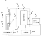
- FIG. 1 is a configuration diagram showing a power converter according to Embodiment 1;
- FIG. It is a circuit diagram which shows the main circuit by a full-bridge circuit.
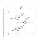
- 1 is a circuit diagram showing an example of a DC/DC converter;
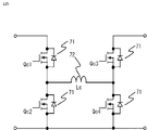
- FIG. 1 is a circuit diagram showing an example of a DC/DC converter;
- FIG. 1 is a configuration diagram showing a power converter according to Embodiment 1;
- FIG. 1 is a configuration diagram showing a power converter according to Embodiment 1;
- FIG. 1 is a configuration diagram showing a power converter according to Embodiment 1;
- FIG. 1 is a configuration diagram showing a power converter according to Embodiment 1;
- FIG. 1 is a configuration diagram showing a power converter according to Embodiment 1;
- FIG. 1 is a configuration diagram showing a power converter according to Embodiment 1;
- FIG. 1 is a configuration
- FIG. 1 is a configuration diagram showing a power converter according to Embodiment 1;
- FIG. 4 is a diagram showing operation waveforms of the power conversion device according to Embodiment 1;
- FIG. 1 is a configuration diagram showing a power converter according to Embodiment 1;
- FIG. 1 is a configuration diagram showing a power converter according to Embodiment 1;
- FIG. 10 is a configuration diagram showing a power conversion device according to Embodiment 2;
- 1 is a circuit diagram showing a circuit composed of an inductance, a capacitance and a load resistance;
- FIG. FIG. 3 is a circuit diagram showing a circuit in which a resistance component is connected in series with a capacitance and composed of an inductance, a capacitance, and a load resistance;
- FIG. 11 is a circuit diagram showing a voltage adjustment circuit in a power conversion device according to Embodiment 3;
- FIG. 11 is a circuit diagram showing a voltage adjustment circuit in a power conversion device according to Embodiment 3;
- FIG. 11 is a circuit diagram showing a voltage adjustment circuit in a power conversion device according to Embodiment 3;
- FIG. 11 is a circuit diagram showing a voltage adjustment circuit in a power conversion device according to Embodiment 3;
- FIG. 11 is a configuration diagram showing a control circuit in a power conversion device according to Embodiment 4;
- FIG. 11 is a configuration diagram showing a control circuit in a power conversion device according to Embodiment 4;
- FIG. 11 is a configuration diagram showing a control circuit in a power conversion device according to Embodiment 4;
- FIG. 11 is a configuration diagram showing a power conversion device according to Embodiment 5;
- FIG. 12 is a diagram showing changes in state in the power conversion device according to Embodiment 6; It is a figure which shows the time-dependent change of the gate voltage applied to a switching element.
- Embodiment 1 The present application relates to the field of power electronics.
- 1 and 2 are configuration diagrams showing a power converter according to Embodiment 1.
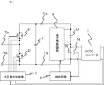
- FIG. The power converter according to Embodiment 1 includes a main circuit 2 , a main circuit controller 3 , and a main circuit power feeder 4 .
- a main circuit 2 is composed of main circuit switching elements Q1 and Q2 and a main circuit storage element 1 .
- the main circuit controller 3 controls the main circuit switching elements Q1 and Q2.
- the main circuit power supply device 4 supplies control power from the main circuit power storage element 1 to the main circuit control device 3 . As shown in FIG.
- the main circuit power supply device 4 includes a plurality of voltage dividing power storage elements 5A and 5B connected in series, a voltage adjustment circuit 6, one or more DC/DC converters 7, and a control circuit 8.
- the voltage adjustment circuit 6 is connected to the plurality of voltage-dividing storage elements 5A and 5B, and the voltage of the plurality of voltage-dividing storage elements 5A and 5B is adjusted by the transfer of electric power between the plurality of voltage-dividing storage elements 5A and 5B. adjust each.
- the DC/DC converter 7 is connected to one voltage-dividing storage element 5B among the plurality of voltage-dividing storage elements 5A and 5B, and supplies control power.
- the control circuit 8 controls the voltage adjustment circuit 6 by outputting two patterns of control command values.
- the power converter includes a main circuit 2 comprising a main circuit storage element 1 and main circuit switching elements Q1 and Q2, a main circuit controller 3 for driving and controlling the main circuit switching elements Q1 and Q2, and a main circuit storage element 1. and a main circuit power supply device 4 that supplies power to the main circuit control device 3 .
- the main circuit 2 shown in FIG. 1 is a so-called half-bridge circuit, but a different form of the main circuit is shown in FIG.
- the main circuit shown in FIG. 3 is a so-called full bridge circuit.
- the main circuit shown in FIG. 1 or 3 is one unit converter used in MMC (Modular Multilevel Converter). As a configuration of the unit converter, there is a half-bridge cell shown in FIG.
- the main circuit 2 has terminals TCa and TCb for connecting to other unit converters.
- the configuration of the main circuit 2 is not limited to the purpose and application as long as it is a circuit that includes the main circuit storage element 1 and converts the voltage and energy of the main circuit storage element 1 into power by the main circuit switching element Q1 or the like. Any circuit may be used. At that time, the number of main circuit switching elements and the types and numbers of other elements are not limited.
- the main circuit power supply device 4 is configured to supply power from the main circuit power storage element 1 to the main circuit control device 3 .
- the main circuit controller 3 has a gate drive circuit 31 and a control signal generation circuit 32 .
- the gate drive circuit 31 drives the main circuit switching elements Q1 and Q2, and the control signal generation circuit 32 supplies the gate drive circuit 31 with drive signals.
- the main circuit control device 3 is composed of a gate drive circuit 31 and a control signal generation circuit 32, but it is only an example of a device for driving the main circuit switching elements Q1 and Q2, and is not limited to the above configuration. do not have.
- the main circuit power supply device 4 includes a plurality of voltage dividing storage elements 5A and 5B connected in series, a voltage adjustment circuit 6 connected in parallel to the voltage dividing storage elements 5A and 5B, and a voltage dividing storage element 5B. It has a DC/DC converter 7 that outputs electric power from the power storage elements 5A and 5B to the main circuit controller 3 .
- a control circuit 8 in the main circuit power supply device 4 outputs a control command value to the voltage adjustment circuit 6 to control the voltage adjustment circuit 6 .
- the voltage adjustment circuit 6 has three or more connection terminals, is connected to two or more voltage dividing storage elements, and transmits and receives electric power between the voltage dividing storage elements.
- the DC/DC converter 7 receives at least one voltage-dividing power storage element and outputs a desired voltage to the main circuit control device 3 .
- the voltage adjustment circuit 6 adjusts the voltage balance between two or more voltage-dividing power storage elements connected in series as described above, and does not require insulation using a transformer, and the circuit system is simple. , miniaturization can be achieved.
- a plurality of insulated power supplies are connected in series, and each insulated power supply uses a transformer.
- the DC/DC converter 7 may adopt any circuit system. If insulation between input and output is not required, for example, a chopper method can be used. If insulation between input and output is required, for example, a flyback system with a transformer can be used. In the main circuit power supply system of the present embodiment, the potential between the input and output is the same, so insulation is not required unless there is a special request or reason. Even if insulation is necessary for some reason, the input of the DC/DC converter 7 is voltage-divided by the voltage-dividing power storage elements 5A and 5B and the voltage regulation circuit 6 as described above, and the voltage is reduced.
- FIG. 4 shows a case where the DC/DC converter 7 is of a chopper type and corresponds to a range ratio for step-down operation. 72 (Lc).
- FIG. 4 shows a case where the DC/DC converter 7 is of a chopper type and corresponds to a range ratio for step-down operation. 72 (Lc).
- FIG. 5 shows the case corresponding to the ratio of the range including the step-down operation and the step-up operation. It is The circuit configuration shown in FIG. 4 is simpler. Also, the control configuration is more complicated in the case of supporting both the step-up operation and the step-down operation than in the case of supporting only the step-down operation.
- the voltage adjustment circuit 6 adjusts the voltage balance of two or more voltage-dividing storage elements according to the control command value output from the control circuit 8 .
- control is performed so that the on-time and off-time of switching elements, which are components of the voltage adjustment circuit, are set to 50% each.
- Providing a command value to a voltage regulation circuit is disclosed.
- the voltage balance between the two voltage-dividing power storage elements connected in series is kept equal by 50% each. Fixing the control command value to a value of 50% makes it possible to avoid complicating the controller in the method of finely adjusting the control command value.
- a combination of an amplifier or an integrator proportional integral control
- a new control command value is set to bring the voltage of one of the two or more voltage-dividing storage elements to which the voltage adjustment circuit 6 is connected to approach zero voltage. .
- This implements the following operations.
- two voltage dividing storage elements 5A and 5B are installed, and the voltage of the main circuit storage element 1 is divided by the two voltage dividing storage elements 5A and 5B.
- a DC/DC converter 7 is connected to the voltage-dividing storage element 5B, which is located on the lower side of the two voltage-dividing storage elements 5A and 5B, and is configured to supply power to the main circuit control device 3. .
- the voltage adjustment circuit 6 is connected in parallel to the two voltage dividing power storage elements 5A and 5B that are connected in series.
- a control command value of 50% when a control command value of 50% is output from the control circuit 8 to the voltage adjustment circuit 6, the voltages of the two voltage-dividing storage elements 5A and 5B are substantially equally divided. However, voltage imbalance may occur due to factors such as component variation or component loss.
- the control circuit 8 outputs a control command value of 100% to the voltage adjustment circuit 6 .
- the voltage of the upper voltage-dividing energy storage element 5A of the two voltage-dividing energy storage elements 5A and 5B connected in series becomes zero voltage
- the lower voltage-dividing energy storage element 5B becomes zero voltage.
- the voltage of the main circuit storage element 1 is all applied. Therefore, a control command value of 100% is defined as a bypass control command value. That is, the bypass control command value is a control command value for bypassing at least one voltage dividing power storage element among the plurality of voltage dividing power storage elements.
- the input voltage of the DC/DC converter 7 is approximately the voltage of the main circuit storage element 1. equal to
- the voltage adjustment circuit 6 is operated with a control command value of 50% as disclosed in Patent Document 2
- the voltage of the lower voltage-dividing storage element 5B is approximately 50% of the voltage of the main circuit storage element 1.
- a control command value of 50% is defined as a control command value for voltage division. That is, the voltage dividing control command value is a control command value for dividing the voltage of the main circuit storage element 1 among a plurality of voltage dividing storage elements.
- the reason why it is set to approximately 50% is that, strictly speaking, it deviates from 50% due to factors such as variations in components. Therefore, by selecting either 50% (control command value for voltage division) or 100% (control command value for bypass) as the control command value, the input voltage of DC/DC converter 7 is The voltage can be 50% or 100% of the voltage.
- the voltage of the main circuit storage element 1 fluctuates greatly, when the voltage of the main circuit storage element 1 is high, 50% (control command value for voltage division) is selected as the control command value, and the voltage of the main circuit storage element 1 is is low, by selecting 100% (control command value for bypass) as the control command value, the fluctuation range of the input voltage of the DC/DC converter 7 can be suppressed.
- the divided voltage of the voltage dividing power storage elements 5A and 5B also fluctuates so as to follow it. You can choose.
- the voltage target value of the main circuit storage element 1, which is internal information of the main circuit control device 3, is communicated. It is conceivable to notify the control circuit 8 by some means.
- a method of detection there is a method of notifying the detected value from the main circuit control device 3 by communication or the like in the same manner as the voltage target value.
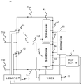
- a method of detecting by the control circuit 8 of the main circuit power supply device 4 As the latter method, as shown in FIG. 7, a voltage detector 108 for detecting the voltage of the main circuit storage element 1 is connected to the control circuit 8 .
- a method of detecting the voltage there is a method of dividing the voltage by a resistor having a large resistance value and detecting the divided voltage with an insulation amplifier, a voltage sensor, or the like, but other methods may be used.
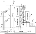
- FIG. 8 is a configuration diagram of a power conversion device including a main circuit power supply device having four voltage dividing power storage elements.
- the four voltage dividing power storage elements are 5A, 5B, 5C, and 5D in order from the high potential side (upper side).
- a DC/DC converter 7 is connected in parallel with one or more of the four voltage dividing storage elements 5A, 5B, 5C and 5D.
- the DC/DC converter 7 is connected in parallel with the voltage dividing power storage element 5D at the lowest stage to supply electric power to the main circuit control device 3 .
- the voltage adjustment circuit 6C is connected in parallel to both the lowermost voltage-dividing storage element 5D and the voltage-dividing storage element 5C adjacent to the lowermost voltage-dividing storage element 5D, whereby the voltage-dividing storage element 5C and voltage dividing storage element 5D.
- a voltage adjustment circuit 6B is connected in parallel to both the voltage-dividing storage element 5B and the voltage-dividing storage element 5C on the opposite side of the voltage-dividing storage element 5D with respect to the voltage-dividing storage element 5C. As a result, the voltage balance between the voltage-dividing storage element 5C and the voltage-dividing storage element 5B is adjusted.
- a voltage adjustment circuit 6A is connected in parallel to both the voltage dividing storage element 5B and the voltage dividing storage element 5A to adjust the voltage balance between the voltage dividing storage element 5A and the voltage dividing storage element 5B.
- the voltage adjusting circuits 6A, 6B, 6C By connecting the voltage adjusting circuits 6A, 6B, 6C to the voltage dividing storage elements 5A, 5B, 5C, 5D connected in series as described above, the voltage dividing storage elements 5A, 5B, 5C, Voltage balance between up to 5D can be adjusted.
- a control command value is sent from the control circuit 8 to the voltage adjustment circuits 6A, 6B, and 6C of each stage.
- a control command value of 50% (control command value for voltage division) is sent to the voltage adjustment circuits 6A, 6B, and 6C in all stages, the voltage of the main circuit power storage element 1 is changed to all series-connected voltage division voltages.
- the voltage is divided equally by the storage elements 5A, 5B, 5C, and 5D.
- the four voltage dividing storage elements 5A, 5B, 5C, and 5D connected in series divide the voltage of the main circuit storage element 1 by 4 with a control command value of 50% (voltage dividing control command value).
- the control command value for the voltage adjustment circuit connected to the voltage dividing storage element to which the DC/DC converter 7 is connected is 50% (voltage dividing control command value).
- the connection position farthest from the voltage-dividing storage element 5D among the series-connected voltage-dividing storage elements is In the voltage adjustment circuit 6A connected to the uppermost voltage dividing storage element 5A, first, a control command value of 100% (bypass control command value) is selected. After that, the voltage adjustment circuit 6B connected to the voltage dividing storage element 5B at the connection position (the second in the upper row) close to the voltage dividing storage element 5A in the uppermost stage, and the control command value of 100% (bypass control command value).
- FIG. 9 is a configuration diagram showing the operation when only the control command value given to the voltage adjustment circuit 6A connected to the uppermost voltage dividing storage element 5A is set to 100% (control command value for bypass).
- Vm be the main voltage of the main circuit storage element 1 .
- the control command value of the voltage adjustment circuit 6A connected to the uppermost voltage dividing energy storage element 5A and the lower voltage dividing energy storage element 5B is set to 100%. (bypass control command value), and the voltage of the uppermost voltage-dividing storage element 5A is set to zero volts.
- the control command value for the remaining voltage adjusting circuits 6B and 6C connected to the voltage dividing power storage elements 5B, 5C and 5D is assumed to be 50% (voltage dividing control command value).
- the main voltage Vm is equally divided by the three voltage-dividing storage elements 5B, 5C, and 5D, and each voltage of the voltage-dividing storage elements 5B, 5C, and 5D is set to Vm/3. It should be noted that each voltage value is an approximate value, and the actual value may slightly deviate due to various factors of variation.
- FIG. 10 is a configuration diagram showing the operation of setting the voltages of the uppermost voltage-dividing storage element 5A and the voltage-dividing storage element 5B one step below the uppermost stage to zero volts.
- the control command value given to the voltage adjustment circuit 6A connected to the voltage dividing storage element 5A in the uppermost stage and the voltage dividing storage element 5B one step below the uppermost stage is 100% (control instruction value for bypass).
- control command value given to the voltage adjustment circuit 6B connected to the voltage dividing storage element 5B one step below the top and the voltage dividing storage element 5C two steps below the top is set to 100% (bypass control command value). and
- the voltage adjustment circuit 6A operates so as to transfer the energy of the voltage-dividing storage element 5A to the voltage-dividing storage element 5B so that the voltage of the voltage-dividing storage element 5A at the top becomes zero volts.
- the voltage adjustment circuit 6B operates so as to move the energy of the voltage-dividing storage element 5B to the voltage-dividing storage element 5C one step below the voltage-dividing storage element 5B. Therefore, the voltage of the voltage-dividing storage element 5A at the top and the voltage of the voltage-dividing storage element 5B one step below the top become zero volts. Then, the main voltage Vm of the main circuit storage element 1 is equally divided by the remaining voltage-dividing storage elements 5C and 5D, and the divided voltage values of the voltage-dividing storage elements 5C and 5D become Vm/2.
- the vertical axis indicates voltage and the horizontal axis indicates time. Although the values on the vertical axis are small values, they are only examples, and if they are viewed as magnifications relative to the reference values, they match the actual results.
- the main voltage of the main circuit storage element 1 is indicated by a dotted line as Vm.
- the voltage of the voltage-dividing storage element 5A is indicated by a two-dot chain line as V5A.
- the voltage of the voltage-dividing storage element 5B is indicated by a one-dot chain line as V5B.
- the voltage of the voltage-dividing storage element 5C is indicated by a dashed line as V5C.
- the voltage of the voltage-dividing storage element 5D is indicated by a solid line as V5D.
- the control circuit 8 sets the control command value of each stage to 100% (control command value for bypass) or 50% (
- the waveform of FIG. 11 is generated by selecting from the control command value for voltage division).
- the control command value of the voltage adjustment circuit 6A connected to the voltage dividing storage element 5A becomes 100% (control command value for bypass) at time t1.
- the voltage division ratio of the main voltage Vm of the main circuit storage element 1 increases in the voltages V5B, V5C, and V5D. Therefore, the voltages V5B, V5C, and V5D turn to increase.
- the control command value for the voltage adjustment circuit 6B connected to the voltage-dividing storage element 5B becomes 100 at time t2. % (control command value for bypass).
- the control command value for the voltage adjustment circuit 6C connected to the voltage-dividing storage element 5C is set at time t3. It is 100% (control command value for bypass).
- any logic may be used as the logic for selecting the control command value installed in the control circuit 8, but as one example, the main voltage Vm is detected and the voltage dividing power storage element as circuit configuration information is stored.
- the circuit configuration information may be information specifying the number of stages of capacitors connected in series.
- the voltage of a voltage-dividing storage element for example, the voltage of a voltage-dividing storage element connected to the DC/DC converter 7 .
- the second logic example requires less or no circuit configuration information.
- 12 and 13 are configuration diagrams in the case of using the voltage of the storage element for voltage division. In FIGS. 12 and 13, the voltage of the voltage-dividing storage element is detected by a voltage detector 51 and input to the control circuit 8 .
- the voltage-dividing power storage elements 5A and 5B and the voltage adjustment circuit 6 do not require insulation and can be miniaturized.
- the output DC/DC converter 7 basically does not require insulation.
- the control command value of the voltage adjustment circuit 6 may be two patterns of fixed values, it is possible to obtain the effect of simplifying the control configuration.
- FIG. 14 is a configuration diagram showing a power converter according to Embodiment 2.
- This embodiment is for increasing the stability of the operation of the main circuit power supply device 4 .
- resistance components 9A, 9B, 9C, and 9D are added in series with the voltage dividing power storage elements 5A, 5B, 5C, and 5D in the main circuit power supply device 4 .
- the resistance components 9A, 9B, 9C, and 9D include, for example, resistors or wiring resistance, high-frequency resistance elements using a magnetic material such as ferrite, and the like. Since the main circuit power supply device 4 or the voltage adjustment circuit 6 shown in Embodiment 1 includes wiring or a current-limiting reactor, it includes an inductance component.
- the voltage-dividing storage element 5 includes a capacitance from its role.
- the main circuit control device 3 Since power is supplied to the main circuit control device 3, the main circuit control device 3 becomes a load when viewed from the main circuit power supply device 4, and the power supplied to the main circuit control device 3 can be simply regarded as a resistance component.
- the power consumption of the main circuit controller 3 is generally mainly due to the driving power of the main circuit switching elements Q1 and Q2. It can be regarded as the power consumption by the resistance component. Therefore, power to a portion of the voltage dividing storage element, the voltage adjustment circuit 6, and the main circuit controller 3 side of the main circuit power supply device 4 can be replaced with a circuit composed of an inductance, a capacitance, and a load resistance.
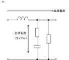
- FIG. 15 shows a circuit consisting of such an inductance, capacitance and load resistance.
- FIG. 15 does not include resistance components 9A, 9B, 9C, and 9D connected in series with the voltage-dividing storage element 5 shown in FIG.
- FIG. 15 shows a circuit in which an inductance is connected in series to a parallel circuit of load resistance and capacitance, and the capacitance and inductance form a series circuit. Furthermore, if the storage elements for voltage division and the voltage adjustment circuits of the main circuit power supply device 4 are configured in multiple stages, the series circuit of the capacitance and the inductance in the circuit of FIG. 15 becomes multiple stages.
- a series circuit of capacitance (capacitor) and inductance (coil) is a resonant circuit, so the voltage (current) resonates.
- the control circuit 8 uses a digital circuit such as a microcomputer or a digital signal processor, or an analog circuit such as an analog divider or an analog amplifier.
- the purpose is to reduce the number of parts by simplifying the configuration of the control circuit 8. Therefore, the damping control by the above-described digital circuit or analog circuit is contrary to the purpose. The number of parts tends to increase. Therefore, as shown in FIG.
- a resistance component 9 is connected in series with a voltage-dividing storage element (capacitance) to form a circuit composed of an inductance, a capacitance, and a load resistance.
- a resistance component 9 is added in series with the capacitance. Since the resistance component 9 serves as a damping element (damping element), resonance is suppressed. Therefore, there is no need to apply damping control by digital or analog circuits.
- the control circuit 8 does not need to provide damping control. , the number of parts can be reduced and the operation can be stabilized.
- the addition of the resistance components 9A, 9B, 9C, and 9D also adds losses caused by the resistance components 9A, 9B, 9C, and 9D, which may reduce the conversion efficiency of the main circuit power supply device 4. may be of concern.
- the conversion efficiency is output power ⁇ input power ⁇ 100%, which can be rewritten as (input power ⁇ loss) ⁇ input power ⁇ 100%.
- the main circuit power supply device 4 that supplies control power from the main circuit storage element 1 to the main circuit control device 3 the power from the main circuit storage element 1 to the main circuit power supply device 4 becomes the input power.
- the power from the main circuit power supply device 4 to the main circuit control device 3 is the output power.
- the resistance components 9A, 9B, 9C, and 9D are connected in series with the voltage-dividing storage elements 5A, 5B, 5C, and 5D, there is a concern that the conversion efficiency will decrease for the reason described later. can be eliminated or reduced. That is, in the main circuit control device 3 to which power is supplied from the main circuit power supply device 4, drive power is mainly supplied to the main circuit switching elements Q1 and Q2, and the power is substantially constant. That is, the power supplied by the main circuit power supply device 4 is approximately DC power, and the flowing current is DC current.
- the impedance components included in the main circuit power supply device 4 include the capacitances of the voltage dividing power storage elements 5A, 5B, 5C, and 5D and the voltage adjustment circuit 6, except for the resistance components 9A, 9B, 9C, and 9D. Inductance and DC current pass through the inductance.
- ripples generated during power fluctuations or by switching operations of the switching elements 61 and 71 (see FIGS. 4 and 5) pass through the voltage dividing storage elements 5A, 5B, 5C and 5D. Therefore, by connecting the resistance components 9A, 9B, 9C, and 9D in series with the voltage dividing storage elements 5A, 5B, 5C, and 5D, the ripple (alternating current) also passes through the resistance components 9A, 9B, 9C, and 9D. , resistance components 9A, 9B, 9C, and 9D.
- the impedance of capacitance (1/j ⁇ C) is inversely proportional to frequency
- the impedance of inductance (j ⁇ L) is proportional to frequency.
- the power of the main circuit control device 3 is the driving power of the main circuit switching elements Q1 and Q2, and is normally constant, so power fluctuations occur less frequently. Therefore, ripples (alternating currents) generated by power fluctuations or switching operations of the switching elements 61 and 71 pass through the resistance components 9A, 9B, 9C and 9D, and losses occur in the resistance components 9A, 9B, 9C and 9D. less frequently. Therefore, if the frequency of loss caused by the resistance components 9A, 9B, 9C, and 9D is low, the effect of the resistance components 9A, 9B, 9C, and 9D on the conversion efficiency is small.
- a ripple caused by the switching operation of the switching elements 61 and 71 always occurs while the main circuit power supply device 4 is in operation.
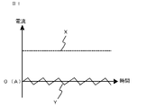
- the amplitude of the voltage can be reduced.
- the voltage amplitude can be reduced by setting the switching frequency high, because the voltage amplitude is proportional to the energization time.
- the magnitude of the alternating current (ripple) indicated by the solid line Y can be sufficiently reduced. If a resistance component is connected in series with the inductance, a DC current loss will occur.
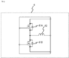
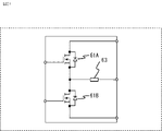
- FIG. 19 is a diagram showing the configuration of the voltage adjustment circuit, showing an example of the configuration in which the voltage balance is adjusted by being connected in parallel with two adjacent voltage dividing power storage elements.
- FIG. 19 is composed of a half-bridge circuit in which two switching elements 61A and 61B are connected in series, and a reactor 62 as a current-limiting element connected to the midpoint of the half-bridge circuit.
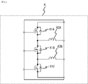
- FIG. 20 is a diagram showing the configuration of another voltage regulating circuit, showing a voltage regulating circuit 6 connected in parallel with three voltage-dividing storage elements.
- FIG. 20 includes three switching elements 61A, 61B, 61C connected in series, two reactors 62A, 62B connected between the switching elements 61A, 61B, 61C, and four terminals.
- a reactor is often used as the current-limiting element, but a resistor 63 can also be used as the current-limiting element, as shown in FIG. In this case, the slope of the current is limited by the wiring inductance, the parasitic inductance, or the switching speed of the switching element 61.
- the upper switching element 61A is always on.
- a voltage (named differently depending on the type of element, such as gate-source voltage, gate-emitter voltage, or base-emitter voltage) is applied.
- the voltage dividing storage element connected in parallel with the upper switching element 61A via the current limiting element 62 has a voltage of zero volts if the upper switching element 61A is always on.
- the upper switching element 61A and the lower switching element 61B are alternately turned on (or off) at a one-to-one time ratio. That is, the two switching elements 61A and 61B are alternately turned on for the same period of time.
- the two voltage dividing power storage elements connected in parallel with the two switching elements 61A and 61B have the same voltage because the switching elements 61A and 61B are turned on via the current limiting element 62 for the same period of time.
- the main circuit control device 3 which is the load of the main circuit power supply device 4
- the DC current is superimposed on the current limiting element 62, so that they do not have the same voltage.
- the voltage also varies due to variations in components.
- the rated voltage of each component is set in stages such as 100V, 300V, 600V, 900V, 1200V, etc. It's not something that goes up. For example, a maximum working voltage of 50V and a maximum working voltage of 70V can both be handled by parts with a rated voltage of 100V.
- the voltage of the storage element for voltage division is detected, and the control command value 50% (control command value for voltage division) is corrected to equalize the respective voltages.
- Adopting such a correction method requires the addition of a detector such as a voltage sensor, which conflicts with reducing the number of parts.
- a detector such as a voltage sensor
- an idle period is provided during which the two switching elements 61A and 61B are turned off simultaneously so that the upper and lower switching elements 61A and 61B are not turned on at the same time to cause a short circuit.
- a dead time is actually employed, but since it does not affect the description of the embodiment, it is assumed that there is no dead time.
- the voltage adjustment circuit 6 is configured by a circuit including two or more switching elements and one or more current limiting elements. As a result, the voltage of the voltage-dividing power storage element can be adjusted using only approximately two patterns of control command values, and the configuration of the power converter can be simplified.
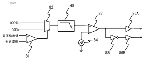
- FIG. 22 is a block configuration diagram showing a control circuit.
- Selector 82 selects either one of the control command value of 100% (control command value for bypass) and the control command value of 50% (control command value for voltage division). The aforementioned correction value may be superimposed on the control command value.
- the selector switching condition uses the result of the comparator 81 judging the magnitude of the detected voltage value and the judgment threshold. For example, if the detected voltage value is smaller than the determination threshold, the control command value of 100% (control command value for bypass) is selected; value).
- the voltage detection value is either the main voltage of the main circuit storage element 1 or the voltage of the voltage dividing storage element 5 and is obtained by voltage detectors 108 and 51 .
- the determination threshold is individually set for each voltage adjustment circuit 6 that is the target of the control command value. However, when the voltage of the voltage-dividing storage element 5 is used as the voltage detection value, the determination threshold may be the same value.
- One of the selected control command values is subjected to PWM (PULSE WIDTH MODULATION) by determining the magnitude of the carrier wave 84 and the comparator 83 .
- PWM PULSE WIDTH MODULATION
- the two-level signal is branched and one signal is sent to one switching element 61A via the driver 86A.
- the other signal is sent through a NOT circuit (inverter) or an inverting amplifier circuit 85 and then through a driver 86B to the other switching element 61B.
- the two switching elements 61A and 61B are alternately turned on or off.
- FIG. 23 is a block diagram showing a control circuit for avoiding such a situation.
- time change limiting means 87 limits the time change of the selected control command value.
- the control command value change (dV) per fixed time (dt) of the control command value exceeds the limit value (dVmax)
- the output of the time change limiting means 87 is the control command value per fixed time (dt).
- the control command value is set such that the control command value change (dV) is limited (overwritten) by the limit value (dVmax).
- the time change limiting means 87 is called a dV/dt limiter (inclination limiter).
- the time change limiting means 87 by the dV/dt limiter has the effect of replacing the step change of the control command value with a staircase change (ramp change).
- a staircase change staircase change
- the time change limit by the dV/dt limiter does not act on minute signal changes in the correction value of the control command value by feedback control. It does not affect control response. Because the dV/dt limiter is a so-called limiter, it limits large signals that exceed the limit value, and conversely allows minute signals that do not exceed the limit value to pass without limiting. Therefore, the use of the dV/dt limiter, which is the time change limiter 87, has little effect on feedback control.
- a method other than the dV/dt limiter, which is the time change limiter 87, can be applied if the influence on the feedback control is taken into consideration. For example, it is conceivable to apply a low-pass filter that obtains a desired frequency response to moderate the time change of the control command value.
- FIG. 24 is a block configuration diagram showing a control circuit when a low-pass filter 88 is used instead of the time change limiting means 87.
- a low-pass filter 88 is used instead of the time change limiting means 87.
- FIG. 25 is a configuration diagram showing a power converter according to Embodiment 5.
- the resistance component 9 is connected in series with the voltage-dividing storage element 5 in order to suppress resonance due to disturbance.
- the main circuit control device 3 which is the load of the main circuit power supply device 4 consumes substantially constant power (DC power).
- the voltage adjustment circuit 6 is basically operated with two patterns of control command values of 50% (control command value for voltage division) and 100% (control command value for bypass). From the above, the disturbance to be assumed in the main circuit power supply device 4 is caused by fluctuations in the main voltage of the main circuit power storage element 1 on the input side, not on the load side.
- a case where the main voltage of the main circuit power storage element 1 fluctuates corresponds to the time when the power converter is started.
- a sequence is assumed in which initial charging is performed until the main voltage reaches the steady operating voltage from a zero volt state, and after reaching the steady operating voltage, the system shifts to steady operation. Therefore, it is assumed that the period during which the main circuit power supply device 4 needs to suppress resonance due to disturbance is limited to the start-up of the power conversion device.
- the resistance components 9A, 9B, 9C, and 9D connected in series with the voltage dividing power storage elements 5A, 5B, 5C, and 5D may be short-circuited (bypassed) except when the power converter is started. become.
- FIG. 25 shows a power converter with additional short circuit means 10A, 10B, 10C and 10D for bypassing the resistance components 9A, 9B, 9C and 9D.
- the completion of the start-up of the power converter is sensed by some means, for example, by detecting the main voltage of the main circuit storage element 1, and the short-circuit means 10A, 10B, 10C, 10D bypassing the resistance components 9A, 9B, 9C, 9D. throw into.
- the resistance components 9A, 9B, 9C, and 9D are bypassed, the loss of the entire device can be reduced by the loss caused by the resistance components 9A, 9B, 9C, and 9D, further increasing the conversion efficiency. can be done.
- Embodiment 6 a method for suppressing resonance in the main circuit power supply device 4 will be described.
- the connection of resistance component 9 in series with voltage-dividing storage element 5 in order to suppress resonance due to disturbance has been described.
- the resonance is suppressed by changing the gate voltage of the switching element 61 (see FIGS. 19 to 21).
- a switching element 61 such as a MOSFET (METAL OXIDE SEMICONDUCTOR FIELD EFFECT TRANSISTOR) or an IGBT (INSULATED GATE BIPOLAR TRANSISTOR) has a low on-resistance (on-voltage) between the drain and source (between the collector and the emitter) when the gate voltage is increased even in the same individual. On the contrary, when the gate voltage is lowered, the on-resistance (on-voltage) increases. By changing the gate voltage in this manner, the same effect as increasing or decreasing the resistance component can be obtained.
- MOSFET METAL OXIDE SEMICONDUCTOR FIELD EFFECT TRANSISTOR
- FIG. 26A is a diagram showing changes in state in the power converter according to Embodiment 6
- FIG. 26B is a diagram showing changes over time in gate voltages applied to switching elements.
- the gate voltage that drives the switching element 61 of the voltage adjustment circuit 6 is lowered, and the gate voltage is set to a steady value except when the power converter is started. set it back to This makes it possible to suppress voltage and current oscillations in each part of the main circuit power supply device 4 without connecting a resistance component in series with the voltage-dividing storage element.
Landscapes
- Engineering & Computer Science (AREA)
- Power Engineering (AREA)
- Dc-Dc Converters (AREA)
- Inverter Devices (AREA)
Abstract
Description
また、特許文献2の開示回路は、直列コンデンサの電圧に関して、複数の電圧調整回路によって制御するが、入力電圧が低下したときには電圧制御回路と電圧検出回路を用いて、スイッチングパターンを変化させて直流コンデンサ電圧を制御するようになっている。この方法ではスイッチングパターンを変化させる電圧制御回路として、例えば比例積分制御などの手段が必要となり、制御回路が複雑化するという問題がある。
主回路スイッチング素子と主回路蓄電要素とを備える主回路と、
前記主回路スイッチング素子を制御する主回路制御装置と、
前記主回路蓄電要素から前記主回路制御装置へ制御電力を供給する主回路給電装置を備え、
前記主回路給電装置は、直列接続された複数の分圧用蓄電要素と、
前記複数の分圧用蓄電要素に接続され、前記複数の分圧用蓄電要素間の電力の授受により、前記複数の分圧用蓄電要素の電圧をそれぞれ調整する電圧調整回路と、
前記複数の分圧用蓄電要素のうち、少なくとも1個の前記分圧用蓄電要素に接続され、前記主回路制御装置に前記制御電力を供給する少なくとも1個のDC/DCコンバータと、
前記主回路蓄電要素の電圧を前記複数の分圧用蓄電要素間で分割させる分圧用の制御指令値、および前記複数の分圧用蓄電要素のうちの少なくとも1つの前記分圧用蓄電要素をバイパスさせるバイパス用の制御指令値の2パターンの制御指令値を出力することにより前記電圧調整回路を制御して、前記DC/DCコンバータの入力電圧を調整する制御回路を備えるものである。
主回路スイッチング素子および主回路蓄電要素を含む主回路と、前記主回路スイッチング素子を制御する主回路制御装置とを備える電力変換装置に設けられ、前記主回路蓄電要素から前記主回路制御装置へ制御電力を供給するものであって、
直列接続された複数の分圧用蓄電要素と、
前記複数の分圧用蓄電要素に接続され、前記複数の分圧用蓄電要素間の電力の授受により、前記複数の分圧用蓄電要素の電圧をそれぞれ調整する電圧調整回路と、
前記複数の分圧用蓄電要素のうち、少なくとも1個の前記分圧用蓄電要素に接続され、前記主回路制御装置に前記制御電力を供給する少なくとも1個のDC/DCコンバータと、
前記主回路蓄電要素の電圧を前記複数の分圧用蓄電要素間で分割させる分圧用の制御指令値、および前記複数の分圧用蓄電要素のうちの少なくとも1つの前記分圧用蓄電要素をバイパスさせるバイパス用の制御指令値の2パターンの制御指令値を出力することにより前記電圧調整回路を制御して、前記DC/DCコンバータの入力電圧を調整する制御回路を備えるものである。
本願はパワーエレクトロニクス分野に関するものである。図1、図2は実施の形態1に係る電力変換装置を示す構成図である。実施の形態1による電力変換装置は、主回路2と、主回路制御装置3と、主回路給電装置4を備えている。主回路2は主回路スイッチング素子Q1、Q2と主回路蓄電要素1により構成されている。主回路制御装置3は主回路スイッチング素子Q1、Q2を制御する。主回路給電装置4は主回路蓄電要素1から主回路制御装置3に制御電力を供給する。
図2に示すように、主回路給電装置4は、直列接続された複数の分圧用蓄電要素5A、5Bと、電圧調整回路6と、1つ以上のDC/DCコンバータ7と、制御回路8とを備える。電圧調整回路6は複数の分圧用蓄電要素5A、5Bに接続されるものであり、複数の分圧用蓄電要素5A、5Bの間における電力の授受により、複数の分圧用蓄電要素5A、5Bの電圧をそれぞれ調整する。DC/DCコンバータ7は、複数の分圧用蓄電要素5A、5Bのうち、1つの分圧用蓄電要素5Bに接続され、制御電力を供給するものである。制御回路8は、2パターンの制御指令値を出力することで電圧調整回路6を制御するものである。
図6に示す主回路給電装置4においては、2つの分圧用蓄電要素5A、5Bが設置され、主回路蓄電要素1の電圧を2つの分圧用蓄電要素5A、5Bで分圧するものである。また、2つの分圧用蓄電要素5A、5Bのうち下側に存在する分圧用蓄電要素5BにDC/DCコンバータ7が接続され、主回路制御装置3に電力の供給を行うように構成されている。電圧調整回路6は、直列接続される2つの分圧用蓄電要素5A、5Bに対して並列に接続されている。
図8は4つの分圧用蓄電要素を有する主回路給電装置を含む電力変換装置の構成図である。4つの分圧用蓄電要素を高電位側(上側)から順番にそれぞれ5A、5B、5C、5Dとする。4つの分圧用蓄電要素5A、5B、5C、5Dのうち1つ以上の分圧用蓄電要素と並列にDC/DCコンバータ7を接続する。ここでは最下段の分圧用蓄電要素5Dと並列にDC/DCコンバータ7を接続して、主回路制御装置3へ電力を供給する場合を示している。
以上より実施の形態1は、分圧用蓄電要素5A、5Bと電圧調整回路6は絶縁が不要であり小型化が図れる。又出力のDC/DCコンバータ7は基本的に絶縁が不要であり、絶縁が必要であっても入力と出力の電圧差が小さいことから小型化が図れる。更に電圧調整回路6の制御指令値は2パターンの固定値で良いことから制御構成が簡易となるという効果を得ることができる。
図14は実施の形態2による電力変換装置を示す構成図である。本実施の形態は、主回路給電装置4の動作の安定度を増すためのものである。図14において、主回路給電装置4における分圧用蓄電要素5A、5B、5C、5Dに対して直列に抵抗成分9A、9B、9C、9Dを追加している。抵抗成分9A、9B、9C、9Dとしては、例えば抵抗器又は配線による抵抗、更にはフェライトなどの磁性材を用いる高周波抵抗要素などがある。実施の形態1で示した主回路給電装置4もしくは電圧調整回路6は、配線又は限流用のリアクトルを備えているので、インダクタンス成分を含むことになる。分圧用蓄電要素5はその役割から静電容量を含む。
本実施の形態では、電圧調整回路6の構成について説明する。図19は電圧調整回路の構成を示す図であり、隣り合う2つの分圧用蓄電要素と並列に接続されて、電圧のバランスを調整する構成例を示している。図19において、2つのスイッチング素子61A、61Bが直列接続されたハーフブリッジ回路と、ハーフブリッジ回路の中点に接続される限流要素としてのリアクトル62とにより構成される。2つのスイッチング素子61A、61Bのオンとオフとを選択することで電流の経路を変えて、2つの分圧用蓄電要素の間の電圧のバランスを調整するものである。これにより簡易な回路構成で起動時又は変動時も支障なく動作する主回路給電装置4を提供することができる。
本実施の形態では、主回路給電装置4の制御回路8について説明する。制御回路8では制御指令値の選択を行うとともに、スイッチング素子61の駆動信号(ゲート電圧)の生成を行う。図22は制御回路を示すブロック構成図である。制御指令値100%(バイパス用の制御指令値)、および制御指令値50%(分圧用の制御指令値)のうち、いずれか一方をセレクタ82で選択する。制御指令値には前述の補正値を重畳しても良い。セレクタの切り替え条件は、電圧検出値と判定閾値との大小をコンパレータ81で判定した結果を用いる。例えば、電圧検出値が判定閾値よりも小さければ制御指令値100%(バイパス用の制御指令値)を選択し、電圧検出値が判定閾値よりも大きければ制御指令値50%(分圧用の制御指令値)を選択する。
dV/dtリミッタによる時間変化制限手段87は、制御指令値のステップ変化を、階段状の変化(ランプ変化)に置き換える作用を有する。
以上のように、時間変化制限手段87を追加することにより、主回路給電装置4内の各部の電圧及び電流の急変を抑制して安定化を図ることができる。
本実施の形態では、主回路給電装置4の変換効率を更に高める方法について説明する。図25は実施の形態5による電力変換装置を示す構成図である。上記においては、外乱による共振を抑制するために分圧用蓄電要素5と直列に抵抗成分9を接続することを説明した。また、主回路給電装置4の負荷である主回路制御装置3は概略一定の電力(直流電力)を消費することを説明した。さらに、電圧調整回路6は基本的に2パターンの制御指令値50%(分圧用の制御指令値)および100%(バイパス用の制御指令値)で動作させることを説明した。以上のことから主回路給電装置4における想定すべき外乱は、負荷側ではなくて入力側の主回路蓄電要素1の主電圧の変動が原因となる。
本実施の形態では、主回路給電装置4における共振を抑制する方法について説明する。上記実施の形態1から5において、外乱による共振を抑制するために分圧用蓄電要素5と直列に抵抗成分9を接続することに関して説明した。本実施の形態では、スイッチング素子61(図19~図21参照)のゲート電圧を変えることで共振を抑制するものである。MOSFET(METAL OXIDE SEMICONDUCTOR FIELD EFFECT TRANSISTOR)又はIGBT(INSULATED GATE BIPOLAR TRANSISTOR)などのスイッチング素子61は、同一個体においてもゲート電圧を高くするとドレインソース間(コレクタエミッタ間)のオン抵抗(オン電圧)が低くなり、逆にゲート電圧を低くするとオン抵抗(オン電圧)が高くなる。このようにゲート電圧を変えることにより、抵抗成分を増減させることと同じ効果を得ることができる。
従って、例示されていない無数の変形例が、本願明細書に開示される技術の範囲内において想定される。例えば、少なくとも1つの構成要素を変形する場合、追加する場合または省略する場合、さらには、少なくとも1つの構成要素を抽出し、他の実施の形態の構成要素と組み合わせる場合が含まれるものとする。
Claims (10)
- 主回路スイッチング素子と主回路蓄電要素とを備える主回路と、
前記主回路スイッチング素子を制御する主回路制御装置と、
前記主回路蓄電要素から前記主回路制御装置へ制御電力を供給する主回路給電装置を備え、
前記主回路給電装置は、直列接続された複数の分圧用蓄電要素と、
前記複数の分圧用蓄電要素に接続され、前記複数の分圧用蓄電要素間の電力の授受により、前記複数の分圧用蓄電要素の電圧をそれぞれ調整する電圧調整回路と、
前記複数の分圧用蓄電要素のうち、少なくとも1個の前記分圧用蓄電要素に接続され、前記主回路制御装置に前記制御電力を供給する少なくとも1個のDC/DCコンバータと、
前記主回路蓄電要素の電圧を前記複数の分圧用蓄電要素間で分割させる分圧用の制御指令値、および前記複数の分圧用蓄電要素のうちの少なくとも1つの前記分圧用蓄電要素をバイパスさせるバイパス用の制御指令値の2パターンの制御指令値を出力することにより前記電圧調整回路を制御して、前記DC/DCコンバータの入力電圧を調整する制御回路を備える電力変換装置。 - 前記制御回路は、前記主回路蓄電要素又は前記分圧用蓄電要素の電圧に応じて前記制御指令値を選択する請求項1に記載の電力変換装置。
- 前記制御回路は、前記分圧用蓄電要素の搭載数または前記電圧調整回路の搭載数に基づいて、前記主回路蓄電要素の主電圧から前記分圧用蓄電要素の電圧を推定する請求項2に記載の電力変換装置。
- 前記制御回路は、2パターンの前記制御指令値の切り替えを行うときに、前記制御指令値の時間変化率を制限する請求項1から請求項3のいずれか1項に記載の電力変換装置。
- 前記制御指令値の時間変化率の制限は傾きリミッタ又はローパスフィルタにより行う請求項4に記載の電力変換装置。
- 前記電圧調整回路は、2個以上のスイッチング素子と、1つ以上の限流要素により構成される請求項1から請求項5のいずれか1項に記載の電力変換装置。
- 前記分圧用蓄電要素に対して直列に抵抗成分を接続した請求項1から請求項6のいずれか1項に記載の電力変換装置。
- 前記分圧用蓄電要素に対して直列に接続された前記抵抗成分は、起動時以外は短絡される請求項7に記載の電力変換装置。
- 起動時においては、前記電圧調整回路の前記スイッチング素子を駆動するゲート電圧を低下させておき、起動時以外は前記ゲート電圧を定常値に設定する請求項6に記載の電力変換装置。
- 主回路スイッチング素子および主回路蓄電要素を含む主回路と、前記主回路スイッチング素子を制御する主回路制御装置とを備える電力変換装置に設けられ、前記主回路蓄電要素から前記主回路制御装置へ制御電力を供給する主回路給電装置であって、
直列接続された複数の分圧用蓄電要素と、
前記複数の分圧用蓄電要素に接続され、前記複数の分圧用蓄電要素間の電力の授受により、前記複数の分圧用蓄電要素の電圧をそれぞれ調整する電圧調整回路と、
前記複数の分圧用蓄電要素のうち、少なくとも1個の前記分圧用蓄電要素に接続され、前記主回路制御装置に前記制御電力を供給する少なくとも1個のDC/DCコンバータと、
前記主回路蓄電要素の電圧を前記複数の分圧用蓄電要素間で分割させる分圧用の制御指令値、および前記複数の分圧用蓄電要素のうちの少なくとも1つの前記分圧用蓄電要素をバイパスさせるバイパス用の制御指令値の2パターンの制御指令値を出力することにより前記電圧調整回路を制御して、前記DC/DCコンバータの入力電圧を調整する制御回路を備える主回路給電装置。
Priority Applications (4)
| Application Number | Priority Date | Filing Date | Title |
|---|---|---|---|
| JP2023521986A JP7499961B2 (ja) | 2021-05-17 | 2021-05-17 | 電力変換装置及び主回路給電装置 |
| PCT/JP2021/018544 WO2022244036A1 (ja) | 2021-05-17 | 2021-05-17 | 電力変換装置及び主回路給電装置 |
| EP21940657.6A EP4344043A4 (en) | 2021-05-17 | 2021-05-17 | Power converter apparatus and main circuit power feeder device |
| US18/290,013 US12633828B2 (en) | 2021-05-17 | Power converter apparatus and main circuit power feeder device |
Applications Claiming Priority (1)
| Application Number | Priority Date | Filing Date | Title |
|---|---|---|---|
| PCT/JP2021/018544 WO2022244036A1 (ja) | 2021-05-17 | 2021-05-17 | 電力変換装置及び主回路給電装置 |
Publications (1)
| Publication Number | Publication Date |
|---|---|
| WO2022244036A1 true WO2022244036A1 (ja) | 2022-11-24 |
Family
ID=84141297
Family Applications (1)
| Application Number | Title | Priority Date | Filing Date |
|---|---|---|---|
| PCT/JP2021/018544 Ceased WO2022244036A1 (ja) | 2021-05-17 | 2021-05-17 | 電力変換装置及び主回路給電装置 |
Country Status (3)
| Country | Link |
|---|---|
| EP (1) | EP4344043A4 (ja) |
| JP (1) | JP7499961B2 (ja) |
| WO (1) | WO2022244036A1 (ja) |
Citations (3)
| Publication number | Priority date | Publication date | Assignee | Title |
|---|---|---|---|---|
| JP2004023834A (ja) * | 2002-06-13 | 2004-01-22 | Fuji Electric Holdings Co Ltd | 半導体スイッチング素子のゲート駆動回路 |
| JP6537749B1 (ja) * | 2018-06-25 | 2019-07-03 | 三菱電機株式会社 | 自己給電回路および電力変換装置 |
| JP6667747B1 (ja) | 2019-07-01 | 2020-03-18 | 三菱電機株式会社 | 電力変換装置 |
Family Cites Families (4)
| Publication number | Priority date | Publication date | Assignee | Title |
|---|---|---|---|---|
| KR101723094B1 (ko) * | 2014-12-29 | 2017-04-18 | 주식회사 효성 | Mmc 컨버터의 서브모듈 제어기용 전원장치 |
| KR101943882B1 (ko) * | 2016-12-26 | 2019-01-30 | 효성중공업 주식회사 | Mmc 컨버터의 서브모듈 제어기용 전원장치 |
| US10680512B2 (en) * | 2017-07-19 | 2020-06-09 | Infineon Technologies Austria Ag | Switched-capacitor converters with capacitor pre-charging |
| EP3780366A1 (en) | 2019-08-13 | 2021-02-17 | Vestas Wind Systems A/S | Dc chopper for mmc cell with integrated chopper resistor |
-
2021
- 2021-05-17 WO PCT/JP2021/018544 patent/WO2022244036A1/ja not_active Ceased
- 2021-05-17 JP JP2023521986A patent/JP7499961B2/ja active Active
- 2021-05-17 EP EP21940657.6A patent/EP4344043A4/en active Pending
Patent Citations (3)
| Publication number | Priority date | Publication date | Assignee | Title |
|---|---|---|---|---|
| JP2004023834A (ja) * | 2002-06-13 | 2004-01-22 | Fuji Electric Holdings Co Ltd | 半導体スイッチング素子のゲート駆動回路 |
| JP6537749B1 (ja) * | 2018-06-25 | 2019-07-03 | 三菱電機株式会社 | 自己給電回路および電力変換装置 |
| JP6667747B1 (ja) | 2019-07-01 | 2020-03-18 | 三菱電機株式会社 | 電力変換装置 |
Non-Patent Citations (1)
| Title |
|---|
| See also references of EP4344043A4 |
Also Published As
| Publication number | Publication date |
|---|---|
| JP7499961B2 (ja) | 2024-06-14 |
| JPWO2022244036A1 (ja) | 2022-11-24 |
| US20240243663A1 (en) | 2024-07-18 |
| EP4344043A4 (en) | 2024-07-03 |
| EP4344043A1 (en) | 2024-03-27 |
Similar Documents
| Publication | Publication Date | Title |
|---|---|---|
| US20120268085A1 (en) | Power converting circuit and feedback control circuit | |
| JP6256839B2 (ja) | 発光ダイオード駆動装置及び半導体装置 | |
| JP4858192B2 (ja) | 直流電源装置 | |
| TWI617123B (zh) | 具快速暫態響應的電流式電壓轉換器 | |
| KR20120066603A (ko) | Dc/dc 컨버터와 그것을 이용한 전원 장치 및 전자 기기 | |
| CN110731045B (zh) | 具有减少的交越失真的切换边界模式交错功率转换器的数字控制 | |
| EP2589139B1 (en) | Feed forward control for a cyclo-converter | |
| US11695333B2 (en) | Hybrid switched capacitor converters with real-time control of switching state duration, and associated methods | |
| KR101739552B1 (ko) | 홀드-업 타임 확장 회로 및 이를 포함하는 컨버터 | |
| KR102741876B1 (ko) | 전자 장치 및 전원 공급 장치 | |
| US11894779B2 (en) | Power supply with active power buffer | |
| US10491124B2 (en) | BiFRED converter and a method of driving an output load | |
| EP4152586B1 (en) | Stable switching for a power factor correction boost converter using an input voltage and an output voltage | |
| US10680528B2 (en) | Current balance control for resonant converters systems | |
| CN101640483A (zh) | 用于高压电源电路的方法和装置 | |
| US20230318453A1 (en) | Control of two-stage dc-dc converter | |
| US20220239216A1 (en) | Control circuit for a power supply and power supply with reduced standby power losses | |
| JP7499961B2 (ja) | 電力変換装置及び主回路給電装置 | |
| US20200161983A1 (en) | Power converter and power converter control method | |
| JP5727317B2 (ja) | 超電導コイルの電源装置 | |
| US12633828B2 (en) | Power converter apparatus and main circuit power feeder device | |
| US20250373163A1 (en) | Ramp signal sorting in multiphase power converters | |
| JP2010226909A (ja) | 電源装置 | |
| JP3495287B2 (ja) | 電力供給装置 | |
| US20250055372A1 (en) | Power conversion system with fast regulation speed and associated control circuit and control method |
Legal Events
| Date | Code | Title | Description |
|---|---|---|---|
| 121 | Ep: the epo has been informed by wipo that ep was designated in this application |
Ref document number: 21940657 Country of ref document: EP Kind code of ref document: A1 |
|
| ENP | Entry into the national phase |
Ref document number: 2023521986 Country of ref document: JP Kind code of ref document: A |
|
| WWE | Wipo information: entry into national phase |
Ref document number: 18290013 Country of ref document: US |
|
| WWE | Wipo information: entry into national phase |
Ref document number: 2021940657 Country of ref document: EP |
|
| NENP | Non-entry into the national phase |
Ref country code: DE |
|
| ENP | Entry into the national phase |
Ref document number: 2021940657 Country of ref document: EP Effective date: 20231218 |