WO2022244575A1 - 光電変換素子および撮像装置 - Google Patents
光電変換素子および撮像装置 Download PDFInfo
- Publication number
- WO2022244575A1 WO2022244575A1 PCT/JP2022/018142 JP2022018142W WO2022244575A1 WO 2022244575 A1 WO2022244575 A1 WO 2022244575A1 JP 2022018142 W JP2022018142 W JP 2022018142W WO 2022244575 A1 WO2022244575 A1 WO 2022244575A1
- Authority
- WO
- WIPO (PCT)
- Prior art keywords
- photoelectric conversion
- electrode
- quantum dots
- layer
- quantum dot
- Prior art date
- Legal status (The legal status is an assumption and is not a legal conclusion. Google has not performed a legal analysis and makes no representation as to the accuracy of the status listed.)
- Ceased
Links
Images


Classifications
-
- H—ELECTRICITY
- H10—SEMICONDUCTOR DEVICES; ELECTRIC SOLID-STATE DEVICES NOT OTHERWISE PROVIDED FOR
- H10K—ORGANIC ELECTRIC SOLID-STATE DEVICES
- H10K39/00—Integrated devices, or assemblies of multiple devices, comprising at least one organic radiation-sensitive element covered by group H10K30/00
- H10K39/30—Devices controlled by radiation
- H10K39/32—Organic image sensors
-
- C—CHEMISTRY; METALLURGY
- C09—DYES; PAINTS; POLISHES; NATURAL RESINS; ADHESIVES; COMPOSITIONS NOT OTHERWISE PROVIDED FOR; APPLICATIONS OF MATERIALS NOT OTHERWISE PROVIDED FOR
- C09K—MATERIALS FOR MISCELLANEOUS APPLICATIONS, NOT PROVIDED FOR ELSEWHERE
- C09K11/00—Luminescent materials, e.g. electroluminescent or chemiluminescent
- C09K11/02—Use of particular materials as binders, particle coatings or suspension media therefor
-
- C—CHEMISTRY; METALLURGY
- C09—DYES; PAINTS; POLISHES; NATURAL RESINS; ADHESIVES; COMPOSITIONS NOT OTHERWISE PROVIDED FOR; APPLICATIONS OF MATERIALS NOT OTHERWISE PROVIDED FOR
- C09K—MATERIALS FOR MISCELLANEOUS APPLICATIONS, NOT PROVIDED FOR ELSEWHERE
- C09K11/00—Luminescent materials, e.g. electroluminescent or chemiluminescent
- C09K11/02—Use of particular materials as binders, particle coatings or suspension media therefor
- C09K11/025—Use of particular materials as binders, particle coatings or suspension media therefor non-luminescent particle coatings or suspension media
-
- C—CHEMISTRY; METALLURGY
- C09—DYES; PAINTS; POLISHES; NATURAL RESINS; ADHESIVES; COMPOSITIONS NOT OTHERWISE PROVIDED FOR; APPLICATIONS OF MATERIALS NOT OTHERWISE PROVIDED FOR
- C09K—MATERIALS FOR MISCELLANEOUS APPLICATIONS, NOT PROVIDED FOR ELSEWHERE
- C09K11/00—Luminescent materials, e.g. electroluminescent or chemiluminescent
- C09K11/08—Luminescent materials, e.g. electroluminescent or chemiluminescent containing inorganic luminescent materials
- C09K11/66—Luminescent materials, e.g. electroluminescent or chemiluminescent containing inorganic luminescent materials containing germanium, tin or lead
- C09K11/664—Halogenides
-
- H—ELECTRICITY
- H10—SEMICONDUCTOR DEVICES; ELECTRIC SOLID-STATE DEVICES NOT OTHERWISE PROVIDED FOR
- H10F—INORGANIC SEMICONDUCTOR DEVICES SENSITIVE TO INFRARED RADIATION, LIGHT, ELECTROMAGNETIC RADIATION OF SHORTER WAVELENGTH OR CORPUSCULAR RADIATION
- H10F30/00—Individual radiation-sensitive semiconductor devices in which radiation controls the flow of current through the devices, e.g. photodetectors
- H10F30/20—Individual radiation-sensitive semiconductor devices in which radiation controls the flow of current through the devices, e.g. photodetectors the devices having potential barriers, e.g. phototransistors
-
- H—ELECTRICITY
- H10—SEMICONDUCTOR DEVICES; ELECTRIC SOLID-STATE DEVICES NOT OTHERWISE PROVIDED FOR
- H10F—INORGANIC SEMICONDUCTOR DEVICES SENSITIVE TO INFRARED RADIATION, LIGHT, ELECTROMAGNETIC RADIATION OF SHORTER WAVELENGTH OR CORPUSCULAR RADIATION
- H10F39/00—Integrated devices, or assemblies of multiple devices, comprising at least one element covered by group H10F30/00, e.g. radiation detectors comprising photodiode arrays
- H10F39/10—Integrated devices
- H10F39/12—Image sensors
-
- H—ELECTRICITY
- H10—SEMICONDUCTOR DEVICES; ELECTRIC SOLID-STATE DEVICES NOT OTHERWISE PROVIDED FOR
- H10F—INORGANIC SEMICONDUCTOR DEVICES SENSITIVE TO INFRARED RADIATION, LIGHT, ELECTROMAGNETIC RADIATION OF SHORTER WAVELENGTH OR CORPUSCULAR RADIATION
- H10F77/00—Constructional details of devices covered by this subclass
- H10F77/10—Semiconductor bodies
- H10F77/14—Shape of semiconductor bodies; Shapes, relative sizes or dispositions of semiconductor regions within semiconductor bodies
-
- H—ELECTRICITY
- H10—SEMICONDUCTOR DEVICES; ELECTRIC SOLID-STATE DEVICES NOT OTHERWISE PROVIDED FOR
- H10K—ORGANIC ELECTRIC SOLID-STATE DEVICES
- H10K30/00—Organic devices sensitive to infrared radiation, light, electromagnetic radiation of shorter wavelength or corpuscular radiation
- H10K30/30—Organic devices sensitive to infrared radiation, light, electromagnetic radiation of shorter wavelength or corpuscular radiation comprising bulk heterojunctions, e.g. interpenetrating networks of donor and acceptor material domains
- H10K30/35—Organic devices sensitive to infrared radiation, light, electromagnetic radiation of shorter wavelength or corpuscular radiation comprising bulk heterojunctions, e.g. interpenetrating networks of donor and acceptor material domains comprising inorganic nanostructures, e.g. CdSe nanoparticles
-
- H—ELECTRICITY
- H10—SEMICONDUCTOR DEVICES; ELECTRIC SOLID-STATE DEVICES NOT OTHERWISE PROVIDED FOR
- H10K—ORGANIC ELECTRIC SOLID-STATE DEVICES
- H10K39/00—Integrated devices, or assemblies of multiple devices, comprising at least one organic radiation-sensitive element covered by group H10K30/00
-
- B—PERFORMING OPERATIONS; TRANSPORTING
- B82—NANOTECHNOLOGY
- B82Y—SPECIFIC USES OR APPLICATIONS OF NANOSTRUCTURES; MEASUREMENT OR ANALYSIS OF NANOSTRUCTURES; MANUFACTURE OR TREATMENT OF NANOSTRUCTURES
- B82Y20/00—Nanooptics, e.g. quantum optics or photonic crystals
-
- B—PERFORMING OPERATIONS; TRANSPORTING
- B82—NANOTECHNOLOGY
- B82Y—SPECIFIC USES OR APPLICATIONS OF NANOSTRUCTURES; MEASUREMENT OR ANALYSIS OF NANOSTRUCTURES; MANUFACTURE OR TREATMENT OF NANOSTRUCTURES
- B82Y40/00—Manufacture or treatment of nanostructures
Definitions
- the present disclosure relates to photoelectric conversion elements and imaging devices.
- a semiconductor quantum dot refers to a nanocrystal, which is a semiconductor microcrystal with a size of several nanometers.
- the energy state is discretized by the confinement of electrons, holes, and excitons in the nanocrystals, and the energy shift depending on the particle size appears, which is called the quantum size effect.
- the energy gap of semiconductor quantum dots, which are nanocrystals becomes larger than the energy gap of bulk crystals as the particle size becomes smaller, so the absorption edge wavelength shifts to the short wavelength side.
- quantum dots may be simply referred to as “quantum dots”.
- quantum dots When quantum dots are used as a photoelectric conversion material, it is desirable that the sensitivity wavelength region is wide according to the application.
- Patent Literature 1 discloses a technology capable of broadening the sensitivity wavelength region by forming a photoelectric conversion layer by mixing a plurality of quantum dots with different particle sizes.
- Patent Document 2 by stacking a layer composed of quantum dots with a small particle size and a layer composed of quantum dots with a large particle size, the bandgap is modulated at the interface to widen the sensitivity wavelength.
- the band structure is controlled by changing the thickness and components of the ligand layer that modifies the surface of the quantum dot, and the energy band gradient is provided in the two quantum dot semiconductor layers.
- Patent Documents 1, 2, and 3 disclose the widening of the sensitivity wavelength band and the improvement of mobility when quantum dots are used as photoelectric conversion materials, high-performance photo There is no disclosure of dark current, which is important in realizing diodes and imaging devices. In photodiodes and imagers, dark current is directly linked to the signal/noise (S/N) ratio. Therefore, practically, a dark current that is several digits lower than that of a power generation element such as a solar cell is desired.
- S/N signal/noise
- An object of the present disclosure is to provide a photoelectric conversion element and an imaging device capable of expanding the wavelength range of sensitivity and reducing dark current.
- a photoelectric conversion element includes a photoelectric conversion layer, a first electrode that collects holes generated in the photoelectric conversion layer, and faces the first electrode with the photoelectric conversion layer interposed therebetween, and a second electrode that collects electrons generated in the photoelectric conversion layer.
- the photoelectric conversion layer is located between a first quantum dot layer including a plurality of first quantum dots whose surface is modified with a first ligand, and the first quantum dot layer and the second electrode, a second quantum dot layer including a plurality of second quantum dots surface-modified with a second ligand different from the first ligand.
- the ionization potential of the second quantum dot layer is greater than the ionization potential of the first quantum dot layer.
- a second value indicating the particle size distribution of the plurality of second quantum dots is smaller than a first value indicating the particle size distribution of the plurality of first quantum dots.
- an imaging device includes a plurality of pixels, and each of the plurality of pixels includes the photoelectric conversion element.
- a photoelectric conversion element includes a photoelectric conversion layer, a first electrode that collects holes generated in the photoelectric conversion layer, and the first electrode with the photoelectric conversion layer interposed therebetween. and a second electrode facing to collect electrons generated in the photoelectric conversion layer.
- the photoelectric conversion layer is located between a first quantum dot layer including a plurality of first quantum dots whose surface is modified with a first ligand, and the first quantum dot layer and the second electrode, a second quantum dot layer including a plurality of second quantum dots surface-modified with a second ligand different from the first ligand.
- the ionization potential of the second quantum dot layer is greater than the ionization potential of the first quantum dot layer.
- the absorption peak wavelengths of the plurality of second quantum dots are smaller than the absorption peak wavelengths of the plurality of first quantum dots.
- the material of the plurality of first quantum dots is different from the material of the plurality of second quantum dots.
- FIG. 1 is a cross-sectional view schematically showing the configuration of a photoelectric conversion element according to Embodiment 1.
- FIG. 2A is a cross-sectional view schematically showing the configuration of another photoelectric conversion element according to Embodiment 1.
- FIG. 2B is a diagram showing an example of an energy diagram of the photoelectric conversion element shown in FIG. 2A.
- FIG. 3 is a diagram showing measurement results of ionization potential and electron affinity of quantum dots when particle size and surface-modifying ligand are changed.
- 4 is a diagram illustrating an example of a circuit configuration of an imaging device according to Embodiment 2.
- FIG. FIG. 5 is a cross-sectional view schematically showing the device structure of pixels in the imaging device according to the second embodiment.
- FIG. 6 is a diagram illustrating an example of a circuit configuration of an imaging device according to a modification of Embodiment 2.
- FIG. 7 is a cross-sectional view schematically showing a device structure of a pixel in an imaging device according to a modification of Embodiment 2.
- FIG. 8 is a diagram showing the relationship between the absorption peak wavelength and the diameter of PbS quantum dots and PbSe quantum dots.
- FIG. 9A shows absorption spectra of PbS quantum dots and PbSe quantum dots.
- FIG. 9B is a cross-sectional view schematically showing the configuration of a photoelectric conversion element using a combination of quantum dots with different constituent elements.
- FIG. 9C is a diagram showing an example of an energy diagram of the photoelectric conversion element shown in FIG. 9B.
- a photoelectric conversion element includes a photoelectric conversion layer, a first electrode that collects holes generated in the photoelectric conversion layer, and faces the first electrode with the photoelectric conversion layer interposed therebetween, and a second electrode that collects electrons generated in the photoelectric conversion layer.
- the photoelectric conversion layer is located between a first quantum dot layer including a plurality of first quantum dots whose surface is modified with a first ligand, and the first quantum dot layer and the second electrode, a second quantum dot layer including a plurality of second quantum dots surface-modified with a second ligand different from the first ligand.
- the ionization potential of the second quantum dot layer is greater than the ionization potential of the first quantum dot layer.
- a second value indicating the particle size distribution of the plurality of second quantum dots is smaller than a first value indicating the particle size distribution of the plurality of first quantum dots.
- the photoelectric conversion layer can expand the sensitivity wavelength region by including the first quantum dots and the second quantum dots with different particle diameters.
- the ionization potential of the second quantum dot layer located near the second electrode is higher than the ionization potential of the first quantum dot layer, so that excitons generated by light absorption are Electrons and holes are efficiently dissociated at the interface between the quantum dot layer and the second quantum dot layer. Holes move through the first quantum dot layer and are collected by the first electrode, and electrons move through the second quantum dot layer and are collected by the second electrode. Therefore, charges flow smoothly, so that the photoelectric conversion efficiency can be improved.
- the photoelectric conversion element according to this aspect can achieve both the expansion of the sensitivity wavelength region and the reduction of the dark current.
- the plurality of first quantum dots and the plurality of second quantum dots are each independently CdSe, CdS, PbS, PbSe, PbTe, ZnO, ZnS, Cu 2 ZnSnS 4 , Cu 2 S, Bi2S3 , CuInSe2 , AgInS2 , AgInTe2 , CdSnAs2 , ZnSnAs2 , ZnSnSb2 , Ag2S , Ag2Te, HgTe , CdHgTe , Ge, GeSn, InAs and InSb. It's okay.
- the plurality of first quantum dots and the plurality of second quantum dots are each independently CdSe, CdS, PbS, PbSe, PbTe, ZnO, ZnS, Cu2ZnSnS4 , Cu2S , Bi 2 S 3 , CuInSe 2 , AgInS 2 , AgInTe 2 , CdSnAs 2 , ZnSnAs 2 , ZnSnSb 2 , Ag 2 S, Ag 2 Te, HgTe, CdHgTe, Ge, GeSn, InAs and InSb. may contain one.
- the sensitivity wavelength of the photoelectric conversion element can be arbitrarily controlled in a wide wavelength range from visible light to infrared light.
- the first ligand has a first dipole moment
- the second ligand has a second dipole moment
- the first dipole moment is the plurality of first
- the first dipole moment is positive when pointing outward from each of the quantum dots
- the second dipole moment is positive when pointing outward from each of the plurality of second quantum dots. If positive, the first dipole moment may be greater than the second dipole moment.
- the ionization potential of the first quantum dot layer tends to decrease due to the first ligand
- the ionization potential of the second quantum dot layer tends to increase due to the second ligand. Therefore, it is possible to easily make the ionization potential of the second quantum dot layer higher than the ionization potential of the first quantum dot layer, and realize a photoelectric conversion element capable of expanding the sensitivity wavelength region and reducing the dark current at the same time.
- the first ligand may be 1,4-benzenedithiol and the second ligand may be a mixture of ZnI 2 and 3-mercaptopropionic acid.
- At least one of the particle size distribution of the plurality of first quantum dots and the particle size distribution of the plurality of second quantum dots may have two or more different maximum values.
- at least one selected from the group consisting of the particle size distribution of the plurality of first quantum dots and the particle size distribution of the plurality of second quantum dots has two or more different maximum values.
- the sensitivity wavelength range of the photoelectric conversion element can be further expanded.
- an imaging device includes a plurality of pixels, and each of the plurality of pixels includes the photoelectric conversion element.
- the imaging device since the imaging device has the above photoelectric conversion element, it is possible to expand the sensitivity wavelength range and reduce the dark current at the same time.
- the imaging device includes a signal readout circuit connected to the first electrode, and supplies to the second electrode a voltage that makes the potential of the second electrode positive with respect to the potential of the first electrode. and a voltage supply circuit.
- the imaging device can read out the holes collected in the first electrode as signal charges using the photoelectric conversion element.
- the imaging device includes a signal readout circuit connected to the second electrode, and supplies to the first electrode a voltage that makes the potential of the first electrode negative with respect to the potential of the second electrode. and a voltage supply circuit.
- the imaging device can read the electrons collected by the second electrode as signal charges using the photoelectric conversion element.
- a photoelectric conversion element includes a photoelectric conversion layer, a first electrode collecting holes generated in the photoelectric conversion layer, and facing the first electrode with the photoelectric conversion layer interposed therebetween. and a second electrode that collects electrons generated in the photoelectric conversion layer.
- the photoelectric conversion layer is located between a first quantum dot layer including a plurality of first quantum dots whose surface is modified with a first ligand, and the first quantum dot layer and the second electrode, a second quantum dot layer including a plurality of second quantum dots surface-modified with a second ligand different from the first ligand.
- the ionization potential of the second quantum dot layer is greater than the ionization potential of the first quantum dot layer.
- the absorption peak wavelengths of the plurality of second quantum dots are smaller than the absorption peak wavelengths of the plurality of first quantum dots.
- the material of the plurality of first quantum dots is different from the material of the plurality of second quantum dots.
- the second value indicating the particle size distribution of the plurality of first quantum dots may be equal to the first value indicating the particle size distribution of the plurality of second quantum dots.
- the second value indicating the particle size distribution of the plurality of second quantum dots may be larger than the first value indicating the particle size distribution of the plurality of first quantum dots.
- the terms “upper” and “lower” do not refer to the upward direction (vertically upward) and the downward direction (vertically downward) in absolute spatial recognition, but are based on the stacking order in the stacking structure. It is used as a term defined by a relative positional relationship. Note that terms such as “upper” and “lower” are used only to specify the mutual arrangement of members, and are not intended to limit the orientation of the imaging apparatus when it is used. Also, the terms “above” and “below” are used only when two components are spaced apart from each other and there is another component between them, as well as when two components are spaced apart from each other. It also applies when two components are in contact with each other and are placed in close contact with each other.
- FIG. 1 is a cross-sectional view schematically showing the configuration of a photoelectric conversion element 10A according to this embodiment.
- a photoelectric conversion element 10A includes a first electrode 2 and a second electrode 3, which are a pair of electrodes, and a photoelectric conversion layer 4 positioned between the first electrode 2 and the second electrode 3.
- the photoelectric conversion layer 4 is positioned between a first quantum dot layer 4a containing first quantum dots and the first quantum dot layer 4a and the second electrode 3, and has a particle size smaller than that of the first quantum dots. and a second quantum dot layer 4b containing quantum dots.
- the photoelectric conversion layer 4 is configured by stacking a first quantum dot layer 4a and a second quantum dot layer 4b containing quantum dots having different particle sizes.
- the first quantum dot layer 4a and the second quantum dot layer 4b are in contact with each other.
- the photoelectric conversion element 10A is supported by the substrate 1.
- first electrode 2, first quantum dot layer 4a, second quantum dot layer 4b, and second electrode 3 are laminated in this order on one main surface of substrate 1.
- the photoelectric conversion element 10A may further include an electron blocking layer and a hole blocking layer.
- FIG. 2A is a cross-sectional view schematically showing the configuration of a photoelectric conversion element 10B as another example according to the present embodiment.
- FIG. 2B is a diagram showing an example of an energy diagram of the photoelectric conversion element 10B shown in FIG. 2A.
- the difference between the vacuum level and the upper edge of the energy band is the electron affinity
- the difference between the vacuum level and the lower edge of the energy band is the ionization potential.
- the work function is the difference between the Fermi level and the vacuum level.
- An example of the energy diagram of the photoelectric conversion element 10A shown in FIG. 1 is expressed by excluding the energy bands of the electron blocking layer 5 and the hole blocking layer 6 from FIG. 2B.
- the photoelectric conversion element 10B includes, in addition to the configuration of the photoelectric conversion element 10A, an electron blocking layer 5 located between the first electrode 2 and the first quantum dot layer 4a, and a second electrode 3 and a hole blocking layer 6 positioned between the second quantum dot layer 4b.
- the photoelectric conversion element 10B on one main surface of the substrate 1, the first electrode 2, the electron blocking layer 5, the first quantum dot layer 4a, the second quantum dot layer 4b, the hole blocking layer 6, and the second electrode. 3 are stacked in this order. Although details will be described later, this configuration can reduce dark current when a reverse bias voltage is applied during photoelectric conversion.
- the substrate 1 is a support base that supports the photoelectric conversion elements 10A and 10B.
- the material of the substrate 1 is not particularly limited, and various materials can be used. For example, it may be a p-type silicon substrate, or a glass or plastic substrate coated with a conductive metal oxide such as ITO (Indium Tin Oxide) or a conductive polymer such as polyacetylene.
- the substrate 1 transmits, for example, at least part of light having a wavelength absorbed by the photoelectric conversion layer 4 .
- the substrate 1 is arranged on the first electrode 2 side of the photoelectric conversion element 10A and the photoelectric conversion element 10B. may be placed in
- the first electrode 2 and the second electrode 3 are, for example, film electrodes.
- the first electrode 2 is a hole collection electrode that collects holes generated in the photoelectric conversion layer 4
- the second electrode 3 is an electron collection electrode that collects electrons generated in the photoelectric conversion layer 4. be.
- the second electrode 3 is arranged to face the first electrode 2 with the photoelectric conversion layer 4 interposed therebetween.
- At least one of the first electrode 2 and the second electrode 3 is a transparent electrode with high translucency in the desired wavelength range.
- the desired wavelength is, for example, a wavelength range that includes the absorption peaks of the first quantum dots and the second quantum dots.
- high translucency at a certain wavelength means, for example, that the transmittance of light at a certain wavelength is 50% or more, and means 80% or more. good too.
- a bias voltage is applied to the first electrode 2 and the second electrode 3 by, for example, wiring (not shown).
- the polarity of the bias voltage is determined so that electrons move to the second electrode 3 and holes move to the first electrode 2 among pairs of electrons and holes generated in the photoelectric conversion layer 4 .
- a bias voltage is applied such that the potential of the second electrode 3 is positive with respect to the potential of the first electrode 2 .
- the first electrode 2 collects holes and the second electrode 3 collects electrons.
- the first electrode 2 may collect holes and the second electrode 3 may collect electrons by making the work function of the second electrode 3 smaller than that of the first electrode 2 .
- TCO transparent conducting oxide
- ITO ITO
- IZO InZnO; Indium Zinc Oxide
- AZO AlZnO: Aluminum Zinc Oxide
- FTO Fluorine-doped Tin Oxide
- SnO 2 TiO 2 , ZnO 2 , etc. are used. be able to.
- Al, Cu, Ti, TiN, Ta, TaN, Mo, Ru, In, Mg, Ag, Au, Pt, or the like may be used as the material of the first electrode 2 and the second electrode 3 .
- the photoelectric conversion layer 4 In the photoelectric conversion layer 4, pairs of holes and electrons, which are excitons, are generated by incidence of light.
- the photoelectric conversion layer 4 includes quantum dots with different particle sizes as a photoelectric conversion material in order to expand the sensitivity wavelength region of the photoelectric conversion element 10A.
- a quantum dot is a nanocrystal having a diameter of about 2 nm to 10 nm and is composed of about several tens of atoms.
- the material of the quantum dots is, for example, a group IV semiconductor such as Si or Ge, a group IV-VI semiconductor such as PbS, PbSe or PbTe, a group III-V semiconductor such as InAs or InSb, or a ternary semiconductor such as HgCdTe or PbSnTe. It is a mixed crystal.
- the photoelectric conversion layer 4 has a first quantum dot layer 4a containing first quantum dots and a second quantum dot layer 4b containing second quantum dots.
- the first quantum dot layer 4a and the second quantum dot layer 4b each generate pairs of holes and electrons by absorbing light.
- the first quantum dot layer 4a is located on the side of the first electrode 2 which is a hole collecting electrode
- the second quantum dot layer 4b is located on the side of the second electrode 3 which is an electron collecting electrode. located on the side.
- the first quantum dot and the second quantum dot are, for example, each independently CdSe, CdS, PbS, PbSe, PbTe, ZnO, ZnS, Cu2ZnSnS4 ( CZTS), Cu2S , Bi2S3 , At least one of CuInSe2 , AgInS2 , AgInTe2 , CdSnAs2 , ZnSnAs2 , ZnSnSb2 , Ag2S , Ag2Te, HgTe, CdHgTe, Ge, GeSn, InAs and InSb.
- the sensitivity wavelength of the photoelectric conversion element can be arbitrarily controlled in a wide wavelength range from visible light to infrared light.
- the second value indicating the particle size distribution of the plurality of second quantum dots is smaller than the first value indicating the particle size distribution of the plurality of first quantum dots.
- the first value and the second value are, for example, values measured as the maximum mode diameter of the distribution when the particle size distribution of a plurality of particles is represented as a frequency distribution by a transmission electron microscope or the like.
- the second value is the maximum value of the particle sizes at which the particle size distribution of the second quantum dots exhibits a maximum value
- the first value is the maximum value of the particle size distribution of the first quantum dots. It may be the minimum value of the particle diameters showing
- the first value and the second value may be an average particle size, which is the average value of the particle sizes of a plurality of quantum dots arbitrarily selected from each layer.
- At least one of the particle size distribution of the first quantum dots and the particle size distribution of the second quantum dots may have two or more different maximum values.
- the sensitivity wavelength region of the photoelectric conversion element 10A can be further expanded.
- the particle size distribution of the quantum dots has two or more different maximum values
- the particle size is, for example, the average value of the particle sizes of the two or more maximum values.
- the absorption peak wavelength depends on the particle diameter, so the particle diameter of quantum dots can also be expressed by the absorption peak wavelength.
- the absorption peak wavelength of quantum dots corresponds to, for example, the mode diameter of quantum dots. Specifically, quantum dots with longer absorption peak wavelengths have larger particle diameters, and quantum dots with shorter absorption peak wavelengths have smaller particle diameters. Therefore, the first quantum dot has an absorption peak on the longer wavelength side than the absorption peak wavelength of the second quantum dot. Also, the first quantum dot may have an absorption peak at a longer wavelength side of 100 nm or more than the absorption peak wavelength of the second quantum dot.
- the particle size of quantum dots can be controlled by adjusting the reaction time and temperature in existing quantum dot growth methods. Thus, for example, it is possible to obtain quantum dots of substantially uniform particle size.
- a quantum dot with a uniform particle size is, for example, a quantum dot having one absorption peak in the near-infrared region.
- Each of the first quantum dots and the second quantum dots may be composed of one type of quantum dots with a uniform particle size, or may be composed of a plurality of types of quantum dots with a uniform particle size.
- the first quantum dot and the second quantum dot are respectively composed of multiple types of quantum dots with uniform particle diameters
- the first quantum dot and the second quantum dot may each have an absorption peak in the near-infrared region. At least one of the first quantum dots and the second quantum dots may have a plurality of absorption peaks in the near-infrared region. When at least one of the first quantum dot and the second quantum dot has a plurality of absorption peaks in the near-infrared region, in the near-infrared region, the absorption peak wavelength on the longest wavelength side in the second quantum dot is the first quantum dot Shorter than the absorption peak wavelength on the shortest wavelength side.
- first quantum dots and the second quantum dots have different particle sizes and are coated with different surface-modifying ligands. Specifically, the surface of the first quantum dot is modified with a first ligand, and the surface of the second quantum dot is modified with a second ligand different from the first ligand. .
- FIG. 3 is a diagram showing the measurement results of the ionization potential and electron affinity of quantum dots when the particle size and surface-modifying ligand are changed.
- the ionization potential was measured using a photoelectron yield spectrometer (AC-3, manufactured by Riken Keiki Co., Ltd.) in a nitrogen atmosphere.
- the number of photoelectrons was measured when the energy of ultraviolet irradiation was changed, and the energy position at which photoelectrons began to be detected was defined as the ionization potential.
- the measurement of electron affinity first, the absorption spectrum of the quantum dots was measured, and the optical bandgap was calculated from the result of the absorption end wavelength of the obtained absorption spectrum. Then, the electron affinity was calculated from the ionization potential measured by the above method and the calculated optical bandgap. The numerical value written below the energy band shown in FIG.
- 1,4-benzenedithiol (1,4-BDT) and ZnI 2 :MPA were used as surface-modifying ligands.
- 1,4-BDT is simply written as "BDT".
- ZnI 2 :MPA means a mixture of ZnI 2 and MPA.
- the quantum dots are composed of PbS and have an absorption peak wavelength of 1200 nm, quantum dots composed of PbS and have an absorption peak wavelength of 1350 nm, and PbS, and the absorption peak wavelength is 1400 nm. Quantum dots were used. The wavelengths shown in the energy bands shown in FIG. 3 are the absorption peak wavelengths of each quantum dot.
- the ionization potentials of quantum dots show almost the same value regardless of the particle size when the surface-modifying ligands are of the same type.
- the ionization potential of each quantum dot modified with BDT as a surface-modifying ligand is from 5.12 eV to 5.14 eV
- each quantum dot modified with ZnI 2 :MPA as a surface-modifying ligand has an ionization potential of 5.64 eV to 5.66 eV.
- the ionization potential of the second quantum dot layer 4b containing the second quantum dots modified with the second ligands is the same as the surface modified with the first ligands. is larger than the ionization potential of the first quantum dot layer 4a containing the first quantum dots. That is, the second ligand is a surface-modifying ligand that can increase the ionization potential of the quantum dots more than the first ligand.
- the difference between the ionization potential of the first quantum dot layer 4a and the ionization potential of the second quantum dot layer 4b is, for example, 0.1 eV or more and 0.7 eV or less.
- the electron affinity of the second quantum dot layer 4b is higher than the electron affinity of the first quantum dot layer 4a.
- the difference between the electron affinity of the first quantum dot layer 4a and the electron affinity of the second quantum dot layer 4b is, for example, 0.1 eV or more and 0.6 eV or less.
- the first quantum dot layer 4a which has a relatively small ionization potential and electron affinity when compared with each other, collects more holes than the second quantum dot layer 4b.
- the second quantum dot layer 4b which is arranged near the first electrode 2 and has relatively large values of ionization potential and electron affinity, is closer to the second electrode 3 collecting electrons than the first quantum dot layer 4a. are placed in That is, when pairs of electrons and holes, which are excitons generated by light incidence, are dissociated, the holes are collected by the first electrode 2 without an energy barrier due to the bias voltage described above, and the electrons are collected by the second electrode. A collection configuration on the electrode 3 is realized.
- the interface between the first quantum dot layer 4a and the second quantum dot layer 4b can be regarded as a heterojunction interface.
- the energy difference at the heterojunction interface and the electric field of the depletion layer formed at the interface make it possible to dissociate excitons generated by light absorption into electrons and holes, thereby improving the photoelectric conversion efficiency, that is, the quantum efficiency. do.
- the second quantum dot layer 4b arranged on the side of the second electrode 3 that collects electrons has a particle size larger than that of the first quantum dot layer 4a that is arranged on the side of the first electrode 2 that collects holes.
- dark current that can be thermally generated at the interface between the first quantum dot layer 4a and the second quantum dot layer 4b can be reduced. It is believed that the thermally induced dark current correlates with the energy difference ⁇ E QD at the interface between the first quantum dot layer 4a and the second quantum dot layer 4b shown in FIG. 2B.
- the energy difference ⁇ E QD is the difference between the ionization potential of the first quantum dot layer 4a and the electron affinity of the second quantum dot layer 4b. Since the large energy difference ⁇ E QD makes it difficult for thermal excitation to occur at the interface between the first quantum dot layer 4a and the second quantum dot layer 4b, the dark current is reduced.
- the ionization potential of quantum dots is determined by surface-modifying ligands, independent of particle size.
- the energy gap of a quantum dot is determined by the particle size, and the smaller the particle size, that is, the larger the energy gap of a quantum dot, the smaller the electron affinity. Therefore, as described above, when the ionization potential of the second quantum dot layer 4b is larger than the ionization potential of the first quantum dot layer 4a due to the surface-modifying ligand, it is included in the second quantum dot layer 4b.
- the smaller the particle size of the second quantum dots the larger the energy gap of the second quantum dot layer 4b and, as a result, the larger the energy difference ⁇ E QD .
- the ionization potential of quantum dots changes depending on the type of surface-modifying ligand.
- the ionization potential of a quantum dot film surface-modified with a surface-modifying ligand is determined by the dipole moment of the surface-modifying ligand and the electric double layer at the interface between the surface-modifying ligand and the quantum dot. is described by summation with the dipole moment possessed by , and varies with the net effective dipole moment felt by the quantum dot.
- the dipole moment is represented by a vector directed from the partial charge ⁇ - to ⁇ +
- the dipole moment possessed by the surface-modified ligand is the vector sum of the dipole moments of each bond of the surface-modified ligand compound.
- the surface-modifying ligands coordinate mainly to the surface Pb element, so the dipole moment of the interface between the surface-modifying ligands and the quantum dots points inward from the quantum dot surface.
- the ionization potential works to cancel the dipole moment at the interface between the surface-modifying ligand and the quantum dot. tend to be smaller.
- the ionization potential tends to increase. In other words, the ionization potential can be modulated by the magnitude of the dipole moment of the surface-modifying ligand.
- the ionization potential is modulated depending on the size relationship. For example, in the case of two different surface-modifying ligands whose dipole moment is directed to the outside of the quantum dot, the surface-modifying ligand with a larger dipole moment has a smaller ionization potential. tend to become That is, if the dipole moment of the surface-modifying ligand adsorbed on the surface of the quantum dot is positive when it is directed to the outside of the quantum dot, the larger the dipole moment of the surface-modifying ligand in the positive direction, The ionization potential tends to decrease, and conversely, the ionization potential tends to increase as it increases in the negative direction.
- the dipole moment at the interface between the surface-modifying ligand and the quantum dot becomes dominant.
- the dipole moment of the surface-modified ligand and the dipole moment of the interface between the surface-modified ligand and the quantum dot are obtained by density functional theory-based calculations.
- the surface-modifying ligand may be any ligand capable of coordinating with the quantum dots, such as organic compounds such as alkylammonium salts and thiols, and inorganic compounds such as halide salts.
- organic compounds such as alkylammonium salts and thiols
- inorganic compounds such as halide salts.
- Halide salts may also be used in mixtures with carboxylic acid-terminated thiols such as 3-mercaptopropionic acid.
- the surface-modifying ligand having a positive charge on the side opposite to the quantum dot side in the surface-modifying ligand and having a dipole moment directed to the outside of the quantum dot includes 1,2-ethanedithiol (1 , 2-EDT), and 1,4-benzenedithiol (1,4-BDT), which have a structure in which positive charges are biased to the opposite side when coordinated with a thiol group.
- the surface-modifying ligand having a dipole moment facing the outside of the quantum dot is a compound having an electron-donating group on the opposite side of the carboxyl group coordinated to the quantum dot surface, such as 4-methoxycinnamic acid. good.
- Surface-modifying ligands with dipole moments pointing outward from the quantum dots include compounds with backbones that coordinate electron-donating moieties such as phenol or aniline toward the outside of the quantum dots.
- the surface-modifying ligand having a negative charge on the side opposite to the quantum dot side in the surface-modifying ligand and having a dipole moment directed toward the inside of the quantum dot includes lead halide, zinc halide, and 3 - mixtures with mercaptopropionic acid, as well as compounds containing halogen ions such as tetrabutylammonium halide.
- Halogen is, for example, chlorine, bromine or iodine.
- the surface-modifying ligand having a dipole moment directed toward the inside of the quantum dot has a skeleton that coordinates electron-withdrawing sites such as cyano groups, carbonyl groups, or nitro groups toward the outside of the quantum dot. It may be a compound.
- the surfaces of available quantum dots are often modified with surface-modifying ligands with long-chain alkyls to improve dispersibility during synthesis.
- Surface-modifying ligands with long alkyl chains are substituted for primary and secondary ligands to inhibit charge transfer.
- a substitution method after forming a quantum dot into a film (solid phase), by exposing it to a solution of a surface-modifying ligand to be substituted, a solid-phase substitution method in which substitution is performed based on the concentration and the difference in binding energy between the ligands. , and a liquid-phase replacement method for replacing a surface-modifying ligand in a solution (liquid phase), and these existing methods can be used.
- the first ligand has a first dipole moment and the second ligand has a second dipole moment.
- the first dipole moment is positive when the first dipole moment faces the outside of the first quantum dot
- the second dipole moment is positive when the first dipole moment faces the outside of the second quantum dot. If so, the first dipole moment is greater than the second dipole moment. That is, subtracting the second dipole moment from the first dipole moment results in a positive dipole moment.
- the ionization potential of the second quantum dot layer 4b can be easily made larger than the ionization potential of the first quantum dot layer 4a.
- the first dipole moment may be an outwardly directed positive dipole moment of the first quantum dot and the second dipole moment may be an inwardly directed negative dipole moment of the second quantum dot.
- the first ligand is a compound having a thiol group such as 1,4-benzenedithiol
- the second ligand is a halogen ion such as a mixture of ZnI 2 and 3-mercaptopropionic acid. It may be a compound containing By combining such surface-modifying ligands, it is easy to improve photoelectric conversion efficiency while reducing dark current.
- Electrode-blocking layer and hole-blocking layer In the present embodiment, among pairs of holes and electrons generated in photoelectric conversion layer 4 , holes are collected by first electrode 2 and electrons are collected by second electrode 3 . At this time, charges having a polarity opposite to the charges collected by the first electrode 2 and the second electrode 3 may be injected from the first electrode 2 and the second electrode 3 into the photoelectric conversion layer 4 . The charge injected from the electrode in this way causes a dark current that flows independently of the incidence of light on the photoelectric conversion layer 4 .
- an electron blocking layer for suppressing dark current is provided between the first electrode 2 and the first quantum dot layer 4a.
- a layer 5 may be provided.
- the electron blocking layer 5 is a layer that serves as a barrier to electron injection from the first electrode 2 .
- the electron affinity ⁇ EBL of the electron blocking layer 5 is equal to or smaller than the electron affinity ⁇ QD1 of the first quantum dot layer 4a.
- the ionization potential I EBL of the electron blocking layer 5 is higher than the ionization potential I QD1 of the first quantum dot layer 4 a so as not to hinder the conduction of holes from the first quantum dot layer 4 a to the first electrode 2 .
- the value is equal to or smaller than the upper limit of 0.5 eV.
- the ionization potential is the difference between the vacuum level and the highest occupied molecular orbital (HOMO) or the energy level at the top of the valence band.
- the material of the electron blocking layer 5 is a material that satisfies the above relationship between electron affinity and ionization potential, such as a p-type semiconductor.
- the material of the electron blocking layer 5 is [N4,N4'-Di(naphthalen-1-yl)-N4,N4'-bis(4-vinylphenyl)biphenyl-4,4'-diamine] (VNPB) or Poly[N ,N'-bis( 4 -butylphenyl)-N,N' - bis(phenyl)-benzidine] (poly - TPD) or organic materials such as NiO, CoO, Co3O4 , Cr2O3 , Cu2O Alternatively, it may be a metal oxide such as CuO.
- the photoelectric conversion device includes a hole blocking layer 6 between the second electrode 3 and the second quantum dot layer 4b, like the photoelectric conversion device 10B shown in FIG. 2A. good too.
- the hole blocking layer 6 is a layer that serves as a barrier to hole injection from the second electrode 3 .
- the ionization potential I HBL of the hole blocking layer 6 is equal to the ionization potential I QD2 of the second quantum dot layer 4b. bigger than that.
- the electron affinity ⁇ HBL of the hole blocking layer 6 is equal to the electron affinity ⁇ QD2 of the second quantum dot layer 4b so as not to hinder the conduction of electrons from the second quantum dot layer 4b to the second electrode 3. Equal to or greater than.
- the material of the hole blocking layer 6 is a material that satisfies the above relationship between electron affinity and ionization potential, such as an n-type semiconductor.
- Materials for the hole blocking layer 6 include, for example, bathocuproine (BCP), bathophenanthroline (BPhen), fullerenes, zinc oxide, aluminum-doped zinc oxide, titanium oxide, and tin oxide.
- the electron blocking layer 5 has hole conductivity in order to transport holes. Further, the hole blocking layer 6 has electron conductivity in order to transport electrons. Therefore, the first quantum dot layer 4 a is electrically connected to the first electrode 2 via the electron blocking layer 5 by contacting the electron blocking layer 5 with the first quantum dot layer 4 a. In addition, the contact of the second quantum dot layer 4 b with the hole blocking layer 6 electrically connects the second quantum dot layer 4 b to the second electrode 3 via the hole blocking layer 6 .
- the photoelectric conversion element 10B may include only one of the electron blocking layer 5 and the hole blocking layer 6.
- Embodiment 2 Next, Embodiment 2 will be described.
- an imaging device using the photoelectric conversion element according to Embodiment 1 will be described.
- differences from the first embodiment will be mainly described, and descriptions of common points will be omitted or simplified.
- FIG. 4 is a diagram showing an example of the circuit configuration of the imaging device 100 according to this embodiment.
- the imaging device 100 shown in FIG. 4 has a plurality of pixels 20 and peripheral circuits.
- the peripheral circuit includes a voltage supply circuit 30 that supplies a predetermined voltage to each pixel 20 .
- the pixels 20 form a photosensitive region, a so-called pixel region, by being arranged one-dimensionally or two-dimensionally on the semiconductor substrate.
- the pixels 20 are arranged in rows and columns.
- row direction and column direction refer to directions in which rows and columns extend, respectively. That is, the vertical direction on the paper surface of FIG. 4 is the column direction, and the horizontal direction is the row direction.
- FIG. 4 shows four pixels 20 arranged in a 2 ⁇ 2 matrix.
- the number of pixels 20 shown in FIG. 4 is merely an example for explanation, and the number of pixels 20 is not limited to four. If the pixels 20 are arranged one-dimensionally, the imaging device 100 is a line sensor.
- Each of the plurality of pixels 20 has a photoelectric conversion unit 10C and a signal detection circuit 40 that detects the signal generated by the photoelectric conversion unit 10C.
- the signal detection circuit 40 is an example of a signal readout circuit.
- the photoelectric conversion part 10C includes a first electrode 2, a second electrode 3, and a photoelectric conversion layer 4 arranged therebetween.
- the photoelectric conversion unit 10C is configured by the photoelectric conversion element 10A or the photoelectric conversion element 10B according to Embodiment 1, for example.
- the first electrode 2 functions as a charge collector.
- a signal detection circuit 40 is connected to the first electrode 2 .
- the second electrode 3 is connected to the voltage supply circuit 30 via the accumulation control line 22 .
- a predetermined bias voltage is applied to the second electrode 3 via the accumulation control line 22 during operation of the imaging device 100 .
- the first electrode 2 is a pixel electrode that collects signal charges
- the second electrode 3 is a counter electrode facing the pixel electrode.
- the photoelectric conversion unit 10C is configured so that the first electrode 2 collects holes (in other words, positive charges) as signal charges among pairs of electrons and holes generated by photoelectric conversion. Holes can be collected by the first electrode 2 by controlling the potential of the second electrode 3 using the bias voltage generated by the voltage supply circuit 30 .
- the voltage supply circuit 30 supplies a voltage that makes the potential of the second electrode 3 positive with respect to the potential of the first electrode 2 to the second electrode 3 via the accumulation control line 22 . Specifically, a voltage of about 10 V, for example, is applied to the accumulation control line 22 so that the potential of the second electrode 3 is higher than that of the first electrode 2 .
- the signal detection circuit 40 includes an amplification transistor 42, an address transistor 44, and a reset transistor 46.
- the amplification transistor 42 is also called a charge detection transistor
- the address transistor 44 is also called a row selection transistor.
- amplification transistor 42 and address transistor 44 are field effect transistors (FETs) formed in a semiconductor substrate.
- FETs field effect transistors
- Amplifying transistor 42, address transistor 44 and reset transistor 46 have a control terminal, an input terminal and an output terminal.
- a control terminal is, for example, a gate.
- the input terminal is one of the drain and the source, typically the drain.
- the output terminal is the other of the drain and source, typically the source.
- semiconductor substrate in this specification is not limited to a substrate whose entirety is a semiconductor, and may be an insulating substrate or the like provided with a semiconductor layer on the surface on which the photosensitive region is formed.
- An example of a semiconductor substrate is a p-type silicon substrate.
- one of the input terminal and output terminal of the amplification transistor 42 and one of the input terminal and output terminal of the address transistor 44 are connected.
- a control terminal of the amplification transistor 42 is electrically connected to the first electrode 2 of the photoelectric conversion section 10C.
- Signal charges collected by the first electrode 2 are stored in the charge storage node 41 between the first electrode 2 and the gate of the amplification transistor 42 .
- the signal charges are holes.
- the charge storage node 41 is an example of a charge storage section and is also called a "floating diffusion node".
- a voltage corresponding to the signal charge accumulated in the charge accumulation node 41 is applied to the gate of the amplification transistor 42 .
- Amplification transistor 42 amplifies this voltage. That is, the amplification transistor 42 amplifies the signal generated by the photoelectric conversion unit 10C.
- the voltage amplified by the amplification transistor 42 is selectively read out through the address transistor 44 as a signal voltage.
- One of the source and drain of the reset transistor 46 is connected to the charge storage node 41 , and one of the source and drain of the reset transistor 46 is electrically connected to the first electrode 2 .
- the reset transistor 46 resets the signal charges accumulated in the charge accumulation node 41 . In other words, the reset transistor 46 resets the potential of the gate of the amplification transistor 42 and the first electrode 2 .
- the imaging device 100 includes a power line 23, a vertical signal line 24, an address signal line 25, and a reset signal line 26. These lines are connected to each pixel 20 .
- the power supply line 23 is connected to one of the source and drain of the amplification transistor 42 and supplies a predetermined power supply voltage to each pixel 20 .
- the power line 23 functions as a source follower power supply.
- the vertical signal line 24 is connected to the side of the source and drain of the address transistor 44 that is not connected to the source or drain of the amplification transistor 42 .
- the address signal line 25 is connected to the gate electrode of the address transistor 44 .
- the reset signal line 26 is connected to the gate of the reset transistor 46 .
- the peripheral circuits of the imaging device 100 include a vertical scanning circuit 52, a horizontal signal readout circuit 54, a plurality of column signal processing circuits 56, a plurality of load circuits 58, and a plurality of inverting amplifiers 59.
- the vertical scanning circuit 52 is also called a "row scanning circuit”
- the horizontal signal readout circuit 54 is also called a “column scanning circuit”
- the column signal processing circuit 56 is also called a "row signal storage circuit”.
- a column signal processing circuit 56, a load circuit 58 and an inverting amplifier 59 are provided corresponding to each column of the plurality of pixels 20 arranged in row and column directions.
- Each of the column signal processing circuits 56 is electrically connected to the pixels 20 arranged in each column through the vertical signal lines 24 corresponding to each column of the plurality of pixels 20 .
- a plurality of column signal processing circuits 56 are electrically connected to the horizontal signal readout circuit 54 .
- Each load circuit 58 is electrically connected to each vertical signal line 24 , and the load circuit 58 and the amplification transistor 42 form a source follower circuit.
- the vertical scanning circuit 52 is connected to the address signal line 25 and the reset signal line 26.
- the vertical scanning circuit 52 applies a row selection signal to the gate of the address transistor 44 via the address signal line 25 to control on/off of the address transistor 44 .
- a row to be read is scanned and selected by sending a row selection signal for each address signal line 25 .
- a signal voltage is read out to the vertical signal line 24 from the pixels 20 in the selected row.
- the vertical scanning circuit 52 applies a reset signal to the gate of the reset transistor 46 via the reset signal line 26 to control on/off of the reset transistor 46 .
- By sending a row selection signal to each reset signal line 26 a row of pixels 20 to be reset is selected. In this manner, the vertical scanning circuit 52 selects a plurality of pixels 20 on a row-by-row basis, reads the signal voltage, and resets the potential of the first electrode 2 .
- a signal voltage read from the pixel 20 selected by the vertical scanning circuit 52 is sent to the column signal processing circuit 56 via the vertical signal line 24 .
- the column signal processing circuit 56 performs noise suppression signal processing typified by correlated double sampling, analog-digital conversion (AD conversion), and the like.
- the horizontal signal readout circuit 54 sequentially reads signals from the plurality of column signal processing circuits 56 to a horizontal common signal line (not shown).
- the vertical scanning circuit 52 may partially include the voltage supply circuit 30 described above.
- the voltage supply circuit 30 may have electrical connection with the vertical scanning circuit 52 .
- a bias voltage may be applied to the second electrodes 3 via the vertical scanning circuit 52 .
- a plurality of inverting amplifiers 59 are provided corresponding to each column.
- a negative input terminal of the inverting amplifier 59 is connected to the corresponding vertical signal line 24 .
- the output terminal of the inverting amplifier 59 is connected to each pixel 20 in the corresponding column via the feedback line 27 provided corresponding to each column.
- the feedback line 27 is connected to the side (eg, drain) of the source and drain of the reset transistor 46 that is not connected to the charge storage node 41 . Therefore, inverting amplifier 59 receives the output of address transistor 44 at its negative terminal when address transistor 44 and reset transistor 46 are in a conducting state. On the other hand, the positive input terminal of the inverting amplifier 59 is applied with a reset reference voltage from a power supply (not shown). The inverting amplifier 59 performs a feedback operation so that the gate voltage of the amplification transistor 42 becomes a predetermined feedback voltage. Feedback voltage means the output voltage of the inverting amplifier 59 . The output voltage of the inverting amplifier 59 is, for example, 0V or a positive voltage near 0V. Inverting amplifier 59 may also be referred to as a "feedback amplifier".
- FIG. 5 is a cross-sectional view schematically showing the device structure of the pixel 20 in the imaging device 100 according to this embodiment.
- the pixel 20 includes a semiconductor substrate 62 that supports the photoelectric conversion section 10C.
- the semiconductor substrate 62 is, for example, a silicon substrate.
- the photoelectric conversion section 10C is arranged above the semiconductor substrate 62 .
- light enters the photoelectric conversion unit 10C from above the photoelectric conversion unit 10C.
- interlayer insulating layers 63A, 63B, and 63C are stacked on a semiconductor substrate 62, and a first electrode 2, a photoelectric conversion layer 4, and a second electrode 3 are arranged in this order on the interlayer insulating layer 63C. ing.
- the first electrodes 2 are partitioned for each pixel, and the first electrodes 2 are spatially separated between two adjacent pixels 20, so that the two adjacent first electrodes 2 are electrically are separated into Moreover, the photoelectric conversion layer 4 and the second electrode 3 may be formed so as to straddle a plurality of pixels 20 .
- An amplification transistor 42, an address transistor 44 and a reset transistor 46 are formed on the semiconductor substrate 62.
- FIG. 1 An amplification transistor 42, an address transistor 44 and a reset transistor 46 are formed on the semiconductor substrate 62.
- the amplification transistor 42 includes impurity regions 62a and 62b formed in a semiconductor substrate 62, a gate insulating layer 42g located on the semiconductor substrate 62, and a gate electrode 42e located on the gate insulating layer 42g.
- Impurity regions 62 a and 62 b function as the drain or source of amplifying transistor 42 .
- Impurity regions 62a, 62b and impurity regions 62c, 62d, 62e which will be described later, are, for example, n-type impurity regions.
- the address transistor 44 includes impurity regions 62a and 62c formed in a semiconductor substrate 62, a gate insulating layer 44g located on the semiconductor substrate 62, and a gate electrode 44e located on the gate insulating layer 44g. Impurity regions 62 a and 62 c function as the drain or source of address transistor 44 .
- the amplification transistor 42 and the address transistor 44 share the impurity region 62a, so that the source (or drain) of the amplification transistor 42 and the drain (or source) of the address transistor 44 are electrically connected.
- the reset transistor 46 includes impurity regions 62d and 62e formed in the semiconductor substrate 62, a gate insulating layer 46g located on the semiconductor substrate 62, and a gate electrode 46e located on the gate insulating layer 46g. Impurity regions 62 d and 62 e function as the drain or source of reset transistor 46 .
- Element isolation regions 62 s are provided in the semiconductor substrate 62 between the pixels 20 adjacent to each other and between the amplification transistor 42 and the reset transistor 46 . Pixels 20 adjacent to each other are electrically isolated by the element isolation region 62s. Further, by providing the element isolation region 62s between the pixels 20 adjacent to each other, leakage of the signal charge accumulated in the charge accumulation node 41 is suppressed.
- a contact plug 65A connected to the impurity region 62d of the reset transistor 46, a contact plug 65B connected to the gate electrode 42e of the amplification transistor 42, and the contact plug 65A and the contact plug 65B are connected.
- a wiring 66A is formed to connect to the .
- the impurity region 62 d (for example, the drain) of the reset transistor 46 is electrically connected to the gate electrode 42 e of the amplification transistor 42 .
- a plug 67A and wiring 68A are further formed in the interlayer insulating layer 63A.
- a plug 67B and a wiring 68B are formed in the interlayer insulating layer 63B, and a plug 67C is formed in the interlayer insulating layer 63C, whereby the wiring 66A and the first electrode 2 are electrically connected.
- Contact plug 65A, contact plug 65B, wiring 66A, plug 67A, wiring 68A, plug 67B, wiring 68B, and plug 67C are typically made of metal.
- a protective layer 72 is arranged on the second electrode 3 .
- This protective layer 72 is not a substrate arranged to support the photoelectric conversion section 10C.
- the protective layer 72 is a layer for protecting the photoelectric conversion section 10C and insulating it from others.
- the protective layer 72 may be highly translucent at wavelengths absorbed by the photoelectric conversion layer 4 .
- the material of the protective layer 72 may be any insulator having translucency, such as SiON or AlO, for example.
- a microlens 74 may be disposed on the protective layer 72, as shown in FIG.
- the photoelectric conversion unit 10C is an example of a photoelectric conversion element, and is composed of the photoelectric conversion element according to the first embodiment.
- the photoelectric conversion unit 10C has, for example, the same structure as the photoelectric conversion element 10A described above, as shown in FIG.
- the second electrode 3 is arranged above the photoelectric conversion layer 4 , in other words, on the light incident side of the imaging device 100 with respect to the photoelectric conversion layer 4 . Light enters the photoelectric conversion layer 4 through the second electrode 3 .
- the second electrode 3 is, for example, a transparent electrode.
- the photoelectric conversion section 10C may have the same structure as the photoelectric conversion element 10B described above, and one of the electron blocking layer 5 and the hole blocking layer 6 of the photoelectric conversion element 10B described above is You may have the structure which is not provided.
- the signal detection circuit 40 is connected to the first electrode 2 and the voltage supply circuit 30 supplies voltage to the second electrode 3 via the accumulation control line 22 .
- the imaging device 100 as described above can be manufactured using a general semiconductor manufacturing process.
- a silicon substrate is used as the semiconductor substrate 62, it can be manufactured using various silicon semiconductor processes.
- FIG. 6 is a diagram showing an example of the circuit configuration of an imaging device 100A according to this modified example.
- FIG. 7 is a cross-sectional view schematically showing the device structure of a pixel 20A in an imaging device 100A according to this modification.
- an imaging device 100A according to this modification is different from the imaging device 100 according to Embodiment 2 in that instead of the plurality of pixels 20 having the photoelectric conversion units 10C, The difference is that a plurality of pixels 20A having portions 10D are provided.
- each of the plurality of pixels 20A has a photoelectric conversion unit 10D and a signal detection circuit 40 that detects the signal generated by the photoelectric conversion unit 10D.
- the photoelectric conversion unit 10D is composed of the photoelectric conversion element 10A or the photoelectric conversion element 10B according to Embodiment 1, similarly to the photoelectric conversion unit 10C.
- the stacking order of the electrode 3 and the photoelectric conversion layer 4 is reversed from that of the photoelectric conversion section 10C.
- the second electrode 3 functions as a charge collector.
- a signal detection circuit 40 is connected to the second electrode 3 .
- the first electrode 2 is connected to the voltage supply circuit 30 via the storage control line 22 .
- a predetermined bias voltage is applied to the first electrode 2 via the accumulation control line 22 during operation of the imaging device 100A.
- the second electrode 3 is a pixel electrode that collects signal charges, and the first electrode 2 is a counter electrode facing the pixel electrode.
- the photoelectric conversion unit 10D is configured so that the second electrode 3 collects electrons (in other words, negative charges) as signal charges among pairs of electrons and holes generated by photoelectric conversion. Electrons can be collected by the second electrode 3 by controlling the potential of the first electrode 2 using the bias voltage generated by the voltage supply circuit 30 .
- the voltage supply circuit 30 supplies to the first electrode 2 via the accumulation control line 22 a voltage that makes the potential of the first electrode 2 negative with respect to the potential of the second electrode 3 .
- the control terminal of the amplification transistor 42 is electrically connected to the second electrode 3 of the photoelectric conversion section 10D.
- Signal charges collected by the second electrode 3 are stored in the charge storage node 41 between the second electrode 3 and the gate of the amplification transistor 42 .
- the signal charges are electrons.
- interlayer insulating layers 63A, 63B, and 63C are laminated on a semiconductor substrate 62, and a second electrode 3, a photoelectric conversion layer 4 and a first electrode layer 63C are formed on the interlayer insulating layer 63C. Electrodes 2 are arranged in this order.
- the second electrode 3 is partitioned for each pixel, and the second electrode 3 is spatially separated between two adjacent pixels 20A, so that the two adjacent second electrodes 3 are electrically are separated into Moreover, the photoelectric conversion layer 4 and the first electrode 2 may be formed so as to extend over a plurality of pixels 20A.
- the photoelectric conversion unit 10D is an example of a photoelectric conversion element, and is composed of the photoelectric conversion element according to the first embodiment.
- the photoelectric conversion unit 10D has, for example, the same structure as the photoelectric conversion element 10A described above, as shown in FIG.
- the first electrode 2 is arranged above the photoelectric conversion layer 4 , in other words, on the light incident side of the imaging device 100 ⁇ /b>A with respect to the photoelectric conversion layer 4 . Light enters the photoelectric conversion layer 4 through the first electrode 2 .
- the first electrode 2 is, for example, a transparent electrode.
- the photoelectric conversion section 10D may have a structure similar to that of the photoelectric conversion element 10B described above, and one of the electron blocking layer 5 and the hole blocking layer 6 of the photoelectric conversion element 10B described above is You may have the structure which is not provided.
- the signal detection circuit 40 is connected to the second electrode 3 and the voltage supply circuit 30 supplies voltage to the first electrode 2 via the accumulation control line 22 .
- Example 1 and Comparative Examples 1 to 4 First, Example 1 and Comparative Examples 1 to 4 will be described.
- a photoelectric conversion device was produced by the following method.
- Example 1 Glass coated with ITO as an electrode was prepared as a substrate.
- the substrate was ultrasonically cleaned with acetone and propanol, and then dry-cleaned by UV-ozone treatment before use. After that, film formation of the photoelectric conversion element was performed in a glove box in a nitrogen atmosphere.
- an electron blocking layer with a film thickness of 60 nm was formed by spin-coating a 6 mg/mL chlorobenzene solution of poly-TPD on the ITO electrode.
- a 20 mg/mL octane solution of PbS quantum dots with an absorption peak wavelength of 1400 nm was spin-coated on the electron blocking layer, the solvent was dried, and then a 1.5 mg/mL acetonitrile solution of 1,4-BDT was applied. It was immersed for 30 seconds to exchange the surface-modifying ligands and washed twice with acetonitrile. By repeating this ligand exchange step five times, the surface was modified with 1,4-BDT, and a first quantum dot layer composed of PbS quantum dots having an absorption peak wavelength of 1400 nm was formed with a thickness of 60 nm. .
- the surface was modified with ZnI 2 :MPA, and a second quantum dot layer composed of PbS quantum dots having an absorption peak wavelength of 1200 nm was formed with a thickness of 60 nm. .
- a photoelectric conversion layer having a structure in which the first quantum dot layer and the second quantum dot layer were laminated was formed.
- a zinc oxide nanoparticle dispersion (trade name: Avantama N-11) was spin-coated on the second quantum dot layer to form a hole blocking layer with a thickness of 60 nm.
- Table 1 shows the absorption peak wavelength and surface-modifying ligand of the quantum dots used in the photoelectric conversion layer of the manufactured photoelectric conversion element, and the film thickness of the photoelectric conversion layer.
- Example 1 A photoelectric conversion device was produced in the same manner as in Example 1, except that the PbS quantum dots used in the first quantum dot layer and the PbS quantum dots used in the second quantum dot layer were reversed. Table 1 shows the absorption peak wavelength and surface-modifying ligand of the quantum dots used in the photoelectric conversion layer of the manufactured photoelectric conversion element, and the film thickness of the photoelectric conversion layer.
- Example 2 A photoelectric conversion device was produced in the same manner as in Example 1, except that ZnI 2 :MPA used in the second quantum dot layer was changed to 1,4-BDT.
- Table 1 shows the absorption peak wavelength and surface-modifying ligand of the quantum dots used in the photoelectric conversion layer of the manufactured photoelectric conversion element, and the film thickness of the photoelectric conversion layer.
- Example 4 The same method as in Example 1 was performed except for the formation of the photoelectric conversion layer.
- the electron blocking layer was spin-coated with a 20 mg/mL octane solution in which PbS quantum dots having different particle sizes and absorption peak wavelengths of 1400 nm and 1200 nm were mixed at a mass ratio of 1:1.
- the surface-modifying ligands of PbS quantum dots were replaced with 1,4-BDT.
- a photoelectric conversion layer composed of a mixture of PbS quantum dots having an absorption peak wavelength of 1200 nm and PbS quantum dots having an absorption peak wavelength of 1400 nm, which are surface-modified with 1,4-BDT, was formed to a thickness of 120 nm. was formed with a film thickness of That is, in Comparative Example 4, the photoelectric conversion layer does not have a laminated structure of the first quantum dot layer and the second quantum dot layer.
- Table 1 shows the absorption peak wavelength and surface-modifying ligand of the quantum dots used in the photoelectric conversion layer of the manufactured photoelectric conversion element, and the film thickness of the photoelectric conversion layer.
- the photoelectric conversion element was introduced into a measurement jig that can be sealed in a glove box under a nitrogen atmosphere, and a long-wavelength compatible spectral sensitivity measurement device (CEP-25RR, manufactured by Spectroscopy Instruments) was used. was used to measure dark current and external quantum efficiency. Table 1 shows dark current values when a voltage of ⁇ 3 V was applied to the ITO electrode.
- the external quantum efficiency was measured under the condition that a voltage of -3 V was applied to the ITO electrode. That is, the external quantum efficiency was measured under the condition that holes were collected by the ITO electrode and electrons were collected by the aluminum electrode. Table 1 shows the measurement results of the external quantum efficiency at wavelengths of 1200 nm and 1400 nm.
- ZnI 2 :MPA is a surface-modifying ligand that increases the ionization potential of quantum dots more than 1,4-BDT.
- the photoelectric conversion element in Example 1 has a laminated structure of a first quantum dot layer and a second quantum dot layer with different surface-modifying ligands, that is, with different ionization potentials.
- the surface of quantum dots with short absorption peak wavelengths that is, with small particle sizes, is modified with ZnI 2 :MPA that increases the ionization potential.
- the photoelectric conversion device of Example 1 thus configured has a high external quantum efficiency and a low dark current.
- the photoelectric conversion element in Comparative Example 1 in which the combination of particle sizes of the quantum dots used in the first quantum dot layer and the quantum dots used in the second quantum dot layer is opposite to that in Example 1, is the same as in Example 1. Dark current is large compared to photoelectric conversion elements. This is because in Comparative Example 1, although the surface-modifying ligand is the same as in Example 1, quantum dots with a larger particle size than in Example 1 are used in the second quantum dot layer. , the electron affinity of the second quantum dot layer is lower than that of the first embodiment. As a result, in Comparative Example 1, the energy difference ⁇ E QD at the interface between the first quantum dot layer and the second quantum dot layer was reduced, and the thermally excited dark current was increased.
- the photoelectric conversion elements in Comparative Examples 2 and 3 also have a large dark current compared to the photoelectric conversion element in Example 1.
- a zinc oxide layer with a thickness of 60 nm is provided as a hole blocking layer, the film thickness of the hole blocking layer is locally thin, and hole blocking occurs when an aluminum electrode that collects electrons is deposited. If the layer is damaged, there may be a conduction path that facilitates hole injection from the aluminum electrode that collects electrons to the second quantum dot layer. In such a case, the low ionization potential of the second quantum dot layer causes an increase in dark current.
- 1,4-BDT is used as the surface-modifying ligand of the second quantum dot layer, so compared to Example 1 and Comparative Example 1, ionization of the second quantum dot layer potential is low. As a result, it is considered that the hole injection from the aluminum electrode is increased.
- the photoelectric conversion layer when the photoelectric conversion layer was formed by mixing quantum dots of two particle sizes as in Comparative Example 4, the external quantum efficiency was lower than in other examples.
- the photoelectric conversion element of Comparative Example 4 although the dark current was low, the photoelectric conversion efficiency was also low, and the sensitivity wavelength could not be widened. In other words, it is considered that the photoelectric conversion layer behaves like a large resistor, making it difficult for current to flow.
- the surface modification ligand is changed in each layer.
- the quantum dots with relatively small particle sizes are modified with ZnI 2 :MPA, which makes the ionization potential relatively large. It has been found that, with high quantum efficiency, it is possible to achieve both an expansion of the spectral response region and a reduction in dark current.
- Example 2 and Comparative Example 5 Next, Example 2 and Comparative Example 5 will be described.
- a photoelectric conversion device was produced by the following method.
- Example 2 A photoelectric conversion device was produced in the same manner as in Example 1, except that the film thickness of each of the first quantum dot layer and the second quantum dot layer was set to 180 nm.
- Table 2 shows the absorption peak wavelength and surface-modifying ligand of the quantum dots used in the photoelectric conversion layer of the manufactured photoelectric conversion element, and the film thickness of the photoelectric conversion layer.
- a photoelectric conversion element was produced in the same manner as in Comparative Example 4, except that the film thickness of the photoelectric conversion layer was 360 nm.
- Table 2 shows the absorption peak wavelength and surface-modifying ligand of the quantum dots used in the photoelectric conversion layer of the manufactured photoelectric conversion element, and the film thickness of the photoelectric conversion layer.
- the photoelectric conversion element in Example 2 has a larger thickness of the photoelectric conversion layer than the photoelectric conversion element in Example 1, so that the external quantum efficiency is further improved, and the dark current also decreased.
- the photoelectric conversion element in Comparative Example 5 in which the photoelectric conversion layer is formed by mixing quantum dots of two particle sizes, has a lower quantum efficiency and dark current than the photoelectric conversion element in Example 2. big.
- the reduction of dark current the greater the thickness of the photoelectric conversion layer, the greater the effect of the configuration according to the present disclosure. A low dark current can be achieved.
- Example 3 and Comparative Examples 6 and 7 Next, Example 3 and Comparative Examples 6 and 7 will be described.
- a photoelectric conversion device was produced by the following method.
- Example 3 In the case of Example 2, except that the first quantum dot layer was formed using PbS quantum dots having an absorption peak wavelength of 1450 nm, and the second quantum dot layer was formed using PbS quantum dots having an absorption peak wavelength of 1300 nm.
- a photoelectric conversion device was produced in the same manner as described above. Table 3 shows the absorption peak wavelength and surface-modifying ligand of the quantum dots used in the photoelectric conversion layer of the manufactured photoelectric conversion element, and the film thickness of the photoelectric conversion layer.
- Example 6 A photoelectric conversion device was produced in the same manner as in Example 3, except that the PbS quantum dots used in the first quantum dot layer and the PbS quantum dots used in the second quantum dot layer were reversed. Table 3 shows the absorption peak wavelength and surface-modifying ligand of the quantum dots used in the photoelectric conversion layer of the manufactured photoelectric conversion element, and the film thickness of the photoelectric conversion layer.
- Comparative Example 7 Same as Comparative Example 5, except that the photoelectric conversion layer was formed using a 20 mg/mL octane solution in which PbS quantum dots having different particle sizes with absorption peak wavelengths of 1450 nm and 1300 nm were mixed at a mass ratio of 1:1.
- a photoelectric conversion element was produced by the method of. Table 3 shows the absorption peak wavelength and surface-modifying ligand of the quantum dots used in the photoelectric conversion layer of the manufactured photoelectric conversion element, and the film thickness of the photoelectric conversion layer.
- the photoelectric conversion element of Example 3 which uses quantum dots having a particle size different from that of the photoelectric conversion elements of Examples 1 and 2, also has a high external quantum efficiency and a dark current. was also found to be low.
- the photoelectric conversion element in Comparative Example 6 in which the combination of particle sizes of the quantum dots used in the first quantum dot layer and the quantum dots used in the second quantum dot layer is opposite to that in Example 3, is the same as in Example 3. Dark current is large compared to photoelectric conversion elements.
- the photoelectric conversion element of Comparative Example 7 in which the photoelectric conversion layer is formed by mixing quantum dots of two particle sizes, has lower quantum efficiency and larger dark current than the photoelectric conversion element of Example 3.
- Example 4 and Comparative Example 8 Next, Example 4 and Comparative Example 8 will be described.
- a photoelectric conversion device was produced by the following method.
- a first quantum dot layer is formed using a 20 mg/mL octane solution in which PbS quantum dots having different particle sizes with absorption peak wavelengths of 1300 nm and 1450 nm are mixed at a mass ratio of 1:1, and each absorption peak wavelength is As in Example 2, except that the second quantum dot layer was formed using a 20 mg/mL octane solution in which PbS quantum dots with different particle sizes of 1000 nm and 1200 nm were mixed in a mass ratio of 1:1.
- a photoelectric conversion element was formed by the method. Table 4 shows the absorption peak wavelength and surface-modifying ligand of the quantum dots used in the photoelectric conversion layer of the manufactured photoelectric conversion element, and the film thickness of the photoelectric conversion layer.
- Comparative Example 8 Comparative Example 5, except that a 20 mg/mL octane solution in which PbS quantum dots having different particle diameters with absorption peak wavelengths of 1000 nm, 1200 nm, 1300 nm and 1450 nm were mixed at a mass ratio of 1:1:1:1 was used.
- a photoelectric conversion device was produced in the same manner as described above. Table 4 shows the absorption peak wavelength and surface-modifying ligand of the quantum dots used in the photoelectric conversion layer of the manufactured photoelectric conversion element, and the film thickness of the photoelectric conversion layer.
- the photoelectric conversion device of Example 4 has a higher quantum efficiency and a lower dark current than the photoelectric conversion device of Comparative Example 8. That is, the effect of the configuration according to the present disclosure is that even when a plurality of quantum dots having different particle sizes are used for each of the first quantum dot layer and the second quantum dot layer, surface modifying ligands are added to each layer.
- the surface of the quantum dots with a relatively large particle size increases the ionization potential relatively ZnI 2 : By being modified with MPA, it is possible to achieve both expansion of the sensitivity wavelength region and reduction of dark current with high quantum efficiency.
- Example 4 since a plurality of quantum dots having different particle sizes are used in each of the first quantum dot layer and the second quantum dot layer, in each layer of the first quantum dot layer and the second quantum dot layer
- the particle size distribution of quantum dots has two or more different maxima.
- Example 5 and Comparative Example 9 Next, Example 5 and Comparative Example 9 will be described.
- a photoelectric conversion device was produced by the following method.
- Example 5 Instead of depositing zinc oxide, a hole-blocking layer was formed by vacuum evaporation of fullerene (C 60 ) with a thickness of 50 nm, and instead of forming an aluminum electrode on the hole-blocking layer, ITO was sputtered.
- a photoelectric conversion element was formed in the same manner as in Example 4, except that the ITO electrode was formed by forming a film with a film thickness of 30 nm.
- Table 5 shows the absorption peak wavelength and surface-modifying ligand of the quantum dots used in the photoelectric conversion layer of the manufactured photoelectric conversion element, and the film thickness of the photoelectric conversion layer.
- a hole-blocking layer was formed by vacuum evaporation of fullerene (C 60 ) with a thickness of 50 nm, and instead of forming an aluminum electrode on the hole-blocking layer, ITO was sputtered.
- a photoelectric conversion element was formed in the same manner as in Comparative Example 8, except that the ITO electrode was formed by forming a film with a film thickness of 30 nm.
- Table 5 shows the absorption peak wavelength and surface-modifying ligand of the quantum dots used in the photoelectric conversion layer of the manufactured photoelectric conversion element, and the film thickness of the photoelectric conversion layer.
- the photoelectric conversion device of Example 5 has a higher quantum efficiency and a lower dark current than the photoelectric conversion device of Comparative Example 9. That is, the effect of the configuration according to the present disclosure was obtained even when the material of the hole blocking layer was changed from that of Example 4. Also, the effect of the configuration according to the present disclosure was obtained even when light was incident from the opposite direction to that of the fourth embodiment.
- the surface-modifying ligand is changed in each layer to make a difference in ionization potential, and in the second quantum dot layer on the electrode side that collects electrons, relatively
- modifying the surface of the quantum dots having a large particle size with ZnI 2 :MPA which relatively increases the ionization potential, it is possible to achieve both expansion of the sensitivity wavelength region and reduction of the dark current with high quantum efficiency.
- the second quantum dots contained in the second quantum dot layer 4b since the particle diameter of the second quantum dots contained in the second quantum dot layer 4b is smaller than the particle diameter of the first quantum dots contained in the first quantum dot layer 4a, the second quantum dots The energy gap of the dot layer 4b was larger than the energy gap of the first quantum dot layer 4a.
- the energy gap (that is, the absorption peak wavelength) of the quantum dot layer can also be controlled by the constituent elements of the contained quantum dots.
- FIG. 8 shows the relationship between the longest absorption peak wavelength and the diameter of PbS quantum dots and PbSe quantum dots manufactured by NN Crystal.
- the elements constituting the quantum dots are the same, there is a positive correlation between the absorption peak wavelength and the particle size, and the smaller the particle size, the shorter the absorption peak wavelength.
- quantum dots having different constituent elements have different absorption peak wavelengths even with the same particle size. Therefore, by using quantum dots whose constituent elements are different from each other, it is possible to realize a laminated structure of quantum dot layers having different absorption peak wavelengths even with the same particle size. Further, even if the layering order of the particle size is different from that shown in Examples 1 to 5, the same relationship between the absorption peak wavelengths can be realized.
- FIG. 9A is a graph showing absorption spectra of PbS quantum dots with a diameter of 5.7 nm and PbSe quantum dots with a diameter of 5.3 nm, respectively. As can be seen from this graph, PbS quantum dots with a larger particle size have a smaller absorption peak wavelength (that is, a larger energy gap).
- FIG. 9B is a cross-sectional view schematically showing the configuration of a photoelectric conversion element 10E using the combination of quantum dots shown in FIG. 9A.
- the first quantum dot layer 4c containing PbSe quantum dots is arranged near the first electrode 2 that collects holes, and the particle size and energy gap of the PbS quantum dots are both larger than those of the PbSe quantum dots.
- a second quantum dot layer 4d containing quantum dots is arranged near the second electrode 3 which collects electrons.
- FIG. 9C is a diagram showing an energy diagram of the photoelectric conversion element 10E.
- the second quantum dot layer 4d has a smaller absorption peak wavelength and a larger energy gap than the first quantum dot layer 4c.
- the ligand that modifies the surface of the quantum dot is selected so that the ionization potential of the second quantum dot layer 4d is relatively large.
- the photoelectric conversion element and the imaging device according to the present disclosure have been described based on the embodiments, modifications, and examples, but the present disclosure is limited to these embodiments, modifications, and examples. is not. As long as it does not depart from the gist of the present disclosure, it is constructed by combining various modifications that a person skilled in the art can think of in the embodiments, modifications, and examples, and by combining some components in the embodiments, modifications, and examples. Other forms are also within the scope of this disclosure.
- the photoelectric conversion element according to the present disclosure may be used in solar cells by extracting electric charges generated by light as energy. Further, the photoelectric conversion element according to the present disclosure may be used as an optical sensor by extracting electric charge generated by light as a signal.
- the photoelectric conversion element and imaging device are applicable to photodiodes, image sensors, and the like, and are particularly applicable to optical sensing with high sensitivity and low dark current using infrared wavelengths.
Landscapes
- Chemical & Material Sciences (AREA)
- Engineering & Computer Science (AREA)
- Materials Engineering (AREA)
- Organic Chemistry (AREA)
- Inorganic Chemistry (AREA)
- Crystallography & Structural Chemistry (AREA)
- Nanotechnology (AREA)
- Physics & Mathematics (AREA)
- Electromagnetism (AREA)
- Light Receiving Elements (AREA)
Abstract
Description
本開示の一態様の概要は以下の通りである。
[全体構成]
まず、本実施の形態に係る光電変換素子の全体構成について説明する。図1は、本実施の形態に係る光電変換素子10Aの構成を模式的に示す断面図である。図1に示されるように、光電変換素子10Aは、一対の電極である第1電極2および第2電極3と、第1電極2と第2電極3との間に位置する光電変換層4とを備える。光電変換層4は、第1量子ドットを含む第1量子ドット層4aと、第1量子ドット層4aと第2電極3との間に位置し、粒子サイズが第1量子ドットよりも小さい第2量子ドットを含む第2量子ドット層4bとを有する。つまり、光電変換層4は、粒子サイズの互いに異なる量子ドットを含む第1量子ドット層4aと第2量子ドット層4bとを積層して構成される。第1量子ドット層4aと第2量子ドット層4bとは接している。また、光電変換素子10Aは、基板1に支持されている。光電変換素子10Aでは、基板1の一方の主面に、第1電極2、第1量子ドット層4a、第2量子ドット層4b、および、第2電極3がこの順に積層されている。
基板1は、光電変換素子10Aおよび光電変換素子10Bを支持する支持基盤である。基板1の材料は特に限定されるものではなく、種々の材料を用いることができる。例えば、p型シリコン基板、または、ITO(Indium Tin Oxide)などの導電性金属酸化物もしくはポリアセチレンなどの導電性高分子がコートされたガラス基板もしくはプラスチック基板であってもよい。基板1は、例えば、光電変換層4が吸収する波長の光の少なくとも一部を透過させる。
第1電極2および第2電極3は、例えば、膜状の電極である。第1電極2は、光電変換層4で発生する正孔を捕集する正孔捕集電極であり、第2電極3は、光電変換層4で発生する電子を捕集する電子捕集電極である。第2電極3は、光電変換層4を挟んで第1電極2と対向して配置される。
光電変換層4では、光の入射により励起子である正孔と電子との対が発生する。光電変換層4は、光電変換素子10Aの感度波長領域を拡大するため、光電変換材料として粒子サイズの異なる量子ドットを含む。量子ドットは、2nmから10nm程度の直径を有するナノクリスタルであり、数十個程度の原子で構成される。量子ドットの材料は、例えば、SiもしくはGeなどのIV族半導体、PbS、PbSeもしくはPbTeなどのIV-VI族半導体、InAsもしくはInSbなどのIII-V族半導体、または、HgCdTeもしくはPbSnTeなどの3元混晶体である。
本実施の形態において、光電変換層4で発生した正孔と電子との対のうち、正孔が第1電極2に捕集され、電子が第2電極3に捕集される。この際、第1電極2および第2電極3に捕集される電荷とは逆極性の電荷が、第1電極2および第2電極3から、光電変換層4に注入される場合がある。このようにして電極から注入される電荷は、光電変換層4への光の入射とは関係なく流れる暗電流の原因となる。
次に、実施の形態2について説明する。実施の形態2では、実施の形態1に係る光電変換素子を用いた撮像装置について説明する。以下の実施の形態2の説明では、実施の形態1との相違点を中心に説明し、共通点の説明を省略または簡略化する。
次に、実施の形態2の変形例について説明する。以下の実施の形態2の変形例の説明では、実施の形態1および実施の形態2との相違点を中心に説明し、共通点の説明を省略または簡略化する。
まず、実施例1および比較例1から4について説明する。
以下の方法により光電変換素子を作製した。
電極としてITOがコートされたガラスを、基板として準備した。基板は、アセトンおよびプロパノールで超音波洗浄した後、UV―オゾン処理によるドライ洗浄をして使用した。その後、窒素雰囲気のグローブボックス内で光電変換素子の成膜を実施した。
第1量子ドット層に用いるPbS量子ドットと第2量子ドット層に用いるPbS量子ドットとを逆にしたこと以外は実施例1と同様の方法で光電変換素子を作製した。作製した光電変換素子の光電変換層に用いられた量子ドットの吸収ピーク波長および表面修飾配位子ならびに光電変換層の膜厚を表1に示す。
第2量子ドット層に用いるZnI2:MPAを1,4-BDTに変更したこと以外は実施例1と同様の方法で光電変換素子を作製した。作製した光電変換素子の光電変換層に用いられた量子ドットの吸収ピーク波長および表面修飾配位子ならびに光電変換層の膜厚を表1に示す。
第1量子ドット層に用いるPbS量子ドットと第2量子ドット層に用いるPbS量子ドットとを逆にしたこと以外は比較例2と同様の方法で光電変換素子を作製した。作製した光電変換素子の光電変換層に用いられた量子ドットの吸収ピーク波長および表面修飾配位子ならびに光電変換層の膜厚を表1に示す。
光電変換層の形成以外は、実施例1と同様の方法を行った。光電変換層の形成では、電子ブロッキング層上に、それぞれの吸収ピーク波長が1400nmおよび1200nmである異なる粒子径を有するPbS量子ドットを質量比1:1で混合した20mg/mLオクタン溶液をスピンコートし、実施例1と同様の方法で、PbS量子ドットの表面修飾配位子を1,4-BDTに交換した。これにより、それぞれ、1,4-BDTで表面が修飾された、吸収ピーク波長が1200nmであるPbS量子ドットと吸収ピーク波長が1400nmであるPbS量子ドットとの混合物で構成された光電変換層を120nmの膜厚で形成した。つまり、比較例4では、光電変換層は、第1量子ドット層と第2量子ドット層との積層構造を有していない。作製した光電変換素子の光電変換層に用いられた量子ドットの吸収ピーク波長および表面修飾配位子ならびに光電変換層の膜厚を表1に示す。
上記で作製した光電変換素子の評価として、窒素雰囲気下のグローブボックス中で密閉できる測定治具に光電変換素子を導入し、長波長対応型分光感度測定装置(分光計器製、CEP-25RR)を用い、暗電流および外部量子効率の測定を行った。ITO電極に-3Vの電圧を印加した際の暗電流の値を表1に示す。

次に、実施例2および比較例5について説明する。
以下の方法により光電変換素子を作製した。
第1量子ドット層および第2量子ドット層それぞれの膜厚を180nmとしたこと以外は実施例1の場合と同様の方法で光電変換素子を作製した。作製した光電変換素子の光電変換層に用いられた量子ドットの吸収ピーク波長および表面修飾配位子ならびに光電変換層の膜厚を表2に示す。
光電変換層の膜厚を360nmとしたこと以外は比較例4と同様の方法で光電変換素子を作製した。作製した光電変換素子の光電変換層に用いられた量子ドットの吸収ピーク波長および表面修飾配位子ならびに光電変換層の膜厚を表2に示す。
上記で作製した光電変換素子の評価として、上述の方法で暗電流および外部量子効率の測定を行った。暗電流の値、ならびに、波長1200nmおよび波長1400nmでの外部量子効率の測定結果を表2に示す。

次に、実施例3ならびに比較例6および7について説明する。
以下の方法により光電変換素子を作製した。
第1量子ドット層を吸収ピーク波長が1450nmであるPbS量子ドットを用いて形成し、第2量子ドット層を吸収ピーク波長が1300nmであるPbS量子ドットで形成したこと以外は、実施例2の場合と同様の方法で光電変換素子を作製した。作製した光電変換素子の光電変換層に用いられた量子ドットの吸収ピーク波長および表面修飾配位子ならびに光電変換層の膜厚を表3に示す。
第1量子ドット層に用いるPbS量子ドットと第2量子ドット層に用いるPbS量子ドットとを逆にしたこと以外は実施例3と同様の方法で光電変換素子を作製した。作製した光電変換素子の光電変換層に用いられた量子ドットの吸収ピーク波長および表面修飾配位子ならびに光電変換層の膜厚を表3に示す。
それぞれの吸収ピーク波長が1450nmおよび1300nmである異なる粒子径を有するPbS量子ドットを質量比1:1で混合した20mg/mLオクタン溶液を用いて光電変換層を形成した以外は、比較例5と同様の方法で光電変換素子を作製した。作製した光電変換素子の光電変換層に用いられた量子ドットの吸収ピーク波長および表面修飾配位子ならびに光電変換層の膜厚を表3に示す。
上記で作製した光電変換素子の評価として、上述の方法で暗電流および外部量子効率の測定を行った。暗電流の値、ならびに、波長1300nmおよび波長1480nmでの外部量子効率の測定結果を表3に示す。
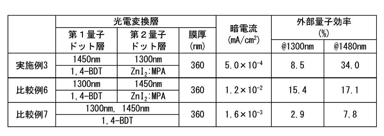
次に、実施例4ならびに比較例8について説明する。
以下の方法により光電変換素子を作製した。
それぞれの吸収ピーク波長が1300nmおよび1450nmである異なる粒子径を有するPbS量子ドットを質量比1:1で混合した20mg/mLオクタン溶液を用いて第1量子ドット層を形成し、それぞれの吸収ピーク波長が1000nmおよび1200nmである異なる粒子径を有するPbS量子ドットを質量比1:1で混合した20mg/mLオクタン溶液を用いて第2量子ドット層を形成したこと以外は、実施例2の場合と同様の方法で光電変換素子を形成した。作製した光電変換素子の光電変換層に用いられた量子ドットの吸収ピーク波長および表面修飾配位子ならびに光電変換層の膜厚を表4に示す。
それぞれの吸収ピーク波長が1000nm、1200nm、1300nmおよび1450nmである異なる粒子径を有するPbS量子ドットを質量比1:1:1:1で混合した20mg/mLオクタン溶液を用いた以外は、比較例5と同様の方法で光電変換素子を作製した。作製した光電変換素子の光電変換層に用いられた量子ドットの吸収ピーク波長および表面修飾配位子ならびに光電変換層の膜厚を表4に示す。
上記で作製した光電変換素子の評価として、上述の方法で暗電流および外部量子効率の測定を行った。暗電流の値、および、波長1000nm、1200nm、1360nmおよび1440nmでの外部量子効率の測定結果を表4に示す。

次に、実施例5ならびに比較例9について説明する。
以下の方法により光電変換素子を作製した。
酸化亜鉛を成膜する代わりに正孔ブロッキング層を真空蒸着によってフラーレン(C60)50nmの膜厚で形成したこと、および、正孔ブロッキング層上に、アルミニウム電極を形成する代わりにITOをスパッタ成膜により30nmの膜厚で成膜することでITO電極を形成したこと以外は、実施例4の場合と同様の方法で光電変換素子を形成した。作製した光電変換素子の光電変換層に用いられた量子ドットの吸収ピーク波長および表面修飾配位子ならびに光電変換層の膜厚を表5に示す。
酸化亜鉛を成膜する代わりに正孔ブロッキング層を真空蒸着によってフラーレン(C60)50nmの膜厚で形成したこと、および、正孔ブロッキング層上に、アルミニウム電極を形成する代わりにITOをスパッタ成膜により30nmの膜厚で成膜することでITO電極を形成したこと以外は、比較例8の場合と同様の方法で光電変換素子を形成した。作製した光電変換素子の光電変換層に用いられた量子ドットの吸収ピーク波長および表面修飾配位子ならびに光電変換層の膜厚を表5に示す。
上記で作製した光電変換素子の評価として、上述の方法で暗電流および外部量子効率の測定を行った。ただし、暗電流および外部量子効率は基板側のITO電極に-5Vの電圧を印加する条件にて測定した。また外部量子効率の測定時はITO基板側とは反対側のスパッタ成膜したITO電極側から光を入射して測定した。暗電流の値、および、波長1000nm、1180nm、1340nmおよび1480nmでの外部量子効率の測定結果を表5に示す。
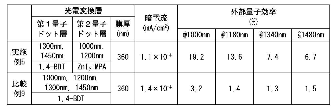
2 第1電極
3 第2電極
4 光電変換層
4a、4c 第1量子ドット層
4b、4d 第2量子ドット層
5 電子ブロッキング層
6 正孔ブロッキング層
10A、10B、10E 光電変換素子
10C、10D 光電変換部
20、20A 画素
22 蓄積制御線
23 電源線
24 垂直信号線
25 アドレス信号線
26 リセット信号線
27 フィードバック線
30 電圧供給回路
40 信号検出回路
41 電荷蓄積ノード
42 増幅トランジスタ
42e、44e、46e ゲート電極
42g、44g、46g ゲート絶縁層
44 アドレストランジスタ
46 リセットトランジスタ
52 垂直走査回路
54 水平信号読出し回路
56 カラム信号処理回路
58 負荷回路
59 反転増幅器
62 半導体基板
62a、62b、62c、62d、62e 不純物領域
62s 素子分離領域
63A、63B、63C 層間絶縁層
65A、65B コンタクトプラグ
66A 配線
67A、67B、67C プラグ
68A、68B 配線
72 保護層
74 マイクロレンズ
100、100A 撮像装置
Claims (11)
- 光電変換層と、
前記光電変換層で発生する正孔を捕集する第1電極と、
前記光電変換層を挟んで前記第1電極と対向し、前記光電変換層で発生する電子を捕集する第2電極と、を備え、
前記光電変換層は、
第1配位子で表面が修飾された複数の第1量子ドットを含む第1量子ドット層と、
前記第1量子ドット層と前記第2電極との間に位置し、前記第1配位子とは異なる第2配位子で表面が修飾された複数の第2量子ドットを含む第2量子ドット層と、を含み、
前記第2量子ドット層のイオン化ポテンシャルは、前記第1量子ドット層のイオン化ポテンシャルよりも大きく、
前記複数の第2量子ドットの粒子径分布を示す第2の値は、前記複数の第1量子ドットの粒子径分布を示す第1の値よりも小さい
光電変換素子。 - 前記複数の第1量子ドットおよび前記複数の第2量子ドットは、それぞれ、独立して、CdSe、CdS、PbS、PbSe、PbTe、ZnO、ZnS、Cu2ZnSnS4、Cu2S、CuInSe2、AgInS2、AgInTe2、CdSnAs2、ZnSnAs2、ZnSnSb2、Bi2S3、Ag2S、Ag2Te、HgTe、CdHgTe、Ge、GeSn、InAsおよびInSbのうちの少なくとも1つを含む、
請求項1に記載の光電変換素子。 - 前記第1配位子は、第1双極子モーメントを有し、
前記第2配位子は、第2双極子モーメントを有し、
前記第1双極子モーメントが前記複数の第1量子ドットの各々の外側に向く場合に前記第1双極子モーメントが正であり、前記第2双極子モーメントが前記複数の第2量子ドットの各々の外側に向く場合に前記第2双極子モーメントが正であるとすると、
前記第1双極子モーメントは、前記第2双極子モーメントより大きい、
請求項1または2に記載の光電変換素子。 - 前記第1配位子は1,4-ベンゼンジチオールであり、
前記第2配位子はZnI2と3-メルカプトプロピオン酸との混合物である、
請求項1から3のいずれか1項に記載の光電変換素子。 - 前記複数の第1量子ドットの粒子径分布、および、前記複数の第2量子ドットの粒子径分布の少なくとも一方は、異なる2つ以上の極大値を有する、
請求項1から4のいずれか1項に記載の光電変換素子。 - 複数の画素を備え、
前記複数の画素は、それぞれ、請求項1から5のいずれか1項に記載の光電変換素子を含む、
撮像装置。 - 前記第1電極に接続される信号読出し回路と、
前記第2電極の電位が前記第1電極の電位に対して正となる電圧を前記第2電極に供給する電圧供給回路と、をさらに備える、
請求項6に記載の撮像装置。 - 前記第2電極に接続される信号読み出し回路と、
前記第1電極の電位が前記第2電極の電位に対して負となる電圧を前記第1電極に供給する電圧供給回路と、をさらに備える、
請求項6に記載の撮像装置。 - 光電変換層と、
前記光電変換層で発生する正孔を捕集する第1電極と、
前記光電変換層を挟んで前記第1電極と対向し、前記光電変換層で発生する電子を捕集する第2電極と、を備え、
前記光電変換層は、
第1配位子で表面が修飾された複数の第1量子ドットを含む第1量子ドット層と、
前記第1量子ドット層と前記第2電極との間に位置し、前記第1配位子とは異なる第2配位子で表面が修飾された複数の第2量子ドットを含む第2量子ドット層と、を含み、
前記第2量子ドット層のイオン化ポテンシャルは、前記第1量子ドット層のイオン化ポテンシャルよりも大きく、
前記複数の第2量子ドットの吸収ピーク波長は、前記複数の第1量子ドットの吸収ピーク波長よりも小さく、
前記第1量子ドットの材料は、前記第2量子ドットの材料と異なる、
光電変換素子。 - 前記複数の第1量子ドットの粒子径分布を示す第2の値は、前記複数の第2量子ドットの粒子径分布を示す第1の値と等しい、
請求項9に記載の光電変換素子。 - 前記複数の第2量子ドットの粒子径分布を示す第2の値は、前記複数の第1量子ドットの粒子径分布を示す第1の値よりも大きい、
請求項9に記載の光電変換素子。
Priority Applications (4)
| Application Number | Priority Date | Filing Date | Title |
|---|---|---|---|
| JP2023522339A JPWO2022244575A1 (ja) | 2021-05-21 | 2022-04-19 | |
| CN202280035010.1A CN117321781A (zh) | 2021-05-21 | 2022-04-19 | 光电转换元件和摄像装置 |
| EP22804489.7A EP4343858A4 (en) | 2021-05-21 | 2022-04-19 | PHOTOELECTRIC CONVERSION ELEMENT AND IMAGING DEVICE |
| US18/490,823 US20240049490A1 (en) | 2021-05-21 | 2023-10-20 | Photoelectric conversion element and imaging device |
Applications Claiming Priority (2)
| Application Number | Priority Date | Filing Date | Title |
|---|---|---|---|
| JP2021-086045 | 2021-05-21 | ||
| JP2021086045 | 2021-05-21 |
Related Child Applications (1)
| Application Number | Title | Priority Date | Filing Date |
|---|---|---|---|
| US18/490,823 Continuation US20240049490A1 (en) | 2021-05-21 | 2023-10-20 | Photoelectric conversion element and imaging device |
Publications (1)
| Publication Number | Publication Date |
|---|---|
| WO2022244575A1 true WO2022244575A1 (ja) | 2022-11-24 |
Family
ID=84141353
Family Applications (1)
| Application Number | Title | Priority Date | Filing Date |
|---|---|---|---|
| PCT/JP2022/018142 Ceased WO2022244575A1 (ja) | 2021-05-21 | 2022-04-19 | 光電変換素子および撮像装置 |
Country Status (5)
| Country | Link |
|---|---|
| US (1) | US20240049490A1 (ja) |
| EP (1) | EP4343858A4 (ja) |
| JP (1) | JPWO2022244575A1 (ja) |
| CN (1) | CN117321781A (ja) |
| WO (1) | WO2022244575A1 (ja) |
Cited By (6)
| Publication number | Priority date | Publication date | Assignee | Title |
|---|---|---|---|---|
| WO2024176882A1 (ja) * | 2023-02-22 | 2024-08-29 | 富士フイルム株式会社 | 光検出素子およびイメージセンサ |
| WO2024176881A1 (ja) * | 2023-02-22 | 2024-08-29 | 富士フイルム株式会社 | 半導体膜、光検出素子、イメージセンサ、分散液および半導体膜の製造方法 |
| WO2025009817A1 (ko) * | 2023-07-06 | 2025-01-09 | 삼성디스플레이 주식회사 | 양자점 복합체, 양자점 복합체를 포함하는 발광 소자, 및 양자점 복합체를 포함하는 표시 장치 |
| WO2025047466A1 (ja) * | 2023-08-30 | 2025-03-06 | 富士フイルム株式会社 | 半導体膜、光検出素子およびイメージセンサ |
| WO2025072548A3 (en) * | 2023-09-29 | 2025-05-01 | Adeia Semiconductor Bonding Technologies Inc. | Stacked quantum dot sensors and methods of forming the same |
| WO2025120799A1 (ja) * | 2023-12-07 | 2025-06-12 | ソニーセミコンダクタソリューションズ株式会社 | 光検出装置および電子機器 |
Families Citing this family (1)
| Publication number | Priority date | Publication date | Assignee | Title |
|---|---|---|---|---|
| US20240081086A1 (en) * | 2020-12-22 | 2024-03-07 | Sharp Kabushiki Kaisha | Ligh-emitting element and light-emitting device |
Citations (7)
| Publication number | Priority date | Publication date | Assignee | Title |
|---|---|---|---|---|
| WO2015076300A1 (ja) * | 2013-11-19 | 2015-05-28 | 京セラ株式会社 | 光電変換層および光電変換装置 |
| US20150295107A1 (en) * | 2011-08-28 | 2015-10-15 | Edward Hartley Sargent | Quantum dot photo-field-effect transistor |
| JP2016162886A (ja) * | 2015-03-02 | 2016-09-05 | 京セラ株式会社 | 光電変換装置 |
| WO2017006520A1 (ja) * | 2015-07-08 | 2017-01-12 | パナソニックIpマネジメント株式会社 | 撮像装置 |
| JP6083813B2 (ja) | 2011-02-28 | 2017-02-22 | ユニバーシティ オブ フロリダ リサーチ ファウンデーション, インク.University Of Florida Reseatch Foundation, Inc. | 広帯域吸収体を有するアップコンバージョンデバイス |
| WO2017038698A1 (ja) * | 2015-08-28 | 2017-03-09 | 京セラ株式会社 | 光電変換装置 |
| JP2021064663A (ja) * | 2019-10-11 | 2021-04-22 | キヤノン株式会社 | 光電変換素子 |
Family Cites Families (9)
| Publication number | Priority date | Publication date | Assignee | Title |
|---|---|---|---|---|
| WO2009142677A2 (en) * | 2008-03-24 | 2009-11-26 | The Board Of Trustees Of The Leland Stanford Junior University | Quantum dot solar cell with quantum dot bandgap gradients |
| KR20120133700A (ko) * | 2011-05-31 | 2012-12-11 | 엘지이노텍 주식회사 | 태양전지 및 이의 제조방법 |
| WO2015056750A1 (ja) * | 2013-10-17 | 2015-04-23 | 株式会社村田製作所 | ナノ粒子材料、及び発光デバイス |
| CA2948486A1 (en) * | 2014-05-09 | 2015-11-12 | Massachusetts Institute Of Technology | Energy level modification of nanocrystals through ligand exchange |
| WO2016017763A1 (ja) * | 2014-07-30 | 2016-02-04 | 京セラ株式会社 | 量子ドット太陽電池 |
| US10897023B2 (en) * | 2015-10-02 | 2021-01-19 | Toyota Motor Europe | All quantum dot based optoelectronic device |
| EP3544074B1 (en) * | 2018-03-19 | 2025-06-04 | Samsung Electronics Co., Ltd. | Electroluminescent device, and display device comprising thereof |
| JP7527774B2 (ja) * | 2019-03-11 | 2024-08-05 | キヤノン株式会社 | 量子ドット、それを有する光電変換素子、受光素子、光電変換装置、移動体、量子ドットの製造方法、光電変換素子の製造方法 |
| KR102718280B1 (ko) * | 2019-09-20 | 2024-10-15 | 삼성전자주식회사 | 전계 발광 소자 및 이를 포함하는 표시 장치 |
-
2022
- 2022-04-19 EP EP22804489.7A patent/EP4343858A4/en active Pending
- 2022-04-19 CN CN202280035010.1A patent/CN117321781A/zh active Pending
- 2022-04-19 JP JP2023522339A patent/JPWO2022244575A1/ja active Pending
- 2022-04-19 WO PCT/JP2022/018142 patent/WO2022244575A1/ja not_active Ceased
-
2023
- 2023-10-20 US US18/490,823 patent/US20240049490A1/en active Pending
Patent Citations (9)
| Publication number | Priority date | Publication date | Assignee | Title |
|---|---|---|---|---|
| JP6083813B2 (ja) | 2011-02-28 | 2017-02-22 | ユニバーシティ オブ フロリダ リサーチ ファウンデーション, インク.University Of Florida Reseatch Foundation, Inc. | 広帯域吸収体を有するアップコンバージョンデバイス |
| US20150295107A1 (en) * | 2011-08-28 | 2015-10-15 | Edward Hartley Sargent | Quantum dot photo-field-effect transistor |
| WO2015076300A1 (ja) * | 2013-11-19 | 2015-05-28 | 京セラ株式会社 | 光電変換層および光電変換装置 |
| JP6255417B2 (ja) | 2013-11-19 | 2017-12-27 | 京セラ株式会社 | 光電変換装置 |
| JP2016162886A (ja) * | 2015-03-02 | 2016-09-05 | 京セラ株式会社 | 光電変換装置 |
| WO2017006520A1 (ja) * | 2015-07-08 | 2017-01-12 | パナソニックIpマネジメント株式会社 | 撮像装置 |
| WO2017038698A1 (ja) * | 2015-08-28 | 2017-03-09 | 京セラ株式会社 | 光電変換装置 |
| JP6298223B2 (ja) | 2015-08-28 | 2018-03-20 | 京セラ株式会社 | 光電変換装置 |
| JP2021064663A (ja) * | 2019-10-11 | 2021-04-22 | キヤノン株式会社 | 光電変換素子 |
Non-Patent Citations (2)
| Title |
|---|
| PRADHAN SANTANU, STAVRINADIS ALEXANDROS, GUPTA SHUCHI, BI YU, DI STASIO FRANCESCO, KONSTANTATOS GERASIMOS: "Trap-State Suppression and Improved Charge Transport in PbS Quantum Dot Solar Cells with Synergistic Mixed-Ligand Treatments", SMALL, WILEY, vol. 13, no. 21, 1 June 2017 (2017-06-01), pages 1 - 9, XP055782946, ISSN: 1613-6810, DOI: 10.1002/smll.201700598 * |
| See also references of EP4343858A4 |
Cited By (6)
| Publication number | Priority date | Publication date | Assignee | Title |
|---|---|---|---|---|
| WO2024176882A1 (ja) * | 2023-02-22 | 2024-08-29 | 富士フイルム株式会社 | 光検出素子およびイメージセンサ |
| WO2024176881A1 (ja) * | 2023-02-22 | 2024-08-29 | 富士フイルム株式会社 | 半導体膜、光検出素子、イメージセンサ、分散液および半導体膜の製造方法 |
| WO2025009817A1 (ko) * | 2023-07-06 | 2025-01-09 | 삼성디스플레이 주식회사 | 양자점 복합체, 양자점 복합체를 포함하는 발광 소자, 및 양자점 복합체를 포함하는 표시 장치 |
| WO2025047466A1 (ja) * | 2023-08-30 | 2025-03-06 | 富士フイルム株式会社 | 半導体膜、光検出素子およびイメージセンサ |
| WO2025072548A3 (en) * | 2023-09-29 | 2025-05-01 | Adeia Semiconductor Bonding Technologies Inc. | Stacked quantum dot sensors and methods of forming the same |
| WO2025120799A1 (ja) * | 2023-12-07 | 2025-06-12 | ソニーセミコンダクタソリューションズ株式会社 | 光検出装置および電子機器 |
Also Published As
| Publication number | Publication date |
|---|---|
| EP4343858A1 (en) | 2024-03-27 |
| CN117321781A (zh) | 2023-12-29 |
| US20240049490A1 (en) | 2024-02-08 |
| JPWO2022244575A1 (ja) | 2022-11-24 |
| EP4343858A4 (en) | 2024-11-13 |
Similar Documents
| Publication | Publication Date | Title |
|---|---|---|
| WO2022244575A1 (ja) | 光電変換素子および撮像装置 | |
| Xu et al. | Photodetectors based on solution-processable semiconductors: Recent advances and perspectives | |
| Ghosh et al. | Recent advances in perovskite/2D materials based hybrid photodetectors | |
| US8742398B2 (en) | Quantum dot-fullerene junction based photodetectors | |
| US9349970B2 (en) | Quantum dot-fullerene junction based photodetectors | |
| US9054262B2 (en) | Integrated optical upconversion devices and related methods | |
| JP7535701B2 (ja) | 撮像装置 | |
| CN104956483A (zh) | 使用溶液处理pbs光探测器的新型ir图像传感器 | |
| KR20150102962A (ko) | 중간 밴드 반도체들, 이종접합들, 및 용액 처리된 양자 점들을 이용한 광전자 소자들, 및 관련 방법들 | |
| US20240381677A1 (en) | Photoelectric conversion element and imaging apparatus | |
| So et al. | Advancements and Challenges of Vacuum‐Processed Organic Photodiodes: A Comprehensive Review | |
| JP7713649B2 (ja) | 撮像装置および駆動方法 | |
| US12101949B2 (en) | Photoelectric conversion element, electronic device, and light-emitting device | |
| US20240365657A1 (en) | Photoelectric conversion element, imaging device, and fullerene derivative solution | |
| US11777050B2 (en) | Optical sensor | |
| JP7620852B2 (ja) | 撮像装置 | |
| WO2021149414A1 (ja) | 撮像装置 | |
| US20240065013A1 (en) | Photoelectric conversion element, imaging apparatus, and method for driving photoelectric conversion element | |
| JP2021174900A (ja) | 撮像装置 | |
| US20250393385A1 (en) | Photoelectric conversion element and imaging device | |
| JP2026032297A (ja) | 光電変換素子および撮像装置 | |
| CN121398179A (zh) | 一种感光像素单元以及图像传感器 | |
| WO2024214448A1 (ja) | 光電変換素子および撮像装置 | |
| CN121619982A (zh) | 一种含有p型薄膜晶体管传输门的感光像素元件及图像传感器 | |
| WO2022149401A1 (ja) | 撮像装置 |
Legal Events
| Date | Code | Title | Description |
|---|---|---|---|
| 121 | Ep: the epo has been informed by wipo that ep was designated in this application |
Ref document number: 22804489 Country of ref document: EP Kind code of ref document: A1 |
|
| WWE | Wipo information: entry into national phase |
Ref document number: 2023522339 Country of ref document: JP |
|
| WWE | Wipo information: entry into national phase |
Ref document number: 202280035010.1 Country of ref document: CN |
|
| WWE | Wipo information: entry into national phase |
Ref document number: 2022804489 Country of ref document: EP |
|
| NENP | Non-entry into the national phase |
Ref country code: DE |
|
| ENP | Entry into the national phase |
Ref document number: 2022804489 Country of ref document: EP Effective date: 20231221 |