WO2022244730A1 - ワイヤレス給電システム及び方法並びにワイヤレス送電システム - Google Patents
ワイヤレス給電システム及び方法並びにワイヤレス送電システム Download PDFInfo
- Publication number
- WO2022244730A1 WO2022244730A1 PCT/JP2022/020380 JP2022020380W WO2022244730A1 WO 2022244730 A1 WO2022244730 A1 WO 2022244730A1 JP 2022020380 W JP2022020380 W JP 2022020380W WO 2022244730 A1 WO2022244730 A1 WO 2022244730A1
- Authority
- WO
- WIPO (PCT)
- Prior art keywords
- coil
- power
- power supply
- impedance
- load
- Prior art date
- Legal status (The legal status is an assumption and is not a legal conclusion. Google has not performed a legal analysis and makes no representation as to the accuracy of the status listed.)
- Ceased
Links
Images


Classifications
-
- H—ELECTRICITY
- H02—GENERATION; CONVERSION OR DISTRIBUTION OF ELECTRIC POWER
- H02J—ELECTRIC POWER NETWORKS; CIRCUIT ARRANGEMENTS OR SYSTEMS FOR SUPPLYING OR DISTRIBUTING ELECTRIC POWER; SYSTEMS FOR STORING ELECTRIC ENERGY
- H02J50/00—Circuit arrangements or systems for wireless supply or distribution of electric power
- H02J50/10—Circuit arrangements or systems for wireless supply or distribution of electric power using inductive coupling
- H02J50/12—Circuit arrangements or systems for wireless supply or distribution of electric power using inductive coupling of the resonant type
-
- H—ELECTRICITY
- H02—GENERATION; CONVERSION OR DISTRIBUTION OF ELECTRIC POWER
- H02J—ELECTRIC POWER NETWORKS; CIRCUIT ARRANGEMENTS OR SYSTEMS FOR SUPPLYING OR DISTRIBUTING ELECTRIC POWER; SYSTEMS FOR STORING ELECTRIC ENERGY
- H02J50/00—Circuit arrangements or systems for wireless supply or distribution of electric power
- H02J50/40—Circuit arrangements or systems for wireless supply or distribution of electric power using two or more transmitting or receiving devices
-
- H—ELECTRICITY
- H02—GENERATION; CONVERSION OR DISTRIBUTION OF ELECTRIC POWER
- H02J—ELECTRIC POWER NETWORKS; CIRCUIT ARRANGEMENTS OR SYSTEMS FOR SUPPLYING OR DISTRIBUTING ELECTRIC POWER; SYSTEMS FOR STORING ELECTRIC ENERGY
- H02J50/00—Circuit arrangements or systems for wireless supply or distribution of electric power
- H02J50/50—Circuit arrangements or systems for wireless supply or distribution of electric power using additional energy repeaters between transmitting devices and receiving devices
-
- H—ELECTRICITY
- H02—GENERATION; CONVERSION OR DISTRIBUTION OF ELECTRIC POWER
- H02J—ELECTRIC POWER NETWORKS; CIRCUIT ARRANGEMENTS OR SYSTEMS FOR SUPPLYING OR DISTRIBUTING ELECTRIC POWER; SYSTEMS FOR STORING ELECTRIC ENERGY
- H02J50/00—Circuit arrangements or systems for wireless supply or distribution of electric power
- H02J50/80—Circuit arrangements or systems for wireless supply or distribution of electric power involving the exchange of data, concerning supply or distribution of electric power, between transmitting devices and receiving devices
-
- H—ELECTRICITY
- H03—ELECTRONIC CIRCUITRY
- H03H—IMPEDANCE NETWORKS, e.g. RESONANT CIRCUITS; RESONATORS
- H03H7/00—Multiple-port networks comprising only passive electrical elements as network components
- H03H7/38—Impedance-matching networks
Definitions
- the present invention relates to a wireless power supply system and method, and a wireless power supply system.
- An electromagnetic coupling (electromagnetic induction) method and a magnetic resonance method are known as power feeding methods using such magnetism.
- the magnetic field resonance method the oscillation of the magnetic field generated by the alternating current flowing through the resonance circuit of the power transmission device is transmitted to the resonance circuit of the power reception device and resonates, so that the magnetic field generated by the coil of each resonance circuit becomes strong.
- Wireless power supply using the magnetic resonance method has the advantage that the distance over which power can be supplied is longer than wireless power supply using the electromagnetic coupling method (see Patent Document 1, for example).
- the magnetic resonance method is also a method using magnetic coupling, the method using resonance is referred to as the magnetic resonance method in the present invention in order to facilitate understanding.
- the impedance of the load side circuit including the power receiving device and the load, etc. viewed from the power transmitting device and the impedance of the power source side viewed from the power transmitting device are set to be equivalent. There is a need.
- a wireless power supply system is a wireless power supply system that transmits and receives power using magnetism, comprising: a power transmission side resonance circuit including a power transmission coil; and a magnetic field coupling with the power transmission coil.
- a wireless power supply method includes: a power transmission side resonance circuit including a power transmission coil; a power feeding coil that transmits power to a coil; and a power receiving device that includes a power receiving side resonance circuit including a power receiving coil and supplies power received by the power receiving coil to a load, and uses magnetism.
- the difference between the load-side impedance, which is the impedance of the circuit on the load side from the input end of the power transmission device, and the input-side impedance, which is the impedance of the circuit on the power supply device side from the input end of the power transmission device, is reduced.
- the present invention even if the impedance of the load-side circuit fluctuates, the difference between the input-side impedance and the load-side impedance is reduced. , the risk of system failure associated therewith can be avoided.
- FIG. 1 is a schematic diagram showing the configuration of a wireless power supply system according to a first embodiment of the present invention
- FIG. FIG. 3 is a schematic diagram showing the configuration of an impedance matching mechanism
- 1 is a circuit diagram corresponding to a wireless power supply system
- FIG. 4 is an equivalent circuit diagram corresponding to the circuit diagram shown in FIG. 3
- FIG. 4 is a graph showing the relationship between load voltage and load current
- 4 is a graph showing the relationship between load current and load-side impedance
- FIG. 4 is a schematic diagram showing the positional relationship between a power transmission coil and three power supply coil units arranged to be offset in the axial direction of the coil axis
- 7 is a graph showing the relationship between the distance from the power supply coil to the power transmission coil and the load resistance
- FIG. 4 is a schematic diagram showing how the coil moving mechanism slides the feeding coil in the direction perpendicular to the coil axis.
- FIG. 4 is a schematic diagram showing how the coil moving mechanism slides the feeding coil parallel to the coil axis.
- FIG. 3 is a schematic diagram showing the positional relationship between a power transmission coil and three power supply coil units that are arranged to be offset in the vertical direction with respect to the axial direction of the coil axis;
- FIG. 4 is a schematic diagram showing a positional relationship between a power transmission coil and eight power supply coil units that are arranged in a substantially spherical shape with an inclination with respect to the power transmission coil. It is a schematic diagram which shows the positional relationship with the power transmission coil and the three feed coil parts which comprise the feed coil formed spirally.
- FIG. 5 is a schematic diagram showing the configuration of an impedance matching mechanism applied to a wireless power supply system according to a second embodiment of the present invention
- FIG. 11 is a schematic diagram showing how a coil moving mechanism applied to a wireless power feeding system according to a third embodiment of the present invention moves a power feeding coil in a direction perpendicular to a coil axis
- FIG. 11 is a schematic diagram showing how a coil moving mechanism applied to a wireless power supply system according to a third embodiment of the present invention swings a power supply coil;
- drawings may exaggerate by enlarging and exaggerating characteristic parts in order to make the features easier to understand, and the dimensional ratios, etc. of the constituent elements may not necessarily be the same as the actual ones.
- hatching of some components may be omitted in order to facilitate understanding of the cross-sectional structure of the components.
- FIG. 1 is a schematic diagram showing the configuration of a wireless power supply system 1.
- the wireless power supply system 1 uses magnetic field resonance to contactlessly supply electric power to a power supply target 2 .
- the power supply object 2 is, for example, a vehicle, a flying robot, an underwater robot, a capsule endoscope, a cardiac pacemaker, or the like, and may be either a movable device or an immovable device. In addition, the power supply object 2 may be moving or stopped at the time of power supply.
- a wireless power supply system 1 includes a power transmission device 3 and a power reception device 4 .
- the power transmitting device 3 includes a power feeding coil 31 , a power transmitting coil 32 , and capacitors 33 and 34 .
- the power feeding coil 31 and the power transmitting coil 32 are formed by winding a copper wire or the like with high electrical conductivity in a circular shape. It should be noted that the current flowing through the copper wire flows more in the vicinity of the surface of the copper wire than in the central portion due to the influence of internal resistance. Therefore, when a litz wire obtained by twisting a plurality of copper wires is used as the wire material of the power supply coil 31 and the power transmission coil 32, the litz wire has a larger surface area than a single copper wire with the same diameter. A large amount of current can flow, and current loss can be suppressed.
- the AC power is supplied from the AC power supply 5 to the feeding coil 31 .
- the AC power is set to, for example, a frequency of 150 kHz and a voltage of 10 V, but the frequency and voltage of the AC power supply 5 can be changed arbitrarily.
- the contact of the feeding coil 31 on the AC power supply 5 side will be referred to as an "input terminal IE".
- the case where the feed coil 31 and the AC power supply 5 are directly connected via the input terminal IE will be described as an example.
- the connection may be made directly through the IE or indirectly through a coaxial cable or the like provided between the AC power supply 5 and the input terminal IE. In this case, if the impedance of the power source matches the impedance of the coaxial cable, etc., there is no problem because the power source side end of the coaxial cable, etc. does not reflect power, and the input end IE means the load end of
- the power supply coil 31 and the capacitor 33 are connected in series to form a power supply side resonance circuit 35 .
- an AC voltage having a frequency corresponding to the resonance frequency set by the inductance of the feeding coil 31 and the capacitance of the capacitor 33 flows through the feeding coil 31 , an oscillating magnetic field is generated to penetrate the feeding coil 31 .
- a detailed configuration of the feeding coil 31 will be described later.
- the power supply coil 31 and the power transmission coil 32 are magnetically coupled, and the power supply coil 31 supplies power to the power transmission coil 32 by a magnetic resonance method. That is, the resonance frequency set according to the inductance of the power supply coil 31 and the capacitance of the capacitor 33 is substantially equal to the resonance frequency set according to the inductance of the power transmission coil 32 and the capacitance of the capacitor 34, and the power supply coil 31 and power transmission It is designed to resonate with the coil 32 . As a result, the vibration of the magnetic field of a specific frequency (resonant frequency) generated by the flow of alternating current in the power feeding coil 31 is transmitted to the power transmitting coil 32 and resonates at the same specific frequency, thereby generating an electromotive force in the power transmitting coil 32 .
- a specific frequency resonant frequency
- the power transmission coil 32 and the capacitor 34 are connected in series to form a power transmission side resonance circuit 36 .
- the power reception coil 41 which will be described later, resonates to generate an electromotive force.
- the power receiving device 4 is provided inside the power supply object 2 .
- the power receiving device 4 includes a power receiving coil 41 and a capacitor 42 .
- the feeding coil 31 is divided into three feeding coil portions 31A, 31B, and 31C.
- the three feeding coil portions 31A, 31B, and 31C divide the feeding coil 31 into three and are substantially connected in series, and the feeding coil portions 31A and 31B are connected via wiring 31AB, The feed coil portions 31B and 31C are connected via a wiring 31BC. Note that the wirings 31AB and 31BC may be omitted if necessary.
- the coil axes 31a, 31b, and 31c of the power feeding coil portions 31A, 31B, and 31C and the coil axis 32a of the power transmitting coil 32 are positioned substantially coaxially in the normal state. In the following description, an example in which the feeding coil 31 is divided into three feeding coil sections 31A, 31B, and 31C will be described. do not have.
- the switches 91a to 91d are three-way switches for supplying current to the feed coil portions 31A, 31B, and 31C.
- the switches 91 a and 91 b are connected to the AC power supply 5 .
- the switch 91a is configured to be switchable between one end side of the feeding coil portion 31C and the switch 91c side.
- the switch 91c is configured to be able to switch between one end side of the feeding coil portion 31A and one end side of the feeding coil portion 31B.
- the switch 91b is configured to be able to switch between the other end side of the feeding coil portion 31C and the switch 91d side.
- the switch 91d is configured to be able to switch between the other end side of the feeding coil portion 31A and the other end side of the feeding coil portion 31B.
- the switch 91a When power is supplied to the feed coil section 31A, the switch 91a is switched to the switch 91c side, the switch 91c is switched to one end side of the feed coil section 31A, the switch 91b is switched to the switch 91d side, and the switch 91d is switched to the feed coil side. Switch to the other end side of the portion 31A.
- the switch 91a When power is supplied to the power supply coil section 31B, the switch 91a is switched to the switch 91c side, the switch 91c is switched to the one end side of the power supply coil section 31B, the switch 91b is switched to the switch 91d side, and the switch 91d is switched. Switch to the other end side of the feeding coil portion 31B.
- the switch 91a when power is supplied to the feeding coil section 31C, the switch 91a is switched to the feeding coil section 31C side, and the switch 91b is switched to the feeding coil section 31C side.
- the switch 91a When power is supplied to the feed coil units 31A and 31B, the switch 91a is switched to the switch 91c side, the switch 91c is switched to one end of the feed coil unit 31A, the switch 91b is switched to the switch 91d side, and the switch 91d is switched to the other end side of the feeding coil portion 31B.
- the switch 91a When power is supplied to the feed coil units 31B and 31C, the switch 91a is switched to the switch 91c side, the switch 91c is switched to one end of the feed coil unit 31B, and the switch 91b is switched to the feed coil unit 31C side.
- FIG. 3 is a circuit diagram corresponding to the wireless power supply system 1. As shown in FIG. In FIG. 3, “V” is the voltage of the power supply 5, “Z s ” is the impedance of the power supply 5 (input side impedance), “R 0 ” is the parasitic resistance of the feeding coil 31, and “L 0 ” is the inductance of the feeding coil 31.
- Z 1 is the impedance of the circuit on the load 8 side from between the power feeding coil 31 and the power transmitting coil 32 .
- Z 2 is the impedance of the circuit on the load 8 side from between the power feeding coil 31 and the power transmitting coil 32 . Equations 1 to 3 below are obtained from the equivalent circuit shown in FIG.
- the power transmission coil 32 and the power feeding coil units 31B and 31C can be controlled according to the distance between them.
- the magnetic field coupling becomes looser and the coupling coefficient k01 becomes smaller.
- the load side Impedance Z0 can be kept constant. In this way, by continuing to control the load-side impedance Z0 to be approximately equal to the input-side impedance Zs , power reflection is suppressed, and an efficient system driving situation can be realized.
- the storage unit 93 stores the relationship between the load voltage and the load current output from the DC-DC converter 7 and supplied to the load 8, and the relationship between the load current and the load impedance.
- the load voltage and load current supplied to the load 8 are continuously measured in real time by a measuring section 95 provided between the DC-DC converter 7 and the load 8 .
- the measurement unit 95 is not limited to one that measures the load voltage, and may be one that measures the load current, or both.
- the load voltage and load current in this embodiment are the output voltage and output current from the DC-DC converter 7 , in other words, the input voltage and input current of the load 8 .
- the measurement unit 95 can be arranged between the capacitor 62 and the DC-DC converter 7 . In this case, the load voltage and load current are the input voltage and input current of the DC-DC converter 7 . Furthermore, when the DC-DC converter 7 is not arranged, the load voltage and load current are the input voltage and input current of the load 8 .
- the relationship between the load current and the load impedance is the relationship between the load current and the load impedance when the DC-DC converter 7 is idling (converter OFF). It includes the relationship between the load current and the load-side impedance when the converter 7 is not operating (converter ON).
- the output voltage of the DC-DC converter 7 is, for example, 12 V or less, which is the operating voltage, and the load current is very small.
- the load current (output current of the DC-DC converter 7) when the measurement unit 95 is arranged between the DC-DC converter 7 and the load 8 is almost zero, and the measurement unit 95 is placed between the capacitor 62 and the DC-DC converter. 7, the load current (input current of the DC-DC converter 7) increases slightly until it reaches the operating voltage (eg 12V). Then, the load-side impedance at this time becomes extremely large as shown in FIG.
- the load-side impedance becomes a substantially constant value (a value equivalent to the power of the load intended for the device).
- the measuring section 95 is arranged between the capacitor 62 and the DC-DC converter 7, the load-side impedance slightly decreases.
- the load-side impedance at this time sharply decreases and asymptotically approaches a predetermined value with the lapse of time. This is the same when the measuring section 95 is arranged between the capacitor 62 and the DC-DC converter 7.
- the value of the load-side impedance is adjusted in advance in the idling state before the DC-DC converter 7 starts operating. do.
- the input-side impedance is fixed at a predetermined value (for example, 50 ⁇ ). Impedance does not match, and a reflected wave is generated at the input terminal IE, which may reduce power transmission efficiency, or cause system failure due to insufficient power transmission.
- control unit 94 calculates the load current based on the load voltage measured by the measurement unit 95 and FIG. Also, the control unit 94 calculates the load-side impedance based on the calculated load current and FIG.
- the relationship between the distance between the power feeding coil units 31A, 31B, and 31C and the power transmitting coil 32 and the amount of change in the coupling coefficient is obtained in advance through experiments or the like.
- the wireless power supply system 1 is a wireless power supply system 1 that transmits and receives power using magnetism, and includes the power transmission side resonance circuit 36 including the power transmission coil 32 and the power transmission coil 32.
- a power transmission device 3 including a power transmission coil 31 which is provided so as to be magnetically coupled and which transmits power supplied from an input terminal IE to the power transmission coil 32;
- the impedance matching mechanism 9 changes the strength of the magnetic field coupling between the power supply coil 31 and the power transmission coil 32 (magnetic field coupling density).
- the difference between the input side impedance and the load side impedance is reduced, so the generation of reflected waves at the input terminal IE is suppressed, and system failure due to a decrease in power transmission efficiency and a decrease in power transmission can be avoided. can.
- the plurality of power supply coil units 31A, 31B, and 31C are provided with coil axes 31a, 31b, and 31c arranged substantially coaxially with each other, and the distance from the power transmission coil 32 is are set differently.
- the strength of the magnetic field coupling between the power feeding coil units 31A, 31B, and 31C and the power transmitting coil 32 weakens in inverse proportion to the distance of the power feeding coil units 31A, 31B, and 31C from the power transmitting coil 32.
- power is supplied from the power supply coil 31 to the power transmission coil 32 by a magnetic resonance method, and the inductance values of the power supply coil sections 31A, 31B, and 31C are substantially equal. Configured as set.
- the wireless power supply system 1 further includes a measuring unit 95 that measures the load current supplied to the load 8 or the load voltage applied to the load 8, and the impedance matching mechanism 9
- the configuration is such that impedance matching processing is performed according to the measurement results.
- the impedance matching mechanism 9 reduces the difference between the input side impedance and the load side impedance according to the measurement result of the measuring unit 95, so that the generation of the reflected wave at the input terminal IE is suppressed, and the power transmission efficiency is improved. It is possible to avoid system failures caused by drops and reductions in transmitted power.
- the wireless power supply system 1 is configured such that power is supplied from the power transmission coil 32 to the power reception coil 41 by a magnetic resonance method.
- the wireless power supply method using the wireless power supply system 1 includes a power transmission side resonance circuit 36 including the power transmission coil 32, a power transmission side resonance circuit 36 provided so as to be magnetically coupled with the power transmission coil 32, and power supplied from the input terminal IE. to the power transmitting coil 32, and the power receiving device 4, which includes a power receiving side resonance circuit 43 including the power receiving coil 41 and supplies the power received by the power receiving coil 41 to the load 8.
- a wireless power supply method using a wireless power supply system 1 that transmits and receives power using magnetism, and uses an impedance matching mechanism 9 to perform magnetic field coupling between the power supply coil 31 and the power transmission coil 32.
- the load-side impedance which is the impedance of the circuit from the input terminal IE of the power transmission device 3 to the load 8 side
- the input-side impedance which is the impedance of the circuit from the input terminal IE of the power transmission device 3 to the AC power supply 5 side
- the impedance matching mechanism 9 changes the strength of the magnetic field coupling between the power supply coil 31 and the power transmission coil 32, so that the input-side impedance and the load-side impedance, the generation of reflected waves at the input end IE is suppressed, and system failures caused by reduced power transmission efficiency and reduced power transmission can be avoided.
- the wireless power transmission system 11 is a wireless power transmission system 11 that uses magnetism to transmit power to the power receiving device 4, and includes a power transmission side resonance circuit 36 including the power transmission coil 32, and the power transmission coil 32.
- a power transmission device 3 that is provided to be magnetically coupled and that transmits power supplied from an input terminal IE to a power transmission coil 32, and that transmits power to a load 8 via a power reception device 4; 31 and the power transmission coil 32, the load-side impedance, which is the impedance of the circuit on the load 8 side, from the input end IE of the power transmission device 3 and the AC power supply from the input end IE of the power transmission device 3 and an impedance matching mechanism 9 that performs an impedance matching process for reducing the difference from the input side impedance, which is the impedance of the circuit on the 5 side.
- the impedance matching mechanism 9 changes the strength of the magnetic field coupling between the power supply coil 31 and the power transmission coil 32, so that the input-side impedance and the load-side impedance, the generation of reflected waves at the input end IE is suppressed, and system failures caused by reduced power transmission efficiency and reduced power transmission can be avoided.
- the input side impedance and the load side impedance are matched in advance when the DC-DC converter 7 is idling.
- the input side impedance and the load side impedance may be matched in advance when the DC-DC converter 7 is turned on or when the load side impedance is stabilized after the DC-DC converter 7 is turned on.
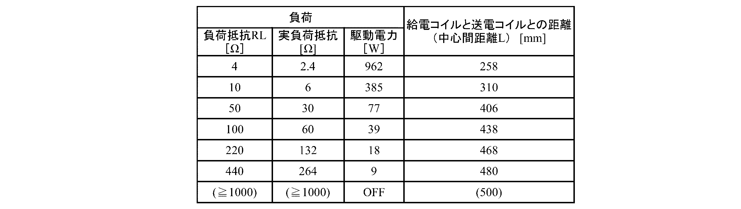
- the actual load resistance of the load 8 was calculated in consideration of the load resistance of the rectifier circuit 6 and the DC-DC converter 7 when the output voltage of the DC-DC converter 7 was 48V. Those results are shown in Table 1 and FIG. FIG. 8 is a graph in which the horizontal axis represents the load resistance RL, and the vertical axis represents the center-to-center distance L between the feeding coil 31 and the transmitting coil 32 when the impedances are matched.
- the load resistance RL is set to 1000 ⁇ or more (the actual load resistance of the load 8 is 1000 ⁇ or more) for convenience, and the center-to-center distance L at this time is set to 500 mm.
- the measuring portion 95 The load current is measured to calculate the drive power value of the load 8, and the feed coil units 31A, 31B, and 31C are switched by switching the switches 91a to 91d according to the calculated drive power of the load 8. Specifically, when the driving power of the load 8 is 200 W or more, the power feeding coil section 31B is set to the power feeding coil section 31C when the driving power of the load 8 is 20 W or more and less than 200 W. It is activated when it is OFF or the driving power of the load 8 is less than 20W.
- the number of power feeding coils 31 is increased to 6, and the installation positions of the power feeding coils 31 are set to 250 mm, 300 mm, 350 mm, 400 mm, 450 mm, and 500 mm in terms of center-to-center distance L from the power transmitting coil 32 .
- the power supply coil with the center distance L of 250 mm has a center distance of
- the feeding coil with L of 350 mm has a center-to-center distance L of 450 mm when the driving power of the load 8 is 200 W or more and less than 350 W.
- the feeding coils are operated when the driving power of the load 8 is 10 W or more and less than 50 W, and the feeding coil with the center-to-center distance L of 500 mm is operated when the load 8 is OFF or the driving power of the load 8 is less than 10 W.
- the plurality of power supply coils 31 do not necessarily have to be arranged at equal intervals, and the intervals between the power supply coils 31 may be changed as necessary.
- the number of feed coils 31 installed in a region where the drive power of the load 8 is small, where the drive power increases sharply when the load 8 is started, is changed to a region where the drive power of the load 8 is large and stable to some extent, and where the drive power is large. The number may be increased from 31.
- the installation positions of the power supply coils 31 are arranged at positions with a center-to-center distance L from the power supply coil 32 of 300 mm, 400 mm, 440 mm, 470 mm, 490 mm, and 500 mm.
- the feed coil 31 arranged with the center distance L of 300 mm has a drive power of 500 W or more for the load 8
- the feed coil 31 arranged with the center distance L of 400 mm has a drive power of the load 8 of 500 W or more.
- the power feeding coil 31 with the center distance L of 470 mm is 470 mm.
- the power feeding coil 31 with the center distance L of 500 mm is turned off or the load is turned off. 8 operate when the driving power is less than 5W.
- the impedance matching mechanism 9 may include a coil moving mechanism 96 that relatively moves the power feeding coil 31 with respect to the power transmitting coil 32, as shown in FIGS. 9(a) and 9(b).
- the coil moving mechanism 96 is a solenoid that includes a plunger 96a and a case 96b.
- a feeding coil 31 is connected to the tip of the plunger 96a.
- the plunger 96a advances and retracts in the direction perpendicular to the coil axes 31a, 31b, and 31c, thereby maintaining the coil axes 31a, 31b, and 31c and the coil axis 32a of the power transmission coil 32 in a substantially parallel state.
- the feeding coil 31 is slid so that the coil axes 31a, 31b, and 31c are relatively separated from or close to (coincident with) the coil axis 32a.
- the position of the power feeding coil 31 when the coil axes 31a, 31b, and 31c are coaxial with the coil axis 32a of the power transmitting coil 32 is set to the original position.
- the plunger 96a is retracted, and the feed coil 31 moves away from the original position in the direction perpendicular to the coil axes 31a, 31b, and 31c, and ), the plunger 96a advances, and the feeding coil 31 moves away from the original position in the direction orthogonal to the coil axes 31a, 31b, and 31c.
- the magnetic field coupling with the power transmission coil 32 becomes dense (coupling strength (coupling coefficient) increases. Become).
- the coil axes 31a, 31b, and 31c are offset with respect to the coil axis 32a of the power transmission coil 32 in the direction orthogonal to the coil axis 31a, the magnetic field coupling with the power transmission coil 32 becomes sparse (coupling strength (coupling coefficient) becomes smaller).
- the relationship between the amount of offset (the stroke amount of the plunger 96a) of the coil axis 31a of the power supply coil 31 and the coil axis 32a of the power transmission coil 32 and the amount of change in the impedance of the circuit in the power transmission device 3 is obtained in advance by experiment or the like.
- the stroke range (one side) of the plunger 96a is set to be equal to or less than the radius of the feeding coil 31, for example.
- the power feeding coil 31 is At least a portion can be kept in a state of overlapping with at least a portion of the power transmission coil 32 .
- a mechanism for moving the power feeding coil 31 relative to the power transmitting coil 32 by such a coil moving mechanism 96 is inferior in responsiveness compared to a configuration in which the switches 91a to 91d are electrically switched.
- the impedance can be smoothly optimized by finely adjusting the impedance by moving the power feeding coil 31 relative to the power transmitting coil 32 .
- the impedance may be optimized by moving the power feeding coil 31 relative to the power transmitting coil 32 to roughly adjust the impedance, and then finely adjusting the impedance by switching control of the switches 91a to 91d. .
- Modification 2 In Modification 1 described above, the configuration in which the coil moving mechanism 96 moves the power feeding coil 31 so that the coil axis 31a of the power feeding coil 31 is offset in the direction orthogonal to the coil axis 32a of the power transmitting coil 32 was illustrated.
- the moving mechanism 96 may be configured to move the feeding coil 31 in parallel with the axial direction of the coil shafts 31a, 31b, 31c and the coil shaft 32a.
- the plunger 96a is retracted to move the power feeding coil 31 from the original position in a direction parallel to the coil axes 31a, 31b, and 31c and away from the power transmitting coil 32.
- the plunger 96a advances, and the coil moving mechanism 96 moves the feeding coil 31 from the original position in a direction parallel to the coil axes 31a, 31b, and 31c and closer to the transmitting coil 32.
- the relationship between the amount by which the coil moving mechanism 96 moves the feeding coil 31 (the stroke amount of the plunger 96a) and the amount of change in the impedance of the circuit in the power transmission device 3 is obtained in advance through experiments or the like.
- a mechanism for moving the power feeding coil 31 relative to the power transmitting coil 32 by such a coil moving mechanism 96 is inferior in responsiveness compared to a configuration in which the switches 91a to 91d are electrically switched. After roughly adjusting the impedance by switching control, the power supply coil 31 is relatively moved with respect to the power transmission coil 32 to finely adjust the impedance, thereby smoothly optimizing even when the impedance value changes greatly. be able to.
- the power feeding coil portion 31A is arranged at a position with a center-to-center distance L of 300 mm from the power transmission coil 32, and the power feeding coil portion 31B is arranged at a position with a center-to-center distance L of 400 mm from the power transmission coil 32.
- the power feeding coil portion 31C is arranged at a position with a center-to-center distance L of 500 mm from the power transmitting coil 32, the power feeding coil portions 31A, 31B, and 31C are configured as one unit, and the coil moving mechanism 96 moves the power feeding coil portions 31A and 31B , 31C can be moved in a range of ⁇ 50 mm parallel to the coil axes 31a, 31b, and 31c.
- the feeding coil portion 31A is movable within a center-to-center distance L of 250 to 350 mm
- the feeding coil portion 31B is movable within a center-to-center distance L of 350 to 450 mm
- the portion 31C is movable within a center-to-center distance L of 450 to 550 mm.
- the feeding coil section 31A is used, and when the driving power of the load 8 is 30 W or more and less than 300 W, the feeding coil section 31B is used,
- the power supply coil section 31C is used, and then the power supply coil sections 31A, 31B, and 31C are moved relative to the power transmission coil 32 to change the impedance.
- the impedance is optimized by finely adjusting the impedance by switching control of the switches 91a to 91d. I don't mind if you change it. In this case, fine adjustment of the impedance can be performed at high speed, so even if the impedance changes rapidly, optimization can be performed smoothly.
- the power feeding coil 31 formed by arranging the power feeding coil portions 31A, 31B, and 31C 50 mm apart from each other is used as one unit, and the coil moving mechanism 96 moves the power feeding coil portions 31A, 31B, and 31C to the coil axis 31a. , 31b and 31c and away from the power transmission coil 32 by 100 mm or 200 mm.
- the feeding coil portion 31A is arranged at a position with a center-to-center distance L of 200 mm
- the feeding coil portion 31B is arranged at a position with a center-to-center distance L of 250 mm
- the feeding coil portion 31C is arranged at a center-to-center distance L of 300 mm.
- the driving power of the load 8 is 700 W or more
- the feeding coil section 31B is used, and when the driving power of the load 8 is 350 W or more and less than 700 W, the feeding coil section 31C is used. to optimize the impedance.
- the coil moving mechanism 96 moves the power feeding coil portions 31A, 31B, and 31C by 100 mm away from the power transmitting coil 32, so that the power feeding coil portion 31A is arranged at a position where the center-to-center distance L is 300 mm.
- the driving power of the load 8 is 350 W or more and less than 700 W
- the feeding coil 31B is arranged at a position where the center-to-center distance L is 350 mm
- the feeding coil section 31C is arranged at a position where the center-to-center distance L is 400 mm.
- the impedance is optimized by using the feeding coil section 31B when the driving power of the load 8 is 200 W or more and less than 350 W, and the feeding coil section 31C when the driving power of the load 8 is 50 W or more and less than 200 W.
- the coil moving mechanism 96 moves the power feeding coil portions 31A, 31B, and 31C away from the power transmitting coil 32 by 200 mm, respectively, so that the power feeding coil portion 31A is arranged at a position where the center-to-center distance L is 400 mm.
- the feed coil portion 31C is arranged at a position with a center-to-center distance L of 500 mm, when the driving power of the load 8 is 50 W or more and less than 200 W, the feed coil The impedance is optimized by using the feeding coil section 31A, the feeding coil section 31B when the driving power of the load 8 is 10 W or more and less than 50 W, and the feeding coil section 31C when the load 8 is OFF or the driving power of the load 8 is less than 10 W. plan.
- the power feeding coil 31 composed of the power feeding coil portions 31A, 31B, and 31C in which the coil axes 31a, 31b, and 31c are arranged substantially coaxially is illustrated, but the configuration of the power feeding coil 31 is limited to this. not a thing
- the feeding coil 31 includes feeding coil portions 31A, 31B, 31A, 31B, and 31A, 31B, which are arranged so that the coil axes 31a, 31b, and 31c are substantially parallel and separated from each other. 31C may be used.
- the magnetic field coupling between the power feeding coil 31 and the power transmitting coil 32 becomes denser as the facing area increases. Therefore, as shown in FIG. 11(a), since the coil axis 31a and the coil axis 32a of the power feeding coil portion 31A are coaxially positioned, the magnetic field coupling with the power transmitting coil 32 is the tightest. In addition, as shown in FIG. 11(b), since the coil axis 31b of the power supply coil portion 31B is separated from the coil axis 32a, the magnetic field coupling with the power transmission coil 32 is sparse, and furthermore, as shown in FIG.
- the magnetic field coupling with the power transmitting coil 32 is the loosest.
- power is selectively supplied to at least one of the power feeding coil units 31A, 31B, and 31C by switching control of the switches 91a to 91d.
- the strength can be adjusted.
- the feeding coil 31 may have eight feeding coil portions 31A to 31H arranged in a spherical shape.
- the feeding coil 31 is composed of feeding coil portions 31A to 31H that are inclined with respect to each other with their centers aligned.
- the feeding coil sections 31A to 31H are obtained by dividing one coil into eight sections, which are substantially connected in series. Although the details of the connection relationship between the feeding coil units 31A to 31H are omitted, power from the AC power supply 5 can be supplied to at least one of the feeding coil units 31A to 31H by a switch or the like (not shown) as in FIG. It is connected to the.
- the power feeding coil portion 31 ⁇ /b>A is configured such that the coil axis 31 a and the coil axis 32 a of the power transmitting coil 32 are substantially aligned, that is, the power feeding coil portion 31 ⁇ /b>A is arranged within the power transmitting coil 32 without being inclined with respect to the power transmitting coil 32 . are housed in Further, as shown in FIG. 12(b), the power feeding coil portion 31C is partly housed in the power transmitting coil 32 in a state of being tilted about 45 degrees with respect to the power transmitting coil 32. As shown in FIG. Then, as shown in FIG.
- the power feeding coil portion 31E is partially accommodated in the power transmitting coil 32 in a state of being inclined by about 90 degrees with respect to the power transmitting coil 32.
- the power feeding coil sections 31B, 31D, 31F to 31H are inclined with respect to the power transmitting coil 32 by approximately 22.5 degrees, approximately 67.5 degrees, approximately 112.5 degrees, approximately 135 degrees, and approximately 157.5 degrees. A part of it is accommodated in the power transmission coil 32 in a state where it is folded.
- the magnetic field coupling between the power feeding coil 31 and the power transmitting coil 32 becomes denser as the facing area increases. That is, since the coil axis 31a and the coil axis 32a of the power feeding coil portion 31A are coaxially positioned, the magnetic field coupling with the power transmitting coil 32 is the tightest.
- the power feeding coil portion 31E has the loosest magnetic field coupling with the power transmitting coil 32 .
- the impedance matching process can be executed by appropriately switching among the three feeding coil units 31A, 31C, and 31E. That is, when the DC-DC converter 7 is idling and the load side impedance is larger than the input side impedance, as shown in FIG. The magnetic field coupling between 31 and power transmission coil 32 becomes tighter, and the impedance of the circuit in power transmission device 3 decreases. As a result, the load-side impedance at the input terminal IE becomes smaller, and the difference from the input-side impedance is alleviated.
- the number of power feeding coil units constituting the spherical power feeding coil 31 according to this modified example is not limited to eight, and may be any number as long as the number is two or more.
- the inclination of the power supply coil units 31A to 31H according to the present modification with respect to the power transmission coil 32 is set in the range of 0 degrees to 180 degrees. A range may be set.
- the power feeding coil 31 is not limited to being housed inside the power transmitting coil 32 and may be arranged outside the power transmitting coil 32 .
- some of the power feeding coil units 31A to 31H may be arranged inside the power transmitting coil 32, and the other power feeding coil units 31A to 31H may be arranged outside the power transmitting coil 32.
- the inclination of the feeding coil 31 with respect to the power transmitting coil 32 is switchable so that the coupling coefficient k01 becomes a geometrical series, so that the impedance adjustment range at the angle of each feeding coil 31 becomes substantially constant. , the impedance matching can be performed more stably.
- the power supply coil 31 composed of the power supply coil portions 31A, 31B, and 31C formed in substantially the same shape was exemplified, but the power supply coil portions 31A, 31B, and 31C may have shapes different from each other.
- the feeding coil 31 may be configured in a spiral shape in which the coil diameter expands and contracts on substantially the same plane.
- the coil shafts 31a, 31b, and 31c are arranged substantially coaxially, and the coil diameters of the feeding coil portions 31A, 31B, and 31C are set to be gradually decreased in this order, and the coil height is increased.
- the power feeding coil portion 31A is set to have substantially the same coil diameter as the power transmitting coil 32, and the power feeding coil portions 31B and 31C are arranged on the inner circumference of the power feeding coil portion 31A.
- a feed coil portion 31C is arranged around the periphery.
- the number of turns of the power supply coils 31A, 31B is adjusted so that the inductances of the power supply coils 31A, 31B, and 31C having different coil diameters are equal to each other. , 31C are preferably gradually increased in this order.
- the magnetic field coupling between the power feeding coil 31 and the power transmitting coil 32 becomes denser as the difference in coil diameter becomes smaller. Therefore, as shown in FIG. 13( a ), since the power feeding coil portion 31A has substantially the same coil diameter as the power transmitting coil 32 , magnetic field coupling with the power transmitting coil 32 is the tightest. In addition, as shown in FIG. 13B, since the power feeding coil portion 31B has a coil diameter smaller than that of the power transmitting coil 32, the magnetic field coupling with the power transmitting coil 32 is sparse. Thus, since the power feeding coil portion 31C has a coil diameter smaller than that of the power transmitting coil 32, the magnetic field coupling with the power transmitting coil 32 is the most sparse. With such a configuration, power is selectively supplied to at least one of the power feeding coil units 31A, 31B, and 31C by switching control of the switches 91a to 91d. Strength can be adjusted.
- the feeding coil 31 may be configured such that the coil diameter gradually decreases from the outer circumference toward the center on the same plane.
- the coil axes 31a, 31b, and 31c are arranged substantially coaxially, and the feeding coil portions 31A, 31B, and 31C are arranged substantially on the same plane, and the feeding coil portions 31A, 31B, and 31C are arranged in this order.
- the coil diameter is gradually set to a smaller diameter.
- the power feeding coil portion 31A is set to have substantially the same coil diameter as the power transmitting coil 32, and the power feeding coil portions 31B and 31C are arranged on the inner circumference of the power feeding coil portion 31A.
- a feed coil portion 31C is arranged around the periphery.
- the number of turns of the power supply coils 31A, 31B is adjusted so that the inductances of the power supply coils 31A, 31B, and 31C having different coil diameters are equal to each other.
- 31C are preferably gradually increased in this order.
- the magnetic field coupling between the power feeding coil 31 and the power transmitting coil 32 becomes denser as the difference in coil diameter becomes smaller. Therefore, as shown in FIG. 14A, since the power feeding coil portion 31A has substantially the same coil diameter as the power transmitting coil 32, the magnetic field coupling with the power transmitting coil 32 is the tightest. In addition, as shown in FIG. 14(b), since the feed coil portion 31B has a coil diameter smaller than that of the power transmission coil 32, the magnetic field coupling with the power transmission coil 32 is sparse. Thus, since the power feeding coil portion 31C has a coil diameter smaller than that of the power transmitting coil 32, the magnetic field coupling with the power transmitting coil 32 is the most sparse. With such a configuration, power is selectively supplied to at least one of the power feeding coil units 31A, 31B, and 31C by switching control of the switches 91a to 91d. The strength (coupling coefficient) can be adjusted.
- the wireless power supply system according to this embodiment differs from the wireless power supply system 1 according to the above-described first embodiment in the configuration of the power supply coil 31, and the other configurations are common. Therefore, common configurations are denoted by the same reference numerals, and overlapping descriptions are omitted.
- the impedance matching mechanism 9 supplies power to at least one or more of the three feeding coils 31 (31I, 31J, 31K) by switching control of the switches 91e, 91f. Any other configuration may be used instead of the switches 91e and 91f as long as power can be selectively supplied to any one of the feed coils 31I, 31J, and 31K.
- the feeding coils 31 are three feeding coils 31I, 31J, and 31K provided in parallel with each other.
- the coil axes 31i, 31j, and 31k of the power feeding coils 31I, 31J, and 31K and the coil axis 32a of the power transmitting coil 32 are positioned substantially coaxially in the normal state.
- the number of feeding coils may be two or four or more.
- the power feeding coils 31I, 31J, and 31K are arranged so that the power feeding coil 31I is closest to the power transmitting coil 32, and separated from the power transmitting coil 32 in this order. Therefore, the coupling strength of the magnetic field coupling with the power transmission coil 32 is set to be the strongest for the feeding coil 31I and the smallest for the feeding coil 31K.
- power can be transmitted efficiently by setting the inductances of the power feeding coils 31I, 31J, and 31K to be equal.
- the switches 91e and 91f are three-way switches for supplying currents to the feed coils 31I, 31J and 31K.
- One end sides of the switch 91e and the feeding coils 31I, 31J, and 31K are connected to the AC power supply 5.
- the switch 91e is configured to be switchable between the other end side of the feeding coil 31K and the switch 91f side.
- the switch 91f is configured to be able to switch between the other end of the feeding coil 31I and the other end of the feeding coil 31J.
- the switch 91e When power is supplied to the feed coil 31I, the switch 91e is switched to the switch 91f side, and the switch 91f is switched to the other end side of the feed coil 31I.
- the switch 91e When power is supplied to the feeding coil 31J, the switch 91e is switched to the switch 91f side, and the switch 91f is switched to the other end side of the feeding coil 31J. Furthermore, when power is supplied to the feeding coil 31K, the switch 91e is switched to the feeding coil 31K side.
- the coupling strength (coupling coefficient) between the power feeding coil 31 and the power transmitting coil 32 is adjusted according to the distance from the power transmitting coil 32. Since it is adjustable, it is possible to adjust the load-side impedance, which is the circuit impedance on the load side from the input terminal IE of the power transmission device 3 .
- the power supply coil 31 is set to have different magnetic field coupling strengths with the power transmission coil 32, and a plurality of power supply coils are connected in parallel. 31I, 31J, and 31K, and the impedance matching mechanism 9 supplies electric power to at least one of the plurality of feed coils 31I, 31J, and 31K.
- the impedance of the circuit in the power transmission device 3 increases and decreases, Since the difference between the input-side impedance and the load-side impedance is alleviated, generation of reflected waves at the input end IE is suppressed, and system failures caused by a decrease in power transmission efficiency and a decrease in power transmission can be avoided.
- FIG. 16 and 17 a wireless power supply system according to a third embodiment of the present invention will be described with reference to FIGS. 16 and 17.
- FIG. The wireless power supply system according to this embodiment differs from the wireless power supply system 1 according to Modification 1 and Modification 2 described above in the configuration of the power supply coil 31 and the coil moving mechanism 96, and the other configurations are common. Therefore, common configurations are denoted by the same reference numerals, and overlapping descriptions are omitted.
- the coil moving mechanism 96 changes at least one of the relative positional relationship or posture of the power feeding coil 31 with respect to the power feeding coil 32 .
- the power feeding coil 31 is not configured to selectively supply power to a part of the power feeding coil 31, unlike the power feeding coil 31 according to each of the embodiments and modifications described above. is configured to
- the coil moving mechanism 96 includes a direct acting mechanism 97 and a swinging mechanism 98 .
- the direct acting mechanism 97 is a solenoid that includes a plunger 97a and a case 97b.
- a feeding coil 31 is connected to the tip of the plunger 97a.
- the plunger 97a advances and retracts in the direction perpendicular to the coil axis 31a of the power feeding coil 31, so that the coil axis 31a of the power feeding coil 31 and the coil axis 32a of the power transmitting coil 32 are substantially parallel. While maintaining the state, the coil axes 31a and 32a move apart from each other or approach (match).
- the plunger 97a advances to move the feeding coil 31 away from the original position in the direction orthogonal to the coil axis 31a, or as shown in FIG.
- the plunger 97a is retracted, and the feeding coil 31 moves away from the original position in the direction orthogonal to the coil axis 31a.
- the linear motion mechanism 91 changes the relative position of the power feeding coil 31 with respect to the power transmitting coil 32 so that the coil axis 31 a of the power feeding coil 31 moves parallel to the coil axis 32 a of the power transmitting coil 32 .
- the strength of the magnetic coupling between the power feeding coil 31 and the power transmitting coil 32 is high.
- the electromotive force generated in the power transmission coil 32 increases due to the current flowing through the coil 31 . That is, the impedance at the power feeding coil 31 and the power transmitting coil 32 becomes small, and the impedance seen from the input terminal IE is directly influenced by the impedance on the downstream side (load 8 side) of the power receiving coil 41 .
- the coil axis 31a of the power feeding coil 31 is offset with respect to the coil axis 32a of the power transmitting coil 32 in the direction perpendicular to the coil axis 31a, the magnetic coupling between the power feeding coil 31 and the power transmitting coil 32 Since the strength is weak, the electromotive force generated in the power transmission coil 32 due to the current flowing through the power feeding coil 31 is small. That is, the impedances of the power feeding coil 31 and the power transmitting coil 32 are increased, and the impedance viewed from the input terminal IE is less likely to be affected by the impedance on the downstream side (load 8 side) of the power receiving coil 41 .
- the function between the amount of offset (the stroke amount of the plunger 96a) of the coil axis 31a of the power supply coil 31 and the coil axis 32a of the power transmission coil 32 and the amount of change in the impedance of the circuit in the power transmission device 3 is obtained in advance by experiments or the like. Use something else.
- the coil moving mechanism 96 changes the relative positional relationship or attitude of the power feeding coil 31 with respect to the power transmitting coil 32 to adjust the coupling strength (coupling coefficient) between the power feeding coil 31 and the power transmitting coil 32.
- the influence of the impedance on the downstream side (load 8 side) of the receiving coil 41 can be controlled, and a system in which the impedance seen from the input terminal IE is less susceptible to impedance changes due to the operating conditions of the load 8 can be realized. can.
- the coil moving mechanism 96 moves the power feeding coil 31 in a direction perpendicular to the coil axis 31a while keeping the coil axis 31a of the power feeding coil 31 and the coil axis 32a of the power transmitting coil 32 substantially parallel.
- the impedances of the power supply coil 31 and the power transmission coil 32 are increased, and the load side impedance can be increased.
- the load-side impedance is controlled to be substantially equal to the input-side impedance, power reflection is suppressed, and an efficient system driving situation can be realized.
- the coil moving mechanism 96 moves the power feeding coil 31 so that the coil axis 31a of the power feeding coil 31 and the coil axis 32a of the power transmitting coil 32 are positioned coaxially.
- the impedances of the power supply coil 31 and the power transmission coil 32 are reduced, and the load side impedance can be reduced.
- the coil moving mechanism 96 shifts the coil axis 31a of the power feeding coil 31 and the coil axis 32a of the power transmitting coil 32, which are obtained in advance by experiments or the like.
- the swing mechanism 98 may swing the power feeding coil 31 based on the function of the tilt, the distance between the power feeding coil 31 and the power feeding coil 32 , and the amount of change in the impedance of the circuit in the power transmitting device 3 .
- the swing mechanism 98 supports the case 97b and swings the case 97b around the rotation shaft 98a.
- the position of the plunger 97a perpendicular to the coil axis 31a of the feeding coil 31 is defined as the original position, as shown in FIG.
- the mechanism 98 tilts the power feeding coil 31 located at the original position to move it away from the power transmitting coil 32, or as shown in FIG. bring close to In this way, the swing mechanism 98 moves the power feeding coil 31 farther or nearer with respect to the power transmitting coil 32 while the coil axis 31 a of the power feeding coil 31 is tilted with respect to the coil axis 32 a of the power transmitting coil 32 .
- the feeding coil 31 can be controlled only by tilting the feeding coil 31 without moving the feeding coil 31 farther or nearer with respect to the transmitting coil 32 . .
- the swing mechanism 98 swings the feeding coil 31 as shown in FIGS.
- the power transmission coil 32 becomes parallel to the coil axis 32a and the power transmission coil 31 approaches the power transmission coil 32, the strength of the magnetic coupling between the power transmission coil 31 and the power transmission coil 32 increases, and power transmission is performed.
- the impedance of the circuit within the device 3 is reduced, and the difference between the input side impedance and the load side impedance at the input terminal IE is reduced.
- the wireless power supply system 1 further includes a DC-DC converter 7 that converts the output voltage of the power receiving device 4 to a predetermined voltage, and the coil moving mechanism 96 causes the DC-DC converter 7 to operate. Accordingly, the power supply coil 31 is configured to move relative to the power supply coil 32 or change its posture.
- the power supply coil 31 and the power supply coil 31 and the power supply coil 31 are controlled according to the relative position or posture of the power supply coil 31 with respect to the power supply coil 32.
- the impedance of the circuit in the power transmission device 3 increases or decreases, and the difference between the input-side impedance and the load-side impedance at the input end IE is reduced.
- the generation of reflected waves in the IE is suppressed, and system failures caused by a decrease in power transmission efficiency and a decrease in power transmission can be avoided.
- the coil moving mechanism 96 may perform only one of the forward/backward motion of the linear motion mechanism 97 and the swinging motion of the swinging mechanism 98.
- the power feeding coil 31 may be moved by a combination of operations, or instead of the linear motion mechanism 97 and the swing mechanism 98, the power feeding coil 31 may be moved farther or nearer with respect to the power transmitting coil 32. It may be slid along the axial direction.
- the coil moving mechanism 96 may be configured to change the relative positions of the power transmitting coil 32 and the power receiving coil 41 .
- the strength of the magnetic coupling between the power supply coil 31 and the power transmission coil 32 is adjusted (the magnetic induction coupling between the power supply coil 31 and the power transmission coil 32 becomes sparse or dense), and the impedance of the circuit in the power transmission device 3 increases. increases or decreases, the difference between the input-side impedance and the load-side impedance at the input terminal IE is reduced.
- the coil moving mechanism 96 moves the power transmission coil 32 and the power reception coil 41 so that the impedance of the power transmission side resonance circuit 36 matches the impedance of the power reception side resonance circuit 43 according to the positional relationship between the power transmission coil 32 and the power reception coil 41 .
- the variation in the load current caused by turning on/off the DC-DC converter 7 was explained as an example of the factor that causes the load-side impedance to vary, but the factor that causes the load-side impedance to vary is limited to this. not a thing
- the load-side impedance fluctuates as the power supply object 2 moves. This is because when the power receiving coil 41 approaches the power transmitting coil 32, the strength of the magnetic coupling between the power transmitting coil 32 and the power receiving coil 41 increases, and when the power receiving coil 41 moves away from the power transmitting coil 32, the power transmitting coil 32 and the power receiving coil This is because the coupling strength of the magnetic coupling with 41 is reduced, and the coupled state of the magnetic coupling between the power transmitting coil 32 and the power receiving coil 41 fluctuates.
- the distance between the power transmitting coil 32 and the power receiving coil 41 is monitored so that the input side impedance and the load side impedance match according to the change in the distance between the power transmitting coil 32 and the power receiving coil 41.
- it may be determined to which one of the feeding coil units 31A, 31B, and 31C power is to be supplied.
- the wireless power supply system 1 has been described as an example of a configuration of a three-coil system including the power supply coil 31, the power transmission coil 32, and the power reception coil 41.
- a two-coil wireless power supply system having only the coil 32 and the power receiving coil 41 may be used.
- the load-side impedance can be controlled by dividing the power transmission coil 32 into a plurality of power transmission coil units and changing the relative position between each power transmission coil unit and the power reception coil 41 .
- the load-side impedance can be controlled by adjusting the strength of the magnetic coupling between the power feeding coil 31 and the power transmitting coil 32 without changing the positional relationship between the power transmitting coil 32 and the power receiving coil 41. power transmission efficiency can be maintained.
- the wireless power supply system 1 is described as an example of a configuration of a three-coil system including the power supply coil 31, the power transmission coil 32, and the power reception coil 41, but in addition to the power reception coil 41, the second A configuration of a wireless power supply system that employs a four-coil system including power receiving coils may be used.
- the power receiving coil 41 is set to have a resonance frequency substantially equal to that of the power transmitting coil 32, and power is transmitted by the magnetic resonance method.
- the power receiving coil 41 and the second power receiving coil are arranged without contact, and power is transmitted by an electromagnetic coupling (electromagnetic induction) method or a magnetic resonance method.
- the resonance frequency does not change during driving, and design is easy.
- the power transmission distance can be lengthened.
- wireless power supply system 11 wireless power transmission system 2: power supply object 3: power transmission device 31, 31I to 31K: power supply coils 31A to 31H: power supply coil parts 31a to 31c: (power supply coil) coil shaft 32: power supply coil 32a : Coil shafts 33, 34 (of the power transmission coil): Capacitor 35: Power feeding side resonance circuit 36: Power transmission side resonance circuit 4: Power receiving device 41: Power receiving coil 42: Capacitor 43: Power receiving side resonance circuit 5: AC power supply (power supply device) 6: rectifier circuit 61: diode 62: capacitor 7: DC-DC converter (voltage conversion circuit) 8: Load 9: Impedance matching mechanisms 91a to 91d: Switch 92: Controller 93: Storage unit 94: Control unit 95: Measuring unit 96: Coil moving mechanisms 96a, 97a: Plungers 96b, 97b: Case 97: Linear motion mechanism 98 : Rocking mechanism IE : Input end
Landscapes
- Engineering & Computer Science (AREA)
- Computer Networks & Wireless Communication (AREA)
- Power Engineering (AREA)
- Charge And Discharge Circuits For Batteries Or The Like (AREA)
Abstract
Description
本発明の第1の実施形態に係るワイヤレス給電システム1及びワイヤレス給電システム1を用いたワイヤレス給電方法について図面に基づいて説明する。なお、以下では、構成要素の数、数値、量、範囲等に言及する場合、特に明示した場合及び原理的に明らかに特定の数に限定される場合を除き、その特定の数に限定されるものではなく、特定の数以上でも以下でも構わない。
図1は、ワイヤレス給電システム1の構成を示す模式図である。ワイヤレス給電システム1は、磁界共鳴を利用して非接触で給電対象物2に電力を給電する。給電対象物2は、例えば、車両、ロボット飛翔体、水中ロボット、カプセル内視鏡、心臓ペースメーカー等であり、移動可能な機器又は移動不能な機器の何れであっても構わない。また、給電時に、給電対象物2は移動中又は停止の何れであっても構わない。ワイヤレス給電システム1は、送電装置3と、受電装置4と、を備えている。
送電装置3は、給電コイル31と、送電コイル32と、コンデンサ33、34と、を備えている。
受電装置4は、給電対象物2内に設けられている。受電装置4は、受電コイル41と、コンデンサ42と、備えている。
次に、入力端IEから受電装置4側、即ち送電装置3、受電装置4、整流回路6、DC-DCコンバータ7及び負荷8を含む回路(負荷側回路)のインピーダンス(以下、「負荷側インピーダンス」という。)と入力端IEから交流電源5側の回路のインピーダンス(以下、「入力側インピーダンス」という。)との差分を緩和させるインピーダンスマッチング処理を行うインピーダンスマッチング機構9について、図2に基づいて説明する。なお、送電装置3及びインピーダンスマッチング機構9は、ワイヤレス送電システム11を構成している。



次に、インピーダンスマッチング機構9が実行するインピーダンスマッチング処理について、図面に基づいて説明する。
される。
次に、本実施形態に係るワイヤレス給電システム1の効果と実現性を確認するために行ったシミュレーションについて説明する。本シミュレーションは、給電コイル31及び送電コイル32の直径をそれぞれ700mmに設定し、給電コイル31と送電コイル32とが共振状態を維持し、送電コイル32と受電コイル41とが共振状態を維持しているものとして、負荷8の負荷抵抗RLを変化させた場合に、インピーダンスが整合された状態となる給電コイル31と送電コイル32とのコイル軸31a(31b、31c)の軸方向の中心間距離Lを算出した。なお、負荷抵抗RLの数値は、整流回路6およびDC-DCコンバータ7の負荷抵抗の値を含むものとした。また、DC-DCコンバータ7の出力電圧を48Vとした場合の整流回路6およびDC-DCコンバータ7の負荷抵抗を考慮した負荷8の実負荷抵抗を併せて算出した。それらの結果を表1及び図8に示す。図8は、横軸に負荷抵抗RL、縦軸にインピーダンスが整合されたときの給電コイル31と送電コイル32との中心間距離Lを設定したグラフである。なお、表1及び図8において、負荷8がOFFのときは、便宜的に負荷抵抗RLを1000Ω以上(負荷8の実負荷抵抗1000Ω以上)とし、このときの中心間距離Lを500mmとしている。
次に、本実施形態の変形例について説明する。なお、変形例は、以下に説明する構成を除いた他の構成は上述した実施形態の構成と同様である。
上述した変形例1では、給電コイル31のコイル軸31aが送電コイル32のコイル軸32aに直交する方向にオフセットするように、コイル移動機構96が給電コイル31を移動させる構成を例示したが、コイル移動機構96は、給電コイル31をコイル軸31a、31b、31c及びコイル軸32aの軸方向と平行に移動させる構成であっても構わない。
上述した実施形態では、コイル軸31a、31b、31cが略同軸上に配置された給電コイル部31A、31B、31Cから成る給電コイル31を例示したが、給電コイル31の構成はこれに限定されるものではない。
給電コイル31は、例えば、図12(a)~(c)に示すように、球状に配置された8つの給電コイル部31A~31Hを備えたものであっても構わない。
上述した実施形態では、略同形に形成された給電コイル部31A、31B、31Cから成る給電コイル31を例示したが、給電コイル部31A、31B、31Cは、互いに異なる形状であっても構わない。
例えば、図14(a)~(c)に示すように、給電コイル31は、同一平面上で外周から中心に向かって徐々にコイル径が小さくなるように構成されても構わない。このとき、コイル軸31a、31b、31cが略同軸上に配置されるとともに、給電コイル部31A、31B、31Cが略同一平面上に配置され、さらに、給電コイル部31A、31B、31Cがこの順でコイル径が徐々に小径に設定されている。具体的には、給電コイル部31Aは、送電コイル32と略同一のコイル径に設定されており、給電コイル部31Aの内周に給電コイル部31B、31Cが配置され、給電コイル部31Bの内周に給電コイル部31Cが配置されている。また、給電コイル31と送電コイル32とを磁界共鳴方式で送電する場合、異なるコイル径の給電コイル部31A、31B、31Cのインダクタンスがそれぞれ等しくなるようにコイルの巻数を、給電コイル部31A、31B、31Cがこの順で徐々に増やすのが好ましい。
次に、本発明の第2の実施形態に係るワイヤレス給電システムについて図15に基づいて説明する。本実施形態に係るワイヤレス給電システムは、上述した第1の実施形態に係るワイヤレス給電システム1と比べて給電コイル31の構成が相違し、その他の構成は共通する。したがって、共通する構成は、同一の符号を付して重複する説明を省略する。
次に、本発明の第3の実施形態に係るワイヤレス給電システムについて図16、図17に基づいて説明する。本実施形態に係るワイヤレス給電システムは、上述した変形例1及び変形例2に係るワイヤレス給電システム1と比べて給電コイル31及びコイル移動機構96の構成が相違し、その他の構成は共通する。したがって、共通する構成は、同一の符号を付して重複する説明を省略する。
11 :ワイヤレス送電システム
2 :給電対象物
3 :送電装置
31、31I~31K:給電コイル
31A~31H:給電コイル部
31a~31c:(給電コイルの)コイル軸
32 :送電コイル
32a:(送電コイルの)コイル軸
33、34:コンデンサ
35 :給電側共振回路
36 :送電側共振回路
4 :受電装置
41 :受電コイル
42 :コンデンサ
43 :受電側共振回路
5 :交流電源(電源装置)
6 :整流回路
61 :ダイオード
62 :コンデンサ
7 :DC-DCコンバータ(電圧変換回路)
8 :負荷
9 :インピーダンスマッチング機構
91a~91d:スイッチ
92 :コントローラ
93 :記憶部
94 :制御部
95 :測定部
96 :コイル移動機構
96a、97a:プランジャー
96b、97b:ケース
97 :直動機構
98 :揺動機構
IE :入力端
Claims (21)
- 磁気を利用して電力を送受電するワイヤレス給電システムであって、
送電コイルを含む送電側共振回路と、前記送電コイルと磁界結合可能に設けられ、入力端から供給される電力を前記送電コイルに送電する給電コイルと、を備えている送電装置と、
受電コイルを含む受電側共振回路を備え、前記受電コイルが受電した電力を負荷に供給する受電装置と、
前記給電コイルと前記送電コイルとの磁界結合における結合強さを変更することにより、前記送電装置の入力端から負荷側の回路のインピーダンスである負荷側インピーダンスと前記送電装置の入力端から電源装置側の回路のインピーダンスである入力側インピーダンスとの差分を緩和するインピーダンスマッチング処理を行うインピーダンスマッチング機構と、
を備えていることを特徴とするワイヤレス給電システム。 - 前記給電コイルは、前記送電コイルとの磁界結合における結合強さが互いに異なるように設定された複数の給電コイル部に分割され、複数の前記給電コイル部の少なくとも何れか1つに電力を供給可能に構成され、
前記インピーダンスマッチング機構は、複数の前記給電コイル部の少なくとも1つに電力を供給することを特徴とする請求項1に記載のワイヤレス給電システム。 - 複数の前記給電コイル部は、互いに略同軸上に配置されたコイル軸をそれぞれ備え、前記送電コイルとの距離がそれぞれ異なるように設定されていることを特徴とする請求項2に記載のワイヤレス給電システム。
- 複数の前記給電コイル部は、互いに異なる向きに設定されて、前記送電コイルのコイル軸に対する角度がそれぞれ異なるコイル軸をそれぞれ備えていることを特徴とする請求項2に記載のワイヤレス給電システム。
- 複数の前記給電コイル部は、前記送電コイルのコイル軸と略平行で且つ互いに異なる距離だけオフセットされたコイル軸をそれぞれ備えていることを特徴とする請求項2に記載のワイヤレス給電システム。
- 複数の前記給電コイル部は、略同軸上に配置されたコイル軸をそれぞれ備え、
各給電コイル部のコイル径及びコイル高さは、それぞれ異なるように設定されていることを特徴とする請求項2に記載のワイヤレス給電システム。 - 前記給電コイル部は、前記送電コイルに対して相対的に移動可能に構成されていることを特徴とする請求項2に記載のワイヤレス給電システム。
- 前記給電コイルから前記送電コイルへの電力の供給は、磁界共鳴方式により行われ、
各給電コイル部のインダクタンス値は、略等しく設定されていることを特徴とする請求項2に記載のワイヤレス給電システム。 - 前記給電コイルは、前記送電コイルとの磁界結合における結合強さがそれぞれ異なるように設定され、互いに並列に接続された複数の給電コイルであり、
前記インピーダンスマッチング機構は、複数の前記給電コイルの少なくとも1つに電力を供給することを特徴とする請求項1に記載のワイヤレス給電システム。 - 複数の前記給電コイルは、互いに略同軸上に配置されたコイル軸をそれぞれ備え、前記送電コイルとの距離がそれぞれ異なるように設定されていることを特徴とする請求項9に記載のワイヤレス給電システム。
- 複数の前記給電コイルは、互いに異なる向きに設定されて、前記送電コイルのコイル軸に対する角度がそれぞれ異なるコイル軸をそれぞれ備えていることを特徴とする請求項9に記載のワイヤレス給電システム。
- 複数の前記給電コイルは、前記送電コイルのコイル軸と略平行で且つ互いに異なる距離だけオフセットされたコイル軸をそれぞれ備えていることを特徴とする請求項9に記載のワイヤレス給電システム。
- 複数の前記給電コイルは、略同軸上に配置されたコイル軸をそれぞれ備え、
各給電コイルのコイル径及びコイル高さは、それぞれ異なるように設定されていることを特徴とする請求項9に記載のワイヤレス給電システム。 - 前記給電コイルは、前記送電コイルに対して相対的に移動可能に構成されていることを特徴とする請求項9に記載のワイヤレス給電システム。
- 前記給電コイルから前記送電コイルへの電力の供給は、磁界共鳴方式により行われ、前記給電コイルのインダクタンス値は、略等しく設定されていることを特徴とする請求項9に記載のワイヤレス給電システム。
- 前記インピーダンスマッチング機構は、前記送電コイルに対する前記給電コイルの相対位置又は姿勢の少なくとも何れか一方を変更するコイル移動機構であることを特徴とする請求項1に記載のワイヤレス給電システム。
- 前記負荷に供給される負荷電流又は前記負荷に印可される負荷電圧を測定する測定部をさらに備え、
前記インピーダンスマッチング機構は、前記測定部の測定結果に応じて、インピーダンスマッチング処理を行うことを特徴とする請求項1に記載のワイヤレス給電システム。 - 前記受電装置は、前記受電装置の出力電圧を所定の電圧に変換する電圧変換回路を備え、
前記インピーダンスマッチング機構は、前記電圧変換回路の作動状態に応じて、前記給電コイルを前記送電コイルに対して相対移動させることを特徴とする請求項1に記載のワイヤレス給電システム。 - 前記送電コイルから前記受電コイルへの電力の供給は、磁界共鳴方式により行われることを特徴とする請求項1に記載のワイヤレス給電システム。
- 送電コイルを含む送電側共振回路と、前記送電コイルと磁界結合可能に設けられ、入力端から供給される電力を前記送電コイルに送電する給電コイルと、を備えている送電装置と、
受電コイルを含む受電側共振回路を備え、前記受電コイルが受電した電力を負荷に供給する受電装置と、
を備え、磁気を利用して電力を送受電するワイヤレス給電システムを用いたワイヤレス給電方法であって、
インピーダンスマッチング機構を用いて、前記給電コイルと前記送電コイルとの磁界結合における結合強さを変更することにより、前記送電装置の入力端から負荷側の回路のインピーダンスである負荷側インピーダンスと前記送電装置の入力端から電源装置側の回路のインピーダンスである入力側インピーダンスとの差分を緩和することを特徴とするワイヤレス給電方法。 - 受電装置に磁気を利用して電力を送電するワイヤレス送電システムであって、
送電コイルを含む送電側共振回路と、前記送電コイルと磁界結合可能に設けられ、入力端から供給される電力を前記送電コイルに送電する給電コイルと、を備え、前記電力を前記受電装置を介して負荷に送電する送電装置と、
前記給電コイルと前記送電コイルとの磁界結合における結合強さを変更することにより、前記送電装置の入力端から負荷側の回路のインピーダンスである負荷側インピーダンスと前記送電装置の入力端から電源装置側の回路のインピーダンスである入力側インピーダンスとの差分を緩和するインピーダンスマッチング処理を行うインピーダンスマッチング機構と、
を備えていることを特徴とするワイヤレス送電システム。
Priority Applications (3)
| Application Number | Priority Date | Filing Date | Title |
|---|---|---|---|
| US18/561,190 US20240266879A1 (en) | 2021-05-17 | 2022-05-16 | Wireless power feeding system and method and wireless power transmission system |
| CN202280035438.6A CN117321879A (zh) | 2021-05-17 | 2022-05-16 | 无线供电系统和方法以及无线送电系统 |
| EP22804641.3A EP4318872A4 (en) | 2021-05-17 | 2022-05-16 | System and method for wireless power supply and system for wireless power transmission |
Applications Claiming Priority (6)
| Application Number | Priority Date | Filing Date | Title |
|---|---|---|---|
| JP2021-083509 | 2021-05-17 | ||
| JP2021083509A JP7737096B2 (ja) | 2021-05-17 | 2021-05-17 | ワイヤレス給電システム及び方法並びにワイヤレス送電システム |
| JP2022-012446 | 2022-01-28 | ||
| JP2022012446A JP2023110784A (ja) | 2022-01-28 | 2022-01-28 | ワイヤレス給電システム及び方法並びにワイヤレス送電システム |
| JP2022012447A JP7802280B2 (ja) | 2022-01-28 | 2022-01-28 | ワイヤレス給電システム |
| JP2022-012447 | 2022-01-28 |
Publications (1)
| Publication Number | Publication Date |
|---|---|
| WO2022244730A1 true WO2022244730A1 (ja) | 2022-11-24 |
Family
ID=84141423
Family Applications (1)
| Application Number | Title | Priority Date | Filing Date |
|---|---|---|---|
| PCT/JP2022/020380 Ceased WO2022244730A1 (ja) | 2021-05-17 | 2022-05-16 | ワイヤレス給電システム及び方法並びにワイヤレス送電システム |
Country Status (3)
| Country | Link |
|---|---|
| US (1) | US20240266879A1 (ja) |
| EP (1) | EP4318872A4 (ja) |
| WO (1) | WO2022244730A1 (ja) |
Cited By (1)
| Publication number | Priority date | Publication date | Assignee | Title |
|---|---|---|---|---|
| WO2023233988A1 (ja) | 2022-05-30 | 2023-12-07 | ローレルバンクマシン株式会社 | ワイヤレス給電システム及び方法並びにワイヤレス受電システム |
Citations (4)
| Publication number | Priority date | Publication date | Assignee | Title |
|---|---|---|---|---|
| JP2011050140A (ja) * | 2009-08-26 | 2011-03-10 | Sony Corp | 非接触給電装置、非接触受電装置、非接触給電方法、非接触受電方法および非接触給電システム |
| JP2011223739A (ja) * | 2010-04-09 | 2011-11-04 | Sony Corp | 給電装置、受電装置、およびワイヤレス給電システム |
| JP2015133834A (ja) * | 2014-01-14 | 2015-07-23 | 日東電工株式会社 | 無線電力伝送装置及びその製造方法 |
| JP2018505369A (ja) | 2015-12-14 | 2018-02-22 | マイディア グループ カンパニー リミテッドMidea Group Co., Ltd. | 蒸気発生器、蒸気発生器システム及び家電機器 |
Family Cites Families (1)
| Publication number | Priority date | Publication date | Assignee | Title |
|---|---|---|---|---|
| JP2014168359A (ja) * | 2013-02-28 | 2014-09-11 | Nitto Denko Corp | 無線電力伝送装置、無線電力伝送装置の供給電力制御方法、及び、無線電力伝送装置の製造方法 |
-
2022
- 2022-05-16 US US18/561,190 patent/US20240266879A1/en active Pending
- 2022-05-16 WO PCT/JP2022/020380 patent/WO2022244730A1/ja not_active Ceased
- 2022-05-16 EP EP22804641.3A patent/EP4318872A4/en active Pending
Patent Citations (4)
| Publication number | Priority date | Publication date | Assignee | Title |
|---|---|---|---|---|
| JP2011050140A (ja) * | 2009-08-26 | 2011-03-10 | Sony Corp | 非接触給電装置、非接触受電装置、非接触給電方法、非接触受電方法および非接触給電システム |
| JP2011223739A (ja) * | 2010-04-09 | 2011-11-04 | Sony Corp | 給電装置、受電装置、およびワイヤレス給電システム |
| JP2015133834A (ja) * | 2014-01-14 | 2015-07-23 | 日東電工株式会社 | 無線電力伝送装置及びその製造方法 |
| JP2018505369A (ja) | 2015-12-14 | 2018-02-22 | マイディア グループ カンパニー リミテッドMidea Group Co., Ltd. | 蒸気発生器、蒸気発生器システム及び家電機器 |
Non-Patent Citations (1)
| Title |
|---|
| See also references of EP4318872A4 |
Cited By (1)
| Publication number | Priority date | Publication date | Assignee | Title |
|---|---|---|---|---|
| WO2023233988A1 (ja) | 2022-05-30 | 2023-12-07 | ローレルバンクマシン株式会社 | ワイヤレス給電システム及び方法並びにワイヤレス受電システム |
Also Published As
| Publication number | Publication date |
|---|---|
| EP4318872A4 (en) | 2025-03-12 |
| US20240266879A1 (en) | 2024-08-08 |
| EP4318872A1 (en) | 2024-02-07 |
Similar Documents
| Publication | Publication Date | Title |
|---|---|---|
| US8432125B2 (en) | Non-contact power transmission apparatus | |
| US9577436B2 (en) | Wireless energy transfer for implantable devices | |
| US9287719B2 (en) | Power supply side equipment and resonance-type non-contact power supply system | |
| JP6071655B2 (ja) | 無線電力伝送装置 | |
| EP2518861A1 (en) | Wireless power transmission apparatus | |
| WO2015000352A1 (en) | Apparatus for transferring electromagnetic energy | |
| US20160336760A1 (en) | Foreign object detecting device, wireless power transmitting apparatus, and wireless power transfer system | |
| US20140111023A1 (en) | Method of designing power feeding system and power feeding system | |
| JP2011142559A (ja) | 給電装置、受電装置、およびワイヤレス給電システム | |
| CN111512517B (zh) | 动态发射线圈定位系统、无线功率传输系统以及定位发射线圈的方法 | |
| JP5849630B2 (ja) | 電力中継器 | |
| KR20160145152A (ko) | 무선 전력 전송 제어 방법 및 무선 전력 전송 시스템 | |
| JP7766893B2 (ja) | ワイヤレス給電システム及び方法 | |
| JP2025169399A (ja) | ワイヤレス給電システム及び方法並びにワイヤレス送電システム | |
| JP2023110784A (ja) | ワイヤレス給電システム及び方法並びにワイヤレス送電システム | |
| JP7802280B2 (ja) | ワイヤレス給電システム | |
| EP4318872A1 (en) | Wireless power feeding system and method, and wireless power transmission system | |
| CN106026417B (zh) | 多相位激励-全空间拾取的无线传能系统及其控制方法 | |
| JP7756397B2 (ja) | ワイヤレス給電システム及び方法並びにワイヤレス受電システム | |
| US20150048689A1 (en) | Power supply system | |
| US20250088036A1 (en) | Wireless power feeding system, wireless power feeding method, and wireless power receiving system | |
| JP2024156525A (ja) | ワイヤレス給電システム及び方法 | |
| WO2022244729A1 (ja) | ワイヤレス給電システム及び方法並びにワイヤレス受電システム | |
| WO2015015635A1 (ja) | 非接触電力伝送装置及び非接触電力伝送システム | |
| JP2026058018A (ja) | ワイヤレス給電システム及び方法 |
Legal Events
| Date | Code | Title | Description |
|---|---|---|---|
| 121 | Ep: the epo has been informed by wipo that ep was designated in this application |
Ref document number: 22804641 Country of ref document: EP Kind code of ref document: A1 |
|
| WWE | Wipo information: entry into national phase |
Ref document number: 2022804641 Country of ref document: EP |
|
| ENP | Entry into the national phase |
Ref document number: 2022804641 Country of ref document: EP Effective date: 20231024 |
|
| WWE | Wipo information: entry into national phase |
Ref document number: 202280035438.6 Country of ref document: CN |
|
| NENP | Non-entry into the national phase |
Ref country code: DE |