WO2022245576A1 - Single step electrolytic method of filling through holes in printed circuit boards and other substrates - Google Patents
Single step electrolytic method of filling through holes in printed circuit boards and other substrates Download PDFInfo
- Publication number
- WO2022245576A1 WO2022245576A1 PCT/US2022/028462 US2022028462W WO2022245576A1 WO 2022245576 A1 WO2022245576 A1 WO 2022245576A1 US 2022028462 W US2022028462 W US 2022028462W WO 2022245576 A1 WO2022245576 A1 WO 2022245576A1
- Authority
- WO
- WIPO (PCT)
- Prior art keywords
- plating
- pulse
- copper
- electronic substrate
- holes
- Prior art date
- Legal status (The legal status is an assumption and is not a legal conclusion. Google has not performed a legal analysis and makes no representation as to the accuracy of the status listed.)
- Ceased
Links
Classifications
-
- H—ELECTRICITY
- H05—ELECTRIC TECHNIQUES NOT OTHERWISE PROVIDED FOR
- H05K—PRINTED CIRCUITS; CASINGS OR CONSTRUCTIONAL DETAILS OF ELECTRIC APPARATUS; MANUFACTURE OF ASSEMBLAGES OF ELECTRICAL COMPONENTS
- H05K3/00—Apparatus or processes for manufacturing printed circuits
- H05K3/40—Forming printed elements for providing electric connections to or between printed circuits
- H05K3/42—Plated through-holes or plated via connections
- H05K3/423—Plated through-holes or plated via connections characterised by electroplating method
- H05K3/424—Plated through-holes or plated via connections characterised by electroplating method by direct electroplating
-
- C—CHEMISTRY; METALLURGY
- C25—ELECTROLYTIC OR ELECTROPHORETIC PROCESSES; APPARATUS THEREFOR
- C25D—PROCESSES FOR THE ELECTROLYTIC OR ELECTROPHORETIC PRODUCTION OF COATINGS; ELECTROFORMING; APPARATUS THEREFOR
- C25D5/00—Electroplating characterised by the process; Pretreatment or after-treatment of workpieces
- C25D5/18—Electroplating using modulated, pulsed or reversing current
-
- C—CHEMISTRY; METALLURGY
- C25—ELECTROLYTIC OR ELECTROPHORETIC PROCESSES; APPARATUS THEREFOR
- C25D—PROCESSES FOR THE ELECTROLYTIC OR ELECTROPHORETIC PRODUCTION OF COATINGS; ELECTROFORMING; APPARATUS THEREFOR
- C25D17/00—Constructional parts, or assemblies thereof, of cells for electrolytic coating
-
- C—CHEMISTRY; METALLURGY
- C25—ELECTROLYTIC OR ELECTROPHORETIC PROCESSES; APPARATUS THEREFOR
- C25D—PROCESSES FOR THE ELECTROLYTIC OR ELECTROPHORETIC PRODUCTION OF COATINGS; ELECTROFORMING; APPARATUS THEREFOR
- C25D7/00—Electroplating characterised by the article coated
-
- H—ELECTRICITY
- H05—ELECTRIC TECHNIQUES NOT OTHERWISE PROVIDED FOR
- H05K—PRINTED CIRCUITS; CASINGS OR CONSTRUCTIONAL DETAILS OF ELECTRIC APPARATUS; MANUFACTURE OF ASSEMBLAGES OF ELECTRICAL COMPONENTS
- H05K1/00—Printed circuits
- H05K1/02—Details
- H05K1/11—Printed elements for providing electric connections to or between printed circuits
- H05K1/115—Via connections; Lands around holes or via connections
-
- H—ELECTRICITY
- H05—ELECTRIC TECHNIQUES NOT OTHERWISE PROVIDED FOR
- H05K—PRINTED CIRCUITS; CASINGS OR CONSTRUCTIONAL DETAILS OF ELECTRIC APPARATUS; MANUFACTURE OF ASSEMBLAGES OF ELECTRICAL COMPONENTS
- H05K3/00—Apparatus or processes for manufacturing printed circuits
- H05K3/40—Forming printed elements for providing electric connections to or between printed circuits
- H05K3/42—Plated through-holes or plated via connections
- H05K3/423—Plated through-holes or plated via connections characterised by electroplating method
-
- C—CHEMISTRY; METALLURGY
- C25—ELECTROLYTIC OR ELECTROPHORETIC PROCESSES; APPARATUS THEREFOR
- C25D—PROCESSES FOR THE ELECTROLYTIC OR ELECTROPHORETIC PRODUCTION OF COATINGS; ELECTROFORMING; APPARATUS THEREFOR
- C25D3/00—Electroplating: Baths therefor
- C25D3/02—Electroplating: Baths therefor from solutions
- C25D3/38—Electroplating: Baths therefor from solutions of copper
-
- H—ELECTRICITY
- H05—ELECTRIC TECHNIQUES NOT OTHERWISE PROVIDED FOR
- H05K—PRINTED CIRCUITS; CASINGS OR CONSTRUCTIONAL DETAILS OF ELECTRIC APPARATUS; MANUFACTURE OF ASSEMBLAGES OF ELECTRICAL COMPONENTS
- H05K2201/00—Indexing scheme relating to printed circuits covered by H05K1/00
- H05K2201/09—Shape and layout
- H05K2201/09209—Shape and layout details of conductors
- H05K2201/095—Conductive through-holes or vias
- H05K2201/09563—Metal filled via
-
- H—ELECTRICITY
- H05—ELECTRIC TECHNIQUES NOT OTHERWISE PROVIDED FOR
- H05K—PRINTED CIRCUITS; CASINGS OR CONSTRUCTIONAL DETAILS OF ELECTRIC APPARATUS; MANUFACTURE OF ASSEMBLAGES OF ELECTRICAL COMPONENTS
- H05K2203/00—Indexing scheme relating to apparatus or processes for manufacturing printed circuits covered by H05K3/00
- H05K2203/07—Treatments involving liquids, e.g. plating, rinsing
- H05K2203/0703—Plating
- H05K2203/0723—Electroplating, e.g. finish plating
-
- H—ELECTRICITY
- H05—ELECTRIC TECHNIQUES NOT OTHERWISE PROVIDED FOR
- H05K—PRINTED CIRCUITS; CASINGS OR CONSTRUCTIONAL DETAILS OF ELECTRIC APPARATUS; MANUFACTURE OF ASSEMBLAGES OF ELECTRICAL COMPONENTS
- H05K2203/00—Indexing scheme relating to apparatus or processes for manufacturing printed circuits covered by H05K3/00
- H05K2203/14—Related to the order of processing steps
- H05K2203/1492—Periodical treatments, e.g. pulse plating of through-holes
Definitions
- the present invention relates generally to an electrolytic deposition method for metallizing electronic substrates.
- Electrolytic metal plating solutions am used in many industrial applications, including anticorrosion and decorative coatings, and in the electronics industry for metallizing substrates used in electronic, devices, including substrates that include one or more vias, through-holes, and trenches.
- substrates used in electronic, devices, including substrates that include one or more vias, through-holes, and trenches.
- printed circuit, boards, printed wiring boards and other similar substrates may be metallized with electrolytic copper. Copper has a better electrical conductivity than many other metals and allows for smaller features application.
- Aqueous copper baths including baths based on sulfuric acid and methane sulfonic acid, are used for the fabrication of printed circuit boards (PCB) and semiconductors.
- Interconnect features are features such as blind micro-vias (BMV), trenches and through- holes that ate formed in a dielectric substrate. These features are metallized, preferably with copper, to render the interconnect electrically conductive.
- BMV blind micro-vias
- copper is electroplated over select portions of the surface of the printed circuit board, into blind vias and trenches and onto the wall of through-holes passing between the surfaces of the circuit board base material. The walls of the through-holes are metallized to provide conductivity between the circuit layers of the printed circuit boards.
- electronic components mounted on the circuit board include surface mounting-type ⁇ electronic components and insertion mounting-type electronic components.
- Surface mounting-type electronic component are typically mounted on a board by soldering a terminal to a copper foil provided on a front, surface of the circuit board.
- insertion mounting-type electronic components are typically mounted on the hoard by inserting a lead, terminal into a penetrating hole provided in the circuit hoard and soldering the lead terminal.
- Electronic components mounted on the circuit board emit heat when current flows through them. In addition, large amounts of heat can be generated in electronic components in which large current flows. When the temperature of the electronic component or the circuit board rises excessively due to heat emitted by the electronic component, there is a concern that an electronic component or an electric circuit formed on the circuit board can malfunction.
- Resin or paste plugging of through- holes has been part of the build-up technology in high density interconnect constructions and IC substrates for many years.
- increasing circuit density and stacked via constructions coupled with higher power devices have added an extra dimension of thermal management.
- solid copper filling of through-holes offers many advantages over resin or paste plugging including, for example, reducing the CTE mismatch, providing a stable platform for stacking microvias, and offering thermal management properties for high power devices.
- Plating bath additives enable the right type of fill If the right combination of additives is not chosen, the copper plating can result in undesired conformal copper deposition on the sides of the through-holes rather than filling of the through-holes.
- One problem with through-hole plating is that the copper fails to completely fill the through-hole and both ends remain unfilled. An incomplete through -hole fill in which the middle of the hole does not fully close can result in large cavities in the center of the hole as the tops and bottoms of the hole close off due to the deposit preferentially thickening from what is referred to as “dog-honing”. The result is a pinching off of the top and bottom and cavities in the center.
- Another issue is the incomplete filling of the holes after a bridge is formed across the center of the hole leaving deep depressions or open spaces at the tops and bottoms of the hole.
- the open spaces at the top and bottom of the holes are referred to as “dimples”.
- An ideal, process completely fills through-holes with a high degree of planarity, i.e., build up consistency, without voids, to provide optimum reliability and electrical properties and at as low as possible a surface thickness for optimum line width and impedance control in an electrical device.
- a first copper bath is used to fill the through-holes until a bridge is formed, creating two blind vias and then a second bath having a substantially different formulation specifically directed to filling blind vias replaces the first bath to complete the filling process, which is both time consuming and inefficient.
- the through-hole filling process must be closely monitored to gauge the time when the first bath where the bridge is formed must be replaced with a via filling bath for the final filling of the via and failure to change ⁇ baths at the correct time can result in dimple and void formation.
- using two distinct plating baths for a single process increases the cost to both the manufacture and the customer.
- the present invention provides a method for elecirolyfically filling through holes in electronic substrates, such as printed circuit boards or printed wiring hoards, with copper in a single-step, single solution plating process.
- the method described herein provides circuit designers with a method for heat management of electronic systems where higher packing of higher power heat generating devices is needed.
- the resulting solid copper structures when located beneath heat generating devices, provide an effective means of transporting heat energy from these devices to other areas of the panel where it can be harmlessly dissipated. The result is devices that operate more efficiently and that exhibit a longer life.
- the present invention comprises a method of plating a metal on an electronic substrate, wherein the electronic substrate comprises one or more features, wherein the one or more features comprise one of one or more through-holes and/or one or more micro-vias in the electronic substrate, the method comprising the steps of: a) preparing the electronic substrate to receive metal plating thereon: b) bringing the electronic substrate and at least one counter electrode into contact with an acid copper electroplating bath comprising a source of copper tons to be plated; c) electrically polarizing first and second sides of the electronic substrate to initiate metal plating thereon, wherein the acid copper electroplating bath plates the one or More through-holes and/or the one or more micro-vtas using a plating cycle until metallization is complete; wherein the plating cycle comprising the steps of, in order:
- the pulse plating step comprises applying an electrical current to electrodeposit metal from the acid copper electroplating bath to the first side and second side of the electronic substrate, wherein the electrical current is applied as a pulse plating cycle comprising a repeatable sequence, the repeatable sequence comprising a set of pulse plating periods, the set of pulse plating periods including, in any order;
- the pulse plating step forms the proper bridge across the center of the hole.
- the additives are chosen to give good bottom up via filling of the resulting blind microvias. Without proper additives, the blind microvias will either not fill, leaving large dimples or will pinch offal the tops due to dog boning leaving cavities within the blind microvia along with unacceptable dimples.
- Figure 1 depicts the steps of the single chemistry through-hole plating of copper.
- Figure 2 depicts the steps of through-hole plating of copper in accordance with one aspect of the present invention in which an optional shaping step is included.
- Figure 3 depicts an apparatus in one embodiment of the present invention.
- the term “about” refers to a measurable value such as a parameter, an amount, a temporal duration, and the like and is meant to include variations of +/-15% or less, preferably variations of +/-10% or less, more preferably variations of +/-5% or less, even more preferably variations of +/-1% or less, and still more preferably variations of +/-0.1 % or less of and from the particularly recited value, in so far as such variations are appropriate to perform herein. Furthermore, it is also to be understood that the value to which the modifier “about” refers is itself specifically disclosed herein.
- spatially relative terms such as “beneath”, “below”, “lower”, “above”, “upper” and the like, are used for ease of description to describe one element or feature’s relationship to another element(s) or feature(s) as illustrated in the figures. It is further understood that the terms “front” and “back” are not intended to he limiting and are intended to be interchangeable where appropriate.
- the term “substantially-free” or “essentially-free” if not otherwise defined herein for a particular element or compound means that a given element or compound is not detectable by ordinary analytical means that are well known to those skilled in the art of metal plating for bath analysis. Such methods typically include atomic absorption spectrometry, titration, UV-Vis analysis, secondary ion mass spectrometry, and other commonly available analytically methods.
- Such methods typically include atomic absorption spectrometry, titration, UV-Vis analysis, secondary ion mass spectrometry, and other commonly available analytically methods.
- the terras “printed circuit board” and “printed wiring board” are used interchangeably throughout this specification.
- the terra “immediately ” means that there are no intervening steps.
- the terra “dimple” refers to a depression in the bridge or conformal copper plating layer over the filled through-holes and/or blind micro- vias.
- the terra “asynchronous wave” refers to a waveform that during plating, when periodic pulse reverse rectification is supplied separately to a first side and a second side of a substrate, the waveforms supplied to each side are either phase shifted or completely different from each other,
- synchronous wave refers to a waveform that during plating, when periodic pulse reverse rectification is supplied separately to a first side and a second side of a substrate, the waveforms supplied to each side are ⁇ identical and in phase and are synchronous.
- plating especially copper plating, is already apart of the PCB manufacturing process, so being able to use copper plating to fill a through-hole eliminates the need for other processes such as plugging and sanding, copper coining, etc,
- the process allows for the complete filling of through -holes in a single-step in a single copper electrolyte.
- the benefits of using a single electrolyte include shortening the number of tanks in a line and thus equipment costs, and reducing the number of tanks to maintain, and the number of rectifiers needed for plating, in addition, potential separation issues between via fill plating and bridge plating are also reduced or eliminated.
- the initial step is to provide the PCB with various drilled through-hole arrays.
- the printed circuit board comprises a metallized panel with an array or arrangement of drilled through- holes.
- Through-holes, blind micro vias, and such can be formed by various methods, including, for example, mechanical drilling, laser dri lling, plasma etching, or single or double shot,
- the through-holes are made conductive using a metallization technique as is generally known in the art.
- a metallization technique may be used including, for example, sputter coating, electroless copper, carbon-based direct metallization, graphite-based direct metallization, conductive polymers, palladium-based direct metallization, among others.
- Other metallization techniques would be known to those skilled in the art and would be usable in the process described herein.
- the primary metallization layer may be electroless copper, electrolytic copper flashing, or a direct metallization layer formed by carbon, graphite, or conductive polymer-based direct metallization.
- a conductive seed layer is formed on the non-conductive surface to initiate the electroplating of copper.
- the seed layer is electrically conductive, provides adhesion and permits the exposed portions of its upper surface to be electroplated.
- the conductive seed layer include, but are not limited to, metal layers such as copper or palladium that may fee formed by electroless deposition, graphite, carbon, and conductive polymers.
- the panel to be plated is preferably copper or a copper-coated substrate.
- the metallized panels are cleaned and activated using conventional pretreatment techniques such as acid or alkaline cleaning and acid dip or microetching with rinsing in between steps.
- the panels are contacted with the acid copper electrolyte comprising a source of copper ions, sulfuric acid, halide ions, and specialized organic additives comprising suppressors, accelerators, and secondary suppressors.
- the acid copper electrolyte in combination with a specialized rectification procedure as described herein, is capable of filling through-holes in the panel in a highly effective process.
- the aqueous acidic copper electrolyte can be used in conventional vertical or horizontal plating equipment.
- the plating cycle comprises (a) pulse plating for a first time period, wherein the pulse plating uses pulse reverse plating with a multiple-step pulse waveform on opposite sides of the electronic substrate, followed by (b) direct current plating using forward current for a second time period,
- the source of copper ions in the acid copper electrolyte may be copper sulfate.
- the resistivity of the copper plating solution is greater when the concentration is increased.
- the solubility of copper sulfate decreases when the sulfuric add concentration i s increased.
- the concentration of copper sulfate in the acid copper electrolyte is typically maintained within the range of about 100 to about 300 g/L, more preferably about 180 to about 280 g/L, most preferably in the range of about 200 to about 250 g/L.
- the principal function of sulfuric acid is to provide for maximum solution conductivity. Due to the high conductivity of the solution, the anode and cathode polarizations are small as is the voltage required for depositing copper. In addition, when very high cathode current densities are used, a higher concentration of copper sulfate is required within the recommended limits. Changes in sulfuric acid concentration have store influence than changes in copper sulfate concentration on anode and cathode polarization and on solution conductivity. The concentration of sulfuric acid in the acid copper electrolyte is typically maintained within the range of about 10 to about 150 g/L, more preferably about 60 to about 100 g/L,
- the acid copper electrolyte also contains halide ions, most preferably chloride ions. Chloride ions enhance the adsorption and inhibition of the wetter. In addition, a small amount of chloride ions acts as binding sites for the polygiycois to the electrode surface. Chloride made be added in the form of sodium chloride or as diluted hydrochloric acid. Chloride ions In the add copper electrolyte act to eliminate striated deposits in high current density areas. Chloride ions also affect the surface appearance, structure, micro-hardness, crystallographic orientation and internal stress of the deposits. Chloride ions are consumed by electrochemical/chemical changes during electrolysis, partial inclusion into the deposit, dragout loss, bath dilution, and anode maintenance. The concentration of chloride ions in the acid copper electrolyte Is typically maintained within the range of about 20 to about 200 ppm, more preferably about 60 to about 150 ppm, most preferably within the range of about 70 to about 100 ppm,
- the characteristics of copper deposits are influenced by various factors, including concentration of copper sulfate, free acid, additives, temperature, cathode content density and the nature and degree of agitation.
- the acid, copper electrolyte works well in the absence of any iron ions, including ferric ions and ferrous ions.
- the acid copper electrolyte is preferably at least essentially free of both ferric ions and ferrous ions, and more preferably is free of both ferric ions and ferrous ions.
- Fill-in behavior in the thro ugh -bole is influenced at least in part by controlling the deposition kinetics within the through-holes and on the horizontal portions and edges. This may be achieved by introducing certain organic additives into the acid copper electrolyte to influence the rate of copper ions that deposit on the respective locations.
- the organic additives include a combination of one or more accelerators, one or more suppressors, and/or one or more secondary suppressors.
- Suitable accelerators incorporate organic compounds that contain sulfur and other functional groups and is responsible for the formation of small grain refined deposit.
- the accelerator also acts as a leveling agent.
- the accelerator is consumed by incorporation into the electrolytic deposit at the cathode or by oxidation onto the surface of the anode, especially if insoluble anodes are used.
- the accelerator can also be consumed by de-coupling in the presence of metallic copper, generating by-products, or by air oxidation, anode maintenance or by dragout loss/baih dilution.
- Suitable accelerators include one or more of 3-(benzothiazolyl-2-thio)- propyl sulfonic acid, sodium salt; 3-mercaptopropane- 1 -sulfonic acid, sodium salt; ethylene dithiodipropyl sulfonic acid, sodium salt; bis-(p-sulfophenylfidlsulfide, disodium salt; bis-( ⁇ - sulfobutyl)-disulfide, disodium salt; bis-( ⁇ -sulfohydroxypropyl)-disulfide, di sodium salt; bis-( ⁇ - snifopropyl)-disulfide, disodium salt; bis-( ⁇ -sulfopropyl)-sulfide, disodium salt; methyl-( ⁇ - sulfqpropyl)-disulfide, disodium salt; methyl-( ⁇ -sulfopropyl)-trisulfide
- the accelerator comprises bis-( ⁇ - sulfopropyl)-sulfide or 3-mercaptopropane- 1 -sulfonic acid or a salt thereof.
- concentration of the one or more accelerators in the acid copper electrolyte is typically maintained in the range of about 0.1 to about. 30 ppm, more preferably about 0.5 to about 20 ppm, most preferably within the range of about 4-10 ppm,
- the suppressor comprises a high molecular weight organic compound, such as a polyglycol, having low solubility in the solution and a low coefficient of diffusion.
- the suppressor is adsorbed on the cathode surface ⁇ , uniformly forming a diffusion layer that limits the transfer of accelerator and secondary suppressor. In the presence of chloride ions, the degree of adsorption and inhibition is further enhanced.
- the molecular weight of the suppressor is at least about 300. More preferably, the molecular weight of the suppressor is between about 500 and about 5,000.
- the suppressor may be consumed during electrolysis, in which reduction of molecular weight occurs, or may be consumed by partial inclusion into the deposit. As with the accelerator, the suppressor may be consumed by anode maintenance or by dragout loss/bath dilution.
- Suitable suppressors include one or more of carboxymetliylcellulose, nonylphenolpolygiycolether, octandiol-bis-(pciyalkylene glycol ether), octane!
- Other suitable polyglycols and similar compounds would also he known to those skilled in the art and would be usable as the suppressor in the add copper electrolyte.
- the wetter comprises copolymers of propylene glycol and ethylene glycol.
- the concentration of the suppressor in the acid copper electrolyte is typically maintained in the range of about 0,1 to about 50 g/L, more preferably about 1 to about 10 g/L,
- the secondary suppressor is typically a medium, molecular weight, organic compound containing key functional groups.
- the secondary suppressor has a molecular weight of between, about 300 and about 10,000, more preferably between about 500 and about 5,000.
- the secondary suppressor has low solubility in the solution and a low' coefficient of diffusion and acts through selective adsorption on a readily accessible surface (i.e., flat surface and protruding high points).
- the secondary suppressor is consumed by electrochemical/chemical changes during the electrolysis, by partial inclusion in the deposit, by anode maintenance, and by dragout loss/bath dilution,
- suitable secondary suppressors include polyamines, ethoxylated polyamines, polypyridine, polyimidazole, polyvinyl pyridine, polyvinyl imidazole, ethoxylated polyvinyl pyridine, and ethoxylated polyvinyl imidazole.
- the secondary suppressor comprises ethoxylated polyamines and/or polyvinyl pyridine.
- the concentration of the secondary suppressor In the acid copper electrolyte is typically maintained in the range of about 0.001 to about 200 ppm, more preferably about 0,001 to about 100 ppm, most preferably about 0.001 to about 50 ppm.
- Table 1 summarizes the ingredients of a typical copper electrolyte for use in the process described herein:
- the substrate may be contacted with the aqueous acid copper electrolyte by various means known in the art including, for example, immersion of the substrate into the bath, spraying, or use of other plating equipment.
- pulse wave forms are initially used that result in accelerated filling of the middle of the through-holes to create a “bridge” while minimizing the amount of surface copper plated, which can be accomplished in both horizontal and vertical systems.
- the optimized cycle described herein ensures that formation of the bridge occurs quickly and efficiently. By minimizing the amount of time to form the bridge, the amount of surface copper plated can also be minimized. This important in the IC substrate industry because less copper that is deposited and finally etched to define the circuitry results in better the line resolution capabilities.
- a multi-step waveform as described herein can produce good results as compared with waveforms of the prior art. While various waveforms have been developed that utilize forward (cathodic) pulses of certain duration and intensity interspersed with reverse (anodic) pulses of certain duration and intensity, the waveform described herein is a multi-step waveform that in one embodiment includes pulses of higher intensity during the pulse duration of the forward pulse.
- the waveform includes a repeatable sequence, the repeatable sequence comprising a set of pulse plating periods, the set of pulse plating periods including, in any order:
- the set of forward pulses and reverse pulses has a duration of about one second, more preferably the set of forward pulses and reverse pulses has a duration of exactly one second .
- the set of forward pulses and reverse pulses may have a duration of between about 0.5 and about 5 seconds, so long as the proportion of the duration of the pulses remains substantially the same.
- the duration of the set of forward and reverse pulses could be further defined and calculated as would be known to those skilled in the art.
- the duration of the first forward pulse period is substantially the same as the duration of the second forward pulse period. More preferably, the duration of the first forward pulse period is the same as the duration of the second forward pulse period.
- the intensity of the pulse of the forward pulse period is preferably at least substantially the same as the intensity of the pulse of the second forward pulse period, except for a time period of a high intensity pulse within at least one, and preferably each of the first forward pulse period and the second forward pulse period as further explained below.
- At least one of the first forward pulse period and second forward pulse period (more preferably each of the first forward pulse period and the second forward pulse period) comprise a higher intensity pulse of a shorter duration within the first forward pulse period and/or the second forward pulse period. If the each of the first forward pulse and the second forward pulse comprise a high intensity pulse of a shorter duration, the higher intensity pulse of the shorter duration within each of the first forward pulse period and the second forward pulse period of the sequence may have the same intensity or may each have a different intensity.
- the intensity of the high intensity pulse within the first forward pulse period (otherwise known as the first high intensity pulse) and the intensity of the high intensity pulse within the second forward pulse period (otherwise known as the second high intensity pulse) also each have an intensity that is higher than the intensity of the first forward pulse period and the second forward pulse period.
- the intensity of the first higher intensity pulse and the second high intensity pulse may be in the range of 100% to 500% of the intensity of the first forward pulse or the second forward pulse.
- the first high intensity pulse has an intensity that is 100-300% higher than the intensity of the first forward pulse and the second high intensity pulse has an intensity that is 100% to 300% higher than the Intensity of the second forward pulse.
- the intensity of the second high intensity pulse is higher than the intensity of the first high intensity pulse.
- the higher intensity pulse of a shorter duration may occur at the beginning, middle or end of the first forward pulse and/or second forward pulse. If the higher intensity pulse occurs at the beginning of the first forward pulse and/or the second forward pulse, the effect is that the pulse “steps down” from the higher intensity pulse. On the other hand, if the higher intensity pulse occurs at the end of the first forward pulse and/or the second forward pulse, the effect is that the pulse “steps up” to the higher intensity pulse,
- the higher intensity pulse- has a duration that is shorter than the duration of the first forward pulse and the second forward pulse.
- the duration of the first high intensity pulse and the second high intensity pulse Is each approximately 30-40% of the duration of the first forward pulse or the second forward pulse.
- each of the first forward pulse period and the second forward pulse period may have a duration of about 50 to about 300 ms, more preferably about 100 to about 200 ms, most preferably about. 1.00 to about 170 ms.
- the higher intensity pulse may have a duration of between about 20 ms to about 200 ms. More particularly, for a forward pulse having a duration of about 100 to about 170 ms, the higher intensity pulse may have a duration of about 30 to about 60 ms, depending on the particular application.
- the duration of the reverse pulse period is preferably within the range of about 50 to about 150 ms, more preferably about 90 to about 140 ms, more preferably about 100 to about 130 ms, most preferably within the range of about 110 to about 120 ms.
- the duration of the rest period is preferably within the range of about 50 to about 150 ms, more preferably about 80 to about 130 ms, most preferably within the range of about 110 to about 120 ms,
- Figure 1 depicts the steps of through-hole plating of copper in accordance with the present invention.
- through-holes are drilled or otherwise formed in the circuit board.
- a primary metallization step such as electroless copper or direct metallization is performed after drilling to render the laminate surface within the through-hole and/or blind micro-via conductive.
- the primary metallization layer may be flash plated with a thin layer of copper to increase conductivity and increase robustness.
- pulse plating is initiated to accelerate filling of the middle of the through- holes while minimizing the amount of surface copper plating.
- the center of the through-hole closes, and the waveform is thereafter transitioned to DC current in the same acid copper plating solution to plate the through-hole until it is completely metallized.
- the process described herein can be used for metallizing a substrate having a thickness of between 0.005 and about 3 mm, more preferably between about 0.01 and about 1.0 mm, most preferably between about 0.05 to about 0.5 mm.
- Through-hole diameters generally range from about 0.005 and about 1 mm, preferably about 0.01 to about 0.8 mm, most preferably abou t 0.075 to about 0.25 mm.
- the process described herein is suitable for metallizing through- holes having an aspect ratio of between about.0.5: 1 and about 6:1, more preferably between about 0.5: 1 and about 4:1, most preferably between about 0.5:1 and about 3:1.
- the electrolytic plating of through -holes described herein combines pulse plating and direct current plating in a prescribed manner to achieve complete filling of the through- holes in a single-step, single bath plating process.
- Table 2 depicts an example of the process parameters for direct current and pulse plating current.
- Table 3 describes an example of the steps in the process, including current density and cycle times that have been determined to produce a good result. It is noted that Step 1 is an optional step in the process and the process can fee performed with only Steps 2 and 3. In another embodiment. Step 2A is included as an optional step to be performed between Steps 2 and 3 as further expl ained below.
- the process uses a special type of metallization by means of a pulse reverse current.
- the repeatable sequence comprising the set of pulse plating periods applied to a first side of the substrate is the same as the repeatable sequence applied to the second side of the substrate.
- the repeatable sequence applied to the first side of the substrate Is the same as the repeatable sequence applied to the second side of the substrate, except done in reverse order, in another embodiment, the repeatable sequence applied to the second side of the substrate is different from the repeatable sequence applied to the first side of the board.
- the first high intensity pulse and the second high intensity pulse on the second side of the substrate may be of different intensities than the intensities of the first high intensity pulse and the second high intensity pulse on the first side of the substrate even if the pulses themselves are of the substantially the same or exactly the same duration.
- each of the rectifiers can be separately programmed by means of one or more microcontrollers to input the repeatable sequences for the first, side and the second side of the substrate,
- the repeatable sequence may comprise a plurality of two or more or even three or more repeatable sequences arranged in a repeating series. What is important is that each repeatable sequence has the same frequency period, which may be within a range of about 0,5 to 5 seconds, more preferably about I second, and most preferably exactly one second, while the duration of the first forward pulse(s), second forward pulse(s), reverse pulsefs) and rest period within the set of pulse plating periods that comprise the sequence(s) may be varied.
- the durations of the first forward pulse period(s), reverse pulse period(s), second forward pulse period(s), and rest period are varied as the plating cycle proceeds.
- the amplitude and/or peak current densities of the first forward pulse period(s), reverse pulse period(s), second forward pulse period(s) and rest period along with the first high intensity pulse and the second high intensity pulse can be varied as the plating cycle proceeds.
- these changes in the set of pulse plating periods may be made independently on the first and second sides of the substrate.
- the set of pulse plating periods may be modified to correct the deficiencies and the corrections may be made on the first side of the substrate and/or the second side of the substrates and the modifications may be the same or different on opposite sides of the substrate to achieve the results,
- a first pulse plating cycle is performed as outlined above, which pulse plating cycle may be an asynchronous plating cycle in which the repeatable sequence on the first side of the substrate is the same as the repeatable sequence on the second side of the substrate, except in reverse order.
- a second pulse plating cycle may be performed to shape the copper bridge formed in the first plating cycle as illustrated in Figure 2, This second pulse plating cycle may be a regular pulse plating cycle with synchronous waveforms on the first and second side of the substrate.
- the regular pulse plating cycle uses a forward/reverse current ratio of 1:1 to 1 :4, more preferably about 1:2.
- the forward plating pulse is in a range of 10-200 ms and the reverse plating pulse is in the range of about 0.5 to about 10 ms.
- Plating is performed for about 20 minutes to about 3 hours, more preferably about 30 minutes to about 90 minutes, more preferably about 30 to 45 minutes to shape the copper bridge.
- This pulse plating cycle can be used, for example, when plating through-holes having a small diameter (which, for example, may be 0.2 mm or less) where there is a tendency to form V- shaped blind vias.
- the bridging creates a Y-shape that is very deep, which is difficult to plate using direct plating without any dimples or voids as illustrated in Figure 2, [0094]
- the second pulse plating cycle is used to shape the bridge from the deep-V shape to a U shape.
- the transition from the first pulse plating cycle utilizing an asynchronous waveform to the second plating cycle utilizing a synchronous waveform helps to shape the copper bridge to allow for more uniform plating of the through-holes without any dimples or voids.
- Monitoring may be performed by observing and adjusting the cycle during the initial design/set tip phase.
- the second plating cycle Is built into the cycle as an element of time and depending on the diameter of the through-holes being plated.
- the process includes a step of monitoring certain parameters of the through-hole filling and modifying the time periods of one or more of the steps in the plating sequence or modifying the ampiiiude/peak current density if inadequate through-hole plating is observed and/or if the certain parameters are outside of acceptable values.
- the peak current density of the at least one forward current, pulse at the work- piece is preferably adjusted to 15 A/dm 2 at most. Particularly preferable is a peak current density of the at least one forward current pulse at. the workpiece of about 5 A/dm 2 .
- the peak current, density of the at least one reverse current pulse at the work piece will preferably be adjusted to a value of no more than 60 A/dm 2 , Particularly preferred is a peak current density of the at least one reverse current pulse at the workpiece of about 20 A/dm 2 .
- at least one parameter of the pulse reverse current can be varied, wherein this parameter is chosen from a group comprising the ratio of the duration of the forward current, pulse to the duration of the reverse current pulse and the ratio of the peak current density of the forward current pulse to the peak current density of the reverse current pulse.
- the aqueous acidic copper electrolyte can be used in conventional vertical or horizontal plating equipment.
- the plating system can be designed as a vertical hoist, VCP, or horizontal system with inert or soluble anodes. In a preferred embodiment, the system is a vertical system with inert anodes.
- suitable anode materials include iridium oxide coating on titanium mesh or mixed metal oxide coated anodes. Other suitable anode materials would also be known to those skilled in the art. The anode is also optionally, but preferably, shielded to optimize macrodistribution.
- the anode material is Iridium oxide/tantalum oxide coated titanium.
- One suitable anode is available from De Nora S.p.A under the tradename De Nora DT.
- Other suitable anode materials would be known to those skilled in the art and are also usable.
- the substrate or at least a portion of its surface may be contacted with the aqueous acid coper plating solution by various methods, including spraying, wiping, dipping, immersing, or by other suitable means.
- the process described herein also preferably includes cleaning, etching, reducing, rinsing and/or drying steps as is generally known in the art.
- the acid copper electrolyte described herein is equipped with a solution manifold system comprising an array of nozzles for providing direct solution impingement against the panel. Nozzles on either side of the panel are directly aligned with each other and, with the pumps, are capable of solution flows of 0 to 5.0 L/min/nozzle.
- Plating can he done in panel, pattern, or button plating mode as is generally known to those skilled in the art.
- the panels can be used as is or the panels can he run through typical processes such as planarization or copper reduction or further layers can be built up where additional blind micro-vias may be stacked on the copper filled through-boles.
- the apparatus includes:
- a solution delivery system (not shown) comprising a dual box manifold or a vertical pipe manifold; C) an array of eductor nozzles 2 or cone nozzles arranged to simultaneously impinge both sides of a circuit board immersed in the plating tank 5;
- the apparatus may comprise standard vertical hoist or automatic plating equipment, In another embodiment, the apparatus may comprise horizontal plating equipment. However, vertical plating equipment is preferred.
- the plating tank preferably comprises a temperature controller to regulate heating and cooling, which is connected to a heating and cooling system that is capable of maintaining the acid copper electrolyte at the desirable bath temperature +/-1.5 °C. In a preferred embodiment, the electrolyte is maintained at a temperature of between about 10 and about 50 °C, more preferably between about 15 and about 4S °C, more preferably between about 20 and about 30 °C, most preferably at a temperature of between about 22 and about 25 °C.
- the add copper electrolyte is optionally, but preferably, agitated.
- a clean air agitation sparge dual pipe may be aligned underneath the cathode. Agitation may also be accomplished by mechanical movement of the bath such as by shaking, stirring, or continuous pumping of the electrolyte solution, or by ultrasonic treatment, elevated temperature, or gas feeds, such as purging with air or an inert gas (i.e., argon or nitrogen). Other means of agitation would also be known to those skilled in the art.
- the anode to cathode ratio is preferably targeted at greater than 1:0.75, and may be up to 1 :2, preferably about 1:1, What is important Is to have enough surface area to even the current distribution across the entire FOB.
- the plating tank is also preferably equipped with an automatic copper oxide replenishment system to maintain the concentration of copper sulfate to within a desired level.
- the apparatus also preferably includes a copper oxide mixing tank and a copper oxide feeder for introducing copper oxide into the replenishment system.
- the plating tank also includes means for replenishing other ingredients of the acid copper electrolyte and for monitoring the concentration of the ingredients.
- the electroplating racks may be coated stainless steel or may be partially or non -coated plating racks.
- the electroplating racks may comprise a coated copper core,
- the copper electroplating tank is also preferably outfitted with a continuous solution filtration system that is capable of filtering particle of about 1 micron or more and that is designed to handle at least 3 solution turnovers per hour, preferably at least 4 solution turnovers per hour and more preferably at least 5 solution turnovers per hour.
- the apparatus also preferably includes a controller capable of managing heating, cooling, and chemical additions with the plating tank.
- the electroplating power supply rectifier 3 is configured to handle both direct current and pulse reverse current.
- the rectifier may be water or air cooled.
- the rectifier may comprise a single rectifier or may comprise a first rectifier for a first side of the substrate and a second rectifier for the second side of the substrate, each of which is programmable with a multistep capability.
- the rectifier(s) is/are programmable with multiple steps, including at least 4 steps or least 6 steps or even up to 12 steps.
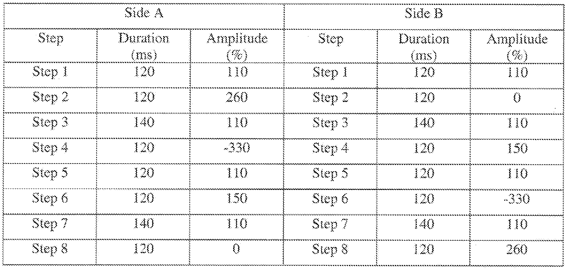
- the rectifier(s) is/are programmable with 8 steps which define a single set of pulse plating periods as further explained herein, which 8 steps may include, for example;
- Table 4 sets forth an example of a pulse plating cycle having 8 steps in accordance with the present invention.
- the box manifold/verticai pipes are designed to include the array of eductor nozzles or cone nozzles. Opposing nozzles are designed front to back side.
- the nozzles am preferably arranged in a staggered pattern and may be arranged about 2 to about 8 cm apart, more preferably about 3 to about 6 cm apart, most preferably about 4 to about 5 cm apart in both horizontal and vertical direction.
- An acid copper electrolyte was made up according to the following parameters:
- the concentration of copper sulfate was maintained with the addition of copper oxide, on either a manual or automatic basis, based on Amp hours of operation and/or with chemical titration analysis.
- the concentration of sulfuric add and chloride ions was replenished based on chemical titration analysis.
- Replenishment of the accelerator, suppressor, and secondary suppressor was accomplished with an automatic dosing system, based on Amp hours of operation and/or cyclic voltameiric stripping (CVS) analysis, A flash plating layer was deposited by DC plating at a current density of 2 ASD for a period of 10 minutes. Thereafter, pulse reverse plating was performed at a current density of 2.4 ASD for a period of 60 minutes to create a copper bridge in the through-holes, followed by DC plating at a current density of 2.5 ASD for a period of 60 minutes until the through-holes were filled in a vertical plating process.
- CVS cyclic voltameiric stripping
- the pulse plating waveform on a first side and a second side of the substrate followed a sequence of;
- a flash plating layer was deposited by DC plating at a current density of 2 ASD for a period of 10 minutes, Thereafter, pulse reverse plating was performed at a current density of 3.0 ASD for a period of 45 minutes to create a copper bridge in the through - holes, followed by DC plating at a current density of 2.0 ASD for 90 minutes until the through-holes were filled in a vertical plating process.
- the pulse plating waveform on a first side and a second side of the substrate followed a sequence of:
- An acid copper electrolyte was made up according to the following parameters:
- a flash plating layer was deposited by DC plating at a current density of 2 ASD for a period of 10 minutes. Thereafter, pulse reverse plating was performed at a current density of 2.4 ASD for a period of 40 minutes to create a copper bridge in the through-holes. Thereafter synchronous pulse plating was performed at a current density of 2.7 ASD for a period of 40 minutes to shape the bridge, followed by DC plating at a current density of 2.5 ASD for a period of 60 minutes until the through-holes were filled in a vertical plating process.
- the pulse plating waveform on a first side and a second side of the substrate in the bridging step followed a sequence of:
- the synchronous pulse plating in the shaping step had the following parameters:
- An acid copper electrolyte was made up as in Example 3.
- a flash plating layer was deposited by DC plating at a current density of 2 ASD for a period of 10 minutes. Thereafter, pulse reverse plating was performed at a current density of 2.4 ASD for a period of 40 minutes to create a copper bridge in the through-holes. Thereafter synchronous pulse plating was performed at a current density of 2.7 ASD for a period of 40 minutes to shape the bridge, followed by DC plating at a current density of 2.5 ASD for a period of 60 minutes until the through-holes were filled in a vertical plating process.
- the pulse plating waveform on a first side and a second side of the substrate followed a sequence of:
- the synchronous pulse plating in the shaping step had the following parameters:
Landscapes
- Chemical & Material Sciences (AREA)
- Engineering & Computer Science (AREA)
- Chemical Kinetics & Catalysis (AREA)
- Electrochemistry (AREA)
- Materials Engineering (AREA)
- Metallurgy (AREA)
- Organic Chemistry (AREA)
- Microelectronics & Electronic Packaging (AREA)
- Manufacturing & Machinery (AREA)
- Printing Elements For Providing Electric Connections Between Printed Circuits (AREA)
- Electroplating Methods And Accessories (AREA)
- Manufacturing Of Printed Wiring (AREA)
Abstract
Description




Claims
Priority Applications (5)
| Application Number | Priority Date | Filing Date | Title |
|---|---|---|---|
| US18/289,075 US12635082B2 (en) | 2021-05-17 | 2022-05-10 | Single step electrolytic method of filling through-holes in printed circuit boards and other substrates |
| CN202280041561.9A CN117480872A (en) | 2021-05-17 | 2022-05-10 | Single-step electrolytic method for filling through-holes in printed circuit boards and other substrates |
| EP22805186.8A EP4342269A4 (en) | 2021-05-17 | 2022-05-10 | Single-stage electrolytic process for filling through holes in printed circuit boards and other substrates |
| KR1020237042746A KR102996431B1 (en) | 2021-05-17 | 2022-05-10 | Single-step electrolytic method for filling through holes in printed circuit boards and other substrates |
| JP2023568671A JP2024519743A (en) | 2021-05-17 | 2022-05-10 | Single-step electrolytic method for filling through holes in printed circuit boards and other substrates |
Applications Claiming Priority (2)
| Application Number | Priority Date | Filing Date | Title |
|---|---|---|---|
| US202163189640P | 2021-05-17 | 2021-05-17 | |
| US63/189,640 | 2021-05-17 |
Publications (2)
| Publication Number | Publication Date |
|---|---|
| WO2022245576A1 true WO2022245576A1 (en) | 2022-11-24 |
| WO2022245576A9 WO2022245576A9 (en) | 2023-10-12 |
Family
ID=84141896
Family Applications (1)
| Application Number | Title | Priority Date | Filing Date |
|---|---|---|---|
| PCT/US2022/028462 Ceased WO2022245576A1 (en) | 2021-05-17 | 2022-05-10 | Single step electrolytic method of filling through holes in printed circuit boards and other substrates |
Country Status (7)
| Country | Link |
|---|---|
| US (1) | US12635082B2 (en) |
| EP (1) | EP4342269A4 (en) |
| JP (1) | JP2024519743A (en) |
| KR (1) | KR102996431B1 (en) |
| CN (1) | CN117480872A (en) |
| TW (1) | TWI816388B (en) |
| WO (1) | WO2022245576A1 (en) |
Cited By (1)
| Publication number | Priority date | Publication date | Assignee | Title |
|---|---|---|---|---|
| CN119194570A (en) * | 2024-11-29 | 2024-12-27 | 昆山科比精工设备有限公司 | A micro blind hole processing device for composite copper foil |
Families Citing this family (1)
| Publication number | Priority date | Publication date | Assignee | Title |
|---|---|---|---|---|
| TWI887974B (en) * | 2024-01-23 | 2025-06-21 | 財團法人工業技術研究院 | Electroplating apparatus |
Citations (6)
| Publication number | Priority date | Publication date | Assignee | Title |
|---|---|---|---|---|
| US20100219081A1 (en) * | 2007-05-21 | 2010-09-02 | C. Uyemura & Co., Ltd. | Copper electroplating bath |
| US7887693B2 (en) * | 2007-06-22 | 2011-02-15 | Maria Nikolova | Acid copper electroplating bath composition |
| US20150156888A1 (en) | 2013-11-29 | 2015-06-04 | Ibiden Co., Ltd. | Method for manufacturing printed wiring board |
| US20150289387A1 (en) * | 2011-12-21 | 2015-10-08 | Atotech Deutschland Gmbh | Method for combined through-hole plating and via filling |
| US20200080217A1 (en) | 2014-12-05 | 2020-03-12 | Atotech Deutschland Gmbh | Method and apparatus for electroplating a metal onto a substrate |
| US20210130970A1 (en) | 2019-11-05 | 2021-05-06 | Macdermid Enthone Inc. | Single Step Electrolytic Method of Filling Through Holes in Printed Circuit Boards and Other Substrates |
Family Cites Families (14)
| Publication number | Priority date | Publication date | Assignee | Title |
|---|---|---|---|---|
| US6524461B2 (en) * | 1998-10-14 | 2003-02-25 | Faraday Technology Marketing Group, Llc | Electrodeposition of metals in small recesses using modulated electric fields |
| US6368965B1 (en) * | 1999-03-26 | 2002-04-09 | Advanced Micro Devices, Inc. | Method for low stress plating of semiconductor vias and channels |
| JP2001267726A (en) | 2000-03-22 | 2001-09-28 | Toyota Autom Loom Works Ltd | Electroplating method for wiring board and electroplating apparatus for wiring board |
| US20050145499A1 (en) * | 2000-06-05 | 2005-07-07 | Applied Materials, Inc. | Plating of a thin metal seed layer |
| US6827833B2 (en) * | 2001-10-15 | 2004-12-07 | Faraday Technology Marketing Group, Llc | Electrodeposition of metals in high-aspect ratio cavities using modulated reverse electric fields |
| JP2003213489A (en) | 2002-01-15 | 2003-07-30 | Learonal Japan Inc | Via filling method |
| WO2007082112A2 (en) * | 2006-01-06 | 2007-07-19 | Faraday Technology, Inc. | Tin and tin alloy electroplating method with controlled internal stress and grain size of the resulting deposit |
| EP2000013B1 (en) * | 2006-03-30 | 2010-10-13 | ATOTECH Deutschland GmbH | Electrolytic method for filling holes and cavities with metals |
| KR20130001368A (en) | 2011-06-27 | 2013-01-04 | 안복만 | Light emitting device package and method of manufacturing the same |
| JP5980735B2 (en) * | 2012-08-07 | 2016-08-31 | 株式会社荏原製作所 | Through-hole electroplating method and electroplating apparatus |
| CN112210801A (en) * | 2019-07-09 | 2021-01-12 | 江西博泉化学有限公司 | Electroplating solution for electroplating through hole of circuit board with high aspect ratio and electroplating method thereof |
| TWI886143B (en) * | 2019-08-19 | 2025-06-11 | 德商德國艾托特克公司 | Manufacturing sequences for high density interconnect printed circuit boards and a high density interconnect printed circuit board |
| JP2022545091A (en) * | 2019-08-19 | 2022-10-25 | アトテック ドイチェランド ゲーエムベーハー ウント コ カーゲー | Method for manufacturing high density interconnect printed circuit board containing copper-filled microvias |
| CN111101174A (en) * | 2020-01-14 | 2020-05-05 | 广州精原环保科技有限公司 | Pulse electroplating method based on double-phase pulse |
-
2022
- 2022-05-09 TW TW111117308A patent/TWI816388B/en active
- 2022-05-10 JP JP2023568671A patent/JP2024519743A/en active Pending
- 2022-05-10 CN CN202280041561.9A patent/CN117480872A/en active Pending
- 2022-05-10 US US18/289,075 patent/US12635082B2/en active Active
- 2022-05-10 EP EP22805186.8A patent/EP4342269A4/en active Pending
- 2022-05-10 WO PCT/US2022/028462 patent/WO2022245576A1/en not_active Ceased
- 2022-05-10 KR KR1020237042746A patent/KR102996431B1/en active Active
Patent Citations (6)
| Publication number | Priority date | Publication date | Assignee | Title |
|---|---|---|---|---|
| US20100219081A1 (en) * | 2007-05-21 | 2010-09-02 | C. Uyemura & Co., Ltd. | Copper electroplating bath |
| US7887693B2 (en) * | 2007-06-22 | 2011-02-15 | Maria Nikolova | Acid copper electroplating bath composition |
| US20150289387A1 (en) * | 2011-12-21 | 2015-10-08 | Atotech Deutschland Gmbh | Method for combined through-hole plating and via filling |
| US20150156888A1 (en) | 2013-11-29 | 2015-06-04 | Ibiden Co., Ltd. | Method for manufacturing printed wiring board |
| US20200080217A1 (en) | 2014-12-05 | 2020-03-12 | Atotech Deutschland Gmbh | Method and apparatus for electroplating a metal onto a substrate |
| US20210130970A1 (en) | 2019-11-05 | 2021-05-06 | Macdermid Enthone Inc. | Single Step Electrolytic Method of Filling Through Holes in Printed Circuit Boards and Other Substrates |
Non-Patent Citations (1)
| Title |
|---|
| See also references of EP4342269A4 |
Cited By (1)
| Publication number | Priority date | Publication date | Assignee | Title |
|---|---|---|---|---|
| CN119194570A (en) * | 2024-11-29 | 2024-12-27 | 昆山科比精工设备有限公司 | A micro blind hole processing device for composite copper foil |
Also Published As
| Publication number | Publication date |
|---|---|
| EP4342269A1 (en) | 2024-03-27 |
| KR20240008885A (en) | 2024-01-19 |
| US12635082B2 (en) | 2026-05-19 |
| CN117480872A (en) | 2024-01-30 |
| JP2024519743A (en) | 2024-05-21 |
| WO2022245576A9 (en) | 2023-10-12 |
| KR102996431B1 (en) | 2026-07-28 |
| TW202308477A (en) | 2023-02-16 |
| TWI816388B (en) | 2023-09-21 |
| US20240224432A1 (en) | 2024-07-04 |
| EP4342269A4 (en) | 2025-10-29 |
Similar Documents
| Publication | Publication Date | Title |
|---|---|---|
| US11746433B2 (en) | Single step electrolytic method of filling through holes in printed circuit boards and other substrates | |
| US12325927B2 (en) | Complex waveform for electrolytic plating | |
| US6783654B2 (en) | Electrolytic plating method and device for a wiring board | |
| US6210555B1 (en) | Electrodeposition of metals in small recesses for manufacture of high density interconnects using reverse pulse plating | |
| US6863793B2 (en) | Sequential electrodeposition of metals using modulated electric fields for manufacture of circuit boards having features of different sizes | |
| CN101416569B (en) | Electrolytic method of filling holes and recesses with metal | |
| EP2796019B1 (en) | Method for combined through-hole plating and via filling | |
| US20030010642A1 (en) | Sequential electrodeposition of metals using modulated electric fields for manufacture of circuit boards having features of different sizes | |
| JP2005320631A (en) | Improved plating method | |
| US20030075450A1 (en) | Electrodeposition of metals in high-aspect ratio cavities using modulated reverse electric fields | |
| US12635082B2 (en) | Single step electrolytic method of filling through-holes in printed circuit boards and other substrates | |
| HK40102235A (en) | Single step electrolytic method of filling through holes in printed circuit boards and other substrates | |
| HK40102165A (en) | Complex waveform for electrolytic plating | |
| Nikolova et al. | New generation solution for micro via metallization and through hole plating | |
| Sun et al. | Application of CM-ECD Process for HDI PWBs |
Legal Events
| Date | Code | Title | Description |
|---|---|---|---|
| 121 | Ep: the epo has been informed by wipo that ep was designated in this application |
Ref document number: 22805186 Country of ref document: EP Kind code of ref document: A1 |
|
| WWE | Wipo information: entry into national phase |
Ref document number: 18289075 Country of ref document: US |
|
| WWE | Wipo information: entry into national phase |
Ref document number: 2023568671 Country of ref document: JP |
|
| WWE | Wipo information: entry into national phase |
Ref document number: 2301007470 Country of ref document: TH |
|
| ENP | Entry into the national phase |
Ref document number: 20237042746 Country of ref document: KR Kind code of ref document: A |
|
| WWE | Wipo information: entry into national phase |
Ref document number: 202280041561.9 Country of ref document: CN Ref document number: 1020237042746 Country of ref document: KR |
|
| WWE | Wipo information: entry into national phase |
Ref document number: 2022805186 Country of ref document: EP |
|
| NENP | Non-entry into the national phase |
Ref country code: DE |
|
| ENP | Entry into the national phase |
Ref document number: 2022805186 Country of ref document: EP Effective date: 20231218 |
|
| WWE | Wipo information: entry into national phase |
Ref document number: 11202308525U Country of ref document: SG |
|
| WWG | Wipo information: grant in national office |
Ref document number: 18289075 Country of ref document: US |