WO2022249644A1 - アンテナ、電子機器およびアンテナの製造方法 - Google Patents
アンテナ、電子機器およびアンテナの製造方法 Download PDFInfo
- Publication number
- WO2022249644A1 WO2022249644A1 PCT/JP2022/010606 JP2022010606W WO2022249644A1 WO 2022249644 A1 WO2022249644 A1 WO 2022249644A1 JP 2022010606 W JP2022010606 W JP 2022010606W WO 2022249644 A1 WO2022249644 A1 WO 2022249644A1
- Authority
- WO
- WIPO (PCT)
- Prior art keywords
- antenna
- reflecting mirror
- parabolic
- primary radiator
- mirror
- Prior art date
- Legal status (The legal status is an assumption and is not a legal conclusion. Google has not performed a legal analysis and makes no representation as to the accuracy of the status listed.)
- Ceased
Links
Images


Classifications
-
- H—ELECTRICITY
- H01—ELECTRIC ELEMENTS
- H01Q—ANTENNAS, i.e. RADIO AERIALS
- H01Q15/00—Devices for reflection, refraction, diffraction or polarisation of waves radiated from an antenna, e.g. quasi-optical devices
- H01Q15/14—Reflecting surfaces; Equivalent structures
- H01Q15/16—Reflecting surfaces; Equivalent structures curved in two dimensions [2D], e.g. paraboloidal
-
- H—ELECTRICITY
- H01—ELECTRIC ELEMENTS
- H01Q—ANTENNAS, i.e. RADIO AERIALS
- H01Q1/00—Details of, or arrangements associated with, antennas
- H01Q1/27—Adaptation for use in or on movable bodies
- H01Q1/28—Adaptation for use in or on aircraft, missiles, satellites, or balloons
-
- H—ELECTRICITY
- H01—ELECTRIC ELEMENTS
- H01Q—ANTENNAS, i.e. RADIO AERIALS
- H01Q1/00—Details of, or arrangements associated with, antennas
- H01Q1/40—Radiating elements coated with or embedded in protective material
-
- H—ELECTRICITY
- H01—ELECTRIC ELEMENTS
- H01Q—ANTENNAS, i.e. RADIO AERIALS
- H01Q15/00—Devices for reflection, refraction, diffraction or polarisation of waves radiated from an antenna, e.g. quasi-optical devices
- H01Q15/14—Reflecting surfaces; Equivalent structures
-
- H—ELECTRICITY
- H01—ELECTRIC ELEMENTS
- H01Q—ANTENNAS, i.e. RADIO AERIALS
- H01Q15/00—Devices for reflection, refraction, diffraction or polarisation of waves radiated from an antenna, e.g. quasi-optical devices
- H01Q15/14—Reflecting surfaces; Equivalent structures
- H01Q15/141—Apparatus or processes specially adapted for manufacturing reflecting surfaces
-
- H—ELECTRICITY
- H01—ELECTRIC ELEMENTS
- H01Q—ANTENNAS, i.e. RADIO AERIALS
- H01Q19/00—Combinations of primary active antenna elements and units with secondary devices, e.g. with quasi-optical devices, for giving the antenna a desired directional characteristic
- H01Q19/10—Combinations of primary active antenna elements and units with secondary devices, e.g. with quasi-optical devices, for giving the antenna a desired directional characteristic using reflecting surfaces
- H01Q19/12—Combinations of primary active antenna elements and units with secondary devices, e.g. with quasi-optical devices, for giving the antenna a desired directional characteristic using reflecting surfaces wherein the surfaces are concave
-
- H—ELECTRICITY
- H01—ELECTRIC ELEMENTS
- H01Q—ANTENNAS, i.e. RADIO AERIALS
- H01Q19/00—Combinations of primary active antenna elements and units with secondary devices, e.g. with quasi-optical devices, for giving the antenna a desired directional characteristic
- H01Q19/10—Combinations of primary active antenna elements and units with secondary devices, e.g. with quasi-optical devices, for giving the antenna a desired directional characteristic using reflecting surfaces
- H01Q19/12—Combinations of primary active antenna elements and units with secondary devices, e.g. with quasi-optical devices, for giving the antenna a desired directional characteristic using reflecting surfaces wherein the surfaces are concave
- H01Q19/17—Combinations of primary active antenna elements and units with secondary devices, e.g. with quasi-optical devices, for giving the antenna a desired directional characteristic using reflecting surfaces wherein the surfaces are concave the primary radiating source comprising two or more radiating elements
-
- H—ELECTRICITY
- H01—ELECTRIC ELEMENTS
- H01Q—ANTENNAS, i.e. RADIO AERIALS
- H01Q21/00—Antenna arrays or systems
- H01Q21/24—Combinations of antenna units polarised in different directions for transmitting or receiving circularly and elliptically polarised waves or waves linearly polarised in any direction
- H01Q21/26—Turnstile or like antennas comprising arrangements of three or more elongated elements disposed radially and symmetrically in a horizontal plane about a common centre
Definitions
- the present invention relates to technology for antennas mounted on flying objects such as rockets and aircraft.
- Antennas mounted on flying objects such as rockets and aircraft are required to radiate radio waves uniformly over a wide area and to withstand aerodynamic loads and aerodynamic heating that occur during flight.
- the inventor of the present invention proposed the antenna shown in Patent Document 1.
- the antenna of Patent Document 1 comprises a primary radiator and a parabolic reflector.
- the antenna pattern in the hemisphere where radio waves are radiated does not generate null points, and the antenna is uniformly stable over a wide range. pattern characteristics can be obtained.
- the aperture diameter of the parabolic reflector is as small as 1.7 times or less of the wavelength, so the primary radiator is very close to the parabolic reflector compared to a general parabolic antenna. is installed. Therefore, the impedance characteristic of the primary radiator is strongly affected by the reflector, and it becomes impossible to arbitrarily change the impedance characteristic of the primary radiator.
- an object of the present invention is to manufacture an antenna, an electronic device, and an antenna that can arbitrarily change the impedance characteristics of a primary radiator while maintaining a uniform and stable pattern characteristic over a wide range. It is to provide a method.
- An antenna includes a primary radiator and a reflector.
- the primary radiator radiates radio waves.
- the reflector reflects the radio waves emitted from the primary radiator, has an aperture diameter and height equal to those of a parabolic reflector whose aperture diameter is 1.7 times or less the wavelength of the radio waves, and has a non-parabolic mirror surface shape. It is the surface.
- the antenna pattern in the hemisphere from which the radio wave is radiated does not generate a null point, and a wide range can be obtained. uniform and stable pattern characteristics can be obtained.
- the reflector of the antenna of Patent Document 1 is a parabolic reflector, that is, a reflector with a paraboloid of revolution
- the shape of the reflector is determined by the aperture diameter and height.
- an antenna according to one aspect of the present invention employs a non-parabolic reflector having a shape other than a paraboloid of revolution. That is, the aperture diameter and height of the reflecting mirror are the same as those of the parabolic reflecting mirror, but the shape of the mirror surface is changed from the paraboloid of revolution.
- the primary radiator can have an impedance characteristic different from the impedance characteristic of the primary radiator obtained when the reflecting mirror is parabolic.
- the impedance of the antenna according to one embodiment of the present invention can be narrower or wider than the impedance of the antenna described in Patent Document 1 in the frequency band in which matching with the feeding system can be achieved.
- the non-parabolic surface may have a shape in which the height from the bottom of the mirror surface of the reflecting mirror is proportional to the power of the distance from the center axis of the reflecting mirror, excluding 2.
- the non-parabolic surface may be a truncated conical surface, a partial spherical surface, a conical surface, a cylindrical surface, or the like.
- the non-parabolic surface may have a shape obtained by combining two or more different shapes of non-parabolic surfaces.
- the primary radiator may be arranged in a region inside the opening surface of the reflecting mirror.
- the reflecting mirror may have a dielectric layer filled in a region inside the opening surface of the reflecting mirror.
- An electronic device has a configuration in which the antenna is embedded in a cavity provided on the surface of the antenna on the mounting side or inside the mounting side.
- the antenna By making a hole with the same shape and size as a parapolar reflector on the surface of the mounting side or inside the mounting side, the antenna can be installed without protruding from the surface of the mounting side. As a result, in the case of flying objects such as rockets and aircraft, the aerodynamic load and heating are greatly reduced. Since the antenna according to one aspect of the present invention has a small aperture diameter, the impact on flying objects caused by drilling a hole is reduced to a negligible level.
- the antenna according to one embodiment of the present invention is mounted inside or outside a building or an electronic device having a wireless communication function such as a PC, for example, a substrate for mounting electronic components, an outer wall of a building, an indoor wall or ceiling
- the antenna can be installed without protruding from the surface by making a hole of the same shape and size as the parapolar reflector on the surface of the antenna or inside the mounted side. can. Therefore, the antenna can be made thinner and lighter than the conventional rod-shaped antenna, etc., and the antenna gain is high because the parabolic antenna is used as the basic structure.
- the aperture surface the same color and pattern as the walls and ceiling, it is possible to make the antenna inconspicuous.
- a method for manufacturing an antenna according to one aspect of the present invention is designed to reflect radio waves emitted from a primary radiator and to design a reflecting mirror whose mirror surface has a parabolic surface and whose aperture diameter is 1.7 times or less the wavelength of the radio waves.
- the mirror surface is modified to a non-parabolic surface having the same aperture diameter and height as the parabolic surface.
- the present invention it is possible to arbitrarily change the impedance characteristics of the primary radiator while maintaining stable pattern characteristics over a wide range.
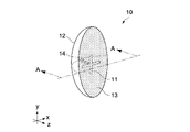
- FIG. 1 is a perspective view showing the configuration of an antenna according to one embodiment of the present invention
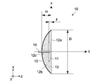
- FIG. FIG. 2 is a cross-sectional view taken along the line AA of FIG. 1
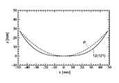
- FIG. 4 is a diagram for explaining an embodiment of the above antenna, and is a cross-sectional view showing a shape in which the height of the reflecting mirror surface from the bottom of the mirror surface is proportional to the power of the distance from the central axis excluding 2
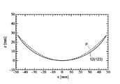
- FIG. 4 is a diagram for explaining an embodiment of the antenna, and is a cross-sectional view in which the reflecting mirror has a truncated cone shape.
- FIG. 4 is a diagram for explaining an embodiment of the antenna, and is a cross-sectional view in which the reflecting mirror has a partially spherical shape.
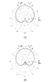
- FIG. 10 is a diagram illustrating an embodiment of the above antenna, showing the pattern of the antenna when the shape of the reflector is proportional to the power of the distance from the central axis except for the height of the reflector surface from the bottom of the mirror surface (right-handed Analytical values of polarized waves) are displayed in the xz plane.
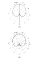
- FIG. 10 is a diagram for explaining an embodiment of the above antenna, showing the analytical values of the antenna pattern (right-handed polarization) in the xz plane when the shape of the reflecting mirror is a truncated cone.
- FIG. 10 is a diagram for explaining an embodiment of the above antenna, showing the analytical values of the antenna pattern (right-handed polarization) in the xz plane when the shape of the reflecting mirror is a partial sphere.
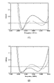
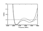
- FIG. 4 is a diagram for explaining an embodiment of the above antenna, and is a diagram showing an analytical value of VSWR with respect to 50 ⁇ , which indicates the impedance characteristic of the primary radiator when the reflecting mirror has a truncated conical shape, as a frequency characteristic.
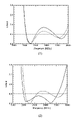
- FIG. 4 is a diagram for explaining an embodiment of the above antenna, and is a diagram showing an analytical value of VSWR with respect to 50 ⁇ , which indicates the impedance characteristic of the primary radiator when the reflecting mirror has a truncated conical shape, as a frequency characteristic.
- FIG. 10 is a diagram for explaining an embodiment of the above antenna, and shows an analytical value of VSWR with respect to 50 ⁇ , which indicates the impedance characteristic of the primary radiator when the shape of the reflector is a partial spherical shape, as a frequency characteristic.
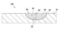
- 1 is a cross-sectional view of an electronic device equipped with an antenna according to an embodiment of the present invention
- FIG. 1 is a perspective view showing the configuration of an antenna 10 according to one embodiment of the present invention
- FIG. 2 is a cross-sectional view taken along line AA of FIG.
- the x-axis, y-axis and z-axis indicate three mutually orthogonal directions
- the z-axis corresponds to the central axis of the reflector 12 of the antenna 10 .
- antenna 10 has primary radiator 11 and reflector 12 .
- Antenna 10 further includes a dielectric layer 13 filled in a region inside from opening surface 12 a of reflector 12 , and a feeding cable 14 connected to primary radiator 11 .
- the antenna 10 of the present embodiment is mounted on, for example, a flying object such as a rocket or an aircraft.
- the primary radiator 11 is an antenna element that radiates radio waves. Any antenna element can be used as the primary radiator 11 as long as it can obtain a predetermined impedance. In this embodiment, an example using a cross dipole antenna is shown, but a dipole antenna, a horn antenna, or the like can also be used.
- the reflecting mirror 12 has a shape (non-parabolic surface) different from a paraboloid of revolution (parabolic surface) having a diameter (opening diameter) of the opening surface 12a of D and a height of H from the mirror bottom 12c to the opening surface 12a.
- the primary radiator 11 is arranged at a depth F from the opening surface 12a of the reflector 12. As shown in FIG.
- the reflecting mirror 12 reflects the radio waves emitted from the primary radiator 11, and the aperture diameter D is made smaller than the aperture diameter at which null points do not occur in the hemispherical antenna pattern in which the radio waves are reflected and radiated. ing.
- the reflecting mirror 12 has an aperture diameter D that is 1.7 times or less the wavelength of radio waves.
- the aperture diameter D and the dimensions of the primary radiator 11 can be made small to the extent that they function as an antenna.
- the range in which the primary radiator 11 functions as an antenna is the range in which the primary radiator 11 can obtain a predetermined impedance. . Since no null point occurs in the antenna 10 according to this embodiment, naturally no side lobe occurs. That is, the antenna 10 according to this embodiment can radiate uniform radio waves over a wide range within the hemisphere from which the radio waves are radiated.
- the dielectric layer 13 is filled in a range from the opening surface 12a of the reflecting mirror 12 to the mirror surface 12b, which is the inner surface of the reflecting mirror 12.
- the dielectric material forming the dielectric layer 13 is not particularly limited, and synthetic resin materials such as high-density polyethylene and polytetrafluoroethylene are used, for example.
- the dielectric constant of the dielectric is also not particularly limited, and can be arbitrarily set according to the type and specifications of the mounted object on which the antenna 10 is installed.
- the primary radiator 11 is arranged within the dielectric layer 13 .
- the primary radiator 11 is arranged at the position of the opening surface 12a or at a position inside thereof.
- the feeder cable 14 is a coaxial cable that feeds the primary radiator 11 . 1 and 2 show an example in which the power supply cable 14 is routed from the mirror bottom 12c to the primary radiator 11, but the power supply cable 14 may be routed in any way within the reflector 12. .
- the dielectric layer 13 has the function of holding the primary radiator 11 and the power supply cable 14 at predetermined positions. In addition, the dielectric layer 13 has the function of protecting them from aerodynamic loads and aerodynamic heating generated during flight of a rocket or the like, and the wavelength shortening effect of the dielectric enables further miniaturization of the antenna 10. do. Dielectric layer 13 may have a cavity (not shown). Thereby, the weight of the antenna 10 can be reduced.
- the antenna 10 has a radio wave frequency of 2.28 GHz
- the primary radiator 11 and the reflector 12 are made of copper
- the dielectric layer 13 is filled with high-density polyethylene
- the aperture diameter D is 96 mm
- the reflector The height H of 12 was set to 28 mm
- the depth F from the opening surface 12a to the primary radiator 11 was set to 7 mm. Since the wavelength is approximately 132 mm, the aperture diameter D is approximately 0.73 wavelength.
- the reflecting mirror 12 has the same opening diameter and height as the parabolic reflecting mirror, and the shape of the mirror surface 12b is a non-parabolic surface.
- the aperture diameter and height of the parabolic reflector correspond to the aperture diameter D and height H of the reflector 12, respectively.
- the aperture diameter D is 1.7 times or less the wavelength of radio waves emitted from the primary radiator 11 as described above.
- the reflecting mirror 12 in the antenna 10 of this embodiment has the same aperture diameter and height as the parabolic reflecting mirror, but differs in that the shape of the mirror surface 12b is a non-parabolic surface.
- the non-parabolic surface is, for example, (1) a shape in which the height of the mirror surface 12b from the mirror surface bottom 12c is proportional to the power of the distance from the central axis (z-axis) of the reflecting mirror 12 excluding 2, and (2) a truncated cone surface. , (3) partial spherical surface, (4) conical surface, (5) cylindrical surface, etc.
- the non-parabolic surface may have a shape obtained by arbitrarily combining two or more of the above (1) to (5). Also, any value from 1 to 3 (excluding 2), for example, can be applied to the power exponent in (1) above.
- FIG. 3 shows the mirror surface shape (solid line in the figure) of the reflector 12 in the antenna 10 according to one embodiment of the present invention, and the mirror surface shape (dotted line in the figure) of the parabolic reflector P having the same aperture diameter D and height H. ) is a cross-sectional view in the xz plane shown in comparison with FIG.
- a reflecting mirror 121 having a mirror surface shape corresponding to (1) above is shown.
- FIG. 4 shows the mirror surface shape (solid line in the figure) of the reflector 12 in the antenna 10 according to another embodiment of the present invention, and the mirror surface shape (dotted line in the figure) of the parabolic reflector P having the same aperture diameter D and height H. ) is a cross-sectional view in the xz plane shown in comparison with FIG.
- a reflecting mirror 122 having a mirror surface shape corresponding to (2) above is shown.
- FIG. 5 shows the mirror surface shape (solid line in the figure) of the reflector 12 in the antenna 10 according to still another embodiment of the present invention, and the mirror surface shape ( 2 is a cross-sectional view in the xz plane shown in comparison with the dotted line).
- the reflecting mirror 12 a reflecting mirror 123 having a mirror surface shape corresponding to (3) above is shown.
- Fig. 3 shows analytical values of the antenna pattern (right-handed polarized wave) of the antenna 10 in the xz plane. (1) and (2) of the same figure show the cases where the height of the mirror surface 12b from the mirror surface bottom 12c is proportional to the distance from the central axis to the 1.5th power and the 3.0th power, respectively.
- the antenna pattern of the antenna 10 according to this embodiment almost matches the antenna pattern of the antenna of Patent Document 1 above the antenna aperture plane.
- This is an in-plane display.
- (1) and (2) of the figure show the case where the opening diameters of the bottom surface of the mirror surface 12b are 24 mm and 48 mm, respectively.
- FIG. 7 it can be seen that the antenna pattern of the antenna 10 according to this embodiment almost matches the antenna pattern of the antenna of Patent Document 1 above the antenna aperture plane.
- This is an in-plane display.
- FIG. 8 it can be seen that the antenna pattern of the antenna 10 according to this embodiment almost matches the antenna pattern of the antenna of Patent Document 1 above the antenna aperture plane.
- 2 shows the analytical value of VSWR with respect to 50 ⁇ , which indicates the impedance characteristic of the primary radiator 11 in the antenna 10, as a frequency characteristic.
- (1) and (2) of the same figure show the cases where the height of the mirror surface 12b from the mirror surface bottom 12c is proportional to the distance from the central axis to the 1.5th power and the 3.0th power, respectively.
- the analysis values are displayed as frequency characteristics.
- (1) and (2) of the figure show the case where the opening diameters of the bottom surface of the mirror surface 12b are 24 mm and 48 mm, respectively.
- VSWR analysis for 50 ⁇ values are displayed as frequency characteristics.
- the antenna 10 of the present embodiment configured as described above is designed as a reflector having a parabolic surface whose aperture diameter is 1.7 times or less the wavelength of radio waves. Manufactured by modifying the specular surface to an equal non-parabolic surface.
- non-parabolic surface in addition to a shape in which the height from the bottom of the mirror surface of the reflecting mirror is proportional to the power of the distance from the central axis of the reflecting mirror excluding 2, a truncated cone surface, a partial spherical surface, a conical surface, An arbitrary shape such as a cylindrical surface can be adopted according to the impedance characteristics of the feeding system of the primary radiator 11 and the like.
- Modification of the mirror surface to a non-parabolic surface involves changing the shape of the mirror surface formed on the parabolic surface by machining, etc., to a non-parabolic surface, or designing in order to narrow or widen the frequency band that can be matched with the feed system. Any method such as changing the parabolic surface to a non-parabolic surface in the process of .
- the antenna 10 since the reflector 12 has an aperture diameter D that is 1.7 times or less the wavelength of radio waves, the antenna pattern in the hemisphere from which radio waves are radiated has a null point. It is possible to obtain uniform and stable pattern characteristics over a wide range without causing such occurrence (see FIG. 4 of Patent Document 1). More specifically, the following effects can be obtained.
- ⁇ Antenna beam spreads and radio waves are radiated over a wide area. There is also radiation downward from the antenna aperture plane. - There are no null points or dips in the hemisphere above the antenna aperture. ⁇ Because it is a reflector antenna, the antenna pattern is almost unaffected by the shape of the mounting side and the antenna mounting part.
- ⁇ It has a uniform and stable pattern characteristic over a wide range, and the gain is higher than that of the antennas currently mounted on flying objects.
- the mounted side which is the flying object, is not subject to operation restrictions due to pattern characteristics.
- the aerodynamic load and heating generated in the antenna 10 are greatly reduced. ⁇ Compared to conventional antennas, it can be made thinner and lighter, making it more inconspicuous.
- the antenna is installed without protruding from the surface of the mounting side by opening a hole having the same shape and size as the parapolar reflector on the surface of the mounting side or inside the mounting side. be able to.
- the aerodynamic load and heating are greatly reduced. Since the antenna according to this embodiment has a small aperture diameter, the impact on the flying object caused by drilling the hole is reduced to a negligible level.
- the antenna according to one embodiment of the present invention is mounted inside or outside a building or an electronic device having a wireless communication function such as a PC, for example, a substrate for mounting electronic components, an outer wall of a building, an indoor wall or ceiling
- the antenna can be installed without protruding from the surface by making a hole of the same shape and size as the parapolar reflector on the surface of the antenna or inside the mounted side. can. Therefore, the antenna can be made thinner and lighter than the conventional rod-shaped antenna, etc., and the antenna gain is high because the parabolic antenna is used as the basic structure.
- the aperture surface the same color and pattern as the walls and ceiling, it is possible to make the antenna inconspicuous.
- the mirror surface shape is a non-parabolic surface. It is possible to change the impedance characteristics of the primary radiator. More specifically, the frequency band in which impedance matching with the feeding system of the primary radiator 11 can be achieved can be made narrower or wider than the antenna described in Patent Document 1.
- the frequency band in which impedance matching with the feeding system of the primary radiator 11 can be achieved is narrowed, it becomes unnecessary to prepare a filter for blocking radio waves of the frequency to be removed.
- FIG. 12 is a fragmentary cross-sectional view of an electronic device 100 according to another embodiment of the invention.
- Electronic device 100 includes substrate 91 and antenna 90 embedded in the surface of substrate 91 .
- a substrate 91 is provided with a hole 92 that matches the shape of the reflector, and a conductive thin film 96 is formed on the surface of the hole 92 .
- the conductive thin film 96 functions as a reflector for the antenna 90 .
- a region inside the opening surface of the hole 92 is filled with a dielectric layer 93 made of a dielectric such as high-density polyethylene.
- a primary radiator 94 of the antenna 90 is placed on the opening surface of the hole 92 and held by the dielectric layer 93 .
- the hole 92 corresponds to a cavity provided on the surface of the mounted side of the antenna 90 or inside the mounted side, and the antenna 90 is embedded in this cavity.
- the hole 92 has the same opening diameter and height as the parabolic reflector, but the shape is formed with a non-parabolic surface. Accordingly, the conductive thin film 96 formed on the surface of the hole 92 forms a non-parabolic mirror surface.
- the opening diameter of the hole 92 (the conductive thin film 96) is such that the radio wave radiated from the primary radiator 94 is reflected by the reflecting mirror portion and radiated, and the antenna pattern in the hemisphere does not have a null point (wavelength). 1.7 times or less).
- Feed cable 95 is held by dielectric layer 93 and connected to primary radiator 94 .
- the antenna 90 is composed of the hole 92 in which the conductive thin film 96 is formed, the dielectric layer 93 and the primary radiator 94 .
- the antenna 90 can be installed without protruding from the surface of the substrate 91, and the footprint of the antenna 90 can be reduced because the opening diameter of the antenna 90 is small. Therefore, the antenna can be made thinner and lighter than the conventional rod-shaped antenna, etc., and the antenna gain is high because the reflector antenna is used as the basic structure.
- the frequency band that can be matched with the feeding system is narrower than the impedance of the antenna having the parabolic reflector described in Patent Document 1. Alternatively, it can be arbitrarily adjusted such as widening.
- the present invention is applied to an antenna mounted on a flying object such as a rocket or an aircraft. It can also be applied to equipment and buildings.
- a flying object such as a rocket or an aircraft.
- the antenna according to the present invention is installed outside or inside a building, it is possible to make the antenna inconspicuous by making the opening surface of the antenna the same color and pattern as the walls and ceiling of the building.
Landscapes
- Physics & Mathematics (AREA)
- Electromagnetism (AREA)
- Engineering & Computer Science (AREA)
- Astronomy & Astrophysics (AREA)
- Aviation & Aerospace Engineering (AREA)
- General Physics & Mathematics (AREA)
- Remote Sensing (AREA)
- Manufacturing & Machinery (AREA)
- Aerials With Secondary Devices (AREA)
- Details Of Aerials (AREA)
- Support Of Aerials (AREA)
Abstract
Description
前記一次放射器は、電波を放射する。
前記反射鏡は、前記一次放射器より放射された電波を反射し、開口径が前記電波の波長の1.7倍以下であるパラボラ反射鏡と開口径および高さが等しく、鏡面形状が非パラボラ面である。
あるいは、前記非パラボラ面は、円錐台面、部分球面、円錐面、円筒面などであってもよい。
あるいは、前記非パラボラ面は、2以上の異なる形状の非パラボラ面を組み合わせた形状であってもよい。
前記パラボラ面と開口径および高さが等しい非パラボラ面に前記鏡面を修正する。
図1は、本発明の一実施形態に係るアンテナ10の構成を示す斜視図であり、図2は、図1のA-A断面図である。各図において、x軸、y軸およびz軸は相互に直交する3軸方向を示しており、z軸はアンテナ10の反射鏡12の中心軸に相当する。
図1及び図2に示すように、アンテナ10は、一次放射器11と、反射鏡12とを有する。アンテナ10はさらに、反射鏡12の開口面12aから内側の領域に充填された誘電体層13と、一次放射器11に接続される給電ケーブル14とを有する。本実施形態のアンテナ10は、例えば、ロケット、航空機等の飛翔体に搭載される。
反射鏡12は、パラボラ反射鏡と開口径および高さが等しく、鏡面12bの形状が非パラボラ面である。上記パラボラ反射鏡の開口径および高さは、それぞれ、反射鏡12の開口径Dおよび高さHに相当する。開口径Dは、上述のように一次放射器11から放射される電波の波長の1.7倍以下である。
図6に示すように、本実施形態に係るアンテナ10のアンテナパターンは、特許文献1のアンテナのアンテナパターンとアンテナ開口面よりも上方でほとんど一致することがわかる。
図7に示すように、本実施形態に係るアンテナ10のアンテナパターンは、特許文献1のアンテナのアンテナパターンとアンテナ開口面よりも上方でほとんど一致することがわかる。
図8に示すように、本実施形態に係るアンテナ10のアンテナパターンは、特許文献1のアンテナのアンテナパターンとアンテナ開口面よりも上方でほとんど一致することがわかる。
以上のように構成される本実施形態のアンテナ10は、開口径が電波の波長の1.7倍以下である鏡面がパラボラ面の反射鏡を設計し、上記パラボラ面と開口径および高さが等しい非パラボラ面に鏡面を修正することで製造される。
以上のように本実施形態に係るアンテナ10によれば、反射鏡12が電波の波長の1.7倍以下の開口径Dを有するため、電波が放射される半球内のアンテナパターンにヌル点を発生させることなく、広範囲に均一に安定したパターン特性を得ることができる(特許文献1の図4参照)。より具体的には、以下の作用を得ることができる。
・アンテナ開口面より上方の半球内にヌル点や落ち込みが存在しない。
・反射鏡アンテナであるため、アンテナパターンはアンテナを搭載する被搭載側の形状やアンテナ取付部の影響をほとんど受けない。
・広範囲に均一に安定したパターン特性を有し、現在飛翔体に搭載されているアンテナと比較すると利得も高くなる。
・アンテナ10が飛翔体に搭載される場合に、飛翔体である被搭載側でパターン特性からの運用制約を受けることがなくなる。
・アンテナ10を飛翔体に搭載する場合に、アンテナ10に発生する空力荷重・加熱が大幅に軽減される。
・従来のアンテナと比べて薄型軽量化でき、より目立たなくなる。
図12は本発明の他の実施形態に係る電子機器100の要部断面図である。電子機器100は、基板91と、基板91の表面に埋め込まれたアンテナ90とを備える。
11,94…一次放射器
12,121,122,123…反射鏡
12a…開口面
12b…鏡面
12c…鏡面底部
13,93…誘電体層
92…穴(空洞)
100…電子機器
Claims (7)
- 電波を放射する一次放射器と、
前記一次放射器より放射された電波を反射し、開口径が前記電波の波長の1.7倍以下であるパラボラ反射鏡と開口径および高さが等しく、鏡面形状が非パラボラ面である反射鏡と
を具備し、
前記一次放射器は、前記反射鏡の開口面から内側の領域に配置され、
前記反射鏡は、前記電波が反射して放射される半球内のアンテナパターンにヌル点が発生しないパターン特性を有する
アンテナ。 - 請求項1に記載のアンテナであって、
前記非パラボラ面は、2以上の異なる形状の非パラボラ面を組み合わせた形状である
アンテナ。 - 請求項1又は2に記載のアンテナであって、
前記非パラボラ面は、前記反射鏡の鏡面底部からの高さが前記反射鏡の中心軸からの距離の2を除くべき乗に比例する形状、円錐台面、部分球面、円錐面若しくは円筒面、又はこれらのうち2以上を組み合わせた形状である
アンテナ。 - 請求項1~3のいずれか1つに記載のアンテナであって、
前記反射鏡は、前記反射鏡の開口面から内側の領域に充填された誘電体層を有する
アンテナ。 - 請求項1~4のいずれか1つに記載のアンテナの被搭載側の表面、又は被搭載側の内部に設けられた空洞に、前記アンテナが埋め込まれた
電子機器。 - 一次放射器より放射された電波を反射し、開口径が前記電波の波長の1.7倍以下である鏡面がパラボラ面の反射鏡を設計し、
前記パラボラ面と開口径および高さが等しく、前記反射鏡の鏡面底部からの高さが前記反射鏡の中心軸からの距離の2を除くべき乗に比例する形状の非パラボラ面に前記鏡面を修正する
アンテナの製造方法であって、
前記一次放射器を前記反射鏡の開口面から内側の領域に配置し、
前記べき乗の値を変更することで、前記一次放射器の給電系とインピーダンス整合がとれる周波数帯域を前記パラボラ面の反射鏡よりも狭く又は広くする
アンテナの製造方法。 - 一次放射器より放射された電波を反射し、開口径が前記電波の波長の1.7倍以下である鏡面がパラボラ面の反射鏡を設計し、
前記パラボラ面と開口径および高さが等しい円錐台面形状の非パラボラ面に前記鏡面を修正する
アンテナの製造方法であって、
前記一次放射器を前記反射鏡の開口面から内側の領域に配置し、
前記鏡面の底面の開口径を変更することで、前記一次放射器の給電系とインピーダンス整合がとれる周波数帯域を前記パラボラ面の反射鏡よりも狭く又は広くする
アンテナの製造方法。
Priority Applications (5)
| Application Number | Priority Date | Filing Date | Title |
|---|---|---|---|
| EP22773095.9A EP4350893A4 (en) | 2021-05-27 | 2022-03-10 | ANTENNA, ELECTRONIC DEVICE AND METHOD FOR MANUFACTURING AN ANTENNA |
| KR1020227043883A KR102757029B1 (ko) | 2021-05-27 | 2022-03-10 | 안테나, 전자기기 및 안테나의 제조 방법 |
| US17/907,566 US12255397B2 (en) | 2021-05-27 | 2022-03-10 | Antenna, electronic apparatus, and method of manufacturing an antenna |
| CA3172568A CA3172568A1 (en) | 2021-05-27 | 2022-03-10 | Antenna, electronic apparatus, and method of manufacturing an antenna |
| AU2022231768A AU2022231768B2 (en) | 2021-05-27 | 2022-03-10 | Antenna, electronic apparatus, and method of manufacturing an antenna |
Applications Claiming Priority (2)
| Application Number | Priority Date | Filing Date | Title |
|---|---|---|---|
| JP2021089062A JP7029202B1 (ja) | 2021-05-27 | 2021-05-27 | アンテナ、電子機器およびアンテナの製造方法 |
| JP2021-089062 | 2021-05-27 |
Publications (1)
| Publication Number | Publication Date |
|---|---|
| WO2022249644A1 true WO2022249644A1 (ja) | 2022-12-01 |
Family
ID=81940844
Family Applications (1)
| Application Number | Title | Priority Date | Filing Date |
|---|---|---|---|
| PCT/JP2022/010606 Ceased WO2022249644A1 (ja) | 2021-05-27 | 2022-03-10 | アンテナ、電子機器およびアンテナの製造方法 |
Country Status (7)
| Country | Link |
|---|---|
| US (1) | US12255397B2 (ja) |
| EP (1) | EP4350893A4 (ja) |
| JP (1) | JP7029202B1 (ja) |
| KR (1) | KR102757029B1 (ja) |
| AU (1) | AU2022231768B2 (ja) |
| CA (1) | CA3172568A1 (ja) |
| WO (1) | WO2022249644A1 (ja) |
Families Citing this family (1)
| Publication number | Priority date | Publication date | Assignee | Title |
|---|---|---|---|---|
| JP7374525B1 (ja) | 2022-05-23 | 2023-11-07 | 国立研究開発法人宇宙航空研究開発機構 | アンテナおよび電子機器 |
Citations (4)
| Publication number | Priority date | Publication date | Assignee | Title |
|---|---|---|---|---|
| JPH03179903A (ja) * | 1989-12-08 | 1991-08-05 | Toshiba Corp | 鏡面修整アンテナ |
| JP2011505777A (ja) * | 2007-12-04 | 2011-02-24 | コンヴァートパワー リミテッド | エネルギを送受するための反射器を設計および製造するための新規の方法およびこの方法によって製造される反射器 |
| JP2020120153A (ja) | 2019-01-18 | 2020-08-06 | 国立研究開発法人宇宙航空研究開発機構 | アンテナ |
| JP2020536409A (ja) * | 2017-09-29 | 2020-12-10 | スター メッシュ エルエルシーStar Mesh Llc | 高利得アンテナを有するノードを用いる無線システム |
Family Cites Families (2)
| Publication number | Priority date | Publication date | Assignee | Title |
|---|---|---|---|---|
| JPH03141707A (ja) * | 1989-10-27 | 1991-06-17 | Yagi Antenna Co Ltd | 小形ヘリカルアンテナを用いた一次放射器 |
| US7710340B2 (en) | 2006-01-13 | 2010-05-04 | Lockheed Martin Corporation | Reconfigurable payload using non-focused reflector antenna for HIEO and GEO satellites |
-
2021
- 2021-05-27 JP JP2021089062A patent/JP7029202B1/ja active Active
-
2022
- 2022-03-10 US US17/907,566 patent/US12255397B2/en active Active
- 2022-03-10 AU AU2022231768A patent/AU2022231768B2/en active Active
- 2022-03-10 CA CA3172568A patent/CA3172568A1/en active Pending
- 2022-03-10 KR KR1020227043883A patent/KR102757029B1/ko active Active
- 2022-03-10 EP EP22773095.9A patent/EP4350893A4/en active Pending
- 2022-03-10 WO PCT/JP2022/010606 patent/WO2022249644A1/ja not_active Ceased
Patent Citations (4)
| Publication number | Priority date | Publication date | Assignee | Title |
|---|---|---|---|---|
| JPH03179903A (ja) * | 1989-12-08 | 1991-08-05 | Toshiba Corp | 鏡面修整アンテナ |
| JP2011505777A (ja) * | 2007-12-04 | 2011-02-24 | コンヴァートパワー リミテッド | エネルギを送受するための反射器を設計および製造するための新規の方法およびこの方法によって製造される反射器 |
| JP2020536409A (ja) * | 2017-09-29 | 2020-12-10 | スター メッシュ エルエルシーStar Mesh Llc | 高利得アンテナを有するノードを用いる無線システム |
| JP2020120153A (ja) | 2019-01-18 | 2020-08-06 | 国立研究開発法人宇宙航空研究開発機構 | アンテナ |
Non-Patent Citations (1)
| Title |
|---|
| See also references of EP4350893A4 |
Also Published As
| Publication number | Publication date |
|---|---|
| CA3172568A1 (en) | 2022-12-01 |
| KR102757029B1 (ko) | 2025-01-21 |
| JP7029202B1 (ja) | 2022-03-03 |
| KR20230012551A (ko) | 2023-01-26 |
| JP2022181867A (ja) | 2022-12-08 |
| US20240213686A1 (en) | 2024-06-27 |
| EP4350893A4 (en) | 2025-04-30 |
| AU2022231768A1 (en) | 2022-12-15 |
| EP4350893A1 (en) | 2024-04-10 |
| AU2022231768B2 (en) | 2023-07-13 |
| US12255397B2 (en) | 2025-03-18 |
Similar Documents
| Publication | Publication Date | Title |
|---|---|---|
| US10749270B2 (en) | Polarization rotating phased array element | |
| JP5148704B2 (ja) | 多面体アンテナ及びその関連方法 | |
| JP6635566B1 (ja) | アンテナ | |
| US10862210B2 (en) | Multiple band polarization rotating phased array element | |
| CN108886198A (zh) | 天线装置 | |
| CN103975484B (zh) | 具有电介质插入件的定向狭缝天线 | |
| US8013801B2 (en) | Ultra-wideband antenna with excellent design flexibility | |
| Yang et al. | Design of a 3D top-loaded low-profile sleeve antenna for UAV applications | |
| Kumar et al. | Electronically controlled beam steerable dual-band star-shaped DRA for UAS and Wi-Fi data link applications | |
| CN108023185A (zh) | 高增益、恒定波束宽度、宽带喇叭天线 | |
| WO2022249644A1 (ja) | アンテナ、電子機器およびアンテナの製造方法 | |
| JP7336149B2 (ja) | アンテナおよび電子機器 | |
| KR20250047900A (ko) | 백파이어 축방향 모드 안테나 | |
| JP7374525B1 (ja) | アンテナおよび電子機器 | |
| CN116191054A (zh) | 基于飞行器载体的小型双极化超宽带阵列天线装置 | |
| CN114759354A (zh) | 小型化宽带稳定波束喇叭馈源天线 | |
| Wounchoum et al. | A switched-beam antenna using circumferential-slots on a concentric sectoral cylindrical cavity excited by coupling slots | |
| CA3011122C (en) | Spiral antenna system | |
| Buyanov et al. | Multifunctional slot antennas | |
| Brianeze et al. | Tridimensional yagi antenna | |
| Demirok et al. | A Rapid Prototyping Approach for 3D-Printed Horn Antennas in X-Band Applications | |
| Bagheri et al. | Radar Antennas Employing a Modified Dielectric GRIN Luneburg Lens | |
| Tandel et al. | Gain Enhancement of Wideband Miniaturized Monocone Antenna by Employing Cavity and Dielectric Lens | |
| Gona | SYMMETRIC AND ASYMMETRIC STAIRCASE PATCH ANTENNA | |
| Su et al. | A Miniature Non-Uniform Conformal Antenna Array Using Fast Synthesis for Wide-Scan UAV Application |
Legal Events
| Date | Code | Title | Description |
|---|---|---|---|
| WWE | Wipo information: entry into national phase |
Ref document number: 17907566 Country of ref document: US |
|
| WWE | Wipo information: entry into national phase |
Ref document number: 202217056900 Country of ref document: IN |
|
| ENP | Entry into the national phase |
Ref document number: 20227043883 Country of ref document: KR Kind code of ref document: A |
|
| ENP | Entry into the national phase |
Ref document number: 2022231768 Country of ref document: AU Date of ref document: 20220310 Kind code of ref document: A |
|
| 121 | Ep: the epo has been informed by wipo that ep was designated in this application |
Ref document number: 22773095 Country of ref document: EP Kind code of ref document: A1 |
|
| NENP | Non-entry into the national phase |
Ref country code: DE |
|
| WWE | Wipo information: entry into national phase |
Ref document number: 2022773095 Country of ref document: EP |
|
| ENP | Entry into the national phase |
Ref document number: 2022773095 Country of ref document: EP Effective date: 20240102 |
|
| WWG | Wipo information: grant in national office |
Ref document number: 17907566 Country of ref document: US |