WO2022260096A1 - 撮像素子用光電変換素子用材料および撮像素子用光電変換素子 - Google Patents
撮像素子用光電変換素子用材料および撮像素子用光電変換素子 Download PDFInfo
- Publication number
- WO2022260096A1 WO2022260096A1 PCT/JP2022/023166 JP2022023166W WO2022260096A1 WO 2022260096 A1 WO2022260096 A1 WO 2022260096A1 JP 2022023166 W JP2022023166 W JP 2022023166W WO 2022260096 A1 WO2022260096 A1 WO 2022260096A1
- Authority
- WO
- WIPO (PCT)
- Prior art keywords
- group
- photoelectric conversion
- carbon atoms
- imaging
- atom
- Prior art date
- Legal status (The legal status is an assumption and is not a legal conclusion. Google has not performed a legal analysis and makes no representation as to the accuracy of the status listed.)
- Ceased
Links
Images

Classifications
-
- H—ELECTRICITY
- H10—SEMICONDUCTOR DEVICES; ELECTRIC SOLID-STATE DEVICES NOT OTHERWISE PROVIDED FOR
- H10K—ORGANIC ELECTRIC SOLID-STATE DEVICES
- H10K85/00—Organic materials used in the body or electrodes of devices covered by this subclass
- H10K85/60—Organic compounds having low molecular weight
- H10K85/615—Polycyclic condensed aromatic hydrocarbons, e.g. anthracene
-
- C—CHEMISTRY; METALLURGY
- C07—ORGANIC CHEMISTRY
- C07D—HETEROCYCLIC COMPOUNDS
- C07D209/00—Heterocyclic compounds containing five-membered rings, condensed with other rings, with one nitrogen atom as the only ring hetero atom
- C07D209/56—Ring systems containing three or more rings
- C07D209/80—[b, c]- or [b, d]-condensed
- C07D209/82—Carbazoles; Hydrogenated carbazoles
- C07D209/86—Carbazoles; Hydrogenated carbazoles with only hydrogen atoms, hydrocarbon or substituted hydrocarbon radicals, directly attached to carbon atoms of the ring system
-
- C—CHEMISTRY; METALLURGY
- C07—ORGANIC CHEMISTRY
- C07D—HETEROCYCLIC COMPOUNDS
- C07D209/00—Heterocyclic compounds containing five-membered rings, condensed with other rings, with one nitrogen atom as the only ring hetero atom
- C07D209/56—Ring systems containing three or more rings
- C07D209/80—[b, c]- or [b, d]-condensed
-
- C—CHEMISTRY; METALLURGY
- C07—ORGANIC CHEMISTRY
- C07D—HETEROCYCLIC COMPOUNDS
- C07D213/00—Heterocyclic compounds containing six-membered rings, not condensed with other rings, with one nitrogen atom as the only ring hetero atom and three or more double bonds between ring members or between ring members and non-ring members
- C07D213/02—Heterocyclic compounds containing six-membered rings, not condensed with other rings, with one nitrogen atom as the only ring hetero atom and three or more double bonds between ring members or between ring members and non-ring members having three double bonds between ring members or between ring members and non-ring members
- C07D213/04—Heterocyclic compounds containing six-membered rings, not condensed with other rings, with one nitrogen atom as the only ring hetero atom and three or more double bonds between ring members or between ring members and non-ring members having three double bonds between ring members or between ring members and non-ring members having no bond between the ring nitrogen atom and a non-ring member or having only hydrogen or carbon atoms directly attached to the ring nitrogen atom
- C07D213/06—Heterocyclic compounds containing six-membered rings, not condensed with other rings, with one nitrogen atom as the only ring hetero atom and three or more double bonds between ring members or between ring members and non-ring members having three double bonds between ring members or between ring members and non-ring members having no bond between the ring nitrogen atom and a non-ring member or having only hydrogen or carbon atoms directly attached to the ring nitrogen atom containing only hydrogen and carbon atoms in addition to the ring nitrogen atom
- C07D213/16—Heterocyclic compounds containing six-membered rings, not condensed with other rings, with one nitrogen atom as the only ring hetero atom and three or more double bonds between ring members or between ring members and non-ring members having three double bonds between ring members or between ring members and non-ring members having no bond between the ring nitrogen atom and a non-ring member or having only hydrogen or carbon atoms directly attached to the ring nitrogen atom containing only hydrogen and carbon atoms in addition to the ring nitrogen atom containing only one pyridine ring
-
- C—CHEMISTRY; METALLURGY
- C07—ORGANIC CHEMISTRY
- C07D—HETEROCYCLIC COMPOUNDS
- C07D213/00—Heterocyclic compounds containing six-membered rings, not condensed with other rings, with one nitrogen atom as the only ring hetero atom and three or more double bonds between ring members or between ring members and non-ring members
- C07D213/02—Heterocyclic compounds containing six-membered rings, not condensed with other rings, with one nitrogen atom as the only ring hetero atom and three or more double bonds between ring members or between ring members and non-ring members having three double bonds between ring members or between ring members and non-ring members
- C07D213/04—Heterocyclic compounds containing six-membered rings, not condensed with other rings, with one nitrogen atom as the only ring hetero atom and three or more double bonds between ring members or between ring members and non-ring members having three double bonds between ring members or between ring members and non-ring members having no bond between the ring nitrogen atom and a non-ring member or having only hydrogen or carbon atoms directly attached to the ring nitrogen atom
- C07D213/06—Heterocyclic compounds containing six-membered rings, not condensed with other rings, with one nitrogen atom as the only ring hetero atom and three or more double bonds between ring members or between ring members and non-ring members having three double bonds between ring members or between ring members and non-ring members having no bond between the ring nitrogen atom and a non-ring member or having only hydrogen or carbon atoms directly attached to the ring nitrogen atom containing only hydrogen and carbon atoms in addition to the ring nitrogen atom
- C07D213/22—Heterocyclic compounds containing six-membered rings, not condensed with other rings, with one nitrogen atom as the only ring hetero atom and three or more double bonds between ring members or between ring members and non-ring members having three double bonds between ring members or between ring members and non-ring members having no bond between the ring nitrogen atom and a non-ring member or having only hydrogen or carbon atoms directly attached to the ring nitrogen atom containing only hydrogen and carbon atoms in addition to the ring nitrogen atom containing two or more pyridine rings directly linked together, e.g. bipyridyl
-
- C—CHEMISTRY; METALLURGY
- C07—ORGANIC CHEMISTRY
- C07D—HETEROCYCLIC COMPOUNDS
- C07D239/00—Heterocyclic compounds containing 1,3-diazine or hydrogenated 1,3-diazine rings
- C07D239/70—Heterocyclic compounds containing 1,3-diazine or hydrogenated 1,3-diazine rings condensed with carbocyclic rings or ring systems
- C07D239/72—Quinazolines; Hydrogenated quinazolines
- C07D239/74—Quinazolines; Hydrogenated quinazolines with only hydrogen atoms, hydrocarbon or substituted hydrocarbon radicals, attached to ring carbon atoms of the hetero ring
-
- C—CHEMISTRY; METALLURGY
- C07—ORGANIC CHEMISTRY
- C07D—HETEROCYCLIC COMPOUNDS
- C07D251/00—Heterocyclic compounds containing 1,3,5-triazine rings
- C07D251/02—Heterocyclic compounds containing 1,3,5-triazine rings not condensed with other rings
- C07D251/12—Heterocyclic compounds containing 1,3,5-triazine rings not condensed with other rings having three double bonds between ring members or between ring members and non-ring members
- C07D251/14—Heterocyclic compounds containing 1,3,5-triazine rings not condensed with other rings having three double bonds between ring members or between ring members and non-ring members with hydrogen or carbon atoms directly attached to at least one ring carbon atom
- C07D251/24—Heterocyclic compounds containing 1,3,5-triazine rings not condensed with other rings having three double bonds between ring members or between ring members and non-ring members with hydrogen or carbon atoms directly attached to at least one ring carbon atom to three ring carbon atoms
-
- C—CHEMISTRY; METALLURGY
- C07—ORGANIC CHEMISTRY
- C07D—HETEROCYCLIC COMPOUNDS
- C07D265/00—Heterocyclic compounds containing six-membered rings having one nitrogen atom and one oxygen atom as the only ring hetero atoms
- C07D265/28—1,4-Oxazines; Hydrogenated 1,4-oxazines
- C07D265/34—1,4-Oxazines; Hydrogenated 1,4-oxazines condensed with carbocyclic rings
- C07D265/38—[b, e]-condensed with two six-membered rings
-
- C—CHEMISTRY; METALLURGY
- C07—ORGANIC CHEMISTRY
- C07D—HETEROCYCLIC COMPOUNDS
- C07D307/00—Heterocyclic compounds containing five-membered rings having one oxygen atom as the only ring hetero atom
- C07D307/77—Heterocyclic compounds containing five-membered rings having one oxygen atom as the only ring hetero atom ortho- or peri-condensed with carbocyclic rings or ring systems
-
- C—CHEMISTRY; METALLURGY
- C07—ORGANIC CHEMISTRY
- C07D—HETEROCYCLIC COMPOUNDS
- C07D311/00—Heterocyclic compounds containing six-membered rings having one oxygen atom as the only hetero atom, condensed with other rings
- C07D311/02—Heterocyclic compounds containing six-membered rings having one oxygen atom as the only hetero atom, condensed with other rings ortho- or peri-condensed with carbocyclic rings or ring systems
- C07D311/78—Ring systems having three or more relevant rings
- C07D311/80—Dibenzopyrans; Hydrogenated dibenzopyrans
-
- C—CHEMISTRY; METALLURGY
- C07—ORGANIC CHEMISTRY
- C07D—HETEROCYCLIC COMPOUNDS
- C07D311/00—Heterocyclic compounds containing six-membered rings having one oxygen atom as the only hetero atom, condensed with other rings
- C07D311/02—Heterocyclic compounds containing six-membered rings having one oxygen atom as the only hetero atom, condensed with other rings ortho- or peri-condensed with carbocyclic rings or ring systems
- C07D311/78—Ring systems having three or more relevant rings
- C07D311/92—Naphthopyrans; Hydrogenated naphthopyrans
-
- C—CHEMISTRY; METALLURGY
- C07—ORGANIC CHEMISTRY
- C07D—HETEROCYCLIC COMPOUNDS
- C07D333/00—Heterocyclic compounds containing five-membered rings having one sulfur atom as the only ring hetero atom
- C07D333/50—Heterocyclic compounds containing five-membered rings having one sulfur atom as the only ring hetero atom condensed with carbocyclic rings or ring systems
-
- C—CHEMISTRY; METALLURGY
- C07—ORGANIC CHEMISTRY
- C07D—HETEROCYCLIC COMPOUNDS
- C07D401/00—Heterocyclic compounds containing two or more hetero rings, having nitrogen atoms as the only ring hetero atoms, at least one ring being a six-membered ring with only one nitrogen atom
- C07D401/02—Heterocyclic compounds containing two or more hetero rings, having nitrogen atoms as the only ring hetero atoms, at least one ring being a six-membered ring with only one nitrogen atom containing two hetero rings
- C07D401/10—Heterocyclic compounds containing two or more hetero rings, having nitrogen atoms as the only ring hetero atoms, at least one ring being a six-membered ring with only one nitrogen atom containing two hetero rings linked by a carbon chain containing aromatic rings
-
- C—CHEMISTRY; METALLURGY
- C07—ORGANIC CHEMISTRY
- C07D—HETEROCYCLIC COMPOUNDS
- C07D403/00—Heterocyclic compounds containing two or more hetero rings, having nitrogen atoms as the only ring hetero atoms, not provided for by group C07D401/00
- C07D403/02—Heterocyclic compounds containing two or more hetero rings, having nitrogen atoms as the only ring hetero atoms, not provided for by group C07D401/00 containing two hetero rings
- C07D403/10—Heterocyclic compounds containing two or more hetero rings, having nitrogen atoms as the only ring hetero atoms, not provided for by group C07D401/00 containing two hetero rings linked by a carbon chain containing aromatic rings
-
- C—CHEMISTRY; METALLURGY
- C07—ORGANIC CHEMISTRY
- C07D—HETEROCYCLIC COMPOUNDS
- C07D405/00—Heterocyclic compounds containing both one or more hetero rings having oxygen atoms as the only ring hetero atoms, and one or more rings having nitrogen as the only ring hetero atom
- C07D405/02—Heterocyclic compounds containing both one or more hetero rings having oxygen atoms as the only ring hetero atoms, and one or more rings having nitrogen as the only ring hetero atom containing two hetero rings
- C07D405/10—Heterocyclic compounds containing both one or more hetero rings having oxygen atoms as the only ring hetero atoms, and one or more rings having nitrogen as the only ring hetero atom containing two hetero rings linked by a carbon chain containing aromatic rings
-
- C—CHEMISTRY; METALLURGY
- C07—ORGANIC CHEMISTRY
- C07D—HETEROCYCLIC COMPOUNDS
- C07D409/00—Heterocyclic compounds containing two or more hetero rings, at least one ring having sulfur atoms as the only ring hetero atoms
- C07D409/02—Heterocyclic compounds containing two or more hetero rings, at least one ring having sulfur atoms as the only ring hetero atoms containing two hetero rings
- C07D409/10—Heterocyclic compounds containing two or more hetero rings, at least one ring having sulfur atoms as the only ring hetero atoms containing two hetero rings linked by a carbon chain containing aromatic rings
-
- C—CHEMISTRY; METALLURGY
- C07—ORGANIC CHEMISTRY
- C07D—HETEROCYCLIC COMPOUNDS
- C07D471/00—Heterocyclic compounds containing nitrogen atoms as the only ring hetero atoms in the condensed system, at least one ring being a six-membered ring with one nitrogen atom, not provided for by groups C07D451/00 - C07D463/00
- C07D471/02—Heterocyclic compounds containing nitrogen atoms as the only ring hetero atoms in the condensed system, at least one ring being a six-membered ring with one nitrogen atom, not provided for by groups C07D451/00 - C07D463/00 in which the condensed system contains two hetero rings
- C07D471/04—Ortho-condensed systems
-
- C—CHEMISTRY; METALLURGY
- C07—ORGANIC CHEMISTRY
- C07D—HETEROCYCLIC COMPOUNDS
- C07D487/00—Heterocyclic compounds containing nitrogen atoms as the only ring hetero atoms in the condensed system, not provided for by groups C07D451/00 - C07D477/00
- C07D487/02—Heterocyclic compounds containing nitrogen atoms as the only ring hetero atoms in the condensed system, not provided for by groups C07D451/00 - C07D477/00 in which the condensed system contains two hetero rings
- C07D487/04—Ortho-condensed systems
-
- H—ELECTRICITY
- H10—SEMICONDUCTOR DEVICES; ELECTRIC SOLID-STATE DEVICES NOT OTHERWISE PROVIDED FOR
- H10K—ORGANIC ELECTRIC SOLID-STATE DEVICES
- H10K39/00—Integrated devices, or assemblies of multiple devices, comprising at least one organic radiation-sensitive element covered by group H10K30/00
- H10K39/30—Devices controlled by radiation
- H10K39/32—Organic image sensors
-
- H—ELECTRICITY
- H10—SEMICONDUCTOR DEVICES; ELECTRIC SOLID-STATE DEVICES NOT OTHERWISE PROVIDED FOR
- H10K—ORGANIC ELECTRIC SOLID-STATE DEVICES
- H10K85/00—Organic materials used in the body or electrodes of devices covered by this subclass
- H10K85/60—Organic compounds having low molecular weight
- H10K85/615—Polycyclic condensed aromatic hydrocarbons, e.g. anthracene
- H10K85/622—Polycyclic condensed aromatic hydrocarbons, e.g. anthracene containing four rings, e.g. pyrene
-
- H—ELECTRICITY
- H10—SEMICONDUCTOR DEVICES; ELECTRIC SOLID-STATE DEVICES NOT OTHERWISE PROVIDED FOR
- H10K—ORGANIC ELECTRIC SOLID-STATE DEVICES
- H10K85/00—Organic materials used in the body or electrodes of devices covered by this subclass
- H10K85/60—Organic compounds having low molecular weight
- H10K85/615—Polycyclic condensed aromatic hydrocarbons, e.g. anthracene
- H10K85/623—Polycyclic condensed aromatic hydrocarbons, e.g. anthracene containing five rings, e.g. pentacene
-
- H—ELECTRICITY
- H10—SEMICONDUCTOR DEVICES; ELECTRIC SOLID-STATE DEVICES NOT OTHERWISE PROVIDED FOR
- H10K—ORGANIC ELECTRIC SOLID-STATE DEVICES
- H10K85/00—Organic materials used in the body or electrodes of devices covered by this subclass
- H10K85/60—Organic compounds having low molecular weight
- H10K85/615—Polycyclic condensed aromatic hydrocarbons, e.g. anthracene
- H10K85/624—Polycyclic condensed aromatic hydrocarbons, e.g. anthracene containing six or more rings
-
- H—ELECTRICITY
- H10—SEMICONDUCTOR DEVICES; ELECTRIC SOLID-STATE DEVICES NOT OTHERWISE PROVIDED FOR
- H10K—ORGANIC ELECTRIC SOLID-STATE DEVICES
- H10K85/00—Organic materials used in the body or electrodes of devices covered by this subclass
- H10K85/60—Organic compounds having low molecular weight
- H10K85/615—Polycyclic condensed aromatic hydrocarbons, e.g. anthracene
- H10K85/626—Polycyclic condensed aromatic hydrocarbons, e.g. anthracene containing more than one polycyclic condensed aromatic rings, e.g. bis-anthracene
-
- H—ELECTRICITY
- H10—SEMICONDUCTOR DEVICES; ELECTRIC SOLID-STATE DEVICES NOT OTHERWISE PROVIDED FOR
- H10K—ORGANIC ELECTRIC SOLID-STATE DEVICES
- H10K85/00—Organic materials used in the body or electrodes of devices covered by this subclass
- H10K85/60—Organic compounds having low molecular weight
- H10K85/631—Amine compounds having at least two aryl rest on at least one amine-nitrogen atom, e.g. triphenylamine
- H10K85/633—Amine compounds having at least two aryl rest on at least one amine-nitrogen atom, e.g. triphenylamine comprising polycyclic condensed aromatic hydrocarbons as substituents on the nitrogen atom
-
- H—ELECTRICITY
- H10—SEMICONDUCTOR DEVICES; ELECTRIC SOLID-STATE DEVICES NOT OTHERWISE PROVIDED FOR
- H10K—ORGANIC ELECTRIC SOLID-STATE DEVICES
- H10K85/00—Organic materials used in the body or electrodes of devices covered by this subclass
- H10K85/60—Organic compounds having low molecular weight
- H10K85/649—Aromatic compounds comprising a hetero atom
- H10K85/654—Aromatic compounds comprising a hetero atom comprising only nitrogen as heteroatom
-
- H—ELECTRICITY
- H10—SEMICONDUCTOR DEVICES; ELECTRIC SOLID-STATE DEVICES NOT OTHERWISE PROVIDED FOR
- H10K—ORGANIC ELECTRIC SOLID-STATE DEVICES
- H10K85/00—Organic materials used in the body or electrodes of devices covered by this subclass
- H10K85/60—Organic compounds having low molecular weight
- H10K85/649—Aromatic compounds comprising a hetero atom
- H10K85/657—Polycyclic condensed heteroaromatic hydrocarbons
- H10K85/6572—Polycyclic condensed heteroaromatic hydrocarbons comprising only nitrogen in the heteroaromatic polycondensed ring system, e.g. phenanthroline or carbazole
-
- H—ELECTRICITY
- H10—SEMICONDUCTOR DEVICES; ELECTRIC SOLID-STATE DEVICES NOT OTHERWISE PROVIDED FOR
- H10K—ORGANIC ELECTRIC SOLID-STATE DEVICES
- H10K85/00—Organic materials used in the body or electrodes of devices covered by this subclass
- H10K85/60—Organic compounds having low molecular weight
- H10K85/649—Aromatic compounds comprising a hetero atom
- H10K85/657—Polycyclic condensed heteroaromatic hydrocarbons
- H10K85/6574—Polycyclic condensed heteroaromatic hydrocarbons comprising only oxygen in the heteroaromatic polycondensed ring system, e.g. cumarine dyes
-
- H—ELECTRICITY
- H10—SEMICONDUCTOR DEVICES; ELECTRIC SOLID-STATE DEVICES NOT OTHERWISE PROVIDED FOR
- H10K—ORGANIC ELECTRIC SOLID-STATE DEVICES
- H10K85/00—Organic materials used in the body or electrodes of devices covered by this subclass
- H10K85/60—Organic compounds having low molecular weight
- H10K85/649—Aromatic compounds comprising a hetero atom
- H10K85/657—Polycyclic condensed heteroaromatic hydrocarbons
- H10K85/6576—Polycyclic condensed heteroaromatic hydrocarbons comprising only sulfur in the heteroaromatic polycondensed ring system, e.g. benzothiophene
-
- Y—GENERAL TAGGING OF NEW TECHNOLOGICAL DEVELOPMENTS; GENERAL TAGGING OF CROSS-SECTIONAL TECHNOLOGIES SPANNING OVER SEVERAL SECTIONS OF THE IPC; TECHNICAL SUBJECTS COVERED BY FORMER USPC CROSS-REFERENCE ART COLLECTIONS [XRACs] AND DIGESTS
- Y02—TECHNOLOGIES OR APPLICATIONS FOR MITIGATION OR ADAPTATION AGAINST CLIMATE CHANGE
- Y02E—REDUCTION OF GREENHOUSE GAS [GHG] EMISSIONS, RELATED TO ENERGY GENERATION, TRANSMISSION OR DISTRIBUTION
- Y02E10/00—Energy generation through renewable energy sources
- Y02E10/50—Photovoltaic [PV] energy
- Y02E10/549—Organic PV cells
Definitions
- the present invention relates to a material for a photoelectric conversion element for an image sensor and a photoelectric conversion element for an image sensor.
- Photoelectric conversion elements for image sensors are used in applications such as mobile phones and cameras, and their development is being vigorously pursued.
- Patent Document 1 discloses a derivative with benzothienobenzothiophene as a mother nucleus.
- Patent Document 2 discloses various mother nuclei in addition to benzothienobenzothiophene.
- Patent Document 3 discloses unsubstituted dibenzo[g,p]chrysene.
- An object of one embodiment of the present invention is to perform imaging using a compound having a new scaffold while continuing to explore and study the possibilities of various polycyclic compounds as scaffolds for new materials.
- An object of the present invention is to propose a photoelectric conversion element material for an element and a photoelectric conversion element for an imaging element.
- An object of another aspect of the present invention is to provide a photoelectric conversion element material for an imaging element that contributes to the production of a photoelectric conversion element for an imaging element that has a low dark current and a high external quantum efficiency, a transport material for a photoelectric conversion element for an imaging element, and
- An object of the present invention is to provide a hole-transporting material for a photoelectric conversion device for an imaging device.
- Another object of the present invention is to provide a photoelectric conversion element for an imaging device with low dark current and high external quantum efficiency.
- Patent Document 3 makes no reference to the molecular structural features of dibenzo[g,p]chrysene or amorphous films containing dibenzo[g,p]chrysene.
- the dibenzo[g,p]chrysene described in Patent Document 3 does not provide any knowledge about improving the performance of photoelectric conversion elements for imaging devices.
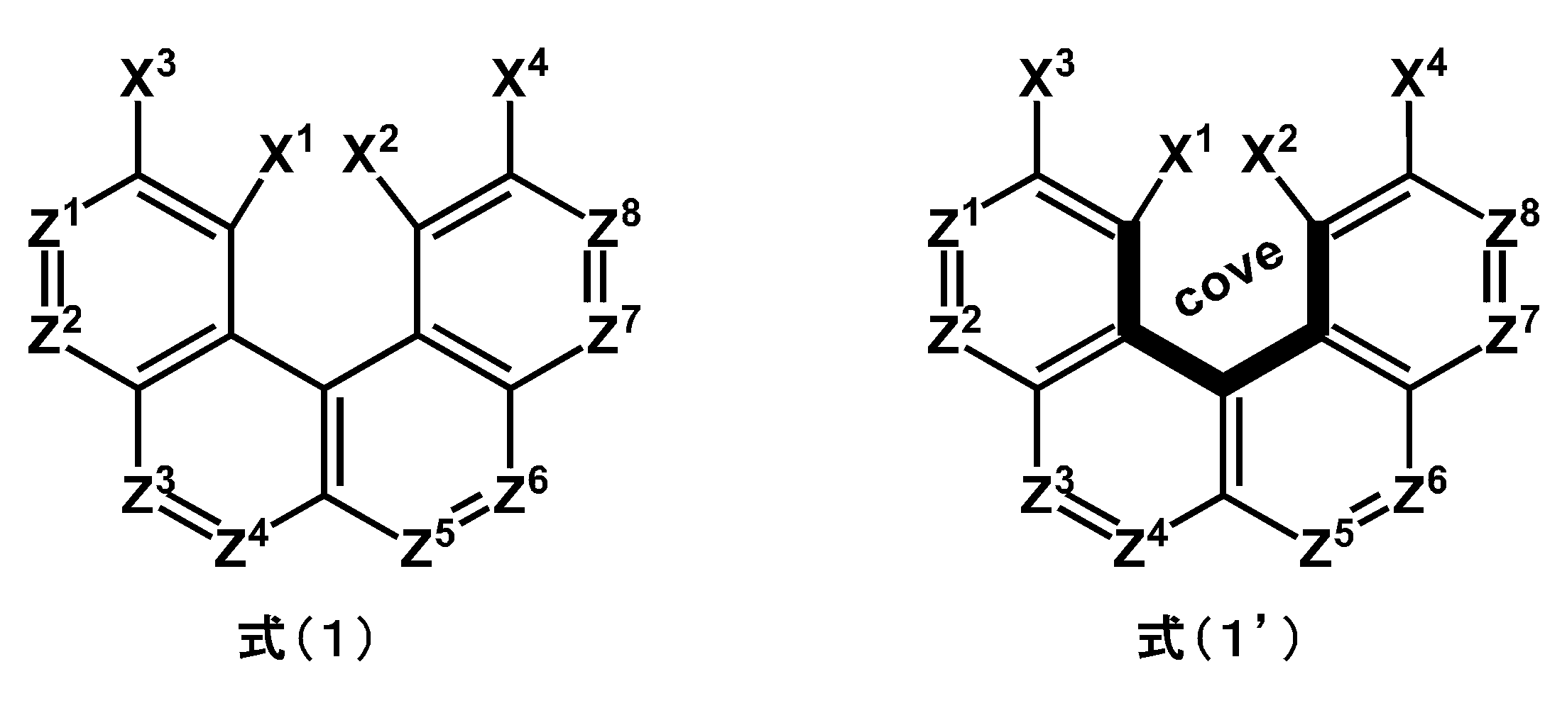
- a compound having a skeleton having a cove region in its molecular structure, and the skeleton being optionally substituted provided that the compound is dibenzo[g,p]chrysene
- a photoelectric conversion device material for an imaging device which does not contain
- a material for a photoelectric conversion element for an imaging device in which the skeleton is represented by the following formula (1).
- X 1 to X 4 each independently represent a hydrogen atom or a substituent; X 1 to X 4 are not bonded to each other to form a ring; a plurality of X 1 to X 4 may be the same or different; Z 1 to Z 8 each independently represent a nitrogen atom or a carbon atom which may have a substituent; at least 6 of Z 1 to Z 8 are carbon atoms which may have a substituent; multiple Z 1 to Z 8 may be the same or different; When any one of Z 1 to Z 8 is a carbon atom which may have a substituent, one or two substituents on any one of Z 1 to Z 8 adjacent to the carbon atom and may be combined to form a ring.
- the photoelectric conversion element material for an image pickup element according to the above aspect which is a transport material for an image pickup element photoelectric conversion element or a charge blocking material for an image pickup element photoelectric conversion element.
- the photoelectric conversion element material for an image pickup element according to the above aspect which is a hole transport material for an image pickup element photoelectric conversion element or an electron blocking material for an image pickup element photoelectric conversion element. be.
- a photoelectric conversion element for an image pickup device including the photoelectric conversion element material for an image pickup device according to the above aspect.
- a photoelectric conversion element material for an image pickup element for an image pickup element, a hole transport material for an image pickup element photoelectric conversion element, and an image pickup device that contribute to the production of a photoelectric conversion element for an image pickup device excellent in dark current and external quantum efficiency Electron blocking materials for photoelectric conversion devices for devices can be provided.
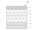
- FIG. 1 is a schematic cross-sectional view showing an example of a lamination structure of a photoelectric conversion element for an image pickup device containing a photoelectric conversion element material for an image pickup device according to one aspect of the present invention.
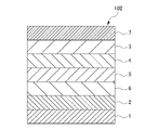
- FIG. 4 is a schematic cross-sectional view showing the lamination structure of Element Example A-1.
- FIG. 10 is a schematic cross-sectional view showing the lamination structure of Element Example B-1.
- One aspect of the present invention includes a compound that includes a skeleton having a cove region in its molecular structure, and that the skeleton may be substituted, provided that the compound is an unsubstituted dibenzo[g,p] It is a material for a photoelectric conversion element for an imaging device that does not contain chrysene.
- a Cove region is a name that indicates a specific molecular structure region in a polycyclic compound, and refers to a region disclosed in, for example, non-patent literature (Chemical Science, 2019, 10, 4025.). In addition, in this specification, a compound is also included in a "material.”
- the cove region refers to a curved region formed by combining four sides of each benzene ring in the [4] helicene skeleton in which four benzene rings are condensed.
- at least one of hydrogen atoms and carbon atoms in the above [4] helicene skeleton having a cove region may be substituted.
- the [4] helicene skeleton also includes a heterohelicene skeleton in which a part of the benzene ring is replaced with a hetero ring.
- the photoelectric conversion element material for an imaging device contains a heterohericene skeleton having a cove region
- at least one of a hydrogen atom, a carbon atom, an oxygen atom, a sulfur atom, and a nitrogen atom in the heterohericene skeleton is substituted.
- the substituent possessed by the skeleton is preferably a charge-transporting substituent. The details of the charge-transporting substituent are described later, and in this embodiment, the specific substituent described later can be used as it is.
- the [5] helicene skeleton in which five benzene rings are condensed or the [6] helicene skeleton in which six benzene rings are condensed can also be considered to partially include the Cove region. , these are called fjord areas and do not correspond to cove areas.
- the Cove region in the present invention refers to the region possessed by the compound represented by formula (1), more specifically, the region indicated by the thick line in formula (1'). That is, one embodiment of the present invention includes a compound containing a skeleton represented by formula (1), wherein the skeleton may be substituted, provided that the compound is an unsubstituted dibenzo[g,p]chrysene It is preferably a photoelectric conversion device material for an image pickup device that does not contain any.
- X 1 to X 4 each independently represent a hydrogen atom or a substituent; X 1 to X 4 are not bonded to each other to form a ring; a plurality of X 1 to X 4 may be the same or different; Z 1 to Z 8 each independently represent a nitrogen atom or a carbon atom which may have a substituent; at least 6 of Z 1 to Z 8 are carbon atoms which may have a substituent; multiple Z 1 to Z 8 may be the same or different; When any one of Z 1 to Z 8 is a carbon atom which may have a substituent, one or two substituents on any one of Z 1 to Z 8 adjacent to the carbon atom and may be combined to form a ring.
- ⁇ About X 1 to X 4 > X 1 to X 4 each independently represent a hydrogen atom or a substituent. X 1 to X 4 do not form a ring with each other and have the above-mentioned cove region in the molecular structure by not forming a ring. Both X 1 and X 2 are preferably hydrogen atoms from the viewpoint of producing a photoelectric conversion element material for an image pickup element with good yield. ⁇ Regarding Z 1 to Z 8 > Z 1 to Z 8 each independently represent a nitrogen atom or an optionally substituted carbon atom.
- Z 1 to Z 8 at least 6 are preferably carbon atoms which may have substituent(s), and at least 7 are more preferably carbon atoms which may have substituent(s). , are all preferably carbon atoms which may have a substituent.
- Z 3 and Z 4 are carbon atoms which may have a substituent, and the substituents of Z 3 and Z 4 are preferably bonded together to form a ring.
- the photoelectric conversion device material for an imaging device which is one aspect of the present invention, preferably contains a compound represented by any one of formulas (2A) to (5B) below.
- A represents a charge-transporting substituent
- Ar 2 is an optionally substituted C6-30 monocyclic, linked or condensed aromatic hydrocarbon group, optionally substituted C3-36 monocyclic , a linked or condensed heteroaromatic group, and a linear or branched alkyl group having 1 to 18 carbon atoms
- R 1 and R 2 are each independently hydrogen atom; deuterium atom; optionally substituted monocyclic, linked or condensed aromatic hydrocarbon group having 6 to 30 carbon atoms; optionally substituted monocyclic, linked or condensed heteroaromatic group having 3 to 36 carbon atoms; a linear or branched alkyl group having 1 to 18 carbon atoms; or represents a linear or branched alkoxy group having 1 to 18 carbon atoms; R 1 and R 2 may combine with each other to form a ring.
- k represents an integer from 1 to 4;
- a plurality of A may be the same or different.
- a charge-transporting substituent is a substituent having a function of transporting charge.
- a charge is a hole, an electron, or both.
- Examples of the charge-transporting substituent include the following substituents (a-1) to (a-16).
- (a-1) a deuterium atom, (a-2) fluorine atom, chlorine atom, bromine atom, iodine atom, (a-3) a trifluoromethyl group,
- (a-4) a pentafluoroethyl group, (a-5) a cyano group, (a-6) a nitro group, (a-7) a hydroxyl group, (a-8) a thiol group, (a-9) an optionally substituted monocyclic, linked or condensed aromatic hydrocarbon group having 6 to 30 carbon atoms,
- (a-10) an optionally substituted monocyclic, linked or condensed heteroaromatic group having 3 to 36 carbon atoms,
- R 100 to R 300 are each independently (r-1) a hydrogen atom, (r-2) a deuterium atom, (r-3) an optionally substituted monocyclic, linked or condensed aromatic hydrocarbon group having 6 to 30 carbon atoms, (r-4) an optionally substituted monocyclic, linked or condensed heteroaromatic group having 3 to 36 carbon atoms, or (r-5) represents a linear or branched alkyl group having 1 to 18 carbon atoms; L are each independently a phenylene group optionally substituted with a methyl group or a phenyl group; a naphthylene group optionally substituted with a methyl group or a phenyl group; a biphenylene group optionally substituted with a methyl group or a phenyl group, or representing a single bond; n represents 1 or 2, if L is a single bond, n is 1; if L is not a single bond, n is 1 or 2; When n is
- the monocyclic, linked or condensed aromatic hydrocarbon group having 6 to 30 carbon atoms which is (a-9), includes, for example, a phenyl group, a biphenylyl group, a terphenylyl group, a naphthyl group, a fluorenyl group and an anthryl group. , phenanthryl group, benzofluorenyl group, triphenylenyl group, spirobifluorenyl group, diphenylfluorenyl group, dibenzo[g,p]chrysenyl group and the like.
- the monocyclic, linked or condensed aromatic hydrocarbon group having 6 to 30 carbon atoms is preferably a monocyclic, linked or condensed aromatic hydrocarbon group having 6 to 18 carbon atoms.
- the aromatic hydrocarbon group of (a-9) has a substituent
- the substituent is each independently a fluorine atom, a chlorine atom, a bromine atom, an iodine atom, a cyano group, a nitro group, and a hydroxyl group.
- a linear or branched alkyl group having 1 to 18 carbon atoms, a linear or branched alkoxy group having 1 to 18 carbon atoms, or a trifluoromethylsulfonyloxy group is preferable.
- the phosphine oxide group includes an unsubstituted phosphine oxide group and a phosphine oxide group having a substituent.
- a phosphine oxide group having a substituent is preferred.
- the phosphine oxide group having a substituent is preferably a monocyclic, linked or condensed aromatic hydrocarbon group having 6 to 18 carbon atoms, or a phosphine oxide group having a condensed heteroaromatic group. Specific examples include groups substituted with two aryl groups such as diphenylphosphine oxide.
- Silyl groups include unsubstituted silyl groups and substituted silyl groups.
- a silyl group having a substituent is preferred.
- the silyl group having a substituent is preferably a monocyclic, linked or condensed aromatic hydrocarbon group having 6 to 18 carbon atoms, or a silyl group having a condensed heteroaromatic group. Specific examples thereof include groups substituted with three aryl groups such as a triphenylsilyl group.
- Examples of the boronyl group optionally having a saturated hydrocarbon group having 2 to 10 carbon atoms include a dihydroxyboryl group (—B(OH) 2 ), 4,4,5,5-tetramethyl-[1, 3,2]-dioxaborolanyl group, 5,5-dimethyl-[1,3,2]-dioxaborinane group and the like.
- Linear or branched alkyl groups having 1 to 18 carbon atoms include, for example, methyl group, ethyl group, n-propyl group, i-propyl group, n-butyl group, sec-butyl group, tert-butyl group, pentyl group, n-hexyl group, cyclohexyl group, octyl group, decyl group, dodecyl group, octadecyl group and the like.
- Linear or branched alkoxy groups having 1 to 18 carbon atoms include, for example, methoxy group, ethoxy group, n-propoxy group, i-propoxy group, n-butoxy group, sec-butoxy group, tert-butoxy group, pentyl oxy group, n-hexyloxy group, cyclohexyloxy group, octyloxy group, decyloxy group, dodecyloxy group, octadecyloxy group and the like.
- the monocyclic, linked or condensed heteroaromatic group having 3 to 36 carbon atoms which is (a-10), contains at least one atom selected from the group consisting of an oxygen atom, a nitrogen atom, and a sulfur atom. It is a monocyclic, linked or condensed heteroaromatic group having 3 to 36 carbon atoms contained on an aromatic ring.
- heteroaromatic group examples include pyrrolyl group, thienyl group, furyl group, imidazolyl group, pyrazolyl group, thiazolyl group, isothiazolyl group, oxazolyl group, isoxazolyl group, pyridyl group, phenylpyridyl group, pyridylphenyl group and pyrimidyl group.
- pyrazyl group 1,3,5-triazyl group, 1,3,5-triazylphenyl group, 1,3,5-triazylbiphenylyl group, 4,6-diphenyl-1,3,5-triazyl group , indolyl group, benzothienyl group, benzofuranyl group, benzimidazolyl group, indazolyl group, benzothiazolyl group, benzoisothiazolyl group, 2,1,3-benzothiadiazolyl group, benzoxazolyl group, benzoisoxazolyl group , 2,1,3-benzoxadiazolyl group, quinolyl group, isoquinolyl group, quinoxalyl group, quinazolyl group, carbazolyl group, 9-phenylcarbazolyl group, 9-(4-biphenylyl)carbazolyl group, dibenzothienyl group, dibenzofuranyl group, phenoxazin
- the substituent is each independently a cyano group, a fluorine atom, a trifluoromethyl group, or a linear or branched chain having 1 to 18 carbon atoms. is preferably an alkyl group of , a linear or branched alkoxy group having 1 to 18 carbon atoms, or a trifluoromethylsulfonyloxy group.
- linear or branched alkyl group having 1 to 18 carbon atoms examples include the same linear or branched alkyl groups having 1 to 18 carbon atoms exemplified in (a-9) above.
- straight or branched alkoxy groups having 1 to 18 carbon atoms examples include the same straight or branched alkoxy groups having 1 to 18 carbon atoms exemplified in (a-9) above.
- the phosphine oxide group of (a-11) includes an unsubstituted phosphine oxide group and a phosphine oxide group having a substituent.
- a phosphine oxide group having a substituent is preferred.
- Examples of the substituted phosphine oxide group include the same phosphine oxide groups exemplified in (a-9) above.
- silyl group (a-12) examples include an unsubstituted silyl group and a silyl group having a substituent.
- a silyl group having a substituent is preferred.
- Silyl groups having substituents include, for example, the same silyl groups as exemplified in (a-9) above.
- a boronyl group optionally having a saturated hydrocarbon group having 2 to 10 carbon atoms or a boronyl group optionally having a saturated hydrocarbon group having 2 to 10 carbon atoms examples include the same boronyl groups as exemplified in (a-9) above.
- the linear or branched alkoxy group having 1 to 18 carbon atoms which is (a-15), includes, for example, the linear or branched alkoxy group having 1 to 18 carbon atoms exemplified in (a-9) above. The same can be mentioned.
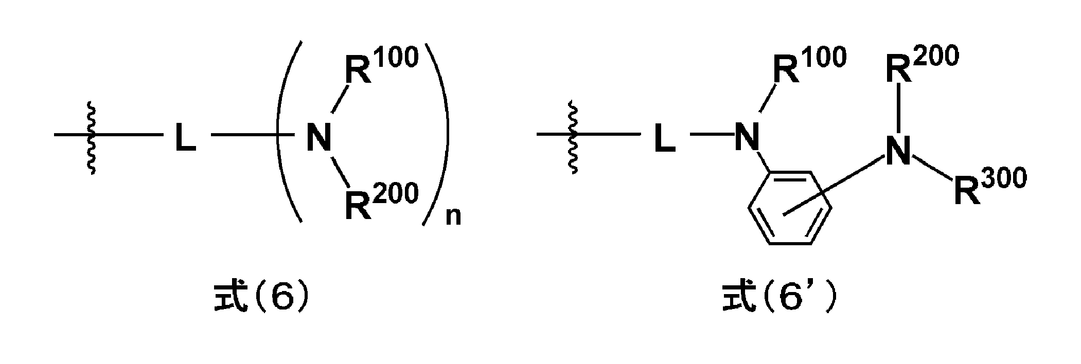
- (a-17) is a group represented by formulas (6) and (6′), and as described above, the charge-transporting group is a group represented by formula (6) or (6′) above. There may be.
- formulas (6) and (6') the definitions of L, R 100 to R 300 and n are as follows.
- R 100 to R 300 each independently have (r-1) a hydrogen atom, (r-2) a deuterium atom, and (r-3) a substituent a monocyclic, linked or condensed aromatic hydrocarbon group having 6 to 30 carbon atoms which may be substituted; Alternatively, it represents a condensed heteroaromatic group, or (r-5) a linear or branched alkyl group having 1 to 18 carbon atoms.
- R 100 to R 300 may be substituted with one substituent or may be substituted with two or more substituents.
- the definition of the monocyclic, linked or condensed aromatic hydrocarbon group having 6 to 30 carbon atoms which is the above (r-3), is as described in the above (a-9) except for the definitions of the substituents thereof. It is the same as the definition of a monocyclic, linked or condensed aromatic hydrocarbon group having 6 to 30 carbon atoms.
- the substituent may be a deuterium atom, a fluorine atom, a linear or branched alkyl group having 1 to 18 carbon atoms, or 18 linear or branched alkoxy group, 9-carbazolyl group, dibenzothienyl group, dibenzofuranyl group, N,N-diphenylamino group, or N,N-bis(4-biphenylyl)-amino group is preferred.
- the linear or branched alkyl group having 1 to 18 carbon atoms is the same as the linear alkyl group having 1 to 18 carbon atoms exemplified in (a-9) above.
- Examples of the linear or branched alkoxy group having 1 to 18 carbon atoms include the same linear or branched alkoxy groups having 1 to 18 carbon atoms exemplified in (a-9) above.
- the definition of the monocyclic, linked or condensed heteroaromatic group having 3 to 36 carbon atoms which is the above (r-4), is exemplified in (a-10) above, except for the definitions of the substituents.
- Examples thereof include the same monocyclic, linked or condensed heteroaromatic groups having 3 to 36 carbon atoms. More preferably, it is a monocyclic, linked or condensed heteroaromatic group having 3 to 20 carbon atoms.
- the substituent may be a deuterium atom, a fluorine atom, a linear or branched alkyl group having 1 to 18 carbon atoms, or 1 to 18 carbon atoms.
- These substituents have, for example, the same definition as the aforementioned substituent (r-3).
- L is a phenylene group optionally substituted by a methyl group or a phenyl group; a naphthylene group optionally substituted by a methyl group or a phenyl group; a methyl group or a phenyl group a biphenylene group optionally substituted with; or represents a single bond.
- phenylene group examples include 1,2-phenylene group, 1,3-phenylene group, and 1,4-phenylene group.
- naphthylene group examples include naphthalene-1,2-diyl group, naphthalene-1,4-diyl group, naphthalene-1,8-diyl group, and naphthalene-2,3-diyl group.
- biphenylene group examples include biphenyl-4,4'-diyl group, biphenyl-4,3'-diyl group, biphenyl-4,2'-diyl group, biphenyl-3,3'-diyl group, biphenyl- 3,2'-diyl group, biphenyl-2,2'-diyl group and the like.
- n represents an integer of 1 or 2.
- n is an integer of 1; n is an integer of 1 or 2 when L is not a single bond.
- R 100 and R 200 there are two each of R 100 and R 200 , which may be the same or different.
- R 1 and R 2 are (b-3) an aromatic hydrocarbon group having a substituent or (b-4) a heteroaromatic group having a substituent
- the substituents are each independently , a deuterium atom, a fluorine atom, a linear or branched alkyl group having 1 to 18 carbon atoms, or a linear or branched alkoxy group having 1 to 18 carbon atoms.
- Specific examples of the linear or branched alkyl group having 1 to 18 carbon atoms and the linear or branched alkoxy group having 1 to 18 carbon atoms are not particularly limited, but are described above (a- Examples are the same as those exemplified in 9).
- R 1 and R 2 may combine with each other to form a ring.
- R 1 and R 2 are phenyl, they can be joined together to form a fluorene ring.
- (b-4) an optionally substituted monocyclic, linked or condensed heteroaromatic group having 3 to 36 carbon atoms
- R 1 and R 2 of formulas (4A) to (4C) examples include, but are not particularly limited to, pyridyl groups and the like.
- R 1 and R 2 are each independently from the viewpoint of availability of raw materials, a phenyl group, a biphenylyl group, a pyridyl group, a pyrimidyl group, or a group in which these groups are substituted with a methyl group or a methoxy group; A methyl group, an n-butyl group, or an n-hexyl group is preferred.
- R 1 and R 2 are each independently A phenyl group, or a group substituted with a methyl group or a methoxy group; or a methyl group is more preferable.
- k is each independently an integer of 0 or more and 4 or less.
- k is 2 or more, there are a plurality of Ars, and the plurality of Ars may be the same or different.
- k is preferably 3 or less, more preferably 2 or less.
- the molecular weight becomes smaller than that of compounds with k of 4 or more. As a result, the sublimation temperature of the compound is lowered, and the heat resistance stability during sublimation is improved, which is preferable.
- A examples include groups (1) to (24) shown below.
- N,N-diphenylamino group N,N-bis(4-biphenylyl)-amino group, N,N-bis(3-biphenylyl)-amino group, N-phenyl-4-biphenylamino group, N-phenyl-3-biphenylamino group, N-(4-biphenyl)-4-p-terphenylamino group, N-[4-(carbazol-9-yl)phenyl]-4-biphenylamino group, N 3 -[1,1′-biphenyl]-4-yl-N 1 ,N 1 -diphenyl-1,3-benzenediamino group, 4-triphenylamino group, 3-triphenylamino group, 4-(4 ',4''-diphenyl)triphenylamino group, 3-(4',4'-diphenyl)triphenylamino group, N 1 ,N 1 ,
- A is each independently a phenyl group, a biphenylyl group, a pyridylphenyl group, a terphenylyl group, a naphthyl group, phenanthryl group, pyrenyl group, 9,9-spirobi[9H-fluorenyl] group, triphenylenyl group, dibenzothienyl group, dibenzofuranyl group, pyridyl group, pyrimidyl group, or these groups are cyano group, nitro group, hydroxyl a group substituted with a group, a thiol group, a fluorine atom, a chlorine atom, a chlorine atom, a bromine atom, an iodine atom, a methyl group, a methoxy group, or a trifluoromethylsulfonyloxy group; fluorenyl group, benzo
- Tables B-1 to B-7 have the skeletons and substitution positions of (3Aa) to (4Cd) shown in Tables A-1 to A-3, and the substituent A at the substitution position is Compounds (N-1) to (N-275), which are groups shown in B-1 to B-7, are shown.
- Preferred specific examples of the material for photoelectric conversion elements for imaging elements represented by Formula (1) include the compounds shown below.
- Preferred specific examples of the material for photoelectric conversion elements for imaging elements represented by formula (1) also include the compounds shown below.
- the photoelectric conversion device material for image pickup device can be synthesized by a known method.
- JP-A-2018-193371, JP-A-2019-34939, JP-A-2019-116472, JP-A-2019-34933, JP-A-2020-33332, JP-A-2020-15691 It can be synthesized by known methods disclosed in JP-A-2011-6397, Japanese Patent No. 4968333, US2019/0198781, and International Publication No. 2017/109722.
- a known material can be used as the photoelectric conversion element material for an imaging element according to one aspect of the present invention.
- the material for photoelectric conversion elements for imaging devices can be used, for example, as a transport material for photoelectric conversion devices for imaging devices and a charge blocking material for photoelectric conversion devices for imaging devices.
- a photoelectric conversion device material for an imaging device includes a compound containing a skeleton represented by the above formula (1).
- the transport material for a photoelectric conversion device for an imaging device and the charge blocking material for a photoelectric conversion device for an imaging device according to one aspect of the present invention contain a compound containing a skeleton represented by Formula (1).
- the photoelectric conversion element material for an image pickup element, the transport material for an image pickup element photoelectric conversion element, and the charge blocking material for an image pickup element photoelectric conversion element that contain a compound containing a skeleton represented by formula (1) are dark current and external This contributes to the production of a photoelectric conversion device material for an imaging device having excellent quantum efficiency characteristics.
- the photoelectric conversion device material for an image pickup device according to one aspect of the present invention or the photoelectric conversion device material for an image pickup device represented by formula (1) has a molecular weight of 1500 or less from the viewpoint of heat resistance stability during sublimation. is preferred, and 1000 or less is more preferred.
- the HOMO level of the photoelectric conversion device material for an image pickup device according to one aspect of the present invention or the material for a photoelectric conversion device for an image pickup device represented by formula (1) is not particularly limited. From the point of view of suitability, the HOMO is preferably 5.0-6.5 eV. This HOMO value is a value obtained from measurement with an atmospheric photoelectron yield spectrometer for the deposited film.
- the bandgap of the photoelectric conversion element material for an image pickup element according to one aspect of the present invention or the material for an image pickup element photoelectric conversion element represented by formula (1) is not particularly limited, it is suitable for the photoelectric conversion element for an image pickup element.
- the bandgap is preferably 2.5 to 4.0 eV. This bandgap is a value obtained from the wavelength edge of the absorption spectrum of the deposited film.
- the LUMO level of the photoelectric conversion element material for an image pickup element according to one aspect of the present invention or the material for an image pickup element photoelectric conversion element represented by formula (1) is not particularly limited, From the point of view of suitability, a LUMO of 2.0 to 3.5 eV is preferred. This LUMO value is a value obtained from the HOMO value and bandgap.
- the glass transition temperature of the photoelectric conversion device material for an image pickup device according to one aspect of the present invention or the material for a photoelectric conversion device for an image pickup device represented by formula (1) is not particularly limited. From the viewpoint of compatibility, the glass transition temperature is preferably 100° C. or higher, more preferably 110° C. or higher, and particularly preferably 130° C. or higher. This glass transition temperature is a value obtained from differential scanning calorimetry.
- the photoelectric conversion element material for an image pickup element according to one aspect of the present invention or the photoelectric conversion element material for an image pickup element represented by Formula (1) preferably forms an amorphous layer as a vapor-deposited film of the material. If the deposited film is a crystalline layer, the interface with the adjacent layer will not be uniform, resulting in device defects.
- the method for confirming whether the deposited film is an amorphous layer is not particularly limited, but it can be confirmed by visually checking for the presence or absence of crystallization, or by not observing a sharp diffraction peak by XRD measurement of the deposited film.
- One aspect of the present invention is to find out that a compound having a cove region is promising as a photoelectric conversion element material for an imaging device. It is known that in the skeleton represented by formula ( 1 ), the presence of the Cove region causes twisting in the conjugated system in order to eliminate the steric repulsion between X1 and X2. Due to this effect, the material for a photoelectric conversion element for an imaging element, which is one embodiment of the present invention, has improved amorphous stability in a vapor-deposited film, compared to a conventional material having a planar polycyclic compound as a core. Excellent.
- the photoelectric conversion element material for an imaging element which is one embodiment of the present invention, can be expected to have an effect of stacking in a columnar manner in which mother nuclei overlap each other due to the twist of the conjugated system.
- the photoelectric conversion device material for an imaging device which is one aspect of the present invention, uses a twisted polycyclic compound having a cove region as a core, so that the amorphous film of the vapor deposition film is stable and even in the vapor deposition film. It is surmised that the excellent dark current in the photoelectric conversion element for the image pickup device was achieved by arranging the scaffolds with some regularity and securing a good charge transport path.
- one aspect of the present invention is that the skeleton is substituted, thereby adjusting the HOMO level, improving the glass transition temperature, improving the amorphous property, improving the charge transport property, improving the blocking property against reverse charge, and the like.
- the material for a photoelectric conversion element for an imaging device which is one embodiment of the present invention
- the hole is well transported and the charge is reversed.
- the effect of blocking electrons can be expected. By blocking the reverse charge, it is possible to suppress the dark current in the photoelectric conversion element for an imaging device.
- a photoelectric conversion element for an image pickup device includes the photoelectric conversion element material for an image pickup device according to the embodiment of the present invention.
- the configuration of the photoelectric conversion element for the imaging device is not particularly limited, for example, the following configurations (i) to (vi) can be mentioned.
- FIG. 1 is a schematic cross-sectional view showing an example of a lamination structure of a photoelectric conversion element for an image pickup device containing a photoelectric conversion element material for an image pickup device according to one aspect of the present invention.
- a photoelectric conversion element 100 for an imaging device includes a substrate 1, a lower electrode 2, a buffer layer 3, a hole transport layer 4, a photoelectric conversion layer 5, an electron transport layer 6, and an upper electrode 7 in this order.
- the hole-transporting layer 4 and the electron-transporting layer 6 may be the names of an electron-blocking layer and a hole-blocking layer, respectively. However, some of these layers may be omitted, or conversely, other layers may be added.
- the photoelectric conversion element for an imaging device shown in FIG. 1 In the photoelectric conversion element for an imaging device shown in FIG. 1, light enters from below the transparent lower electrode 2 . Further, in the photoelectric conversion element for an imaging device, the voltage is applied such that, of the charges (holes and electrons) generated in the photoelectric conversion layer 5, the holes are moved to the lower electrode 2 and the electrons are moved to the upper electrode 7. applied. That is, the lower electrode 2 is used as a hole collecting electrode, and the upper electrode 7 is used as an electron collecting electrode.
- the photoelectric conversion element for an imaging device contains a photoelectric conversion element material for one or more layers selected from the group consisting of a photoelectric conversion layer and a layer between the photoelectric conversion layer and a lower electrode. Therefore, in the configuration example shown in FIG. 1 , the photoelectric conversion element 100 for an image pickup element includes a photoelectric conversion element material for an image pickup element in at least one layer selected from the group consisting of the photoelectric conversion layer 5 and the hole transport layer 4 . In particular, it is preferable that the hole transport layer 4 contains a photoelectric conversion element material for an imaging element.
- the photoelectric conversion element material for an image pickup device may be contained in a plurality of layers provided in the photoelectric conversion element for an image pickup device, and an electron blocking layer is provided between the photoelectric conversion layer and the hole transport layer. If so, the electron blocking layer may contain a photoelectric conversion element material for an imaging element.
- a photoelectric conversion element 100 for an image pickup device in which the hole transport layer 4 contains a material for a photoelectric conversion device for an image pickup device will be described below.
- the substrate is not particularly limited, and examples thereof include a glass plate, a quartz plate, a plastic plate and the like. Further, in the case of a configuration in which light is incident from the substrate 1 side, the substrate 1 is transparent to the wavelength of light.
- a lower electrode 2 is provided on the substrate 1 .
- the lower electrode is made of a transparent material that allows the light to pass through or substantially pass through.
- the transparent material used for the lower electrode 2 is not particularly limited, but examples include indium-tin oxide (ITO), indium-zinc oxide (IZO), tin oxide. , aluminum-doped tin oxide, magnesium-indium oxide, nickel-tungsten oxide, other metal oxides, metal nitrides such as gallium nitride, metal selenides such as zinc selenide, and metal sulfides such as zinc sulfide things, etc.
- ITO indium-tin oxide
- IZO indium-zinc oxide
- tin oxide aluminum-doped tin oxide, magnesium-indium oxide, nickel-tungsten oxide, other metal oxides, metal nitrides such as gallium nitride, metal selenides such as zinc selenide, and metal sulfides such as zinc sulfide things, etc.
- the transmission characteristics of the lower electrode are not important. Accordingly, examples of materials used for the lower electrode in this case include iridium, molybdenum, palladium, and platinum.
- a buffer layer 3 is provided between the lower electrode 2 and a hole transport layer 4 which will be described later.
- the buffer layer 3 also plays a role of efficiently accepting holes from the hole transport layer (electron blocking layer) 4 by adjusting the work function, and is also called a hole injection layer or a work function adjustment layer.
- Specific examples of the conventionally known buffer layer 3 include naphthalene-1,4,5,8-tetracarboxylic dianhydride (NTCDA), 2,3,6,7,10,11-hexacyano-1,4, 5,8,9,12-hexaazatriphenylene (HATCN) and the like.
- a hole transport layer (also called an electron blocking layer) 4 is provided between the buffer layer 3 and the photoelectric conversion layer 5 .
- the hole transport layer 4 serves to transport holes generated in the photoelectric conversion layer 5 from the photoelectric conversion layer 5 to the lower electrode 2 side, and to prevent electrons generated in the photoelectric conversion layer 5 from moving toward the lower electrode 2 side. and a blocking role.
- the hole transport layer 4 preferably contains a photoelectric conversion element material for an imaging element.
- the hole-transporting layer 4 may have a single-layer structure composed of one or more materials, or may have a laminated structure composed of multiple layers having the same composition or different compositions. That is, a material having both a hole-transporting property and an electron-blocking property may be formed in a single-layer structure as the hole-transporting layer, or a material specialized for hole-transporting property may be formed as the hole-transporting layer, A material specialized for electron blocking properties may be formed as an electron blocking layer on the hole transport layer to form a laminated structure.
- the hole-transporting layer 4 may further contain a conventionally known hole-transporting material in addition to the photoelectric conversion element material for an imaging element.
- Conventionally known hole transport materials include aromatic tertiary amine compounds, naphthalene compounds, anthracene compounds, tetracene compounds, pentacene compounds, phenanthrene compounds, pyrene compounds, perylene compounds, fluorene compounds, carbazole compounds, indole compounds, and pyrrole compounds.
- fluorene compounds preferred are fluorene compounds, naphthodithiophene compounds, naphthothienothiophene compounds, benzodifuran compounds, benzothiophene compounds, naphthobisbenzothiophene compounds, chrysenodithiophene compounds, benzothienobenzothiophene compounds, indolocarbazole compounds, and the like.
- Fluorene compounds, chrysenodithiophene compounds, benzothienobenzothiophene compounds, and indolocarbazole compounds are particularly preferred.
- hole transport materials include 9,9′-(9,9′-spirobi[9H-fluorene]-2,7′-diyl)bis[9H-carbazole], 2,7-diphenyl [1] benzothieno[3,2-b] [1] benzothiophene (DiPh-BTBT), benzo[1,2-b:3,4-b′:5,6-b′′]trifurane compound, benzo[ 1,2-b:3,4-b′:5,6-b′′]trithiophene compound, naphtho[1,2-b:5,6-b′]dithiophene, naphtho[2,3-b] naphtho[2′,3′:4,5]thieno[2,3-d]thiophene, benzo[1,2-b:4,5-b′]difuran, benzo[1,2-b:4,5 -b']dithiophene, benzo[1,2-b:4,5-b']bis[1]benzo
- a photoelectric conversion layer 5 is provided between the hole transport layer 4 and an electron transport layer 6 which will be described later.
- Examples of materials for the photoelectric conversion layer 5 include materials having a photoelectric conversion function.
- the photoelectric conversion layer 5 may have a single layer structure composed of one or more materials, or may have a laminated structure composed of a plurality of layers having the same composition or different compositions.
- Examples of the material used for the photoelectric conversion layer 5 having a single-layer structure made of one material include (1) coumarin and its derivatives, quinacridone and its derivatives, phthalocyanine and its derivatives, and the like.
- Examples of materials used for the photoelectric conversion layer 5, which has a single-layer structure composed of two materials include (i) coumarin and its derivatives, quinacridone and its derivatives, phthalocyanine and its derivatives, and (ii) fullerene and Combinations with derivatives thereof are also included.
- the photoelectric conversion layer 5 made of these materials may be formed by vapor deposition in a state in which powders are mixed in advance, or may be formed by co-evaporation in an arbitrary ratio.
- the materials used for the photoelectric conversion layer 5, which has a single-layer structure composed of three materials, include (i) coumarin and its derivatives, quinacridone and its derivatives, phthalocyanine and its derivatives, (ii) fullerene and its derivatives, and (iii) combinations with hole-transporting materials;
- the photoelectric conversion layer 5 made of these materials may be formed by vapor deposition in a state in which powders are mixed in advance, or may be formed by co-evaporation in an arbitrary ratio.
- coumarin derivatives include coumarin 6 and coumarin 30.
- quinacridone derivatives include N,N-dimethylquinacridone.
- phthalocyanine derivatives include boron-subphthalocyanine chloride and boron-subnaphthalocyanine chloride (SubNC).
- fullerene and derivatives thereof include [60]fullerene, [70]fullerene, and [6,6]-phenyl-C61-methylbutyrate ([60]PCBM).
- Preferred compounds and specific examples of the hole-transporting material are the same as those described for the hole-transporting layer 4 above.
- the material having a photoelectric conversion function is not limited to being contained only in the photoelectric conversion layer.
- the material having a photoelectric conversion function may be contained in a layer adjacent to the photoelectric conversion layer 5 (the hole transport layer 4 or the electron transport layer 6).
- An electron transport layer (also called a hole blocking layer) 6 is provided between the photoelectric conversion layer 5 and an upper electrode 7 to be described later.
- the electron transport layer 6 has a role of transporting electrons generated in the photoelectric conversion layer 5 to the upper electrode 7 side and a role of blocking the movement of holes generated in the photoelectric conversion layer 5 to the upper electrode 7 side. .
- the electron transport layer 6 can contain a conventionally known electron transport material.
- Conventionally known electron transport materials include, for example, bis(8-hydroxyquinolinato)manganese, tris(8-hydroxyquinolinato)aluminum, tris(2-methyl-8-hydroxyquinolinato)aluminum, BCP ( 2,9-dimethyl-4,7-diphenyl-1,10-phenanthroline), Bphen (4,7-diphenyl-1,10-phenanthroline), BAlq (bis(2-methyl-8-quinolinolate)-4-( phenylphenolate)aluminum), 4,6-bis(3,5-di(pyridin-4-yl)phenyl)-2-methylpyrimidine, N,N'-diphenyl-1,4,5,8-naphthalenetetra carboxylic acid diimide, N,N'-di(4-pyridyl)-1,4,5,8-naphthalenetetracarboxylic acid diimide, and the like.
- the electron-transporting layer 6 may have a single-layer structure composed of one or more materials, or may have a laminated structure composed of multiple layers having the same composition or different compositions.
- An upper electrode 7 is provided on the electron transport layer 6 .
- Materials for the upper electrode 7 include sodium, sodium-potassium alloy, magnesium, lithium, magnesium/copper mixture, silver, magnesium/silver mixture, magnesium/aluminum mixture, magnesium/indium mixture, aluminum/aluminum oxide (Al 2 O 3 ) mixtures, indium, lithium/aluminum mixtures, rare earth metals, and the like.
- Each layer except for the lower electrode 2 and the upper electrode 7 described above is formed by applying the material of each layer (with a material such as a binder resin and a solvent as necessary) to, for example, a vacuum vapor deposition method, a spin coating method, a casting method, an LB method, or the like. (Langmuir-Blodgett method) method or the like to form a thin film.
- the thickness of each layer thus formed is not particularly limited and can be appropriately selected depending on the situation, but is usually in the range of 5 nm or more and 5 ⁇ m or less.
- the lower electrode 2 and the upper electrode 7 can be formed by thinning an electrode material by a method such as vapor deposition or sputtering.
- a pattern may be formed through a mask of a desired shape during vapor deposition or sputtering, or a pattern of a desired shape may be formed by photolithography after forming a thin film by vapor deposition, sputtering, or the like.
- the film thickness of the lower electrode 2 and the upper electrode 7 is preferably 1 ⁇ m or less, more preferably 10 nm or more and 200 nm or less.
- the materials constituting the lower electrode 2 and the upper electrode 7 may be exchanged as necessary, or the same material may be used (also called an inverse structure).
- the same material for example, when the lower electrode 2 is ITO, the upper electrode 7 is formed as an ITO layer by sputtering.
- the photoelectric conversion element for an imaging device is configured such that light passes through the upper electrode 7 and is incident on the photoelectric conversion layer 5 .
- the layers may be laminated in the reverse order of the above (v). For example, configurations shown in (I) to (IV) below can be given.
- the buffer layer serves to reduce damage to the organic film when the upper electrode is formed by sputtering.
- An imaging device including a photoelectric conversion device can be applied to, for example, imaging devices of digital cameras and digital video cameras, and imaging devices built into mobile phones and the like.
- FIG. 2 (Device Example A-1: Preparation of Photoelectric Conversion Device for Imaging Device Using Compound (2C-7))
- a photoelectric conversion element 101 for an imaging device having a laminated structure consisting of a substrate 1, a lower electrode 2, a hole transport layer 4, a photoelectric conversion layer 5, an electron transport layer 6, and an upper electrode 7 is produced, The dark current of the photoelectric conversion element was evaluated.
- substrate 1 and lower electrode 2 As a substrate having a lower electrode on its surface, a glass substrate with an ITO transparent electrode, in which an indium-tin oxide (ITO) film (thickness: 110 nm) with a width of 2 mm was patterned in stripes, was prepared. Then, after washing the substrate with isopropyl alcohol, the surface was treated by ozone ultraviolet washing.
- ITO indium-tin oxide
- each layer was vacuum-deposited on the surface-treated substrate after cleaning by a vacuum deposition method to laminate each layer.
- the glass substrate was introduced into a vacuum deposition tank, and the pressure was reduced to 7.0 ⁇ 10 ⁇ 5 Pa. Then, each layer was produced in the following order according to the film forming conditions of each layer.
- a photoelectric conversion layer 5 was produced by depositing N,N-dimethylquinacridone to a thickness of 100 nm at a rate of 0.30 nm/sec.
- Tris(8-hydroxyquinolinato)aluminum was deposited at a rate of 0.15 nm/second to a thickness of 30 nm to prepare an electron transport layer 6 .
- a photoelectric conversion element 101 for an image sensor having an area of 4 mm 2 as shown in FIG. 2 was produced.
- Each film thickness was measured with a stylus film thickness meter (DEKTAK, manufactured by Bruker).
- this device was sealed in a nitrogen atmosphere glove box with an oxygen and moisture concentration of 1 ppm or less. Sealing was performed by using a bisphenol F-type epoxy resin (manufactured by Nagase ChemteX Corporation) between the glass sealing cap and the film formation substrate (element).
- a bisphenol F-type epoxy resin manufactured by Nagase ChemteX Corporation
- Element Examples A-2 to A-3 Element Comparative Example A-1
- compounds (2C-25), (3Ja-186), 2,7-diphenyl[1]benzothieno[3,2-b, respectively were substituted for compound (2C-7) in that order.
- [1] A photoelectric conversion device for an imaging device was produced and evaluated in the same manner as in Device Example A-1, except that benzothiophene (DiPh-BTBT) was used. Table 1 shows the measurement results obtained.
- the photoelectric conversion element material for an imaging element according to one embodiment of the present invention can provide a dark current on the order of two or three digits lower than that of the comparative compound.
- a photoelectric conversion element 102 for an imaging device having a laminated structure consisting of a substrate 1, a lower electrode 2, an electron transport layer 6, a photoelectric conversion layer 5, a hole transport layer 4, a buffer layer 3, and an upper electrode 7. was produced, and the dark current and external quantum efficiency of the photoelectric conversion device were evaluated.
- An electron-transporting layer 6 was produced by depositing a 10 nm film of sublimation-purified compound 4,6-bis(3,5-di(pyridin-4-yl)phenyl)-2-methylpyrimidine at a rate of 0.10 nm/sec. .
- a photoelectric conversion layer 5 was produced by depositing N,N-dimethylquinacridone and C60 at a ratio of 4:1 (mass ratio) to a thickness of 120 nm. The deposition rate was 0.15 nm/sec.
- a hole transport layer 4 was prepared by forming a film of 10 nm from the sublimation-purified compound (2C-1) at a rate of 0.10 nm/sec.
- a photoelectric conversion element 102 for an image sensor having an area of 4 mm 2 as shown in FIG. 3 was produced.
- Each film thickness was measured with a stylus film thickness meter (DEKTAK, manufactured by Bruker).
- this device was sealed in a nitrogen atmosphere glove box with an oxygen and moisture concentration of 1 ppm or less. Sealing was performed by using a bisphenol F-type epoxy resin (manufactured by Nagase ChemteX Corporation) between the glass sealing cap and the film formation substrate (element).
- a bisphenol F-type epoxy resin manufactured by Nagase ChemteX Corporation
- the absolute value A current in the dark (dark current) and an external quantum efficiency were evaluated when a voltage of 2.5 V was applied as . Dark current measurements were evaluated using a Keithley Source Measure Unit 2636B. A solar cell spectral sensitivity measuring device (manufactured by Soma Kogaku Co., Ltd.) was used to measure the external quantum efficiency. The wavelength of the irradiation light was 560 nm, and the measurement was performed at an intensity of 50 ⁇ W/cm 2 . Table 2 shows the results.
- the photoelectric conversion element material for an imaging element according to one embodiment of the present invention can provide a higher external quantum efficiency than the comparative compound.
Landscapes
- Chemical & Material Sciences (AREA)
- Organic Chemistry (AREA)
- Physics & Mathematics (AREA)
- Spectroscopy & Molecular Physics (AREA)
- Engineering & Computer Science (AREA)
- Materials Engineering (AREA)
- Electroluminescent Light Sources (AREA)
- Light Receiving Elements (AREA)
- Solid State Image Pick-Up Elements (AREA)
Abstract
Description
ところで、特許文献3は、光電変換層と上部電極との間に無置換のジベンゾ[g,p]クリセンを結晶層として用いる記載がある。しかし、特許文献3ではジベンゾ[g,p]クリセンの分子構造上の特徴や、ジベンゾ[g,p]クリセンを含むアモルファス膜に関して一切言及していない。加えて、特許文献3に記載のジベンゾ[g,p]クリセンは、撮像素子用光電変換素子の性能を向上させる知見を何ら提供していない。
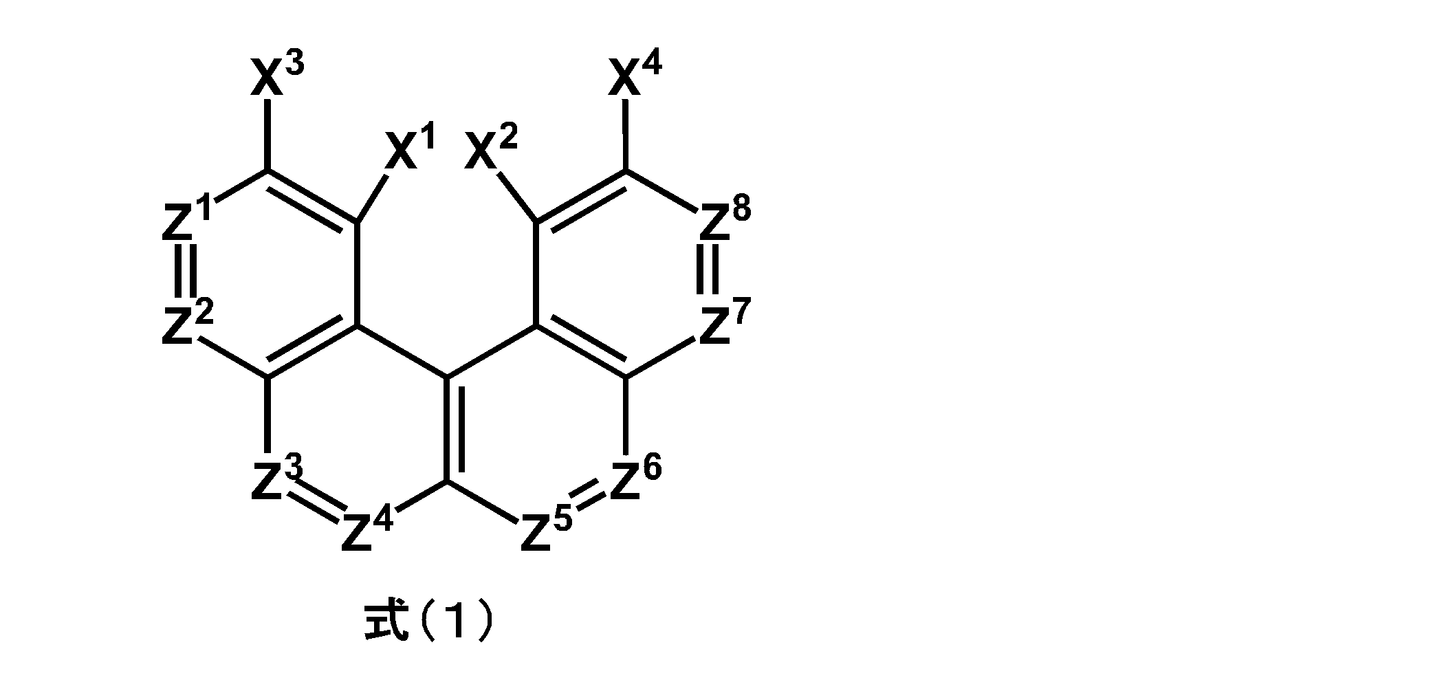
X1~X4は、それぞれ独立して、水素原子または置換基を表し;
X1~X4は、互いに結合して環を形成することはなく;
複数のX1~X4は、同一であっても異なっていてもよく;
Z1~Z8は、それぞれ独立して、窒素原子、または置換基を有していてもよい炭素原子を表し;
Z1~Z8の内、少なくとも6つは置換基を有していてもよい炭素原子であり;
複数のZ1~Z8は、同一であっても異なっていてもよく;
Z1~Z8のいずれかが、置換基を有していてもよい炭素原子の場合、該炭素原子に隣接する1つあるいは2つのZ1~Z8いずれかの炭素原子上の置換基と結合し、環を形成してもよい。
本発明の他の態様によれば、撮像素子用光電変換素子用正孔輸送材料または撮像素子用光電変換素子用電子ブロッキング材料である、上記態様に係る撮像素子用光電変換素子用材料が提供される。
本発明の他の態様によれば、上記態様に係る撮像素子用光電変換素子用材料を含む撮像素子用光電変換素子が提供される。
本発明の一態様は、分子構造中にコーブ(cove)領域を有する骨格を含み、該骨格が置換されていてもよい化合物を含み、ただし、該化合物として、無置換のジベンゾ[g,p]クリセンを含まない、撮像素子用光電変換素子用材料である。コーブ領域とは、多環式化合物における特定の分子構造領域を指す呼称であり、例えば、非特許文献(Chemical Science,2019,10,4025.)に開示された領域を指す。なお、本明細書において、「材料」には、化合物も包含される。
上記コーブ領域を有する骨格が置換された態様において、該骨格が有する置換基は、電荷輸送性置換基であることが好ましい。電荷輸送性置換基の詳細については、後述しており、本態様においても、後述した具体的な置換基をそのまま用いることができる。
なお、5個のベンゼン環が縮環した[5]ヘリセン骨格または6個のベンゼン環が縮環した[6]ヘリセン骨格にも、部分的にコーブ領域が含まれていると見ることもできるが、これらはフィヨルド(fjord)領域と呼称される領域であって、コーブ領域には該当しない。
X1~X4は、それぞれ独立して、水素原子または置換基を表し;
X1~X4は、互いに結合して環を形成することはなく;
複数のX1~X4は、同一であっても異なっていてもよく;
Z1~Z8は、それぞれ独立して、窒素原子、または置換基を有していてもよい炭素原子を表し;
Z1~Z8の内、少なくとも6つは置換基を有していてもよい炭素原子であり;
複数のZ1~Z8は、同一であっても異なっていてもよく;
Z1~Z8のいずれかが、置換基を有していてもよい炭素原子の場合、該炭素原子に隣接する1つあるいは2つのZ1~Z8いずれかの炭素原子上の置換基と結合し、環を形成してもよい。
<X1~X4について>
X1~X4は、それぞれ独立して、水素原子または置換基を表す。X1~X4は、互いに環を形成することはなく、環形成をしないことで上記コーブ領域を分子構造中に有する。撮像素子用光電変換素子用材料を収量良く製造する観点から、X1およびX2は、いずれも水素原子であることが好ましい。
<Z1~Z8について>
Z1~Z8は、それぞれ独立して、窒素原子、または置換基を有していてもよい炭素原子を表す。Z1~Z8の内、少なくとも6つは置換基を有していてもよい炭素原子であることが好ましく、少なくとも7つは置換基を有していてもよい炭素原子であることがより好ましく、全て置換基を有していてもよい炭素原子であることが特に好ましい。加えて、Z3およびZ4が置換基を有していてもよい炭素原子であり、Z3およびZ4の置換基が互いに結合して環を形成していることが好ましい。


Aは電荷輸送性置換基を表し;
Ar2は置換基を有していてもよい炭素数6~30の単環、連結、もしくは縮環の芳香族炭化水素基、置換基を有していてもよい炭素数3~36の単環、連結、もしくは縮環のヘテロ芳香族基、および炭素数1~18の直鎖もしくは分岐のアルキル基を表し;
R1およびR2は、それぞれ独立して、
水素原子;
重水素原子;
置換基を有していてもよい炭素数6~30の単環、連結、若しくは縮環の芳香族炭化水素基;
置換基を有していてもよい炭素数3~36の単環、連結、若しくは縮環のヘテロ芳香族基;
炭素数1~18の直鎖もしくは分岐のアルキル基;
または、炭素数1~18の直鎖もしくは分岐のアルコキシ基を表し;
R1およびR2は、互いに結合して環を形成していてもよい。
kは1~4の整数を表し;
複数のAは同一であっても異なっていてもよい。
電荷輸送性置換基とは、電荷を輸送する機能を有する置換基である。電荷とは、正孔、電子、またはその両方である。
(a-1)重水素原子、
(a-2)フッ素原子、塩素原子、臭素原子、ヨウ素原子、
(a-3)トリフルオロメチル基、
(a-4)ペンタフルオロエチル基、
(a-5)シアノ基、
(a-6)ニトロ基、
(a-7)ヒドロキシル基、
(a-8)チオール基、
(a-9)置換基を有していてもよい炭素数6~30の単環、連結、もしくは縮環の芳香族炭化水素基、
(a-10)置換基を有していてもよい炭素数3~36の単環、連結、もしくは縮環のヘテロ芳香族基、
(a-11)置換基を有していてもよいホスフィンオキシド基、
(a-12)置換基を有していてもよいシリル基、
(a-13)炭素数2~10の飽和炭化水素基を有していてもよいボロニル基、
(a-14)炭素数1~18の直鎖もしくは分岐のアルキル基、
(a-15)炭素数1~18の直鎖もしくは分岐のアルコキシ基、
(a-16)トリフルオロメチルスルホニルオキシ基、または
(a-17)下記式(6)もしくは(6’)で表される基:
R100~R300は、それぞれ独立して、
(r-1)水素原子、(r-2)重水素原子、
(r-3)置換基を有していてもよい炭素数6~30の単環、連結、もしくは縮環の芳香族炭化水素基、
(r-4)置換基を有していてもよい炭素数3~36の単環、連結、もしくは縮環のヘテロ芳香族基、または、
(r-5)炭素数1~18の直鎖もしくは分岐のアルキル基を表し;
Lは、それぞれ独立して、
メチル基もしくはフェニル基で置換されていてもよいフェニレン基、
メチル基もしくはフェニル基で置換されていてもよいナフチレン基、
メチル基もしくはフェニル基で置換されていてもよいビフェニレン基、または、
単結合を表し;
nは、1または2を表し、
Lが単結合の場合、nは1であり、
Lが単結合ではない場合、nは1または2であり;
nが2の場合、複数のR100~R200は、同一であっても異なっていてもよい。
(a-9)である、炭素数6~30の単環、連結、もしくは縮環の芳香族炭化水素基としては、例えば、フェニル基、ビフェニリル基、ターフェニリル基、ナフチル基、フルオレニル基、アントリル基、フェナントリル基、ベンゾフルオレニル基、トリフェニレニル基、スピロビフルオレニル基、ジフェニルフルオレニル基、ジベンゾ[g,p]クリセニル基等が挙げられる。また、炭素数6~30の単環、連結、もしくは縮環の芳香族炭化水素基は、炭素数6~18の単環、連結、もしくは縮環の芳香族炭化水素基であることが好ましい。
(a-10)である、炭素数3~36の単環、連結、もしくは縮環のヘテロ芳香族基としては、酸素原子、窒素原子、および硫黄原子からなる群より選ばれる少なくとも1つの原子を芳香環上に含有する炭素数3~36の単環、連結、もしくは縮環のヘテロ芳香族基である。
(a-11)である、ホスフィンオキシド基としては、無置換のホスフィンオキシド基、置換基を有するホスフィンオキシド基が挙げられる。置換基を有するホスフィンオキシド基であることが好ましい。
置換基を有するホスフィンオキシド基としては、例えば、前述した(a-9)で例示したホスフィンオキシド基と同じものが挙げられる。
(a-12)である、シリル基としては、無置換のシリル基、置換基を有するシリル基が挙げられる。置換基を有するシリル基であることが好ましい。置換基を有するシリル基としては、例えば、前述した(a-9)で例示したシリル基と同じものが挙げられる。
(a-13)である、炭素数2~10の飽和炭化水素基を有していてもよいボロニル基、炭素数2~10の飽和炭化水素基を有していてもよいボロニル基としては、例えば、前述した(a-9)で例示したボロニル基と同じものが挙げられる。
(a-14)である、炭素数1~18の直鎖のアルキル基としては、例えば、前述した(a-9)で例示した炭素数1~18の直鎖もしくは分岐のアルキル基と同じものが挙げられる。
(a-15)である、炭素数1~18の直鎖もしくは分岐のアルコキシ基としては、例えば、前述した(a-9)で例示した炭素数1~18の直鎖もしくは分岐のアルコキシ基と同じものが挙げられる。
(a-17)は、式(6)および(6’)で表される基であり、上述のとおり、電荷輸送性基は、上記式(6)または(6’)で表される基であってもよい。式(6)および(6’)において、L、R100~R300、nの定義はつぎのとおりである。
式(6)および(6’)において、R100~R300は、それぞれ独立して、(r-1)水素原子、(r-2)重水素原子、(r-3)置換基を有していてもよい炭素数6~30の単環、連結、もしくは縮環の芳香族炭化水素基、(r-4)置換基を有していてもよい炭素数3~36の単環、連結、もしくは縮環のヘテロ芳香族基、または、(r-5)炭素数1~18の直鎖もしくは分岐のアルキル基を表す。
R100~R300が置換基を有する場合、R100~R300は、1つの置換基で置換されていてもよく、2つ以上の置換基で置換されていてもよい。
上記炭素数1~18の直鎖もしくは分岐のアルコキシ基としては、前述した(a-9)で例示した炭素数1~18の直鎖もしくは分岐のアルコキシ基と同じものが挙げられる。
なお、nが2である場合、R100およびR200は2つずつ存在するが、互いに同一であってもよく、異なっていてもよい。
R1およびR2が、(b-3)置換基を有する芳香族炭化水素基、または、(b-4)置換基を有するヘテロ芳香族基である場合、該置換基は、それぞれ独立して、重水素原子、フッ素原子、炭素数1~18の直鎖もしくは分岐のアルキル基、または、炭素数1~18の直鎖もしくは分岐のアルコキシ基であることが好ましい。炭素数1~18の直鎖もしくは分岐のアルキル基、および、炭素数1~18の直鎖もしくは分岐のアルコキシ基の具体例としては、特に限定されるものではないが、それぞれ前述した(a-9)で例示したものと同じものが挙げられる。
式(4A)~(4C)のR1およびR2において、置換基を有していてもよい炭素数6~30の単環、連結、若しくは縮環の芳香族炭化水素基としては、特に限定されるものではないが、例えば、フェニル基、およびビフェニリル基等が挙げられる。
式(4A)~(4C)のR1およびR2において、炭素数3~36の単環、連結、若しくは縮環のヘテロ芳香族基としては、特に限定されるものではないが、例えば、ピリジル基等が挙げられる。
式(4A)~(4C)において、炭素数1~18の直鎖もしくは分岐のアルキル基としては、上記(a-9)で例示した炭素数1~18の直鎖もしくは分岐のアルキル基と同じものが挙げられる。
式(4A)~(4C)において、炭素数1~18の直鎖もしくは分岐のアルコキシ基としては、上記(a-9)で例示した炭素数1~18の直鎖もしくは分岐のアルコキシ基と同じものが挙げられる。
フェニル基、ビフェニリル基、ピリジル基、ピリミジル基、または、これらの基が、メチル基、もしくはメトキシ基で置換された基;
メチル基、n-ブチル基、またはn-ヘキシル基であることが好ましい。
また、R1およびR2は、それぞれ独立して、
フェニル基、または、フェニル基が、メチル基、もしくはメトキシ基で置換された基;または
メチル基であることがより好ましい。
kは、それぞれ独立して、0以上4以下の整数である。なお、kが2以上である場合、Arは複数存在するが、複数のArは互いに同一であってもよく、異なっていてもよい。
(1):メチル基、エチル基、フッ素原子、塩素原子、臭素原子、ヨウ素原子、シアノ基、ニトロ基、ヒドロキシル基、チオール基、重水素原子、メトキシ基、トリフルオロメチルスルホニルオキシ基
(9):2-オキサゾリル基、4-オキサゾリル基、5-オキサゾリル基、3-イソオキサゾリル基、4-イソオキサゾリル基、5-イソオキサゾリル基
(16):2-フラニル基、3-フラニル基、2-ベンゾフラニル基、3-ベンゾフラニル基、2-ジベンゾフラニル基、4-ジベンゾフラニル基
(19):1-メチルインドール-2-イル基、1-フェニルインドール-2-イル基、9-フェニルカルバゾール-4-イル基
フルオレニル基、ベンゾフルオレニル基、アントリル基、ジベンゾ[g,p]クリセニル基、カルバゾリル基、または、これらの基が、シアノ基、ニトロ基、ヒドロキシル基、チオール基、フッ素原子、塩素原子、臭素原子、ヨウ素原子、メチル基、メトキシ基、もしくはフェニル基で置換された基;
4,6-ジフェニル-1,3,5-トリアジン-2-イル基、(4,6-ジフェニル-1,3,5-トリアジン-2-イル)フェニル基、4,6-ビス(4-ビフェニリル)-1,3,5-トリアジン-2-イル基、4,6-ビス(3-ビフェニリル)-1,3,5-トリアジン-2-イル基、シアノ基、ニトロ基、ヒドロキシル基、チオール基、フッ素原子、塩素原子、臭素原子、ヨウ素原子、ジフェニルホスフィンオキシド、トリフェニルシリル基、ジヒドロキシボリル基(-B(OH)2)、4,4,5,5-テトラメチル-[1,3,2]-ジオキサボロラニル基、5,5-ジメチル-[1,3,2]-ジオキサボリナン基、メチル基、N,N-ジフェニルアミノ基、N,N-ビス(4-ビフェニリル)アミノ基、N3-[1,1’-ビフェニル]-4-イル-N1,N1-ジフェニル-1,3-ベンゼンジアミノ基、N-フェニル-3-ビフェニリルアミノ基、4-トリフェニルアミノ基、3-トリフェニルアミノ基、4-(4’,4’’-ジフェニル)トリフェニルアミノ基、3-(4’,4’’-ジフェニル)トリフェニルアミノ基、N1,N1,N3,N3-テトラフェニル-1,3-ベンゼンジアミノ基、または4-(フェニルアミノ)トリフェニルアミノ基であることが好ましい。
以下に、式(1)で表される撮像素子用光電変換素子用材料について、好ましい具体例を示すが、これらに限定されるものではない。
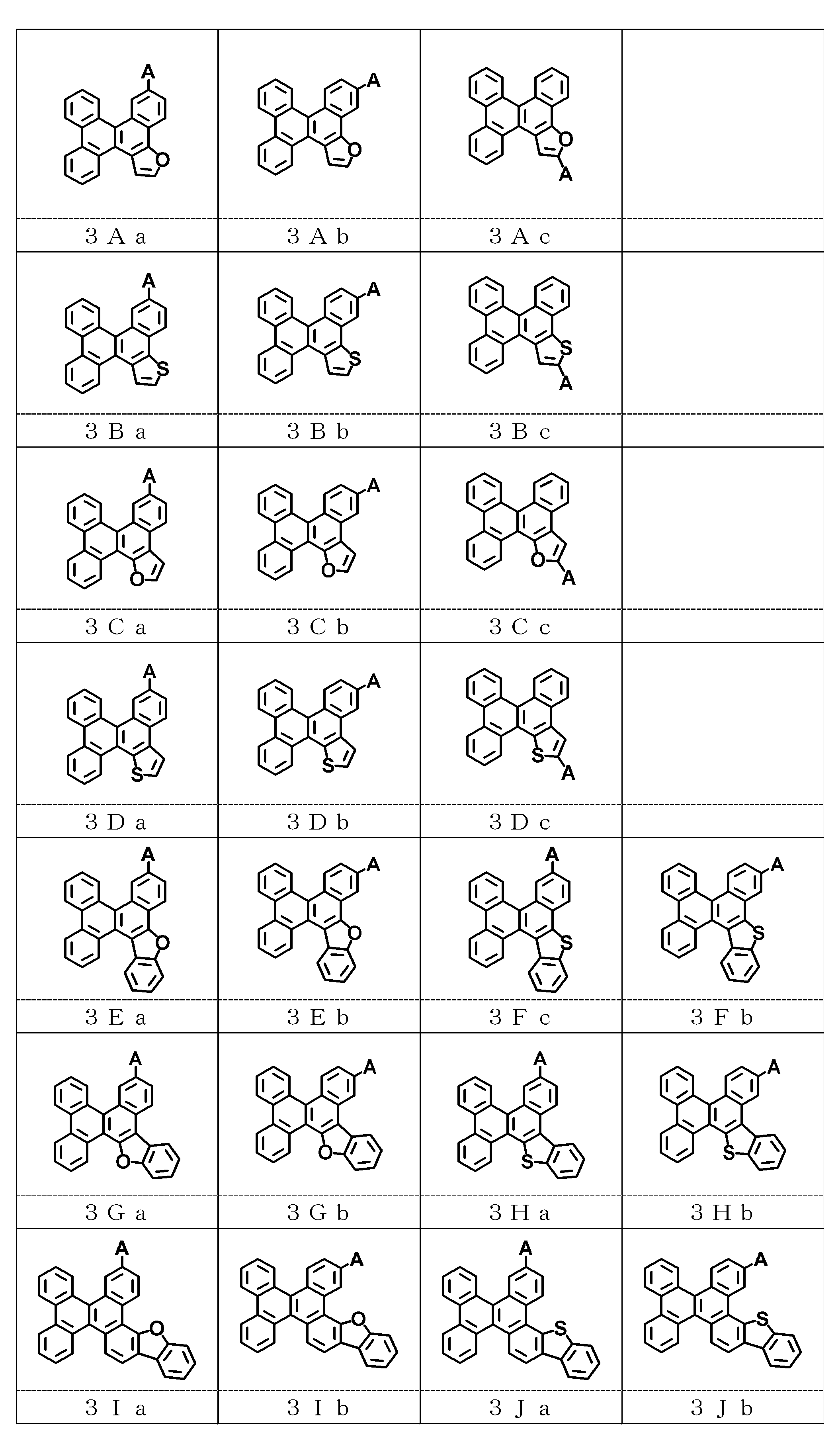
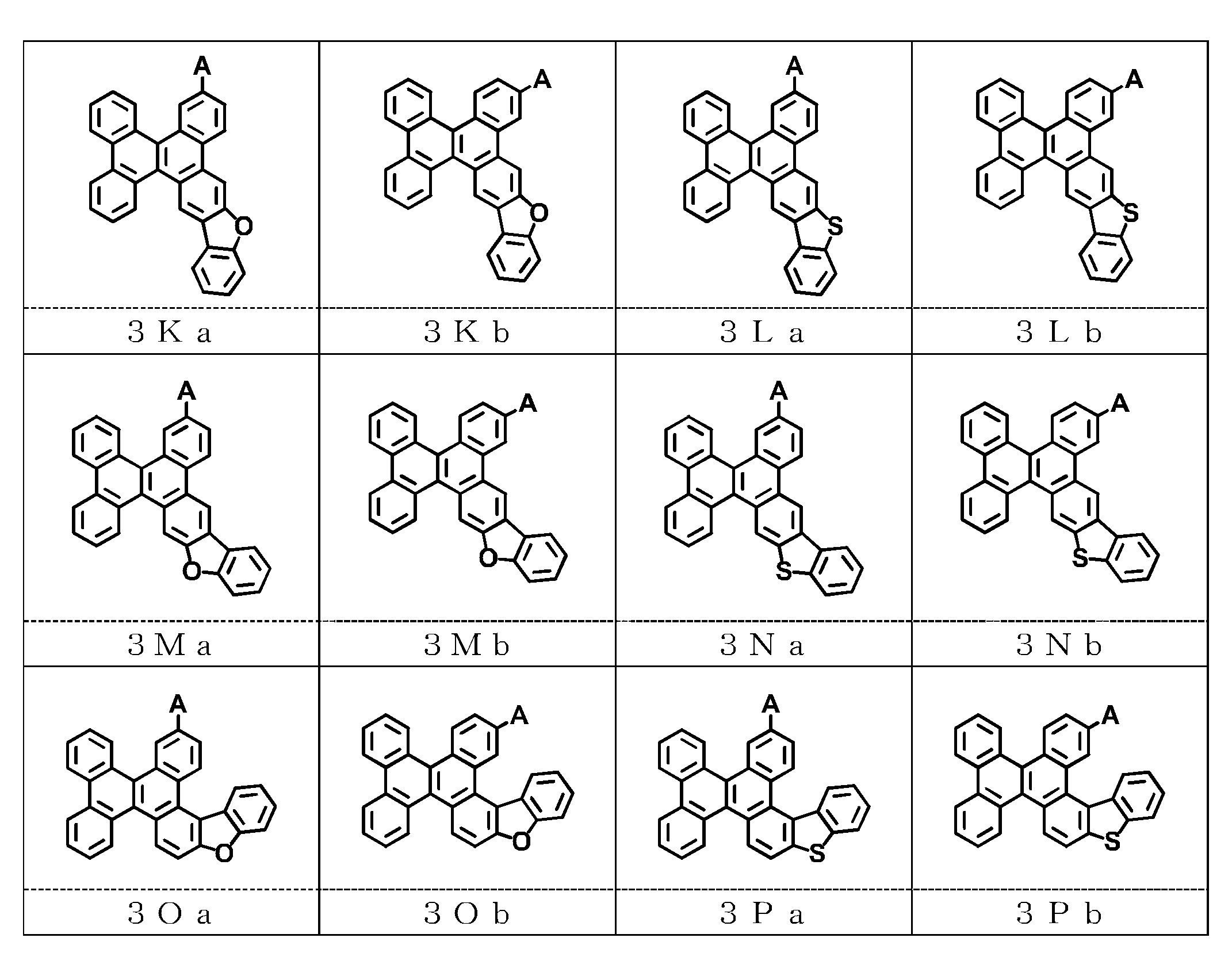
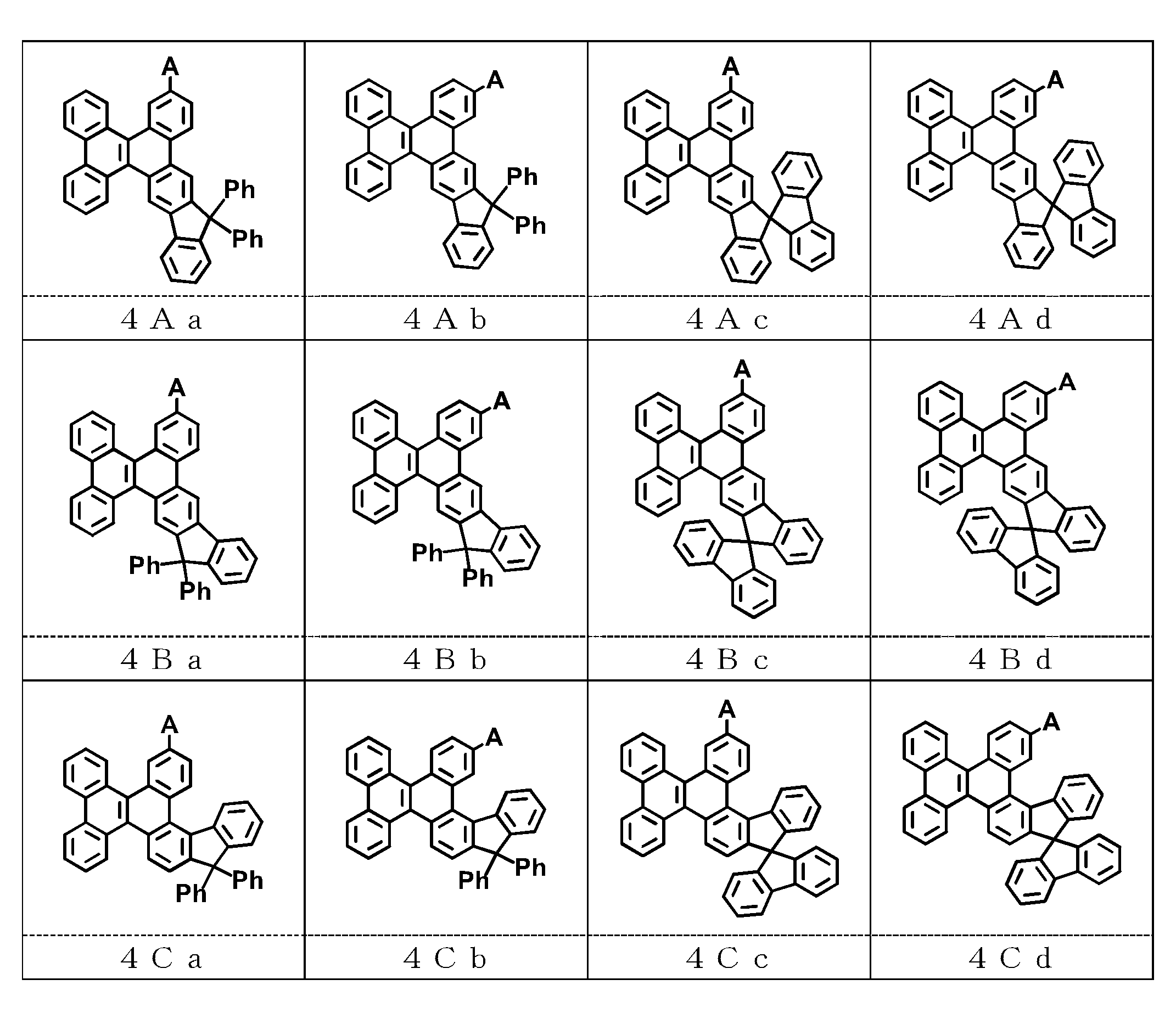
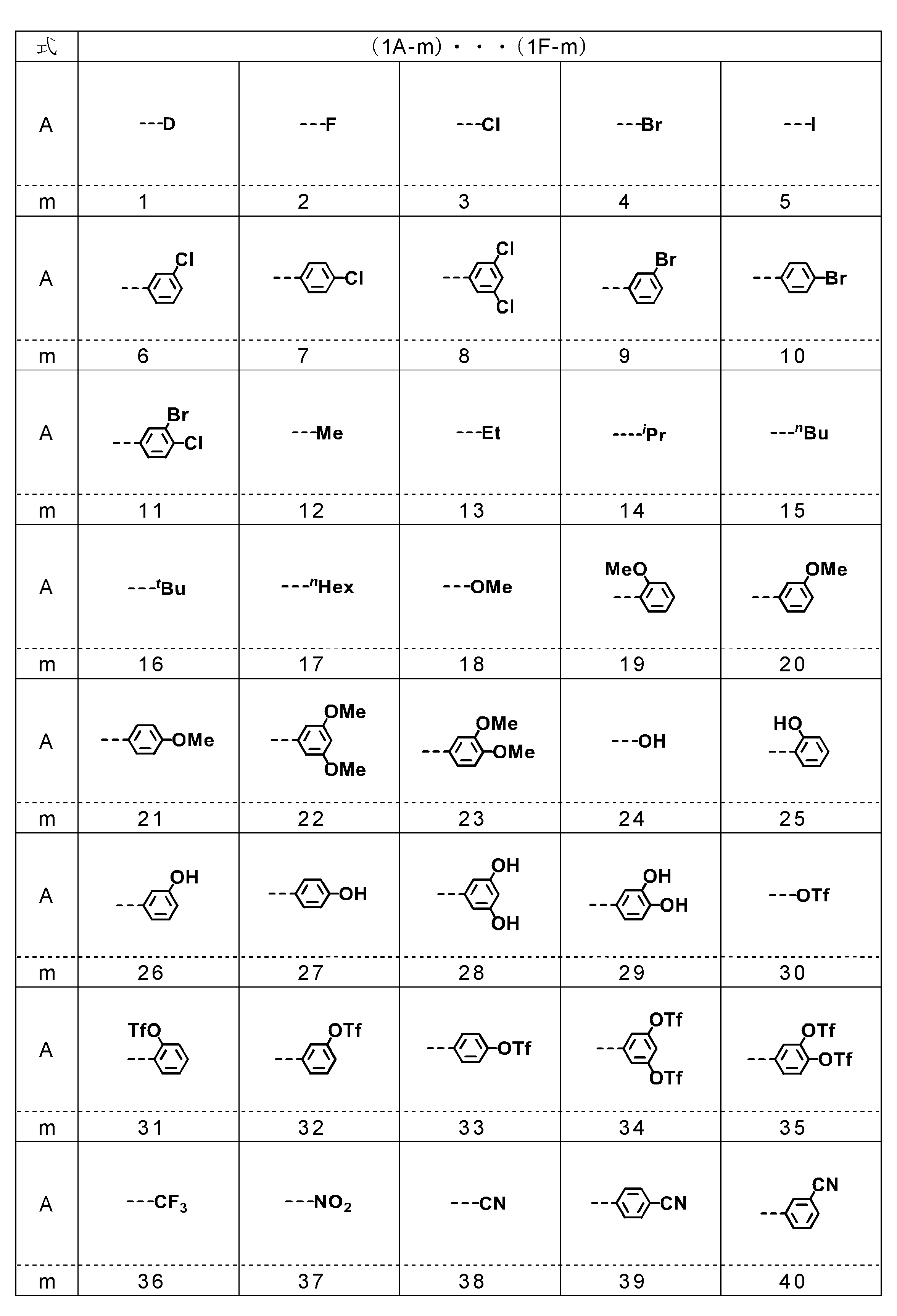
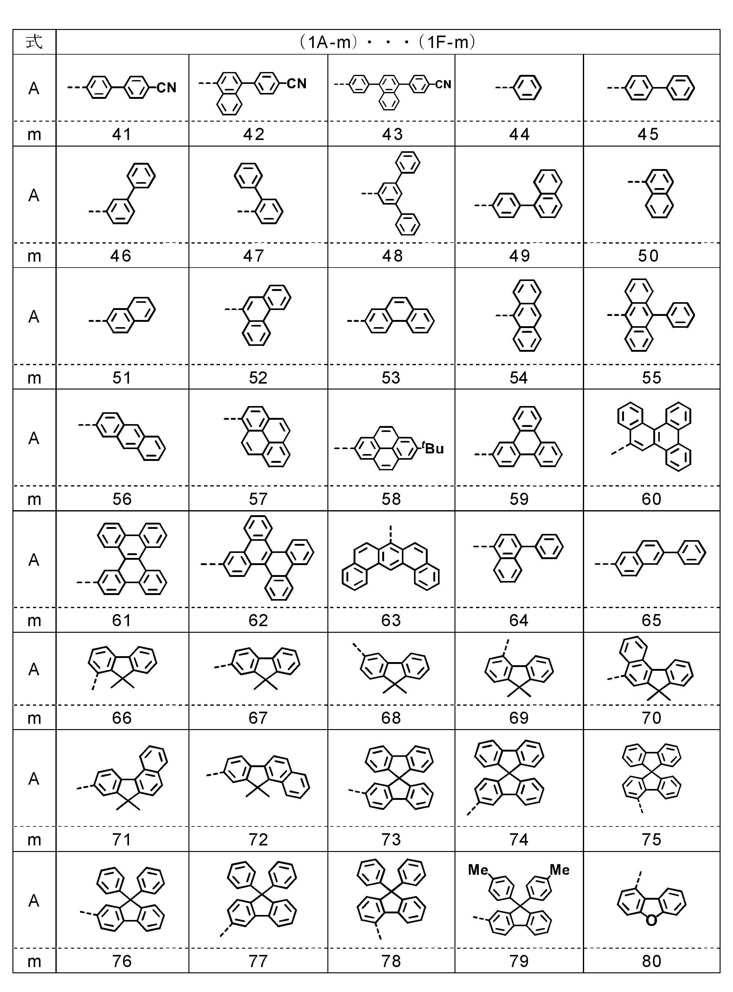


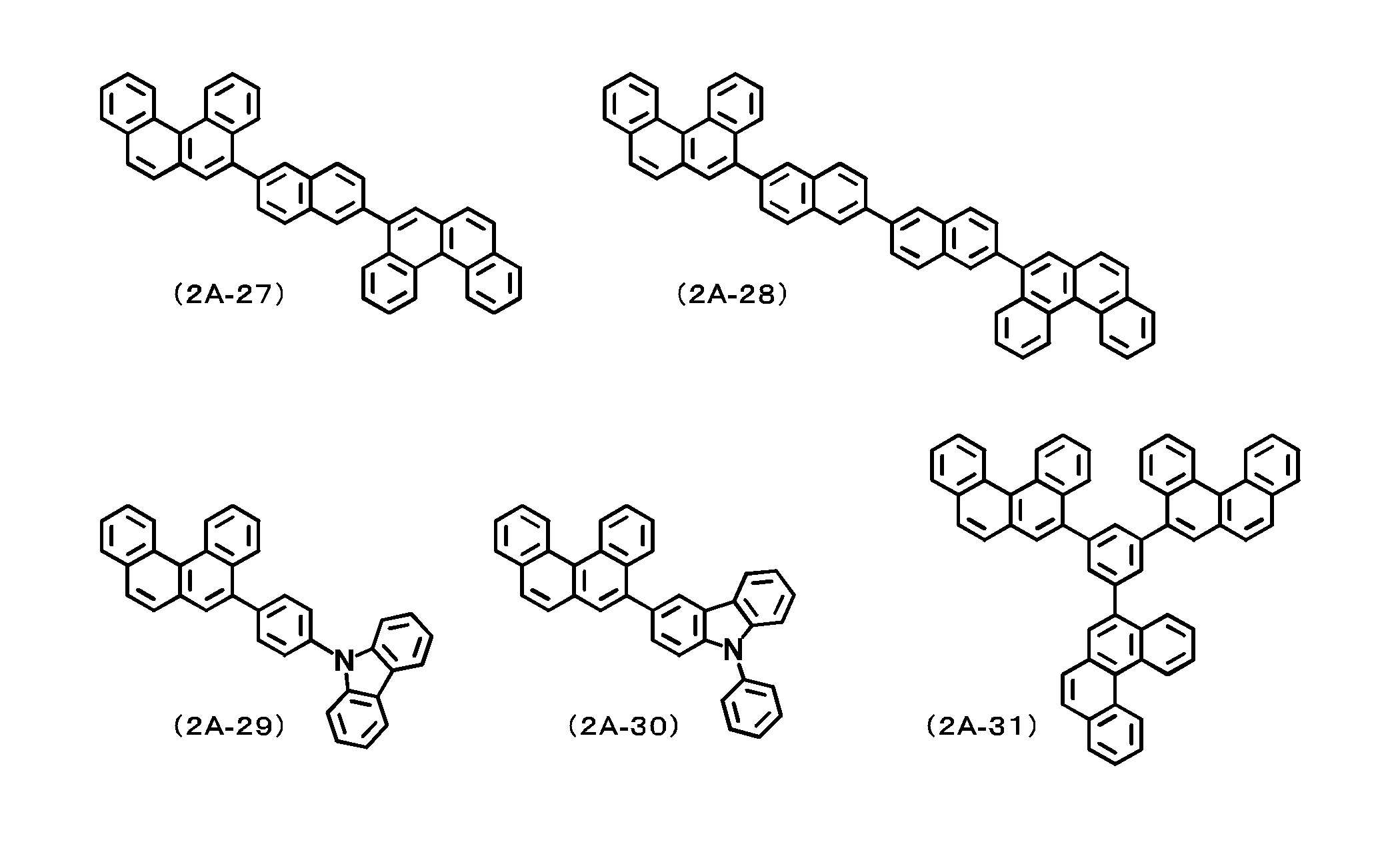

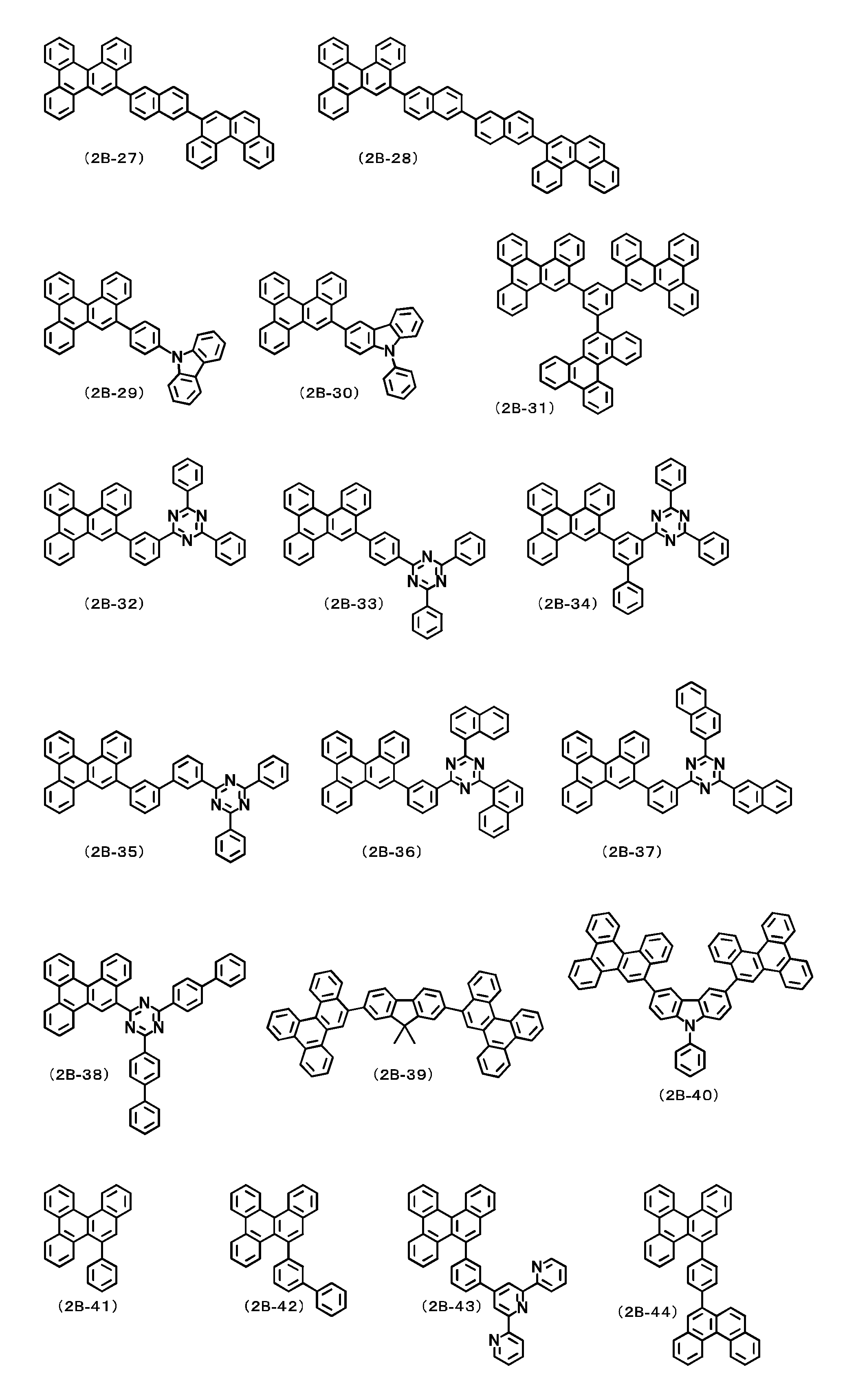
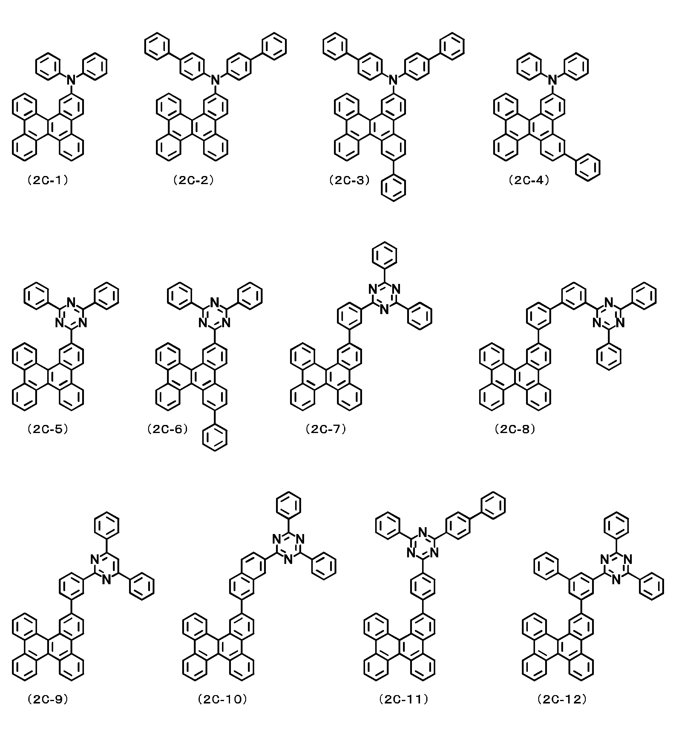


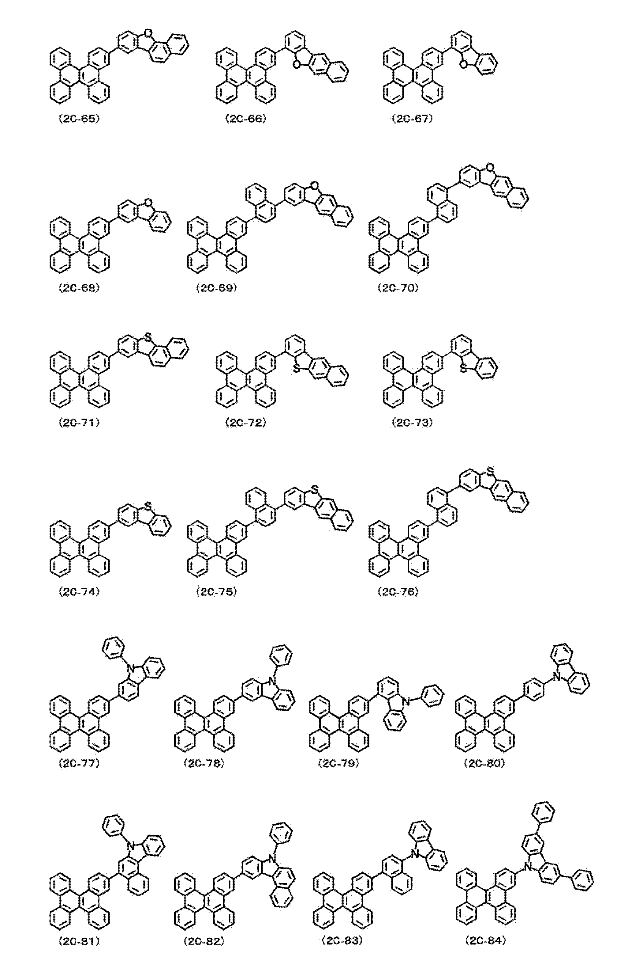

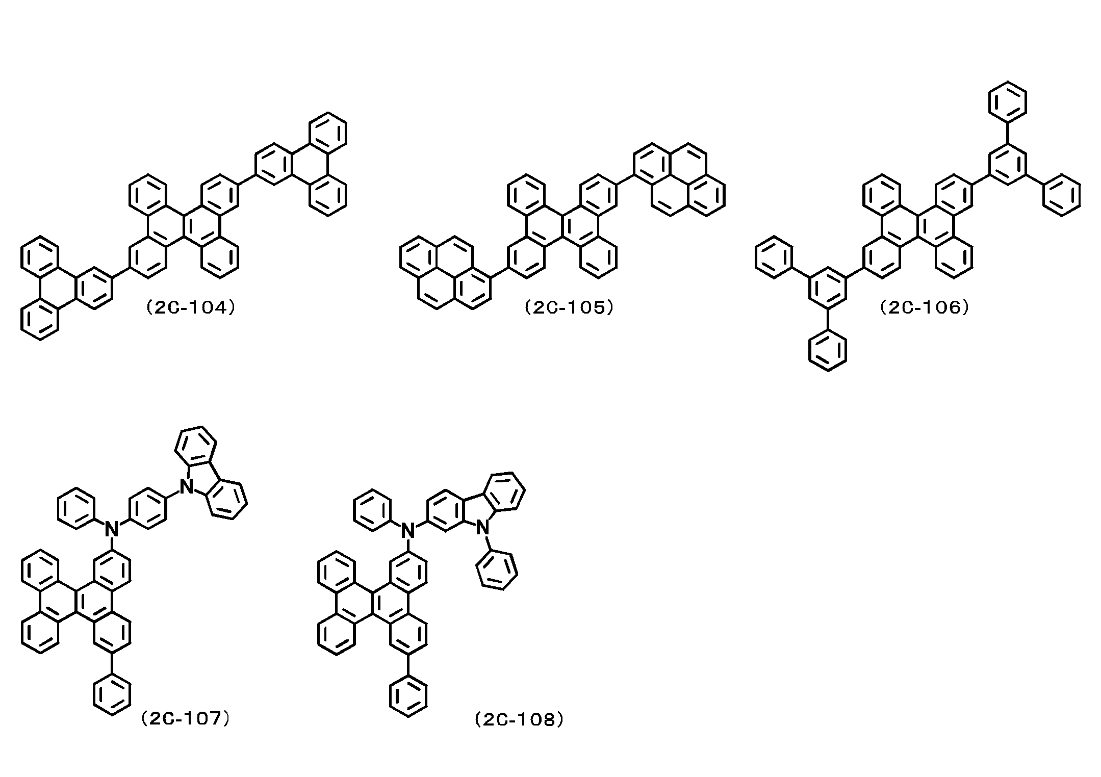


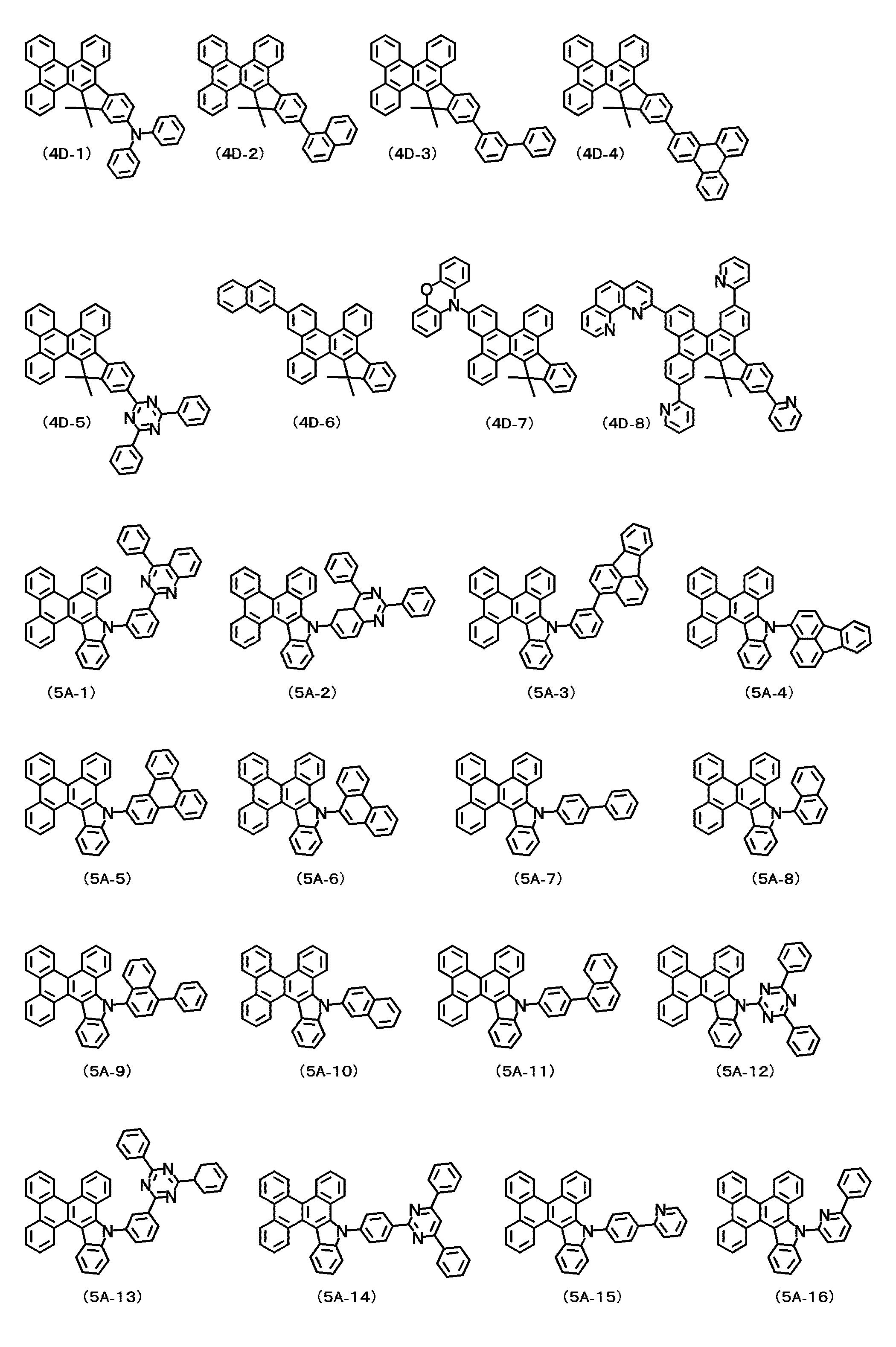

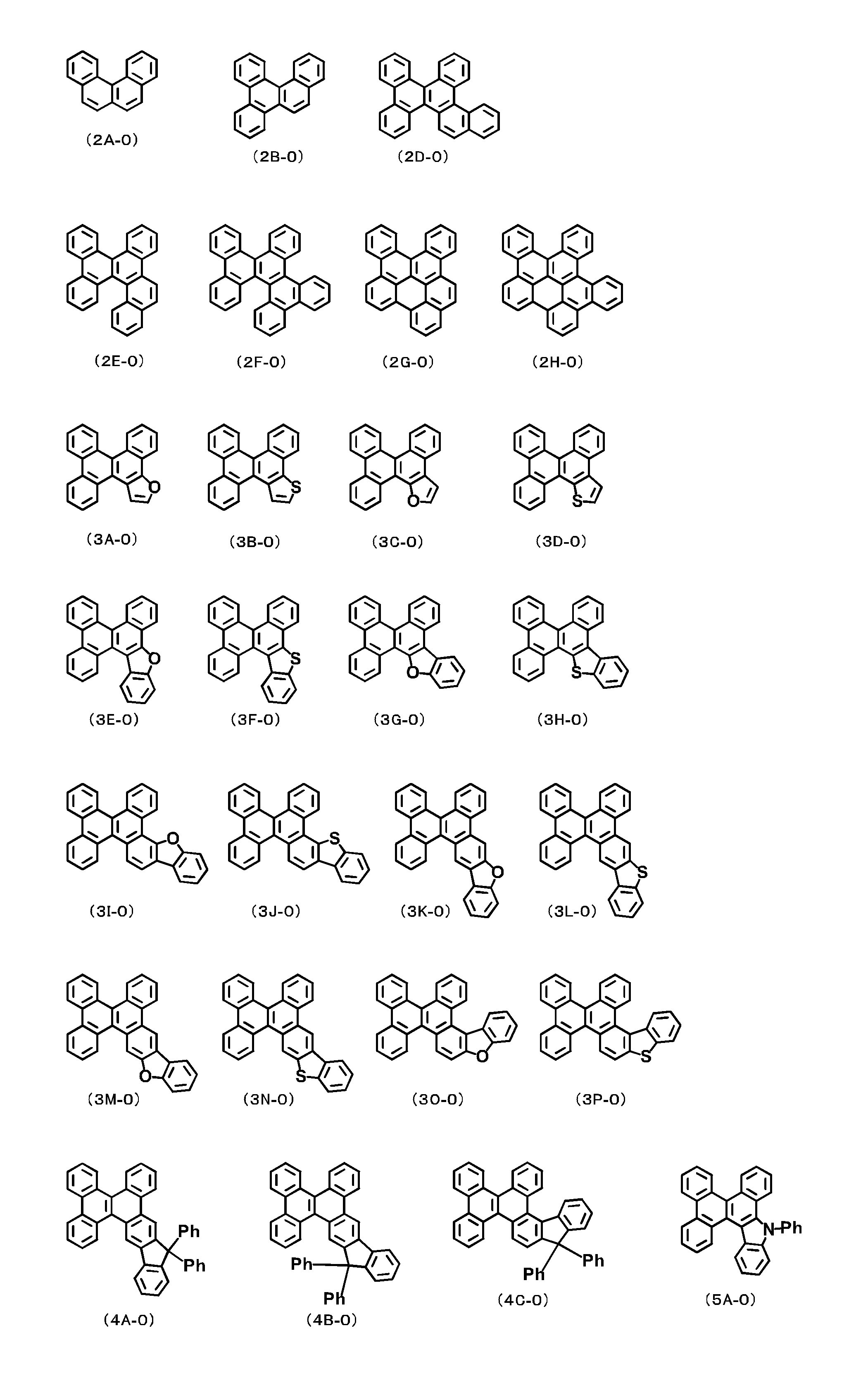
本発明の一態様にかかる撮像素子用光電変換素子用材料は、公知の材料を用いることができる。
撮像素子用光電変換素子用材料は、例えば、撮像素子用光電変換素子用輸送材料、撮像素子用光電変換素子用電荷ブロッキング材料として用いることができる。
本発明の一態様にかかる撮像素子用光電変換素子用材料または式(1)で示される撮像素子用光電変換素子用材料は、昇華時の耐熱安定性の観点から、分子量が1500以下であることが好ましく、1000以下であることがさらに好ましい。
本発明の一態様にかかる撮像素子用光電変換素子用材料または式(1)で示される撮像素子用光電変換素子用材料のHOMO準位は、特に限定されないが、撮像素子用光電変換素子への適合性の観点から、HOMOが5.0~6.5eVであることが好ましい。なお、このHOMO値は、蒸着膜に対して、大気中光電子収量分光装置による測定から得られた値である。
本発明の一態様にかかる撮像素子用光電変換素子用材料または式(1)で示される撮像素子用光電変換素子用材料のバンドギャップは、特に限定されないが、撮像素子用光電変換素子への適合性の観点から、バンドギャップが2.5~4.0eVであることが好ましい。なお、このバンドギャップは、蒸着膜の吸収スペクトルの波長端から得られた値である。
本発明の一態様にかかる撮像素子用光電変換素子用材料または式(1)で示される撮像素子用光電変換素子用材料のLUMO準位は、特に限定されないが、撮像素子用光電変換素子への適合性の観点から、LUMOが2.0~3.5eVであることが好ましい。なお、このLUMO値は、上記HOMO値およびバンドギャップから得られた値である。
本発明の一態様にかかる撮像素子用光電変換素子用材料または式(1)で示される撮像素子用光電変換素子用材料のガラス転移温度は、特に限定されないが、撮像素子用光電変換素子への適合性の観点から、ガラス転移温度が100℃以上であることが好ましく、110℃以上であることがより好ましく、130℃以上であることが特に好ましい。なお、このガラス転移温度は、示差走査熱量測定から得られた値である。
本発明の一態様にかかる撮像素子用光電変換素子用材料または式(1)で示される撮像素子用光電変換素子用材料は、該材料の蒸着膜がアモルファス層を形成するものが好ましい。蒸着膜が結晶層であると、隣接層との界面が均一にならないため、素子の欠陥要因になる。
蒸着膜がアモルファス層であるかの確認方法は、特に限定されないが、目視による結晶化の有無による判断、または蒸着膜のXRD測定により、シャープな回折ピークが観測されないこと等で確認できる。
本発明の一態様は、コーブ領域を有する化合物が撮像素子用光電変換素子用材料として有望であることを見出したことにある。式(1)で表される骨格においては、コーブ領域の存在によって、X1とX2の立体反発を解消するために共役系にねじれが生じることが知られている。この効果により、本発明の一態様である撮像素子用光電変換素子用材料は、従来の平面性の多環式の化合物を母核とした材料と比較して、蒸着膜でのアモルファス安定性に優れる。加えて、本発明の一態様である撮像素子用光電変換素子用材料は、共役系のねじれに起因して、母核どうしが重なり合う形でカラム状にスタッキングする効果が期待できる。
本発明の一態様である撮像素子用光電変換素子用材料は、コーブ領域を有するねじれた多環式化合物を母核としたことで、蒸着膜のアモルファス膜が安定で、且つ蒸着膜中においても母核どうしがある程度規則正しく配列し、良好な電荷輸送経路を確保したことで、撮像素子用光電変換素子における優れた暗電流を実現できたと推察している。更に、本発明の一態様は、該骨格が置換されることにより、HOMO準位の調整、ガラス転移温度の向上、アモルファス性の向上、電荷輸送性の向上、および逆電荷に対するブロッキング性の向上など、必要に応じた特性を付与することもできる。例えば、本発明の一態様である撮像素子用光電変換素子用材料を、後述する撮像素子用光電変換素子の正孔輸送層として用いた場合、良好に正孔を輸送すると同時に、逆電荷である電子をブロックする効果が期待できる。逆電荷をブロックすることで、撮像素子用光電変換素子における暗電流を抑制することができる。
本発明の一態様にかかる撮像素子用光電変換素子は、本発明の実施態様にかかる撮像素子用光電変換素子用材料を含む。
撮像素子用光電変換素子の構成については特に限定されないが、例えば、以下に示す(i)~(vi)の構成が挙げられる。
(ii):下部電極/正孔輸送層(電子ブロッキング層)/光電変換層/上部電極
(iii):下部電極/光電変換層/電子輸送層(正孔ブロッキング層)/上部電極
(iv):下部電極/正孔輸送層(電子ブロッキング層)/光電変換層/電子輸送層(正孔ブロッキング層)/上部電極
(v): 下部電極/バッファ層/正孔輸送層(電子ブロッキング層)/光電変換層/電子輸送層(正孔ブロッキング層)/上部電極
(vi):下部電極/正孔輸送層/電子ブロッキング層/光電変換層/正孔ブロッキング層/電子輸送層/上部電極
なお、バッファ層は、必要に応じて、他の名称または機能を有する層で置き換えても良い。他の名称または機能を有する層としては、例えば、仕事関数調整層などが挙げられる。
撮像素子用光電変換素子は、光電変換層、および、該光電変換層と下部電極との間の層からなる群より選ばれる1層以上に撮像素子用光電変換素子用材料を含む。したがって、図1に示される構成例において撮像素子用光電変換素子100は、光電変換層5および正孔輸送層4からなる群より選ばれる少なくとも1層に撮像素子用光電変換素子用材料を含む。特に、正孔輸送層4が撮像素子用光電変換素子用材料を含むことが好ましい。
基板としては特に限定はなく、例えばガラス板、石英板、プラスチック板等が挙げられる。また、基板1側から光が入射する構成の場合、基板1は光の波長に対して透明である。
基板1上には下部電極2が設けられている。
光が下部電極を通過して、光電変換層に入射する構成の撮像素子用光電変換素子の場合、下部電極は当該光を通すかまたは実質的に通す透明材料で形成される。
下部電極2と、後述する正孔輸送層4との間には、バッファ層3が設けられている。バッファ層3は、仕事関数を調整することで、正孔輸送層(電子ブロッキング層)4から正孔を効率よく受容する役割もあり、正孔注入層あるいは仕事関数調整層とも呼ばれる。従来公知のバッファ層3の具体例としては、ナフタレン-1,4,5,8-テトラカルボン酸二無水物(NTCDA)、2,3,6,7,10,11-ヘキサシアノ-1,4,5,8,9,12-ヘキサアザトリフェニレン(HATCN)などが挙げられる。
バッファ層3と光電変換層5との間には、正孔輸送層(電子ブロッキング層とも呼ばれる)4が設けられている。
これらの中でも、フルオレン化合物、ナフトジチオフェン化合物、ナフトチエノチオフェン化合物、ベンゾジフラン化合物、ベンゾチオフェン化合物、ナフトビスベンゾチオフェン化合物、クリセノジチオフェン化合物、ベンゾチエノベンゾチオフェン化合物、インドロカルバゾール化合物等が好ましく、特にフルオレン化合物、クリセノジチオフェン化合物、ベンゾチエノベンゾチオフェン化合物、インドロカルバゾール化合物が好ましい。

正孔輸送層4と後述する電子輸送層6との間には、光電変換層5が設けられている。
光電変換層5の材料としては、光電変換機能を有する材料が挙げられる。
一種の材料からなる単層構造である光電変換層5に用いられる材料としては、例えば、(1)クマリンおよびその誘導体、キナクリドンおよびその誘導体、フタロシアニンおよびその誘導体などが挙げられる。
二種の材料からなる単層構造である光電変換層5に用いられる材料としては、例えば、前述の(i)クマリンおよびその誘導体、キナクリドンおよびその誘導体、フタロシアニンおよびその誘導体と、(ii)フラーレンおよびその誘導体との組み合わせが挙げられる。これらの材料からなる光電変換層5の作製は、予め粉末を混合した状態で蒸着させて形成しても良いし、任意の割合で共蒸着することで形成しても良い。
三種の材料からなる単層構造である光電変換層5に用いられる材料としては、前述の(i)クマリンおよびその誘導体、キナクリドンおよびその誘導体、フタロシアニンおよびその誘導体、(ii)フラーレンおよびその誘導体、および(iii)正孔輸送材料との組み合わせが挙げられる。これらの材料からなる光電変換層5の作製は、予め粉末を混合した状態で蒸着させて形成しても良いし、任意の割合で共蒸着することで形成しても良い。
(ii)フラーレンおよびその誘導体の具体例としては、[60]フラーレン、[70]フラーレン、[6,6]-フェニル-C61-酪酸メチル([60]PCBM)が挙げられる。
(iii)正孔輸送材料の好ましい化合物および具体例としては、前述の正孔輸送層4で記載したものと同じものが挙げられる。
光電変換層5と後述する上部電極7との間には、電子輸送層(正孔ブロッキング層とも呼ばれる)6が設けられている。
電子輸送層6は、光電変換層5で発生した電子を上部電極7側へ輸送する役割と、光電変換層5で発生した正孔が上部電極7側へ移動するのをブロックする役割とを有する。
電子輸送層6上には上部電極7が設けられている。
上部電極7の材料としては、ナトリウム、ナトリウム-カリウム合金、マグネシウム、リチウム、マグネシウム/銅混合物、銀、マグネシウム/銀混合物、マグネシウム/アルミニウム混合物、マグネシウム/インジウム混合物、アルミニウム/酸化アルミニウム(Al2O3)混合物、インジウム、リチウム/アルミニウム混合物、希土類金属等が挙げられる。
以上説明した下部電極2、上部電極7を除く各層は、それぞれの層の材料(必要に応じて結着樹脂等の材料、溶剤と共に)を、例えば真空蒸着法、スピンコート法、キャスト法、LB(Langmuir-Blodgett method)法等の公知の方法によって薄膜化することにより、形成することができる。
このようにして形成された各層の膜厚については特に制限はなく、状況に応じて適宜選択することができるが、通常は5nm以上5μm以下の範囲である。
同じ材料を用いる具体例としては、例えば、下部電極2がITOの際、スパッタリング法を用いて、上部電極7をITO層として形成した場合などが挙げられる。このような構造の場合、光は上部電極7を通過して、光電変換層5に入射する構成の撮像素子用光電変換素子となる。
また、下部電極2および上部電極7を構成する材料を入れ替える場合、上記(v)の構成と逆の順序で層を積層しても良い。例えば、下記(I)~(IV)に示す構成が挙げられる。
(I):下部電極/電子輸送層(正孔ブロッキング層)/光電変換層/上部電極
(II):下部電極/光電変換層/正孔輸送層(電子ブロッキング層)/上部電極
(III):下部電極/電子輸送層(正孔ブロッキング層)/光電変換層/正孔輸送層(電子ブロッキング層)/上部電極
(IV):下部電極/電子輸送層(正孔ブロッキング層)/光電変換層/正孔輸送層(電子ブロッキング層)/バッファ層/上部電極
上記(IV)の構成において、下部電極および上部電極が(v)の構成と同様に、それぞれ、透明材料および透明性がない材料の場合、光は下部電極を通過して、光電変換層に入射する構成の撮像素子用光電変換素子となるが、印加する電圧は前述した(v)の構成とは逆方向になる(逆バイアスとも呼ばれる)。すなわち、光電変換層で発生した正孔および電子を、それぞれ、上部電極側および下部電極側へ輸送するように電圧を印加する。また、上記の構成において、バッファ層は上部電極をスパッタリング法により形成する際の、有機膜へのダメージを低減する役割がある。
図2に示すように、基板1、下部電極2、正孔輸送層4、光電変換層5、電子輸送層6、上部電極7からなる積層構成を有する撮像素子用光電変換素子101を作製し、該光電変換素子の暗電流を評価した。
下部電極をその表面に備えた基板として、2mm幅の酸化インジウム-スズ(ITO)膜(膜厚110nm)がストライプ状にパターンされたITO透明電極付きガラス基板を用意した。ついで、この基板をイソプロピルアルコールで洗浄した後、オゾン紫外線洗浄にて表面処理を行った。
洗浄後の表面処理が施された基板上に、真空蒸着法で各層の真空蒸着を行い、各層を積層形成した。
まず、真空蒸着槽内に前記ガラス基板を導入し、7.0×10⁻⁵Paまで減圧した。そして、以下の順で、各層の成膜条件に従ってそれぞれ作製した。
昇華精製した化合物(2C-7)を0.15nm/秒の速度で30nm成膜し、正孔輸送層4を作製した。なお、本構成においては、下部電極2と正孔輸送層4との間のバッファ層は作製しなかった。
N,N-ジメチルキナクリドンを0.30nm/秒の速度で100nm成膜し、光電変換層5を作製した。
トリス(8-ヒドロキシキノリナート)アルミニウムを0.15nm/秒の速度で30nm成膜し、電子輸送層6を作製した。
最後に、基板上のITOストライプと直行するようにメタルマスクを配し、上部電極7を成膜した。上部電極は、アルミニウムを100nm成膜した。アルミニウムの成膜速度は3nm/秒であった。
素子実施例A-1において、化合物(2C-7)の代わりに、それぞれ、順に、化合物(2C-25)、(3Ja-186)、2,7-ジフェニル[1]ベンゾチエノ[3,2-b] [1]ベンゾチオフェン(DiPh-BTBT)を用いた以外は、素子実施例A-1と同じ方法で撮像素子用光電変換素子を作製し、評価した。得られた測定結果を表1に示す。

図3に示すように、基板1、下部電極2、電子輸送層6、光電変換層5、正孔輸送層4、バッファ層3、上部電極7からなる積層構成を有する撮像素子用光電変換素子102を作製し、該光電変換素子の暗電流と外部量子効率を評価した。
基板1および下部電極2の用意については、素子実施例A-1と同様の手順で実施した。
昇華精製した化合物4,6-ビス(3,5-ジ(ピリジン-4-イル)フェニル)-2-メチルピリミジンを0.10nm/秒の速度で10nm成膜し、電子輸送層6を作製した。
N,N-ジメチルキナクリドンおよびC60を4:1(質量比)の割合で120nm成膜し、光電変換層5を作製した。成膜速度は0.15nm/秒であった。
昇華精製した化合物(2C-1)を0.10nm/秒の速度で10nm成膜し、正孔輸送層4を作製した。
昇華精製した化合物2,3,6,7,10,11-ヘキサシアノ-1,4,5,8,9,12-ヘキサアザトリフェニレン(HATCN)を0.10nm/秒の速度で10nm成膜し、バッファ層3を作製した。
最後に、基板上のITOストライプと直行するようにメタルマスクを配し、上部電極7を成膜した。上部電極は、銀を80nm成膜した。銀の成膜速度は0.1nm/秒であった。
素子実施例B-1の正孔輸送層(電子ブロッキング層)4の作製において、化合物(2C-1)の代わりに、それぞれ化合物(2C-2)、化合物(2C-3)、化合物(2C-7)、化合物(2C-8)、化合物(2C-12)、化合物(2C-13)、化合物(2C-26)、化合物(2C-32)、化合物(2C-61)、化合物(2C-107)、化合物(2C-108)、化合物(3Eb-194)、化合物(3Ia-91)、化合物(3Ia-194)、化合物(3Oa-88)、化合物(4Ac-192)、化合物(4Bb-192)、化合物(5A-0)、または2,7-ジフェニル[1]ベンゾチエノ[3,2-b] [1]ベンゾチオフェン(DiPh-BTBT)を用いたこと以外は、素子実施例B-1と同様の方法により、それぞれ素子実施例B-2~B-19および素子比較例B-1の撮像素子用光電変換素子を作製し、素子実施例B-1と同じ方法により暗電流および外部量子効率を測定した。結果を表2に示す。
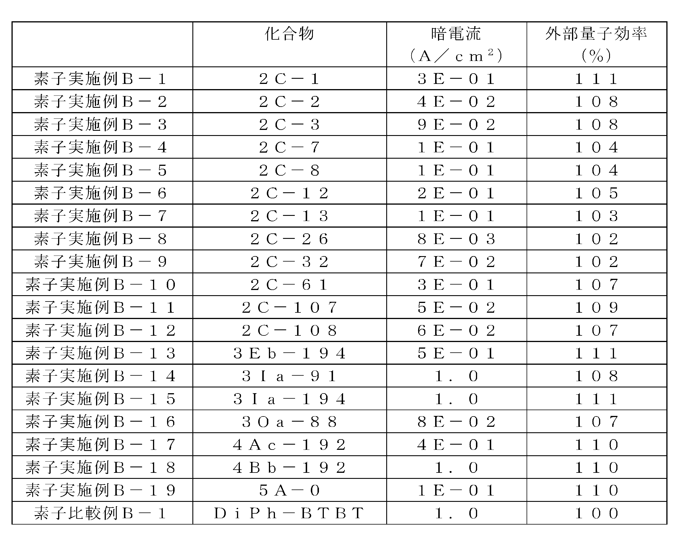
2 下部電極
3 バッファ層
4 正孔輸送層(電子ブロッキング層)
5 光電変換層
6 電子輸送層(正孔ブロッキング層)
7 上部電極
100 撮像素子用光電変換素子
101 撮像素子用光電変換素子
102 撮像素子用光電変換素子
Claims (20)
- 分子構造中にコーブ(cove)領域を有する骨格を含み、該骨格が置換されていてもよい化合物を含み、
ただし、該化合物として、無置換のジベンゾ[g,p]クリセンを含まない、
撮像素子用光電変換素子用材料。 - 前記骨格が、下記式(1)で表される、請求項1に記載の撮像素子用光電変換素子用材料。

X1~X4は、それぞれ独立して、水素原子または置換基を表し;
X1~X4は、互いに結合して環を形成することはなく;
複数のX1~X4は、同一であっても異なっていてもよく;
Z1~Z8は、それぞれ独立して、窒素原子、または置換基を有していてもよい炭素原子を表し;
Z1~Z8の内、少なくとも6つは置換基を有していてもよい炭素原子であり;
複数のZ1~Z8は、同一であっても異なっていてもよく;
Z1~Z8のいずれかが、置換基を有する炭素原子の場合、該炭素原子に隣接する1つあるいは2つのZ1~Z8いずれかの炭素原子上の置換基と結合し、環を形成してもよい。) - Z1~Z8の内、少なくとも7つが置換基を有していてもよい炭素原子である、請求項2に記載の撮像素子用光電変換素子用材料。
- Z1~Z8が置換基を有していてもよい炭素原子である、請求項2に記載の撮像素子用光電変換素子用材料。
- X1およびX2が水素原子である、請求項2~4のいずれか1項に記載の撮像素子用光電変換素子用材料。
- Z3およびZ4が置換基を有していてもよい炭素原子であり、Z3およびZ4の置換基が互いに結合して環を形成している、請求項2~5のいずれか1項に記載の撮像素子用光電変換素子用材料。
- 下記式(2A)~(5B)のいずれかで表される化合物を含む、撮像素子用光電変換素子用材料。
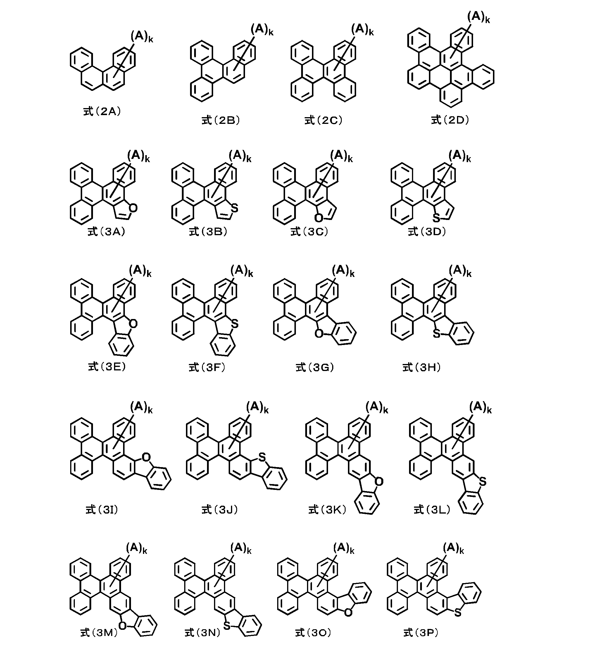
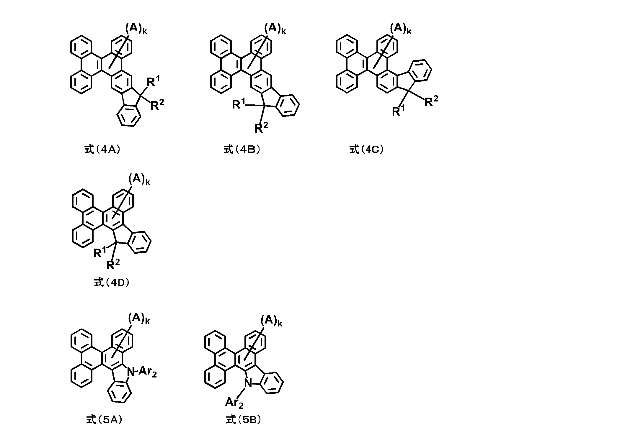
Aは電荷輸送性置換基を表し;
Ar2は置換基を有していてもよい炭素数6~30の単環、連結、もしくは縮環の芳香族炭化水素基、置換基を有していてもよい炭素数3~36の単環、連結、もしくは縮環のヘテロ芳香族基、および炭素数1~18の直鎖もしくは分岐のアルキル基を表し;
R1およびR2は、それぞれ独立して、
水素原子;
重水素原子;
置換基を有していてもよい炭素数6~30の単環、連結、若しくは縮環の芳香族炭化水素基;
置換基を有していてもよい炭素数3~36の単環、連結、若しくは縮環のヘテロ芳香族基;
炭素数1~18の直鎖もしくは分岐のアルキル基;
または、炭素数1~18の直鎖もしくは分岐のアルコキシ基を表し;
R1およびR2は、互いに結合して環を形成していてもよい。
kは1~4の整数を表し;
複数のAは同一であっても異なっていてもよい。) - 前記電荷輸送性置換基が、それぞれ独立して、
重水素原子;
フッ素原子、塩素原子、臭素原子、ヨウ素原子;
トリフルオロメチル基、ペンタフルオロエチル基;
シアノ基;
ニトロ基;
ヒドロキシル基;
チオール基;
置換基を有していてもよい炭素数6~30の単環、連結、もしくは縮環の芳香族炭化水素基;
置換基を有していてもよい炭素数3~36の単環、連結、もしくは縮環のヘテロ芳香族基;
置換基を有していてもよいホスフィンオキシド基;
置換基を有していてもよいシリル基;
炭素数2~10の飽和炭化水素基を有していてもよいボロニル基;
炭素数1~18の直鎖もしくは分岐のアルキル基;
炭素数1~18の直鎖もしくは分岐のアルコキシ基;
トリフルオロメチルスルホニルオキシ基;または、
下記式(6)もしくは(6’)で表される基である、請求項7に記載の撮像素子用光電変換素子用材料。

R100~R300は、それぞれ独立して、
水素原子、重水素原子;
置換基を有していてもよい炭素数6~30の単環、連結、もしくは縮環の芳香族炭化水素基;
置換基を有していてもよい炭素数3~36の単環、連結、もしくは縮環のヘテロ芳香族基;または、
炭素数1~18の直鎖もしくは分岐のアルキル基を表し;
Lは、それぞれ独立して、
メチル基もしくはフェニル基で置換されていてもよいフェニレン基、
メチル基もしくはフェニル基で置換されていてもよいナフチレン基、
メチル基もしくはフェニル基で置換されていてもよいビフェニレン基、または
単結合を表し;
nは、1または2を表し;
Lが単結合の場合、nは1であり;
Lが単結合ではない場合、nは1または2であり;
nが2の場合、複数のR100またはR200は、同一であっても異なっていてもよい。) - 分子量が1500以下である、請求項1~8のいずれか1項に記載の撮像素子用光電変換素子用材料。
- 分子量が1000以下である、請求項1~9のいずれか1項に記載の撮像素子用光電変換素子用材料。
- HOMO値が5.0~6.5eVである、請求項1~10のいずれか1項に記載の撮像素子用光電変換素子用材料。
- バンドギャップが2.5~4.0eVである、請求項1~11のいずれか1項に記載の撮像素子用光電変換素子用材料。
- LUMO値が2.0~3.5eVである、請求項1~12のいずれか1項に記載の撮像素子用光電変換素子用材料。
- ガラス転移温度が100℃以上である、請求項1~13のいずれか1項に記載の撮像素子用光電変換素子用材料。
- ガラス転移温度が110℃以上である、請求項1~14のいずれか1項に記載の撮像素子用光電変換素子用材料。
- ガラス転移温度が130℃以上である、請求項1~15のいずれか1項に記載の撮像素子用光電変換素子用材料。
- 撮像素子用光電変換素子用輸送材料または撮像素子用光電変換素子用電荷ブロッキング材料である、請求項1~16のいずれか1項に記載の撮像素子用光電変換素子用材料。
- 撮像素子用光電変換素子用正孔輸送材料または撮像素子用光電変換素子用電子ブロッキング材料である、請求項1~17のいずれか1項に記載の撮像素子用光電変換素子用材料。
- 請求項1~18のいずれか1項に記載の撮像素子用光電変換素子用材料を含む、撮像素子用光電変換素子。
- 前記撮像素子用光電変換素子用材料の蒸着膜がアモルファス層である、請求項19に記載の撮像素子用光電変換素子。
Priority Applications (5)
| Application Number | Priority Date | Filing Date | Title |
|---|---|---|---|
| KR1020237043082A KR20240007274A (ko) | 2021-06-11 | 2022-06-08 | 촬상 소자용 광전 변환 소자용 재료 및 촬상 소자용 광전 변환 소자 |
| EP22820275.0A EP4342883A4 (en) | 2021-06-11 | 2022-06-08 | PHOTOELECTRIC CONVERSION ELEMENT MATERIAL FOR IMAGING ELEMENT AND PHOTOELECTRIC CONVERSION ELEMENT FOR IMAGING ELEMENT |
| EP25190729.1A EP4613746A3 (en) | 2021-06-11 | 2022-06-08 | Photoelectric conversion element material for imaging element and photoelectric conversion element for imaging element |
| CN202280040522.7A CN117440940A (zh) | 2021-06-11 | 2022-06-08 | 用于摄像元件用光电转换元件的材料及摄像元件用光电转换元件 |
| JP2023527904A JP7775883B2 (ja) | 2021-06-11 | 2022-06-08 | 撮像素子用光電変換素子用材料および撮像素子用光電変換素子 |
Applications Claiming Priority (4)
| Application Number | Priority Date | Filing Date | Title |
|---|---|---|---|
| JP2021098353 | 2021-06-11 | ||
| JP2021-098353 | 2021-06-11 | ||
| JP2022-001855 | 2022-01-07 | ||
| JP2022001855 | 2022-01-07 |
Publications (1)
| Publication Number | Publication Date |
|---|---|
| WO2022260096A1 true WO2022260096A1 (ja) | 2022-12-15 |
Family
ID=84426103
Family Applications (1)
| Application Number | Title | Priority Date | Filing Date |
|---|---|---|---|
| PCT/JP2022/023166 Ceased WO2022260096A1 (ja) | 2021-06-11 | 2022-06-08 | 撮像素子用光電変換素子用材料および撮像素子用光電変換素子 |
Country Status (5)
| Country | Link |
|---|---|
| EP (2) | EP4342883A4 (ja) |
| JP (1) | JP7775883B2 (ja) |
| KR (1) | KR20240007274A (ja) |
| TW (1) | TW202313570A (ja) |
| WO (1) | WO2022260096A1 (ja) |
Cited By (1)
| Publication number | Priority date | Publication date | Assignee | Title |
|---|---|---|---|---|
| WO2026004765A1 (ja) * | 2024-06-24 | 2026-01-02 | 東ソー株式会社 | 撮像素子用光電変換素子用材料、アミン化合物、有機電子素子用材料、光電変換素子用材料、有機薄膜、および有機電子素子 |
Families Citing this family (1)
| Publication number | Priority date | Publication date | Assignee | Title |
|---|---|---|---|---|
| JP7775883B2 (ja) | 2021-06-11 | 2025-11-26 | 東ソー株式会社 | 撮像素子用光電変換素子用材料および撮像素子用光電変換素子 |
Citations (13)
| Publication number | Priority date | Publication date | Assignee | Title |
|---|---|---|---|---|
| JP2010258438A (ja) | 2009-03-30 | 2010-11-11 | Fujifilm Corp | 光電変換素子及び撮像素子 |
| JP2011006397A (ja) | 2009-05-29 | 2011-01-13 | Chisso Corp | ジベンゾ[g,p]クリセン化合物、該化合物を含有する発光層用材料、およびこれを用いた有機電界発光素子 |
| JP4968333B2 (ja) | 2008-02-27 | 2012-07-04 | 東レ株式会社 | 発光素子材料および発光素子 |
| WO2017109722A1 (en) | 2015-12-21 | 2017-06-29 | Idemitsu Kosan Co., Ltd. | Nitrogen-containing heterocyclic compounds and organic electroluminescence devices containing them |
| JP2018193371A (ja) | 2017-05-17 | 2018-12-06 | 東ソー株式会社 | 縮合環化合物 |
| JP2019034939A (ja) | 2017-08-18 | 2019-03-07 | 東ソー株式会社 | ジベンゾ[g,p]クリセン化合物 |
| JP2019034933A (ja) | 2017-08-10 | 2019-03-07 | 東ソー株式会社 | 縮合環化合物、その製法、及びその製造中間体 |
| US20190198781A1 (en) | 2017-12-26 | 2019-06-27 | Luminescence Technology Corporation | Organic compound and organic electroluminescence device using the same |
| JP2019116472A (ja) | 2017-12-26 | 2019-07-18 | 東ソー株式会社 | 縮合環化合物および有機エレクトロルミネッセンス素子用材料 |
| JP2020015691A (ja) | 2018-07-25 | 2020-01-30 | 東ソー株式会社 | 縮合環化合物 |
| JP2020033332A (ja) | 2018-03-30 | 2020-03-05 | 東ソー株式会社 | 縮合環化合物、その製法、及びその製造中間体 |
| JP2021098353A (ja) | 2019-12-23 | 2021-07-01 | 均 深尾 | 複合樹脂成形体の成形方法 |
| JP2022001855A (ja) | 2020-06-22 | 2022-01-06 | マツダ株式会社 | 電極部装置、被覆金属材の耐食性試験方法及び耐食性試験装置 |
Family Cites Families (10)
| Publication number | Priority date | Publication date | Assignee | Title |
|---|---|---|---|---|
| KR101551207B1 (ko) * | 2008-09-04 | 2015-09-08 | 롬엔드하스전자재료코리아유한회사 | 신규한 유기 발광 화합물 및 이를 발광재료로서 채용하고 있는 유기 발광 소자 |
| DE102009005746A1 (de) * | 2009-01-23 | 2010-07-29 | Merck Patent Gmbh | Materialien für organische Elektrolumineszenzvorrichtungen |
| JP4795463B2 (ja) * | 2009-12-02 | 2011-10-19 | キヤノン株式会社 | 新規ベンゾ[c]フェナンスレン化合物及びこれを有する有機発光素子 |
| KR20130067312A (ko) * | 2009-12-16 | 2013-06-21 | 이데미쓰 고산 가부시키가이샤 | 유기 발광 매체 |
| KR102330625B1 (ko) | 2014-04-25 | 2021-11-23 | 닛뽄 가야쿠 가부시키가이샤 | 촬상 소자용 광전 변환 소자용 재료 및 그것을 포함하는 광전 변환 소자 |
| JP6754156B2 (ja) * | 2015-06-15 | 2020-09-09 | ソニーセミコンダクタソリューションズ株式会社 | 固体撮像素子および固体撮像素子の製造方法、光電変換素子、撮像装置、電子機器、並びに光電変換素子。 |
| JP2019186500A (ja) * | 2018-04-17 | 2019-10-24 | ソニー株式会社 | 光電変換素子および撮像装置 |
| TWI882870B (zh) | 2018-07-26 | 2025-05-01 | 日商索尼股份有限公司 | 光電轉換元件 |
| KR20210146289A (ko) * | 2019-03-28 | 2021-12-03 | 소니그룹주식회사 | 고체 촬상 소자 및 고체 촬상 소자의 제조 방법 및 고체 촬상 장치 |
| JP7775883B2 (ja) | 2021-06-11 | 2025-11-26 | 東ソー株式会社 | 撮像素子用光電変換素子用材料および撮像素子用光電変換素子 |
-
2022
- 2022-06-08 JP JP2023527904A patent/JP7775883B2/ja active Active
- 2022-06-08 WO PCT/JP2022/023166 patent/WO2022260096A1/ja not_active Ceased
- 2022-06-08 EP EP22820275.0A patent/EP4342883A4/en not_active Withdrawn
- 2022-06-08 KR KR1020237043082A patent/KR20240007274A/ko not_active Ceased
- 2022-06-08 EP EP25190729.1A patent/EP4613746A3/en active Pending
- 2022-06-10 TW TW111121635A patent/TW202313570A/zh unknown
Patent Citations (13)
| Publication number | Priority date | Publication date | Assignee | Title |
|---|---|---|---|---|
| JP4968333B2 (ja) | 2008-02-27 | 2012-07-04 | 東レ株式会社 | 発光素子材料および発光素子 |
| JP2010258438A (ja) | 2009-03-30 | 2010-11-11 | Fujifilm Corp | 光電変換素子及び撮像素子 |
| JP2011006397A (ja) | 2009-05-29 | 2011-01-13 | Chisso Corp | ジベンゾ[g,p]クリセン化合物、該化合物を含有する発光層用材料、およびこれを用いた有機電界発光素子 |
| WO2017109722A1 (en) | 2015-12-21 | 2017-06-29 | Idemitsu Kosan Co., Ltd. | Nitrogen-containing heterocyclic compounds and organic electroluminescence devices containing them |
| JP2018193371A (ja) | 2017-05-17 | 2018-12-06 | 東ソー株式会社 | 縮合環化合物 |
| JP2019034933A (ja) | 2017-08-10 | 2019-03-07 | 東ソー株式会社 | 縮合環化合物、その製法、及びその製造中間体 |
| JP2019034939A (ja) | 2017-08-18 | 2019-03-07 | 東ソー株式会社 | ジベンゾ[g,p]クリセン化合物 |
| US20190198781A1 (en) | 2017-12-26 | 2019-06-27 | Luminescence Technology Corporation | Organic compound and organic electroluminescence device using the same |
| JP2019116472A (ja) | 2017-12-26 | 2019-07-18 | 東ソー株式会社 | 縮合環化合物および有機エレクトロルミネッセンス素子用材料 |
| JP2020033332A (ja) | 2018-03-30 | 2020-03-05 | 東ソー株式会社 | 縮合環化合物、その製法、及びその製造中間体 |
| JP2020015691A (ja) | 2018-07-25 | 2020-01-30 | 東ソー株式会社 | 縮合環化合物 |
| JP2021098353A (ja) | 2019-12-23 | 2021-07-01 | 均 深尾 | 複合樹脂成形体の成形方法 |
| JP2022001855A (ja) | 2020-06-22 | 2022-01-06 | マツダ株式会社 | 電極部装置、被覆金属材の耐食性試験方法及び耐食性試験装置 |
Non-Patent Citations (2)
| Title |
|---|
| CHEMICAL SCIENCE, vol. 10, 2019, pages 4025 |
| See also references of EP4342883A4 |
Cited By (1)
| Publication number | Priority date | Publication date | Assignee | Title |
|---|---|---|---|---|
| WO2026004765A1 (ja) * | 2024-06-24 | 2026-01-02 | 東ソー株式会社 | 撮像素子用光電変換素子用材料、アミン化合物、有機電子素子用材料、光電変換素子用材料、有機薄膜、および有機電子素子 |
Also Published As
| Publication number | Publication date |
|---|---|
| EP4613746A2 (en) | 2025-09-10 |
| EP4613746A3 (en) | 2025-11-19 |
| JPWO2022260096A1 (ja) | 2022-12-15 |
| TW202313570A (zh) | 2023-04-01 |
| EP4342883A1 (en) | 2024-03-27 |
| KR20240007274A (ko) | 2024-01-16 |
| JP7775883B2 (ja) | 2025-11-26 |
| EP4342883A4 (en) | 2025-01-22 |
Similar Documents
| Publication | Publication Date | Title |
|---|---|---|
| EP3243822B1 (en) | Selenophene derivatives and organic photoelectric device, image sensor and electronic device including the same | |
| EP2266982B1 (en) | Electron donating organic material, material for photovoltaic element, and photovoltaic element | |
| CN115710187B (zh) | 一种芳胺类有机化合物及包含该化合物的有机电致发光器件 | |
| TW201214755A (en) | Photoelectric element and imaging device and driving methods therefor | |
| WO2010013520A1 (ja) | インデノピレン化合物、並びにそれを用いた有機薄膜太陽電池用材料および有機薄膜太陽電池 | |
| CN121013853A (zh) | 有机电致元件用化合物及包含其的有机电致元件、图像传感器及电子装置 | |
| JP7775883B2 (ja) | 撮像素子用光電変換素子用材料および撮像素子用光電変換素子 | |
| WO2024111206A1 (ja) | 有機電子素子、及び化合物 | |
| JP2026001149A (ja) | 縮合環化合物、並びに、縮合環化合物を含有する撮像素子用光電変換素子用材料、有機薄膜及び撮像素子用光電変換素子 | |
| CN114075116B (zh) | 一种螺芴类化合物及包含该化合物的有机电致发光器件 | |
| WO2025135171A1 (ja) | 撮像素子用光電変換素子用材料、アミン化合物、有機電子素子用材料、光電変換素子用材料、有機薄膜、および有機電子素子 | |
| CN105980300B (zh) | 富勒烯衍生物、使用其的有机太阳能电池及其制造方法 | |
| JP2024137265A (ja) | 縮合環化合物、有機電子素子用材料、光電変換素子用材料、有機薄膜、および有機電子素子 | |
| WO2024204559A1 (ja) | 光電変換素子用材料、有機薄膜、光電変換素子、および縮合環化合物 | |
| CN103097337A (zh) | 茚并苝化合物、含有茚并苝衍生物而成的有机薄膜太阳能电池用材料、以及使用其的有机薄膜太阳能电池 | |
| CN117440940A (zh) | 用于摄像元件用光电转换元件的材料及摄像元件用光电转换元件 | |
| JP2008166558A (ja) | 光電変換素子用材料及びそれを用いた光電変換素子 | |
| JP2023119426A (ja) | 撮像素子用光電変換素子用材料、有機薄膜及び撮像素子用光電変換素子 | |
| CN116082283B (zh) | 一种含萘并五元含氧杂环结构的化合物及包含其的有机电致发光器件 | |
| JP7697513B2 (ja) | 正孔輸送促進材料、受光素子用材料、シアノ化合物、および有機受光素子 | |
| WO2026004765A1 (ja) | 撮像素子用光電変換素子用材料、アミン化合物、有機電子素子用材料、光電変換素子用材料、有機薄膜、および有機電子素子 | |
| JP2024132033A (ja) | 縮合環化合物、撮像素子用光電変換素子用電荷輸送材料、および撮像素子用光電変換素子 | |
| WO2026070690A1 (ja) | 縮合環化合物、および撮像素子用光電変換素子用材料 | |
| JP2025117575A (ja) | 撮像素子用光電変換素子 | |
| WO2026088974A1 (ja) | 撮像素子用の光電変換素子および撮像素子用の光電変換素子用材料 |
Legal Events
| Date | Code | Title | Description |
|---|---|---|---|
| 121 | Ep: the epo has been informed by wipo that ep was designated in this application |
Ref document number: 22820275 Country of ref document: EP Kind code of ref document: A1 |
|
| WWE | Wipo information: entry into national phase |
Ref document number: 202280040522.7 Country of ref document: CN Ref document number: 2023527904 Country of ref document: JP |
|
| ENP | Entry into the national phase |
Ref document number: 20237043082 Country of ref document: KR Kind code of ref document: A |
|
| WWE | Wipo information: entry into national phase |
Ref document number: 1020237043082 Country of ref document: KR |
|
| WWE | Wipo information: entry into national phase |
Ref document number: 2022820275 Country of ref document: EP |
|
| ENP | Entry into the national phase |
Ref document number: 2022820275 Country of ref document: EP Effective date: 20231218 |
|
| NENP | Non-entry into the national phase |
Ref country code: DE |
|
| WWW | Wipo information: withdrawn in national office |
Ref document number: 2022820275 Country of ref document: EP |
|
| WWR | Wipo information: refused in national office |
Ref document number: 1020237043082 Country of ref document: KR |
|
| WWC | Wipo information: continuation of processing after refusal or withdrawal |
Ref document number: 1020237043082 Country of ref document: KR |