WO2022265017A1 - 映像化装置及び映像化方法 - Google Patents
映像化装置及び映像化方法 Download PDFInfo
- Publication number
- WO2022265017A1 WO2022265017A1 PCT/JP2022/023828 JP2022023828W WO2022265017A1 WO 2022265017 A1 WO2022265017 A1 WO 2022265017A1 JP 2022023828 W JP2022023828 W JP 2022023828W WO 2022265017 A1 WO2022265017 A1 WO 2022265017A1
- Authority
- WO
- WIPO (PCT)
- Prior art keywords
- function
- scattered field
- imaging device
- wave
- imaging
- Prior art date
- Legal status (The legal status is an assumption and is not a legal conclusion. Google has not performed a legal analysis and makes no representation as to the accuracy of the status listed.)
- Ceased
Links
Images





Classifications
-
- G—PHYSICS
- G01—MEASURING; TESTING
- G01N—INVESTIGATING OR ANALYSING MATERIALS BY DETERMINING THEIR CHEMICAL OR PHYSICAL PROPERTIES
- G01N22/00—Investigating or analysing materials by the use of microwaves or radio waves, i.e. electromagnetic waves with a wavelength of one millimetre or more
-
- A—HUMAN NECESSITIES
- A61—MEDICAL OR VETERINARY SCIENCE; HYGIENE
- A61B—DIAGNOSIS; SURGERY; IDENTIFICATION
- A61B5/00—Measuring for diagnostic purposes; Identification of persons
- A61B5/05—Detecting, measuring or recording for diagnosis by means of electric currents or magnetic fields; Measuring using microwaves or radio waves
- A61B5/0507—Detecting, measuring or recording for diagnosis by means of electric currents or magnetic fields; Measuring using microwaves or radio waves using microwaves or terahertz waves
-
- G—PHYSICS
- G01—MEASURING; TESTING
- G01S—RADIO DIRECTION-FINDING; RADIO NAVIGATION; DETERMINING DISTANCE OR VELOCITY BY USE OF RADIO WAVES; LOCATING OR PRESENCE-DETECTING BY USE OF THE REFLECTION OR RERADIATION OF RADIO WAVES; ANALOGOUS ARRANGEMENTS USING OTHER WAVES
- G01S13/00—Systems using the reflection or reradiation of radio waves, e.g. radar systems; Analogous systems using reflection or reradiation of waves whose nature or wavelength is irrelevant or unspecified
- G01S13/88—Radar or analogous systems specially adapted for specific applications
- G01S13/89—Radar or analogous systems specially adapted for specific applications for mapping or imaging
-
- G—PHYSICS
- G03—PHOTOGRAPHY; CINEMATOGRAPHY; ANALOGOUS TECHNIQUES USING WAVES OTHER THAN OPTICAL WAVES; ELECTROGRAPHY; HOLOGRAPHY
- G03B—APPARATUS OR ARRANGEMENTS FOR TAKING PHOTOGRAPHS OR FOR PROJECTING OR VIEWING THEM; APPARATUS OR ARRANGEMENTS EMPLOYING ANALOGOUS TECHNIQUES USING WAVES OTHER THAN OPTICAL WAVES; ACCESSORIES THEREFOR
- G03B42/00—Obtaining records using waves other than optical waves; Visualisation of such records by using optical means
-
- G—PHYSICS
- G06—COMPUTING OR CALCULATING; COUNTING
- G06F—ELECTRIC DIGITAL DATA PROCESSING
- G06F17/00—Digital computing or data processing equipment or methods, specially adapted for specific functions
- G06F17/10—Complex mathematical operations
-
- G—PHYSICS
- G01—MEASURING; TESTING
- G01N—INVESTIGATING OR ANALYSING MATERIALS BY DETERMINING THEIR CHEMICAL OR PHYSICAL PROPERTIES
- G01N21/00—Investigating or analysing materials by the use of optical means, i.e. using sub-millimetre waves, infrared, visible or ultraviolet light
- G01N21/17—Systems in which incident light is modified in accordance with the properties of the material investigated
- G01N21/25—Colour; Spectral properties, i.e. comparison of effect of material on the light at two or more different wavelengths or wavelength bands
- G01N21/31—Investigating relative effect of material at wavelengths characteristic of specific elements or molecules, e.g. atomic absorption spectrometry
- G01N21/35—Investigating relative effect of material at wavelengths characteristic of specific elements or molecules, e.g. atomic absorption spectrometry using infrared light
- G01N21/3581—Investigating relative effect of material at wavelengths characteristic of specific elements or molecules, e.g. atomic absorption spectrometry using infrared light using far infrared light; using Terahertz radiation
-
- G—PHYSICS
- G01—MEASURING; TESTING
- G01N—INVESTIGATING OR ANALYSING MATERIALS BY DETERMINING THEIR CHEMICAL OR PHYSICAL PROPERTIES
- G01N21/00—Investigating or analysing materials by the use of optical means, i.e. using sub-millimetre waves, infrared, visible or ultraviolet light
- G01N21/17—Systems in which incident light is modified in accordance with the properties of the material investigated
- G01N21/47—Scattering, i.e. diffuse reflection
- G01N21/4795—Scattering, i.e. diffuse reflection spatially resolved investigating of object in scattering medium
-
- G—PHYSICS
- G01—MEASURING; TESTING
- G01N—INVESTIGATING OR ANALYSING MATERIALS BY DETERMINING THEIR CHEMICAL OR PHYSICAL PROPERTIES
- G01N22/00—Investigating or analysing materials by the use of microwaves or radio waves, i.e. electromagnetic waves with a wavelength of one millimetre or more
- G01N22/02—Investigating the presence of flaws
Definitions
- the present disclosure relates to a visualization device or the like that uses waves to visualize the structure of scatterers included in an object within a region.
- Patent Documents 1, 2, 3, 4, and 5 disclose technologies related to imaging devices that visualize the structure of scatterers contained in an object within an area using waves. be.
- a beam emitted from a microwave emitter is incident on an inspection object, and the amplitude and phase of the scattered beam are detected by a microwave detector. Then, the distribution of permittivity is calculated from the output signal of the microwave detector, and a tomographic image of the inspection object is displayed.
- various measurement data can be obtained by various arrangements of transmitting elements and receiving elements. It is envisioned that this will allow a higher spatial resolution in the visualization of the structure of the scatterer. On the other hand, various placements of transmitting and receiving elements complicate computation and increase processing delays. Therefore, it is difficult to increase the spatial resolution in the visualization of the scatterer structure.
- the present disclosure can visualize the structure of the scatterer contained in the object in the area using waves, and increases the spatial resolution in the visualization of the structure of the scatterer while suppressing the complexity of arithmetic processing.
- An imaging device includes a transmitter array including a plurality of transmitters that are arranged on a straight line and transmit waves to an area to be measured, and parallel to the straight line on which the plurality of transmitters are arranged.
- a receiver array spaced from the transmitter array including a plurality of receivers arranged in a separate line for receiving the waves from the region; and the plurality of transmitters and the plurality of receivers. and the distance between the straight line on which the plurality of transmitters are arranged and the straight line on which the plurality of receivers are arranged. and an information processing circuit for deriving a visualization function corresponding to the field function and using the visualization function to visualize the structure of the scatterers included in the object within the region.
- the present disclosure it is possible to visualize the structure of a scatterer included in an object in a region using waves, and visualize the structure of the scatterer while suppressing the complexity of arithmetic processing. It is possible to increase the spatial resolution in
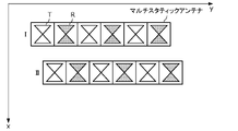
- FIG. 1 is a diagram showing a multi-static antenna in a reference example.
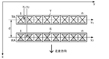
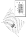
- FIG. 2 is a diagram showing an example of an S-Array multistatic antenna according to the embodiment.
- FIG. 3 is a diagram showing an example of each coordinate regarding S-Array in the embodiment.
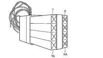
- FIG. 4 is an external view of the S-Array in the embodiment.
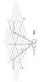
- FIG. 5 is a conceptual diagram showing a one-dimensional multi-static array antenna.
- FIG. 6 is a conceptual diagram showing the relationship between transmission points and reception points.
- FIG. 7 is a conceptual diagram showing coordinates of transmission points and reception points.
- FIG. 8 is a conceptual diagram showing the relationship between transmission points and reception points in forward scattering.
- FIG. 9 is a conceptual diagram showing the relationship between transmission points and reception points on a plane.
- FIG. 1 is a diagram showing a multi-static antenna in a reference example.
- FIG. 2 is a diagram showing an example of an S-Array multistatic antenna according to the embodiment.
- FIG. 3 is a diagram showing an
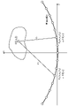
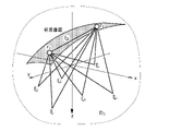
- FIG. 10 is a conceptual diagram showing the relationship between transmission points and reception points on a curved surface.
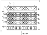
- FIG. 11 is a diagram showing a multi-row linear array antenna.
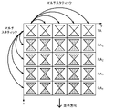
- FIG. 12 is a conceptual diagram showing combinations of transmission positions and reception positions of a multi-static array antenna.
- FIG. 13 is a diagram showing a quasi-two-dimensional array antenna on a curved surface.
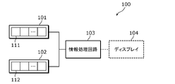
- FIG. 14 is a block diagram showing the basic configuration of the imaging device according to the embodiment.
- FIG. 15 is a flow chart showing the basic operation of the imaging device according to the embodiment.
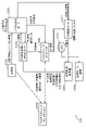
- FIG. 16 is a block diagram showing a specific configuration of the imaging device according to the embodiment.
- An imaging device includes a transmitter array including a plurality of transmitters that are arranged on a straight line and transmit waves to an area to be measured, and parallel to the straight line on which the plurality of transmitters are arranged.
- a receiver array spaced from the transmitter array including a plurality of receivers arranged in a separate line for receiving the waves from the region; and the plurality of transmitters and the plurality of receivers. and the distance between the straight line on which the plurality of transmitters are arranged and the straight line on which the plurality of receivers are arranged. and an information processing circuit for deriving a visualization function corresponding to the field function and using the visualization function to visualize the structure of the scatterers included in the object within the region.
- the imaging device can acquire sufficient information as measurement data according to various combinations of multiple transmitters in the transmitter array and multiple receivers in the receiver array.
- the imaging device since the imaging device is provided with a space between the transmitter row and the receiver row, it can properly transmit the wave to the area and receive the wave properly from the area. Then, the imaging device can appropriately visualize the structure of the scatterer using the wave measurement data and the imaging function derived according to the distance between the transmitter array and the receiver array.
- the imaging apparatus constrains the placement of the transmitter and receiver on two straight lines, it is possible to simplify arithmetic processing compared to the case where the transmitter and receiver are arbitrarily placed. Therefore, the imaging device can suppress complication of arithmetic processing. That is, the imaging device can visualize the structure of the scatterer contained in the object in the area using the wave motion, and while suppressing the complexity of the arithmetic processing, the spatial resolution in the visualization of the structure of the scatterer can be increased. can be enhanced.
- the information processing circuit derives the scattered field function according to the measurement data and the distance, derives the imaging function according to the scattered field function, and the scattered field function is and ⁇ 1 and ⁇ 2 are expressed as where (x 1 , y 1 , z) indicates the transmitting position of the wave, (x 2 , y 2 , z) indicates the receiving position of the wave, and k is the wave number of the wave where D denotes the region, ( ⁇ , ⁇ , ⁇ ) corresponds to the reflection position of the wave and ⁇ corresponds to the unknown reflectivity at the reflection position.
- the imaging device can derive a scattered field function determined on the assumption that the transmission position and the reception position have the same z-coordinate, and can derive the imaging function according to the scattered field function. .
- the imaging device appropriately scatter field functions and images according to the measured data obtained with the plurality of transmitters in the transmitter array and the plurality of receivers in the receiver array along the planar boundaries of the region. can be derived.
- the information processing circuit derives the scattered field function by solving an equation satisfied by the scattered field function, and the equation is: and ⁇ 5 is where c denotes the propagation speed of said wave and t denotes the time from transmission to reception of said wave.
- the imaging device can analytically derive the solution of the equation that the scattered field function satisfies as the scattered field function. Therefore, the imaging device can efficiently derive a suitable scattered field function.
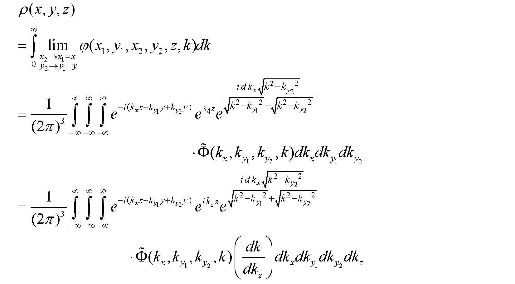
- the visualization function is and (x, y, z) indicate the imaging target position.
- the imaging device can derive the imaging function according to the limit manipulation of the scattered field function. Accordingly, the imaging device can visualize the state of scattering within the region, and can appropriately visualize the structure of the scatterers included in the object within the region.
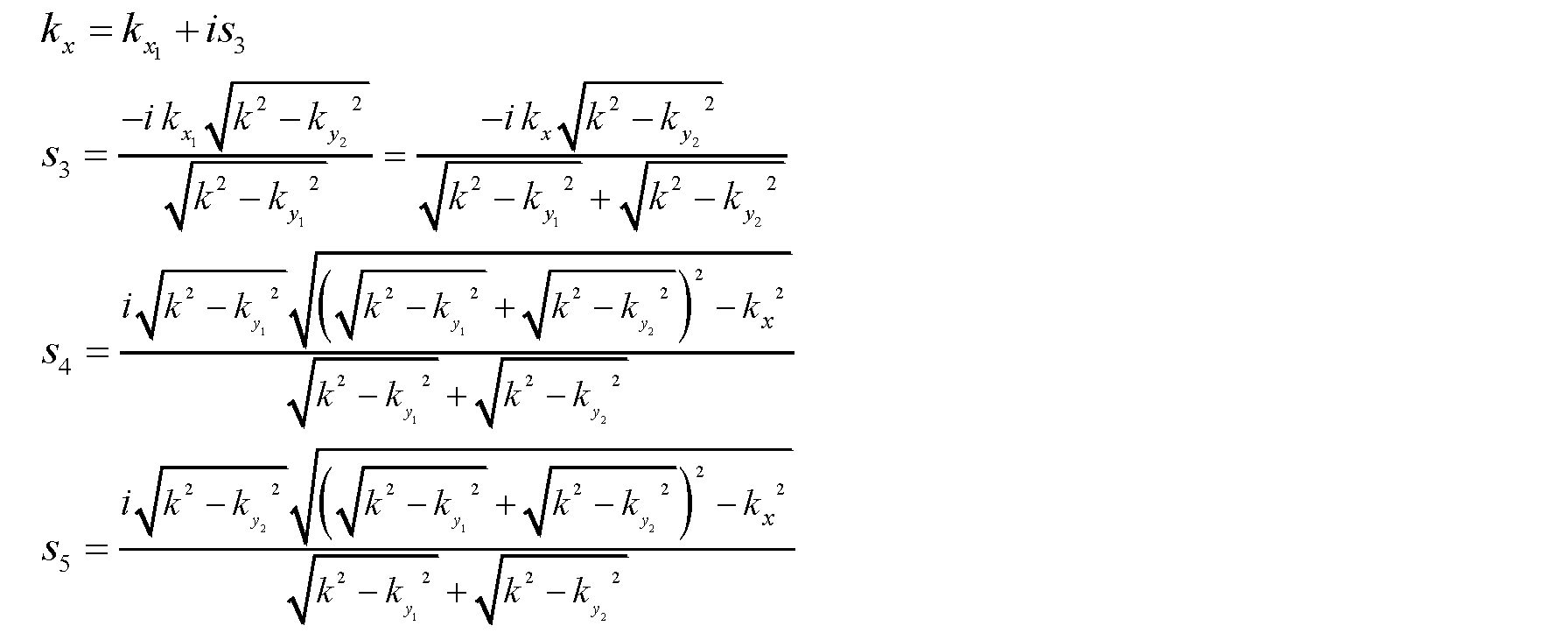
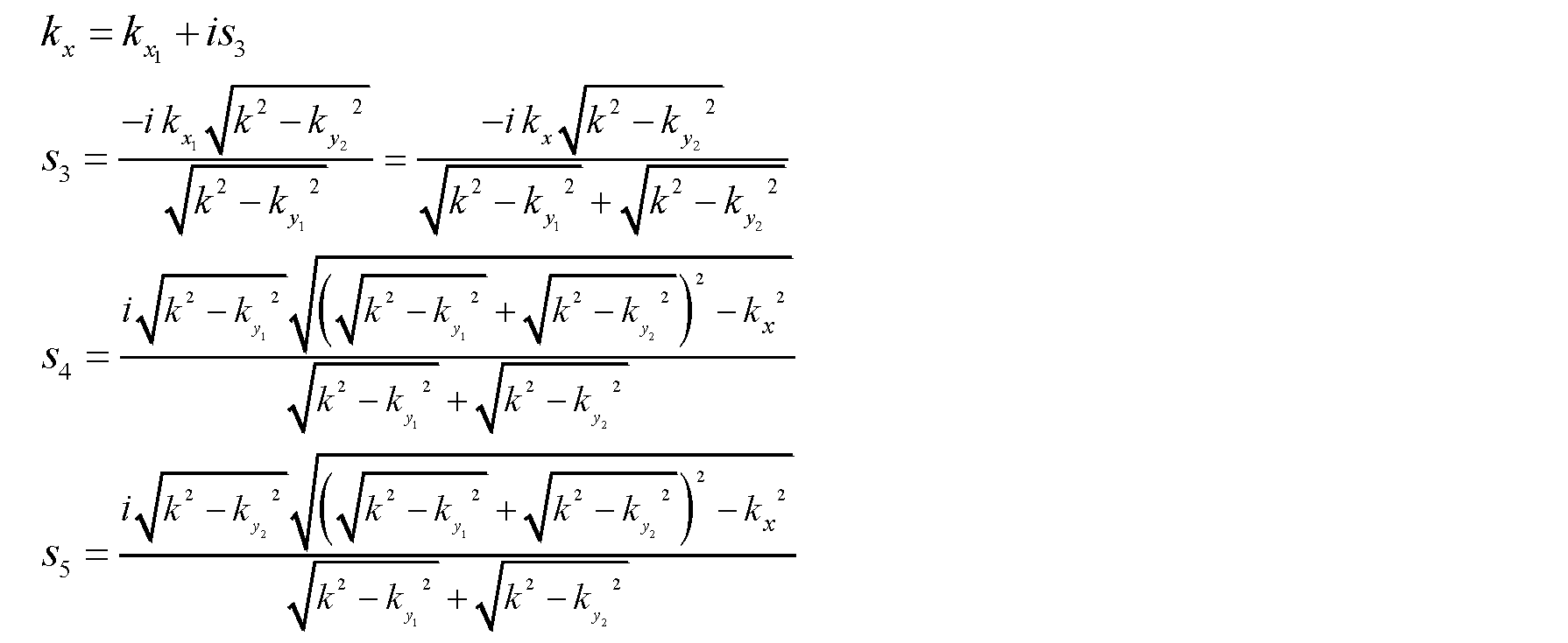
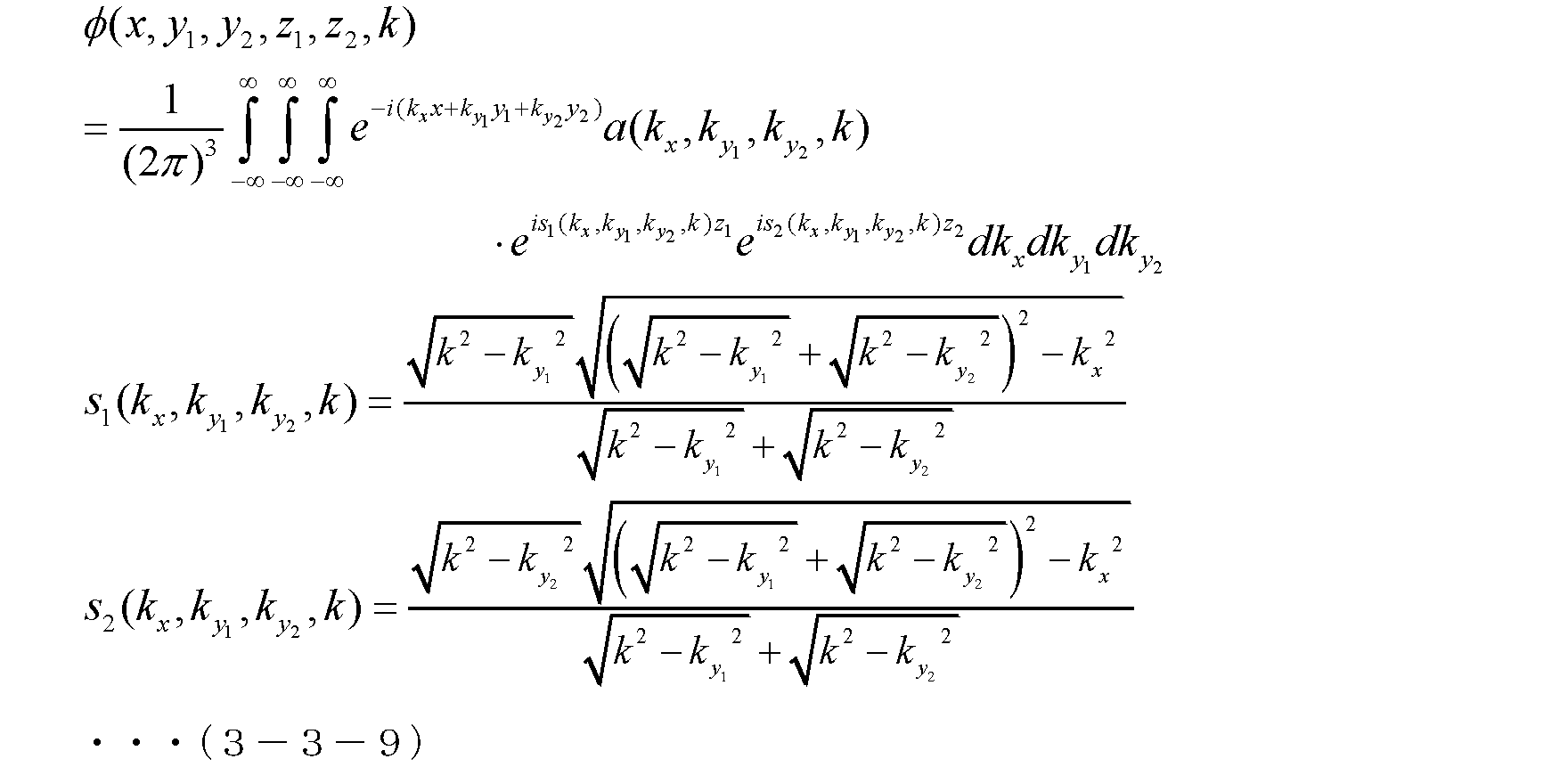
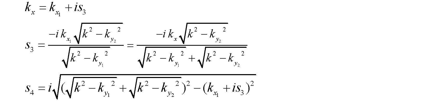
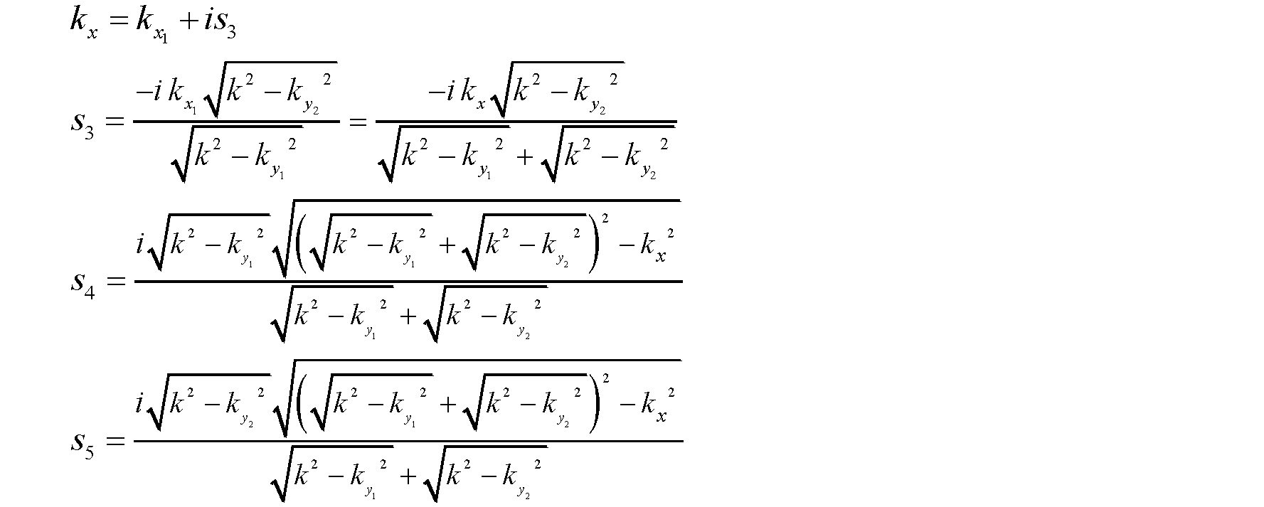
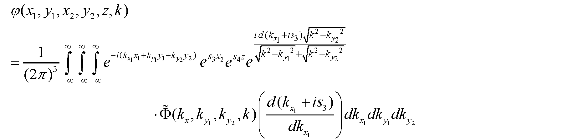
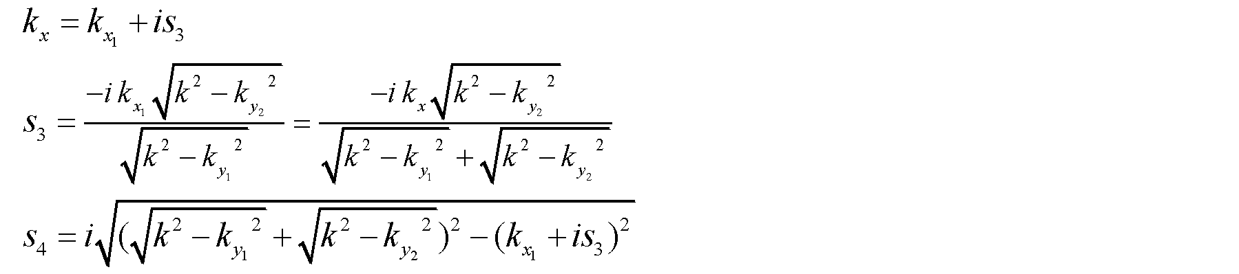
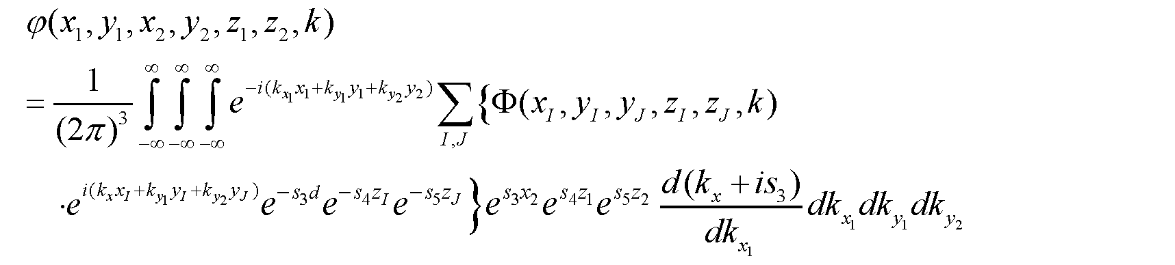
- the information processing circuit is derived as the scattered field function, and k x , s 3 and s 4 are where k x1 , k y1 and k y2 denote the wavenumbers for x 1 , y 1 and y 2 of said scattered field function, d denotes said distance, denotes the measured data Fourier transformed with respect to x 1 , y 1 and y 2 .
- the imaging device can appropriately reflect the wave measurement data and the distance between the transmitter array and the receiver array in the scattered field function. Therefore, the imaging device can derive a scattered field function that adequately represents the scattering state.
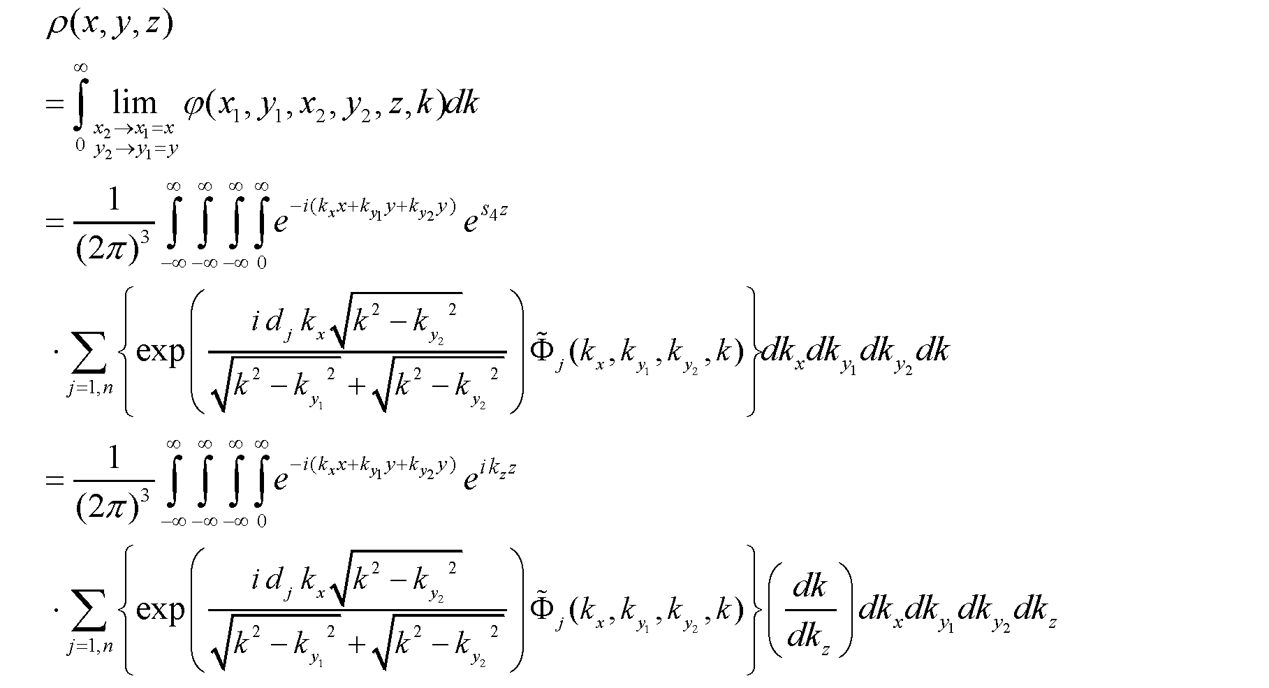
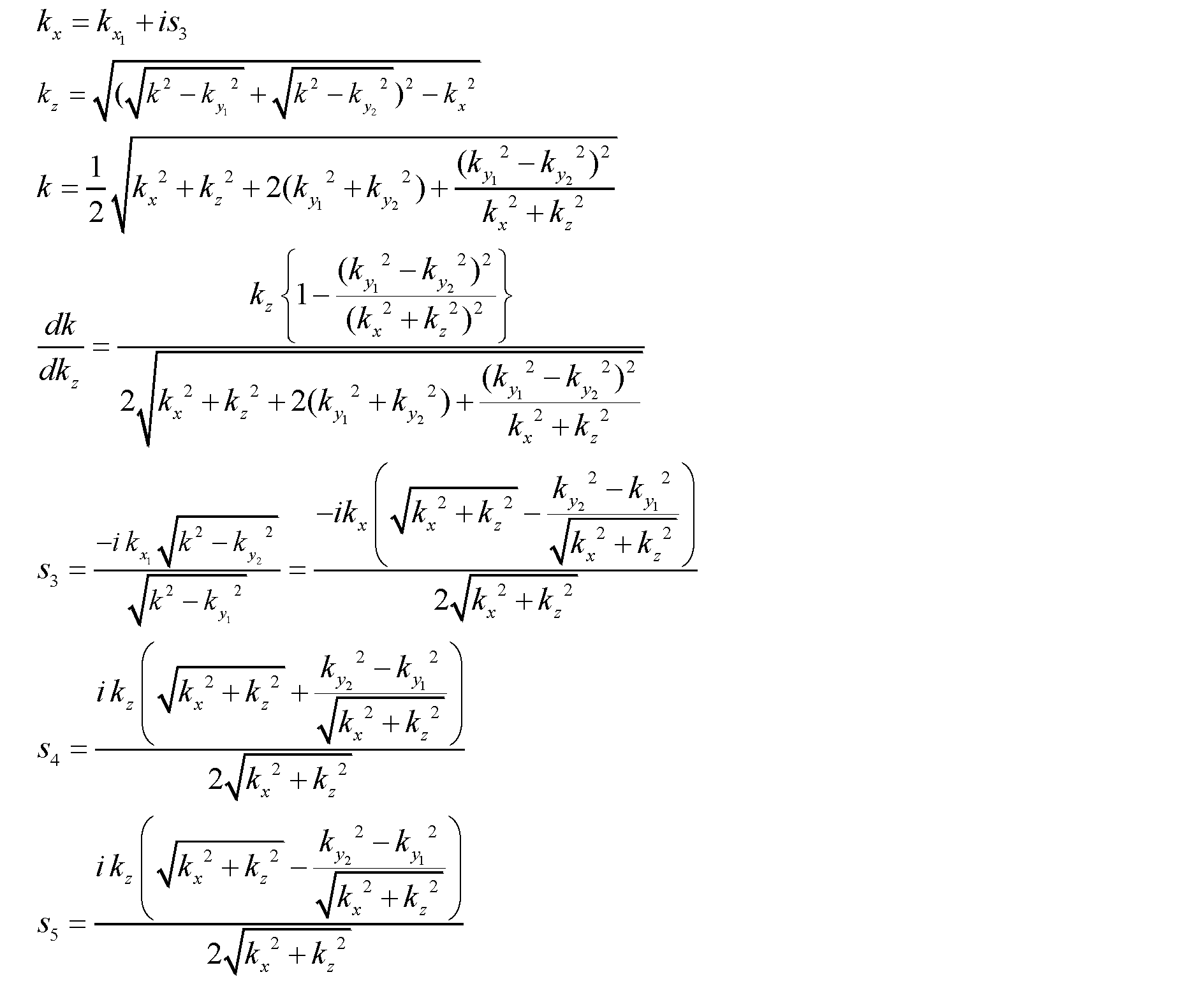
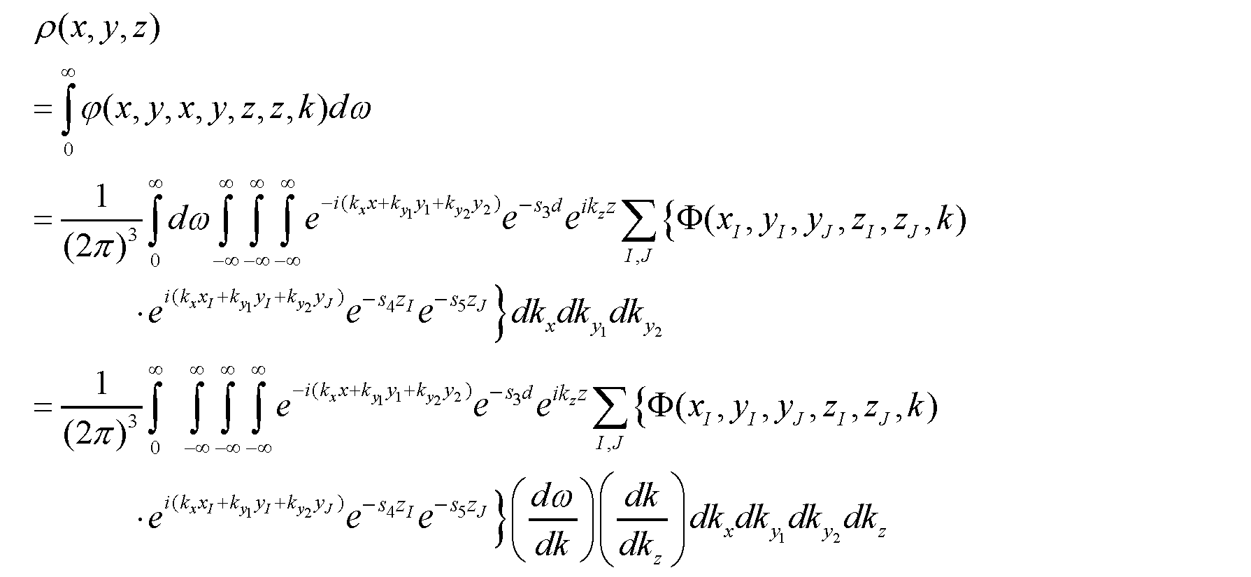
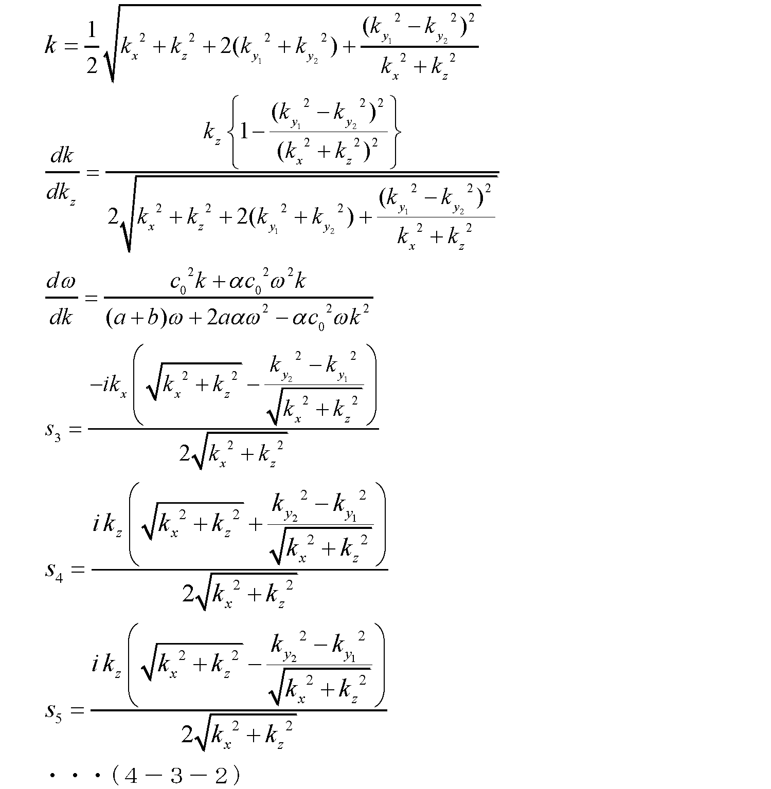
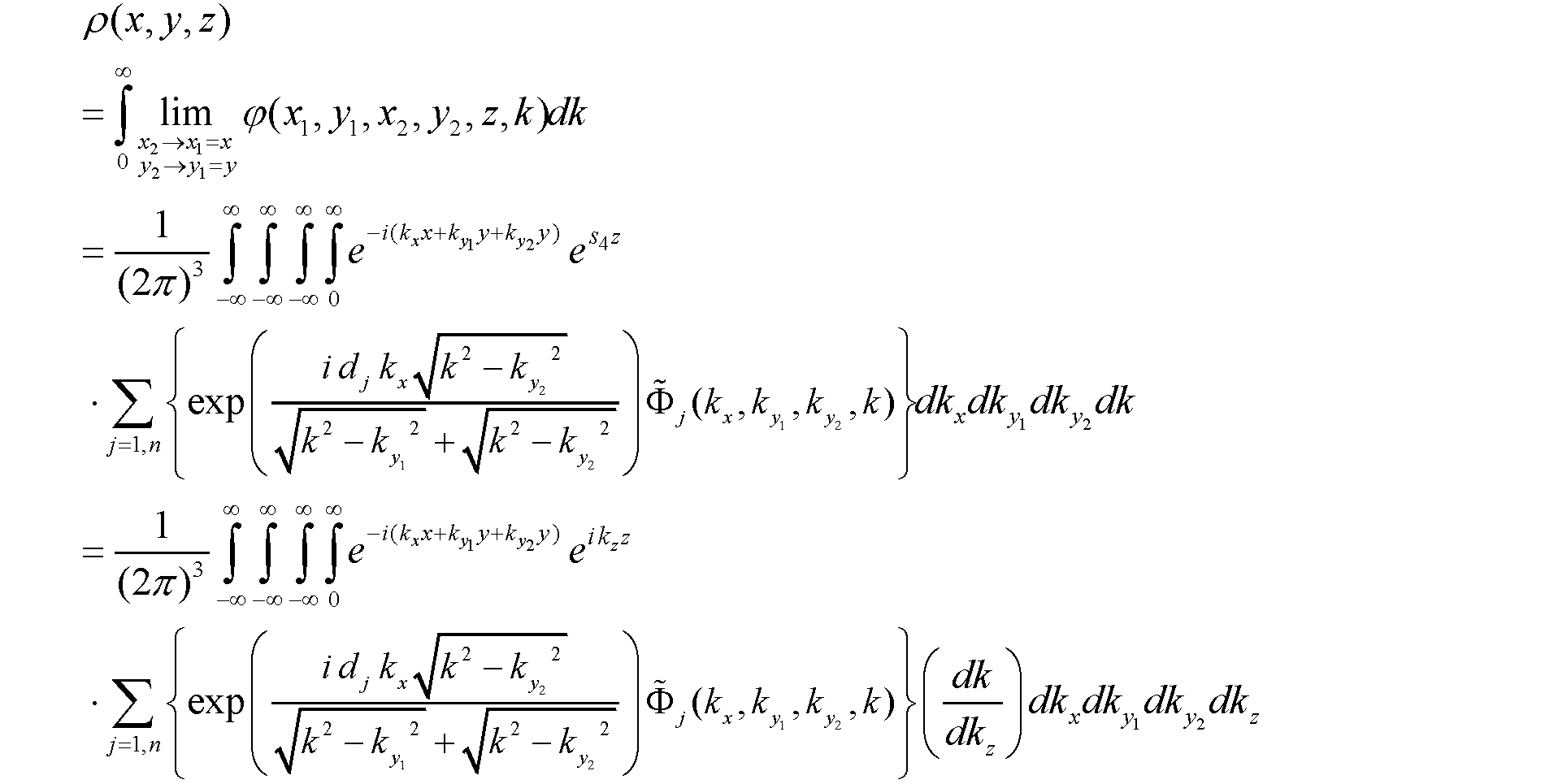
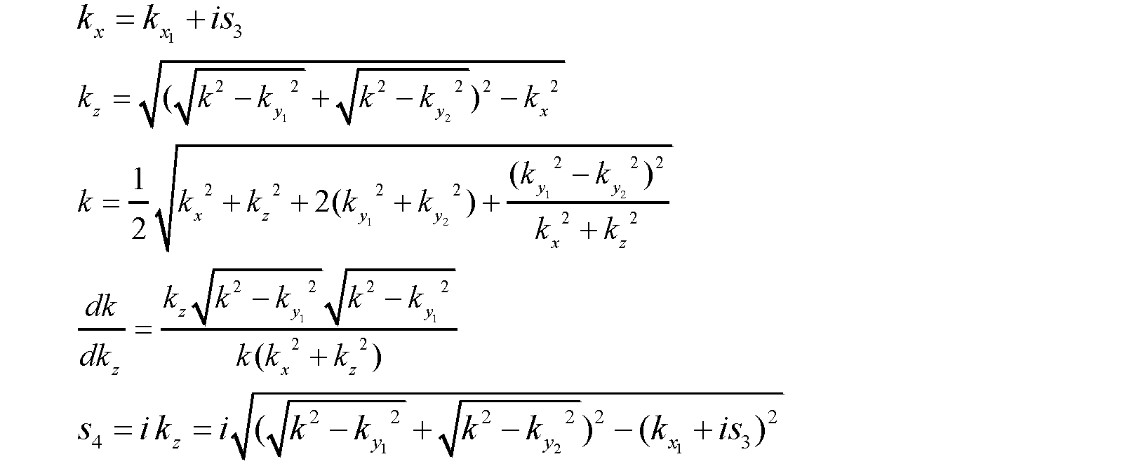
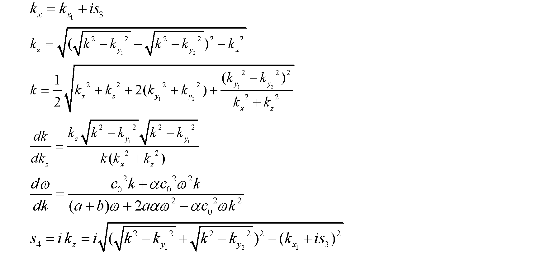
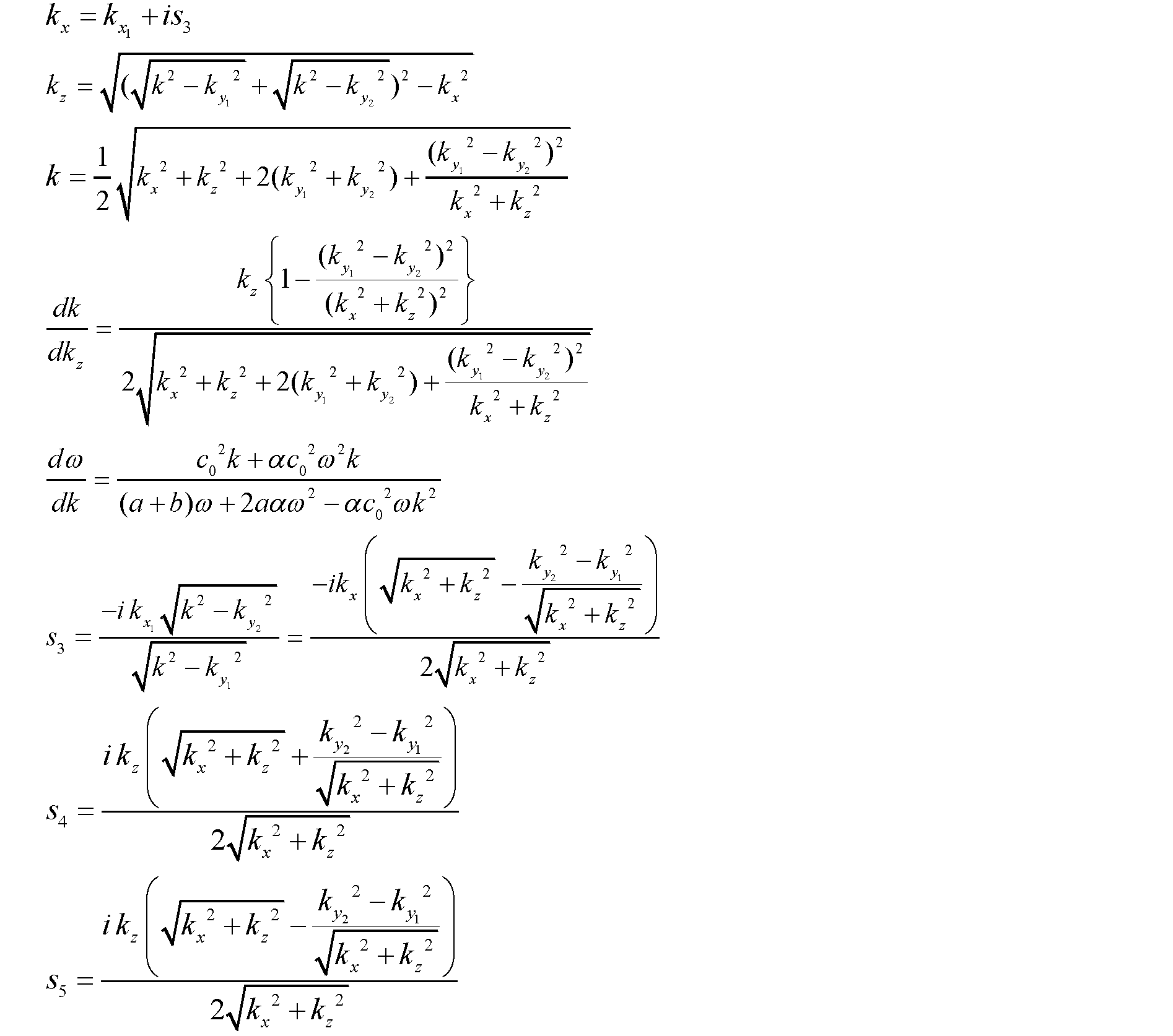
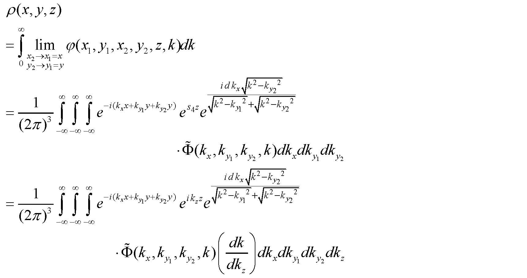
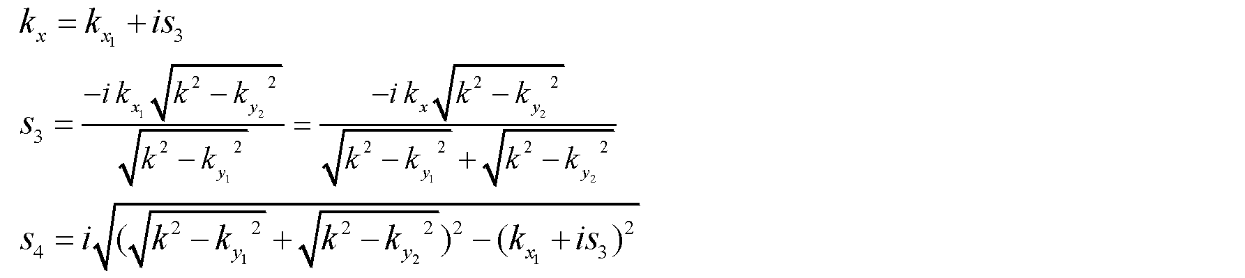
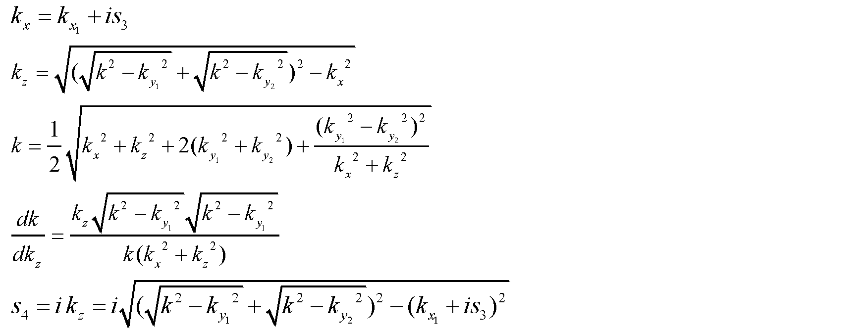
- the information processing circuit as the imaging function, and k x , k z , k, dk/dk z and s 4 are and s 3 is defined by where (x, y, z) denotes the position to be imaged, k x1 , k y1 and k y2 denote the wavenumbers for x 1 , y 1 and y 2 of the scattered field function, and d is , indicating said distance, denotes the measured data Fourier transformed with respect to x 1 , y 1 and y 2 .
- the imaging device can appropriately reflect the wave measurement data and the distance between the transmitter row and the receiver row in the imaging function.
- the imaging device can derive an imaging function that adequately represents the state of scattering.
- the imaging device may include a plurality of transmitter trains as the transmitter train, a plurality of receiver trains as the receiver train, or a plurality of transmitter trains and receiver trains as the transmitter train and the receiver train.
- a plurality of receiver trains is provided.
- the imaging device can acquire sufficient information as measurement data according to multiple combinations of transmitter trains and receiver trains. Also, the imaging device can establish a multi-static relationship in two directions, parallel and orthogonal to the transmitter and receiver rows. Therefore, the imaging device can properly visualize the structure of the scatterers included in the object within the region.
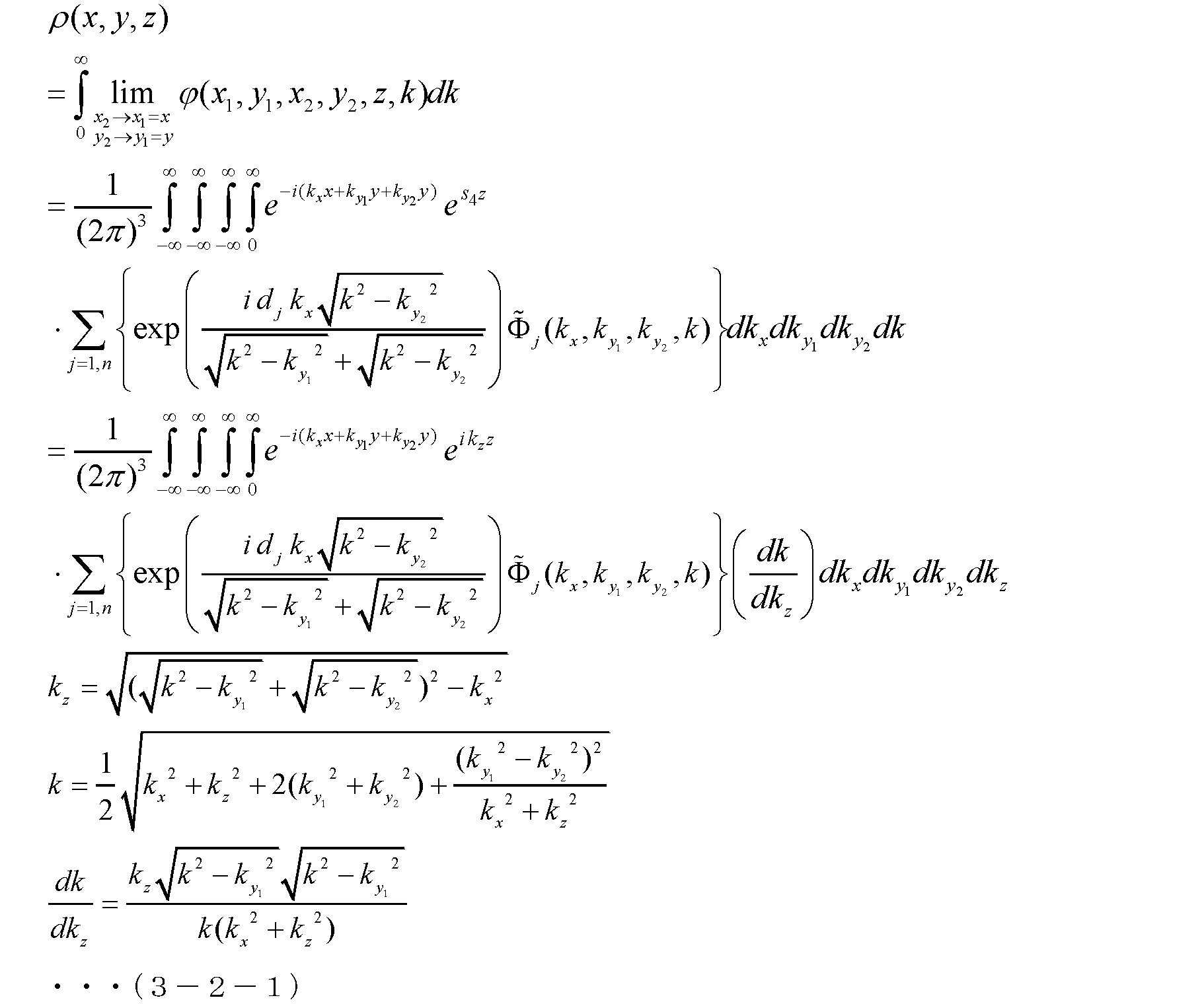
- the information processing circuit for one transmitter row and n receiver rows provided as the transmitter row and the receiver row of the imaging device, as the imaging function, and k x , k z , k, dk/dk z and s 4 are and s 3 is defined by where (x, y, z) denotes the position to be imaged, k x1 , k y1 and k y2 denote the wavenumbers for x 1 , y 1 and y 2 of the scattered field function, and d j indicates the distance, denotes the measured data Fourier transformed with respect to x 1 , y 1 and y 2 .
- the imaging device can appropriately reflect the wave measurement data and the distance between the transmitter row and the receiver row in the imaging function. Specifically, the imaging device performs linear addition corresponding to the distance between the transmitter row and the receiver row to the measurement data obtained according to a plurality of combinations of the transmitter row and the receiver row. , we can derive an imaging function that adequately describes the scattering state.
- the information processing circuit as the imaging function
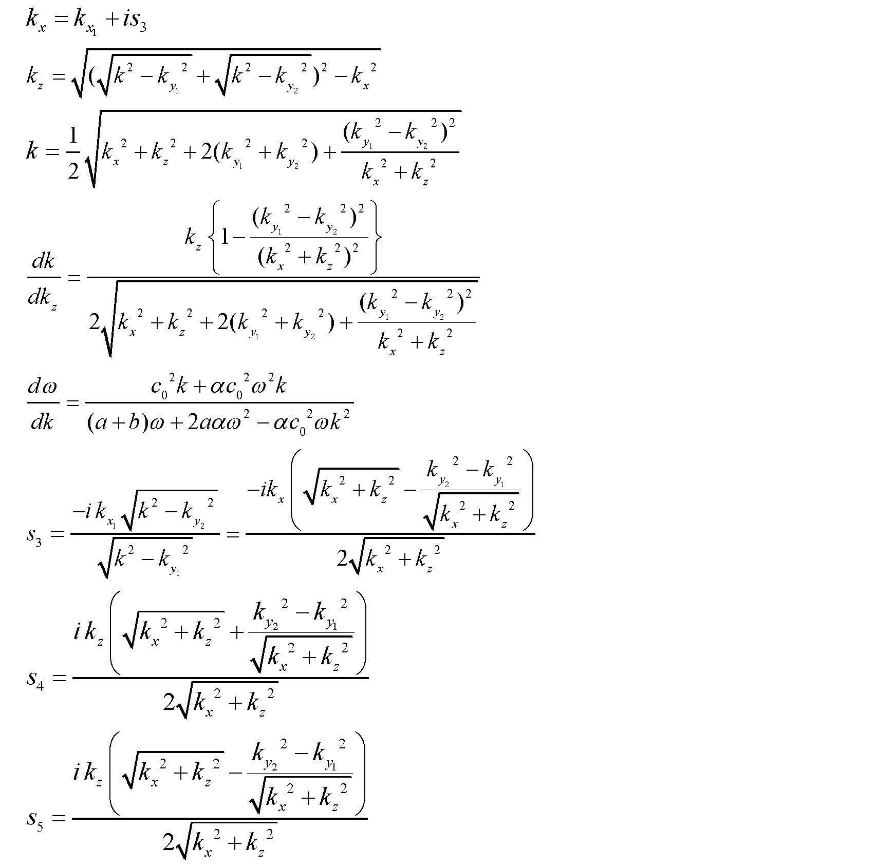
- k x , k z , k, dk/dk z , d ⁇ /dk and s 4 are: and s 3 is defined by where (x, y, z) denotes the position to be imaged
- k x1 , k y1 and k y2 denote the wavenumbers for x 1 , y 1 and y 2 of the scattered field function
- d is , denotes the distance
- ⁇ denotes the angular frequency of the wave
- c 0 denotes the propagation velocity of the wave in vacuum
- a, b and ⁇ denotes the parameters for Debye relaxation, denotes the measured data Fourier transformed with respect to x 1 , y 1 and y 2 .
- the visualization device can derive a visualization function that reflects parameters related to Debye relaxation. Therefore, the imaging device can suppress accuracy deterioration that occurs depending on the wave frequency.
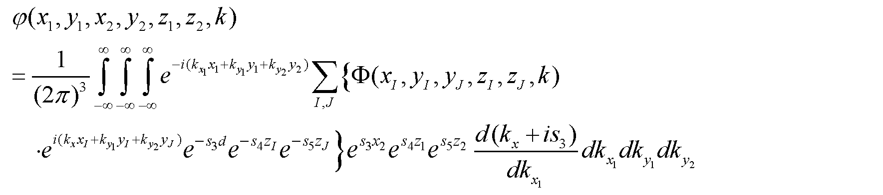
- the information processing circuit derives the scattered field function according to the measurement data and the distance, derives the imaging function according to the scattered field function, and the scattered field function is and ⁇ 1 and ⁇ 2 are expressed as where (x 1 , y 1 , z 1 ) indicates the transmitting position of the wave, (x 2 , y 2 , z 2 ) indicates the receiving position of the wave, and k is the wave Denoting the wave number, D denoting the area, ( ⁇ , ⁇ , ⁇ ) corresponding to the reflection position of the wave, and ⁇ corresponding to the unknown reflectivity at the reflection position.
- the imaging device to derive a scattered field function defined on the assumption that the transmit and receive positions may have different z-coordinates, and derive the imaging function according to the scattered field function.
- the imaging device suitably scatters along the tangent plane of the region with curved boundaries according to the measurement data obtained with the plurality of transmitters in the transmitter array and the plurality of receivers in the receiver array.
- a field function and an imaging function can be derived.
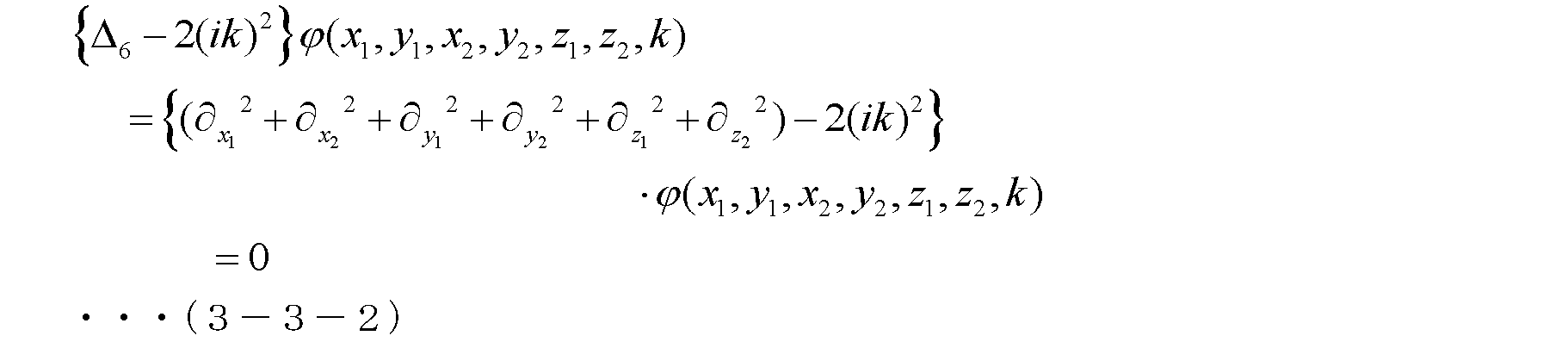
- the information processing circuit derives the scattered field function by solving an equation satisfied by the scattered field function, and the equation is: and ⁇ 6 is Determined by
- the imaging device can analytically derive the solution of the equation that the scattered field function satisfies as the scattered field function. Therefore, the imaging device can efficiently derive a suitable scattered field function.
- the visualization function is and (x, y, z) indicate the imaging target position.
- the imaging device can derive the imaging function using the scattered field function to which the imaging target position is input. Accordingly, the imaging device can visualize the state of scattering within the region, and can appropriately visualize the structure of the scatterers included in the object within the region.
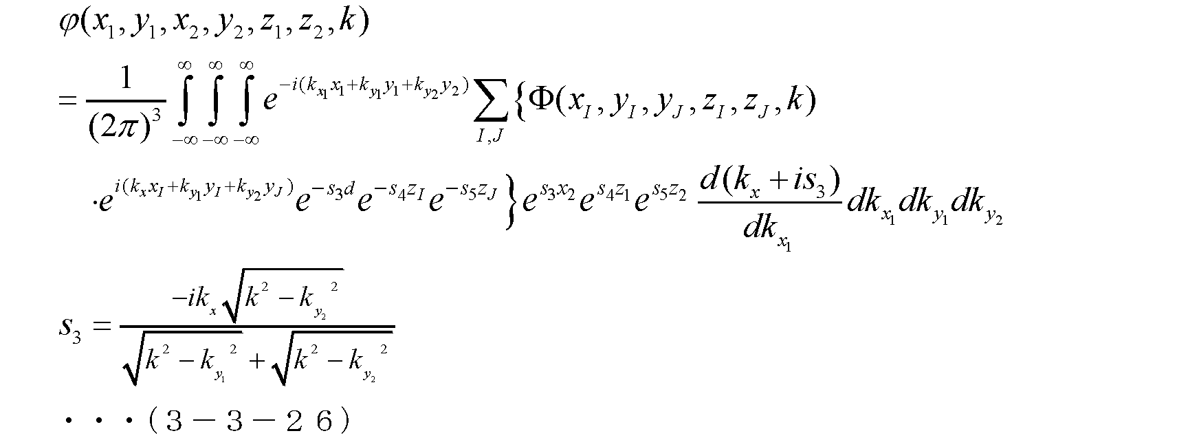
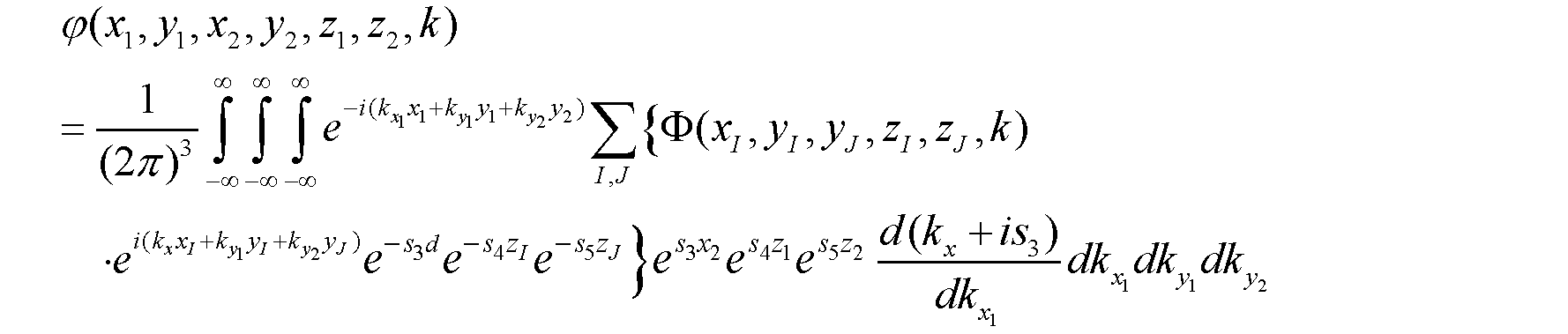
- the information processing circuit is derived as the scattered field function, and k x , s 3 , s 4 and s 5 are where k x1 , k y1 and k y2 denote the wavenumbers for x 1 , y 1 and y 2 of the scattered field function, d denotes the distance, and ⁇ (x I , y I , y J , zI , zJ , k) indicates the measurement data when the transmission position is ( xI , yI , zI ) and the reception position is ( xI + d, yJ , zJ ). .
- the imaging device can appropriately reflect the wave measurement data and the distance between the transmitter array and the receiver array in the scattered field function. Therefore, the imaging device can derive a scattered field function that adequately represents the scattering state.
- the information processing circuit as the imaging function, and k x , k z , k, dk/dk z , s 3 , s 4 and s 5 are: where (x, y, z) denotes the position to be imaged, k x1 , k y1 and k y2 denote the wavenumbers for x 1 , y 1 and y 2 of the scattered field function, and d is , indicates the distance, and ⁇ (x I , y I , y J , z I , z J , k) indicates that the transmission position is (x I , y I , z I ) and the reception position is (x I +d , y J , z J ).
- the imaging device can appropriately reflect the wave measurement data and the distance between the transmitter row and the receiver row in the imaging function.
- the imaging device can derive an imaging function that adequately represents the state of scattering.
- the information processing circuit derives the imaging function using a synthesis of a plurality of scattered field functions for a plurality of combinations of the transmitter array and the receiver array, and calculates each of the plurality of scattered field functions corresponds to the scattered field function, where k x , s 3 , s 4 and s 5 are where k x1 , k y1 and k y2 denote the wavenumbers for x 1 , y 1 and y 2 of the scattered field function, d denotes the distance, and ⁇ (x I , y I , y J , zI , zJ , k) indicates the measurement data when the transmission position is ( xI , yI , zI ) and the reception position is ( xI + d, yJ , zJ ). .
- the imaging device appropriately expresses the state of scattering by synthesizing the measurement data of the waves and a plurality of scattered field functions that reflect the distance between the transmitter array and the receiver array. can be derived.
- the information processing circuit is derived as the imaging function
- k x , k z , k, dk/dk z , d ⁇ /dk, s 3 , s 4 and s 5 are: where (x, y, z) denotes the position to be imaged, k x1 , k y1 and k y2 denote the wavenumbers for x 1 , y 1 and y 2 of the scattered field function, and d is , denotes the distance, ⁇ denotes the angular frequency of the wave, c 0 denotes the propagation velocity of the wave in vacuum, a, b and ⁇ denotes the parameters for Debye relaxation, denotes the measured data Fourier transformed with respect to x 1 , y 1 and y 2 .
- the visualization device can derive a visualization function that reflects parameters related to Debye relaxation. Therefore, the imaging device can suppress accuracy deterioration that occurs depending on the wave frequency.
- a visualization method includes the steps of: transmitting waves to a measurement target area by the plurality of transmitters in a transmitter array including a plurality of transmitters arranged in a straight line; said plurality of receivers in a row of receivers spaced from said row of transmitters comprising a plurality of receivers arranged on another straight line parallel to the straight line on which said plurality of transmitters are arranged; a step of receiving the waves from the transmitter, measurement data obtained by a combination of all or part of the plurality of transmitters and the plurality of receivers, and a straight line on which the plurality of transmitters are arranged and the plurality of Deriving an imaging function corresponding to the scattered field function for the scattering of the wave according to the distance between the receiver and the straight line, and using the imaging function to detect scatterers contained in objects in the region and visualizing the structure of
- the imaging device uses waves to visualize the structure of scatterers contained in objects within a region.
- the imaging apparatus will be described in detail, including its underlying technology and theory.
- This disclosure describes microwave imaging techniques based on super-array (S-Array) scattering field theory.
- FIG. 1 is a diagram showing a multistatic (MS) antenna in a reference example.
- a multistatic (MS) antenna In the multistatic antenna, a plurality of transmitting antenna elements T and a plurality of receiving antenna elements R are alternately arranged in a line.
- the transmit antenna elements T and receive antenna elements R may also be simply referred to as transmit elements and receive elements.
- Each antenna element is half-wavelength ( ⁇ /2) in size. Therefore, the resolution in the y-axis direction is half a wavelength ( ⁇ /2). Since this does not satisfy the Nyquist sampling condition, a phenomenon called aliasing occurs. To this end, it is conceivable to scan in the x direction by shifting the antenna array by ⁇ /4 in the y direction. Alternatively, a method of bundling two independent array antenna systems from the beginning and scanning them together is also used.
- the data obtained with the multistatic antenna in FIG. 1 are 9 pairs at positions I and II of the multistatic antenna, for a total of 18 pairs. Furthermore, the data obtained when coupling due to electromagnetic induction between adjacent transmitting/receiving elements is eliminated is 4 pairs for each of I and II, for a total of only 8 pairs. It is difficult to realize a single array antenna system that satisfies the Nyquist sampling theorem for any arrangement of antenna elements.
- FIG. 2 is a diagram showing an example of an S-Array multistatic antenna according to this embodiment.
- An S-Array multi-static antenna may be simply referred to as an S-Array.
- the S-Array multi-static array antenna includes two rows of array antennas, a transmit array antenna TA and a receive array antenna RA.
- the S-Array multi-static array antenna provides 36 pairs of data for transmission and reception.
- the S-Array scattering field theory in the present disclosure solves this problem and realizes a virtual high-density S-Array like the lower part of FIG. 2 that satisfies the Nyquist sampling condition.
- two array antennas of the transmitting array antenna TA and the receiving array antenna RA are theoretically converted into one array of transmitting and receiving array antennas. Therefore, a resolution of ⁇ /4 is obtained in the y direction. Also, scanning in the x-direction provides arbitrary resolution in the x-direction.
- the S-Array scattered field theory in the present disclosure is decisively different from existing scattered field theories for two-dimensional array antennas in the following points.
- n is the number of samples in the x direction, for example n is 128-256. Therefore, it is difficult to put existing scattered field analysis methods for two-dimensional array antennas into practical use with current computer capabilities.
- a signal is transmitted from an arbitrary element in a planar grid-like two-dimensional array antenna, and a signal is received by another arbitrary element in the two-dimensional array antenna.
- data of n 4 sets are obtained.
- Each set of data is time-series data with a band of 10 GHz or higher.
- a reconstruction theory has already been derived for an algorithm for reconstructing an image of an object from such two-dimensional multistatic data.
- imaging using this two-dimensional array antenna is not necessarily realistic due to the complexity of the device and the difficulty of obtaining effective resolution.
- the S-Array scattering field theory is very sophisticated as described below, and the scattering inverse analysis algorithm can be obtained with a slight change from the existing one-dimensional algorithm, so the feasibility is very high. expensive.
- FIG. 3 is a diagram showing an example of each coordinate related to the S-Array in this embodiment.
- the S-Array is a quasi-two-dimensional array antenna composed of two linear array antennas, one row of transmission array antenna TA and one row of reception array antenna RA, as shown in FIG.
- the transmit array antenna TA includes n transmit antenna elements T.
- the receive array antenna RA includes n receive antenna elements R.
- the x coordinate of the transmitting array antenna TA is represented by x1
- the x coordinate of the receiving array antenna RA is represented by x2
- the distance in the x direction between the transmitting array antenna TA and the receiving array antenna RA is represented by d. be.
- n2 pieces of time - series data of arbitrary combinations of n transmitting elements and n receiving elements are obtained at each point x in the scanning direction.
- FIG. 4 is an external view of the S-Array in this embodiment.
- a transmitting array antenna TA including a plurality of transmitting antenna elements T and a receiving array antenna RA including a plurality of receiving antenna elements R are configured separately. That is, a plurality of transmitting antenna elements T and a plurality of receiving antenna elements R are arranged in a quasi-two-dimensional manner.
- k represents the wave number.
- ⁇ represents the Laplace operator.
- ⁇ represents the partial derivative of the variable indicated by the suffix.
- This method is called monostatic. In this method, pairs of integrated transmitting and receiving elements are arranged along the y-axis. If there are n paired elements for transmission and reception, n sets of data can be obtained. However, the accuracy obtained with this method is essentially twice the size of each antenna element for transmission and reception. Therefore, it is difficult to obtain high resolution images.
- FIG. 5 is a conceptual diagram showing a one-dimensional multi-static array antenna. As shown in FIG. 5, if any two of n elements are selected as transmitting and receiving elements, the spatial resolution is doubled. Furthermore, signals can be received with a high S/N ratio from a short distance to a long distance. The quality of the final image is thus greatly improved. Naturally, the amount of data increases by n times, but the time required for reconstruction can be dramatically shortened according to the theory described below.
- radio waves emitted from point P 1 (x, y 1 , z) are reflected at point P ( ⁇ , ⁇ , ⁇ ) and received at point P 2 (x, y 2 , z). situations are considered here.
- the signal received at P2 is represented by the following equation (2-1-2).
- ⁇ ( ⁇ , ⁇ , ⁇ ) indicates a function of the permittivity of the point P( ⁇ , ⁇ , ⁇ ) and corresponds to the reflectance at the point P( ⁇ , ⁇ , ⁇ ).
- a point P ( ⁇ , ⁇ , ⁇ ) corresponds to a reflection point.
- ⁇ ( ⁇ , ⁇ , ⁇ ) is unknown. It is also assumed that the time factor is proportional to exp(-i ⁇ t).
- the kernel function in the integrand of the above equation is expressed by ⁇ in the following equation (2-1-3).
- equation (2-1-3) has an asymptotic solution at short wavelengths (high frequencies or k is large). Solutions to such partial differential equations can be considered almost exact solutions for imaging with microwaves.
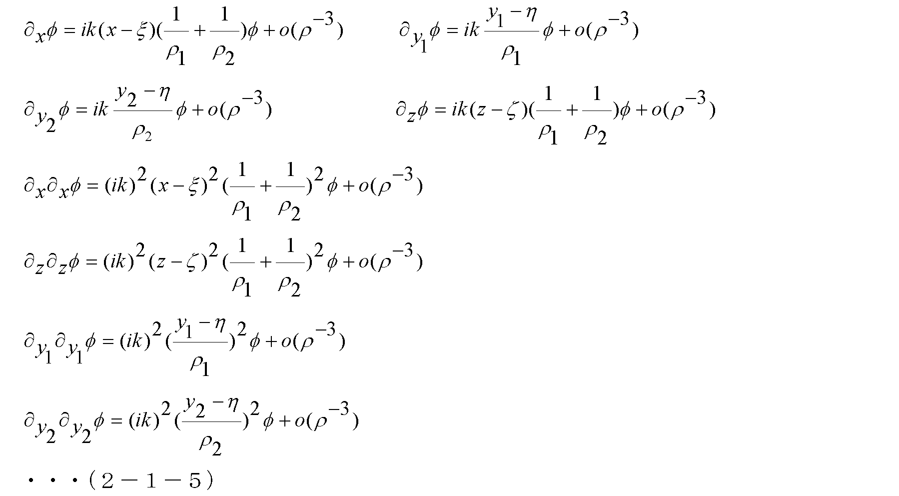
- the differential result of each order of ⁇ is expressed as in the following equation (2-1-5).
- Equation (2-1-11) is a partial differential equation whose solution is ⁇ in equation (2-1-3).
- equation (2-1-2) By applying differentiation to the integral kernel of equation (2-1-2), of equation (2-1-2) also satisfies the above partial differential equation.
- This equation is a four-dimensional pseudo-wave equation consisting of five variables (t, x, y 1 , y 2 , z).
- FIG. 6 is a conceptual diagram showing the relationship between transmission points and reception points.
- FIG. 6 shows the situation in which the wave from r 1 is reflected at points ⁇ ( ⁇ 1 , ⁇ 2 , . . . ) and returns to point r 2 .
- the wave transmission point r 1 and wave reception point r 2 move independently and freely within the x-section D while satisfying certain constraint conditions.
- this function G(r 1 , r 2 , ⁇ ) should be related to the distribution of reflection points in the region. is.
- G(r 1 , r 2 , ⁇ ) is the sum of reflected signals from all points ⁇ . Also, since there are many reflection points in the area, G(r 1 , r 2 , ⁇ ) can be expressed as in the following equation (2-2-1).
- the constraint imposed on the wave transmission point r1 and the wave reception point r2 is that the x - coordinates of r1 and r2 are always equal.
- the function G(r 1 , r 2 , ⁇ ) will be used below to explain the theoretical structure of the inverse scattering problem. Also, here, a partial area of the three-dimensional space is expressed as D, and its boundary is expressed as ⁇ D. In this case, the function G(r 1 , r 2 , ⁇ ) becomes the solution of the differential equation inside the region D as shown in the following equation (2-2-2).
- Tr indicates a trace operation.
- This ⁇ (r) is a function related to the gradient of the permittivity in the region D to be obtained. Actually, it is difficult to find the differential operator L ( ⁇ / ⁇ t, ⁇ / ⁇ r 1 , ⁇ / ⁇ r 2 ) appearing here.
- FIG. 7 is a conceptual diagram showing coordinates of transmission points and reception points.
- the transmitting point is located at P 1 (x, y 1 , z 1 ) and the receiving point is located at P 2 (x, y 2 , z 2 ).
- a wave radiated from the transmitting point P1 is reflected at the point P ( ⁇ , ⁇ , ⁇ ) and reaches the receiving point P2.
- z 1 and z 2 are arbitrary.
- the measurement points corresponding to the transmission point P1 and the reception point P2 move on the cross - sectional curve S.
- the distance between P1 and P is expressed by ⁇ 1
- the distance between P2 and P is expressed by ⁇ 2 .
- ⁇ ( ⁇ , ⁇ , ⁇ ) denotes a function of the permittivity of the point ( ⁇ , ⁇ , ⁇ ) and corresponds to the reflectance at the point ( ⁇ , ⁇ , ⁇ ).
- a point ( ⁇ , ⁇ , ⁇ ) corresponds to a reflection point.
- ⁇ ( ⁇ , ⁇ , ⁇ ) is unknown.
- k indicates a wave number. It is also assumed that the time factor is proportional to exp(-i ⁇ t).
- the function in the integrand of the above formula (2-2-5) is the formula (2-2-1) is. That is, the following formula (2-2-6) holds.
- equation (2-2-6) is an asymptotic solution at high frequencies. Therefore, the calculation is performed while ignoring higher-order terms with respect to 1/ ⁇ generated in the differentiation result.
- abbreviated notation of differentiation is defined as in the following equation (2-2-7).
- equation (2-2-10) is considered, assuming that the time factor of ⁇ is proportional to exp(-i ⁇ t).
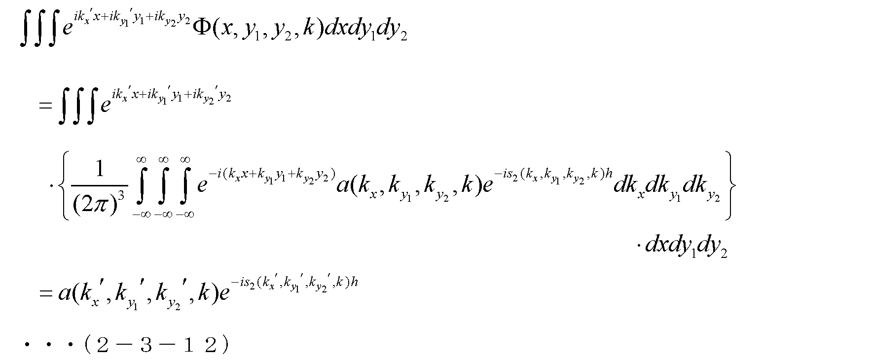
- equation (2-2-11) is obtained by subjecting ⁇ to multiple Fourier transform with respect to t, x, y 1 and y 2 .
- FIG. 8 is a conceptual diagram showing the relationship between transmission points and reception points in forward scattering.
- Forward scattering differs from backward scattering (II- 2 ) in that the z-coordinates of all scattering points are between the z - coordinates of transmitting point r1 and receiving point r2.
- Scattering data are measured by moving freely under the constraint that r1 and r2 are located at the same x - coordinate on ⁇ D1 and ⁇ D2 , respectively .
- the scattered field function in this system is defined by the following equation (2-3-1).
- Equation (2-2-5) for the backscatter example is that the phase factor of exp(-ik ⁇ 2 )/ ⁇ 2 in the integral symbol is negative.
- the scattered field function satisfies the partial differential equation of the following equation (2-3-2), which is the same as equation (2-2-10) in the backscattering example.
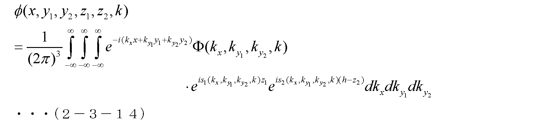
- equation (2-3-2) the solution of equation (2-3-2) is considered, assuming that the time factor of ⁇ is proportional to exp(-i ⁇ t).
- equation (2-3-2) the solution of equation (2-3-2) is considered, assuming that the time factor of ⁇ is proportional to exp(-i ⁇ t).
- the following equation is obtained by subjecting ⁇ to multiple Fourier transform with respect to t, x, y 1 and y 2 .
- FIG. 9 is a conceptual diagram showing the relationship between transmission points and reception points on a plane.
- microwaves emitted from point P1 are reflected at point P on the target and received at point P2.
- the points P1 and P2 move to arbitrary points on the grid points ( two -dimensional antenna array) in the plane.
- a method for processing such complex data to obtain an image is described below.
- a radio wave emitted from a point P 1 (x 1 , y 1 , z) is reflected at a point P ( ⁇ , ⁇ , ⁇ ), and a point P 2 (x 2 , y 2 , z ).
- the signal received at P2 as point P moves through region D is expressed as:
- Equation (2-4-2) a partial differential equation in which this formula (2-4-2) is an asymptotic solution at short wavelengths is examined. Therefore, the calculation is performed while ignoring higher-order terms with respect to 1/ ⁇ generated in the differentiation result.
- the abbreviated notation of differentiation is defined as shown in Equation (2-4-3).
- Equation (2-4-10) is a partial differential equation whose solution is the kernel function shown in equation (2-4-2).
- ⁇ also satisfies the above partial differential equation.
- This equation is a five-dimensional pseudo-wave equation consisting of six variables (t, x 1 , y 1 , x 2 , y 2 , z).
- ⁇ can be obtained by the following formula (2-4-16).
- equation (2-4-18) is obtained as an imaging function by integrating equation (2-4-17) with respect to k.
- Equation (2-4-18) The integrals of k x1 , k y1 , k x2 and k y2 in equation (2-4-18) are in the form of Fourier transform and are suitable for computer processing.
- the exp(iz%) term in the integrand is not in Fourier transform form. So, for example, the usual integration is performed over k while specifying the value of z.
- equation (2-4-18) may be modified so that the whole is represented only by Fourier transform.
- the following formula (2-4-21) is obtained by solving each square root from the two formulas (2-4-19) and (2-4-20).
- k is expressed as in the following equation (2-4-22).
- equation (2-4-23) is obtained by differentiating both sides of equation (2-4-19) with respect to k and u.
- FIG. 10 is a conceptual diagram showing the relationship between transmission points and reception points on a curved surface.
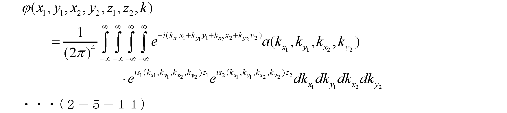
- the z-coordinates of the transmitting and receiving points are assumed to be different. Therefore, the scattered field function is expressed by the following equation (2-5-1).
- k indicates the wave number.
- the time factor is assumed to be proportional to exp(-i ⁇ t).
- D indicates a region and corresponds to D3 in FIG.
- the kernel function of the integrand in the above equation is expressed by the following equation (2-5-2).
- equation of the curved surface S is assumed as, for example, the following equation (2-5-12).
- Equation (2-5-13) is used to determine a(k x1 , k x2 , k y1 , k y2 ).
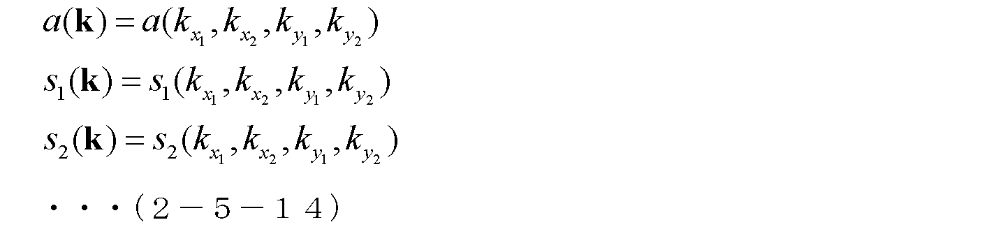
- Equation (2-5-14) is used.
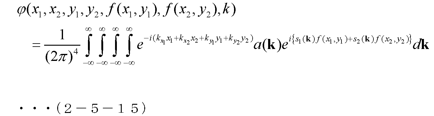
- the scattered field function can be expressed as the following formula (2-5-16).
- variable x2 may be expressed as u.
- equation (3-1-3) is obtained by Fourier transforming both sides of equation (3-1-1) with respect to t, x 1 , y 1 and y 2 .
- s 3 and s 4 are functions related to k x1 , k y1 , k y2 and k, such as the following equation (3-1-5).
- s 3 and s 4 are constants defined by k x1 , k y1 , k y2 and k.
- equation (3-1-4) is changed to the following equation (3-1-7).
- kx is expressed by the following equation (3-1-10).
- s 3 and s 4 are analytically determined according to equations (3-1-12) and (3-1-16) obtained in the above process. Then, the scattered field function is obtained from the equation (3-1-8) as shown in the following equation (3-1-17).
- ⁇ (x 1 , y 1 , y 2 , k) is the measurement data of the transmission point (x 1 , y 1 , 0), reception point (x 1 +d, y 2 , 0) and wave number k .
- Equation (3-1-20) is obtained by Fourier transforming both sides of equation (3-1-18) with respect to x 1 , y 1 and y 2 .
- a function a(k x , k y1 , k y2 , k) is obtained from the equation (3-1-20) as shown in the following equation (3-1-21).
- equation (3-1-17) which is the scattered field function, can be obtained in a complete form as in equation (3-1-22) below.
- more transmitting elements and more receiving elements can be arranged in a quasi-two-dimensional array compared to a one-dimensional array. Therefore, it becomes possible to acquire information more efficiently.
- FIG. 11 is a diagram showing a multi-row linear array antenna.
- the multi-row linear array antenna shown in FIG. 11 includes one row of transmitting array antenna TA and n rows of receiving array antennas RA 1 , RA 2 , RA 3 , .
- the polarization direction of each antenna element can be the y direction as well as the x direction.
- TA and RA may be interchanged.
- TA and RA are each one-dimensional arrays.
- a scanning probe using this array may be able to acquire high-quality images, and it may be possible to shorten the scanning time while maintaining image quality. Alternatively, scanning may be omitted.
- n ⁇ n array for example, there are n 4 order combinations of sending and receiving, which increases the dimensionality. Therefore, if n is a practical value (such as 100), the system becomes large scale, and the measurement time and calculation time become enormous. Therefore, existing two-dimensional arrays are impractical for medical and infrastructure diagnostics.
- FIG. 12 is a conceptual diagram showing combinations of transmission positions and reception positions of a multi-static array antenna.
- FIG. 12 shows an S-Array two-dimensional arrangement as a multi-static array antenna.
- measurement data is obtained at multiple reception positions in both the x and y directions without scanning.
- the S-Array two-dimensional array has multi-static properties in both the x and y directions. Therefore, sufficient information can be obtained and scanning can be omitted or reduced.
- transmission and reception may be interchanged.
- a plurality of transmitting array antennas sequentially transmit radio waves. More specifically, a plurality of transmitting elements sequentially transmit radio waves. It is assumed that the amount of scatter received is the same if the transmit and receive positions are swapped. Therefore, even if transmission and reception are interchanged, substantially the same result is obtained. Then, when multiple transmit array antennas are used, linear summation may be performed in the same manner as when multiple receive array antennas are used.
- multiple transmit array antennas and multiple receive array antennas may be used.
- the plurality of transmitting array antennas and the plurality of receiving array antennas may be arranged alternately.
- scanning may be performed by a two-dimensional S-Array. This provides a wider range of information.
- an imaging function can be derived using a composition of multiple scattered field functions for multiple combinations of transmit and receive array antennas.
- multiple scattered field functions are combined into one scattered field function, and the imaging function is derived by limit manipulation of the scattered field functions.
- Each of the plurality of scattered field functions may be a scattered field function expressed by Equation (3-1-23), and synthesis may be linear addition.
- FIG. 13 is a diagram showing a quasi-two-dimensional array antenna on a curved surface.
- the scattered field function is a function such as the following formula (3-3-1).
- Equation (3-3-7) agrees with Equation (2-2-18) when x 2 ⁇ x 1 .
- the formula (3-3-7) is expressed as the following formula (3-3-8).
- equation (3-3-13) There are two solutions for formula (3-3-13). However, the solution of equation (3-3-13) should be consistent with the planar boundary case of section III-1. Therefore, following equation (3-3-14) should be selected as a solution according to equation (3-1-16).
- the shape of the boundary curved surface which is the measurement surface, is expressed by the following formula (3-3-18).
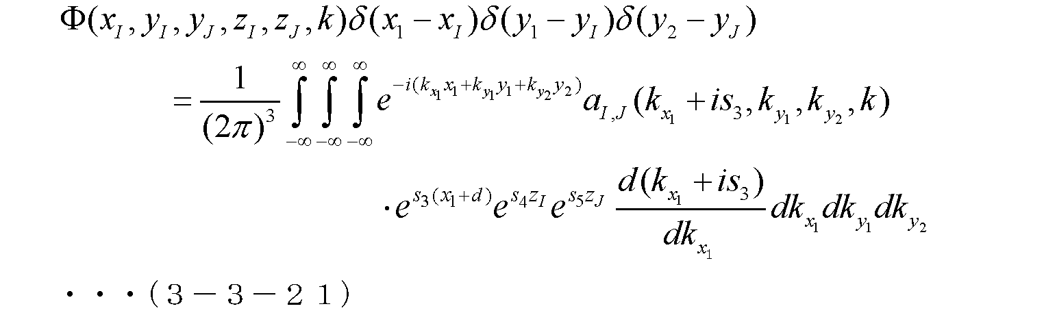
- the above formula (3-3-20) is expressed as the following formula (3-3-21) using the data ⁇ obtained by the measurement on the boundary.
- ⁇ (x I , y I , y J , z I , z J , k) is the transmission point (x I , y I , z I ), reception point (x I +d, y J , z J ) and wavenumber k
- This is the measurement data of The following equation (3-3-22) is obtained by Fourier transforming both sides of equation (3-3-21).
- equation (3-3-23) is obtained as a result of integration with respect to x 1 , y 1 , and y 2 in equation (3-3-22).
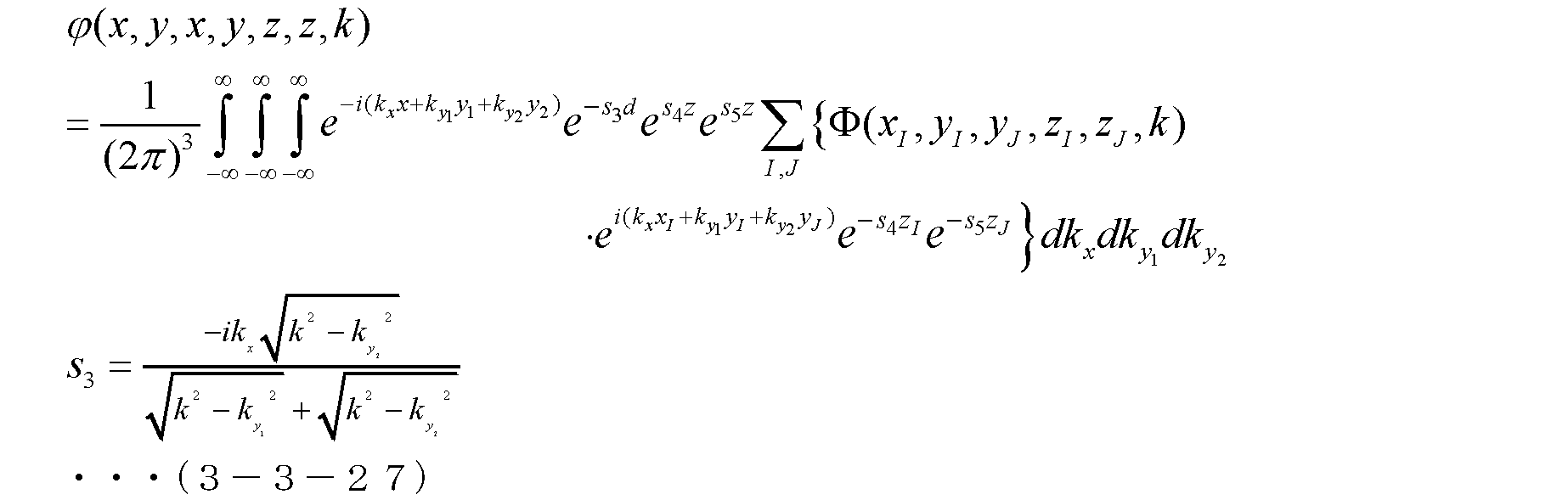
- a scattered field function is obtained from the following formula (3-3-26) from the formulas (3-3-15) and (3-3-25).
- the imaging function ⁇ is obtained by the following equation (3-3-28) by integrating with respect to k.
- the imaging function can be derived using a combination of multiple scattered field functions for multiple combinations of transmit and receive array antennas.
- multiple scattered field functions are combined into one scattered field function, and the imaging function is derived by limit manipulation of the scattered field functions.
- each of the plurality of scattered field functions may be a scattered field function expressed by Equation (3-3-26), and the synthesis may be linear addition.
- a cylindrical surface is shown as the curved surface boundary of the region, but the curved surface boundary of the region may not be a cylindrical surface.
- the above process may be applied not only to the tangent plane to the cylindrical surface, but also to the tangent plane to other curved surface boundaries.
- variable conversion from f to k is easy when there is no dispersion of the dielectric constant.
- the dielectric constant changes depending on the frequency in applications such as living organisms.
- the frequency dependence of the permittivity is taken into account.
- the dielectric constant is about 60% in the 14-20 GHz range compared to the 1-5 GHz range.
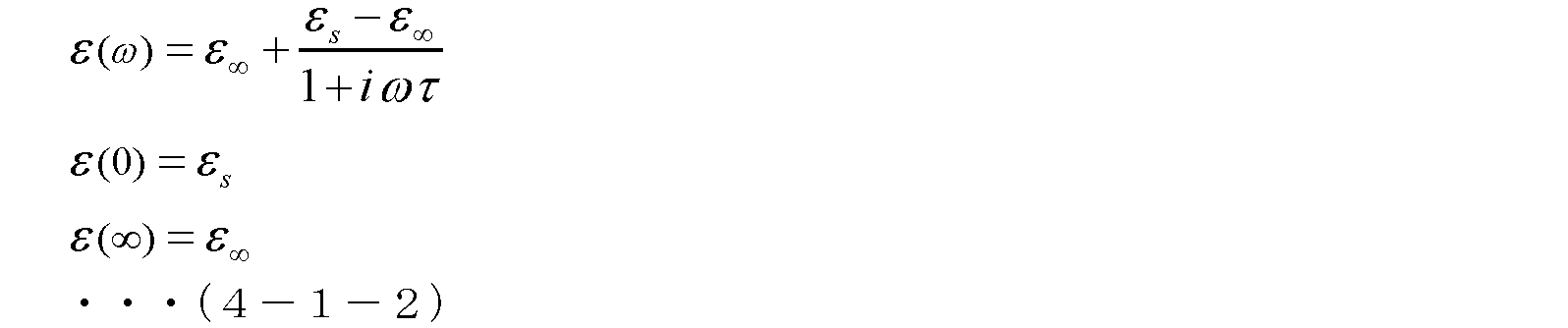
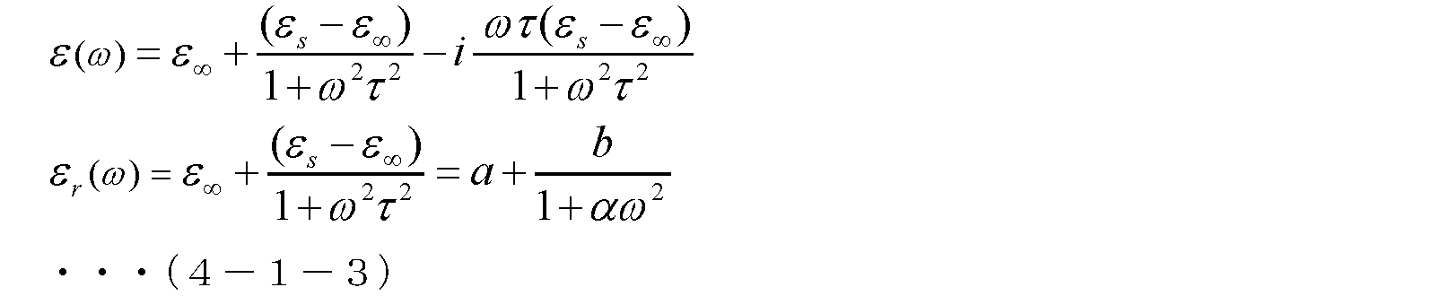
- the equations for the frequency dependence of the Debye permittivity are shown in the following equations (4-1-2) and (4-1-3).
- ⁇ indicates angular frequency.
- ⁇ ( ⁇ ) denotes the complex permittivity at ⁇ .
- i indicates an imaginary unit.
- ⁇ indicates the relaxation time.
- ⁇ r ( ⁇ ) denotes the real part of the complex permittivity at ⁇ .
- a, b and ⁇ represent constants.
- a, b, and ⁇ are parameters that indicate the correspondence between frequency change and permittivity change according to Debye relaxation.
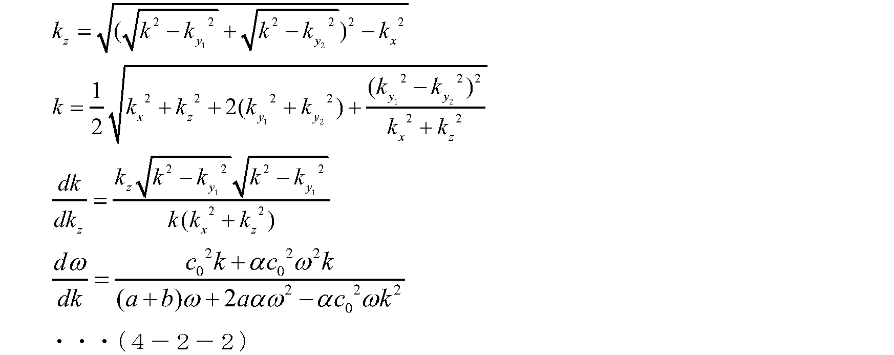
- imaging functions are considered for measuring data by S-Arrays at planar boundaries to produce an image of the interior of a dielectric dispersive medium. Since the time factor is e ⁇ i ⁇ t , integration is performed at frequency ⁇ instead of k in equation (3-2-1) when frequency dependence of permittivity is considered. As a result, imaging functions are obtained as in the following equations (4-2-1) and (4-2-2).
- imaging functions are considered for measuring data by S-Arrays at curved boundaries to generate an image of the interior of a dielectric dispersive medium. Since the time factor is e ⁇ i ⁇ t , integration is performed at frequency ⁇ instead of k in equation (3-3-28) when frequency dependence of permittivity is considered. As a result, imaging functions are obtained as in the following equations (4-3-1) and (4-3-2).
- the waves are, for example, radio waves, and may be microwaves, millimeter waves, terahertz waves, or the like. Also, light, sound, or the like may be used as the wave motion. Objects in the area may be living organisms, manufactured products, natural materials, or the like. In particular, the imaging device may be used for mammography and the object may be a breast.
- the scatterers included in the object within the region correspond to portions having physical properties different from those of the surrounding medium.
- this physical property is a physical property corresponding to wave reflectance. If radio waves are used as waves, the physical property may be dielectric constant. Scatterers included in the object may be reinforcing bars included in reinforced concrete, tumors included in the breast, or the like. Also, the area to be measured may be equivalent to the area of the object.
- FIG. 14 is a basic configuration diagram of a visualization device according to this embodiment.
- the imaging device 100 shown in FIG. 14 comprises a transmitter array 101 , a receiver array 102 and an information processing circuit 103 .
- the imaging device 100 may also include a display 104 .
- the transmitter array 101 is a circuit that transmits waves. Specifically, transmitter array 101 includes a plurality of transmitters 111 arranged in a straight line. Each transmitter 111 then transmits waves.
- the imaging device 100 may comprise multiple transmitter columns 101 parallel to each other.
- the receiver array 102 is a circuit that receives waves. Specifically, the receiver array 102 includes a plurality of receivers 112 arranged on another straight line parallel to the straight line on which the plurality of transmitters 111 are arranged. Each receiver 112 then receives the waves. Also, the receiver array 102 is spaced apart from the transmitter array 101 . That is, receiver array 102 is remote from transmitter array 101 .
- the imaging device 100 may comprise multiple receiver rows 102 parallel to each other.
- the information processing circuit 103 is a circuit that performs information processing. Specifically, the information processing circuit 103 visualizes the structure of the scatterers included in the object within the area based on the measurement data obtained by the transmitter array 101 and the receiver array 102 . For example, when the information processing circuit 103 visualizes the structure of the scatterer based on the measurement data, the information processing circuit 103 performs arithmetic processing shown in the theory described above.
- the information processing circuit 103 may be a computer or a processor of a computer.
- the information processing circuit 103 may perform information processing by reading a program from memory and executing the program. Further, the information processing circuit 103 may be a dedicated circuit that visualizes the structure of the scatterers based on the measurement data.
- the information processing circuit 103 may generate an image showing the structure of the scatterer in order to visualize the structure of the scatterer.
- the information processing circuit 103 may visualize the structure of the scatterer by outputting an image showing the structure of the scatterer to the display 104 or the like. Alternatively, the information processing circuit 103 may visualize the structure of the scatterer by outputting an image showing the structure of the scatterer to a printer (not shown). Alternatively, the information processing circuit 103 may visualize the structure of the scatterer by transmitting the image as electronic data to another device (not shown) through wired or wireless communication.
- the display 104 is a display device such as a liquid crystal display. Note that the display 104 is an optional component and not an essential component. Also, the display 104 may be an external device that does not constitute the imaging device 100 .
- FIG. 15 is a flow chart showing the basic operation of the imaging device 100 shown in FIG. Specifically, the transmitter array 101, the receiver array 102, the information processing circuit 103, etc. of the imaging apparatus 100 shown in FIG. 14 perform the operations shown in FIG.
- the plurality of transmitters 111 of the transmitter array 101 transmit waves to the area to be measured (S101). For example, multiple transmitters 111 transmit waves in sequence. Also, the plurality of receivers 112 of the receiver array 102 receive waves from the area (S102). For example, multiple receivers 112 receive waves in parallel. Received waves may also be described as scattered waves. Then, the information processing circuit 103 visualizes the structure of the scatterers included in the object within the area using the measurement data obtained by the plurality of transmitter arrays 101 and the plurality of receiver arrays 102 (S103).
- the information processing circuit 103 When visualizing the structure of the scatterer, the information processing circuit 103 first derives a visualization function corresponding to the scattered field function related to wave scattering according to the measurement data and the distance.
- the measurement data is measurement data obtained by a combination of all or part of the plurality of transmitters 111 and the plurality of receivers 112 .
- the distance is the distance between the straight line on which the plurality of transmitters 111 are arranged and the straight line on which the plurality of receivers 112 are arranged. Then, the information processing circuit 103 visualizes the structure of the scatterers included in the object within the region using the visualization function.
- the imaging device 100 can acquire sufficient information as measurement data according to various combinations of the plurality of transmitters 111 of the transmitter array 101 and the plurality of receivers 112 of the receiver array 102. .
- the imaging device 100 is provided with a space between the transmitter row 101 and the receiver row 102, it is possible to appropriately transmit the waves to the area and receive the waves from the area appropriately. can be done.
- the imaging device 100 appropriately visualizes the structure of the scatterer using the wave measurement data and the imaging function derived according to the distance between the transmitter array 101 and the receiver array 102. can be done.
- the imaging apparatus 100 simplifies arithmetic processing compared to the case where the transmitter 111 and the receiver 112 are arbitrarily placed. be able to. Therefore, the imaging device 100 can suppress complication of arithmetic processing. That is, the imaging apparatus 100 can visualize the structure of the scatterer contained in the object in the region using the wave motion, and while suppressing the complexity of the arithmetic processing, the spatial resolution in the visualization of the structure of the scatterer can be improved. can increase
- the information processing circuit 103 may derive the scattered field function according to the measurement data and the distance. The information processing circuit 103 may then derive an imaging function according to the scattered field function.
- (x 1 , y 1 , z) indicates the wave transmission position.
- (x 2 , y 2 , z) indicates the wave receiving position.
- k indicates the wave number of the wave.
- D indicates a region.
- ( ⁇ , ⁇ , ⁇ ) correspond to the reflection position of the wave.
- ⁇ corresponds to the unknown reflectance at the reflection position.
- the imaging apparatus 100 can derive a scattered field function determined on the assumption that the transmission position and the reception position have the same z-coordinate, and can derive the imaging function according to the scattered field function. can. Accordingly, the imaging device 100 appropriately performs the A scattered field function and an imaging function can be derived.
- the information processing circuit 103 may derive the scattered field function by solving an equation satisfied by the scattered field function.
- c indicates the wave propagation speed.
- t indicates the time from wave transmission to reception.
- the imaging device 100 can analytically derive the solution of the equation satisfied by the scattered field function as the scattered field function. Therefore, the imaging device 100 can efficiently derive an appropriate scattered field function.
- the visualization function is may be expressed as Here, (x, y, z) indicate the imaging target position.
- the imaging device 100 can derive the imaging function according to the limit manipulation of the scattered field function. Accordingly, the imaging apparatus 100 can visualize the state of scattering within the region, and can appropriately visualize the structure of the scatterers included in the object within the region.
- the information processing circuit 103 may be derived as a scattered field function.
- k x1 , k y1 and k y2 denote wavenumbers related to x 1 , y 1 and y 2 of the scattered field function. d indicates the distance.
- the imaging device 100 can appropriately reflect the wave measurement data and the distance between the transmitter array 101 and the receiver array 102 in the scattered field function. Therefore, the imaging device 100 can derive a scattered field function that appropriately represents the state of scattering.
- the information processing circuit 103 may be derived as a visualization function.
- (x, y, z) indicates the imaging target position.
- k x1 , k y1 and k y2 denote wavenumbers for x 1 , y 1 and y 2 of the scattered field function.
- d indicates the distance.
- the imaging device 100 can appropriately reflect the wave measurement data and the distance between the transmitter array 101 and the receiver array 102 in the imaging function.
- the imaging device 100 can derive an imaging function that adequately represents the scattering state.
- the imaging device 100 may include a plurality of transmitter arrays 101 as the transmitter array 101, a plurality of receiver arrays 102 as the receiver array 102, or a plurality of transmitter arrays 101 and 102 as the transmitter array 101 and the receiver array 102.
- a column 101 and a plurality of receiver columns 102 may be provided.
- the imaging device 100 can acquire sufficient information as measurement data in accordance with multiple combinations of the transmitter array 101 and the receiver array 102 .
- the imaging apparatus 100 can establish a multi-static relationship with respect to the transmitter row 101 and the receiver row 102 in two directions, parallel and orthogonal. Therefore, the imaging device 100 can appropriately visualize the structure of the scatterers included in the object within the area.
- the information processing circuit 103 may perform may be derived as a visualization function.
- (x, y, z) indicates the imaging target position.
- k x1 , k y1 and k y2 denote wavenumbers for x 1 , y 1 and y 2 of the scattered field function.
- dj indicates the distance.
- the imaging device 100 can appropriately reflect the wave measurement data and the distance between the transmitter array 101 and the receiver array 102 in the imaging function. Specifically, the imaging device 100 corresponds to the distance between the transmitter array 101 and the receiver array 102 for the measurement data obtained according to a plurality of combinations of the transmitter array 101 and the receiver array 102. By performing linear summation, it is possible to derive an imaging function that adequately represents the state of scattering.
- the information processing circuit 103 may be derived as a visualization function.
- (x, y, z) indicates the imaging target position.
- k x1 , k y1 and k y2 denote wavenumbers for x 1 , y 1 and y 2 of the scattered field function.
- d indicates the distance.
- ⁇ indicates the angular frequency of the wave.
- c 0 denotes the wave propagation velocity in vacuum.
- a, b and ⁇ denote parameters related to Debye relaxation.
- the visualization device 100 can derive a visualization function that reflects parameters relating to Debye relaxation. Therefore, the imaging device 100 can suppress accuracy degradation that occurs depending on the wave frequency.
- the information processing circuit 103 may derive a scattered field function according to the measurement data and the distance. The information processing circuit 103 may then derive an imaging function according to the scattered field function.
- (x 1 , y 1 , z 1 ) indicates the wave transmission position.
- (x 2 , y 2 , z 2 ) indicates the wave receiving position.
- k indicates the wave number of the wave.
- D indicates the area, and ( ⁇ , ⁇ , ⁇ ) correspond to the reflection position of the wave.
- ⁇ corresponds to the unknown reflectance at the reflection position.
- the imaging device 100 can derive a scattered field function determined on the assumption that the transmission position and the reception position can have different z-coordinates, and derive the imaging function according to the scattered field function. can be done. Therefore, the imaging device 100 measures data obtained using the plurality of transmitters 111 of the transmitter array 101 and the plurality of receivers 112 of the receiver array 102 along the tangential plane of the region having the curved boundary. can properly derive the scattered field function and the imaging function according to
- the information processing circuit 103 may derive the scattered field function by solving an equation satisfied by the scattered field function.
- the imaging device 100 can analytically derive the solution of the equation satisfied by the scattered field function as the scattered field function. Therefore, the imaging device 100 can efficiently derive an appropriate scattered field function.
- the visualization function is may be expressed as Here, (x, y, z) indicate the imaging target position.
- the imaging device 100 can derive the imaging function using the scattered field function to which the imaging target position is input. Accordingly, the imaging apparatus 100 can visualize the state of scattering within the region, and can appropriately visualize the structure of the scatterers included in the object within the region.
- the information processing circuit 103 may be derived as a scattered field function.
- k x1 , k y1 and k y2 denote wavenumbers related to x 1 , y 1 and y 2 of the scattered field function.
- d indicates the distance.
- ⁇ (x I , y I , y J , z I , z J , k) is a transmission position (x I , y I , z I ) and a reception position (x I +d, y J , z J ) Measured data in one case is shown.
- the imaging device 100 can appropriately reflect the wave measurement data and the distance between the transmitter array 101 and the receiver array 102 in the scattered field function. Therefore, the imaging device 100 can derive a scattered field function that appropriately represents the state of scattering.
- the information processing circuit 103 may be derived as a visualization function.
- (x, y, z) indicates the imaging target position.
- k x1 , k y1 and k y2 denote wavenumbers for x 1 , y 1 and y 2 of the scattered field function.
- d indicates the distance.
- ⁇ ( xI , yI , yJ , zI, zJ , k) has a transmission position of ( xI , yI , zI ) and a reception position of ( xI + d , yJ , zJ ) shows the measurement data in the case of
- the imaging device 100 can appropriately reflect the wave measurement data and the distance between the transmitter array 101 and the receiver array 102 in the imaging function.
- the imaging device 100 can derive an imaging function that adequately represents the scattering state.
- the information processing circuit 103 may derive an imaging function using a synthesis of a plurality of scattered field functions for a plurality of combinations of the transmitter array 101 and the receiver array 102 .
- k x1 , k y1 and k y2 denote wavenumbers related to x 1 , y 1 and y 2 of the scattered field function.
- d indicates the distance.
- ⁇ ( xI , yI , yJ , zI, zJ , k) has a transmission position of ( xI , yI , zI ) and a reception position of ( xI + d , yJ , zJ ) shows the measurement data in the case of
- the imaging device 100 appropriately expresses the state of scattering by combining wave measurement data and a plurality of scattered field functions that reflect the distance between the transmitter array 101 and the receiver array 102.
- a visualization function can be derived.
- the information processing circuit 103 may be derived as a visualization function.
- (x, y, z) indicates the imaging target position.
- k x1 , k y1 and k y2 denote wavenumbers for x 1 , y 1 and y 2 of the scattered field function.
- d indicates the distance.
- ⁇ indicates the angular frequency of the wave.
- c 0 denotes the wave propagation velocity in vacuum.
- a, b and ⁇ denote parameters related to Debye relaxation.
- the visualization device 100 can derive a visualization function that reflects parameters relating to Debye relaxation. Therefore, the imaging device 100 can suppress accuracy degradation that occurs depending on the wave frequency.
- the scattered field function may be defined as a function in which a wave transmission position and a wave reception position are input and a value indicating the wave at the reception position is output.
- the imaging function may be determined based on values output from the scattered field function by inputting imaging target positions as the transmission position and the reception position into the scattered field function.
- the information processing circuit 103 may derive a scattered field function using the measurement data as a boundary condition, and derive an imaging function using the scattered field function.
- the scattered field function and imaging function may reflect the distance between the straight line on which the plurality of transmitters 111 are arranged and the straight line on which the plurality of receivers 112 are arranged.
- the transmitter array 101, the receiver array 102, the information processing circuit 103, the scattered field function, the imaging function, and the like shown in the basic configuration and basic operation described above may include other functions shown in the present embodiment. components, formulas and variables, etc. may be applied as appropriate.
- the scattered field function, the imaging function, and the like shown in the present embodiment may be modified as appropriate and applied.
- a mathematical expression that expresses substantially the same content as the above-described mathematical expression in another expression may be used, or another mathematical expression derived based on the above-described theory may be used.
- FIG. 16 is a block diagram showing a specific configuration of imaging device 100 shown in FIG.
- the transmitter array 101 and receiver array 102 of the imaging device 100 shown in FIG. 14 may be included in the multi-static array antenna 1008.
- the information processing circuit 103 of the imaging device 100 shown in FIG. 14 may correspond to one or more of the multiple components shown in FIG. Specifically, for example, the information processing circuit 103 may correspond to the signal processing computer 1005 . Also, the display 104 shown in FIG. 14 may correspond to the signal monitoring device 1006 .
- the microwave signal used in the imaging device 100 is a pseudo-random time-series signal (PN code: Pseudo Noise Code) having frequency components of DC to 20 GHz.
- PN code Pseudo Noise Code
- This signal is output from the FPGA board 1002 for PN code generation. More specifically, there are two types of this signal.
- One type of signal (LO signal: local oscillator signal) is sent through the delay circuit (digital control board 1003) to the RF detector circuit (RF detector board 1007).
- the other type of signal (RF signal: Radio Frequency Signal) is sent to the transmitting microwave UWB antenna of the multi-static array antenna 1008 and radiated.
- a scattered microwave signal is received by the receiving UWB antenna of the multi-static array antenna 1008 and sent to the RF detection circuit (RF detection board 1007).
- the transmission/reception signals pass through the antenna element selection switch (UWB antenna RF switch 1004).
- the delayed signal (LO signal) is delayed by 1/ 2n times (n is an integer greater than 2) the time at which the value of the PN code changes.
- the detected signal is A/D converted by the signal processing computer 1005 and stored as an IF signal (Intermediate Frequency Signal). Information indicating the detected signal may also be displayed on the signal monitoring device 1006 .
- the timing of these series of operations is controlled by the microprocessor in the digital control board 1003 so as to synchronize with the signal (distance signal or free run signal) from the rangefinder 1001.
- the microprocessor in the digital control board 1003 sends Switch switching signals, PN code sweep triggers, and the like.
- the signal processing computer 1005 also uses the A/D-converted and stored signals to perform three-dimensional reconstruction and display a three-dimensional image.
- the signal processing calculator 1005 may also perform signal calibration.
- the signal processing computer 1005 may display raw waveforms.
- the signal processing computer 1005 may store a three-dimensional image or the like in the memory 1009 .
- the configuration shown in FIG. 16 is an example, and the configuration of imaging device 100 is not limited to the configuration shown in FIG. A part of the configuration shown in FIG. 16 may be omitted or changed.
- the imaging method including the steps performed by each component of the imaging device may be executed by any device or system.
- part or all of the imaging method may be performed by a computer including a processor, memory, input/output circuitry, and the like.
- the imaging method may be executed by the computer executing a program for causing the computer to execute the imaging method.
- the above program may be recorded on a non-temporary computer-readable recording medium.
- each component of the imaging apparatus may be configured with dedicated hardware, may be configured with general-purpose hardware that executes the above programs, etc., or may be configured with a combination of these. good.
- the general-purpose hardware may be composed of a memory in which a program is recorded, a general-purpose processor that reads and executes the program from the memory, and the like.
- the memory may be a semiconductor memory, a hard disk, or the like, and the general-purpose processor may be a CPU or the like.
- dedicated hardware may be configured with a memory, a dedicated processor, and the like.
- a dedicated processor may refer to a memory for recording measurement data and perform the imaging method described above.
- each component of the imaging device may be an electric circuit.
- These electric circuits may form one electric circuit as a whole, or may be separate electric circuits. Further, these electric circuits may correspond to dedicated hardware, or may correspond to general-purpose hardware for executing the above-described programs and the like.
- One aspect of the present disclosure is useful for an imaging device that visualizes the structure of scatterers contained in an object within an area using waves, and is applicable to geophysical exploration, medical diagnosis, and the like.
- REFERENCE SIGNS LIST 100 imaging device 101 transmitter array 102 receiver array 103 information processing circuit 104 display 111 transmitter 112 receiver 1001 rangefinder 1002 PN code generation FPGA board 1003 digital control board 1004 UWB antenna RF switch 1005 signal processing computer 1006 signal monitor Apparatus 1007 RF detection board 1008 Multistatic array antenna 1009 Memory
Landscapes
- Physics & Mathematics (AREA)
- Health & Medical Sciences (AREA)
- Engineering & Computer Science (AREA)
- General Physics & Mathematics (AREA)
- Life Sciences & Earth Sciences (AREA)
- Remote Sensing (AREA)
- Pathology (AREA)
- General Health & Medical Sciences (AREA)
- Electromagnetism (AREA)
- Radar, Positioning & Navigation (AREA)
- Biochemistry (AREA)
- Analytical Chemistry (AREA)
- Chemical & Material Sciences (AREA)
- Immunology (AREA)
- Molecular Biology (AREA)
- Biomedical Technology (AREA)
- Veterinary Medicine (AREA)
- Animal Behavior & Ethology (AREA)
- Surgery (AREA)
- Medical Informatics (AREA)
- Heart & Thoracic Surgery (AREA)
- Data Mining & Analysis (AREA)
- Biophysics (AREA)
- Theoretical Computer Science (AREA)
- Spectroscopy & Molecular Physics (AREA)
- Radiology & Medical Imaging (AREA)
- Nuclear Medicine, Radiotherapy & Molecular Imaging (AREA)
- Public Health (AREA)
- Mathematical Physics (AREA)
- Computer Networks & Wireless Communication (AREA)
- Computational Mathematics (AREA)
- General Engineering & Computer Science (AREA)
- Mathematical Optimization (AREA)
- Algebra (AREA)
- Pure & Applied Mathematics (AREA)
- Databases & Information Systems (AREA)
- Software Systems (AREA)
- Mathematical Analysis (AREA)
- Toxicology (AREA)
- Radar Systems Or Details Thereof (AREA)
Abstract
Description























本実施の形態における映像化装置は、波動を用いて、領域内の物体に含まれる散乱体の構造を可視化する。以下、本実施の形態における映像化装置をその基礎となる技術及び理論なども含めて、詳細に説明する。
本開示ではS-Array(super-array)散乱場理論によるマイクロ波イメージング技術について述べる。
<II-1 平面境界の1次元配列MS逆散乱理論>
1次元のアレイアンテナを用いた映像化装置において対象物の映像化に用いられている方法は、極めて簡単であり、単に次式(2-1-1)の波動方程式を解くだけである。



















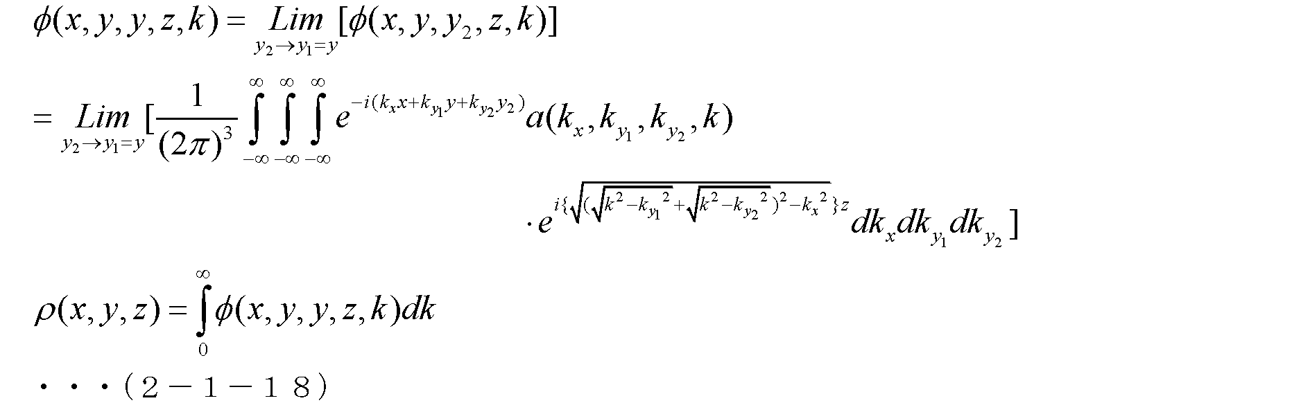
領域の境界面が曲面の場合の逆散乱理論について述べる。






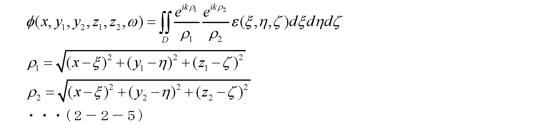












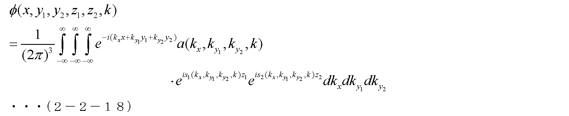
図8は、前方散乱における送信点及び受信点の関係を示す概念図である。前方散乱が後方散乱(II-2)と異なる点は、送信点r1のz座標と受信点r2のz座標と間に全ての散乱点のz座標が入っている点である。r1とr2とがそれぞれ∂D1上と∂D2上とで同じx座標に位置するという拘束のもとに自由に移動し、散乱データが計測される。このシステムにおける散乱場関数は次式(2-3-1)のように定義される。






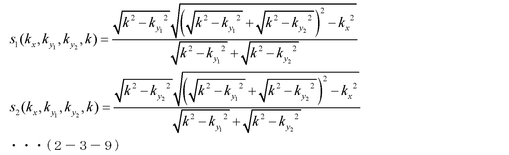



まず、既存の2次元配列の場合の理論を説明する。
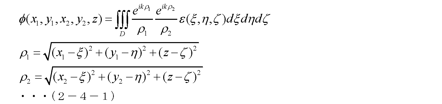


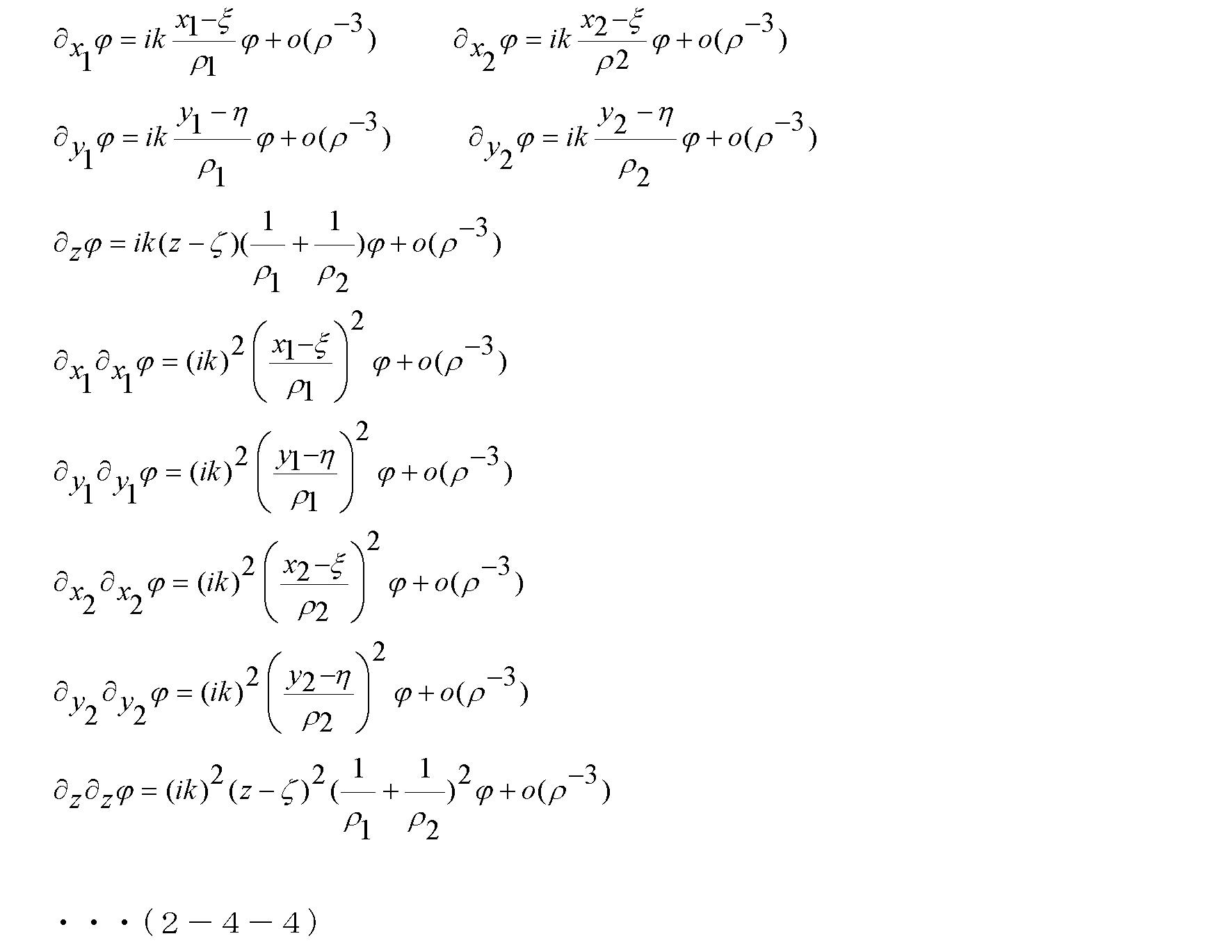






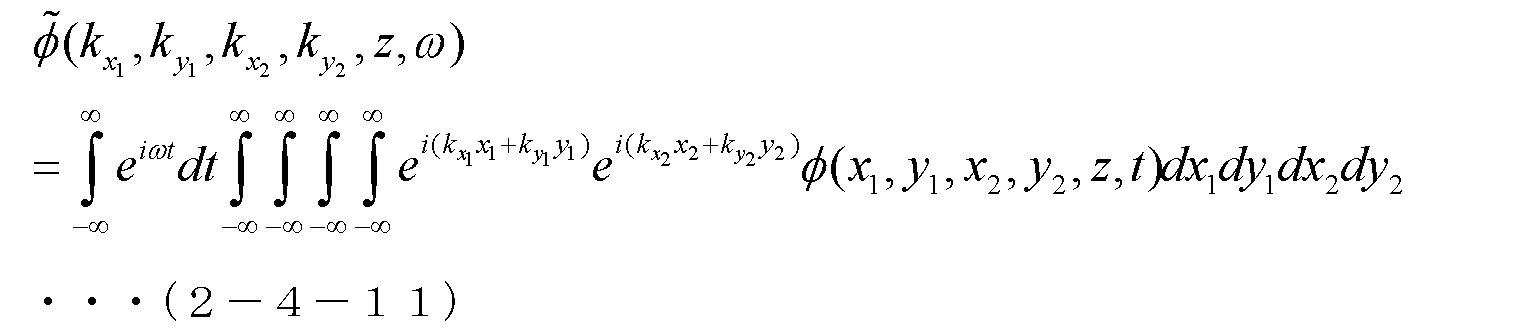

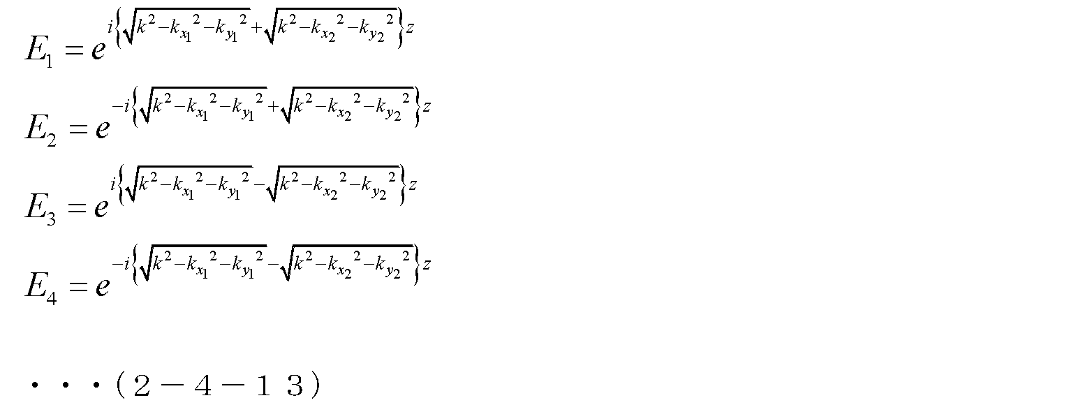



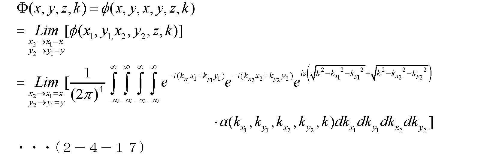


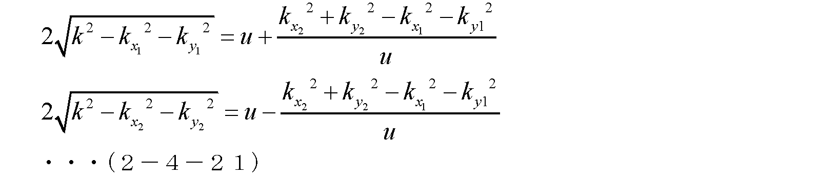



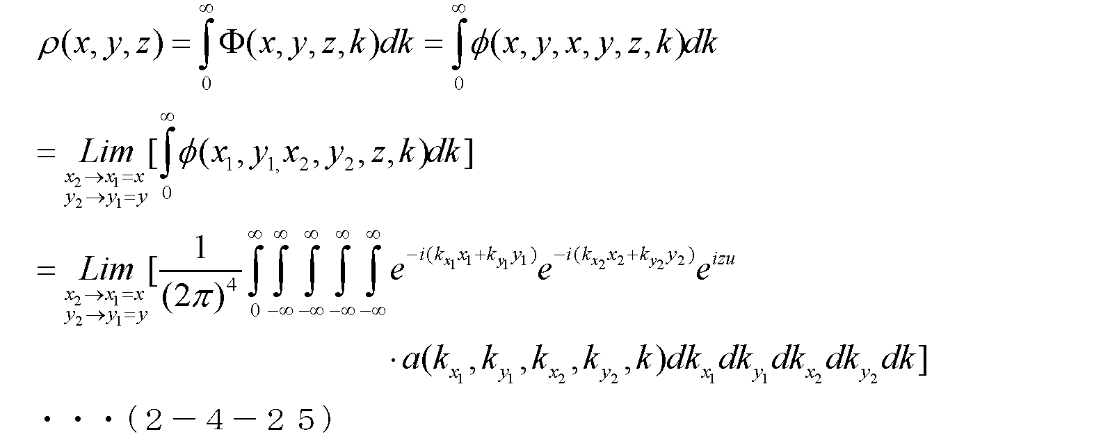
図10は、曲面における送信点及び受信点の関係を示す概念図である。曲面の境界条件を用いるため、送信点と受信点のz座標が異なると仮定される。したがって、散乱場関数は、次式(2-5-1)のように表現される。














<III-1 平面境界及び準2次元配列のS-Array散乱場理論>
ここでは、図3に示された構成が用いられる。また、2次元配列に関する式(2-4-10)が検討の出発点として用いられる。以下の式(3-1-1)は、式(2-4-10)と同じ式である。









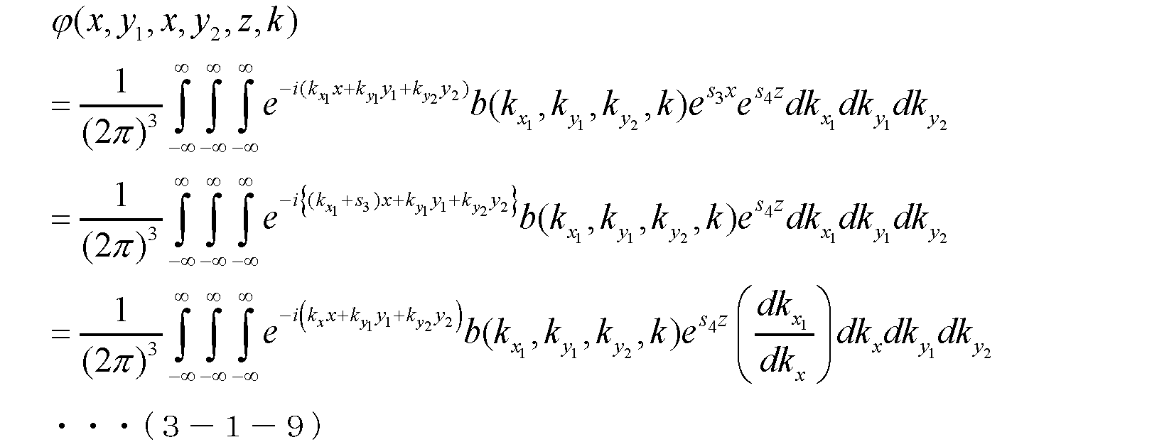


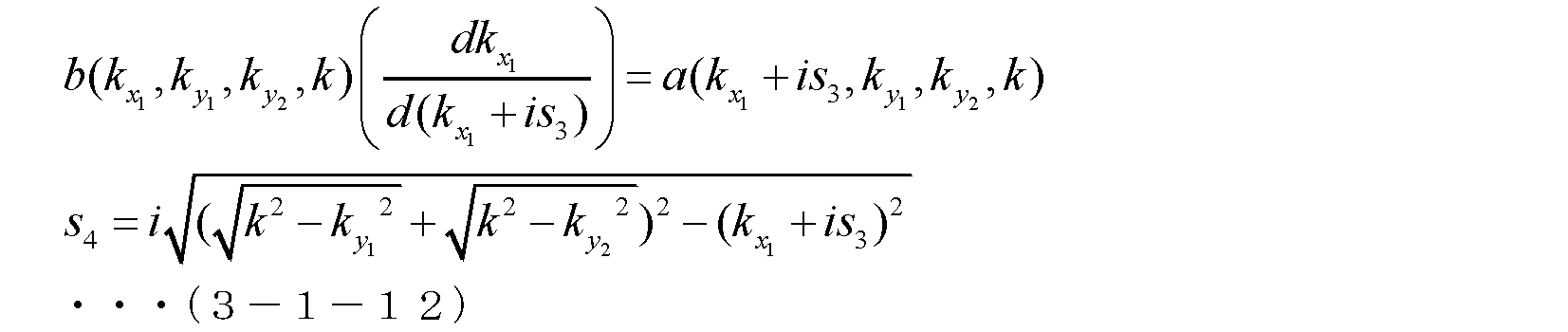

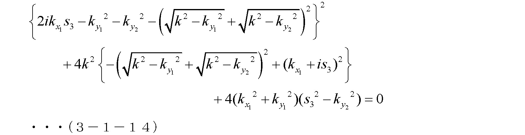


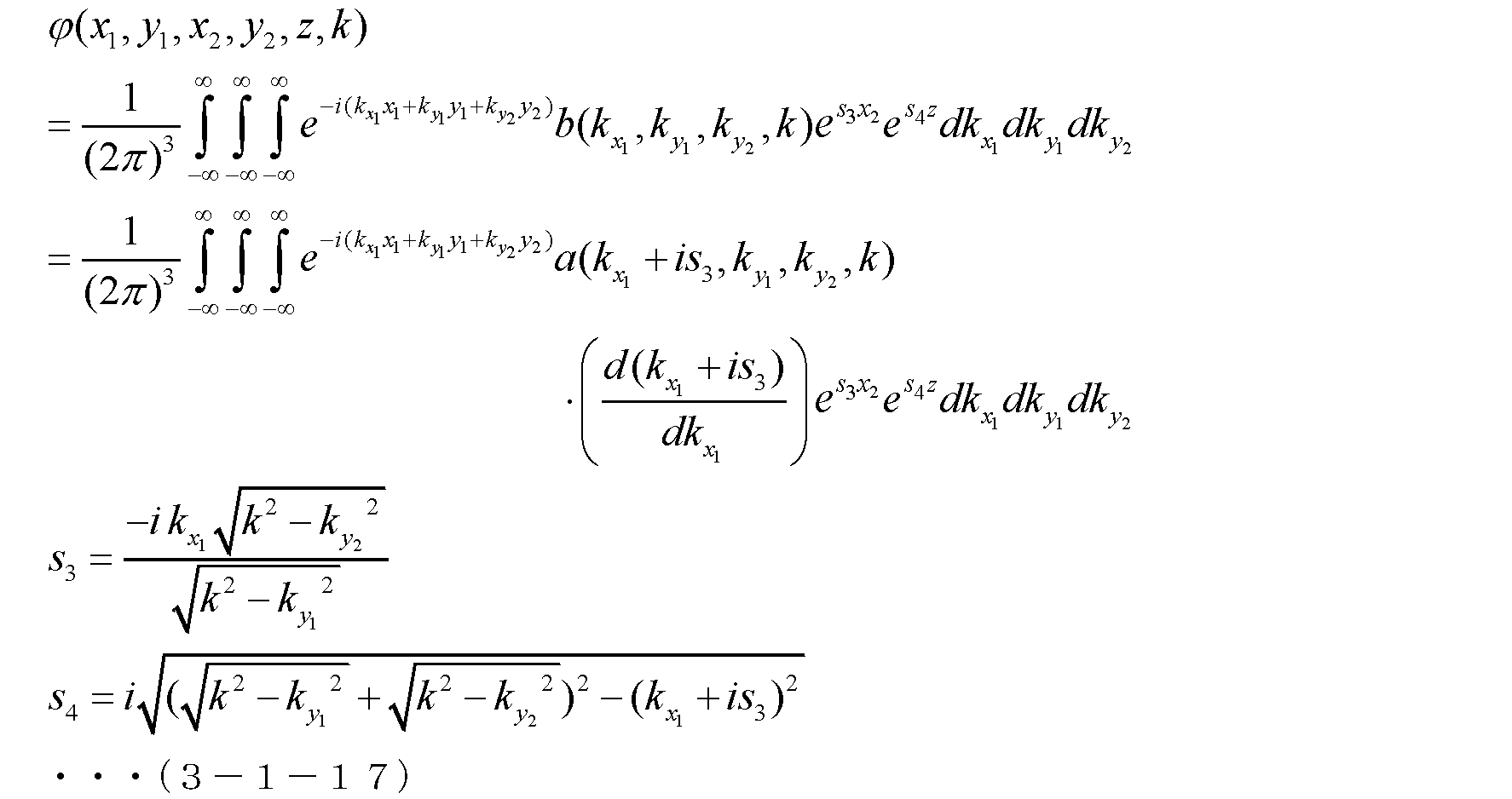
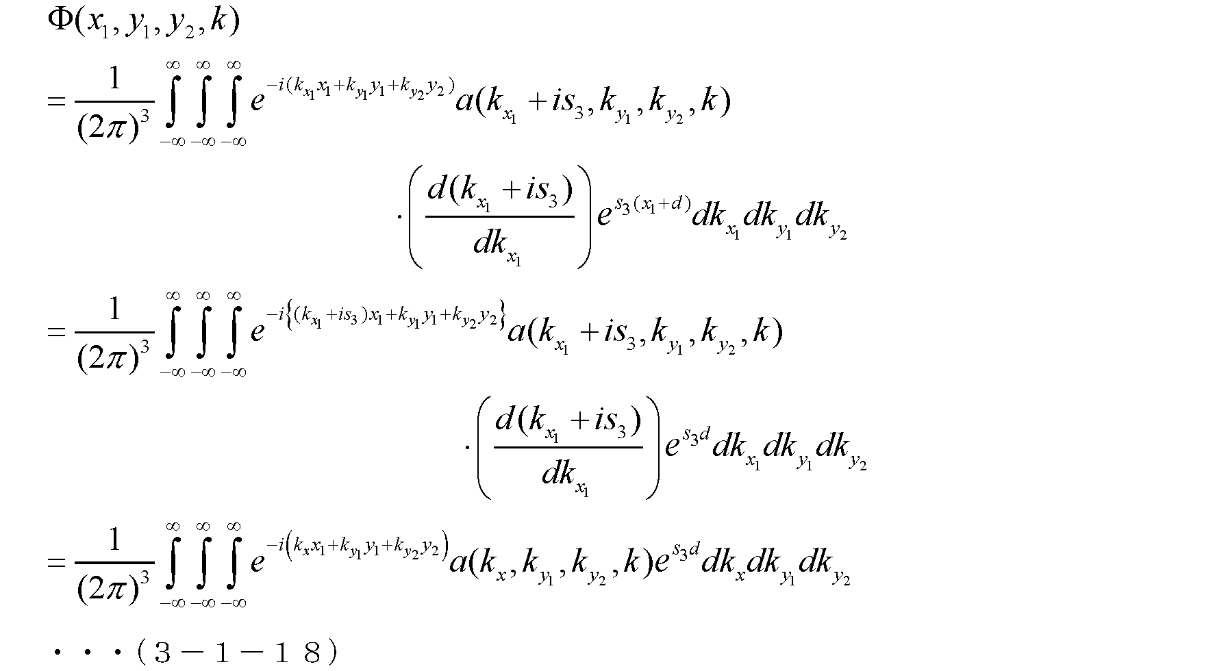



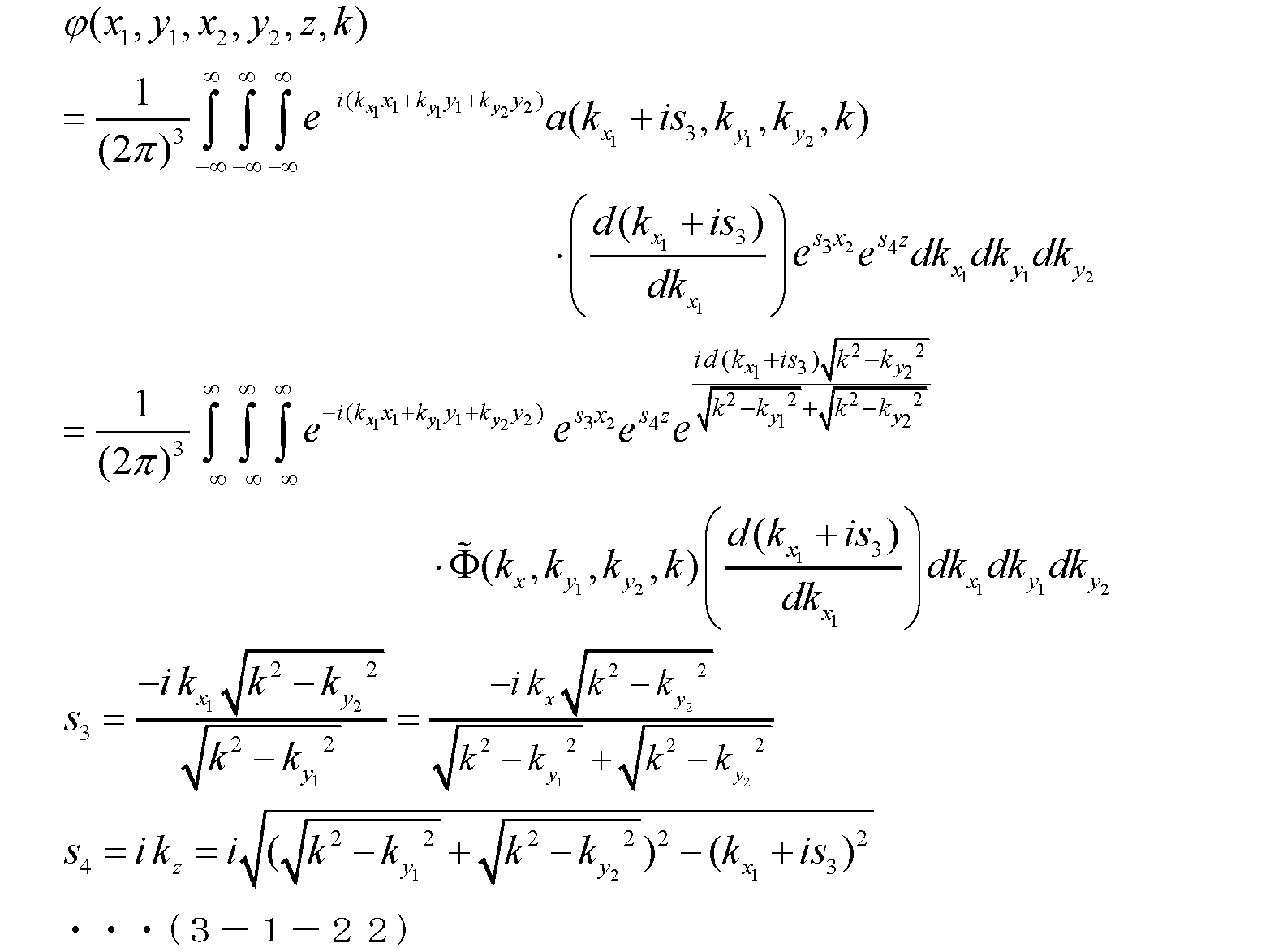
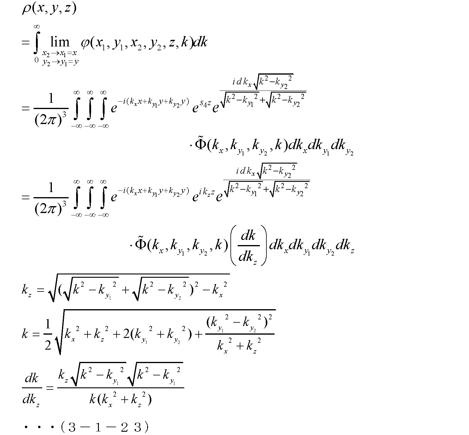
図11は、複数列リニアアレイアンテナを示す図である。図11に示された複数列リニアアレイアンテナは、1列の送信アレイアンテナTAと、n列の受信アレイアンテナRA1、RA2、RA3、・・・、RAnとを含む。各アンテナ素子の偏波方向は、x方向のほかにy方向の場合もありうる。またTAとRAとが入れ替わってもよい。このような配列の場合へIII-1節の準2次元配列MS逆散乱を応用する。
以下では、領域の境界すなわち散乱データを計測する境界面が、曲率の大きくない曲面である場合のS-Array散乱場理論を説明する。






















<IV-1 基礎理論>
III章で求められた再構成の式を用いるにあたり誘電率の分散性の有無が考慮されてもよい。誘電率の分散性がない場合、周波数fと波数kとは次式(4-1-1)のような簡単な関係を有する。ここで、εrは比誘電率であり、c0は真空中の電磁波の速度である。





ここでは、平面境界においてS-Arrayによってデータを計測して、誘電分散性媒質の内部の映像を生成するための映像化関数が検討される。時間の因子がe-iωtであるため、誘電率に周波数依存性があることが考慮される場合、式(3-2-1)においてkの代わりに周波数ωで積分が行われる。これにより、以下の式(4-2-1)及び式(4-2-2)のように映像化関数が得られる。

ここでは、曲面境界においてS-Arrayによってデータを計測して、誘電分散性媒質の内部の映像を生成するための映像化関数が検討される。時間の因子がe-iωtであるため、誘電率に周波数依存性があることが考慮される場合、式(3-3-28)においてkの代わりに周波数ωで積分が行われる。これにより、以下の式(4-3-1)及び式(4-3-2)のように映像化関数が得られる。

上述された内容に基づいて、以下に、波動を用いて領域内の物体に含まれる散乱体の構造を可視化する映像化装置の構成及び動作を示す。
























以上、映像化装置の態様を実施の形態に基づいて説明したが、映像化装置の態様は、実施の形態に限定されない。実施の形態に対して当業者が思いつく変形が施されてもよいし、実施の形態における複数の構成要素が任意に組み合わされてもよい。例えば、実施の形態において特定の構成要素によって実行される処理を特定の構成要素の代わりに別の構成要素が実行してもよい。また、複数の処理の順序が変更されてもよいし、複数の処理が並行して実行されてもよい。
101 送信器列
102 受信器列
103 情報処理回路
104 ディスプレイ
111 送信器
112 受信器
1001 距離計
1002 PN符号生成用FPGAボード
1003 デジタル制御ボード
1004 UWBアンテナRFスイッチ
1005 信号処理計算機
1006 信号モニタ装置
1007 RF検波ボード
1008 マルチスタティックアレイアンテナ
1009 メモリ
Claims (21)
- 直線上に配列され、計測対象の領域へ波動を送信する複数の送信器を含む送信器列と、
前記複数の送信器が配列される直線に平行な別の直線上に配列され、前記領域から前記波動を受信する複数の受信器を含み、前記送信器列から間隔が設けられた受信器列と、
前記複数の送信器と前記複数の受信器との全部又は一部の組み合わせによって得られる計測データ、及び、前記複数の送信器が配列される直線と前記複数の受信器が配列される直線との間の距離に従って、前記波動の散乱に関する散乱場関数に対応する映像化関数を導出し、前記映像化関数を用いて、前記領域内の物体に含まれる散乱体の構造を可視化する情報処理回路とを備える
映像化装置。 - 前記情報処理回路は、前記計測データ及び前記距離に従って前記散乱場関数を導出し、前記散乱場関数に従って前記映像化関数を導出し、
前記散乱場関数は、

ρ1及びρ2は、

(x1、y1、z)は、前記波動の送信位置を示し、(x2、y2、z)は、前記波動の受信位置を示し、kは、前記波動の波数を示し、Dは、前記領域を示し、(ξ、η、ζ)は、前記波動の反射位置に対応し、εは、前記反射位置における未知の反射率に対応する
請求項1に記載の映像化装置。 - 前記情報処理回路は、前記散乱場関数が満たす方程式を解くことにより、前記散乱場関数を導出し、
前記方程式は、

Δ5は、

cは、前記波動の伝搬速度を示し、tは、前記波動の送信から受信までの時間を示す
請求項2に記載の映像化装置。 - 前記映像化関数は、

(x、y、z)は、映像化対象位置を示す
請求項2又は3に記載の映像化装置。 - 前記情報処理回路は、
kx、s3及びs4は、
kx1、ky1及びky2は、前記散乱場関数のx1、y1及びy2に関する波数を示し、dは、前記距離を示し、

請求項2又は3に記載の映像化装置。 - 前記情報処理回路は、
kx、kz、k、dk/dkz及びs4は、


(x、y、z)は、映像化対象位置を示し、kx1、ky1及びky2は、前記散乱場関数のx1、y1及びy2に関する波数を示し、dは、前記距離を示し、

請求項2又は3に記載の映像化装置。 - 前記映像化装置は、前記送信器列として複数の送信器列、前記受信器列として複数の受信器列、又は、前記送信器列及び前記受信器列として複数の送信器列及び複数の受信器列を備える
請求項1に記載の映像化装置。 - 前記映像化装置は、前記送信器列として複数の送信器列、前記受信器列として複数の受信器列、又は、前記送信器列及び前記受信器列として複数の送信器列及び複数の受信器列を備える
請求項2又は3に記載の映像化装置。 - 前記情報処理回路は、

kx、s3及びs4は、
kx1、ky1及びky2は、前記散乱場関数のx1、y1及びy2に関する波数を示し、dは、前記距離を示し、

請求項8に記載の映像化装置。 - 前記情報処理回路は、前記映像化装置が前記送信器列及び前記受信器列として備える1列の送信器列及びn列の受信器列に対して、

kx、kz、k、dk/dkz及びs4は、

(x、y、z)は、映像化対象位置を示し、kx1、ky1及びky2は、前記散乱場関数のx1、y1及びy2に関する波数を示し、djは、前記距離を示し、

請求項8に記載の映像化装置。 - 前記情報処理回路は、前記領域において前記反射率に対応する誘電率が周波数依存性を有する場合、

kx、kz、k、dk/dkz、dω/dk及びs4は、

s3は、

(x、y、z)は、映像化対象位置を示し、kx1、ky1及びky2は、前記散乱場関数のx1、y1及びy2に関する波数を示し、dは、前記距離を示し、ωは、前記波動の角周波数を示し、c0は、真空中の前記波動の伝搬速度を示し、a、b及びαは、デバイ緩和に関するパラメータを示し、

請求項2又は3に記載の映像化装置。 - 前記情報処理回路は、前記計測データ及び前記距離に従って前記散乱場関数を導出し、前記散乱場関数に従って前記映像化関数を導出し、
前記散乱場関数は、

ρ1及びρ2は、

(x1、y1、z1)は、前記波動の送信位置を示し、(x2、y2、z2)は、前記波動の受信位置を示し、kは、前記波動の波数を示し、Dは、前記領域を示し、(ξ、η、ζ)は、前記波動の反射位置に対応し、εは、前記反射位置における未知の反射率に対応する
請求項1に記載の映像化装置。 - 前記情報処理回路は、前記散乱場関数が満たす方程式を解くことにより、前記散乱場関数を導出し、
前記方程式は、

Δ6は、

請求項12に記載の映像化装置。 - 前記映像化関数は、

(x、y、z)は、映像化対象位置を示す
請求項12又は13に記載の映像化装置。 - 前記情報処理回路は、
kx、s3、s4及びs5は、

kx1、ky1及びky2は、前記散乱場関数のx1、y1及びy2に関する波数を示し、dは、前記距離を示し、Φ(xI、yI、yJ、zI、zJ、k)は、前記送信位置が(xI、yI、zI)で前記受信位置が(xI+d、yJ、zJ)である場合における前記計測データを示す
請求項12又は13に記載の映像化装置。 - 前記情報処理回路は、

kx、kz、k、dk/dkz、s3、s4及びs5は、
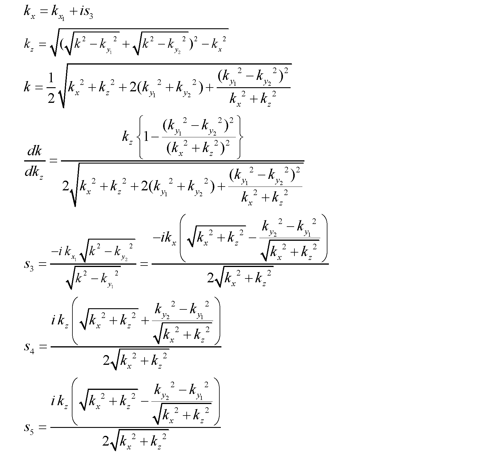
(x、y、z)は、映像化対象位置を示し、kx1、ky1及びky2は、前記散乱場関数のx1、y1及びy2に関する波数を示し、dは、前記距離を示し、Φ(xI、yI、yJ、zI、zJ、k)は、前記送信位置が(xI、yI、zI)で前記受信位置が(xI+d、yJ、zJ)である場合における前記計測データを示す
請求項12又は13に記載の映像化装置。 - 前記映像化装置は、前記送信器列として複数の送信器列、前記受信器列として複数の受信器列、又は、前記送信器列及び前記受信器列として複数の送信器列及び複数の受信器列を備える
請求項12又は13に記載の映像化装置。 - 前記情報処理回路は、

kx、s3、s4及びs5は、
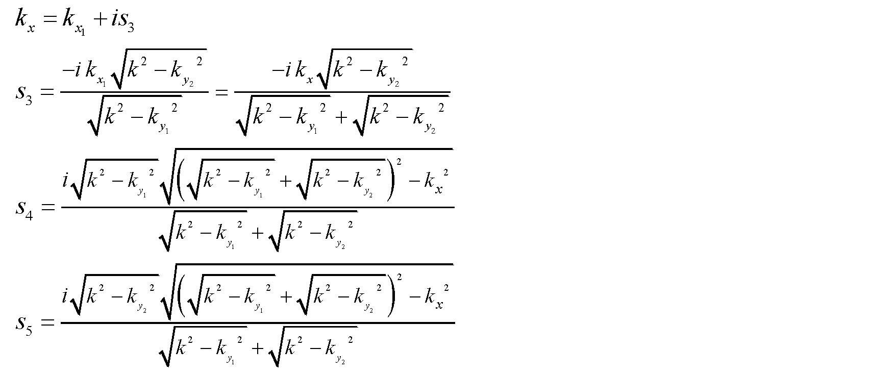
kx1、ky1及びky2は、前記散乱場関数のx1、y1及びy2に関する波数を示し、dは、前記距離を示し、Φ(xI、yI、yJ、zI、zJ、k)は、前記送信位置が(xI、yI、zI)で前記受信位置が(xI+d、yJ、zJ)である場合における前記計測データを示す
請求項17に記載の映像化装置。 - 前記情報処理回路は、前記送信器列及び前記受信器列に関する複数の組み合わせに対する複数の散乱場関数の合成を用いて前記映像化関数を導出し、
前記複数の散乱場関数のそれぞれは、前記散乱場関数に対応し、

kx、s3、s4及びs5は、
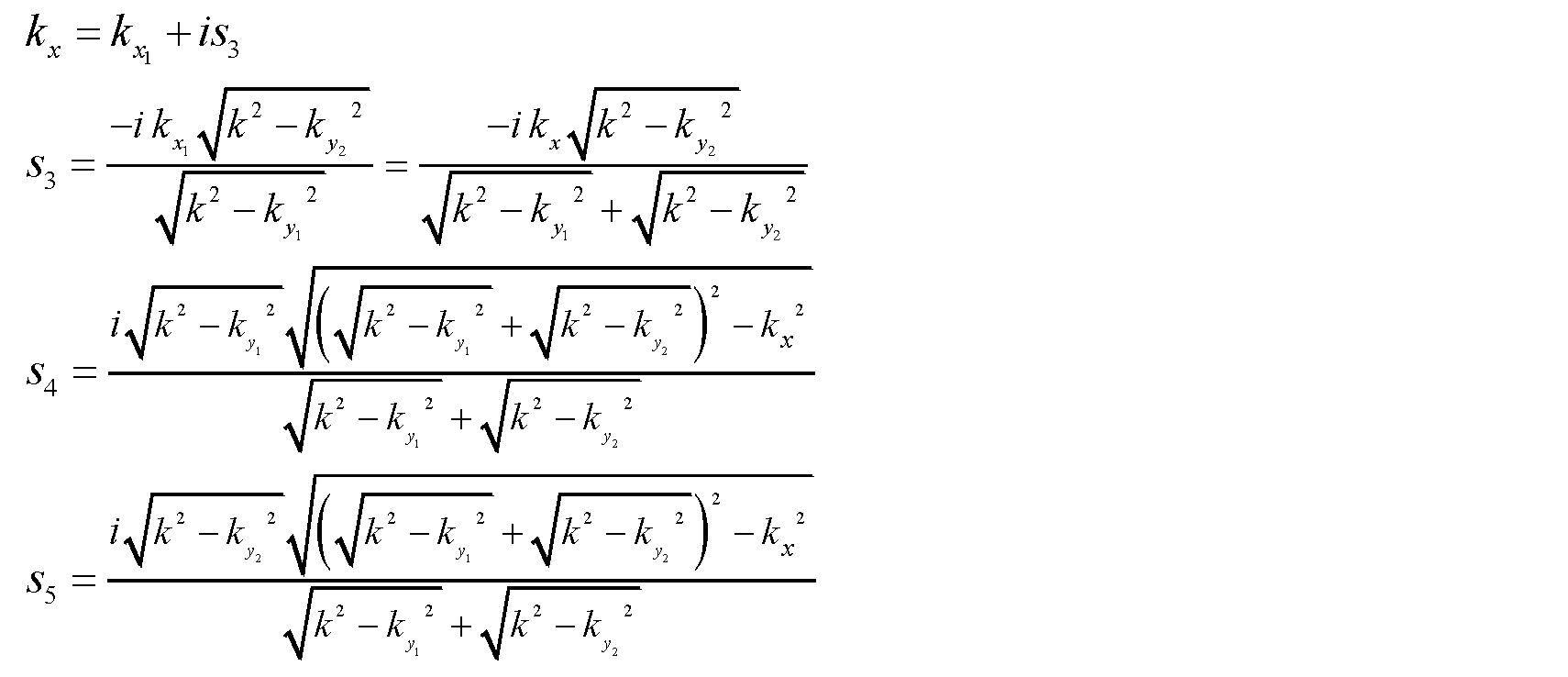
kx1、ky1及びky2は、前記散乱場関数のx1、y1及びy2に関する波数を示し、dは、前記距離を示し、Φ(xI、yI、yJ、zI、zJ、k)は、前記送信位置が(xI、yI、zI)で前記受信位置が(xI+d、yJ、zJ)である場合における前記計測データを示す
請求項17に記載の映像化装置。 - 前記情報処理回路は、前記領域において前記反射率に対応する誘電率が周波数依存性を有する場合、
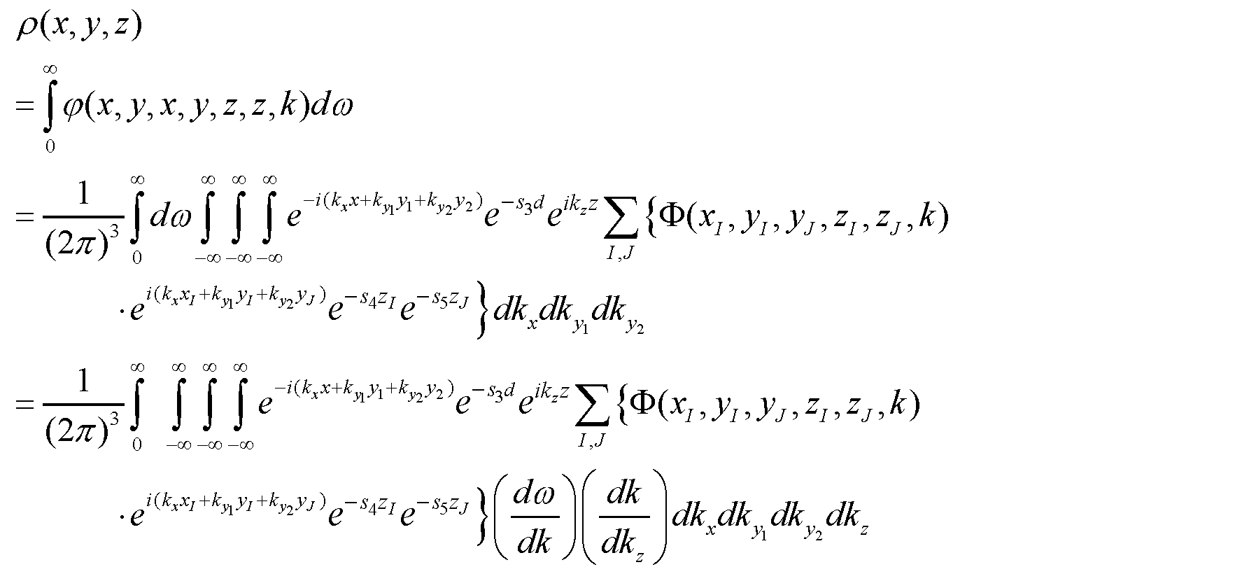
kx、kz、k、dk/dkz、dω/dk、s3、s4及びs5は、

(x、y、z)は、映像化対象位置を示し、kx1、ky1及びky2は、前記散乱場関数のx1、y1及びy2に関する波数を示し、dは、前記距離を示し、ωは、前記波動の角周波数を示し、c0は、真空中の前記波動の伝搬速度を示し、a、b及びαは、デバイ緩和に関するパラメータを示し、

請求項12又は13に記載の映像化装置。 - 直線上に配列された複数の送信器を含む送信器列の前記複数の送信器によって、計測対象の領域へ波動を送信するステップと、
前記複数の送信器が配列される直線に平行な別の直線上に配列された複数の受信器を含み、前記送信器列から間隔が設けられた受信器列の前記複数の受信器によって、前記領域から前記波動を受信するステップと、
前記複数の送信器と前記複数の受信器との全部又は一部の組み合わせによって得られる計測データ、及び、前記複数の送信器が配列される直線と前記複数の受信器が配列される直線との間の距離に従って、前記波動の散乱に関する散乱場関数に対応する映像化関数を導出し、前記映像化関数を用いて、前記領域内の物体に含まれる散乱体の構造を可視化するステップとを含む
映像化方法。
Priority Applications (10)
| Application Number | Priority Date | Filing Date | Title |
|---|---|---|---|
| BR112023025244A BR112023025244A2 (pt) | 2021-06-17 | 2022-06-14 | Dispositivo de formação de vídeo e método de formação de vídeo |
| CN202280038496.4A CN117501112A (zh) | 2021-06-17 | 2022-06-14 | 影像化装置及影像化方法 |
| EP22825005.6A EP4357766A4 (en) | 2021-06-17 | 2022-06-14 | VIDEO FORMING DEVICE AND METHOD |
| US18/568,490 US12487192B2 (en) | 2021-06-17 | 2022-06-14 | Imaging device and imaging method |
| KR1020237042622A KR20240021794A (ko) | 2021-06-17 | 2022-06-14 | 영상화 장치 및 영상화 방법 |
| JP2023530353A JP7822636B2 (ja) | 2021-06-17 | 2022-06-14 | 映像化装置及び映像化方法 |
| CA3222714A CA3222714A1 (en) | 2021-06-17 | 2022-06-14 | Video-forming device and video-forming method |
| AU2022292324A AU2022292324B2 (en) | 2021-06-17 | 2022-06-14 | Imaging device and imaging method |
| IL309050A IL309050A (en) | 2021-06-17 | 2022-06-14 | Imaging device and imaging method |
| SA523451915A SA523451915B1 (ar) | 2021-06-17 | 2023-12-12 | جهاز تصوير وطريقة تصوير |
Applications Claiming Priority (2)
| Application Number | Priority Date | Filing Date | Title |
|---|---|---|---|
| JP2021100909 | 2021-06-17 | ||
| JP2021-100909 | 2021-06-17 |
Publications (1)
| Publication Number | Publication Date |
|---|---|
| WO2022265017A1 true WO2022265017A1 (ja) | 2022-12-22 |
Family
ID=84527517
Family Applications (1)
| Application Number | Title | Priority Date | Filing Date |
|---|---|---|---|
| PCT/JP2022/023828 Ceased WO2022265017A1 (ja) | 2021-06-17 | 2022-06-14 | 映像化装置及び映像化方法 |
Country Status (12)
| Country | Link |
|---|---|
| US (1) | US12487192B2 (ja) |
| EP (1) | EP4357766A4 (ja) |
| JP (1) | JP7822636B2 (ja) |
| KR (1) | KR20240021794A (ja) |
| CN (1) | CN117501112A (ja) |
| AU (1) | AU2022292324B2 (ja) |
| BR (1) | BR112023025244A2 (ja) |
| CA (1) | CA3222714A1 (ja) |
| IL (1) | IL309050A (ja) |
| SA (1) | SA523451915B1 (ja) |
| TW (1) | TW202305400A (ja) |
| WO (1) | WO2022265017A1 (ja) |
Cited By (3)
| Publication number | Priority date | Publication date | Assignee | Title |
|---|---|---|---|---|
| WO2024190178A1 (ja) | 2023-03-10 | 2024-09-19 | 文俊 木村 | 映像化装置及び映像化方法 |
| WO2024209875A1 (ja) * | 2023-04-07 | 2024-10-10 | 文俊 木村 | 映像化装置及び映像化方法 |
| WO2024224849A1 (ja) * | 2023-04-24 | 2024-10-31 | 文俊 木村 | 映像化装置及び映像化方法 |
Citations (12)
| Publication number | Priority date | Publication date | Assignee | Title |
|---|---|---|---|---|
| JPS6266145A (ja) | 1985-09-06 | 1987-03-25 | シ−メンス、アクチエンゲゼルシヤフト | 誘電率分布検出方法 |
| JP2000514917A (ja) * | 1996-06-26 | 2000-11-07 | ユニバーシティー オブ ユタ リサーチ ファンデーション | 広帯域電磁ホログラフィック画像化方法 |
| US20040034307A1 (en) * | 1992-10-14 | 2004-02-19 | Johnson Steven A. | Apparatus and method for imaging objects with wavefields |
| WO2014125815A1 (ja) | 2013-02-12 | 2014-08-21 | 国立大学法人神戸大学 | 散乱トモグラフィ方法および散乱トモグラフィ装置 |
| WO2015136936A1 (ja) | 2014-03-12 | 2015-09-17 | 国立大学法人神戸大学 | 散乱トモグラフィ方法および散乱トモグラフィ装置 |
| WO2017057524A1 (ja) * | 2015-09-29 | 2017-04-06 | 国立大学法人神戸大学 | 画像化方法および画像化装置 |
| JP2017509416A (ja) * | 2014-03-31 | 2017-04-06 | コーニンクレッカ フィリップス エヌ ヴェKoninklijke Philips N.V. | 肋骨間空間を用いたコヒーレントな複合による音響撮像のためのシステム及び方法 |
| JP2018512985A (ja) * | 2015-04-01 | 2018-05-24 | ヴェラゾニックス,インコーポレーテッド | インパルス応答推定及び遡及的取得による符号化励起イメージングのための方法及びシステム |
| JP2019510593A (ja) * | 2016-01-18 | 2019-04-18 | メディカル ワイヤレス センシング リミテッド | マイクロ波トモグラフィシステム |
| JP2020031714A (ja) * | 2018-08-27 | 2020-03-05 | 国立大学法人静岡大学 | 診断装置、診断方法、診断プログラム |
| WO2021020387A1 (ja) | 2019-08-01 | 2021-02-04 | 株式会社 Integral Geometry Science | 散乱トモグラフィ装置及び散乱トモグラフィ方法 |
| WO2021053971A1 (ja) | 2019-09-17 | 2021-03-25 | 株式会社 Integral Geometry Science | 散乱トモグラフィ装置及び散乱トモグラフィ方法 |
Family Cites Families (4)
| Publication number | Priority date | Publication date | Assignee | Title |
|---|---|---|---|---|
| GB0915491D0 (en) * | 2009-09-04 | 2009-10-07 | Univ Keele | Electromagnetic tomography apparatuses and methods |
| FR3007145B1 (fr) * | 2013-06-18 | 2015-07-03 | Microwave Characterization Ct | Dispositif d'imagerie hyperfrequence portable, systeme comprenant un tel dispositif et procede d'imagerie correspondant |
| ES2729990T3 (es) * | 2016-01-20 | 2019-11-07 | Univ Pompeu Fabra | Sistema médico y dispositivo basado en tecnología de microondas para la prevención y el diagnóstico de enfermedades |
| CN107796837B (zh) * | 2017-10-09 | 2019-10-29 | 南京大学 | 一种成像装置、成像方法及成像系统 |
-
2022
- 2022-06-14 KR KR1020237042622A patent/KR20240021794A/ko active Pending
- 2022-06-14 CN CN202280038496.4A patent/CN117501112A/zh active Pending
- 2022-06-14 EP EP22825005.6A patent/EP4357766A4/en active Pending
- 2022-06-14 CA CA3222714A patent/CA3222714A1/en active Pending
- 2022-06-14 JP JP2023530353A patent/JP7822636B2/ja active Active
- 2022-06-14 WO PCT/JP2022/023828 patent/WO2022265017A1/ja not_active Ceased
- 2022-06-14 AU AU2022292324A patent/AU2022292324B2/en active Active
- 2022-06-14 IL IL309050A patent/IL309050A/en unknown
- 2022-06-14 BR BR112023025244A patent/BR112023025244A2/pt unknown
- 2022-06-14 US US18/568,490 patent/US12487192B2/en active Active
- 2022-06-16 TW TW111122495A patent/TW202305400A/zh unknown
-
2023
- 2023-12-12 SA SA523451915A patent/SA523451915B1/ar unknown
Patent Citations (12)
| Publication number | Priority date | Publication date | Assignee | Title |
|---|---|---|---|---|
| JPS6266145A (ja) | 1985-09-06 | 1987-03-25 | シ−メンス、アクチエンゲゼルシヤフト | 誘電率分布検出方法 |
| US20040034307A1 (en) * | 1992-10-14 | 2004-02-19 | Johnson Steven A. | Apparatus and method for imaging objects with wavefields |
| JP2000514917A (ja) * | 1996-06-26 | 2000-11-07 | ユニバーシティー オブ ユタ リサーチ ファンデーション | 広帯域電磁ホログラフィック画像化方法 |
| WO2014125815A1 (ja) | 2013-02-12 | 2014-08-21 | 国立大学法人神戸大学 | 散乱トモグラフィ方法および散乱トモグラフィ装置 |
| WO2015136936A1 (ja) | 2014-03-12 | 2015-09-17 | 国立大学法人神戸大学 | 散乱トモグラフィ方法および散乱トモグラフィ装置 |
| JP2017509416A (ja) * | 2014-03-31 | 2017-04-06 | コーニンクレッカ フィリップス エヌ ヴェKoninklijke Philips N.V. | 肋骨間空間を用いたコヒーレントな複合による音響撮像のためのシステム及び方法 |
| JP2018512985A (ja) * | 2015-04-01 | 2018-05-24 | ヴェラゾニックス,インコーポレーテッド | インパルス応答推定及び遡及的取得による符号化励起イメージングのための方法及びシステム |
| WO2017057524A1 (ja) * | 2015-09-29 | 2017-04-06 | 国立大学法人神戸大学 | 画像化方法および画像化装置 |
| JP2019510593A (ja) * | 2016-01-18 | 2019-04-18 | メディカル ワイヤレス センシング リミテッド | マイクロ波トモグラフィシステム |
| JP2020031714A (ja) * | 2018-08-27 | 2020-03-05 | 国立大学法人静岡大学 | 診断装置、診断方法、診断プログラム |
| WO2021020387A1 (ja) | 2019-08-01 | 2021-02-04 | 株式会社 Integral Geometry Science | 散乱トモグラフィ装置及び散乱トモグラフィ方法 |
| WO2021053971A1 (ja) | 2019-09-17 | 2021-03-25 | 株式会社 Integral Geometry Science | 散乱トモグラフィ装置及び散乱トモグラフィ方法 |
Non-Patent Citations (1)
| Title |
|---|
| See also references of EP4357766A4 |
Cited By (5)
| Publication number | Priority date | Publication date | Assignee | Title |
|---|---|---|---|---|
| WO2024190178A1 (ja) | 2023-03-10 | 2024-09-19 | 文俊 木村 | 映像化装置及び映像化方法 |
| KR20250155543A (ko) | 2023-03-10 | 2025-10-30 | 가부시키가이샤 케이-세오리 | 영상화 장치 및 영상화 방법 |
| EP4678117A1 (en) | 2023-03-10 | 2026-01-14 | K-Theory Inc. | Visualization device and visualization method |
| WO2024209875A1 (ja) * | 2023-04-07 | 2024-10-10 | 文俊 木村 | 映像化装置及び映像化方法 |
| WO2024224849A1 (ja) * | 2023-04-24 | 2024-10-31 | 文俊 木村 | 映像化装置及び映像化方法 |
Also Published As
| Publication number | Publication date |
|---|---|
| JP7822636B2 (ja) | 2026-03-03 |
| SA523451915B1 (ar) | 2025-05-21 |
| TW202305400A (zh) | 2023-02-01 |
| BR112023025244A2 (pt) | 2024-02-20 |
| EP4357766A1 (en) | 2024-04-24 |
| AU2022292324B2 (en) | 2025-12-04 |
| IL309050A (en) | 2024-02-01 |
| EP4357766A4 (en) | 2025-07-09 |
| CA3222714A1 (en) | 2022-12-22 |
| CN117501112A (zh) | 2024-02-02 |
| US20240295506A1 (en) | 2024-09-05 |
| KR20240021794A (ko) | 2024-02-19 |
| US12487192B2 (en) | 2025-12-02 |
| JPWO2022265017A1 (ja) | 2022-12-22 |
| AU2022292324A1 (en) | 2024-01-04 |
Similar Documents
| Publication | Publication Date | Title |
|---|---|---|
| JP7822636B2 (ja) | 映像化装置及び映像化方法 | |
| KR102826230B1 (ko) | 산란 토모그래피 장치 및 산란 토모그래피 방법 | |
| JP6557747B2 (ja) | 散乱トモグラフィ方法および散乱トモグラフィ装置 | |
| JP6938812B2 (ja) | データ処理方法及び計測装置 | |
| JP7813474B2 (ja) | 映像化装置及び映像化方法 | |
| EP4628933A1 (en) | Visualization device and visualization method | |
| KR20250155543A (ko) | 영상화 장치 및 영상화 방법 | |
| TWI916584B (zh) | 影像化裝置及影像化方法 | |
| RU2838982C2 (ru) | Устройство томографии на рассеяном излучении и способ томографии на рассеяном излучении | |
| EP4692773A1 (en) | Visualization device and visualization method | |
| WO2024161874A1 (ja) | 映像化装置及び映像化方法 | |
| KR20250174913A (ko) | 영상화 장치 및 영상화 방법 | |
| EA050659B1 (ru) | Устройство формирования изображений и способ формирования изображений |
Legal Events
| Date | Code | Title | Description |
|---|---|---|---|
| 121 | Ep: the epo has been informed by wipo that ep was designated in this application |
Ref document number: 22825005 Country of ref document: EP Kind code of ref document: A1 |
|
| WWE | Wipo information: entry into national phase |
Ref document number: 2023530353 Country of ref document: JP |
|
| WWE | Wipo information: entry into national phase |
Ref document number: 202280038496.4 Country of ref document: CN |
|
| WWE | Wipo information: entry into national phase |
Ref document number: 309050 Country of ref document: IL |
|
| WWE | Wipo information: entry into national phase |
Ref document number: 18568490 Country of ref document: US Ref document number: 2022292324 Country of ref document: AU Ref document number: AU2022292324 Country of ref document: AU |
|
| REG | Reference to national code |
Ref country code: BR Ref legal event code: B01A Ref document number: 112023025244 Country of ref document: BR |
|
| WWE | Wipo information: entry into national phase |
Ref document number: 3222714 Country of ref document: CA |
|
| WWE | Wipo information: entry into national phase |
Ref document number: 202393233 Country of ref document: EA |
|
| WWE | Wipo information: entry into national phase |
Ref document number: P6003263/2023 Country of ref document: AE |
|
| WWE | Wipo information: entry into national phase |
Ref document number: 523451915 Country of ref document: SA |
|
| ENP | Entry into the national phase |
Ref document number: 2022292324 Country of ref document: AU Date of ref document: 20220614 Kind code of ref document: A |
|
| WWE | Wipo information: entry into national phase |
Ref document number: 202447003255 Country of ref document: IN Ref document number: 2022825005 Country of ref document: EP |
|
| NENP | Non-entry into the national phase |
Ref country code: DE |
|
| ENP | Entry into the national phase |
Ref document number: 2022825005 Country of ref document: EP Effective date: 20240117 |
|
| ENP | Entry into the national phase |
Ref document number: 112023025244 Country of ref document: BR Kind code of ref document: A2 Effective date: 20231130 |
|
| WWE | Wipo information: entry into national phase |
Ref document number: 523451915 Country of ref document: SA |
|
| WWE | Wipo information: entry into national phase |
Ref document number: 523451915 Country of ref document: SA |
|
| WWG | Wipo information: grant in national office |
Ref document number: 523451915 Country of ref document: SA |