WO2023018137A1 - 안테나를 포함하는 전자 장치 - Google Patents
안테나를 포함하는 전자 장치 Download PDFInfo
- Publication number
- WO2023018137A1 WO2023018137A1 PCT/KR2022/011755 KR2022011755W WO2023018137A1 WO 2023018137 A1 WO2023018137 A1 WO 2023018137A1 KR 2022011755 W KR2022011755 W KR 2022011755W WO 2023018137 A1 WO2023018137 A1 WO 2023018137A1
- Authority
- WO
- WIPO (PCT)
- Prior art keywords
- conductive part
- electronic device
- switching circuit
- sensor
- conductive
- Prior art date
- Legal status (The legal status is an assumption and is not a legal conclusion. Google has not performed a legal analysis and makes no representation as to the accuracy of the status listed.)
- Ceased
Links
Images




Classifications
-
- H—ELECTRICITY
- H01—ELECTRIC ELEMENTS
- H01Q—ANTENNAS, i.e. RADIO AERIALS
- H01Q1/00—Details of, or arrangements associated with, antennas
- H01Q1/12—Supports; Mounting means
- H01Q1/22—Supports; Mounting means by structural association with other equipment or articles
- H01Q1/24—Supports; Mounting means by structural association with other equipment or articles with receiving set
- H01Q1/241—Supports; Mounting means by structural association with other equipment or articles with receiving set used in mobile communications, e.g. GSM
- H01Q1/242—Supports; Mounting means by structural association with other equipment or articles with receiving set used in mobile communications, e.g. GSM specially adapted for hand-held use
- H01Q1/243—Supports; Mounting means by structural association with other equipment or articles with receiving set used in mobile communications, e.g. GSM specially adapted for hand-held use with built-in antennas
-
- G—PHYSICS
- G06—COMPUTING OR CALCULATING; COUNTING
- G06F—ELECTRIC DIGITAL DATA PROCESSING
- G06F1/00—Details not covered by groups G06F3/00 - G06F13/00 and G06F21/00
- G06F1/16—Constructional details or arrangements
-
- G—PHYSICS
- G06—COMPUTING OR CALCULATING; COUNTING
- G06F—ELECTRIC DIGITAL DATA PROCESSING
- G06F1/00—Details not covered by groups G06F3/00 - G06F13/00 and G06F21/00
- G06F1/16—Constructional details or arrangements
- G06F1/1613—Constructional details or arrangements for portable computers
- G06F1/1633—Constructional details or arrangements of portable computers not specific to the type of enclosures covered by groups G06F1/1615 - G06F1/1626
- G06F1/1637—Details related to the display arrangement, including those related to the mounting of the display in the housing
- G06F1/1641—Details related to the display arrangement, including those related to the mounting of the display in the housing the display being formed by a plurality of foldable display components
-
- G—PHYSICS
- G09—EDUCATION; CRYPTOGRAPHY; DISPLAY; ADVERTISING; SEALS
- G09F—DISPLAYING; ADVERTISING; SIGNS; LABELS OR NAME-PLATES; SEALS
- G09F9/00—Indicating arrangements for variable information in which the information is built-up on a support by selection or combination of individual elements
- G09F9/30—Indicating arrangements for variable information in which the information is built-up on a support by selection or combination of individual elements in which the desired character or characters are formed by combining individual elements
-
- G—PHYSICS
- G09—EDUCATION; CRYPTOGRAPHY; DISPLAY; ADVERTISING; SEALS
- G09F—DISPLAYING; ADVERTISING; SIGNS; LABELS OR NAME-PLATES; SEALS
- G09F9/00—Indicating arrangements for variable information in which the information is built-up on a support by selection or combination of individual elements
- G09F9/30—Indicating arrangements for variable information in which the information is built-up on a support by selection or combination of individual elements in which the desired character or characters are formed by combining individual elements
- G09F9/301—Indicating arrangements for variable information in which the information is built-up on a support by selection or combination of individual elements in which the desired character or characters are formed by combining individual elements flexible foldable or roll-able electronic displays, e.g. thin LCD, OLED
-
- H—ELECTRICITY
- H01—ELECTRIC ELEMENTS
- H01Q—ANTENNAS, i.e. RADIO AERIALS
- H01Q1/00—Details of, or arrangements associated with, antennas
- H01Q1/12—Supports; Mounting means
- H01Q1/22—Supports; Mounting means by structural association with other equipment or articles
- H01Q1/24—Supports; Mounting means by structural association with other equipment or articles with receiving set
-
- H—ELECTRICITY
- H01—ELECTRIC ELEMENTS
- H01Q—ANTENNAS, i.e. RADIO AERIALS
- H01Q1/00—Details of, or arrangements associated with, antennas
- H01Q1/36—Structural form of radiating elements, e.g. cone, spiral, umbrella; Particular materials used therewith
- H01Q1/38—Structural form of radiating elements, e.g. cone, spiral, umbrella; Particular materials used therewith formed by a conductive layer on an insulating support
Definitions
- the electronic device may include a metal exterior member, and the metal exterior member may provide a luxurious design unique to metal and improve durability.
- An electronic device may utilize a metal exterior member as an antenna.
- an external dielectric substance such as a hand carrying the electronic device may affect transmission and reception of radio waves.
- Various embodiments of the present disclosure may provide an electronic device including an antenna for reducing performance deterioration of transmission and reception of radio waves due to an external dielectric.
- an electronic device may include a foldable housing, a communication circuit, a first sensor IC, a second sensor IC, a first switching circuit, a processor, and a memory.
- the foldable housing includes a first housing hingedly connected to the second housing, a first side member disposed on a side surface of the first housing and including a plurality of first conductive parts, and a side surface of the second housing, A second side member including a plurality of second conductive parts may be included.
- the communication circuit may be electrically connected to a first conductive part of the first plurality of conductive parts and configured to transmit and/or receive a signal of a selected or specified frequency band.
- the first sensor IC may be electrically connected to at least one of the plurality of first conductive parts and measure capacitance.
- the second sensor IC may be electrically connected to at least one of the plurality of second conductive parts and measure capacitance.
- the first switching circuit may be electrically connected to the first conductive part and the second conductive part among the plurality of first conductive parts.
- the memory may store instructions that, when executed, cause the processor to perform a plurality of operations.
- the plurality of operations may include an operation of controlling the first switching circuit, wherein the capacitance measured by the first sensor IC and the second sensor IC when the foldable housing is in a folded state Based on at least one of the capacitances measured by , the first conductive part and the second conductive part may be electrically connected.
- An electronic device including an antenna uses a plurality of grip sensors (eg, a plurality of capacitance sensors) to check a spatial or positional relationship between an electronic device and an external dielectric such as a hand, and , Based on the confirmation result, at least a part of the metal exterior member is variably used as an antenna radiator (or radiating part) to secure radio transmission and reception performance in the frequency band used, so that specified performance can be secured in various usage environments.
- a plurality of grip sensors eg, a plurality of capacitance sensors
- FIG. 1 is a block diagram of an electronic device in a networked environment, in one embodiment.
- FIG. 2 is diagrams illustrating an electronic device in an unfolded state, in one embodiment.
- FIGS. 3 are diagrams illustrating an electronic device in a folded state, in one embodiment.
- FIG. 4 is a view showing a first side member and a second side member in one embodiment.
- 5 is a block diagram of an electronic device, in one embodiment.
- FIG. 6 is, for example, a perspective view of a state in which a folded electronic device is carried by a user's hand.
- FIG. 7 is a block diagram of an electronic device, in one embodiment.
- FIG. 8 is a block diagram of a first antenna implemented when an electronic device in a folded state is in a free state, in an embodiment.
- FIG. 9 is a block diagram of a second antenna implemented when an electronic device in a folded state is in a free state, in another embodiment.
- FIG. 10 is a block diagram of a third antenna implemented when an electronic device in a folded state is in a second use condition, in an embodiment.
- 11 and 12 are, for example, graphs showing antenna radiation performance for the first antenna of FIG. 8 according to an embodiment and antenna radiation performance for an antenna according to a comparison example.
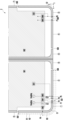
- FIG. 13 13, 14, 15, 16, 17, and 18 are diagrams illustrating another embodiment in which the embodiment of FIG. 5 is modified or changed according to various embodiments.
- FIG. 1 is a block diagram of an electronic device 101 within a networked environment 100, in one embodiment.
- an electronic device 101 communicates with an external electronic device 102 through a first network 198 (eg, a short-range wireless communication network) or a second network 199. ) (eg, a long-distance wireless communication network) may communicate with at least one of the external electronic device 104 or the server 108 .
- the electronic device 101 may communicate with the external electronic device 104 through the server 108 .
- the electronic device 101 includes a processor 120, a memory 130, an input module 150, a sound output module 155, a display module 160, an audio module 170, a sensor module 176, and an interface 177.
- connection terminal 178 may be included in the electronic device 101.
- at least one of these components eg, the connection terminal 178, may be omitted or one or more other components may be added.
- some of these components may be implemented as a single integrated circuitry.
- the sensor module 176, the camera module 180, or the antenna module 197 may be implemented by being embedded in one component (eg, the display module 160).
- the processor 120 for example, executes software (eg, the program 140) to cause at least one other component (eg, hardware or software component) of the electronic device 101 connected to the processor 120. It can control and perform various data processing or calculations. As at least part of data processing or operation, processor 120 loads instructions or data received from other components (eg, sensor module 176 or communication module 190) into volatile memory 132 and , the command or data stored in the volatile memory 132 may be processed, and the resulting data may be stored in the non-volatile memory 134.
- software eg, the program 140
- processor 120 loads instructions or data received from other components (eg, sensor module 176 or communication module 190) into volatile memory 132 and , the command or data stored in the volatile memory 132 may be processed, and the resulting data may be stored in the non-volatile memory 134.
- the processor 120 may include a main processor 121 (eg, a central processing unit (CPU) or an application processor (AP)) or a secondary processor 123 (eg, a central processing unit (CPU)) or an auxiliary processor 123 (eg, which may be operated independently or together). : Graphics processing unit (GPU), neural processing unit (NPU), image signal processor (ISP), sensor hub processor, or communication processor (CP) )) may be included. Additionally or alternatively, the secondary processor 123 may use less power than the main processor 121 or may be configured to be specialized for a designated function. The secondary processor 123 may be implemented separately from or as part of the main processor 121 .
- a main processor 121 eg, a central processing unit (CPU) or an application processor (AP)
- a secondary processor 123 eg, a central processing unit (CPU)
- auxiliary processor 123 eg, which may be operated independently or together.
- GPU Graphics processing unit
- NPU neural processing unit
- ISP
- the secondary processor 123 may, for example, take the place of the main processor 121 while the main processor 121 is in an inactive (eg, sleep) state, or the main processor 121 is active (eg, running an application). ) state, together with the main processor 121, at least one of the components of the electronic device 101 (eg, the display module 160, the sensor module 176, or the communication module 190) It is possible to control at least some of the related functions or states.
- Co-processor 123 eg, image signal processor (ISP) or communication processor (CP)
- ISP image signal processor
- CP communication processor
- the auxiliary processor 123 may include a specialized hardware structure to process an artificial intelligence model.
- AI models can be created through machine learning. Such learning may be performed, for example, in the electronic device 101 itself where the artificial intelligence model is performed, or through a separate server (eg, the server 108).
- the learning algorithm may include, for example, supervised learning, unsupervised learning, semi-supervised learning, or reinforcement learning, but the foregoing example not limited to
- An artificial intelligence model may include a plurality of artificial neural network layers.
- Artificial neural networks include deep neural networks (DNNs), convolutional neural networks (CNNs), recurrent neural networks (RNNs), restricted Boltzmann machines (RBMs), deep belief networks (DBNs), bidirectional recurrent DNNs (BRDNNs), and deep neural networks. It may be any one of deep Q-networks or a combination of two or more of the above, but is not limited to the above example. In addition to hardware structures, AI models may additionally or alternatively include software structures.
- the memory 130 may store various data used by at least one component (eg, the processor 120 or the sensor module 176) of the electronic device 101 .
- the various data may include, for example, input data or output data for software (eg, program 140) and commands related thereto.
- Memory 130 may include volatile memory 132 and/or non-volatile memory 134 .
- the program 140 may be stored as software in the memory 130 and may include, for example, an operating system 142 , middleware 144 , and/or applications 146 .
- the input module 150 may receive a command or data to be used for other components (eg, the processor 120) of the electronic device 101 from the outside of the electronic device 101 (eg, a user).
- the input module 150 may include, for example, a microphone, a mouse, a keyboard, a key (eg, a button), or a digital pen (eg, a stylus pen).
- the sound output module 155 may output sound signals to the outside of the electronic device 101 .
- the sound output module 155 may include, for example, a speaker or a receiver.
- the speaker can be used for general purposes such as playing multimedia or recording, and the receiver can be used for incoming calls.
- the receiver may be implemented separately from the speaker or as part of it.
- the display module 160 may visually provide information to the outside of the electronic device 101 (eg, a user).
- the display module 160 may include, for example, a display, a hologram device, or a projector and a control circuit for controlling the device.
- the display module 160 may include a touch circuit configured to detect a touch (eg, a touch sensor) or a sensor circuit configured to measure the intensity of force generated by the touch (eg, a pressure sensor).
- the audio module 170 may convert sound into an electrical signal or vice versa.
- the audio module 170 acquires sound through the input module 150, the sound output module 155, or an external electronic device connected directly or wirelessly to the electronic device 101 (eg, the external electronic device 102). You can output sound through (e.g. speakers or headphones).
- the sensor module 176 detects an operating state (eg, power or temperature) of the electronic device 101 or an external environmental state (eg, a user state), and generates an electrical signal or data value corresponding to the detected state. can do.
- the sensor module 176 may include, for example, a gesture sensor, a gyro sensor, an air pressure sensor, a magnetic sensor, an acceleration sensor, a grip sensor, a proximity sensor, a color sensor, an IR (infrared) sensor, a bio sensor, a temperature sensor, a humidity sensor, Alternatively, an illuminance sensor may be included.
- the interface 177 may support one or more specified protocols that may be used to directly or wirelessly connect the electronic device 101 to an external electronic device (eg, the external electronic device 102).
- the interface 177 may include, for example, a high-definition multimedia interface (HDMI), a universal serial bus (USB) interface, an SD card interface, and/or an audio interface.
- HDMI high-definition multimedia interface
- USB universal serial bus
- SD card interface Secure Digital Card
- the connection terminal 178 may include a connector through which the electronic device 101 may be physically connected to an external electronic device (eg, the external electronic device 102).
- the connection terminal 178 may include, for example, an HDMI connector, a USB connector, an SD card connector, and/or an audio connector (eg, a headphone connector).
- the haptic module 179 may convert electrical signals into mechanical stimuli (eg, vibration or motion) or electrical stimuli that a user may perceive through tactile or kinesthetic senses.
- the haptic module 179 may include, for example, a motor, a piezoelectric element, or an electrical stimulation device.
- the camera module 180 may capture still images and moving images.
- the camera module 180 may include one or more lenses, image sensors, image signal processors (ISPs), or flashes.
- ISPs image signal processors
- the power management module 188 may manage power supplied to or consumed by the electronic device 101 .
- the power management module 188 may be implemented as at least part of a power management integrated circuit (PMIC), for example.
- PMIC power management integrated circuit
- the battery 189 may supply power to at least one component of the electronic device 101 .
- the battery 189 may include, for example, a non-rechargeable primary cell, a rechargeable secondary cell, and/or a fuel cell.
- the communication module 190 is a direct (eg, wired) communication channel or wireless communication between the electronic device 101 and an external electronic device (eg, the external electronic device 102, the external electronic device 104, or the server 108). Establishing a channel and performing communication through the established communication channel can be supported.
- the communication module 190 may include one or more communication processors (CPs) that operate independently of the processor 120 (eg, an application processor (AP)) and support direct (eg, wired) communication or wireless communication. .
- CPs communication processors
- AP application processor
- the communication module 190 may be a wireless communication module 192 (eg, a cellular communication module, a short-range wireless communication module, or a global navigation satellite system (GNSS) communication module) or a wired communication module 194 (eg, a local area network (LAN)). ) communication module, or power line communication module).
- a wireless communication module 192 eg, a cellular communication module, a short-range wireless communication module, or a global navigation satellite system (GNSS) communication module
- GNSS global navigation satellite system
- wired communication module 194 eg, a local area network (LAN)
- LAN local area network
- the corresponding communication module is a first network 198 (eg, a short-range communication network such as Bluetooth (BLUETOOTH), wireless fidelity (WiFi) direct, or IR data association (IrDA)) or a second network 199 (eg, a legacy cellular network, a 5 th generation (5G) network, a next-generation communication network, the Internet, or a telecommunication network such as a computer network (eg, a LAN or WAN)) to communicate with the external electronic device 104 .
- a first network 198 eg, a short-range communication network such as Bluetooth (BLUETOOTH), wireless fidelity (WiFi) direct, or IR data association (IrDA)
- a second network 199 eg, a legacy cellular network, a 5 th generation (5G) network, a next-generation communication network, the Internet, or a telecommunication network such as a computer network (eg, a LAN or WAN)
- a telecommunication network
- the wireless communication module 192 communicates with the first network 198 or the second network 199 using subscriber information (eg, International Mobile Subscriber Identifier (IMSI)) stored in the subscriber identity module (SIM) 196.
- subscriber information eg, International Mobile Subscriber Identifier (IMSI)
- SIM subscriber identity module
- the electronic device 101 may be identified or authenticated within the network.
- the wireless communication module 192 may support a 5G network after a 4th generation (4G) network and a next-generation communication technology, such as NR access technology (new radio access technology).
- NR access technologies include high-speed transmission of high-capacity data (i.e., enhanced mobile broadband (eMBB)), minimization of terminal power and access of multiple terminals (massive machine type communications (mMTC)), or high reliability and low latency (ultra-reliable communications (URLLC)). and low-latency communications)).
- eMBB enhanced mobile broadband
- mMTC massive machine type communications
- URLLC ultra-reliable communications
- the wireless communication module 192 may support a high frequency band (eg, mmWave band) to achieve a high data rate, for example.
- the wireless communication module 192 uses various technologies for securing performance in a high frequency band, such as beamforming, massive multiple-input and multiple-output (MIMO), and full-dimensional multiplexing. Technologies such as input/output (full-dimensional MIMO (FD-MIMO)), array antenna, analog beam-forming, or large-scale antenna may be supported.
- the wireless communication module 192 may support various requirements defined for the electronic device 101, an external electronic device (eg, the external electronic device 104), or a network system (eg, the second network 199).
- the wireless communication module 192 is configured to achieve peak data rate (eg, 20 Gbps or more) for realizing eMBB, loss coverage (eg, 164 dB or less) for realizing mMTC, or U-U- for realizing URLLC.
- Plane latency eg, downlink (DL) and uplink (UL) 0.5 ms or less, or round trip 1 ms or less
- DL downlink
- UL uplink
- round trip 1 ms or less can be supported.
- the antenna module 197 may transmit or receive signals or power to the outside (eg, an external electronic device).
- the antenna module 197 may include an antenna including a radiator including a conductor or a conductive pattern formed on a substrate (eg, a printed circuit board (PCB)).
- the antenna module 197 may include a plurality of antennas (eg, an antenna array). In this case, at least one antenna suitable for a communication method used in a communication network such as the first network 198 or the second network 199 is selected from the plurality of antennas by the communication module 190, for example. can be chosen A signal or power may be transmitted or received between the communication module 190 and an external electronic device through the selected at least one antenna.
- other components eg, a radio frequency integrated circuit (RFIC) may be additionally formed as a part of the antenna module 197 .
- RFIC radio frequency integrated circuit
- the antenna module 197 may form a mmWave antenna module.
- the mmWave antenna module is disposed on or adjacent to a printed circuit board (PCB), a first surface (eg, bottom surface) of the printed circuit board, and has a designated high frequency band (eg, mmWave band). and a plurality of antennas (eg, a top surface or a side surface) disposed on or adjacent to a second surface (eg, a top surface or a side surface) of the printed circuit board and capable of transmitting or receiving signals of the designated high frequency band. array antenna).
- PCB printed circuit board
- a first surface eg, bottom surface
- a designated high frequency band eg, mmWave band
- a plurality of antennas eg, a top surface or a side surface
- a second surface eg, a top surface or a side surface
- peripheral devices eg, a bus, general purpose input and output (GPIO), serial peripheral interface (SPI), or mobile industry processor interface (MIPI)
- signal e.g. commands or data
- Commands or data may be transmitted or received between the electronic device 101 and the external electronic device 104 through the server 108 connected to the second network 199 .
- Each of the external electronic devices 102 or 104 may be the same as or different from the electronic device 101 .
- All or part of the operations executed in the electronic device 101 may be executed in one or more external electronic devices among the external electronic devices 102 , 104 , or 108 .
- the electronic device 101 when the electronic device 101 needs to perform a certain function or service automatically or in response to a request from a user or another device, the electronic device 101 instead of executing the function or service by itself.
- one or more external electronic devices may be requested to perform the function or at least part of the service.
- One or more external electronic devices receiving the request may execute at least a part of the requested function or service or an additional function or service related to the request, and deliver the execution result to the electronic device 101 .
- the electronic device 101 may provide the result as at least part of a response to the request as it is or additionally processed.
- cloud computing distributed computing, mobile edge computing (MEC), or client-server computing technology may be used.
- the electronic device 101 may provide an ultra-low delay service using, for example, distributed computing or mobile edge computing (MEC).
- the external electronic device 104 may include an internet of things (IoT) device.
- Server 108 may be an intelligent server using machine learning and/or neural networks.
- the external electronic device 104 or server 108 may be included in the second network 199 .
- the electronic device 101 may be applied to intelligent services (eg, smart home, smart city, smart car, or health care) based on 5G communication technology and IoT-related technology.
- An electronic device may be various types of devices.
- the electronic device may include a portable communication device (eg, smart phone), a computer device, a portable multimedia device, a portable medical device, a camera, a wearable device, or a home appliance.
- a portable communication device eg, smart phone
- a computer device e.g., a personal computer
- a portable multimedia device e.g., a personal computer
- a portable medical device e.g., a portable medical device
- camera e.g., a camera
- a wearable device e.g., a portable medical device
- a home appliance e.g., a portable medical device, or a portable medical device.
- the electronic device is not limited to the above devices.
- Terms such as “first”, “second”, or “first” or “secondary” may simply be used to distinguish that component from other corresponding components, and may refer to that component in other respects (eg, importance or order) is not limited.
- An element e.g., a first component
- is “coupled” or “connected” to another element e.g., a second component
- the terms “functionally” or “communicatively” When referred to as “tied”, it means that the certain component may be connected to the other component directly (eg, by wire), wirelessly, or through a third component.
- module may include units implemented in hardware, software, or firmware, and may be used interchangeably with terms such as, for example, logic, logical blocks, components, or circuits.
- a module may be an integrally constructed component or a minimal unit of components or a portion thereof that performs one or more functions.
- the module may be implemented in the form of an application-specific integrated circuit (ASIC).
- ASIC application-specific integrated circuit
- a storage medium eg, internal memory 136 or external memory 138
- a machine eg, electronic device 101
- a processor eg, the processor 120
- a device eg, the electronic device 101
- the one or more instructions may include code generated by a compiler or code executable by an interpreter.
- the device-readable storage medium may be provided in the form of a non-transitory storage medium.
- the storage medium is a tangible device and does not contain a signal (e.g. electromagnetic wave), and this term refers to the case where data is stored semi-permanently in the storage medium. It does not discriminate when it is temporarily stored.
- a signal e.g. electromagnetic wave
- the method according to an embodiment of this document may be included and provided in a computer program product.
- Computer program products may be traded between sellers and buyers as commodities.
- a computer program product is distributed in the form of a machine-readable storage medium (eg CD-ROM (compact disc read only memory)), or through an application store (eg PLAYSTORE TM ) or on two user devices (eg CD-ROM). : can be distributed (e.g., downloaded or uploaded) online, directly between smart phones.
- at least part of the computer program product may be temporarily stored or temporarily created in a device-readable storage medium such as a manufacturer's server, an application store server, or a relay server's memory.
- Each component (eg, module or program) of the components described above may include a single entity or a plurality of entities. One or more components or operations among the aforementioned corresponding components may be omitted, or one or more other components or operations may be added. Alternatively or additionally, a plurality of components (eg modules or programs) may be integrated into a single component. In this case, the integrated component may perform one or more functions of each of the plurality of components identically or similarly to those performed by the corresponding component among the plurality of components prior to the integration. .
- the actions performed by a module, program, or other component may be executed sequentially, in parallel, iteratively, or heuristically, or one or more of the operations may be executed in a different order, omitted, or one or more other operations. may be added.
- FIGS. 2 are diagrams illustrating the electronic device 2 in a flat or unfolded state, in one embodiment.
- 3 are diagrams showing the electronic device 2 in a folded state (or in a folded state), in one embodiment.
- the electronic device 2 may include a foldable housing 20 .
- the foldable housing 20 may include a first surface 20A of the electronic device 2 and a second surface 20B of the electronic device 2 positioned opposite to the first surface 20A. there is.
- the foldable housing 20 may include a first side surface 20C and a second side surface 20D of the electronic device 2 that at least partially surround a space between the first surface 20A and the second surface 20B.
- the first surface 20A may include a first cover area a, a second cover area b, and a folding cover area F between the first cover area a and the second cover area b.
- the first surface 20A may be substantially flat, and the first cover area a, the second cover area b, and the folding cover area F may be substantially flat. can be directed in the same direction. Also, the first cover area a, the second cover area b, and the folding cover area F may form one substantially continuous surface.
- the second surface 20B may include a third cover area c and a fourth cover area d.
- the third cover area c is located on the opposite side of the first surface 20A to the first cover area a and may face in the opposite direction to the first cover area a.
- the fourth cover area d is located on the opposite side of the first surface 20A to the second cover area b and may face in the opposite direction to the second cover area b.
- the foldable housing 20 may be implemented in an in-folding structure in which the first surface 20A is folded inward.
- the folding cover area F in the unfolded state of the foldable housing 20 (see FIG. 2 ), the folding cover area F is disposed in a flat shape, and the first cover area a and the second cover area b are about It can form an angle of 180 degrees.
- the folding cover area F In the folded state (see FIG. 3) of the foldable housing 20, the folding cover area F is disposed in a curved shape, and the first cover area a and the second cover area b are at an angle of about 180 degrees and can form different angles.
- the folded state may include a fully folded state or an intermediate state.
- the completely folded state see FIG.
- the electronic device 2 may be implemented in an out-folding structure in which the first surface 20A (or screen) is folded outward.
- the foldable housing 20 may include a front cover (eg, a window) 201 providing at least a portion of the first surface 20A.
- the flexible display 30 may overlap the front cover 201 at least partially and be positioned in the internal space of the electronic device 2 .
- the front cover 201 may protect the flexible display 30 from the outside and may be substantially transparent. Light output from the flexible display 30 may pass through the front cover 201 and proceed to the outside.
- the flexible display 30 includes, for example, a first display area (or first active area) overlapping the first cover area a of the first surface 20A, and a second area of the first surface 20A.
- the screen may refer to an area capable of expressing an image in a device including the flexible display 30 and the front cover 201, and for example, the display area of the flexible display 30 and the front cover 201 overlapping the display area may include an area of
- the front cover 201 is a component included in the flexible display 30 and may be integrally formed with the flexible display 30 .
- the user can use the larger flexible display 30 when the electronic device 2 is unfolded.
- the user may fold the electronic device 2 as shown in FIG. 4 .
- the x-dimension is approximately half the size of the electronic device 2 when it is unfolded.
- the flexible display 30 may not be visible to the user.
- the front cover 201 may be implemented in a thin film form to have flexibility.
- the front cover 201 may include, for example, a plastic film (eg, polyimide film) or thin glass (eg, ultra-thin glass (UTG)).
- the front The cover 201 may include a plurality of layers, for example, the front cover 201 may be made of plastic film or thin glass and various polymer materials (eg, polyester (PET), polyimide (PI), or thermoplastic (TPU)). It may be a form in which a coating layer or a protective layer of polyurethane)) is disposed.
- PET polyester
- PI polyimide
- TPU thermoplastic
- the foldable housing 20 includes a first housing (or first housing part or first housing structure) 21, a second housing (or second housing part or second housing structure) ( 22), and/or a hinge assembly (or hinge structure) (not shown).
- the first housing 21 and the second housing 22 are hingeably connected to each other.
- the first housing 21 and the second housing 22 are connected by a hinge assembly, and may be mutually rotatable based on a folding axis A of the foldable housing 20 (eg, a rotational axis of the hinge assembly).
- the first housing 21 provides at least a portion of the first cover portion of the front cover 201 and the third cover area c of the second surface 20B located on one side of the folding axis A.
- the first cover portion of the front cover 201 may include, for example, a first folding cover area F1 located on one side of the first cover area a and the folding cover area F with respect to the folding axis A. ) can be provided.
- the second housing 22 provides at least a portion of the second cover portion of the front cover 201 and the fourth cover area d of the second surface 20B located on one side of the folding axis A.
- a second side member (or side bezel structure) 222 providing a second side surface 20D by at least partially enclosing the rear cover 221 and the space between the second cover part and the second rear cover 221 can include
- the second cover portion of the front cover 201 may include, for example, a second folding cover area F2 located on the other side with respect to the folding axis A of the second cover area b and the folding cover area F. ) can be provided.
- the first side member 212 and the second side member 222 may overlap and align at least partially.
- the first side member 212 and/or the second side member 222 may be, for example, ceramic, polymer, metal (eg, aluminum, stainless steel, or magnesium), or a combination of at least two of the foregoing. can be formed by The first side member 212 and/or the second side member 222 may be, for example, titanium, an amorphous alloy, a metal-ceramic composite material (eg, cermet), stainless steel, magnesium, a magnesium alloy, It may include various metal materials such as aluminum, aluminum alloy, zinc alloy, or copper alloy.
- the first rear cover 211 and/or the second rear cover 221 may be substantially opaque.
- the first rear cover 211 and/or the second rear cover 221 may be, for example, coated or tinted glass, ceramic, polymer, metal (eg aluminum, stainless steel, or magnesium), or any of the foregoing materials. It may be formed by a combination of at least two of them.
- the first rear cover 211 or the second rear cover 221 is, for example, a plate of various materials such as transparent glass, ceramic, or polymer, and at least one coating layer disposed on the plate using a coating.
- the first rear cover 211 or the second rear cover 221 may include a plate made of various materials such as transparent glass, ceramic, or polymer, and a film having various visual effects attached to the plate (eg, decorations). A film (decoration film) may be included.
- the first rear cover 211 and the first side member 212 may be integrally formed and may include the same material.
- the second rear cover 221 and the second side member 222 may be integrally formed and may include the same material.
- the hinge assembly may include the hinge housing 40 .
- the hinge housing 40 is an element that covers at least one hinge connecting the first housing 21 and the second housing 22, and may be referred to as a hinge cover in some embodiments.
- the hinge housing 400 opens the gap B between the first housing 21 and the second housing 22
- the inside of the electronic device 2 may be covered so as not to be exposed.
- the gap B may be substantially absent, and the hinge housing 40 is formed between the first housing 21 and the second housing 22. It may be covered by and not exposed to the outside.
- the hinge housing 40 may be partially exposed between the first housing 21 and the second housing 22 .
- the hinge housing 40 may be more exposed in the folded state of FIG. 3 than in the intermediate state.
- the foldable housing 20 has a structure (e.g., providing at least a portion of the first side 20A, the second side 20B, the first side 20C, and the second side 20D).
- a foldable housing structure or a foldable housing assembly may include a first housing part, a second housing part, and a folding part connected to the first housing part and the second housing part.
- the folding portion may refer to a portion that is more flexible than the first housing portion and the second housing portion, and may be bent in a folded state of the electronic device 2 .
- the folding portion may include, for example, a hinge assembly.
- the folding part may include a structure in which a plurality of bars are arranged (eg, a multi-bar structure), but is not limited thereto, and may have bending characteristics while connecting the first housing part and the second housing part. It can be implemented in various other structures.
- the electronic device 2 may include a display (hereinafter referred to as a sub-display) 310 positioned inside the first housing 21 adjacent to the first rear cover 211 .
- a partial area of the first rear cover 211 may overlap the sub display 310 and may be substantially transparent.
- the electronic device 2 may output an image using the sub display 310 instead of the flexible display 30 in the folded state of FIG. 3 .
- the second rear cover 221 may include a second curved area 221a that is curved from the fourth cover area d toward the second cover area b and extends seamlessly.
- the second curved area 221a may be provided adjacent to a long edge of the second rear cover 221 that is substantially parallel to the folding axis A.
- the sub display 310 may include a flexible display that may be arranged in a corresponding form.
- the first rear cover 211 may include a first curved area 211a that is curved and seamlessly extended from the third cover area c to the first cover area a.
- the first curved area 211a may be provided adjacent to a long edge of the first rear cover 211 substantially parallel to the folding axis A.
- the first curved region 211a and the second curved region 221a are opposite to each other. It can be positioned substantially symmetrically on the side.
- the first curved area 211a or the second curved area 221a may be omitted.
- the electronic device 2 may include, for example, the electronic device 101 of FIG. 1 or at least one of components included in the electronic device 101 of FIG. 1 .
- the electronic device 2 includes an input module (eg, input module 150 of FIG. 1 ), an audio output module (eg, audio output module 155 of FIG. 1 ), and a camera module (eg, FIG. 1 ). of the camera module 180), a sensor module (eg, the sensor module 176 of FIG. 1), or a connection terminal (eg, the connection terminal 178 of FIG. 1).
- the electronic device 2 may omit at least one of the components or additionally include other components.
- the location or number of components included in the electronic device 2 is not limited to the illustrated example and may vary.
- the input module may include, for example, a microphone located inside the electronic device 2 and a microphone hole 301 provided on the first side surface 20C corresponding to the microphone.
- the position or number of the input module including the microphone and the corresponding microphone hole 301 may vary without being limited to the illustrated example.
- the electronic device 2 may include a plurality of microphones capable of detecting the direction of sound.
- the input module may include, for example, key input devices 302 .
- the key input devices 302 may be located, for example, in an opening (not shown) provided on the first side surface 20C.
- the electronic device 2 may not include some or all of the key input devices 302, and the key input devices not included use the flexible display 30 or the sub display 310 to It can be implemented as a soft key.
- the input module may include at least one sensor module.
- the sound output module may include, for example, a speaker located inside the electronic device 2 and a speaker hole 303 provided on the second side surface 20D corresponding to the speaker.
- the position or number of the sound output module including the speaker and the corresponding speaker hole 303 may vary without being limited to the illustrated example.
- the microphone hole 301 and the speaker hole 303 may be implemented as one hole.
- a piezo speaker in which the speaker hole 303 is omitted may be implemented.
- the sound output module may include, for example, a receiver for communication located inside the electronic device 2, and a receiver hole (not shown) provided in the fourth cover area d to correspond to the receiver for communication. .
- the camera module is, for example, a first camera module (or front camera module) 305 positioned corresponding to the fourth cover area (d), or a plurality of third camera modules positioned corresponding to the third cover area (c). 2 camera modules (or rear camera modules) 306 may be included.
- the first camera module 305 and/or the plurality of second camera modules 306 may include one or a plurality of lenses, an image sensor, and/or an image signal processor.
- the location or number of the first camera module 305 or the plurality of second camera modules 306 is not limited to the illustrated example and may vary.
- the sub display 310 may include an opening aligned with the first camera module 305 . External light may pass through the second rear cover 221 and the opening of the sub display 310 and reach the first camera module 305 .
- the opening of the sub display 310 may be provided in the form of a notch according to the position of the first camera module 305 .
- the first camera module 305 may be located on the rear surface of the sub display 310 or below or beneath the sub display 310, and the first camera module 305 It is possible to perform related functions (eg, image taking) without visually distinguishing (or exposing) the location.
- the first camera module 305 may include a hidden display rear camera (eg, an under display camera (UDC)).
- UDC under display camera
- the first camera module 305 may be positioned aligned with a recess provided on the rear surface of the sub display 310 .
- the first camera module 305 may be disposed to overlap at least a portion of the screen, and may obtain an image of an external subject without being visually exposed to the outside.
- a portion of the sub-display 310 overlapping at least partially with the first camera module 305 may include a different pixel structure and/or wiring structure than other areas.
- some areas of the sub-display 310 overlapping at least partially with the first camera module 305 may have different pixel densities than other areas.
- a pixel structure and/or a wiring structure provided in a portion of the sub-display 310 overlapping at least partially with the first camera module 305 may reduce loss of light between the outside and the first camera module 305 .
- pixels may not be disposed in a partial area of the sub display 310 that at least partially overlaps the first camera module 305 .
- the plurality of second camera modules 306 may have different properties (eg, angles of view) or functions, and may include, for example, dual cameras or triple cameras.
- the plurality of second camera modules 306 may include a plurality of camera modules including lenses having different angles of view, and based on the user's selection, the electronic device 2 It is possible to control to change the angle of view of the camera module being performed.
- the plurality of second camera modules 306 may include at least one of a wide-angle camera, a telephoto camera, a color camera, a monochrome camera, or an IR (infrared) camera (eg, a time of flight (TOF) camera or a structured light camera).
- IR infrared
- an IR camera may operate as at least part of a sensor module.
- the electronic device 2 may include a flash 307 as a light source for the plurality of second camera modules 306 .
- the flash 307 may include, for example, a light emitting diode or a xenon lamp.
- the sensor module may generate an electrical signal or data value corresponding to an internal operating state of the electronic device 2 or an external environmental state.
- the sensor module may include, for example, a proximity sensor, a gesture sensor, a gyro sensor, a barometric pressure sensor, a magnetic sensor, an acceleration sensor, a grip sensor, a color sensor, an IR (infrared) sensor, a biometric sensor (eg, a fingerprint sensor, an HRM sensor), It may include at least one of a temperature sensor, a humidity sensor, or an illuminance sensor.
- the sensor module may include an optical sensor 308 located inside the electronic device 2 corresponding to the fourth cover area d.
- the optical sensor 308 may include, for example, a proximity sensor or an ambient light sensor.
- the optical sensor 308 may be aligned with an opening provided in the sub display 310 . External light may pass through the second rear cover 221 and the opening of the sub display 310 and reach the optical sensor 308 .
- the optical sensor 308 may be located on the back of the sub-display 310 or below or beneath the sub-display 310, and the position of the optical sensor 308 may be visually distinguished (or exposure) and can perform related functions.
- the optical sensor 308 may be positioned aligned with a recess provided on the rear surface of the sub-display 310 .
- the optical sensor 308 is arranged to overlap at least a portion of the screen, and can perform a sensing function without being exposed to the outside.
- a portion of the sub-display 310 overlapping at least partially with the optical sensor 308 may include a different pixel structure and/or wiring structure than other areas.
- some areas of the sub-display 310 overlapping at least partially with the optical sensor 308 may have different pixel densities than other areas.
- the sensor module may include a fingerprint sensor (not shown) located under the sub-display 310 .
- the fingerprint sensor may be implemented as a capacitive method, an optical method, or an ultrasonic method.
- the pixel structure and/or the wiring structure provided in a partial area of the sub-display 310 overlapping at least partially with the sensor module allows various types of signals (eg, light or ultrasonic waves) related to the sensor module to pass between the outside and the sensor module. when the loss can be reduced.
- a plurality of pixels may not be disposed in a partial area of the sub-display 310 overlapping at least partially with the sensor module.
- the connection terminal may include, for example, a connector (eg, a USB connector) located inside the electronic device 2 .
- the electronic device 2 may include a connector hole 309 provided on the first side surface 20C corresponding to the connector.
- the electronic device 2 may transmit and/or receive power and/or data with an external electronic device electrically connected to the connector through the connector hole 309 .
- the position or number of the connector and the corresponding connector hole 309 may vary without being limited to the illustrated example.
- the electronic device 2 may include a detachable pen input device (eg, an electronic pen, a digital pen, or a stylus pen) (not shown).
- the pen input device may be attached to or detached from the hinge housing 40 .
- the hinge housing 40 may include a recess, and the pen input device may fit into the recess.
- the pen input device may be attached to or detached from a recess of the hinge housing 40 exposed to the outside in a folded state (see FIG. 3 ) or an intermediate state of the electronic device 2 .
- the electronic device 2 may be implemented such that a pen input device may be inserted into an inner space of the first housing 21 or the second housing 22 .
- the electronic device 2 may include at least some of the plurality of first conductive parts included in the first side member 212 or among the plurality of second conductive parts included in the second side member 222 .
- a signal of a selected or designated frequency band may be transmitted and/or received using at least a portion.
- the plurality of conductive parts (first conductive parts) included in the first side member 212 may be, for example, a plurality of insulating parts 401, 402, 403, and 404 included in the first side member 212.
- the plurality of conductive parts (second plurality of conductive parts) included in the second side member 222 may be, for example, a plurality of insulating parts 405, 406, 407, and 408 included in the second side member 222. ) can be located separated by
- the antenna module 197 may include a plurality of antennas to support various communication technologies.
- Exterior metal members can improve both aesthetics and durability of electronic devices.
- electronic devices may use external metal members as antennas.
- the first side member 212 may provide the first side surface 20C (see FIG. 2 ) of the electronic device 2 .
- the second side member 222 may provide a second side surface 20D (see FIG. 2 ) of the electronic device 2 .
- the first side member 212 may include a first side portion S1, a second side portion S2, a third side portion S3, and/or a fourth side portion S4.
- the first side portion S1 may be spaced apart from and substantially parallel to the folding axis A.
- the fourth side portion S4 may be parallel to the folding axis A, and may be located closer to the folding axis A than the first side portion S1.
- the second side part S2 may connect one end of the first side part S1 and one end of the fourth side part S4 and may be substantially perpendicular to the folding axis A.
- the third side portion S3 may connect the other end of the first side portion S1 and the other end of the fourth side portion S4, and may be spaced apart from and substantially parallel to the third side portion S3.
- the corner portion to which the side portion S3 is connected may be provided in a round or curved shape.
- the second side member 222 may include a fifth side portion S5, a sixth side portion S6, a seventh side portion S7, and/or an eighth side portion S8.
- the fifth side portion S5 may be spaced apart from and substantially parallel to the folding axis A.
- the eighth side part S8 may be parallel to the folding axis A, and may be located closer to the folding axis A than the fifth side part S5.
- the sixth side part S6 may connect one end of the fifth side part S5 and one end of the eighth side part S8, and may be substantially perpendicular to the folding axis A.
- the seventh side portion S7 may connect the other end of the fifth side portion S5 and the other end of the eighth side portion S8, and may be spaced apart from and substantially parallel to the seventh side portion S7.
- the corner portion to which the side portion S7 is connected may be provided in a round or curved shape.
- the seventh side portion S7, the fourth side portion S4, and the eighth side portion S8 may overlap each other and be aligned.
- the first side member 212 includes a first conductive part (1), a second conductive part (2), a fifth conductive part (5), a sixth conductive part (6), and a first insulating part. 401 , a second insulating portion 402 , a third insulating portion 403 , and/or a fourth insulating portion 404 .
- the first conductive portion 1 may include a curved corner where the first side portion S1 and the second side portion S2 are connected, and a portion of the first side portion S1 and a portion of the second side portion S2 are formed. can provide
- the second conductive portion 2 may provide a portion of the second side portion S2.
- the fifth conductive part 5 may provide a part of the first side surface part S1.
- the sixth conductive portion (6) is a corner where the first side portion S1 and the third side portion S3 are connected, a corner where the third side portion S3 and the fourth side portion S4 are connected, and a fourth side portion S4 and It may include a corner to which the second side portion S2 is connected, and a portion of the first side portion S1, the third side portion S3, the fourth side portion S4, and the second side portion S2 may be provided.
- the first conductive part 1 may extend from one end corresponding to the second conductive part 2 to the other end corresponding to the fifth conductive part 5.
- the fifth conductive part 5 may extend from one end corresponding to the first conductive part 1 to the other end corresponding to the sixth conductive part 6.
- the sixth conductive part (6) may extend from one end corresponding to the fifth conductive part (5) to the other end corresponding to the second conductive part (2).
- the second conductive part 2 may extend from one end corresponding to the sixth conductive part 6 to the other end corresponding to the first conductive part 1.
- the first insulating part 401 may be positioned between the first conductive part 1 and the second conductive part 2, and may provide a part of the second side part S2.
- the second insulating part 402 may be positioned between the first conductive part 1 and the fifth conductive part 5, and may provide a part of the first side part S1.
- the third insulating portion 403 may be positioned between the fifth conductive portion 5 and the sixth conductive portion 6, and may provide a portion of the first side portion S1.
- the fourth insulating part 404 may be positioned between the second conductive part 2 and the sixth conductive part 6, and may provide a part of the second side part S2.
- the electronic device 2 includes a first support member (or, a first bracket) located between the front cover 201 and the first rear cover 211, or a first mounting A mounting plate or a first support structure) (not shown) may be included, and the first support member may be connected to the first side member 212 or at least partially integrally formed with the first side member 212 It can be.
- the first support member is a part of the flexible display 30 located in the first housing 21 (see FIG.
- the first support member may include a metallic material and/or a non-metallic material (eg, polymer).
- the first support member may include a first conductive region including a metal material, and a first non-conductive region combined with the first conductive region and including a non-metal material.
- the first conductive part (1), the second conductive part (2), the fifth conductive part (5), or the sixth conductive part (6) may be integrally formed with the first conductive region or connected to the first conductive region. .
- the first insulating portion 401, the second insulating portion 402, the third insulating portion 403, or the fourth insulating portion 404 may be integrally formed with the first non-conductive region or connected to the first non-conductive region.
- the first support member can be interpreted as part of the first housing 21 .
- the second side member 222 includes a third conductive part 3, a fourth conductive part 4, a seventh conductive part 7, an eighth conductive part 8, and a fifth insulating part. 405 , a sixth insulating portion 406 , a seventh insulating portion 407 , and/or an eighth insulating portion 408 .
- the third conductive portion 3 may include a curved corner where the fifth side portion S5 and the sixth side portion S6 are connected, and a portion of the fifth side portion S5 and a portion of the sixth side portion S6 are formed. can provide
- the fourth conductive portion 4 may provide a portion of the sixth side surface portion S6.
- the seventh conductive portion 7 may provide a portion of the fifth side surface portion S5.
- the eighth conductive portion (8) is a corner where the fifth side portion S5 and the seventh side portion S7 are connected, a corner where the seventh side portion S7 and the eighth side portion S8 are connected, and the eighth side portion S8 and It may include a corner to which the sixth side portion S6 is connected, and a portion of the fifth side portion S5, the seventh side portion S7, the eighth side portion S8, and the sixth side portion S6 may be provided.
- the fifth insulating portion 405 may be positioned between the third conductive portion 3 and the fourth conductive portion 4, and may provide a part of the sixth side portion S6.
- the sixth insulating portion 406 may be positioned between the third conductive portion 3 and the seventh conductive portion 7, and may provide a portion of the fifth side portion S5.
- the seventh insulating portion 407 may be positioned between the seventh conductive portion 7 and the eighth conductive portion 8, and may provide a portion of the fifth side portion S5.
- the eighth insulating portion 408 may be positioned between the fourth conductive portion 4 and the eighth conductive portion 8, and may provide a portion of the sixth side portion S6.
- the electronic device 2 is a second support member (or, a second bracket, a second mounting plate, or a second mounting plate, or A second support structure) (not shown) may be included, and the second support member may be connected to the second side member 222 or formed at least partially integrally with the second side member 222 .
- the second support member is a part of the flexible display 30 located in the second housing 22 (see FIG.
- the second support member may include a metal material and/or a non-metal material (eg, polymer).
- the second support member may include a second conductive region including a metal material, and a second non-conductive region combined with the second conductive region and including a non-metal material.
- the third conductive part 3, the fourth conductive part 4, the seventh conductive part 7, or the eighth conductive part 8 may be integrally formed with the second conductive region or connected to the second conductive region. .
- the fifth insulating portion 405, the sixth insulating portion 406, the seventh insulating portion 407, or the eighth insulating portion 408 may be integrally formed with the second non-conductive region or connected to the second non-conductive region.
- the second support member can be interpreted as part of the second housing 22 .
- the first insulating portion 401, the fifth insulating portion 405, the second insulating portion 402, and the sixth insulating portion ( 406), the third insulating portion 403 and the seventh insulating portion 407, and the fourth insulating portion 404 and the eighth insulating portion 408 may be aligned with each other.
- the first conductive part (1) and the third conductive part (3), the second conductive part (2) and the fourth conductive part (4), the fifth conductive part (5) and The seventh conductive part (7), the sixth conductive part (6) and the eighth conductive part (8) may be overlapped in alignment with each other.
- the shape or number of conductive parts or insulators included in the first side member 212 is not limited to the illustrated example and may vary, and the second side member 222 may be formed in a folded state of the electronic device 2. It may be implemented to have a plurality of conductive parts and/or insulating parts aligned with the plurality of conductive parts and the plurality of insulating parts of the side member 212 .
- the first side member 212 replaces the sixth conductive part (6), the ninth conductive part (9), the tenth conductive part (10), the eleventh conductive part (11), It may be modified to include a ninth insulating portion 409 and a tenth insulating portion 410 .
- the ninth conductive portion 9 may include a curved corner where the first side portion S1 and the third side portion S3 are connected, and a portion of the first side portion S1 and a portion of the third side portion S3 are formed.
- the tenth conductive portion 10 may provide a portion of the third side portion S3.
- the eleventh conductive part 11 may include a corner where the second side part S2 and the fourth side part S4 are connected and a corner where the third side part S3 and the fourth side part S4 are connected.
- a portion of (S2), a portion of the third side portion (S3), and a fourth side portion (S4) may be provided.
- the ninth insulating portion 409 may be positioned between the ninth conductive portion 9 and the tenth conductive portion 10.
- the tenth insulating part 410 may be positioned between the tenth conductive part 10 and the eleventh conductive part 11.
- the second side member 222 replaces the eighth conductive part (8) in response to the deformation of the first side member 212, and the twelfth conductive part (12), the thirteenth conductive part (13), and the fourteenth conductive part (13). It may be modified to include the conductive part 14 , the eleventh insulating part 411 , and the twelfth insulating part 412 .
- the first insulating part 401 and the ninth insulating part 409, the fourth insulating part 404 and the tenth insulating part 410, the fifth insulating part 405 and the eleventh insulating part ( 411), or the eighth insulating portion 408 and the twelfth insulating portion 412 may be aligned in the direction of the folding axis A.
- the electronic device 2 includes a first conductive part 1, a second conductive part 2, a fifth conductive part 5, or a sixth conductive part included in the first side member 212. Transmits a signal (eg, frequency signal) of a selected or designated frequency band using the unit (6) (or the ninth conductive unit (9), the tenth conductive unit (10), or the eleventh conductive unit (11)) and/or receive.
- a signal eg, frequency signal
- the electronic device 2 includes a third conductive part (3), a fourth conductive part (4), a seventh conductive part (7), or an eighth conductive part (8) included in the second side member 222 (or , the twelfth conductive part (12), the thirteenth conductive part (13), or the fourteenth conductive part (14)) may be used to transmit and/or receive signals of a selected or designated frequency band.
- at least one conductive part included in the first side member 212 or at least one conductive part included in the second side member 222 includes a wireless communication circuit included in the electronic device 2 (eg, FIG. It is electrically connected to the wireless communication module 192 of 1) and can operate as an antenna radiator.
- the wireless communication circuit may process a transmission signal or a reception signal in at least one selected or designated frequency band through at least one radiator.
- the selected or designated frequency band is, for example, low band (LB) (about 600 MHz to about 1 GHz), middle band (MB) (about 1 GHz to about 2.3 GHz), and high band (HB) (about 2.3 GHz to about 2.7 GHz). GHz), or ultra-high band (UHB) (about 2.7 GHz to about 6 GHz).
- the designated frequency band may include various other frequency bands.
- the electronic device 2 may include one or more other various antenna radiators. In the folded state of the electronic device 2 (see FIG.
- a plurality of insulators eg, the first insulator 401, the second insulator 402, and the third insulator of the first side member 212 ( 403), and the fourth insulating portion 404 and a plurality of insulating portions of the second side member 222 (eg, the fifth insulating portion 405, the sixth insulating portion 406, and the seventh insulating portion 407).
- the eighth insulating part 408) are aligned in correspondence with each other, at least one conductive part included in the first side member 212 or at least one conductive part included in the second side member 222 When the negative is used as an antenna radiator, the degradation of the antenna radiation performance can be reduced.
- a wireless communication circuit eg, the wireless communication module 192 of FIG. 1
- a processor eg, the processor 120 of FIG. 1
- the electronic device 2 may include a memory electrically connected to the processor (eg, the memory 130 of FIG. 1 ).
- the memory may store instructions that cause the processor to transmit or receive data through the MIMO technique by selectively using a plurality of antenna radiators based on a communication mode.
- the MIMO technique is 'beamforming', which removes interference from surroundings and improves performance by adjusting the signal strength according to the location angle of the base station (or transmitter) and the user by adjusting the phase information of each antenna radiator.
- ' method can be included.
- the MIMO technique may include a 'diversity' method for improving performance by increasing a distance between antenna radiators to make signals between antenna radiators independent.
- the MIMO technique may include a 'multiplexing' scheme in which a virtual auxiliary channel is created between radiators of transmit/receive antennas and different data is transmitted through respective transmit antennas to increase transmission speed.
- the base station transmits different data through each transmit antenna and the electronic device 2 distinguishes the transmitted data through appropriate signal processing may be used.
- the 4 ⁇ 4 MIMO technique may utilize four antenna radiators for each of the base station (or transmitter) and the electronic device 2 (or receiver).
- 5 is a block diagram of electronic device 2, in one embodiment.
- 6 is, for example, a perspective view of a state in which the electronic device 2 in a folded state is carried by the user's hand H.
- the electronic device 2 includes a first conductive part 1, a second conductive part 2, a third conductive part 3, a fourth conductive part 4, and a fifth conductive part 4.
- the first ground area GA1 may serve as an antenna ground for an antenna radiator (or a radiator) including at least a part of the first conductive part 1 and the second conductive part 2. there is.
- the first ground area GA1 may include, for example, a ground (eg, a ground plane) included in a first printed circuit board (not shown) located in an inner space of the first housing 21 (see FIG. 2 ). plane)) may be included.
- the first ground area GA1 includes the first conductive part 1, the second conductive part 2, the fifth conductive part 5, and the sixth conductive part included in the first side member 212 (see FIG. 4). It may be located physically separated from the conductive part (6).
- the tuner T, the first grip sensor GS1, the first switching circuit SW1, the second switching circuit SW2, or the third switching circuit SW3 may be disposed on the first printed circuit board.
- the second ground area GA2 may include a ground (eg, a ground plane) included in a second printed circuit board (not shown) located in an inner space of the second housing 21 (see FIG. 2 ).
- the first printed circuit board and the second printed circuit board may be electrically connected through an electrical path such as a flexible printed circuit board (FPCB).
- the first ground area GA1 and the second ground area GA2 may be electrically connected.
- the second ground area GA2 includes the third conductive portion 3, the fourth conductive portion 4, the seventh conductive portion 7, and the eighth conductive portion included in the second side member 222 (see FIG. 4). It may be located physically separated from the conductive part (8).
- the second grip sensor GS2 , the fourth switching circuit SW4 , or the fifth switching circuit SW5 may be disposed on the second printed circuit board.
- the first conductive part 1 may be electrically connected to the first transmission line TL1.
- the first conductive unit 1 may receive a radio frequency (RF) signal (voltage, current) from a communication circuit (eg, the wireless communication module 192 of FIG. 1) through the first transmission line TL1.
- RF radio frequency
- the first transmission line TL1 may be electrically connected to the first point (or first portion) P1 of the first conductive part 1.
- the first point P1 is a portion where radiation current is supplied to the first conductive part 1 through the first transmission line TL1, and is referred to as a 'first feeding point' or 'first feeding part'. It can be.
- the first point P1 is, for example, the fourth point P4 provided by the first conductive part 1 of the first side member 212 (see FIG. 4) and the first segmental part 501 ( Example: It may be positioned between a gap between the first conductive part 1 and the second conductive part 2 where the first insulating part 401 of FIG. 4 is located.
- the location of the first point P1 is not limited to the illustrated example and may be changed.
- the first switching circuit SW1 may be electrically connected to the first conductive part 1 and the second conductive part 2.
- the first switching circuit SW1 may be electrically connected to the second point (or second portion) P2 of the first conductive part 1 through an electrical path.
- the second point P2 may be located, for example, between the first point P1 and the first segmental part 501 .
- the first switching circuit SW1 may be electrically connected to the third point (or third portion) P3 of the second conductive part 2 through an electrical path.
- the third point P3 is, for example, the fourth segmental part 504 (eg, the second conductive part 2 and the sixth conductive part 6 where the fourth insulating part 404 of FIG. 4 is located). It may be located closer to the first segmental portion 501 than the gap between the segments.
- the location of the second point P2 or the location of the third point P3 is not limited to the illustrated example and may be changed.
- the second switching circuit SW2 may be electrically connected to the first conductive part 1.
- the second switching circuit SW2 may be electrically connected to the fourth point (or fourth portion) P4 of the first conductive part 1 through an electrical path.
- the fourth point P4 is, for example, the second segment 502 (eg, the first conductive part 1 and the fifth conductive part 5 where the second insulating part 402 of FIG. 4 is located). gap) and the first point P1.
- the location of the fourth point P4 is not limited to the illustrated example and may be changed.
- the second conductive part 2 may be electrically connected to the second transmission line TL2.
- the second conductive unit 2 may receive RF signals (voltage, current) from a communication circuit (eg, the wireless communication module 192 of FIG. 1) through the second transmission line TL2.
- the fifth point P5 is a portion where radiation current is provided to the second conductive part 2 through the second transmission line TL2, and may be referred to as a 'second feeding point' or a 'second feeding part'.
- the second transmission line TL2 may be electrically connected to the fifth point (or fifth portion) P5 of the second conductive part 2.
- the fifth point P5 may be located between the third point P3 and the fourth segmental part 504 .
- the third point P3 may be located between the first segmental part 501 and the fifth point P5.
- the location of the fifth point P5 is not limited to the illustrated example and may be changed.
- the third switching circuit SW3 may be disposed on the second transmission line TL2.
- the fourth switching circuit SW4 may be electrically connected to the third conductive part 3 and the second ground area GA2.
- the fourth switching circuit SW4 may be electrically connected to the sixth point (or sixth portion) P6 of the third conductive part 3 through an electrical path.
- the sixth point P6 is, for example, the sixth segmental portion 506 and the fifth segmental portion 505 of the second side member 222 (see FIG. 4) (eg, the fifth insulating portion of FIG. 4 ).
- 405 may be located between the third conductive part 3 and the fourth conductive part 4.
- the position of the sixth point P6 is not limited to the illustrated example and may be changed.
- the fifth switching circuit SW5 may be electrically connected to the fourth conductive part 4 and the second ground area GA2.
- the fifth switching circuit SW5 may be electrically connected to the seventh point (or seventh portion) P7 of the fourth conductive part 4 through an electrical path.
- the seventh point P7 is, for example, the eighth segment part 508 (eg, the fourth conductive part 4 and the eighth conductive part (8) where the eighth insulating part 408 of FIG. 4 is located. It may be located closer to the fifth segmental portion 505 than the gap between them.
- the position of the seventh point P7 is not limited to the illustrated example and may be changed.
- the first grip sensor GS1 may be electrically connected to the second conductive part 2.
- the electronic device 2 forms an electrical path connecting a portion between the fifth point P5 and the third switching circuit SW3 of the second transmission line TL2 to the first grip sensor GS1.
- the first grip sensor GS1 may be electrically connected to the first conductive part 1 instead of or additionally to the second conductive part 2.
- the first grip sensor GS1 or the added grip sensor may be a first conductive part 1, a fifth conductive part 5, or a sixth conductive part 6 (or the ninth conductive part 6 in FIG. 4 ). It may be electrically connected to the conductive part (9), the tenth conductive part (10), or the eleventh conductive part (11).
- the second grip sensor GS2 may be electrically connected to the third conductive part 3.
- the electronic device 2 may include, for example, an electrical path connecting the fourth switching circuit SW4 and the sixth point P6 and an electrical path connecting the second grip sensor GS2.
- the second grip sensor GS2 may be electrically connected to the fourth conductive part 4 instead of or additionally to the third conductive part 3.
- the second grip sensor GS2 or the added grip sensor may be a fourth conductive part 4, a seventh conductive part 7, or an eighth conductive part 8 (or the 12th conductive part 4 in FIG. 4 ). It may be electrically connected to the conductive part (12), the thirteenth conductive part (13), or the fourteenth conductive part (14).
- the tuner T may be disposed on the first transmission line TL1.
- the tuner T may be a frequency adjustment circuit for adjusting the resonant frequency.
- the tuner T may include, for example, one or more switching elements or elements such as series and/or parallel tunable capacitors implementing various capacitances.
- the tuner T moves the resonant frequency of the antenna radiator to a designated frequency under the control of a processor (eg, the processor 120 of FIG. 1) or a wireless communication circuit to support a corresponding communication mode, or The resonant frequency of the antenna radiator can be shifted by as much as
- the electronic device 2 detects a spatial or positional relationship between the electronic device 2 and an external dielectric such as a hand by using the first grip sensor GS1 and/or the second grip sensor GS2. You can check.
- the first grip sensor GS1 can measure capacitance using the second conductive part 2
- the second grip sensor GS2 can measure the capacitance using the third conductive part 3. Capacitance can be measured.
- the first grip sensor GS1 may be referred to as a 'first capacitance sensor'
- the second grip sensor GS2 may be referred to as a 'second capacitance sensor'.
- the electric field formed in the second conductive part 2 may change according to the spatial or positional relationship between the electronic device 2 and the external dielectric, and the first grip sensor GS1 may change the electric field (or voltage).
- the capacitance corresponding to the drop) can be measured.
- the electric field formed in the third conductive part 3 may change according to the spatial or positional relationship between the electronic device 2 and the external dielectric, and the second grip sensor GS2 may change the electric field (or voltage).
- the capacitance corresponding to the drop) can be measured. Based on the capacitance measured by the first grip sensor GS1 and/or the capacitance measured by the second grip sensor G2, the electronic device 2 determines the electronic device 2 and the electronic device 2 among a plurality of use conditions.
- the first grip sensor GS1 or the additional grip sensor is electrically connected to at least some of the plurality of conductive parts (first plurality of conductive parts) included in the first side member 212 (see FIG. 4 ). can be connected to measure capacitance.
- the second grip sensor GS2 or an additional grip sensor may include a plurality of conductive parts (second plurality of conductive parts) included in the second side member 222 (see FIG. 4) (see FIG. 4). Capacitance may be measured by being electrically connected to at least a part of the capacitance.
- the capacitance measured by the first grip sensor GS1 or the additional grip sensor using one or more conductive parts included in the first side member 212 and/or the second grip sensor G2 or Based on the capacitance measured by the additional grip sensor using one or more conductive parts included in the second side member 222 it corresponds to a spatial or positional relationship between the electronic device 2 and the external dielectric among a plurality of conditions of use. You can check any one of the terms of use.
- the first grip sensor GS1 may output a first signal (eg, a grip signal) corresponding to the capacitance measured through the second conductive part 2 when the capacitance is less than or equal to a threshold.
- the second grip sensor GS2 may output a second signal (eg, a second grip signal) corresponding to the capacitance measured through the third conductive part 3 to a threshold or less.
- the electronic device 2 may check the use condition based on the presence or absence of the first signal and/or the presence or absence of the second signal. For example, in the first example in which the electronic device 2 in a folded state is not carried by the user's hand, the first grip sensor GS2 does not generate the first signal, and the second grip sensor GS2 The second signal may not be generated.
- the electronic device 2 may confirm or recognize that the electronic device 2 is in the first use condition in which the electronic device 2 is not carried by the user's hand.
- the fourth cover area d faces the palm and the third cover area c is visible in the user's hand ( H1) can be carried.
- the hand H may be closer to the second conductive part 2 than the third conductive part 3, so that the second conductive part 2 is closer than the third conductive part 3.
- the first grip sensor GS1 may generate the first signal, and the second grip sensor GS2 may not generate the second signal.
- the electronic device 2 may confirm or recognize that the electronic device 2 is in the second use condition carried by the user's hand.
- the first grip sensor GS1 may generate a first signal and generate a second grip sensor.
- Sensor GS2 may generate a second signal.
- the electronic device 2 may confirm or recognize that the electronic device 2 is in the third use condition carried by the user's hand.
- implementing the first grip sensor GS1 to use the second conductive part 2 and implementing the second grip sensor GS2 to use the third conductive part 3 allows the user to Considering that there is a high possibility that the electronic device 2 in a folded state is carried by hand so that the sub-display 310 is visible, it may contribute to more accurately confirming usage conditions for the electronic device 2 in a folded state.
- the location or number of conductive parts used by the first grip sensor GS1 or the second grip sensor GS2 is not limited to the illustrated example and may vary.
- the number of grip sensors is not limited to the illustrated example and may vary.
- the conductive portion used by the first grip sensor GS1 is not limited to the first side member 212 (see FIG.
- the first use condition relates to the first example in which the electronic device 2 in a folded state is not carried by hand, but can be understood as a state in which an external dielectric material does not substantially affect the radio transmission/reception performance of the electronic device 2. there is.
- the second use condition or the third use condition relates to an example of carrying the electronic device 2 in a folded state by hand, but can be understood as a state in which an external dielectric affects the performance of transmitting and receiving radio waves of the electronic device 2, However, it is not limited to a hand-held state and can be formed in various other use environments corresponding to external dielectrics.
- the third use condition can be understood as a state in which the first conductive part (1) is more influenced by the external dielectric compared to the second use condition, and is not limited to the carrying state using the hand, and various other conditions corresponding to the external dielectric It can be formed in different use environments.
- a first use condition is a 'free state' and a second use condition is a 'first use condition'.
- 'first grip state' and the third use condition will be referred to as 'second grip state'.
- the electronic device 2 uses a frequency band (eg, a communication circuit such as the wireless communication module 192 of FIG. 1 ) based on a spatial or positional relationship between the electronic device 2 and the external dielectric.
- a frequency band eg, a communication circuit such as the wireless communication module 192 of FIG. 1
- An antenna radiator may be implemented variably so as to increase the possibility of securing radio transmission/reception performance in a frequency band in which signals are transmitted and/or received.
- the antenna radiator may be variably implemented according to a use condition of the electronic device 2 (eg, a free state, a first grip state, or a second grip state).
- the method of variably implementing the antenna radiator according to the use conditions of the electronic device 2 can reduce the degradation of transmission and reception of radio waves by external dielectrics and reduce the difference in performance under various use conditions (or use environments).
- the electronic device 2 may check the use condition of the electronic device 2 using the first grip sensor GS1 and the second grip sensor GS2, and the electronic device 2 may determine the use condition according to the checked use condition.
- the first switching circuit (SW1), the second switching circuit (SW2), and/or the third switching circuit (SW3) may be controlled.
- the electronic device 2 controls the first switching circuit SW1, the second switching circuit SW2, and/or the third switching circuit SW3 according to use conditions, the first conductive part 1 and the second switching circuit SW3 are controlled.
- a portion of the conductive portion 2 that substantially operates as an antenna radiator (or a radiation portion) may be determined.
- Table 1 shows a first switching circuit (SW1), a second switching circuit (SW2), and a third switching circuit (SW3) according to use conditions for the electronic device 2 in a folded state. indicates an action for
- the use condition for the electronic device 2 is free. status can be identified.
- the use condition for the electronic device 2 may be identified as the first grip state. there is.
- the use condition for the electronic device 2 may be identified as the second grip state.
- the switching circuit eg, the first switching circuit SW1 , the second switching circuit SW2 , or the third switching circuit SW3 ) may include, for example, a plurality of RF ports.
- any one port connected to a first electrical component among a plurality of ports and any one connected to a second electrical component among a plurality of ports may include switching to electrically connect or electrically separate the other ports of the .
- the switching of the switching circuit may include switching to electrically connect or electrically separate any one port connected to at least one electrical element among a plurality of RF ports from at least one circuit (eg, a matching circuit or a frequency adjusting circuit).
- the switching of the switching circuit is performed by any one of the plurality of RF ports connected to one of the conductive parts (eg, one of the plurality of conductive parts (first plurality of conductive parts) included in the first side member 212 of FIG. 4).
- One port and another conductive part among the plurality of RF ports eg, another one of the plurality of conductive parts (first plurality of conductive parts) included in the first side member 212 of FIG. 4 , or the other one of FIG. 2 It may include switching to electrically connect or electrically separate a conductive part or a ground included in the first printed circuit board located in the inner space of the first housing 21 of the first housing 21 of the first printed circuit board.
- the switching of the switching circuit may be implemented in various other ways.
- the switching of the switching circuit (eg, the first switching circuit SW1 , the second switching circuit SW2 , or the third switching circuit SW3 ) is performed in a first state, a second state, and a third state. , or the fourth state.
- the first state of the switching circuit may include, for example, switching to electrically connect two RF ports among RF ports included in the switching circuit.
- the second state of the switching circuit is, for example, a lumped element such as a capacitor or an inductor, a passive element, or a port of any one of a plurality of RF ports. Switching electrically connected to the first ground area GA1 through a frequency-related element may be included.
- the third state of the switching circuit may include, for example, switching to electrically connect any one of the plurality of RF ports to the first ground area GA1.
- any one of the plurality of RF ports is connected to the first ground region without passing through a lumped element such as a capacitor or an inductor, a passive element, or a frequency-related element. It can refer to switching that electrically connects to (GA1) (eg short).
- the fourth state of the switching circuitry may indicate, for example, switching so that all of the plurality of RF ports are not electrically connected to anything (eg, electrical isolation).
- the switching of the switching circuit may be implemented in various other ways.
- the first conductive part 1 and the second conductive part 2 may be electrically connected.
- the first conductive part 1 may be electrically connected to the first ground area GA1.
- the first conductive part 1 may be electrically connected to the first ground area GA1 through a matching circuit.
- the first conductive part 1 may be electrically connected to the first ground area GA (eg, short).
- the second conductive part 2 may be electrically connected to the communication circuit (eg, the first wireless communication module 192).
- the communication circuit may be electrically connected to the first ground area GA1 through a matching circuit.
- the communication circuit may be electrically connected to the first ground area GA1 (eg, short).
- the first switching circuit (SW1), the second switching circuit (SW1), based on various environments, such as a use frequency band (or operating frequency band) and/or a use condition for the electronic device 2 in a folded state. (SW2) or the third switching circuit (SW3) may be operated in various other states. For example, in Table 1 shown, the third switching circuit SW3 may be operated in the fourth state.
- the first switching circuit SW1 when the free state is confirmed while the electronic device 2 operates in a standalone (SA) communication mode, the first switching circuit SW1 is switched, the second switching circuit SW2 is switched, and / Or the first antenna may be implemented by switching of the third switching circuit (SW3).
- the first antenna uses a first radiation part (or first antenna radiator) R1 including a first conductive part 1 and a second conductive part 2, in a selected or designated frequency band (eg, LB : A signal of about 600 MHz to about 1 GHz)) can be transmitted and/or received.
- a selected or designated frequency band eg, LB : A signal of about 600 MHz to about 1 GHz
- the first switching circuit SW1 is switched, the second switching circuit SW2 is switched, and the third switching circuit (
- the second antenna can be implemented by switching SW3).
- the second antenna transmits and/or receives a signal of a selected or designated frequency band (e.g., LB) using a second radiation part (or second antenna radiator) R2 including the first conductive part 1. can do.
- the third antenna is switched by the switching of the first switching circuit SW1, the switching of the second switching circuit SW2, and the switching of the third switching circuit SW3. can be implemented.
- the third antenna is a selected or designated frequency band (eg: LB) may transmit and/or receive a signal.
- the first grip state may have a higher possibility of securing antenna radiation performance compared to the second grip state, and the first antenna may be substantially implemented in the first grip state.
- the switching of the first switching circuit (SW1), the switching of the second switching circuit (SW2), and the switching of the third switching circuit (SW3) may implement another antenna using a different radiation part.
- the electronic device 2 is an antenna radiator (or an antenna radiator) to increase the possibility of securing radio transmission/reception performance in a used frequency band according to a use condition confirmed based on a spatial or positional relationship between the electronic device 2 and an external dielectric. Since the radiating part) is variably implemented, it is possible to reduce performance differences under various use conditions (or use environments).
- Table 1 easily describes the operation of the first switching circuit (SW1), the second switching circuit (SW2), and/or the third switching circuit (SW3) according to the use conditions for the electronic device 2 in a folded state. It is only presented to help understand the embodiment, and is not limited to the illustrated example, and the use condition of the electronic device 2, the switching circuits controlled in response to the use condition, or the switching of the switching circuits is used for the frequency of use. It may be configured in various ways to increase the possibility of securing radio wave transmission and reception performance in the band or to optimize radiation conditions.
- the electronic device 2 has substantially the same configuration as the configuration in which the use conditions for the electronic device 2 are checked using the first grip sensor GS1 and the second grip sensor GS2, One or more grip sensors electrically connected to at least one of the plurality of conductive parts (first plurality of conductive parts) included in the first side member 212 (see FIG. 4 ) and included in the second side member 222 A use condition of the electronic device 2 may be checked using one or more grip sensors electrically connected to at least one of the plurality of conductive parts (second plurality of conductive parts) (see FIG. 4 ).
- the electronic device 2 controls the first switching circuit (SW1), the second switching circuit (SW2), and/or the third switching circuit (SW3) to control the first conductive unit (1) and
- a plurality of switching circuits included in the first side member 212 are substantially identical to the configuration for determining the portion of the second conductive portion 2 that operates as an antenna radiator (or radiation portion).
- the conductive parts (first plurality of conductive parts) (see FIG. 4) and the plurality of conductive parts (second plurality of conductive parts) included in the second side member 222 (see FIG. 4) it substantially operates as a radiation part. It can be implemented to determine the part to do.
- the electronic device 2 controls the first switching circuit (SW1), the second switching circuit (SW2), and/or the third switching circuit (SW3) to conduct the first conductive part (1) and the second switching circuit (SW3).
- the ninth conductive part (9) and the tenth conductive part (10) of FIG. A portion of the ninth conductive portion 9 and the tenth conductive portion 10 that substantially operates as a radiating portion may be determined by controlling a plurality of switching operations.
- one located in the inner space of the first housing 21 based on various environments such as a used frequency band and/or a use condition for the electronic device 2 in a folded state.
- the antenna is implemented by controlling the above switching circuits (eg, the first switching circuit SW1, the second switching circuit SW2, and/or the third switching circuit SW3), the electronic device 2 4
- the switching circuit (SW4) can be controlled.
- the electronic device 2 is configured to optimize radiation conditions (or ensure radio wave transmission/reception performance) based on various environments such as a used frequency band and/or usage conditions for the electronic device 2 in a folded state. It is possible to control the fourth switching circuit (SW4) so as to increase the possibility.
- one or more switching circuits e.g., : When the antenna is implemented by controlling the first switching circuit (SW1), the second switching circuit (SW2), and/or the third switching circuit (SW3), the fourth switching circuit (SW4) is the third conductive part ( 3) and the second ground area GA2 may be controlled to be electrically connected.
- one or more switching circuits located in the inner space of the first housing 21 based on various environments such as a used frequency band and/or a used condition for the electronic device 2 in a folded state Example: When an antenna is implemented by controlling the first switching circuit (SW1), the second switching circuit (SW2), and/or the third switching circuit (SW3), the fourth switching circuit (SW4) is the third conductive part.
- the fourth switching circuit (to optimize radiation conditions (or to increase the possibility of securing radio wave transmission and reception performance) based on various environments such as a used frequency band and / or used conditions)
- the switching of SW4 can be configured in various ways.
- the fourth switching circuit (SW4) can reduce the effect of the third conductive part 3 on the radiation performance of the antenna with respect to the radiation part (or antenna radiator) including at least a part of the first conductive part 1. ) can be configured.
- one located in the inner space of the first housing 21 based on various environments such as a used frequency band and/or a use condition for the electronic device 2 in a folded state.
- the antenna is implemented by controlling the above switching circuits (eg, the first switching circuit SW1, the second switching circuit SW2, and/or the third switching circuit SW3), the electronic device 2 5
- the switching circuit (SW5) can be controlled.
- the electronic device 2 is configured to optimize radiation conditions (or ensure radio wave transmission/reception performance) based on various environments such as a used frequency band and/or usage conditions for the electronic device 2 in a folded state. It is possible to control the fifth switching circuit (SW5) so as to increase the possibility.
- one or more switching circuits e.g., : When the antenna is implemented by controlling the first switching circuit (SW1), the second switching circuit (SW2), and/or the third switching circuit (SW3), the fifth switching circuit (SW5) is the fourth conductive part ( 4) and the second ground area GA2 can be controlled to be electrically connected.
- one or more switching circuits located in the inner space of the first housing 21 based on various environments such as a used frequency band and/or a used condition for the electronic device 2 in a folded state Example: When an antenna is implemented by controlling the first switching circuit (SW1), the second switching circuit (SW2), and/or the third switching circuit (SW3), the fifth switching circuit (SW5) is the fourth conductive part.
- the fifth switching circuit (to optimize radiation conditions (or to increase the possibility of securing radio wave transmission and reception performance) based on various environments such as a used frequency band and / or usage conditions)
- the switching of SW5) can be configured in various other ways.
- the fifth switching (SW5) is performed to reduce the effect of the fourth conductive part 4 on the antenna radiation performance of the radiation part (or antenna radiator) including at least a part of the second conductive part 2. Switching of can be configured.
- the fourth switching circuit (SW4) or the fifth switching circuit (SW5) is not limited to, based on various environments such as a use frequency band and / or use conditions, to optimize radiation conditions
- Various other switching circuits that are controlled may be located in the inner space of the second housing 22 (see FIG. 2).
- 7 is a block diagram of electronic device 2, in one embodiment.
- the electronic device 2 includes a first conductive part 1, a second conductive part 2, a third conductive part 3, a fourth conductive part 4, and a fifth conductive part 4.
- first switching circuit 710 may be, for example, the first switching circuit SW1 of Fig. 5.
- the second switching circuit 720 may be the second switching circuit SW2 of Fig. 5.
- the third switching circuit 730 may be, for example, the third switching circuit SW3 of Fig. 5.
- the fourth switching circuit 740 may be , may be, for example, the fourth switching circuit SW4 of FIG. 5.
- the fifth switching circuit 750 may be, for example, the fifth switching circuit SW5 of FIG. 810 may include, for example, the tuner T of FIG. 5.
- the first sensor IC 910 may include, for example, the first grip sensor GS1 of FIG.
- the second sensor IC 920 may include, for example, the second grip sensor GS2 of Fig. 5.
- the first ground G1 may be, for example, the first ground region of Fig. 5 ( GA1)
- the second ground G2 is, for example, the second ground area of FIG. (GA2).
- the matching circuit 820, the third matching circuit 830, or the first sensor IC 910 is provided on a first printed circuit board (not shown) located in the inner space of the first housing 21 (see FIG. 2). can be placed.
- the electrical path 1007, the eighth electrical path 1008, the ninth electrical path 1009, the tenth electrical path 1010, or the eleventh electrical path 1011 may, for example, be connected to a first printed circuit board.
- the fourth switching circuit 740, the fifth switching circuit 750, or the second sensor IC 920 is a second printed circuit board (not shown) located in the inner space of the second housing 22 (see FIG. 2). ) can be placed. In some embodiments, the second sensor IC 920 may be disposed on a first printed circuit board located in an inner space of the first housing 21 .
- the twelfth electrical path 1012, the thirteenth electrical path 1013, the fourteenth electrical path 1014, the fifteenth electrical path 1015, or the sixteenth electrical path 1016 may include, for example, a second printed circuit It may be a conductive pattern included in the substrate.
- the first conductive part 1 may be electrically connected to the communication circuit 630 through the first electrical path 1001 .
- the first electrical path 1001 may be electrically connected to the first point (or first portion) P1 of the first conductive part 1.
- the first matching circuit 810 may be disposed on the first electrical path 1001 .
- the first switching circuit 710 may be electrically connected to the second point (or second portion) P2 of the first conductive part 1 through the second electrical path 1002 .
- the first switching circuit 710 may be electrically connected to the third point (or third portion) P3 of the second conductive part 2 through the third electrical path 1003 .
- the first switching circuit 710 may be electrically connected to the first ground G1 through the sixth electrical path 1006 .
- the second switching circuit 720 may be electrically connected to the fourth point (or fourth portion) P4 of the first conductive part 1 through the fourth electrical path 1004 .
- the second switching circuit 720 may be electrically connected to the first ground G1 through the seventh electrical path 1007 .
- the second switching circuit 720 may be electrically connected to the first ground G1 through the eighth electrical path 1008 .
- the second matching circuit 820 may be disposed in the eighth electrical path 1008 .
- the fourth point P4 is a portion where the first conductive part 1 is electrically connected to the first ground G1 and may be referred to as a 'first grounding point' or a 'first grounding part'.
- the third switching circuit 730 may be electrically connected to the fifth point (or fifth portion) P5 of the second conductive part 2 through the fifth electrical path 1005 .
- the third switching circuit 730 may be electrically connected to the communication circuit 630 through the ninth electrical path 1009 .
- the third switching circuit 730 may be electrically connected to the first ground G1 through the tenth electrical path 1010 .
- the third matching circuit 830 may be disposed on the tenth electrical path 1010 .
- the first sensor IC 910 may be electrically connected to the second conductive part 2 through an eleventh electrical path 1011 .
- the eleventh electrical path 1011 may be electrically connected to, for example, the fifth electrical path 1005 .
- the fourth switching circuit 740 may be electrically connected to the sixth point (or sixth portion) P6 of the third conductive part 3 through the twelfth electrical path 1012 .
- the fourth switching circuit 740 may be electrically connected to the second ground G2 through the thirteenth electrical path 1013 .
- the fifth switching circuit 750 may be electrically connected to a seventh point (or seventh portion P7) of the fourth conductive part 4 through a fourteenth electrical path 1014.
- Fifth switching circuit 750 may be electrically connected to the second ground G2 through the fifteenth electrical path 1015.
- the second sensor IC 920 may be electrically connected to the third conductive part 3 through the sixteenth electrical path 1016 .
- the sixteenth electrical path 1016 may be electrically connected to the twelfth electrical path 1012 .
- the first switching circuit 710 may electrically connect the second electrical path 1002 to the third electrical path 1003 or the sixth electrical path 1006 under the control of the processor 610. there is.
- the second point P2 is a portion where the first conductive part 1 is electrically connected to the first ground G1, and the 'th It may be referred to as 'two grounding points' or 'second grounding part'.
- the second switching circuit 720 may electrically connect the fourth electrical path 1004 to the seventh electrical path 1007 or the eighth electrical path 1008 under the control of the processor 610 .
- the third switching circuit 730 may electrically connect the ninth electrical path 1009 to the fifth electrical path 1005 or the tenth electrical path 1010 under the control of the processor 610 .
- the electronic device 2 According to the switching of the first switching circuit 710, the switching of the second switching circuit 720, and the switching of the third switching circuit 730, the electronic device 2 generates the first conductive part 1 and the second conductive part 1.
- An antenna including an antenna radiator (or radiator) including at least a part of unit (2), a first ground (G1) electrically connected to the antenna radiator, and a transmission line between the antenna radiator and the communication circuit 630 (or , an antenna device or an antenna system).
- the first electrical path 1001 may be a first transmission line (eg, the first transmission line TL1 of FIG. 5 ).
- a second transmission line (eg, the second transmission line TL2 of FIG. 5) including may be provided.
- the communication circuit 630 is a power feeding part (eg, the first point P1 and/or the first point P1 and/or Radiation current can be provided at 5 points (P5)), and the antenna radiator can form an electromagnetic field capable of transmitting and/or receiving signals in a selected or designated frequency band.
- the first matching circuit 810 determines the impedance of an antenna radiator including at least a part of the first conductive part 1 and/or the second conductive part 2 and a transmission line (eg: Impedance of the first electrical path 1001 may be matched.
- the first matching circuit 810 can, for example, reduce reflections at a selected or specified frequency (or operating frequency) with respect to the antenna radiator, and deliver maximum power (or power) through the antenna radiator at the selected or specified frequency. loss) or efficient signal transmission.
- the first matching circuit 810 may move the resonant frequency of the antenna radiator to a designated frequency or by a designated amount.
- the second matching circuit 820 when the fourth electrical path 1004 and the eighth electrical path 1008 are electrically connected by the second switching circuit 720, the second matching circuit 820 is connected to the first conductive part (1). ) and the second conductive part (2), it can contribute to matching between the impedance of the antenna radiator and the impedance of the transmission line. In some embodiments, the second matching circuit 820 may move the resonant frequency of the antenna radiator to a designated frequency or by a designated amount.
- the third matching circuit 830 is the first conductive part 1 And it can contribute to matching between the impedance of the antenna radiator and the impedance of the transmission line including at least a part of the second conductive part 2.
- the third matching circuit 830 may move the resonant frequency of the antenna radiator to a designated frequency or by a designated amount.
- the first matching circuit 810 , the second matching circuit 820 , or the third matching circuit 830 may include at least one lumped element or passive element such as an inductor or a capacitor.
- the electronic device 2 may further include a matching circuit (not shown) disposed in the fifth electrical path 1005 or the ninth electrical path 1009.
- the processor 610 is configured to optimize radiation conditions based on various environments such as a used frequency band and/or a use condition for the electronic device 2 in a folded state (or, the possibility of securing radio wave transmission/reception performance) It is possible to control the fourth switching circuit 740 so as to increase .
- the fourth switching circuit 740 may be controlled so that the twelfth electrical path 1012 and the thirteenth electrical path 1013 are electrically connected.
- the fourth switching circuit (to optimize radiation conditions (or to increase the possibility of securing radio wave transmission and reception performance) based on various environments such as a used frequency band and / or used conditions) 740) may be configured in various other ways.
- the fourth switching circuit 740 may be controlled to reduce the influence. For example, in the folded state of the electronic device 2, the third conductive part 3 is electrically connected to the second ground G2, so that the third conductive part 3 connects the first conductive part 1 at least. An effect on antenna radiation performance of an antenna radiator including a part may be reduced.
- the third conductive part 3 is electrically connected to the second ground G2 in a folded state of the electronic device 2, the first conductive part 1 and the electronic device 2 in a folded state
- the parasitic resonant frequency formed due to the capacitance (or capacitance component) (e.g., parasitic capacitance) generated between the third conductive parts (3) is not included in the resonance frequency band of the antenna radiator including the first conductive parts (1). may not be
- the electronic device 2 may further include a lumped element disposed in the twelfth electrical path 1012 .
- the lumped element disposed in the twelfth electrical path 1012 converts the parasitic resonant frequency formed by the first conductive part 1 and the third conductive part 3 to the first conductive part in the folded state of the electronic device 2 ( 1) may contribute to moving outside the resonant frequency band of the antenna radiator including at least a part.
- the processor 610 may control the fifth switching circuit 750.
- the processor 610 is configured to optimize radiation conditions based on various environments such as a used frequency band and/or a use condition for the electronic device 2 in a folded state (or, the possibility of securing radio wave transmission/reception performance) It is possible to control the fifth switching circuit 750 so as to increase .
- the fifth switching circuit (to optimize radiation conditions (or to increase the possibility of securing radio wave transmission and reception performance) based on various environments such as a used frequency band and / or usage conditions) 750) may be configured in various other ways.
- the fourth conductive portion 4 may affect the antenna radiation performance of a radiation portion (or antenna radiator) including at least a portion of the first conductive portion 1 or at least a portion of the second conductive portion 2.
- the fifth switching circuit 750 may be controlled to reduce the influence. For example, in the folded state of the electronic device 2, the fourth conductive part 4 is electrically connected to the second ground G2, so that the fourth conductive part 4 connects the second conductive part 2 at least.
- an effect on antenna radiation performance of an antenna radiator including a part may be reduced.
- the fourth conductive part 4 when the fourth conductive part 4 is electrically connected to the second ground G2 in the folded state of the electronic device 2, the second conductive part 2 and The parasitic resonant frequency formed due to the capacitance (or capacitance component) (eg, parasitic capacitance) generated between the fourth conductive parts 4 is in the resonance frequency band of the antenna radiator including at least a part of the second conductive parts 2. may not be included.
- the electronic device 2 may further include a lumped element disposed in the fourteenth electrical path 1014 .
- the lumped element disposed in the fourteenth electrical path 1014 converts the parasitic resonant frequency formed by the second conductive part 2 and the fourth conductive part 4 to the second conductive part (4) in the folded state of the electronic device (2). 2) may contribute to moving outside the resonant frequency band of the antenna radiator including at least a part.
- the processor 610 may check a spatial or positional relationship between the electronic device 2 and the external dielectric by using the first sensor IC 910 and/or the second sensor IC 920 .
- the first sensor IC 910 eg, the first capacitance sensor or the first grip sensor
- the second sensor IC 920 eg, the second grip sensor
- the capacitance sensor or the second grip sensor may measure capacitance using the third conductive part 3.
- the electric field formed in the second conductive portion 2 may change according to a spatial or positional relationship between the electronic device 2 and an external dielectric such as a hand, and the first sensor IC 910 may change the electric field.
- Capacitance corresponding to (or voltage drop) can be measured.
- the electric field formed in the third conductive portion 3 may change according to a spatial or positional relationship between the electronic device 2 and an external dielectric such as a hand, and the second sensor IC 920 may change the electric field. Capacitance corresponding to (or voltage drop) can be measured.
- the first sensor IC 910 may provide a signal (eg, current) of a sensing frequency band to the second conductive part 2, and the second conductive part 2 may be applied to the sensing frequency band. can form an electric field.
- the second sensor IC 920 may provide a signal (eg, current) of the sensing frequency band to the third conductive part 3, and the third conductive part 3 may form an electric field related to the sensing frequency band. there is.
- the antenna radiator including at least a part of the second conductive part 2 may form a magnetic field in the sensing frequency band at the second conductive part 2 when a current is provided from the communication circuit 630 .
- the processor 610 determines the spatial or temporal relationship between the electronic device 2 and the external dielectric based on the capacitance measured by the first sensor IC 910 and the capacitance measured by the second sensor IC 920. Conditions of use corresponding to the positional relationship can be confirmed.
- the processor 610 may variably implement an antenna radiator (or radiator) to increase the possibility of securing radio transmission/reception performance in a used frequency band based on a spatial or positional relationship between the electronic device 2 and an external dielectric.
- the antenna radiator may be variably implemented according to a use condition of the electronic device 2 (eg, a free state, a first grip state, or a second grip state).
- the memory 620 may include a first switching circuit 710, a second switching circuit 720, and/or a processor 610 to variably implement an antenna radiator based on use conditions for the electronic device 2. Instructions for controlling the third switching circuit 730 may be stored.
- the method of variably implementing the antenna radiator according to the use conditions of the electronic device 2 can reduce the degradation of transmission and reception of radio waves by external dielectrics and reduce the difference in performance under various use conditions (or use environments). can
- the electronic device 2 may further include a band blocking filter disposed on the eleventh electrical path 1011 .
- the band blocking filter may separate a communication frequency band used by the antenna and a sensing frequency band used by the first sensor IC 910 . Accordingly, the antenna radiation performance of the antenna and the sensing performance of the first sensor IC 910 can be secured by reducing the influence between the antenna and the first sensor IC 910 .
- the communication circuit 630 transmits and/or receives a frequency signal (eg, RF signal) of a corresponding frequency band through an antenna, the frequency signal passes through the eleventh electrical path 1011 to the first sensor IC. 910 may be substantially prevented from being transmitted.
- the band blocking filter may include, for example, an inductor disposed in series with the eleventh electrical path 1011 .
- the electronic device 2 includes a first electrical path 1001, a second electrical path 1002, a third electrical path 1003, a fourth electrical path 1004, or a fifth electrical path ( 1005) may further include a first protection circuit (not shown).
- the first protection circuit may protect a user from direct current (DC) caused by the electronic device 2 .
- the first protection circuit prevents the DC current from flowing to the first conductive part (1) and the second conductive part (2), thereby preventing electric shock to the user.
- the electronic device 2 may further include a second protection circuit (not shown) disposed in the twelfth electrical path 1012 or the fourteenth electrical path 1014 .
- the second protection circuit prevents the DC current from flowing to the third conductive part 3 and the fourth conductive part 4, thereby preventing electric shock to the user.
- the protection circuit may include, for example, a varistor.
- FIG 8 is a block diagram of a first antenna 1020 implemented when the folded electronic device 2 is in a free state (eg, not carried by a user), in an embodiment.
- the first switching circuit 710 when the electronic device 2 in the folded state is in a free state, the first switching circuit 710 operates according to the control of the processor 610 (see FIG. 5 ).
- the electrical path 1002 and the third electrical path 1003 may be electrically connected.
- the second switching circuit 720 electrically connects the fourth electrical path 1004 and the eighth electrical path 1008 under the control of the processor 610.
- the third switching circuit 730 electrically connects the ninth electrical path 1009 and the tenth electrical path 1010 under the control of the processor 610.
- the communication circuit 630 may provide a radiation current (or an electromagnetic signal) to the first point P1 (or the power supply unit).
- a radiator (or antenna radiator) 1021 capable of radiating an electromagnetic signal fed to the first point P1 to the outside or receiving an electromagnetic signal from the outside may be formed.
- the radiation portion 1021 of the first antenna 1020 (eg, the first radiation portion R1 in FIG. 5) includes at least a portion of the first conductive portion 1 and the second conductive portion 2. may include at least a portion of The first antenna 1020 may process a transmission signal or a reception signal in at least one selected or designated frequency band using, for example, the radiation unit 1021 .
- the communication circuit 630 may process a transmission signal or a reception signal in the LB (eg, about 600 MHz to about 1 GHz) using the radiation unit 1021 .
- the first antenna 1020 may operate when the electronic device 2 operates in a standalone (SA) communication mode.
- SA standalone
- FIG 9 is a block diagram of a second antenna 1030 implemented when the electronic device 2 in a folded state is in a free state, in another embodiment.
- the first switching circuit 710 when the electronic device 2 in the folded state is in a free state, the first switching circuit 710 operates under the control of the processor 610 (see FIG. 5 ) to The electrical path 1002 and the sixth electrical path 1006 may be electrically connected.
- the second switching circuit 720 electrically connects the fourth electrical path 1004 and the eighth electrical path 1008 under the control of the processor 510. can connect
- the third switching circuit 730 electrically connects the fifth electrical path 1005 and the ninth electrical path 1009 under the control of the processor 610.
- the communication circuit 630 may provide a radiation current (or electromagnetic signal) to the first point P1 (or the first power supply unit).
- a first radiation unit (or first antenna radiator) 1031 capable of radiating the electromagnetic signal fed to the first point P1 to the outside or receiving the electromagnetic signal from the outside (eg, the first radiation unit of FIG. 5 ( R2)) can be formed.
- the communication circuit 630 may provide radiation current (or an electromagnetic signal) to the fifth point P5 (or the second power supply unit).
- a second radiator (or second antenna radiator) 1032 capable of radiating an electromagnetic signal fed to the fifth point P5 to the outside or receiving an electromagnetic signal from the outside may be formed.
- the first radiation part 1031 of the second antenna 1030 may include at least a part of the first conductive part 1, and the second radiation part 1032 of the second antenna 1030 may include at least a part of the second conductive part 2.
- the communication circuit 630 may, for example, process a transmission signal or a received signal in a first frequency band using the first radiation unit 1031, and use the second radiation unit 1032 to process the first frequency signal.
- a transmission signal or a reception signal may be processed in a second frequency band different from the band.
- the first frequency band may include LB (eg, about 600 MHz to about 1 GHz)
- the second frequency band may include MB (eg, about 1 GHz to about 2.3 GHz) or HB (eg, about 2.3 GHz). ⁇ about 2.7 GHz).
- the second antenna 1030 may be operated when the electronic device 2 operates in a carrier aggregation (CA) communication mode.
- CA carrier aggregation
- FIG. 10 is a block diagram of a third antenna 1040 implemented when the electronic device 2 in a folded state is in a second grip state, in one embodiment.
- the first switching circuit 710 when the electronic device 2 in a folded state is in the second use condition, the first switching circuit 710 operates according to the control of the processor 610 (see FIG. 5 ).
- the second electrical path 1002 and the third electrical path 1003 may be electrically connected.
- the second switching circuit 720 When the electronic device 2 in the folded state is in the second grip state, the second switching circuit 720 operates the fourth electrical path 1004 and the seventh electrical path 1007 according to the control of the processor 610. can be electrically connected.
- the third switching circuit 730 When the electronic device 2 in the folded state is in the second grip state, under the control of the processor 610, the third switching circuit 730 connects the ninth electrical path 1009 and the tenth electrical path 1010. can be electrically connected.
- the communication circuit 630 may provide a radiation current (or an electromagnetic signal) to the first point P1 (or the power supply unit).
- a radiator (or antenna radiator) 1041 capable of radiating an electromagnetic signal fed to the first point P1 to the outside or receiving an electromagnetic signal from the outside may be formed.
- the radiation part 1041 of the third antenna 1040 (eg, the first radiation part R3 in FIG. 5) includes a part of the first conductive part 1 and the second conductive part 2.
- the third antenna 1040 may process a transmission signal or a reception signal in at least one selected or designated frequency band using, for example, the radiation unit 1041 .
- the communication circuit 630 may process a transmission signal or a reception signal in the LB (eg, about 600 MHz to about 1 GHz) using the radiation unit 1041 .
- 11 and 12 are, for example, graphs showing antenna radiation performance for the first antenna 1020 of FIG. 8 according to an embodiment and antenna radiation performance for an antenna according to a comparison example.
- a graph indicated by reference numerals '1110', '1120', '1210', or '1220' shows a first antenna 1020 (see FIG. 8) selected or designated according to an embodiment. Indicates antenna radiation performance when transmitting and/or receiving signals in a frequency band (e.g., LB (approximately 600 MHz to approximately 1 GHz)).
- the graphs indicated by reference numerals '1111', '1121', '1211', or '1221' are antenna radiation when the antenna according to the comparison example transmits and/or receives a signal in a selected or designated frequency band (eg LB) represents performance.
- the first antenna 1020 can be operated when the electronic device 2 in a folded state is in a free state, and includes a first conductive part 1 and a second conductive part 2. It may have a master part 1021 (see FIG. 8).
- the antenna according to the comparison example may use the first conductive part 1 as a radiating part when the folded electronic device is in a free state.
- the first antenna 1020 according to an embodiment can secure a larger size of the radiating unit, and thus can have relatively excellent antenna radiation performance. It should be understood that the antenna of the comparison example is only presented for comparison with the first antenna 1020 according to an embodiment, and components included in the antenna of the comparison example are included in various embodiments presented in this document. and does not have antecedent status over the various embodiments of the document.
- Table 2 below is a graph showing, for example, antenna radiation performance for the third antenna 1040 of FIG. 10 according to an embodiment and antenna radiation performance for an antenna according to a comparison example.
- 2nd grip state Antenna radiation performance in used frequency band [dBm] About 600 MHz to about 740 MHz About 660 MHz to about 800 MHz About 700 MHz to about 840 MHz About 760 MHz to about 1 GHz comparison example antenna left hand carry 0.9 2.1 3.3 5.2 right hand carry 8.8 5.4 6.2 6.3 Third antenna 1040 according to an embodiment left hand carry 6.1 6 6.3 8.4 Performance improvement value compared to comparison example 5.2 3.9 3 3.2 right hand carry 9.8 9.4 8.3 9.3 Performance improvement value compared to comparison example One 4 2.1 3
- the third antenna 1040 (see FIG. 10 ) according to an embodiment can be operated when the electronic device 2 in a folded state is in the second grip state, and a part of the first conductive part 1 and the second antenna 1040 can be operated. It may have a radiation portion 1041 including a conductive portion 2.
- the antenna according to the comparison example may use the second conductive part 2 as a radiating part when the electronic device in the folded state is in the second grip state.
- the second antenna 1040 according to an embodiment is a relatively excellent antenna in a used frequency band (eg, LB) because it can secure a larger size of the radiating unit compared to the antenna according to the comparative example. It may have radiation performance.
- a used frequency band eg, LB
- the antenna of the comparison example is only presented for comparison with the third antenna 1040 according to an embodiment, and components included in the antenna of the comparison example are included in various embodiments presented in this document. and does not have antecedent status over the various embodiments of the document.
- FIG. 13 13, 14, 15, 16, 17, and 18 are views illustrating other embodiments in which the embodiment of FIG. 5 is modified or changed according to various embodiments.
- the embodiment 1300 of FIG. 13 may be implemented to electrically connect the first switching circuit SW1 and the third switching circuit SW3 .
- the embodiment 1300 of FIG. 13 includes a third electrical path 1003 (see FIG. 7 ) electrically connecting the first switching circuit SW1 and the second conductive part 2. It can be implemented by omitting it.
- the electronic device 2 uses the first grip sensor GS1 and/or the second grip sensor GS2 (refer to FIG. 5 ) to determine use conditions for the electronic device 2 .
- the first switching circuit (SW1), the second switching circuit (SW2), and/or the third switching circuit (SW3) can be controlled according to the checked use conditions.
- the first switching circuit (SW1), the second switching circuit (SW2), and/or the third switching circuit (SW3) are controlled according to the use conditions of the electronic device 2, the first conductive part (1) and the second switching circuit (SW3) are controlled.
- a part operating as an antenna radiator (or a radiation part) may be determined so as to increase the possibility of securing radio wave transmission and reception performance in a used frequency band.
- the embodiment 1400 of FIG. 14 may be implemented to electrically connect the tuner T and the first switching circuit SW1 .
- the embodiment 1400 of FIG. 14 includes a second electrical path 1002 (see FIG. 7 ) electrically connecting the first switching circuit SW1 and the first conductive part 1. It can be implemented by omitting it.
- the electronic device 2 uses the first grip sensor GS1 and/or the second grip sensor GS2 (refer to FIG. 5 ) to determine use conditions for the electronic device 2 .
- the first switching circuit (SW1), the second switching circuit (SW2), and/or the third switching circuit (SW3) can be controlled according to the checked use conditions.
- the first switching circuit (SW1), the second switching circuit (SW2), and/or the third switching circuit (SW3) are controlled according to the use conditions of the electronic device 2, the first conductive part (1) and the second switching circuit (SW3) are controlled.
- a part operating as an antenna radiator (or a radiation part) may be determined so as to increase the possibility of securing radio wave transmission and reception performance in a used frequency band.
- the first switching circuit SW1 may be electrically connected to the tuner T and the third switching circuit SW3.
- the embodiment 1500 of FIG. 15 includes a second electrical path 1002 (see FIG. 7 ) electrically connecting the first switching circuit SW1 and the first conductive part 1. It can be implemented by omitting it.
- the embodiment 1500 of FIG. 15 includes a third electrical path 1003 (see FIG. 7 ) electrically connecting the first switching circuit SW1 and the second conductive part 2. It can be implemented by omitting it.
- the embodiment 1500 of FIG. 15 includes a second electrical path 1002 (see FIG. 7 ) electrically connecting the first switching circuit SW1 and the first conductive part 1. It can be implemented by omitting it.
- the embodiment 1500 of FIG. 15 includes a third electrical path 1003 (see FIG. 7 ) electrically connecting the first switching circuit SW1 and the second conductive part 2. It can be implemented by omitting it.
- the electronic device 2 uses the first grip sensor GS1 and/or the second grip sensor GS2 (refer to FIG. 5 ) to determine use conditions for the electronic device 2 .
- the first switching circuit (SW1), the second switching circuit (SW2), and/or the third switching circuit (SW3) are controlled according to the use conditions of the electronic device 2, the first conductive part (1) and the second switching circuit (SW3) are controlled.
- a part operating as an antenna radiator may be determined so as to increase the possibility of securing radio wave transmission and reception performance in a used frequency band.
- the embodiment 1600 of FIG. 16 may be implemented by changing the position of the fifth point P5 (eg, the second power supply point or the second power supply unit) compared to the embodiment of FIG. 5 .
- the electronic device 2 uses the first grip sensor GS1 and/or the second grip sensor GS2 (refer to FIG. 5 ) to determine use conditions for the electronic device 2 . can be checked, and the first switching circuit (SW1), the second switching circuit (SW2), and/or the third switching circuit (SW3) can be controlled according to the checked use conditions.
- the first switching circuit (SW1), the second switching circuit (SW2), and the third switching circuit (SW3) are controlled according to the use conditions of the electronic device 2, the first conductive part (1) and the second conductive part Among (2), a portion that operates as an antenna radiator (or radiation unit) may be determined so as to increase the possibility of securing radio wave transmission and reception performance in a used frequency band.
- the embodiment 1700 of FIG. 17 is implemented by further including a sixth switching circuit SW6 electrically connected to the first switching circuit SW1 and the second conductive part 2, in contrast to the embodiment of FIG. 16 .
- a sixth switching circuit SW6 electrically connected to the first switching circuit SW1 and the second conductive part 2, in contrast to the embodiment of FIG. 16 .
- the third electrical path 1003 electrically connecting the first switching circuit SW1 and the second conductive part 2 (see FIG. 7) It can be implemented by omitting.
- the electronic device 2 uses the first grip sensor GS1 and/or the second grip sensor GS2 (refer to FIG. 5 ) to determine use conditions for the electronic device 2 .
- the first switching circuit (SW1), the second switching circuit (SW2), the third switching circuit (SW3) and / or the sixth switching circuit (SW6) can be controlled according to the checked use conditions.
- the first switching circuit (SW1), the second switching circuit (SW2), the third switching circuit (SW3), and/or the sixth switching circuit (SW6) are controlled according to the use conditions of the electronic device 2, the first Among the conductive parts (1) and the second conductive parts (2), a part that operates as an antenna radiator (or radiation part) may be determined so as to increase the possibility of securing radio transmission/reception performance in a used frequency band.
- the embodiment 1800 of FIG. 18 may further include a pen input device (eg, a stylus pen) 1801 insertable into the first housing 21 (see FIG. 2 ).
- the pen input device 1801 is designed to reduce the electromagnetic influence of the first pen input device 1801 on the radiation portion including at least a portion of the first conductive portion 1 and the second conductive portion 2. It may be inserted into the first housing 21 at a position spaced apart from the radiating unit at an isolation degree capable of securing negative antenna radiation performance.
- an electronic device may include a foldable housing (eg, foldable housing 20 of FIG. 2 ).
- the foldable housing is disposed with respect to a second housing (eg, the second housing 22 of FIG. 2 ) and a first housing hinged (eg, the first housing 21 of FIG. 2 ), and a side surface of the first housing and a first side member (eg, the first side member 212 of FIG.
- the communication circuit may be configured to transmit and/or receive a signal of a selected or designated frequency band.
- the electronic device may be configured to 1 sensor IC (eg, the first grip sensor GS1 of FIG. 5 or the first sensor IC 910 of FIG. 7), wherein the first sensor IC includes at least one of the first plurality of conductive parts.
- the electronic device can be electrically connected to and can measure capacitance
- the electronic device is a second sensor IC (eg, the second grip sensor GS2 of FIG. 5 or the second sensor IC 920 of FIG. 7)
- the second sensor IC may be electrically connected to at least one of the plurality of second conductive parts (eg, the third conductive part 3 in FIG. 5 ), and may measure capacitance.
- the electronic device includes a first switching electrically connected to the first conductive part and the second conductive part (eg, the second conductive part 2 in FIG. 5) among the plurality of first conductive parts included in the first side member. It may include a circuit (eg, the first switching circuit SW1 of FIG. 5 or the first switching circuit 710 of FIG. 7).
- the electronic device may include a processor (eg, The processor 610 of FIG. 7) and a memory (eg, the memory 620) may be included.
- the memory may store instructions that, when executed, cause the processor to perform a plurality of operations.
- the plurality of operations include an operation of controlling the first switching circuit, wherein, among the capacitance measured by the first sensor IC and the capacitance measured by the second sensor IC in a folded state of the foldable housing Based on at least one, the first conductive part and the second conductive part are electrically connected.
- the memory when executed, the processor, in the folded state of the foldable housing, the first sensor IC (eg, the first grip sensor GS1 of FIG. 5 or FIG.
- the first conductive part eg, the first conductive part 1 in FIG. 5
- the ground of the electronic device eg, the first ground area GA1 in FIG. 5 or the first ground area GA1 in FIG. 7 ).
- An instruction for controlling the first switching circuit eg, the first switching circuit SW1 of FIG. 5 or the first switching circuit 710 of FIG. 7
- the first ground G1 may be further stored.
- the plurality of operations may be performed by changing the first conductive part (eg, the first conductive part 1 in FIG. 5 ) to the second conductive part (eg, based on a communication mode).
- the first conductive part eg, the first conductive part 1 in FIG. 5
- the second conductive part eg, based on a communication mode.
- An operation of controlling the first switching circuit eg, the first switching circuit SW1 of FIG. 5 or the first switching circuit 710 of FIG. 7 ) may be further included.
- the plurality of operations may be performed by changing the first conductive part (eg, the first conductive part 1 in FIG. 5) to the second conductive part (eg, a standalone (SA) communication mode).
- the first switching circuit eg, the first switching circuit SW1 of FIG. 5 or the first switching circuit 710 of FIG. 7
- the ground eg, the first ground area GA1 of FIG. 5 or the first ground G1 of FIG. 7
- CA carrier aggregation
- the foldable housing is foldable based on a folding axis between the first housing and the second housing.
- the first conductive part eg, first conductive part 1 in FIG. 4
- the second conductive part eg, the second conductive part 2 in FIG. 4
- the first conductive part may be disposed at a corner part (eg, first corner part C1 in FIG. 5 ) of the first housing.
- the second conductive part eg, the second conductive part 2 in FIG. 4
- the first sensor IC eg, the first grip sensor GS1 in FIG. 5 or the first sensor IC 910 in FIG. It can be electrically connected to the second conductive part (2) of 5.
- the first plurality of conductive parts eg, the first conductive part 1 and the second conductive part 2 in FIG. 4
- each one of the second plurality of conductive parts eg, the third conductive part (3), the fourth conductive part (4), the seventh conductive part (4)
- the second sensor IC eg, the second grip sensor GS2 in FIG. 5 or the second sensor IC 920 in FIG. 7
- the electronic device may include a second switching circuit (eg, the second switching circuit in FIG. 5 ) electrically connected to the first conductive part (eg, the first conductive part 1 in FIG. 5 ). Circuit SW2 or the second switching circuit 720 of FIG. 7 may be further included.
- the plurality of operations are performed by the first sensor IC (eg, the first grip sensor GS1 of FIG. 5 or the first sensor IC 910 of FIG. 7) when the foldable housing is in a folded state.
- the first conductivity may further include controlling the second switching circuit to directly electrically connect the second switching circuit to the ground of the electronic device (eg, the first ground area GA1 of FIG. 5 or the first ground G1 of FIG. 7 ).
- the plurality of operations may be performed when the foldable housing is in a folded state, the first sensor IC (eg, the first grip sensor GS1 of FIG. 5 or the first grip sensor GS1 of FIG. 7 ).
- the first sensor IC eg, the first grip sensor GS1 of FIG. 5 or the first grip sensor GS1 of FIG. 7
- the second sensor IC eg, the second grip sensor GS2 in FIG. 5 or the second sensor IC 920 in FIG.
- the first conductive part eg, first conductive part 1 in FIG. 7
- connects to the ground eg, FIG. 7
- a matching circuit eg, second matching circuit 820 in FIG. 7
- the second switching circuit (eg, the second switching circuit SW2 of FIG. 5 or the second switching circuit of FIG. 7 ) to be electrically connected to the first ground area GA1 of FIG. 5 or the first ground G1 of FIG. 7 .
- An operation of controlling the circuit 720 may be further included.
- the electronic device includes the communication circuit (eg, the communication circuit 630 of FIG. 7 ), the second conductive part (eg, the second conductive part (2) of FIG. 5 ), and a third switching circuit electrically connected to the ground of the electronic device (eg, the first ground area GA1 of FIG. 5 or the first ground G1 of FIG. 7 ) (eg, the third switching circuit SW3 of FIG. 5 ). ) or the third switching circuit 730 of FIG. 7).
- the plurality of operations are performed by the first sensor IC (eg, the first grip sensor GS1 of FIG. 5 or the first sensor IC 910 of FIG. 7) when the foldable housing is in a folded state.
- the second conductivity may further include controlling the third switching circuit to be electrically connected to the communication circuit or the ground.
- the electronic device may include the third switching circuit (eg, the third switching circuit SW3 of FIG. 5 or the third switching circuit 730 of FIG. 7 ) and the ground (eg, A matching circuit disposed in an electrical path (eg, the tenth electrical path 1010 of FIG. 7) electrically connecting the first ground area GA1 of FIG. 5 or the first ground G1 of FIG. 7 (eg, the matching circuit)
- the third matching circuit 830 of FIG. 7 may be further included.
- the first plurality of conductive parts eg, the first conductive part 1 and the second conductive part 2 in FIG. 4
- the fifth conductive part (5), and the sixth conductive part (6) are each one of the second plurality of conductive parts (eg, the third conductive part (3) and the fourth conductive part (4) in FIG. 4 ).
- the seventh conductive part (7), and the eighth conductive part (8)) may be aligned.
- a third conductive part among the plurality of second conductive parts may be aligned with the first conductive part.
- the third conductive unit may be electrically connected to the fourth switching circuit (eg, the fourth switching circuit SW4 of FIG. 5 or the fourth switching circuit 740 of FIG. 7 ).
- the fourth switching circuit eg, the fourth switching circuit SW4 of FIG. 5 or the fourth switching circuit 740 of FIG. 7 .
- a fourth conductive part among the plurality of second conductive parts may be aligned with the second conductive part.
- the fourth conductive part may be electrically connected to a fifth switching circuit (eg, the fifth switching circuit SW5 of FIG. 5 or the fifth switching circuit 750 of FIG. 7 ).
- the plurality of operations include an operation of controlling the fourth switching circuit so that the third conductive part is electrically connected to the ground of the electronic device when the foldable housing is in a folded state, and the fourth conductive part
- An operation of controlling the fifth switching circuit to be electrically connected to the ground may be further included.
- the electronic device includes the communication circuit (eg, the communication circuit 630 of FIG. 7 ) and the first conductive part (eg, the first conductive part 1 of FIG. 7 ). It may further include a matching circuit (eg, the tuner T in FIG. 5 or the first matching circuit 810 in FIG. 7 ) disposed in the connecting electrical path (eg, the first electrical path 1001 in FIG. 7 ). there is.
- the communication circuit eg, the communication circuit 630 of FIG. 7
- the first conductive part eg, the first conductive part 1 of FIG. 7
- a matching circuit eg, the tuner T in FIG. 5 or the first matching circuit 810 in FIG. 7
- the electronic device may further include a band blocking filter.
- the band-stop filter includes the first sensor IC (eg, the first grip sensor GS1 of FIG. 5 or the first sensor IC 910 of FIG. 7) and at least one conductive part included in the first side member ( Example: It may be disposed in an electrical path (eg, the eleventh electrical path 1011 of FIG. 7) connecting the second conductive part (2) of FIG. 7 .
- the selected or designated frequency band may include 600 MHz to 1 GHz.
- an electronic device may include a foldable housing (eg, the foldable housing 20 of FIG. 2 ).
- the foldable housing includes a front surface of the electronic device (eg, front surface 20A of FIG. 2 ), a rear surface of the electronic device located opposite to the front surface (eg, rear surface 20B of FIG. 2 ), and the It may include side surfaces of the electronic device (eg, the first side surface 20C and the second side surface 20D of FIG. 2 ) surrounding the space between the front surface and the rear surface.
- the foldable housing may be foldable with the front side inward based on a folding axis (eg, the folding axis A of FIG. 2 ).
- the foldable housing may include a side member providing the side surface, and a plurality of conductive parts disposed on the side surface (eg, the first conductive part 1 in FIG. 4 , the second conductive part 2, and the second conductive part 2). 3 conductive parts (3), 4th conductive parts (4), 5th conductive parts (5), 6th conductive parts (6), 7th conductive parts (7), and 8th conductive parts (8)) can do.
- the plurality of conductive parts may include a first conductive part, a second conductive part, and a third conductive part.
- the electronic device may include a communication circuit (eg, the communication circuit 630 of FIG. 7 ). The communication circuit may be electrically connected to the first conductive part.
- the communication circuitry may be configured to transmit and/or receive signals in a selected or designated frequency band.
- the electronic device includes a first switching circuit (eg, the first switching circuit SW1 of FIG. 5 or the first switching circuit 710 of FIG. 7) electrically connected to the first conductive part and the second conductive part. can do.
- the electronic device may include a first sensor IC (eg, the first grip sensor GS1 of FIG. 5 or the first sensor IC 910 of FIG. 7 ).
- the first sensor IC may be electrically connected to the second conductive part and may measure capacitance.
- the electronic device may include a second sensor IC (eg, the second grip sensor GS2 of FIG. 5 or the second sensor IC 920 of FIG. 7 ).
- the second sensor IC may be electrically connected to the third conductive part.
- the third conductive part may not overlap with the second conductive part in alignment with the foldable housing when the foldable housing is in a folded state, and the second sensor IC may measure capacitance.
- the electronic device may include a processor (eg, the processor 630 of FIG. 7 ) and a memory (eg, the memory 620 of FIG. 7 ).
- the memory may store instructions that, when executed, cause the processor to perform a plurality of operations.
- the plurality of operations may cause the first conductive part to be connected to the second sensor IC based on at least one of a capacitance measured by the first sensor IC and a capacitance measured by the second sensor IC in a folded state of the foldable housing.
- An operation of controlling the first switching circuit to be electrically connected to the conductive part may be included.
- the plurality of operations may be performed when the foldable housing is in a folded state, the first sensor IC (eg, the first grip sensor GS1 of FIG. 5 or the first grip sensor GS1 of FIG. 7 ).
- the first sensor IC eg, the first grip sensor GS1 of FIG. 5 or the first grip sensor GS1 of FIG. 7
- the second sensor IC eg, the second grip sensor GS2 in FIG. 5 or the second sensor IC 920 in FIG.
- the first conductive part eg, the first conductive part 1 in FIG. 5
- the ground of the electronic device eg, the first ground area GA1 in FIG. 5 or the first conductive part GA1 in FIG. 7 ).
- An operation of controlling the first switching circuit eg, the first switching circuit SW1 of FIG. 5 or the first switching circuit 710 of FIG. 7
- the ground G1 may be further included. .
- the first conductive part eg, the first conductive part (1) in FIG. 4 and the second conductive part (eg, the second conductive part (2) in FIG. 4) It may be included on one side of the side member based on the folding axis (eg, the folding axis A of FIG. 4 ).
- the third conductive part eg, the third conductive part 3 in FIG. 4
- the first conductive part It may overlap with the first conductive part by being aligned with the part.
- the electronic device may include a second switching circuit (eg, the second switching circuit in FIG. 5 ) electrically connected to the first conductive part (eg, the first conductive part 1 in FIG. 5 ). Circuit SW2 or the second switching circuit 720 of FIG. 7 may be further included.
- the plurality of operations are performed by the first sensor IC (eg, the first grip sensor GS1 of FIG. 5 or the first sensor IC 910 of FIG. 7) when the foldable housing is in a folded state. Based on at least one of the measured capacitance and the capacitance measured by the second sensor IC (eg, the second grip sensor GS2 in FIG. 5 or the second sensor IC 920 in FIG.
- the first conductivity To be electrically connected to the ground of the electronic device eg, the first ground area GA1 of FIG. 5 or the first ground G1 of FIG. 7
- the first conductivity To be electrically connected to the ground of the electronic device eg, the first ground area GA1 of FIG. 5 or the first ground G1 of FIG. 7
- An operation of controlling the second switching circuit to be electrically connected to the ground through an additional frequency-related element may be further included.
- the electronic device includes the communication circuit (eg, the communication circuit 630 of FIG. 7 ), the second conductive part (eg, the second conductive part (2) of FIG. 5 ), and a third switching circuit electrically connected to the ground of the electronic device (eg, the first ground area GA1 of FIG. 5 or the first ground G1 of FIG. 7 ) (eg, the third switching circuit SW3 of FIG. 5 ). ) or the third switching circuit 730 of FIG. 7).
- the plurality of operations are performed by the first sensor IC (eg, the first grip sensor GS1 of FIG. 5 or the first sensor IC 910 of FIG. 7) when the foldable housing is in a folded state.
- the second conductivity may further include controlling the third switching circuit to be electrically connected to the communication circuit or the ground.
Landscapes
- Engineering & Computer Science (AREA)
- Theoretical Computer Science (AREA)
- Physics & Mathematics (AREA)
- General Physics & Mathematics (AREA)
- Computer Hardware Design (AREA)
- Human Computer Interaction (AREA)
- General Engineering & Computer Science (AREA)
- Computer Networks & Wireless Communication (AREA)
- Telephone Set Structure (AREA)
Abstract
Description
| 사용 조건 | 제 1 그립 센서 (GS1) | 제 2 그립 센서 (GS2) | 제 1 스위칭 회로 (SW1) | 제 2 스위칭 회로 (SW2) | 제 3 스위칭 회로 (SW3) |
| SA(stand alone) 통신 모드에서 프리 상태 | - | - | 제 1 상태 | 제 2 상태 | 제 2 상태 |
| CA(carrier aggregation) 통신 모드에서 프리 상태 | - | - | 제 3 상태 | 제 2 상태 | 제 1 상태 |
| 제 1 그립 상태 | - | O | 제 1 상태 | 제 2 상태 | 제 2 상태 |
| 제 2 그립 상태 | O | O | 제 1 상태 | 제 3 상태 | 제 2 상태 |
| 제 2 그립 상태 | 사용 주파수 대역에서 안테나 방사 성능 [dBm] | ||||
| 약 600MHz ~ 약 740MHz | 약 660MHz ~ 약 800MHz | 약 700MHz ~ 약 840MHz | 약 760MHz ~ 약 1GHz | ||
| 비교 예시의 안테나 |
왼손 휴대 | 0.9 | 2.1 | 3.3 | 5.2 |
| 오른손 휴대 | 8.8 | 5.4 | 6.2 | 6.3 | |
| 일 실시예에 따른 제 3 안테나(1040) | 왼손 휴대 | 6.1 | 6 | 6.3 | 8.4 |
| 비교 예시 대비 성능 향상 값 | 5.2 | 3.9 | 3 | 3.2 | |
| 오른손 휴대 | 9.8 | 9.4 | 8.3 | 9.3 | |
| 비교 예시 대비 성능 향상 값 | 1 | 4 | 2.1 | 3 | |
Claims (15)
- 전자 장치에 있어서,제 2 하우징과 힌지 연결된 제 1 하우징, 상기 제 1 하우징의 측면에 대하여 배치되고 제 1 복수의 도전부들을 포함하는 제 1 측면 부재, 및 상기 제 2 하우징의 측면에 대하여 배치되고 제 2 복수의 도전부들을 포함하는 제 2 측면 부재를 포함하는 폴더블 하우징;상기 제 1 복수의 도전부들 중 제 1 도전부와 전기적으로 연결되고, 선택된 또는 지정된 주파수 대역의 신호를 송신 및/또는 수신하도록 구성된 통신 회로;상기 제 1 복수의 도전부들 중 적어도 하나와 전기적으로 연결되고, 커패시턴스(capacitance)를 측정하는 제 1 센서 IC(integrated circuit);상기 제 2 복수의 도전부들 중 적어도 하나와 전기적으로 연결되고, 커패시턴스를 측정하는 제 2 센서 IC;상기 제 1 복수의 도전부들 중 상기 제 1 도전부 및 제 2 도전부와 전기적으로 연결된 제 1 스위칭 회로; 및프로세서 및 메모리를 포함하고,상기 메모리는, 실행 시에, 상기 프로세서가 복수의 동작들을 수행하도록 하는 인스트럭션들(instructions)을 저장하고, 상기 복수의 동작들은,상기 제 1 스위칭 회로를 제어하는 동작을 포함하고, 여기서, 상기 폴더블 하우징이 폴디드 상태(folded state)에 있을 때 상기 제 1 센서 IC에 의해 측정된 커패시턴스 및 상기 제 2 센서 IC에 의해 측정된 커패시턴스 중 적어도 하나를 기초로, 상기 제 1 도전부 및 상기 제 2 도전부가 전기적으로 연결되는 전자 장치.
- 제 1 항에 있어서,상기 복수의 동작들은,상기 폴더블 하우징의 폴딩 상태에서 상기 제 1 센서 IC에 의해 측정된 커패시턴스 및 상기 제 2 센서 IC에 의해 측정된 커패시턴스 중 적어도 하나를 기초로, 상기 제 1 도전부를 상기 전자 장치의 그라운드와 전기적으로 연결되도록 상기 제 1 스위칭 회로를 제어하는 동작을 더 포함하는 전자 장치.
- 제 2 항에 있어서,상기 복수의 동작들은,통신 모드를 기초로, 상기 제 1 도전부를 상기 제 2 도전부와 전기적으로 연결하도록, 또는 상기 제 1 도전부를 상기 그라운드와 전기적으로 연결되도록 상기 제 1 스위칭 회로를 제어하는 동작을 더 포함하는 전자 장치.
- 제 3 항에 있어서,상기 복수의 동작들은,SA(standalone) 통신 모드에서 상기 제 1 도전부를 상기 제 2 도전부와 전기적으로 연결하도록 상기 제 1 스위칭 회로를 제어하하는 동작, 및CA(carrier aggregation) 통신 모드에서 상기 제 1 도전부를 상기 그라운드와 전기적으로 연결하도록 상기 제 1 스위칭 회로를 제어하는 동작을 더 포함하는 전자 장치.
- 제 1 항에 있어서,상기 폴더블 하우징은 상기 제 1 하우징 및 상기 제 2 하우징 사이의 폴딩 축을 기준으로 폴더블 가능하고,상기 제 1 도전부는 상기 제 1 하우징의 코너에 배치되고,상기 제 2 도전부는 상기 폴딩 축과 평행인 상기 제 1 하우징의 에지(edge)에 배치된 전자 장치.
- 제 1 항에 있어서,상기 제 1 센서 IC는 상기 제 2 도전부와 전기적으로 연결된 전자 장치.
- 제 6 항에 있어서,상기 폴더블 하우징이 폴디드 상태에 있을 때, 상기 제 1 복수의 도전부들의 각각 하나는 상기 제 2 복수의 도전부들의 하나와 정렬되고,상기 제 2 센서 IC는,상기 제 2 복수의 도전부들 중 상기 폴더블 하우징이 폴디드 상태에 있을 때 상기 제 2 도전부와 정렬되지 않은 제 3 도전부와 전기적으로 연결된 전자 장치.
- 제 1 항에 있어서,상기 제 1 도전부와 전기적으로 연결된 제 2 스위칭 회로를 더 포함하고,상기 복수의 동작들은,상기 폴더블 하우징이 폴디드 상태에 있을 때 상기 제 1 센서 IC에 의해 측정된 커패시턴스 및 상기 제 2 센서 IC에 의해 측정된 커패시턴스 중 적어도 하나를 기초로, 상기 전자 장치의 그라운드와 전기적으로 직접적으로(directly) 연결되도록 상기 제 2 스위칭 회로를 제어하는 동작을 더 포함하는 전자 장치.
- 제 1 항에 있어서,상기 복수의 동작들은,상기 폴더블 하우징이 폴디드 상태에 있을 때 상기 제 1 센서 IC에 의해 측정된 커패시턴스 및 상기 제 2 센서 IC에 의해 측정된 커패시턴스 중 적어도 하나를 기초로, 상기 제 1 도전부가 매칭 회로를 통해 그라운드와 전기적으로 연결되도록 상기 제 2 스위칭 회로를 제어하하는 동작을 더 포함하는 전자 장치.
- 제 1 항에 있어서,상기 통신 회로, 상기 제 2 도전부, 및 상기 전자 장치의 그라운드와 전기적으로 연결된 제 3 스위칭 회로를 더 포함하고,상기 복수의 동작들은,상기 폴더블 하우징이 폴디드 상태에 있을 때 상기 제 1 센서 IC에 의해 측정된 커패시턴스 및 상기 제 2 센서 IC에 의해 측정된 커패시턴스 중 적어도 하나를 기초로, 상기 제 2 도전부가 상기 통신 회로 또는 상기 그라운드와 전기적으로 연결되도록 상기 제 3 스위칭 회로를 제어하는 동작을 더 포함하는 전자 장치.
- 제 10 항에 있어서,상기 제 3 스위칭 회로 및 상기 그라운드를 전기적으로 연결하는 전기적 경로에 배치된 매칭 회로를 더 포함하는 전자 장치.
- 제 1 항에 있어서,상기 폴더블 하우징이 폴디드 상태에 있을 때, 상기 제 1 복수의 도전부들의 각각 하나는 상기 제 2 복수의 도전부들의 하나와 정렬되고,상기 제 2 복수의 도전부들 중 제 3 도전부는 상기 폴더블 하우징이 폴디드 상태에 있을 때 상기 제 1 도전부와 정렬되고, 제 4 스위칭 회로와 전기적으로 연결되고,상기 제 2 복수의 도전부들 중 제 4 도전부는 상기 폴더블 하우징이 폴디드 상태에 있을 대 상기 제 2 도전부와 정렬되고, 제 5 스위칭 회로와 전기적으로 연결되고,상기 복수의 동작들은,상기 폴더블 하우징이 폴디드 상태에 있을 때, 상기 제 3 도전부가 상기 전자 장치의 그라운드와 전기적으로 연결되도록 상기 제 4 스위칭 회로를 제어하는 동작, 및 상기 제 4 도전부가 상기 그라운드와 전기적으로 연결되도록 상기 제 5 스위칭 회로를 제어하는 동작을 더 포함하는 전자 장치.
- 제 1 항에 있어서,상기 통신 회로 및 상기 제 1 도전부를 연결하는 전기적 경로에 배치된 매칭 회로를 더 포함하는 전자 장치.
- 제 1 항에 있어서,상기 제 1 센서 IC 및 상기 제 1 복수의 도전부들 중 적어도 하나의 도전부를 연결하는 전기적 경로에 배치된 대역 차단 필터를 더 포함하는 전자 장치.
- 제 1 항에 있어서,상기 선택된 또는 지정된 주파수 대역은 600MHz 내지 1GHz를 포함하는 전자 장치.
Priority Applications (2)
| Application Number | Priority Date | Filing Date | Title |
|---|---|---|---|
| EP22856136.1A EP4358293B1 (en) | 2021-08-09 | 2022-08-08 | Electronic apparatus including antenna |
| US17/890,483 US12363211B2 (en) | 2021-08-09 | 2022-08-18 | Electronic device including antennas |
Applications Claiming Priority (2)
| Application Number | Priority Date | Filing Date | Title |
|---|---|---|---|
| KR1020210104349A KR20230022498A (ko) | 2021-08-09 | 2021-08-09 | 안테나를 포함하는 전자 장치 |
| KR10-2021-0104349 | 2021-08-09 |
Related Child Applications (1)
| Application Number | Title | Priority Date | Filing Date |
|---|---|---|---|
| US17/890,483 Continuation US12363211B2 (en) | 2021-08-09 | 2022-08-18 | Electronic device including antennas |
Publications (1)
| Publication Number | Publication Date |
|---|---|
| WO2023018137A1 true WO2023018137A1 (ko) | 2023-02-16 |
Family
ID=85200893
Family Applications (1)
| Application Number | Title | Priority Date | Filing Date |
|---|---|---|---|
| PCT/KR2022/011755 Ceased WO2023018137A1 (ko) | 2021-08-09 | 2022-08-08 | 안테나를 포함하는 전자 장치 |
Country Status (2)
| Country | Link |
|---|---|
| KR (1) | KR20230022498A (ko) |
| WO (1) | WO2023018137A1 (ko) |
Families Citing this family (5)
| Publication number | Priority date | Publication date | Assignee | Title |
|---|---|---|---|---|
| WO2024225747A1 (ko) * | 2023-04-24 | 2024-10-31 | 삼성전자 주식회사 | 위성 통신용 안테나를 포함하는 전자 장치 및 그 동작 방법 |
| WO2024232684A1 (ko) * | 2023-05-09 | 2024-11-14 | 삼성전자 주식회사 | Nfc 안테나를 포함하는 폴더블 전자 장치 |
| WO2025053535A1 (ko) * | 2023-09-04 | 2025-03-13 | 삼성전자 주식회사 | 안테나를 구비한 전자 장치 |
| WO2025100824A1 (ko) * | 2023-11-06 | 2025-05-15 | 삼성전자 주식회사 | 안테나를 포함하는 전자 장치 |
| WO2026010129A1 (ko) * | 2024-07-04 | 2026-01-08 | 삼성전자 주식회사 | 안테나를 포함하는 전자 장치 및 상기 안테나의 전압을 제어하는 방법 |
Citations (5)
| Publication number | Priority date | Publication date | Assignee | Title |
|---|---|---|---|---|
| KR20170019838A (ko) * | 2015-08-13 | 2017-02-22 | 삼성전자주식회사 | 안테나 장치 및 그것을 포함하는 전자 장치 |
| KR20200049391A (ko) * | 2018-10-31 | 2020-05-08 | 삼성전자주식회사 | 폴더블 하우징을 포함하는 전자 장치 |
| KR20200100986A (ko) * | 2019-02-19 | 2020-08-27 | 삼성전자주식회사 | 안테나 및 이를 포함하는 전자 장치 |
| KR20200101310A (ko) * | 2019-02-19 | 2020-08-27 | 삼성전자주식회사 | 안테나 장치를 포함하는 전자 장치 |
| KR20210075834A (ko) * | 2019-12-13 | 2021-06-23 | 삼성전자주식회사 | 전자 장치 및 그의 안테나 스위칭 방법 |
-
2021
- 2021-08-09 KR KR1020210104349A patent/KR20230022498A/ko active Pending
-
2022
- 2022-08-08 WO PCT/KR2022/011755 patent/WO2023018137A1/ko not_active Ceased
Patent Citations (5)
| Publication number | Priority date | Publication date | Assignee | Title |
|---|---|---|---|---|
| KR20170019838A (ko) * | 2015-08-13 | 2017-02-22 | 삼성전자주식회사 | 안테나 장치 및 그것을 포함하는 전자 장치 |
| KR20200049391A (ko) * | 2018-10-31 | 2020-05-08 | 삼성전자주식회사 | 폴더블 하우징을 포함하는 전자 장치 |
| KR20200100986A (ko) * | 2019-02-19 | 2020-08-27 | 삼성전자주식회사 | 안테나 및 이를 포함하는 전자 장치 |
| KR20200101310A (ko) * | 2019-02-19 | 2020-08-27 | 삼성전자주식회사 | 안테나 장치를 포함하는 전자 장치 |
| KR20210075834A (ko) * | 2019-12-13 | 2021-06-23 | 삼성전자주식회사 | 전자 장치 및 그의 안테나 스위칭 방법 |
Also Published As
| Publication number | Publication date |
|---|---|
| KR20230022498A (ko) | 2023-02-16 |
Similar Documents
| Publication | Publication Date | Title |
|---|---|---|
| WO2023018137A1 (ko) | 안테나를 포함하는 전자 장치 | |
| WO2022119139A1 (ko) | 안테나를 포함하는 전자 장치 | |
| WO2022234959A1 (ko) | 연성 회로 기판 및 이를 포함하는 폴더블 전자 장치 | |
| WO2022025522A1 (ko) | 안테나 및 그것을 포함하는 전자 장치 | |
| WO2023101216A1 (ko) | 안테나를 포함하는 전자 장치 | |
| WO2022158753A1 (ko) | 안테나 구조 및 이를 포함하는 전자 장치 | |
| WO2022139376A1 (ko) | 코일 안테나를 포함하는 전자 장치 | |
| WO2022025521A1 (ko) | 안테나 및 그것을 포함하는 전자 장치 | |
| WO2024025306A1 (ko) | 안테나를 포함하는 전자 장치 | |
| WO2023090800A1 (ko) | 안테나를 포함하는 전자 장치 | |
| WO2023018198A1 (ko) | 안테나를 포함하는 전자 장치 | |
| WO2023080750A1 (ko) | 안테나 구조 및 안테나 구조를 포함하는 전자 장치 | |
| WO2023096083A1 (ko) | 금속 재질로 형성된 브라켓을 포함하는 전자 장치 | |
| WO2022154352A1 (ko) | 안테나 구조 및 이를 포함하는 전자 장치 | |
| WO2022050770A1 (ko) | 커패시턴스 센서를 포함하는 전자 장치 | |
| WO2022092862A1 (ko) | 폴더블 전자 장치에서의 안테나 모듈 적용 구조 | |
| WO2023096285A1 (ko) | 안테나를 포함하는 전자 장치 | |
| WO2023033493A1 (ko) | 안테나를 포함하는 전자 장치 | |
| WO2022092853A1 (ko) | 금속성 부재 및 안테나를 포함하는 전자 장치 | |
| WO2022030850A1 (ko) | 안테나 및 그것을 포함하는 전자 장치 | |
| WO2025116660A1 (ko) | 안테나 및 그것을 포함하는 전자 장치 | |
| WO2025005534A1 (ko) | 안테나를 구비한 전자 장치 | |
| WO2024205166A1 (ko) | 안테나 및 그것을 포함하는 전자 장치 | |
| WO2025183362A1 (ko) | 안테나 및 그것을 포함하는 전자 장치 | |
| WO2025005493A1 (ko) | 힌지를 포함하는 전자 장치 |
Legal Events
| Date | Code | Title | Description |
|---|---|---|---|
| 121 | Ep: the epo has been informed by wipo that ep was designated in this application |
Ref document number: 22856136 Country of ref document: EP Kind code of ref document: A1 |
|
| WWE | Wipo information: entry into national phase |
Ref document number: 2022856136 Country of ref document: EP |
|
| ENP | Entry into the national phase |
Ref document number: 2022856136 Country of ref document: EP Effective date: 20240119 |
|
| NENP | Non-entry into the national phase |
Ref country code: DE |
|
| WWG | Wipo information: grant in national office |
Ref document number: 2022856136 Country of ref document: EP |