WO2023038006A1 - 有機エレクトロルミネッセンス素子 - Google Patents
有機エレクトロルミネッセンス素子 Download PDFInfo
- Publication number
- WO2023038006A1 WO2023038006A1 PCT/JP2022/033264 JP2022033264W WO2023038006A1 WO 2023038006 A1 WO2023038006 A1 WO 2023038006A1 JP 2022033264 W JP2022033264 W JP 2022033264W WO 2023038006 A1 WO2023038006 A1 WO 2023038006A1
- Authority
- WO
- WIPO (PCT)
- Prior art keywords
- group
- substituted
- transport layer
- unsubstituted
- hole transport
- Prior art date
- Legal status (The legal status is an assumption and is not a legal conclusion. Google has not performed a legal analysis and makes no representation as to the accuracy of the status listed.)
- Ceased
Links
Images


Classifications
-
- C—CHEMISTRY; METALLURGY
- C09—DYES; PAINTS; POLISHES; NATURAL RESINS; ADHESIVES; COMPOSITIONS NOT OTHERWISE PROVIDED FOR; APPLICATIONS OF MATERIALS NOT OTHERWISE PROVIDED FOR
- C09K—MATERIALS FOR MISCELLANEOUS APPLICATIONS, NOT PROVIDED FOR ELSEWHERE
- C09K11/00—Luminescent materials, e.g. electroluminescent or chemiluminescent
- C09K11/06—Luminescent materials, e.g. electroluminescent or chemiluminescent containing organic luminescent materials
-
- H—ELECTRICITY
- H10—SEMICONDUCTOR DEVICES; ELECTRIC SOLID-STATE DEVICES NOT OTHERWISE PROVIDED FOR
- H10K—ORGANIC ELECTRIC SOLID-STATE DEVICES
- H10K85/00—Organic materials used in the body or electrodes of devices covered by this subclass
- H10K85/60—Organic compounds having low molecular weight
- H10K85/631—Amine compounds having at least two aryl rest on at least one amine-nitrogen atom, e.g. triphenylamine
- H10K85/633—Amine compounds having at least two aryl rest on at least one amine-nitrogen atom, e.g. triphenylamine comprising polycyclic condensed aromatic hydrocarbons as substituents on the nitrogen atom
-
- H—ELECTRICITY
- H10—SEMICONDUCTOR DEVICES; ELECTRIC SOLID-STATE DEVICES NOT OTHERWISE PROVIDED FOR
- H10K—ORGANIC ELECTRIC SOLID-STATE DEVICES
- H10K50/00—Organic light-emitting devices
- H10K50/10—OLEDs or polymer light-emitting diodes [PLED]
- H10K50/14—Carrier transporting layers
- H10K50/15—Hole transporting layers
-
- H—ELECTRICITY
- H10—SEMICONDUCTOR DEVICES; ELECTRIC SOLID-STATE DEVICES NOT OTHERWISE PROVIDED FOR
- H10K—ORGANIC ELECTRIC SOLID-STATE DEVICES
- H10K50/00—Organic light-emitting devices
- H10K50/10—OLEDs or polymer light-emitting diodes [PLED]
- H10K50/14—Carrier transporting layers
- H10K50/15—Hole transporting layers
- H10K50/156—Hole transporting layers comprising a multilayered structure
-
- H—ELECTRICITY
- H10—SEMICONDUCTOR DEVICES; ELECTRIC SOLID-STATE DEVICES NOT OTHERWISE PROVIDED FOR
- H10K—ORGANIC ELECTRIC SOLID-STATE DEVICES
- H10K50/00—Organic light-emitting devices
- H10K50/80—Constructional details
- H10K50/805—Electrodes
- H10K50/81—Anodes
-
- H—ELECTRICITY
- H10—SEMICONDUCTOR DEVICES; ELECTRIC SOLID-STATE DEVICES NOT OTHERWISE PROVIDED FOR
- H10K—ORGANIC ELECTRIC SOLID-STATE DEVICES
- H10K85/00—Organic materials used in the body or electrodes of devices covered by this subclass
- H10K85/60—Organic compounds having low molecular weight
- H10K85/615—Polycyclic condensed aromatic hydrocarbons, e.g. anthracene
- H10K85/622—Polycyclic condensed aromatic hydrocarbons, e.g. anthracene containing four rings, e.g. pyrene
-
- H—ELECTRICITY
- H10—SEMICONDUCTOR DEVICES; ELECTRIC SOLID-STATE DEVICES NOT OTHERWISE PROVIDED FOR
- H10K—ORGANIC ELECTRIC SOLID-STATE DEVICES
- H10K85/00—Organic materials used in the body or electrodes of devices covered by this subclass
- H10K85/60—Organic compounds having low molecular weight
- H10K85/631—Amine compounds having at least two aryl rest on at least one amine-nitrogen atom, e.g. triphenylamine
-
- H—ELECTRICITY
- H10—SEMICONDUCTOR DEVICES; ELECTRIC SOLID-STATE DEVICES NOT OTHERWISE PROVIDED FOR
- H10K—ORGANIC ELECTRIC SOLID-STATE DEVICES
- H10K85/00—Organic materials used in the body or electrodes of devices covered by this subclass
- H10K85/60—Organic compounds having low molecular weight
- H10K85/649—Aromatic compounds comprising a hetero atom
- H10K85/657—Polycyclic condensed heteroaromatic hydrocarbons
- H10K85/6572—Polycyclic condensed heteroaromatic hydrocarbons comprising only nitrogen in the heteroaromatic polycondensed ring system, e.g. phenanthroline or carbazole
-
- H—ELECTRICITY
- H10—SEMICONDUCTOR DEVICES; ELECTRIC SOLID-STATE DEVICES NOT OTHERWISE PROVIDED FOR
- H10K—ORGANIC ELECTRIC SOLID-STATE DEVICES
- H10K85/00—Organic materials used in the body or electrodes of devices covered by this subclass
- H10K85/60—Organic compounds having low molecular weight
- H10K85/649—Aromatic compounds comprising a hetero atom
- H10K85/657—Polycyclic condensed heteroaromatic hydrocarbons
- H10K85/6574—Polycyclic condensed heteroaromatic hydrocarbons comprising only oxygen in the heteroaromatic polycondensed ring system, e.g. cumarine dyes
-
- H—ELECTRICITY
- H10—SEMICONDUCTOR DEVICES; ELECTRIC SOLID-STATE DEVICES NOT OTHERWISE PROVIDED FOR
- H10K—ORGANIC ELECTRIC SOLID-STATE DEVICES
- H10K2101/00—Properties of the organic materials covered by group H10K85/00
- H10K2101/40—Interrelation of parameters between multiple constituent active layers or sublayers, e.g. HOMO values in adjacent layers
Definitions
- Ar 2 , Ar 3 , Ar 4 and Ar 5 may be the same or different and are substituted or unsubstituted aromatic hydrocarbon groups or substituted or unsubstituted condensed polycyclic aromatic groups.
- R 3 which may be the same or different from each other when a plurality of R 3 are present, represents a hydrogen atom, a substituted or unsubstituted aromatic hydrocarbon group or a substituted or unsubstituted condensed polycyclic aromatic group;
- n represents an integer from 1 to 5;
- the film thickness of the first hole transport layer is more than 30 nm and less than 200 nm, and the film thickness of the second hole transport layer is more than 3 nm and less than 20 nm, according to any one of 1) to 5). organic electroluminescence device.
- Ar 1 is preferably a phenyl group or a biphenylyl group.
- a linear or branched alkyl group having 1 to 6 carbon atoms optionally having a substituent represented by R 1 and R 2 in the general formula (1-1), “a "The carbon atom in the cycloalkyl group optionally having 5 to 10 carbon atoms” or "linear or branched alkenyl group optionally having 2 to 6 carbon atoms having a substituent”
- a linear or branched alkyl group having 1 to 6 atoms a cycloalkyl group having 5 to 10 carbon atoms, or a linear or branched alkenyl group having 2 to 6 carbon atoms, , specifically, methyl group, ethyl group, n-propyl group, isopropyl group, n-butyl group, isobutyl group, tert-butyl group, n-pentyl group, isopentyl group, neopentyl group, n-hexyl group, cyclopentyl group ,
- the hole-transporting layer has a two-layer structure of the first hole-transporting layer and the second hole-transporting layer, and the second hole-transporting layer located adjacent to the light-emitting layer has the general formula ( By including the arylamine compound represented by 1) or the general formula (2), the electron blocking performance of the compound can be fully utilized, and an organic EL device with higher efficiency and longer life can be realized. can do.
- the organic EL device of the present invention has an anode, a first hole-transporting layer, a second hole-transporting layer, a light-emitting layer, an electron-transporting layer and a cathode in this order on at least a substrate.
- the organic EL device of the present invention has a hole injection layer between the anode and the first hole transport layer, a hole blocking layer between the light emitting layer and the electron transport layer, and an electron transport layer and a cathode. It may have an electron injection layer therebetween.
- a structure having a layer serving as both a hole injection layer and a first hole transport layer, a structure having a layer serving as both an electron injection layer and an electron transport layer, and the like can be employed.
- the arylamine compound represented by the general formula (1) or the general formula (2) is used as the material for the second hole transport layer of the organic EL device of the present invention.
- a hole-transporting material that can be mixed or used together with the arylamine compound represented by the general formula (1) or the general formula (2), 4,4′,4′′-tri(N-carbazolyl) triphenylamine (TCTA), 9,9-bis[4-(carbazol-9-yl)phenyl]fluorene, 1,3-bis(carbazol-9-yl)benzene (mCP), 2,2-bis(4 carbazole derivatives such as -carbazol-9-ylphenyl)adamantane (Ad-Cz), 9-[4-(carbazol-9-yl)phenyl]-9-[4-(triphenylsilyl)phenyl]-9H-fluorene compounds having a triphenylsilyl group and a triarylamine structure, represented by These may be formed into
- the mobility ⁇ 2 of the compound exemplified as the constituent material of the second hole-transporting layer is preferably more than 1.0 ⁇ 10 ⁇ 3 cm 2 /Vs, more preferably 2.0 ⁇ 10 ⁇ 3 cm 2 /Vs. It is more preferable to be above.
- the light-emitting layer of the organic EL device of the present invention can be used.
- the light-emitting layer may be composed of a host material and a dopant material, and as the host material, an anthracene derivative is preferably used.
- These materials can be formed into thin films by well-known methods such as the spin coating method and the inkjet method in addition to the vapor deposition method.
- phenanthroline derivatives such as bathocuproine (BCP) and aluminum (III) bis(2-methyl-8-quinolinato)-4-phenylphenolate (hereinafter abbreviated as BAlq)
- BAlq aluminum bis(2-methyl-8-quinolinato)-4-phenylphenolate
- these materials may also serve as materials for the electron transport layer. These may be formed alone, or may be used as a single layer formed by mixing with other materials, layers formed by themselves, layers formed by mixing, or A laminated structure of a layer formed by mixing with a layer formed independently may be used. Thin films of these materials can be formed by known methods such as a spin coating method and an ink jet method in addition to the vapor deposition method.
- an electrode material with a low work function such as aluminum, or an alloy with a lower work function such as a magnesium-silver alloy, a magnesium-indium alloy, or an aluminum-magnesium alloy is used as the electrode material.
- a compound (EMD-1) having the following structure and a compound (EMH-1) having the following structural formula are used as a light-emitting layer 6, and the deposition rate ratio is compound (EMD-1): ( EMH-1) was carried out at a deposition rate of 5:95 to form a film having a film thickness of 20 nm.
- a compound (ETM-1) of the following structural formula and a compound (ETM-2) of the following structural formula are deposited on the light emitting layer 6 as an electron transport layer 7, and the deposition rate ratio is compound (ETM-1):(ETM- 2) Binary vapor deposition was performed at a vapor deposition rate of 50:50 to form a film having a thickness of 30 nm.
- the mobility of the compound in the second hole transport layer was 2.0 ⁇ 10 ⁇ 3 cm 2 /Vs or more, and the general formula ( A) is satisfied, the ratio of the mobility of the second hole transport layer to the mobility of the first hole transport layer ( ⁇ 2/ ⁇ 1) is greater than 3.0, and the general formula (B) is satisfied.
- the mobility of the compound in the second hole-transporting layer was 1.0 ⁇ 10 ⁇ 3 cm 2 /Vs or less. and the mobility of the first hole transport layer ( ⁇ 2/ ⁇ 1) is less than 1.5 and does not satisfy the general formulas (A) and (B).
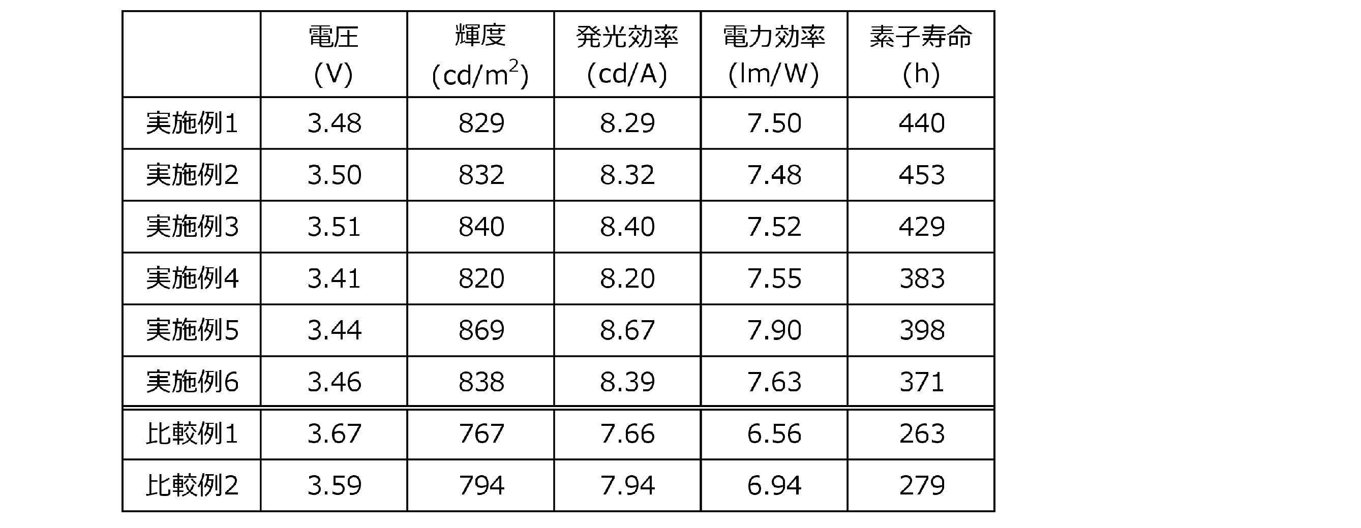
- the voltage, luminance, luminous efficiency, and power efficiency shown in Table 2 are values obtained when a current with a current density of 10 mA/cm 2 is applied at room temperature in the atmosphere.
- the life of the element is measured by constant-current driving with a current at which the emission luminance at the start of light emission (initial luminance, assumed to be 100%) is 2000 cd/m 2 , and the emission luminance is 1900 cd/m 2 (95% of the initial luminance). equivalent to: 95% attenuation).
Landscapes
- Physics & Mathematics (AREA)
- Chemical & Material Sciences (AREA)
- Engineering & Computer Science (AREA)
- Materials Engineering (AREA)
- Spectroscopy & Molecular Physics (AREA)
- Optics & Photonics (AREA)
- Organic Chemistry (AREA)
- Electroluminescent Light Sources (AREA)
Abstract
Description
前記第二正孔輸送層に下記一般式(1)または一般式(2)で表されるアミン化合物を含み、
前記第一正孔輸送層の移動度μ1および前記第二正孔輸送層の移動度μ2が、下記式(A)および式(B)を同時に満たす有機エレクトロルミネッセンス素子。
μ2>1.0×10⁻³cm2/Vs (A)
μ2/μ1>1.5 (B)

Ar1は、置換もしくは無置換の芳香族炭化水素基または置換もしくは無置換の縮合多環芳香族基を表す。

R1およびR2は、相互に同一でも異なってもよく、水素原子、重水素原子、フッ素原子、塩素原子、シアノ基、ニトロ基、置換基を有してもよい炭素原子数1~6の直鎖状もしくは分岐状のアルキル基、置換基を有してもよい炭素原子数5~10のシクロアルキル基、置換基を有してもよい炭素原子数2~6の直鎖状もしくは分岐状のアルケニル基、置換基を有してもよい炭素原子数1~6の直鎖状もしくは分岐状のアルキルオキシ基、置換基を有してもよい炭素原子数5~10のシクロアルキルオキシ基、置換もしくは無置換の芳香族炭化水素基、置換もしくは無置換の縮合多環芳香族基または置換もしくは無置換のアリールオキシ基を表す。
R1およびR2は、単結合、置換もしくは無置換のメチレン基、酸素原子または硫黄原子を介して互いに結合して環を形成してもよい。

R3は、複数存在する場合は相互に同一でも異なってもよく、水素原子、置換もしくは無置換の芳香族炭化水素基または置換もしくは無置換の縮合多環芳香族基を表し、
nは、1から5までの整数を表す。
また、R1およびR2の一方が置換基を有してもよいメチル基であり、他方がフェニル基であり、これらが単結合を介して互いに結合して五員環を形成していることも好ましい。
μ=L/(tE) (C)
μは移動度(cm2/Vs)を表し、Lは薄膜の膜厚(cm)、tは陰極までの到達時間(s)、Eは電界(V/cm)を示す。本発明における移動度は電界強度250,000(V/cm)における数値である。
実施例および比較例で使用した化合物の移動度測定を以下のようにして行った。
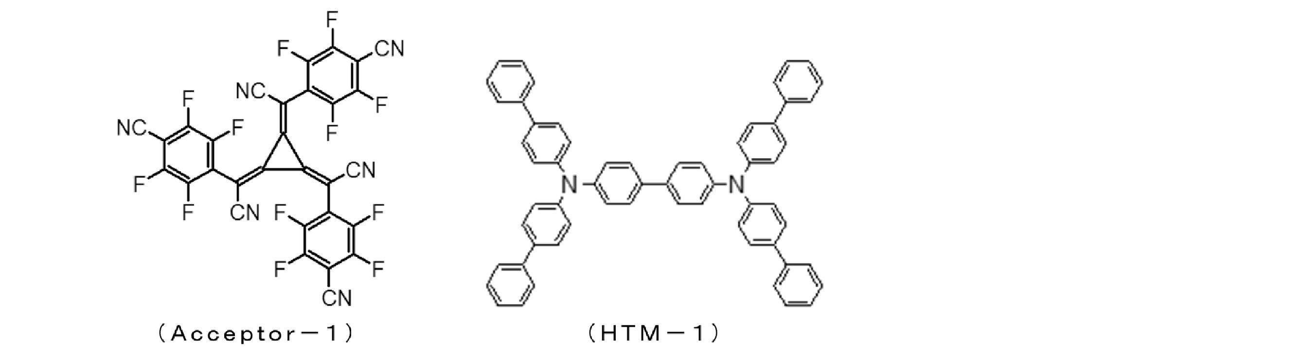
膜厚50nmのITOが製膜されたBottom基板に、第二正孔輸送層の構成材料として使用した下記化合物(1-10)、(2-3)、(2-10)をそれぞれ4μmの厚さで蒸着し、その上に陰極としてアルミニウムを膜厚100nmとなるように形成して素子を作製し、高感度キャリア移動度測定装置(住友重機械工業株式会社製、TOF-401)を用いて移動度を測定した。また、第一正孔輸送層の構成材料として使用した下記化合物(HTM-1)および(HTM-2)についても測定した。さらに、比較のために、下記化合物(HTM-3)についても測定し、結果を以下にまとめて示した。
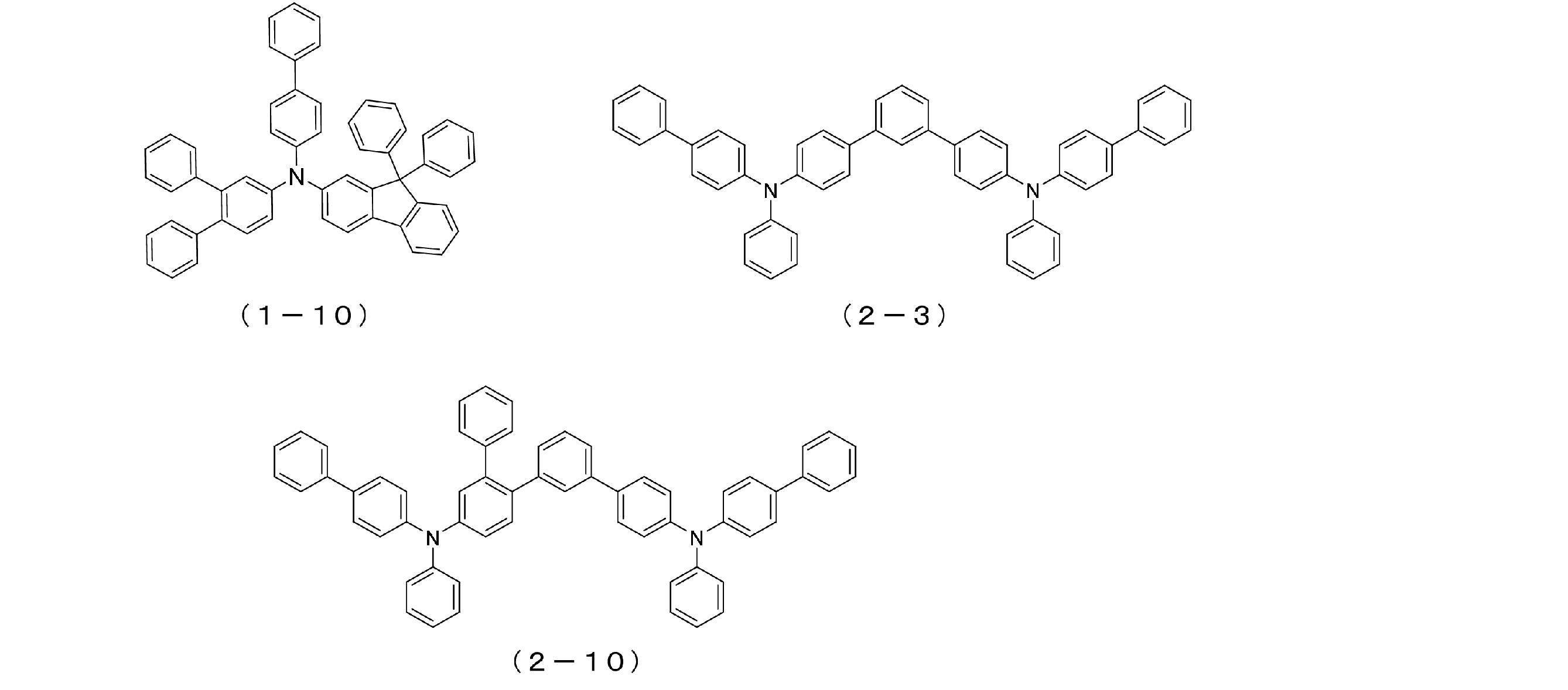

化合物(1-10) :2.63×10⁻³
化合物(2-3) :5.61×10⁻³
化合物(2-10) :3.70×10⁻³
化合物(HTM-1) :8.41×10⁻⁴
化合物(HTM-2) :5.75×10⁻⁴
化合物(HTM-3) :8.06×10⁻⁴
前記化合物を使用して有機EL素子を作製し、特性を評価した。
有機EL素子は、図3に示すように、ガラス基板1上に透明陽極2として反射ITO電極をあらかじめ形成したものの上に、正孔注入層3、第一正孔輸送層4、第二正孔輸送層5、発光層6、電子輸送層7、電子注入層8、陰極9、キャッピング層10の順に蒸着して作製した。
この正孔注入層3の上に、第一正孔輸送層4として化合物(HTM-1)を膜厚140nmとなるように形成した。
この第一正孔輸送層4の上に、第二正孔輸送層5として前記化合物(1-10)を膜厚5nmになるように形成した。
この第二正孔輸送層5の上に、発光層6として下記構造の化合物(EMD-1)と下記構造式の化合物(EMH-1)を、蒸着速度比が化合物(EMD-1):(EMH-1)=5:95となる蒸着速度で二元蒸着を行い、膜厚20nmとなるように形成した。
この発光層6の上に、電子輸送層7として下記構造式の化合物(ETM-1)と下記構造式の化合物(ETM-2)を、蒸着速度比が化合物(ETM-1):(ETM-2)=50:50となる蒸着速度で二元蒸着を行い、膜厚30nmとなるように形成した。
この電子輸送層7の上に、電子注入層8としてフッ化リチウムを膜厚1nmとなるように形成した。
この電子注入層8の上に、陰極9としてマグネシウム銀合金を膜厚12nmとなるように形成した。
最後に、キャッピング層10として下記構造式の化合物(CPL-1)を膜厚60nmとなるように形成した。
作製した有機EL素子について、前記「移動度測定」の値に基づく第二正孔輸送層の移動度(μ2)および第一正孔輸送層の移動度(μ1)、ならびに第二正孔輸送層の移動度と第一正孔輸送層の移動度の比(μ2/μ1)を計算した結果を表1にまとめて示す。また、大気中、常温で直流電圧を印加した発光特性の測定結果を表2にまとめて示す。


実施例1において、第二正孔輸送層5の材料として化合物(1-10)に代えて化合物(2-3)を用いた以外は、同様の条件で有機EL素子を作製した。作製した有機EL素子について、第二正孔輸送層の化合物(2-3)と第一正孔輸送層の化合物(HTM-1)の移動度の比(μ2/μ1)を表1にまとめて示す。また、大気中、常温で直流電圧を印加した発光特性の測定結果を表2にまとめて示す。
実施例1において、第二正孔輸送層5の材料として化合物(1-10)に代えて化合物(2-10)を用いた以外は、同様の条件で有機EL素子を作製した。作製した有機EL素子について、第二正孔輸送層の化合物(2-10)と第一正孔輸送層の化合物(HTM-1)の移動度の比(μ2/μ1)を表1にまとめて示す。また、大気中、常温で直流電圧を印加した発光特性の測定結果を表2にまとめて示す。
実施例1において、正孔注入層3および第一正孔輸送層4の材料として化合物(HTM-1)に代えて化合物(HTM-2)を用いた以外は、同様の条件で有機EL素子を作製した。作製した有機EL素子について、第二正孔輸送層の化合物(1-10)と第一正孔輸送層の化合物(HTM-2)の移動度の比(μ2/μ1)を表1にまとめて示す。また、大気中、常温で直流電圧を印加した発光特性の測定結果を表2にまとめて示す。
実施例2において、正孔注入層3および第一正孔輸送層4の材料として化合物(HTM-1)に代えて化合物(HTM-2)を用いた以外は、同様の条件で有機EL素子を作製した。作製した有機EL素子について、第二正孔輸送層の化合物(2-3)と第一正孔輸送層の化合物(HTM-2)の移動度の比(μ2/μ1)を表1にまとめて示す。また、大気中、常温で直流電圧を印加した発光特性の測定結果を表2にまとめて示す。
実施例3において、正孔注入層3および第一正孔輸送層4の材料として化合物(HTM-1)に代えて化合物(HTM-2)を用いた以外は、同様の条件で有機EL素子を作製した。作製した有機EL素子について、第二正孔輸送層の化合物(2-10)と第一正孔輸送層の化合物(HTM-2)の移動度の比(μ2/μ1)を表1にまとめて示す。また、大気中、常温で直流電圧を印加した発光特性の測定結果を表2にまとめて示す。
比較のために、実施例1において、第二正孔輸送層5の材料として化合物(1-10)に代えて化合物(HTM-3)を用いた以外は、同様の条件で有機EL素子を作製した。作製した有機EL素子について、第二正孔輸送層の化合物(HTM-3)と第一正孔輸送層の化合物(HTM-1)の移動度の比(μ2/μ1)を表1にまとめて示す。また、大気中、常温で直流電圧を印加した発光特性の測定結果を表2にまとめて示す。
比較のために、実施例4において、第二正孔輸送層5の材料として化合物(1-10)に代えて化合物(HTM-3)を用いた以外は、同様の条件で有機EL素子を作製した。作製した有機EL素子について、第二正孔輸送層の化合物(HTM-3)と第一正孔輸送層の化合物(HTM-2)の移動度の比(μ2/μ1)を表1にまとめて示す。また、大気中、常温で直流電圧を印加した発光特性の測定結果を表2にまとめて示す。

2 透明陽極
3 正孔注入層
4 第一正孔輸送層
5 第二正孔輸送層
6 発光層
7 電子輸送層
8 電子注入層
9 陰極
10 キャッピング層
Claims (6)
- 少なくとも陽極、第一正孔輸送層、第二正孔輸送層、発光層、電子輸送層および陰極をこの順に有する有機エレクトロルミネッセンス素子において、
前記第二正孔輸送層に下記一般式(1)または一般式(2)で表されるアミン化合物を含み、
前記第一正孔輸送層の移動度μ1および前記第二正孔輸送層の移動度μ2が、下記式(A)および式(B)を同時に満たす有機エレクトロルミネッセンス素子。
μ2>1.0×10⁻³cm2/Vs (A)
μ2/μ1>1.5 (B)

Ar1は、置換もしくは無置換の芳香族炭化水素基または置換もしくは無置換の縮合多環芳香族基を表す。

R1およびR2は、相互に同一でも異なってもよく、水素原子、重水素原子、フッ素原子、塩素原子、シアノ基、ニトロ基、置換基を有してもよい炭素原子数1~6の直鎖状もしくは分岐状のアルキル基、置換基を有してもよい炭素原子数5~10のシクロアルキル基、置換基を有してもよい炭素原子数2~6の直鎖状もしくは分岐状のアルケニル基、置換基を有してもよい炭素原子数1~6の直鎖状もしくは分岐状のアルキルオキシ基、置換基を有してもよい炭素原子数5~10のシクロアルキルオキシ基、置換もしくは無置換の芳香族炭化水素基、置換もしくは無置換の縮合多環芳香族基または置換もしくは無置換のアリールオキシ基を表す。
R1およびR2は、単結合、置換もしくは無置換のメチレン基、酸素原子または硫黄原子を介して互いに結合して環を形成してもよい。

R3は、複数存在する場合は相互に同一でも異なってもよく、水素原子、置換もしくは無置換の芳香族炭化水素基または置換もしくは無置換の縮合多環芳香族基を表し、
nは、1から5までの整数を表す。 - 前記一般式(1-1)で示される1価基において、R1およびR2が、相互に同一でも異なってもよく、水素原子、置換もしくは無置換の炭素数6~30の芳香族炭化水素基または置換もしくは無置換の炭素数6~30の縮合多環芳香族基である、請求項1に記載の有機エレクトロルミネッセンス素子。
- 前記一般式(1)および一般式(2)で表されるアミン化合物において、Ar1、Ar2、Ar3、Ar4およびAr5が、相互に同一でも異なっていてもよく、置換もしくは無置換の炭素数6~30の芳香族炭化水素基または置換もしくは無置換の炭素数6~30の縮合多環芳香族基である、請求項1に記載の有機エレクトロルミネッセンス素子。
- 前記第一正孔輸送層の移動度μ1が1.5×10⁻³cm2/Vs以下である、請求項1に記載の有機エレクトロルミネッセンス素子。
- 前記第二正孔輸送層の移動度μ2が2.0×10⁻³cm2/Vs以上である、請求項1に記載の有機エレクトロルミネッセンス素子。
- 前記第一正孔輸送層の膜厚が30nm超200nm未満であり、かつ前記第二正孔輸送層の膜厚が3nm超20nm未満である、請求項1~5のいずれか一項に記載の有機エレクトロルミネッセンス素子。
Priority Applications (5)
| Application Number | Priority Date | Filing Date | Title |
|---|---|---|---|
| US18/579,226 US20240349597A1 (en) | 2021-09-07 | 2022-09-05 | Organic electroluminescent element |
| CN202280050330.4A CN117730636A (zh) | 2021-09-07 | 2022-09-05 | 有机电致发光元件 |
| JP2023546934A JPWO2023038006A1 (ja) | 2021-09-07 | 2022-09-05 | |
| KR1020247000727A KR20240052742A (ko) | 2021-09-07 | 2022-09-05 | 유기 일렉트로루미네선스 소자 |
| EP22867328.1A EP4401529A4 (en) | 2021-09-07 | 2022-09-05 | ORGANIC ELECTROLUMINESCENT ELEMENT |
Applications Claiming Priority (2)
| Application Number | Priority Date | Filing Date | Title |
|---|---|---|---|
| JP2021-145744 | 2021-09-07 | ||
| JP2021145744 | 2021-09-07 |
Publications (1)
| Publication Number | Publication Date |
|---|---|
| WO2023038006A1 true WO2023038006A1 (ja) | 2023-03-16 |
Family
ID=85507620
Family Applications (1)
| Application Number | Title | Priority Date | Filing Date |
|---|---|---|---|
| PCT/JP2022/033264 Ceased WO2023038006A1 (ja) | 2021-09-07 | 2022-09-05 | 有機エレクトロルミネッセンス素子 |
Country Status (7)
| Country | Link |
|---|---|
| US (1) | US20240349597A1 (ja) |
| EP (1) | EP4401529A4 (ja) |
| JP (1) | JPWO2023038006A1 (ja) |
| KR (1) | KR20240052742A (ja) |
| CN (1) | CN117730636A (ja) |
| TW (1) | TW202323497A (ja) |
| WO (1) | WO2023038006A1 (ja) |
Citations (12)
| Publication number | Priority date | Publication date | Assignee | Title |
|---|---|---|---|---|
| US5639914A (en) | 1993-11-01 | 1997-06-17 | Hodogaya Chemical Co., Ltd. | Tetraaryl benzidines |
| US5792557A (en) | 1994-02-08 | 1998-08-11 | Tdk Corporation | Organic EL element |
| US8021764B2 (en) | 2004-11-29 | 2011-09-20 | Samsung Mobile Display Co., Ltd. | Phenylcarbazole-based compound and organic electroluminescent device employing the same |
| US8394510B2 (en) | 2006-11-24 | 2013-03-12 | Idemitsu Kosan Co., Ltd. | Aromatic amine derivative and organic electroluminescence device using the same |
| US20130313535A1 (en) * | 2012-05-22 | 2013-11-28 | Lg Display Co., Ltd. | Organic Light Emitting Device and Method of Fabricating the Same |
| WO2014009310A1 (en) | 2012-07-09 | 2014-01-16 | Novaled Ag | Doped organic semiconductive matrix material |
| US20150115231A1 (en) * | 2013-10-29 | 2015-04-30 | Samsung Display Co., Ltd. | Organic light-emitting device |
| WO2016006629A1 (ja) * | 2014-07-09 | 2016-01-14 | 保土谷化学工業株式会社 | 有機エレクトロルミネッセンス素子 |
| US20160118591A1 (en) | 2013-07-12 | 2016-04-28 | Hodogaya Chemical Co., Ltd. | Organic electroluminescent device |
| WO2018168991A1 (ja) * | 2017-03-15 | 2018-09-20 | 保土谷化学工業株式会社 | 有機エレクトロルミネッセンス素子 |
| US20190006596A1 (en) | 2016-01-14 | 2019-01-03 | Hodogaya Chemical Co., Ltd. | Organic electroluminescent device |
| KR20210106037A (ko) * | 2020-02-19 | 2021-08-30 | 삼성디스플레이 주식회사 | 표시 패널 및 이를 포함하는 표시 장치 |
Family Cites Families (3)
| Publication number | Priority date | Publication date | Assignee | Title |
|---|---|---|---|---|
| CN107210382B (zh) * | 2015-02-03 | 2020-01-10 | 保土谷化学工业株式会社 | 有机电致发光器件 |
| US11594683B2 (en) * | 2015-10-29 | 2023-02-28 | Hodogaya Chemical Co., Ltd. | Organic electroluminescent device |
| WO2019059334A1 (ja) * | 2017-09-25 | 2019-03-28 | 保土谷化学工業株式会社 | 有機エレクトロルミネッセンス素子 |
-
2022
- 2022-09-05 WO PCT/JP2022/033264 patent/WO2023038006A1/ja not_active Ceased
- 2022-09-05 US US18/579,226 patent/US20240349597A1/en active Pending
- 2022-09-05 JP JP2023546934A patent/JPWO2023038006A1/ja active Pending
- 2022-09-05 KR KR1020247000727A patent/KR20240052742A/ko active Pending
- 2022-09-05 CN CN202280050330.4A patent/CN117730636A/zh active Pending
- 2022-09-05 EP EP22867328.1A patent/EP4401529A4/en not_active Withdrawn
- 2022-09-06 TW TW111133671A patent/TW202323497A/zh unknown
Patent Citations (13)
| Publication number | Priority date | Publication date | Assignee | Title |
|---|---|---|---|---|
| US5639914A (en) | 1993-11-01 | 1997-06-17 | Hodogaya Chemical Co., Ltd. | Tetraaryl benzidines |
| US5792557A (en) | 1994-02-08 | 1998-08-11 | Tdk Corporation | Organic EL element |
| US8021764B2 (en) | 2004-11-29 | 2011-09-20 | Samsung Mobile Display Co., Ltd. | Phenylcarbazole-based compound and organic electroluminescent device employing the same |
| US8394510B2 (en) | 2006-11-24 | 2013-03-12 | Idemitsu Kosan Co., Ltd. | Aromatic amine derivative and organic electroluminescence device using the same |
| US20130313535A1 (en) * | 2012-05-22 | 2013-11-28 | Lg Display Co., Ltd. | Organic Light Emitting Device and Method of Fabricating the Same |
| WO2014009310A1 (en) | 2012-07-09 | 2014-01-16 | Novaled Ag | Doped organic semiconductive matrix material |
| US20160118591A1 (en) | 2013-07-12 | 2016-04-28 | Hodogaya Chemical Co., Ltd. | Organic electroluminescent device |
| US20150115231A1 (en) * | 2013-10-29 | 2015-04-30 | Samsung Display Co., Ltd. | Organic light-emitting device |
| WO2016006629A1 (ja) * | 2014-07-09 | 2016-01-14 | 保土谷化学工業株式会社 | 有機エレクトロルミネッセンス素子 |
| US20170179398A1 (en) | 2014-07-09 | 2017-06-22 | Hodogaya Chemical Co., Ltd. | Organic electroluminescent device |
| US20190006596A1 (en) | 2016-01-14 | 2019-01-03 | Hodogaya Chemical Co., Ltd. | Organic electroluminescent device |
| WO2018168991A1 (ja) * | 2017-03-15 | 2018-09-20 | 保土谷化学工業株式会社 | 有機エレクトロルミネッセンス素子 |
| KR20210106037A (ko) * | 2020-02-19 | 2021-08-30 | 삼성디스플레이 주식회사 | 표시 패널 및 이를 포함하는 표시 장치 |
Non-Patent Citations (4)
| Title |
|---|
| APPL. PHYS. LET., vol. 98, 2011, pages 083302 |
| PROCEEDINGS OF THE 3RD MEETING OF THE JAPAN OLED FORUM, 2006, pages 13 - 14 |
| PROCEEDINGS OF THE 9TH MEETING OF THE JAPAN SOCIETY OF APPLIED PHYSICS, 2001, pages 55 - 61 |
| See also references of EP4401529A4 |
Also Published As
| Publication number | Publication date |
|---|---|
| KR20240052742A (ko) | 2024-04-23 |
| US20240349597A1 (en) | 2024-10-17 |
| JPWO2023038006A1 (ja) | 2023-03-16 |
| TW202323497A (zh) | 2023-06-16 |
| EP4401529A1 (en) | 2024-07-17 |
| EP4401529A4 (en) | 2025-07-02 |
| CN117730636A (zh) | 2024-03-19 |
Similar Documents
| Publication | Publication Date | Title |
|---|---|---|
| JP6581225B2 (ja) | 有機エレクトロルミネッセンス素子 | |
| EP3291323B1 (en) | Organic electroluminescent element | |
| JP5807011B2 (ja) | カルバゾール環構造を有する化合物および有機エレクトロルミネッセンス素子 | |
| KR102813012B1 (ko) | 트리아릴아민 구조를 갖는 화합물 및 유기 일렉트로 루미네선스 소자 | |
| WO2011048822A1 (ja) | 有機エレクトロルミネッセンス素子 | |
| JP5977227B2 (ja) | 有機エレクトロルミネッセンス素子 | |
| CN102576813A (zh) | 有机电致发光器件 | |
| US11925107B2 (en) | Organic electroluminescent device | |
| JPWO2017033927A1 (ja) | 有機エレクトロルミネッセンス素子 | |
| KR102785437B1 (ko) | 유기 일렉트로루미네선스 소자 | |
| JPWO2019026728A1 (ja) | ベンゾアゾール環構造を有する化合物を含有する有機エレクトロルミネッセンス素子 | |
| EP4112613A1 (en) | Arylamine compound and electronic apparatus using same | |
| KR102747127B1 (ko) | 유기 일렉트로루미네선스 소자 | |
| US20230422536A1 (en) | Arylamine compound, organic electroluminescent element, and electronic device | |
| JP2023022389A (ja) | スピロビフルオレン化合物および有機エレクトロルミネッセンス素子 | |
| US20240349597A1 (en) | Organic electroluminescent element | |
| JP7179734B2 (ja) | インデノベンゾアゾール環構造を有する化合物および有機エレクトロルミネッセンス素子 | |
| JP2019034904A (ja) | 芳香族炭化水素基と2つのフタルイミド基を有する化合物および有機エレクトロルミネッセンス素子 | |
| JP2025178181A (ja) | アリールアミン化合物、有機エレクトロルミネッセンス素子、および電子機器 | |
| KR20230127061A (ko) | 아릴아민 화합물, 유기 일렉트로루미네선스 소자, 및 전자 기기 |
Legal Events
| Date | Code | Title | Description |
|---|---|---|---|
| WWE | Wipo information: entry into national phase |
Ref document number: 2023546934 Country of ref document: JP |
|
| WWE | Wipo information: entry into national phase |
Ref document number: 202280050330.4 Country of ref document: CN |
|
| WWE | Wipo information: entry into national phase |
Ref document number: 2022867328 Country of ref document: EP |
|
| NENP | Non-entry into the national phase |
Ref country code: DE |
|
| ENP | Entry into the national phase |
Ref document number: 2022867328 Country of ref document: EP Effective date: 20240408 |
|
| WWW | Wipo information: withdrawn in national office |
Ref document number: 2022867328 Country of ref document: EP |