WO2023042339A1 - 光学測定システムおよび光学測定方法 - Google Patents
光学測定システムおよび光学測定方法 Download PDFInfo
- Publication number
- WO2023042339A1 WO2023042339A1 PCT/JP2021/034111 JP2021034111W WO2023042339A1 WO 2023042339 A1 WO2023042339 A1 WO 2023042339A1 JP 2021034111 W JP2021034111 W JP 2021034111W WO 2023042339 A1 WO2023042339 A1 WO 2023042339A1
- Authority
- WO
- WIPO (PCT)
- Prior art keywords
- light
- sample
- hologram
- optical system
- optical
- Prior art date
- Legal status (The legal status is an assumption and is not a legal conclusion. Google has not performed a legal analysis and makes no representation as to the accuracy of the status listed.)
- Ceased
Links
Images






Classifications
-
- G—PHYSICS
- G01—MEASURING; TESTING
- G01N—INVESTIGATING OR ANALYSING MATERIALS BY DETERMINING THEIR CHEMICAL OR PHYSICAL PROPERTIES
- G01N21/00—Investigating or analysing materials by the use of optical means, i.e. using sub-millimetre waves, infrared, visible or ultraviolet light
- G01N21/84—Systems specially adapted for particular applications
- G01N21/88—Investigating the presence of flaws or contamination
- G01N21/95—Investigating the presence of flaws or contamination characterised by the material or shape of the object to be examined
- G01N21/9501—Semiconductor wafers
- G01N21/9505—Wafer internal defects, e.g. microcracks
-
- G—PHYSICS
- G01—MEASURING; TESTING
- G01N—INVESTIGATING OR ANALYSING MATERIALS BY DETERMINING THEIR CHEMICAL OR PHYSICAL PROPERTIES
- G01N21/00—Investigating or analysing materials by the use of optical means, i.e. using sub-millimetre waves, infrared, visible or ultraviolet light
- G01N21/17—Systems in which incident light is modified in accordance with the properties of the material investigated
- G01N21/41—Refractivity; Phase-affecting properties, e.g. optical path length
- G01N21/45—Refractivity; Phase-affecting properties, e.g. optical path length using interferometric methods; using Schlieren methods
-
- G—PHYSICS
- G01—MEASURING; TESTING
- G01B—MEASURING LENGTH, THICKNESS OR SIMILAR LINEAR DIMENSIONS; MEASURING ANGLES; MEASURING AREAS; MEASURING IRREGULARITIES OF SURFACES OR CONTOURS
- G01B11/00—Measuring arrangements characterised by the use of optical techniques
- G01B11/24—Measuring arrangements characterised by the use of optical techniques for measuring contours or curvatures
-
- G—PHYSICS
- G01—MEASURING; TESTING
- G01B—MEASURING LENGTH, THICKNESS OR SIMILAR LINEAR DIMENSIONS; MEASURING ANGLES; MEASURING AREAS; MEASURING IRREGULARITIES OF SURFACES OR CONTOURS
- G01B11/00—Measuring arrangements characterised by the use of optical techniques
- G01B11/24—Measuring arrangements characterised by the use of optical techniques for measuring contours or curvatures
- G01B11/2441—Measuring arrangements characterised by the use of optical techniques for measuring contours or curvatures using interferometry
-
- G—PHYSICS
- G01—MEASURING; TESTING
- G01B—MEASURING LENGTH, THICKNESS OR SIMILAR LINEAR DIMENSIONS; MEASURING ANGLES; MEASURING AREAS; MEASURING IRREGULARITIES OF SURFACES OR CONTOURS
- G01B9/00—Measuring instruments characterised by the use of optical techniques
- G01B9/02—Interferometers
- G01B9/02041—Interferometers characterised by particular imaging or detection techniques
- G01B9/02047—Interferometers characterised by particular imaging or detection techniques using digital holographic imaging, e.g. lensless phase imaging without hologram in the reference path
-
- G—PHYSICS
- G01—MEASURING; TESTING
- G01B—MEASURING LENGTH, THICKNESS OR SIMILAR LINEAR DIMENSIONS; MEASURING ANGLES; MEASURING AREAS; MEASURING IRREGULARITIES OF SURFACES OR CONTOURS
- G01B9/00—Measuring instruments characterised by the use of optical techniques
- G01B9/02—Interferometers
- G01B9/021—Interferometers using holographic techniques
-
- G—PHYSICS
- G01—MEASURING; TESTING
- G01N—INVESTIGATING OR ANALYSING MATERIALS BY DETERMINING THEIR CHEMICAL OR PHYSICAL PROPERTIES
- G01N21/00—Investigating or analysing materials by the use of optical means, i.e. using sub-millimetre waves, infrared, visible or ultraviolet light
- G01N21/17—Systems in which incident light is modified in accordance with the properties of the material investigated
- G01N21/25—Colour; Spectral properties, i.e. comparison of effect of material on the light at two or more different wavelengths or wavelength bands
- G01N21/31—Investigating relative effect of material at wavelengths characteristic of specific elements or molecules, e.g. atomic absorption spectrometry
- G01N21/35—Investigating relative effect of material at wavelengths characteristic of specific elements or molecules, e.g. atomic absorption spectrometry using infrared light
- G01N21/3563—Investigating relative effect of material at wavelengths characteristic of specific elements or molecules, e.g. atomic absorption spectrometry using infrared light for analysing solids; Preparation of samples therefor
-
- G—PHYSICS
- G01—MEASURING; TESTING
- G01N—INVESTIGATING OR ANALYSING MATERIALS BY DETERMINING THEIR CHEMICAL OR PHYSICAL PROPERTIES
- G01N21/00—Investigating or analysing materials by the use of optical means, i.e. using sub-millimetre waves, infrared, visible or ultraviolet light
- G01N21/17—Systems in which incident light is modified in accordance with the properties of the material investigated
- G01N21/25—Colour; Spectral properties, i.e. comparison of effect of material on the light at two or more different wavelengths or wavelength bands
- G01N21/31—Investigating relative effect of material at wavelengths characteristic of specific elements or molecules, e.g. atomic absorption spectrometry
- G01N21/35—Investigating relative effect of material at wavelengths characteristic of specific elements or molecules, e.g. atomic absorption spectrometry using infrared light
- G01N21/359—Investigating relative effect of material at wavelengths characteristic of specific elements or molecules, e.g. atomic absorption spectrometry using infrared light using near infrared light
-
- G—PHYSICS
- G01—MEASURING; TESTING
- G01N—INVESTIGATING OR ANALYSING MATERIALS BY DETERMINING THEIR CHEMICAL OR PHYSICAL PROPERTIES
- G01N21/00—Investigating or analysing materials by the use of optical means, i.e. using sub-millimetre waves, infrared, visible or ultraviolet light
- G01N21/17—Systems in which incident light is modified in accordance with the properties of the material investigated
- G01N21/41—Refractivity; Phase-affecting properties, e.g. optical path length
- G01N21/45—Refractivity; Phase-affecting properties, e.g. optical path length using interferometric methods; using Schlieren methods
- G01N21/453—Holographic interferometry
-
- G—PHYSICS
- G01—MEASURING; TESTING
- G01N—INVESTIGATING OR ANALYSING MATERIALS BY DETERMINING THEIR CHEMICAL OR PHYSICAL PROPERTIES
- G01N21/00—Investigating or analysing materials by the use of optical means, i.e. using sub-millimetre waves, infrared, visible or ultraviolet light
- G01N21/84—Systems specially adapted for particular applications
- G01N21/88—Investigating the presence of flaws or contamination
-
- G—PHYSICS
- G01—MEASURING; TESTING
- G01N—INVESTIGATING OR ANALYSING MATERIALS BY DETERMINING THEIR CHEMICAL OR PHYSICAL PROPERTIES
- G01N21/00—Investigating or analysing materials by the use of optical means, i.e. using sub-millimetre waves, infrared, visible or ultraviolet light
- G01N21/84—Systems specially adapted for particular applications
- G01N21/88—Investigating the presence of flaws or contamination
- G01N21/8806—Specially adapted optical and illumination features
-
- G—PHYSICS
- G03—PHOTOGRAPHY; CINEMATOGRAPHY; ANALOGOUS TECHNIQUES USING WAVES OTHER THAN OPTICAL WAVES; ELECTROGRAPHY; HOLOGRAPHY
- G03H—HOLOGRAPHIC PROCESSES OR APPARATUS
- G03H1/00—Holographic processes or apparatus using light, infrared or ultraviolet waves for obtaining holograms or for obtaining an image from them; Details peculiar thereto
- G03H1/0005—Adaptation of holography to specific applications
-
- G—PHYSICS
- G03—PHOTOGRAPHY; CINEMATOGRAPHY; ANALOGOUS TECHNIQUES USING WAVES OTHER THAN OPTICAL WAVES; ELECTROGRAPHY; HOLOGRAPHY
- G03H—HOLOGRAPHIC PROCESSES OR APPARATUS
- G03H1/00—Holographic processes or apparatus using light, infrared or ultraviolet waves for obtaining holograms or for obtaining an image from them; Details peculiar thereto
- G03H1/04—Processes or apparatus for producing holograms
- G03H1/0443—Digital holography, i.e. recording holograms with digital recording means
-
- G—PHYSICS
- G03—PHOTOGRAPHY; CINEMATOGRAPHY; ANALOGOUS TECHNIQUES USING WAVES OTHER THAN OPTICAL WAVES; ELECTROGRAPHY; HOLOGRAPHY
- G03H—HOLOGRAPHIC PROCESSES OR APPARATUS
- G03H1/00—Holographic processes or apparatus using light, infrared or ultraviolet waves for obtaining holograms or for obtaining an image from them; Details peculiar thereto
- G03H1/04—Processes or apparatus for producing holograms
- G03H1/0465—Particular recording light; Beam shape or geometry
-
- G—PHYSICS
- G03—PHOTOGRAPHY; CINEMATOGRAPHY; ANALOGOUS TECHNIQUES USING WAVES OTHER THAN OPTICAL WAVES; ELECTROGRAPHY; HOLOGRAPHY
- G03H—HOLOGRAPHIC PROCESSES OR APPARATUS
- G03H1/00—Holographic processes or apparatus using light, infrared or ultraviolet waves for obtaining holograms or for obtaining an image from them; Details peculiar thereto
- G03H1/04—Processes or apparatus for producing holograms
- G03H1/08—Synthesising holograms, i.e. holograms synthesized from objects or objects from holograms
-
- G—PHYSICS
- G03—PHOTOGRAPHY; CINEMATOGRAPHY; ANALOGOUS TECHNIQUES USING WAVES OTHER THAN OPTICAL WAVES; ELECTROGRAPHY; HOLOGRAPHY
- G03H—HOLOGRAPHIC PROCESSES OR APPARATUS
- G03H1/00—Holographic processes or apparatus using light, infrared or ultraviolet waves for obtaining holograms or for obtaining an image from them; Details peculiar thereto
- G03H1/04—Processes or apparatus for producing holograms
- G03H1/08—Synthesising holograms, i.e. holograms synthesized from objects or objects from holograms
- G03H1/0866—Digital holographic imaging, i.e. synthesizing holobjects from holograms
-
- G—PHYSICS
- G03—PHOTOGRAPHY; CINEMATOGRAPHY; ANALOGOUS TECHNIQUES USING WAVES OTHER THAN OPTICAL WAVES; ELECTROGRAPHY; HOLOGRAPHY
- G03H—HOLOGRAPHIC PROCESSES OR APPARATUS
- G03H1/00—Holographic processes or apparatus using light, infrared or ultraviolet waves for obtaining holograms or for obtaining an image from them; Details peculiar thereto
- G03H1/0005—Adaptation of holography to specific applications
- G03H2001/0033—Adaptation of holography to specific applications in hologrammetry for measuring or analysing
-
- G—PHYSICS
- G03—PHOTOGRAPHY; CINEMATOGRAPHY; ANALOGOUS TECHNIQUES USING WAVES OTHER THAN OPTICAL WAVES; ELECTROGRAPHY; HOLOGRAPHY
- G03H—HOLOGRAPHIC PROCESSES OR APPARATUS
- G03H1/00—Holographic processes or apparatus using light, infrared or ultraviolet waves for obtaining holograms or for obtaining an image from them; Details peculiar thereto
- G03H1/0005—Adaptation of holography to specific applications
- G03H2001/0033—Adaptation of holography to specific applications in hologrammetry for measuring or analysing
- G03H2001/0038—Adaptation of holography to specific applications in hologrammetry for measuring or analysing analogue or digital holobjects
-
- G—PHYSICS
- G03—PHOTOGRAPHY; CINEMATOGRAPHY; ANALOGOUS TECHNIQUES USING WAVES OTHER THAN OPTICAL WAVES; ELECTROGRAPHY; HOLOGRAPHY
- G03H—HOLOGRAPHIC PROCESSES OR APPARATUS
- G03H1/00—Holographic processes or apparatus using light, infrared or ultraviolet waves for obtaining holograms or for obtaining an image from them; Details peculiar thereto
- G03H1/0005—Adaptation of holography to specific applications
- G03H2001/005—Adaptation of holography to specific applications in microscopy, e.g. digital holographic microscope [DHM]
-
- G—PHYSICS
- G03—PHOTOGRAPHY; CINEMATOGRAPHY; ANALOGOUS TECHNIQUES USING WAVES OTHER THAN OPTICAL WAVES; ELECTROGRAPHY; HOLOGRAPHY
- G03H—HOLOGRAPHIC PROCESSES OR APPARATUS
- G03H1/00—Holographic processes or apparatus using light, infrared or ultraviolet waves for obtaining holograms or for obtaining an image from them; Details peculiar thereto
- G03H1/04—Processes or apparatus for producing holograms
- G03H1/0443—Digital holography, i.e. recording holograms with digital recording means
- G03H2001/0445—Off-axis recording arrangement
-
- G—PHYSICS
- G03—PHOTOGRAPHY; CINEMATOGRAPHY; ANALOGOUS TECHNIQUES USING WAVES OTHER THAN OPTICAL WAVES; ELECTROGRAPHY; HOLOGRAPHY
- G03H—HOLOGRAPHIC PROCESSES OR APPARATUS
- G03H1/00—Holographic processes or apparatus using light, infrared or ultraviolet waves for obtaining holograms or for obtaining an image from them; Details peculiar thereto
- G03H1/04—Processes or apparatus for producing holograms
- G03H1/0443—Digital holography, i.e. recording holograms with digital recording means
- G03H2001/0447—In-line recording arrangement
-
- G—PHYSICS
- G03—PHOTOGRAPHY; CINEMATOGRAPHY; ANALOGOUS TECHNIQUES USING WAVES OTHER THAN OPTICAL WAVES; ELECTROGRAPHY; HOLOGRAPHY
- G03H—HOLOGRAPHIC PROCESSES OR APPARATUS
- G03H1/00—Holographic processes or apparatus using light, infrared or ultraviolet waves for obtaining holograms or for obtaining an image from them; Details peculiar thereto
- G03H1/04—Processes or apparatus for producing holograms
- G03H1/0443—Digital holography, i.e. recording holograms with digital recording means
- G03H2001/045—Fourier or lensless Fourier arrangement
-
- G—PHYSICS
- G03—PHOTOGRAPHY; CINEMATOGRAPHY; ANALOGOUS TECHNIQUES USING WAVES OTHER THAN OPTICAL WAVES; ELECTROGRAPHY; HOLOGRAPHY
- G03H—HOLOGRAPHIC PROCESSES OR APPARATUS
- G03H1/00—Holographic processes or apparatus using light, infrared or ultraviolet waves for obtaining holograms or for obtaining an image from them; Details peculiar thereto
- G03H1/04—Processes or apparatus for producing holograms
- G03H1/0443—Digital holography, i.e. recording holograms with digital recording means
- G03H2001/0454—Arrangement for recovering hologram complex amplitude
- G03H2001/0456—Spatial heterodyne, i.e. filtering a Fourier transform of the off-axis record
-
- G—PHYSICS
- G03—PHOTOGRAPHY; CINEMATOGRAPHY; ANALOGOUS TECHNIQUES USING WAVES OTHER THAN OPTICAL WAVES; ELECTROGRAPHY; HOLOGRAPHY
- G03H—HOLOGRAPHIC PROCESSES OR APPARATUS
- G03H2222/00—Light sources or light beam properties
- G03H2222/40—Particular irradiation beam not otherwise provided for
- G03H2222/42—Reference beam at recording stage
-
- G—PHYSICS
- G03—PHOTOGRAPHY; CINEMATOGRAPHY; ANALOGOUS TECHNIQUES USING WAVES OTHER THAN OPTICAL WAVES; ELECTROGRAPHY; HOLOGRAPHY
- G03H—HOLOGRAPHIC PROCESSES OR APPARATUS
- G03H2222/00—Light sources or light beam properties
- G03H2222/40—Particular irradiation beam not otherwise provided for
- G03H2222/44—Beam irradiating the object at recording stage
-
- G—PHYSICS
- G03—PHOTOGRAPHY; CINEMATOGRAPHY; ANALOGOUS TECHNIQUES USING WAVES OTHER THAN OPTICAL WAVES; ELECTROGRAPHY; HOLOGRAPHY
- G03H—HOLOGRAPHIC PROCESSES OR APPARATUS
- G03H2222/00—Light sources or light beam properties
- G03H2222/50—Geometrical property of the irradiating beam
- G03H2222/52—Divergent beam
-
- G—PHYSICS
- G03—PHOTOGRAPHY; CINEMATOGRAPHY; ANALOGOUS TECHNIQUES USING WAVES OTHER THAN OPTICAL WAVES; ELECTROGRAPHY; HOLOGRAPHY
- G03H—HOLOGRAPHIC PROCESSES OR APPARATUS
- G03H2223/00—Optical components
- G03H2223/12—Amplitude mask, e.g. diaphragm, Louver filter
Definitions
- the present invention relates to an optical measurement system and an optical measurement method using digital holography.
- Patent Document 1 discloses a technique for inspecting defects inside and on the front and back surfaces of a wafer using a transmission image obtained by irradiating the wafer with infrared light. Also, there is a well-known device that implements wafer internal defect inspection using infrared light (see Non-Patent Document 1, etc.).
- Digital holography has been proposed and put into practical use as a method of measuring the shape of samples with higher accuracy.
- Digital holography is a technology that acquires the shape of the wavefront of the object light and measures the shape of the sample, etc. is.
- Patent Document 2 discloses a configuration capable of measuring the shape of a sample by adopting a reflective optical system.
- Patent Document 3 uses a cube-shaped beam combiner and discloses a configuration that can easily realize large numerical aperture recording and reflective illumination.
- Patent Document 1 The technique disclosed in JP-A-2011-033449 (Patent Document 1) described above employs a measurement method based on the difference in transmittance of infrared light, and it is difficult to detect nm-order defects.
- the wafer internal defect inspection described above also employs a measurement method based on the difference in transmittance of infrared light, and it is difficult to detect nm-order defects.
- An optical measurement system includes a first light source that produces near-infrared radiation, a silicon-based image sensor, and a beam that splits light from the first light source into first and second light beams. and an optical system including a splitter.
- the optical system is configured to record, with the image sensor, a first hologram obtained by illuminating the sample with the first light and modulating the light with the second light, which is divergent light.
- the optical system may generate the first hologram from transmitted light obtained by illuminating the sample with the first light.
- the second hologram may be recorded from transmitted light obtained by illuminating a substrate included in the sample and not to be measured with the first light.
- the optical system may generate the first hologram from reflected light obtained by illuminating the sample with the first light.
- the second hologram may be recorded from reflected light obtained by illuminating the reference reference surface with the first light.
- the optical measurement system may further include a second light source that generates visible light and a processor.
- the optical system has a first configuration for generating a first hologram from transmitted light obtained by illuminating the sample with the first light, and a first configuration for generating the first hologram from reflected light obtained by illuminating the sample with the first light. It may be changeable between a second configuration for generating a hologram.
- a processor measures the internal structure of the sample based on a first hologram recorded when the first light source and first configuration of the optical system are combined, and measures the internal structure of the sample using a second light source and a second configuration of the optical system.
- the surface shape of the sample may be measured based on the first hologram recorded when the configuration of (1) is combined.
- the optical system may be an off-axis holographic optical system.
- the optical system converts the sample into the first light so that the component corresponding to the first light and the component other than the component corresponding to the first light do not overlap in the spatial frequency domain of the hologram recorded by the image sensor.
- an optical measurement method using an optical system including a beam splitter that splits light from a first light source that generates near-infrared rays into first light and second light.
- the optical measurement method includes the steps of: recording a first hologram obtained by illuminating a sample with a first light and modulating the light with a second light that is divergent light with a silicon-based image sensor; recording, with the image sensor, a second hologram in which the first light is modulated with the second light.
- An optical measurement system includes a light source, an optical system including a beam splitter for splitting light from the light source into first light and second light, and recording a hologram generated by the optical system. a first hologram obtained by illuminating a sample with the first light and modulating the light with the second light; and a processor for calculating, based on the modulated second hologram, an amplitude-phase distribution in the sample plane, which is the plane of interest of the sample.
- the optical system includes a mechanism for changing the form of illumination with the first light.
- the processing device is configured to calculate a synthetic amplitude-phase distribution by integrating the amplitude-phase distributions calculated for each form of illumination with the first light as they are as complex numbers.
- the mechanism may change the angle of illumination of the first light.
- the mechanism may change the azimuth angle while keeping the incident angle of the first light constant.
- the optical system converts the sample into the first light so that the component corresponding to the first light and the component other than the component corresponding to the first light do not overlap in the spatial frequency domain of the hologram recorded by the image sensor.
- the optical system may include a limiter that limits the size of the area illuminated by .
- the processing device may provide a user interface screen for accepting the setting of the number of forms illuminated with the first light.
- an optical measurement method using an optical system including a beam splitter that splits light from a light source into first light and second light.
- the optical measurement method includes the step of recording, with an image sensor, a first hologram obtained by illuminating a sample with a first light and modulating the light with a second light; a step of recording a second hologram obtained by modulating light with a second light with an image sensor; a step of changing a form of illumination with the first light; a step of calculating an amplitude-phase distribution on a sample surface, which is a surface of interest of the sample, based on the hologram and the second hologram; and calculating a composite amplitude-phase distribution by accumulating complex numbers as they are.
- FIG. 1 is a schematic diagram showing a configuration example of an optical measurement system according to Embodiment 1;
- FIG. 2 is a schematic diagram showing a detailed configuration example of a measurement optical system in the optical measurement system according to Embodiment 1;
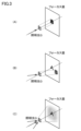
- FIG. FIG. 5 is a diagram for explaining the effect obtained by changing the form of illuminating illumination light in the optical measurement system according to the present embodiment;
- FIG. 4 is a diagram for explaining how object light and off-axis reference light are incident on a recording surface of an image sensor;
- FIG. 4 is a diagram for explaining the relationship between a sample and off-axis reference beam R in the optical measurement system according to this embodiment;
- FIG. 4 is a diagram for explaining the relationship of spatial frequency bands for off-axis holograms in the optical measurement system according to the present embodiment;
- 5 is a flow chart showing a processing procedure of a surface shape measuring method using the optical measuring system according to Embodiment 1;
- 5 is a flow chart showing a processing procedure of an internal structure measuring method using the optical measuring system according to Embodiment 1;
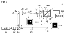
- FIG. 9 is a schematic diagram showing a configuration example of an optical measurement system according to Embodiment 2;
- 9 is a flow chart showing a processing procedure of a surface profile measuring method using the optical measuring system according to the second embodiment;
- 9 is a flow chart showing a processing procedure of an internal structure measuring method using the optical measuring system according to the second embodiment;
- FIG. 2 is a schematic diagram showing a hardware configuration example of a processing device included in the optical measurement system according to the present embodiment
- FIG. 2 is a schematic diagram showing an example functional configuration of a processing device included in the optical measurement system according to the present embodiment
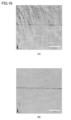
- FIG. 4 is a schematic diagram showing an example of a user interface screen provided in the optical measurement system according to the present embodiment; It is a figure which shows the example of a surface shape measurement by the optical measurement system according to this Embodiment.
- FIG. 4 is a diagram showing an example of internal structure measurement by the optical measurement system according to the present embodiment
- 1 is a schematic diagram showing an example of a composite configuration of an optical measurement system according to this embodiment;
- the optical measurement system utilizes digital holography using divergent light, such as a point light source, as reference light.
- divergent light such as a point light source
- Embodiment 1 a transmissive optical system is exemplified, and in Embodiment 2, a reflective optical system is exemplified.
- the present embodiment can include the first embodiment and the second embodiment.
- the optical measurement system according to this embodiment measures the surface shape and internal structure of a sample. Furthermore, the optical measurement system according to this embodiment can also measure the refractive index of the sample. Although any sample can be measured, for example, it can be used for surface inspection of semiconductors, measurement of thickness and refractive index distribution of film products, evaluation of surface roughness and undulation of precision processed surfaces, observation and shape evaluation of living cells, etc. can be done.
- FIG. 1 is a schematic diagram showing a configuration example of an optical measurement system 1 according to the first embodiment.
- FIG. 1A shows an optical system for recording in-line reference light
- FIG. 1B shows an optical system for recording object light.
- the optical measurement system 1 can configure the optical system shown in FIGS. 1(A) and 1(B).
- the optical system shown in FIG. 1A corresponds to an optical system for recording an off-axis hologram ILR obtained by modulating an in-line reference beam L, which serves as a reference for recording, with an off-axis reference beam R.
- FIG. 1A corresponds to an optical system for recording an off-axis hologram ILR obtained by modulating an in-line reference beam L, which serves as a reference for recording, with an off-axis reference beam R.
- the optical system shown in FIG. 1(B) modulates object light O obtained by illuminating a sample S with illumination light Q with off-axis reference light R, which is divergent light, to record an off-axis hologram IOR .
- the optical system shown in FIG. 1B generates an off-axis hologram I OR (object beam hologram: first hologram) from transmitted light obtained by illuminating the sample S with illumination light Q. .
- An illumination light profile is also acquired using the optical system shown in FIG. In this case, sample S is not placed.
- the processing device 100 measures the surface shape, internal structure, etc. of the sample S based on the off-axis hologram ILR and the off-axis hologram IOR .
- optical measurement system 1 includes a light source 10, a beam expander BE, beam splitters BS1 and BS2, mirrors M1 and M1, as an optical system for recording off-axis hologram ILR .
- M2 an objective lens MO, a pinhole P, a lens L1, a mask A1, and an image sensor D.
- the light source 10 is composed of a laser or the like, and generates coherent light.
- the wavelength band of the light generated by light source 10 may be varied according to the content of measurement (measurement of surface shape or measurement of internal structure).
- the light source 10 that generates visible light when measuring the surface shape of the sample S, the light source 10 that generates visible light may be used.
- a light source 10 that generates light having components in at least part of the wavelength range of 380 to 780 nm is used.
- a visible light source with a peak wavelength at 532 nm may be used.
- the light source 10 that emits near-infrared rays may be used.
- a light source 10 is used that generates light having components in at least part of the wavelength range of 1000 to 1200 nm.
- a near-infrared light source with a peak wavelength at 1030 nm may be used.
- the optical measurement system according to the present embodiment is configured so that the type of light source 10 can be arbitrarily changed.
- the image sensor D records a hologram generated by the optical system shown in FIGS. 1(A) and 1(B).
- a general CCD (Charge-Coupled Device) image sensor or CMOS (Complementary MOS) image sensor is used as the image sensor D.
- These image sensors are semiconductor integrated circuits consisting of electronic circuits formed on silicon substrates. That is, a silicon-based image sensor is used in the optical measurement system according to this embodiment.
- a silicon-based image sensor has photosensitivity mainly in the visible light band, and also has photosensitivity to near-infrared light in addition to visible light.
- the beam expander BE expands the cross-sectional diameter of light from the light source 10 to a predetermined size.
- the beam splitter BS1 splits the light expanded by the beam expander BE into two.
- One light split by the beam splitter BS1 corresponds to the in-line reference light L (first light), and the other light corresponds to the off-axis reference light R (second light).
- the in-line reference light L is reflected by the mirror M2 and guided to the beam splitter BS2. Furthermore, the in-line reference light L is guided to the image sensor D through the half mirror HM2 of the beam splitter BS2.
- An objective lens MO and a pinhole P are arranged between the mirror M2 and the beam splitter BS2.
- the in-line reference light L is condensed by the objective lens MO and narrowed by the pinhole P in cross-sectional diameter.
- a pinhole P corresponds to the position of the point light source of the in-line reference light L.
- FIG. An objective lens MO and a pinhole P realize a point source of in-line reference light L.
- the off-axis reference beam R is reflected by the mirror M1 and guided to the beam splitter BS2. Furthermore, the off-axis reference beam R is guided to the image sensor D by being reflected by the half mirror HM2 of the beam splitter BS2. A mask A1 and a lens L1 are arranged between the mirror M1 and the beam splitter BS2. After passing through the mask A1, the off-axis reference beam R is condensed by the lens L1.
- the mask A1 has an aperture pattern SP1 in the region through which the off-axis reference beam R passes.
- An image corresponding to the aperture pattern SP1 of the mask A1 is formed on the image sensor D.
- the size of the aperture pattern SP1 of the mask A1 is determined so that the off-axis reference light R that has passed through the mask A1 does not illuminate a range beyond the surface of the beam splitter BS2 on the image sensor D side. Determining the size of the aperture pattern SP1 of the mask A1 in this manner suppresses the generation of noise due to unnecessary interference.
- the off-axis reference beam R is adjusted so that the in-line reference beam L can be recorded as a hologram.
- the in-line reference beam L and the off-axis reference beam R are superimposed by the beam splitter BS2 placed in front of the image sensor D through the optical path as described above. That is, the image sensor D obtains an off-axis hologram ILR obtained by modulating the in-line reference light L with the off-axis reference light R, which is divergent light.
- the beam splitter BS2 is preferably configured in a cube shape so that it can be easily arranged in front of the image sensor D.
- the point source of the in-line reference beam L and the point source of the off-axis reference beam R are brought into optical proximity by the beam splitter BS2.
- optical measurement system 1 includes measurement optical system 30 instead of mirror M2, objective lens MO and pinhole P as an optical system for recording off-axis hologram IOR . include.
- the measurement optical system 30 has a mechanism for changing the form of illumination light and a mechanism for limiting the illumination range. More specifically, the measurement optical system 30 includes a movable mirror MM, lenses L2, L31, L32 and a mask A2.
- a sample S to be measured is placed between the measurement optical system 30 and the beam splitter BS2.
- the distance required by the measurement optical system 30 is longer than the distance required by the objective lens MO and the pinhole P of the optical system shown in FIG. It is arranged at a position closer to the light source 10 side.
- the light output from one side of the beam splitter BS1 is used as illumination light Q (first light) for illuminating the sample S.
- the optical measurement system has a mechanism for changing the form of illumination with the illumination light Q.
- FIG. 1B shows a movable mirror MM. More specifically, the illuminating form of the illumination light Q is changed by rotating the movable mirror MM.
- a change in the form of illuminating the illumination light Q means a change in the angle at which the illumination light Q is illuminated. Below, the angle which illuminates the illumination light Q is also called an "illumination angle.”
- the off-axis reference light R (second light) output from the other beam splitter BS1 is guided to the image sensor D through the optical path common to that in FIG. 1(A).
- the object light O obtained by illuminating the sample S with the illumination light Q (that is, the light transmitted through the sample S) is transmitted through the half mirror HM2 of the beam splitter BS2 and guided to the image sensor D.
- a lens L3, a mask A2, and a lens L2 are arranged in this order between the movable mirror MM and the beam splitter BS2.
- Illumination light Q is condensed by lens L3 and passes through mask A2.
- the illumination light Q that has passed through the mask A2 is further condensed by the lens L2 and forms an image on the sample S.
- the mask A2 corresponds to a limiting portion that limits the range of illumination of the sample S with the illumination light Q to a predetermined range.
- a mask A2 in which an opening pattern SP2 corresponding to a predetermined range is formed in the shielding member may be used.
- the illumination light Q passes through the area corresponding to the aperture pattern SP2.
- the image of the aperture pattern SP2 of the mask A2 passes through the lens L2 and forms an image on the sample S. That is, of the light illuminating the mask A2, only the light corresponding to the aperture pattern SP2 passes through the mask A2.
- the range in which the illumination light Q that has passed through the mask A2 illuminates the sample S can be limited.
- unnecessary light can be reduced and measurement accuracy can be improved.
- the illumination range may vary depending on the thickness of the sample S.
- the aperture pattern SP2 of the mask A2 is changed as necessary, or the illumination range is changed.
- the position of the lens L2 for imaging the light Q onto the sample S is changed.
- the configuration for illuminating the mask A2 with the illumination light Q is not limited to the configuration shown in FIG. 1(B), and any configuration can be adopted.
- FIG. 2 is a schematic diagram showing a detailed configuration example of the measurement optical system 30 in the optical measurement system 1 according to the first embodiment.
- the illumination light Q passes through the movable mirror MM, the lens L31, the lens L32, the mask A2, and the lens L2 in this order, and forms an image on the sample S.
- the lens L31 and the lens L32 constitute an imaging optical system 20 such as a 4f optical system.
- the illumination light Q incident on the movable mirror MM is reflected in a direction corresponding to the angle (orientation) of the movable mirror MM and enters the imaging optical system 20 .
- the illumination light Q propagates in the direction reflected by the movable mirror MM, passes through the aperture pattern SP2 of the mask A2, and forms an image on the sample S in the same shape as the aperture pattern SP2.
- FIG. 2(B) shows an example of an optical system in which the illumination light Q that illuminates the sample S is parallel light. More specifically, in the optical system shown in FIG. 2B, lenses L21 and L22 are arranged instead of the lens L2 in the optical system shown in FIG. 2A. Both the lens L21 and the lens L22 are condenser lenses, and by combining them, the illumination light Q that has passed through the mask A2 illuminates the sample S as parallel light.
- the optical systems arranged before and after the mask A2 are not limited to the optical systems shown in FIGS. 2(A) and 2(B).
- any configuration may be adopted as long as the reflected light from the movable mirror MM can be projected so as to cover the aperture pattern SP2 of the mask A2.
- any configuration may be adopted as long as the image of the aperture pattern SP2 of the mask A2 can be formed on the sample S.
- the number and types of lenses can be arbitrarily designed.
- the lenses L31 and L32 may be omitted.
- the light-receiving surface of the image sensor D will be referred to as the "recording surface”
- the intersection of the recording surface and the central optical axis of the beam splitter BS2 will be referred to as the "origin”.
- the optical axis direction be the z-axis
- two axes orthogonal to the z-axis be the x-axis and the y-axis, respectively. That is, the optical axis is perpendicular to the recording surface of the image sensor D, and the x-axis and the y-axis are parallel to the recording surface of the image sensor D. It should be noted that the same applies to other embodiments.
- the distribution of the object light O, the off-axis reference light R, and the in-line reference light L on the recording surface of the image sensor D can be expressed by general formulas such as the following formulas (1) to (3).
- the in-line reference light L, the object light O, and the off-axis reference light R are lights having mutually coherent angular frequencies ⁇ .
- the off-axis hologram ILR recorded in the optical system shown in FIG. (4) It is calculated like the formula. Further, the off-axis hologram IOR recorded in the optical system shown in FIG. It is calculated as in the following (5) formula.
- the first term on the right side corresponds to the light intensity component of the object beam O or the in-line reference beam L
- the second term on the right side corresponds to the light intensity component of the off-axis reference beam R
- the third term on the right side corresponds to the direct image component generated by modulating the object light O with the off-axis reference light R
- the fourth term on the right side corresponds to the conjugate image component.
- the component of the inline reference beam L can be removed by multiplying the complex amplitude inline hologram JOL shown in equation (8) by the inline reference beam L.
- the method described in International Publication No. 2020/045584 Patent Document 3
- an object beam hologram U as shown in the following equation (9) is obtained.
- the object beam hologram U includes a frequency component that does not satisfy the sampling theorem
- the following correction processing is applied to a plane of interest that is a predetermined distance from the recording plane (hereinafter referred to as " A hologram having information capable of reproducing the state of the sample surface is generated.
- a hologram having information capable of reproducing the state of the sample surface is assumed to be a reproduction object beam hologram U ⁇ . If the sampling theorem is satisfied, the object light hologram U is used as it is as the reconstruction object light hologram U ⁇ .
- the number of sampling points forming the image output from the image sensor D may be increased by interpolation.
- the pixel pitch of the image sensor D may be subdivided by applying the division superposition process disclosed in International Publication No. 2020/045584 (Patent Document 3). The amount of calculation can be reduced by using the division superposition process.
- a light wave distribution on an arbitrary sample surface can be reconstructed by performing diffraction calculation by plane wave expansion on the reconstruction object light hologram U ⁇ .
- Ud be a hologram obtained by propagating the reconstruction object beam hologram U ⁇ by plane wave expansion by a distance d (on a sample plane separated by a distance d from the recording plane).
- T m,m+1 (k x , ky ) the transmission coefficient when incident from the medium m to the medium m+1 is expressed as T m,m+1 (k x , ky ).
- T M,M+1 (k x , ky ) is always considered to be 1.
- the optical measurement system records multiple off-axis holograms I OR (object beam holograms or illumination beam holograms depending on the presence or absence of the sample S) by changing the illuminating form of the illumination beam Q.
- FIG. As a form of illuminating the illumination light Q, for example, an illumination angle may be adopted.
- FIG. 3 is a diagram for explaining the effect obtained by changing the illumination form of the illumination light Q in the optical measurement system according to this embodiment.
- Object A is an object to be reproduced as an image
- object B is an object that exists outside the sample plane and causes scattering.
- the illumination light Q when the illumination light Q is illuminated from a single direction (single illumination angle), the diffracted light generated by scattering by the object B is reflected on the sample surface (the focal point of the illumination light). position), degrading the quality of the reconstructed image.
- multiple images are reproduced by changing the illumination angle, and the multiple reproduced images are added.
- object A whose signal amplitude and phase are substantially the same among multiple images, is emphasized, and the influence of object B is relatively reduced.
- a plurality of off-axis holograms I ORi are recorded by changing the illumination angle in i ways (where i is an integer equal to or greater than 2) (illumination light Q i ).
- Reconstruction object light holograms U ⁇ i are calculated from the off-axis holograms I ORi .
- a light wave distribution obtained by propagating the reproducing object light hologram U ⁇ i to the sample surface (the propagation distance is the same) by plane wave expansion is defined as an object light distribution U Si .
- the amplitude-phase distribution U Pi on the sample plane is calculated by dividing the complex amplitude object light distribution U Si by the illumination light distribution Q Si on the sample plane generated by the illumination light Q i .
- the amplitude-phase distribution U Pi on the sample plane consists of an object light hologram (first hologram) obtained by modulating the object light O obtained by illuminating the sample S with the illumination light Q with the off-axis reference light R, and the sample It is calculated based on an illumination light hologram (second hologram) obtained by modulating the illumination light Q with the off-axis reference light R in a state where S does not exist.
- the amplitude phase distribution U Pi is obtained by adding the phase change amount ⁇ i caused by the sample S to the phase distribution ⁇ Qi of the illumination light Q i .
- the composite amplitude-phase distribution USA is calculated by integrating the amplitude-phase distributions UPi calculated for each lighting mode (illumination angle) as complex numbers.
- phase components other than the sample plane it is preferable to set a sufficiently large number of illumination modes (for example, illumination angles) with the illumination light Q.
- the signal-to-noise ratio is proportional to the square root of the number of forms that illuminate the illumination light Q. SN ratio is doubled).
- the range in which the illumination angle can be changed is optically determined according to the size of the sample S, the resolution of the image sensor D, the width of the field of view of the image sensor D, and so on.
- the illumination angle is changed within the optically permissible range.
- changing the illumination angle means changing the azimuth angle while keeping the incident angle of the illumination light Q constant.
- the number of changes in the illumination angle is typically determined based on the required quality and allowable processing time.
- the spatial resolution (on the xy plane) may decrease, although the phase resolution does not decrease.
- the direct image component is combined with the light intensity component and the conjugate image component in the spatial frequency band.
- the range of the illumination light Q is restricted by a restricting portion such as the mask A2, thereby preventing image degradation due to overlapping of spatial frequency bands.
- the spatial frequency bandwidth included in the interference fringes can be adjusted appropriately while maintaining the degree of freedom of the illumination method.
- the control makes efficient use of the spatial frequency bandwidth that the image sensor D can record.
- mask A1 and lens L1 implement a point source of off-axis reference light R.
- FIG. 1 The spatial frequency f of the interference fringes at an arbitrary point on the recording surface is given by the following equation (13) using the incident angle ⁇ O of the object beam O and the incident angle ⁇ R of the off-axis reference beam R at that point: can be expressed as
- FIG. 4 is a diagram for explaining how the object light O and the off-axis reference light R are incident on the recording surface of the image sensor D.
- FIG. FIG. 4A shows a case where the off-axis reference beam R is a plane wave
- FIG. 4B shows a case where the off-axis reference beam R is a spherical wave.
- the angle formed by the object beam O and the off-axis reference beam R at an arbitrary point on the recording surface of the image sensor D is the image It depends on the position of the sensor D on the recording surface.
- the angle ⁇ formed by the object beam O and the off-axis reference beam R at the upper end of the recording surface of the image sensor D differs greatly from the angle ⁇ formed by the lower end of the recording surface.
- the object beam O and the off-axis reference beam R form one point on the recording surface of the image sensor D.
- the angle does not depend on the position on the recording surface and has almost the same value.
- the angle ⁇ formed by the object beam O and the off-axis reference beam R at the upper end of the recording surface of the image sensor D is substantially the same as the angle ⁇ formed at the lower end of the recording surface.
- the angle formed by the ray (object beam O) generated from an arbitrary point on the sample S and the ray generated from the point source of the off-axis reference beam R is defined as It can be made substantially constant at any point.
- zL is the distance in the z-axis direction from the point source of the off-axis reference beam R to the recording surface
- ⁇ is the wavelength.
- u be the spatial frequency in the x direction
- v be the spatial frequency in the y direction.
- the "region where the wave source exists” means the range in which the sample S is illuminated. That is, by optimizing the aperture pattern SP2 of the mask A2, the illumination range can be restricted, thereby appropriately controlling the spatial frequency band. Since the mask A2 merely limits the range of illumination of the sample S, the reproduced image is not distorted as long as the complex amplitude of the object beam O is correctly recorded.
- the off-axis hologram IOR recorded in the optical system shown in FIG. 1(B) is calculated by the formula (5).
- the component necessary for image reproduction is the direct image component of the third term, and the other terms are superimposed as noise components and must be removed by a bandpass filter.
- FIG. 5 is a diagram for explaining the relationship between the sample S and the off-axis reference beam R in the optical measurement system according to this embodiment.
- the bandwidth Wy in the x and v directions can be approximately expressed as in the following equation (15), and the center frequency u c in the u direction and the center frequency v c in the v direction are expressed by the following equation (16) can be approximately expressed as
- the u-direction bandwidth W x and the v-direction bandwidth W y of the conjugate image component (fourth term) can be approximately expressed as in the above equation (15).
- the center frequency u c in the u direction and the center frequency v c in the v direction of the conjugate image component (fourth term) are obtained by inverting the sign of the above equation (16).
- the bandwidth of the combined component of the light intensity component of the first term and the light intensity component of the second term spreads around the origin by twice the size of equation (15).
- FIG. 6 is a diagram for explaining the relationship of spatial frequency bands for off-axis holograms in the optical measurement system according to this embodiment.
- the sample S exists with a size of a ⁇ b around the coordinates of (0, 0, z L ).
- a point source of off-axis reference light R is located at a distance of x R in the x direction and y R in the y direction from coordinates (0, 0, z L ).
- the direct image component of the third term including the information of the object light O spreads in the size of the bandwidth W x ⁇ W y , and the direct image component is determined depending on the coordinates (x R , y R ) of the point source of the off-axis reference light.
- the component of the third term should be brought close to the limit where it does not overlap with the components of the other terms (first, second, and fourth terms). There is a need.
- the spatial frequency bandwidth is limited to an appropriate range.
- the off-axis reference light is divergent light (point light source)
- the relationship of the above equation (5) holds. Therefore, by limiting the illumination range of the illumination light Q, the spatial frequency bandwidth of each component is can be restricted to an appropriate range.
- the component corresponding to the illumination light Q (the third term) and the components other than the component corresponding to the illumination light Q (the first term and The size of the range in which the sample S is illuminated with the illumination light Q (that is, the aperture pattern SP2 of the mask A2, which is the limiting portion) is determined so that the second term) does not overlap.
- the spatial frequency band of the image sensor D can be efficiently used, and noise caused by overlapping spatial frequency bands can be suppressed.
- the mask A2 described above is another holography optical system that uses divergent light (that is, a point light source or a light source that can be regarded as a point light source) as reference light. Also, it is effective to limit the spatial frequency bandwidth of the direct image component to a range that can be recorded by the image sensor D, for example.
- the mask A2 used in the optical measurement system according to the present embodiment can be similar in appearance to the field stop used in an optical microscope.
- the field stop is used for the purpose of suppressing stray light caused by extra light (light outside the field of view) hitting a wall in the optical path.
- the noise level can be reduced by the field diaphragm, the amount of stray light that is suppressed is very small, and unless the purpose is to detect weak light, no serious problem will arise even if no active countermeasures are taken.
- limiting the illumination range in digital holography using divergent light as reference light has the effect of limiting the spatial frequency bandwidth included in the interference fringes to the range that can be recorded by the image sensor D.
- the mask A2 used in the optical metrology system according to this embodiment is used for this purpose.
- the mask A2 used in the optical measurement system according to the present embodiment exerts an effect different from the effect exerted by the field stop used in the optical microscope.
- the size of the aperture pattern (the cross-sectional area through which the illumination light passes) may be arbitrarily changed by using an optical element capable of controlling light transmittance, such as a polarizing mirror or liquid crystal.
- an optical element capable of controlling light transmittance such as a polarizing mirror or liquid crystal.
- An optical measurement system requires an illumination light profile for calculation of the composite amplitude-phase distribution USA , and the like.
- diffraction calculations can be used to calculate the illumination light profile at another distance based on the illumination light profile at a sample surface at a certain distance from the recording surface. Therefore, it is not necessary to record the illumination light profile each time the distance of the sample surface from the recording surface changes.
- the illumination light profile of the illumination light transmitted through the substrate can be calculated by performing propagation calculation in the medium using plane wave expansion for the illumination light profile.
- the approximate thickness and refractive index of the substrate are known, there is no need to prepare a sample of the substrate alone (a sample different from the sample S to be measured) and record the illumination light profile.
- Layers other than the substrate of the sample S can be measured using the illumination light profile transmitted through the substrate. Further, when recording can be performed only with the substrate, the propagation calculation in the medium of the substrate can be omitted by recording the profile of the illumination light transmitted through the substrate with only the substrate placed.
- the illumination light profile recorded without the sample S is used to subtract the phase distribution ⁇ Q of the illumination light from the phase distribution of the combined amplitude-phase distribution USA .
- the phase change amount ⁇ i caused by the sample S is calculated.
- the surface shape of the sample S is determined using the relational expression between the phase change amount ⁇ caused by the sample S and the thickness ⁇ d of the sample S, which is shown in Equation (17) below. to measure.
- kz1 is the z-direction wavenumber in the sample S
- kz2 is the z-direction wavenumber in the medium in which the sample S exists
- ⁇ is the phase correction term
- ⁇ is the light source wavelength.
- Wavenumbers kz1 and kz2 can be calculated according to the following equations (18) and (19), respectively.
- n1 in the formula is the refractive index of the medium in which the sample S exists
- the wave number k x in the x direction and the wave number k y in the y direction in the equations are the amount of phase change per unit length in the x direction and the y direction, so as in the following equations (20) and (21) , can be calculated by differentiating the phase distribution ⁇ Q of the illumination light Q on the sample surface.
- phase correction term ⁇ in the equation (17) is used to correct the phase change due to the complex transmittance when the transmittance is a complex number due to light absorption in the sample S or the like.
- the phase correction term ⁇ may be omitted when the phase change due to the complex transmittance can be regarded as uniform over the entire sample S because the samples S are all made of the same material.
- the illumination light Qi may be corrected by parallel movement of the pixels on the image sensor D.
- the amount of translation is typically determined to maximize the correlation between the object light distribution U s and the illumination light Q i .
- the amount of information may be reduced by using a low-pass filter or polynomial approximation.
- FIG. 7 is a flow chart showing the processing procedure of the surface profile measuring method using the optical measuring system 1 according to the first embodiment.
- a visible light source may be used as the light source 10 in the procedure shown in FIG.
- a process of acquiring inline reference light L is performed. More specifically, the optical system shown in FIG. 1A is constructed (step S2). Then, by generating coherent light from the light source 10, the processing device 100 acquires an off-axis hologram ILR obtained by modulating the in-line reference light L recorded on the image sensor D with the off-axis reference light R (step S4). Steps S2 and S4 need only be performed once unless the optical system related to the off-axis reference beam R is changed. Further, the processing of steps S2 and S4 is for improving the accuracy of the reproduced image, and depending on the required accuracy, the processing of steps S2 and S4 may be omitted.
- step S6 the optical system shown in FIG. 1B is constructed.
- a substrate having the same thickness as the substrate of the sample S may be placed at the position where the sample S is placed (sample position), or nothing may be placed at the sample position. This state corresponds to the measurement reference.
- the movable mirror MM is driven to set one of a plurality of illumination angles (step S8). Then, by generating coherent light from the light source 10, the processing device 100 acquires the illumination light hologram Qi (x,y) (second hologram) recorded on the image sensor D (step S10).
- the processing device 100 records a hologram with the image sensor D in which the light obtained by illuminating with the illumination light Q is modulated with the off-axis reference light R in a state where the sample S does not exist.
- the processing device 100 instead of the sample S, causes the image sensor D to record a hologram of transmitted light obtained by illuminating only the substrate included in the sample S and not to be measured with the illumination light Q.
- the processing device 100 calculates an illumination light profile Q ⁇ i (x, y) from the illumination light hologram Q i (x, y) (step S12).
- steps S8 to S12 are repeated by a predetermined number (N) of illumination angles (1 ⁇ i ⁇ N).
- a process of acquiring the amplitude-phase distribution of the sample S is performed. More specifically, the sample S is placed at its original position in the optical system shown in FIG. 1(B) (step S14). Subsequently, the movable mirror MM is driven to set one of the plurality of illumination angles (step S16). Then, the light source 10 generates coherent light, and the processing device 100 acquires the object light hologram U i (x, y) recorded on the image sensor D (step S18).
- the processing device 100 calculates a reproduction object beam hologram U ⁇ i (x, y) from the object beam hologram U i (x, y) (step S20). Then, the processing device 100 propagates the reconstruction object light hologram U ⁇ i (x, y) and the corresponding illumination light profile Q ⁇ i (x, y) to the position of the sample surface by plane wave expansion, and the object light hologram U ⁇ i (x, y) on the sample surface. A light distribution U Si (x, y) and an illumination light distribution Q Si (x, y) are calculated (step S22). Further, the processing device 100 divides the object light distribution U Si (x, y) by the corresponding illumination light distribution Q Si (x, y) to calculate the amplitude-phase distribution U Pi (x, y) on the sample plane. (step S24).
- steps S16 to S24 are repeated by a predetermined number (N) of illumination angles (1 ⁇ i ⁇ N).
- the processing device 100 calculates the surface shape of the sample S.
- the processing device 100 calculates the phase change amount ⁇ (x, y) from the argument of the composite amplitude-phase distribution U SA (x, y) on the sample plane (step S28). Then, the processing device 100 calculates the thickness ⁇ d(x, y) of the sample S using the phase change amount ⁇ (x, y) (step S30). For calculating the thickness ⁇ d of the sample S, the relational expression shown in the above equation (17) is used.
- the processing device 100 aggregates the thickness ⁇ d(x, y) at each coordinate of the sample surface to calculate the shape profile of the sample S (step S32).
- the surface shape of the sample S can be calculated by the above processing. Note that the refractive index and refractive index profile of the sample S can also be measured. In this case, in step S30, the refractive index n 2 (x, y) of the sample S is calculated, and in step S32, by collecting the refractive indices n 2 (x, y) at each coordinate of the sample surface, A refractive index profile of the sample S is calculated.
- FIG. 8 is a flow chart showing a processing procedure of an internal structure measuring method using the optical measuring system 1 according to the first embodiment.
- a near-infrared light source may be used as the light source 10 in the procedure shown in FIG.
- the procedure shown in the flowchart of FIG. 8 is a process of imaging the intensity distribution and/or phase distribution of the composite amplitude-phase distribution U SA (x, y) instead of the processes of steps S28 to S32 shown in the flowchart of FIG. (Step S34) is adopted.
- the processing device 100 calculates the composite amplitude-phase distribution U SA (x, y) by accumulating the amplitude-phase distribution U Pi (x, y) as complex numbers (step S26), and calculates the composite amplitude-phase distribution U Pi (x, y).
- the internal structure of the sample S is visualized by imaging the distribution U SA (x,y).
- FIG. 9 is a schematic diagram showing a configuration example of the optical measurement system 2 according to the second embodiment.
- FIG. 9A shows an optical system for recording in-line reference light
- FIG. 9B shows an optical system for recording object light.
- the optical measurement system 2 can configure the optical system shown in FIGS. 9(A) and 9(B).
- the optical system shown in FIG. 9A is the same as the optical system for recording in-line reference light in optical measurement system 1 according to Embodiment 1 shown in FIG. 1A, so detailed description will not be repeated. .
- the optical system shown in FIG. 9B corresponds to an optical system for recording an off-axis hologram IOR obtained by modulating an object light O obtained by illuminating a sample S with an illumination light Q with an off-axis reference light R. . More specifically, the optical system shown in FIG. 9B generates an off-axis hologram I OR (object beam hologram: first hologram) from the reflected light obtained by illuminating the sample S with the illumination light Q. . An illumination light profile is also acquired using the optical system shown in FIG. 9B. In this case, a standard reference surface is arranged instead of the sample S, as will be described later.
- the optical system shown in FIG. 9B illuminates the sample S with the illumination light Q compared with the optical system for recording the object light in the optical measurement system 1 according to the first embodiment shown in FIG. configuration is different. Therefore, the off-axis reference beam R output from the other beam splitter BS1 is guided to the image sensor D through the optical path common to FIGS. 1(A), 1(B) and 9(A).
- the light output from one side of the beam splitter BS1 is used as illumination light Q for illuminating the sample S.
- the illumination light Q split by the beam splitter BS2 is reflected by the mirror M2, passes through the measurement optical system 32, and is guided to the beam splitter BS2.
- the illumination light Q is further reflected by the half mirror HM2 of the beam splitter BS2 to illuminate the sample S.
- Object light O obtained by illuminating the sample S with the illumination light Q (that is, light reflected by the sample S) is guided to the image sensor D through the half mirror HM2 of the beam splitter BS2.
- the measurement optical system 32 includes a movable mirror MM, a lens L3, a mask A2, and a lens L4.
- the illumination light Q reflected by the movable mirror MM is condensed by the lens L3 and passes through the mask A2.
- the illumination light Q that has passed through the mask A2 is further condensed by the lens L4 and formed on the sample S as an image. That is, the image of the aperture pattern SP2 of the mask A2 is formed on the sample S through the lens L4.
- the range in which the illumination light Q that has passed through the mask A2 illuminates the sample S can be limited.
- unnecessary light can be reduced and measurement accuracy can be improved.
- the form of illuminating the illumination light Q is changed by rotating the movable mirror MM.
- the illumination range may vary depending on the thickness of the sample S.
- the aperture pattern SP2 of the mask A2 is changed as necessary, or the illumination range is changed.
- the position of the lens L2 for imaging the light Q onto the sample S is changed.
- the lens L3 may be omitted when the mirror M2 and the mask A2 are arranged optically close to each other.
- FIG. 9B acquires the illumination light profile from the reflected light obtained by illuminating the reference reference surface with the illumination light Q instead of the sample S.
- the illumination light Q By propagating the recorded illumination light Q, it is possible to calculate the illumination light distribution QS on the sample surface at different distances. It is not necessary to record the illumination light Q every time. Further, when the coordinates of the point light source of the illumination light are displaced due to disturbance, the illumination light Q may be corrected by moving the pixels on the image sensor D in parallel.
- a plurality of illumination light profiles are recorded while the standard reference plane is translated in the x and y directions, and the average value of the recorded multiple illumination profiles is actually calculated. It may be an illumination light profile to be used.
- phase change amount caused by the sample S is used for measuring the surface shape of the sample S.
- FIG. it is preferable to use visible light as the illumination light Q.
- kx is the wave number in the x direction
- ky is the wave number in the y direction
- ⁇ is the phase correction term
- Wavenumber kx and wavenumber ky can be calculated according to the above equations (20) and (21).
- the phase correction term ⁇ may also be omitted if the phase change due to the complex reflectance can be considered uniform over the entire sample S for the reason that all the samples S are made of the same material.
- an optical system in which the illumination light Q is parallel light may be employed.
- the illumination light Q is a spherical wave
- defocusing with respect to the sample surface can be detected as a concave or convex false shape.
- Such a false shape is caused by the fact that the illumination light is a spherical wave. Therefore, when measuring the shape (in-plane profile) of the entire sample surface, an optical system is adopted in which the illumination light Q is parallel light. preferably.
- FIG. 10 is a flow chart showing the processing procedure of the surface profile measuring method using the optical measuring system 2 according to the second embodiment.
- a visible light source may be used as the light source 10 in the procedure shown in FIG.
- a process of acquiring inline reference light L is performed. More specifically, the optical system shown in FIG. 9A is constructed (step S52). Then, by generating coherent light from the light source 10, the processing device 100 obtains an off-axis hologram ILR obtained by modulating the in-line reference light L recorded on the image sensor D with the off-axis reference light R (step S54). Steps S52 and S54 need only be executed once unless the optical system related to the off-axis reference beam R is changed. Further, the processing of steps S2 and S4 is for improving the accuracy of the reproduced image, and depending on the required accuracy, the processing of steps S2 and S4 may be omitted.
- step S56 the optical system shown in FIG. 9B is constructed (step S56).
- the sample S is not placed, and the standard reference plane is placed at the position where the sample S is placed (sample position). This state corresponds to the measurement reference.
- the movable mirror MM is driven to set one of the plurality of illumination angles (step S58). Then, by generating coherent light from the light source 10, the processing device 100 acquires the illumination light hologram Qi (x,y) (second hologram) recorded on the image sensor D (step S60).
- the processing device 100 calculates an illumination light profile Q ⁇ i (x, y) from the illumination light hologram Q i (x, y) (step S62).
- steps S58 to S62 are repeated by a predetermined number (N) of illumination angles (1 ⁇ i ⁇ N).
- step S64 a process of acquiring the amplitude-phase distribution of the sample S is executed. More specifically, the sample S is placed at its original position in the optical system shown in FIG. 9B (step S64). Subsequently, the movable mirror MM is driven to set one of the plurality of illumination angles (step S66). Then, by generating coherent light from the light source 10, the processing device 100 acquires the object light hologram Ui (x,y) recorded on the image sensor D (step S68).
- the processing device 100 calculates a reproduction object beam hologram U ⁇ i (x, y) from the object beam hologram U i (x, y) (step S70). Then, the processing device 100 propagates the reconstruction object light hologram U ⁇ i (x, y) and the corresponding illumination light profile Q ⁇ i (x, y) to the position of the sample surface by plane wave expansion, and the object light hologram U ⁇ i (x, y) on the sample surface. A light distribution U Si (x, y) and an illumination light distribution Q Si (x, y) are calculated (step S72). Further, the processing device 100 divides the object light distribution U Si (x, y) by the corresponding illumination light distribution Q Si (x, y) to calculate the amplitude-phase distribution U Pi (x, y) on the sample plane. (step S74).
- steps S66 to S74 are repeated by a predetermined number (N) of illumination angles (1 ⁇ i ⁇ N).
- the processing device 100 calculates the surface shape of the sample S.
- the processing device 100 calculates the phase change amount ⁇ (x, y) from the argument of the composite amplitude-phase distribution U SA (x, y) on the sample plane (step S78). Then, the processing device 100 uses the phase change amount ⁇ (x, y) to calculate the height h(x, y) of the sample S (step S80). For calculating the height h of the sample S, the relational expression shown in the above equation (22) is used.
- the processing device 100 aggregates the thickness ⁇ d(x, y) at each coordinate of the sample surface to calculate the shape profile of the sample S (step S82).
- the surface shape of the sample S can be calculated by the above processing. (c4: measurement of internal structure of sample) It is preferable to use near-infrared light as the illumination light Q for measuring the internal structure of the sample S.
- the illumination light Q By using near-infrared light as the illumination light Q, the object light hologram U obtained by illuminating the sample S with the illumination light Q shows the internal structure of the sample S.
- FIG. The internal structure of the sample S can be measured by setting the sample surface at an arbitrary position (at an arbitrary distance from the recording surface) with respect to the sample S.
- FIG. 11 is a flow chart showing a processing procedure of an internal structure measuring method using the optical measuring system 2 according to the second embodiment.
- a near-infrared light source may be used as the light source 10 in the procedure shown in FIG.
- Step S84 The procedure shown in the flowchart of FIG. 11 replaces the processing of steps S78 to S82 shown in the flowchart of FIG. (Step S84) is adopted.
- the processing device 100 calculates the composite amplitude-phase distribution U SA (x, y) by accumulating the amplitude-phase distribution U Pi (x, y) as complex numbers (step S76), and calculates the composite amplitude-phase distribution U Pi (x, y).
- the internal structure of the sample S is visualized by imaging the distribution U SA (x,y).
- FIG. 12 is a schematic diagram showing a hardware configuration example of the processing device 100 included in the optical measurement system according to this embodiment.
- processing device 100 includes, as main hardware elements, processor 102, main memory 104, input unit 106, display unit 108, storage 110, interface 120, and network interface 122. , and the media drive 124 .
- the processor 102 is typically an arithmetic processing unit such as a CPU (Central Processing Unit) or GPU (Graphics Processing Unit), and reads one or more programs stored in the storage 110 to the main memory 104 for execution. do.
- the main memory 104 is a volatile memory such as DRAM (Dynamic Random Access Memory) or SRAM (Static Random Access Memory), and functions as a working memory for the processor 102 to execute programs.
- the input unit 106 includes a keyboard, mouse, etc., and receives operations from the user.
- the display unit 108 outputs results of program execution by the processor 102 to the user.
- the storage 110 consists of a non-volatile memory such as a hard disk or flash memory, and stores various programs and data. More specifically, the storage 110 holds an operating system 112 (OS: Operating System), a measurement program 114 , hologram data 116 and measurement results 118 .
- OS Operating System
- measurement program 114 hologram data 116 and measurement results 118 .
- the operating system 112 provides an environment in which the processor 102 executes programs.
- Measurement program 114 is executed by processor 102 to implement the optical measurement method and the like according to the present embodiment.
- the hologram data 116 corresponds to image data output from the image sensor D.
- FIG. Measurement results 118 include measurement results obtained by execution of measurement program 114 .
- the interface 120 mediates data transmission between the processing device 100 and the image sensor D.
- Network interface 122 mediates data transmission between processing device 100 and an external server device.
- the media drive 124 reads necessary data from a recording medium 126 (such as an optical disc) that stores programs to be executed by the processor 102 and stores it in the storage 110 .
- a recording medium 126 such as an optical disc
- the measurement program 114 and the like executed in the processing device 100 may be installed via the recording medium 126 or the like, or may be downloaded from the server device via the network interface 122 or the like.
- the measurement program 114 may call necessary modules out of the program modules provided as part of the operating system 112 in a predetermined sequence at a predetermined timing to execute processing. In such a case, the technical scope of the present invention also includes the measurement program 114 that does not include the module. The measurement program 114 may be provided as part of another program.
- processor 102 of the processing device 100 executing the program can be implemented in a hardwired logic circuit (for example, FPGA (Field-Programmable Gate Array), ASIC (Application Specific Integrated Circuit), etc.).
- a hardwired logic circuit for example, FPGA (Field-Programmable Gate Array), ASIC (Application Specific Integrated Circuit), etc.
- the hardware configuration example of the processing device 100 is the same in other embodiments, so detailed description will not be repeated.
- FIG. 13 is a schematic diagram showing a functional configuration example of the processing device 100 included in the optical measurement system according to this embodiment.
- Each functional element shown in FIG. 13 may typically be implemented by the processor 102 of the processing device 100 executing the measurement program 114 .
- Appropriate hardware for realizing the functional configuration shown in FIG. 13 is selected according to each era.
- processing device 100 includes, as main functional elements, off-axis hologram acquisition module 150, illumination light hologram acquisition module 152, object light hologram acquisition module 154, hologram reconstruction module 156, amplitude phase It includes a distribution calculation module 158 , an integration module 160 , an object beam phase calculation module 162 , an object shape calculation module 164 , an imaging module 166 and an illumination angle control module 168 .
- the off-axis hologram acquisition module 150 records the hologram recorded on the image sensor D as the off-axis hologram ILR in a state in which the optical system for recording the in-line reference light is configured.
- the illumination light hologram acquisition module 152 acquires the illumination light hologram Q i (x, y) recorded on the image sensor D with the optical system configured for recording object light.
- the object light hologram acquisition module 154 acquires the object light hologram U i (x, y) recorded on the image sensor D in a state where the optical system for recording the object light is configured.
- Both the illumination light hologram acquisition module 152 and the object light hologram acquisition module 154 are configured to be able to record the detection signal of the image sensor D, and one of them is set according to a manually or automatically set state signal. Activated.
- the hologram reproduction module 156 calculates a reproduction illumination light hologram (illumination light profile Q ⁇ i (x, y)) from the illumination light hologram Q i (x, y) acquired by the illumination light hologram acquisition module 152, and also calculates the object light
- a reproduction object beam hologram U ⁇ i (x, y) is calculated from the object beam hologram U i (x, y) obtained by the hologram obtaining module 154 .
- the hologram reproduction module 156 propagates the illumination light profile Q ⁇ i (x, y) and the object light hologram for reproduction U ⁇ i (x, y) to the position of the sample surface by plane wave expansion to obtain the illumination light distribution Q Si on the sample surface. (x,y) and the object light distribution U Si (x,y) are calculated.
- the amplitude-phase distribution calculation module 158 divides the object light distribution U Si (x,y) by the corresponding illumination light distribution Q Si (x,y) to obtain the amplitude-phase distribution U Pi (x,y) at the sample plane. calculate.
- the integration module 160 calculates the composite amplitude-phase distribution USA by integrating the amplitude-phase distributions UPi as they are as complex numbers.
- the object light phase calculation module 162 calculates the phase change amount ⁇ (x, y) from the argument of the composite amplitude phase distribution U SA (x, y).
- the object shape calculation module 164 uses the phase change amount ⁇ (x, y) to calculate information (thickness, refractive index, etc.) specifying the surface shape of the sample S.
- the object shape calculation module 164 outputs the calculation result as sample S shape information.
- Imaging module 166 images the intensity and/or phase distributions of the composite amplitude-phase distribution U SA (x,y).
- the illumination angle control module 168 determines the types and number of illumination angles to be realized by the movable mirror MM according to the settings.
- the illumination angle control module 168 in cooperation with the hologram reproduction module 156 and the like, drives the movable mirror MM so as to achieve a desired illumination angle.
- FIG. 14 is a schematic diagram showing an example of a user interface screen provided in the optical measurement system according to this embodiment.
- User interface screen 170 shown in FIG. 14 is typically displayed on display 108 of processing device 100 .
- the processing device 100 provides a user interface screen 170 for accepting the setting of the number of forms to be illuminated with the illumination light Q (first light).
- the user interface screen 170 includes an input field 172 for inputting the number of illumination angles, a display field 174 for indicating the degree of improvement in the SN ratio, and a display field 176 for indicating the time required for measurement.
- the input field 172 accepts the setting of the number of illumination angles to be changed (the i number described above). Based on the set number of illumination angles, the processing device 100 calculates the degree of improvement in the SN ratio and displays it in the display field 174, and also calculates the time required for measurement and displays it in the display field 176. .
- the user sets the number of illumination angles in consideration of the quality of the measurement results (SN ratio) and the allowable takt time displayed on the user interface screen 170 .
- An appropriate number of illumination angles may be suggested by inputting the required quality and allowable takt time.
- the number of illumination angles may be set via a user interface screen 170 as shown in FIG.
- FIG. 15 is a diagram showing an example of surface shape measurement by the optical measurement system according to this embodiment.
- FIG. 15 shows an example of the amplitude-phase distribution of the USAF 1951 test target surface (sample surface) recorded using the optical measurement system 2 employing the reflective optics shown in FIG.
- the light source 10 a visible light source having a peak wavelength of 532 nm was used.
- FIGS. 15(A) and 15(C) show the intensity distribution of the amplitude phase distribution
- FIGS. 15(B) and 15(D) show the phase distribution of the amplitude phase distribution.
- FIGS. 15(A) and 15(B) show amplitude-phase distributions UP1 recorded at a single illumination angle of the illumination light.
- FIG. 16 is a diagram showing an example of internal structure measurement by the optical measurement system according to this embodiment.
- FIG. 16 shows an example of the amplitude-phase distribution of the sample surface set at 600 ⁇ m from the silicon wafer surface recorded using the optical measurement system 1 employing the reflective optical system shown in FIG.
- the light source 10 a near-infrared light source having a peak wavelength of 1030 nm was used. It should be noted that there are internal cracks on the sample surface.
- FIG. 16A shows the phase distribution of the amplitude phase distribution UP1 recorded at a single illumination angle of the illumination light.
- the composite amplitude-phase distribution USA is calculated by accumulating a plurality of amplitude-phase distributions UPi as complex numbers, thereby reducing noise and improving the quality of the reproduced image. can.
- FIG. 17 is a schematic diagram showing an example of a composite configuration of an optical measurement system according to this embodiment.
- the optical measurement system according to the present embodiment has a first configuration (see FIG. 17) for generating an object light hologram (first hologram) from transmitted light obtained by illuminating sample S with illumination light Q. 17 (B)) and a second configuration (see FIG. 17 (A)) that generates an object light hologram (first hologram) from the reflected light obtained by illuminating the sample S with the illumination light Q.
- a first configuration see FIG. 17
- FIG. 17 (A) for generating an object light hologram from transmitted light obtained by illuminating sample S with illumination light Q.
- a visible light source is used as the light source 10 in the reflective optical measurement system 2 to measure the surface shape. That is, the processing device 100 measures the surface shape of the sample S based on the object light hologram recorded when the visible light source that generates visible light and FIG. 17A are combined.
- a near-infrared light source is used as the light source 10 in the transmissive optical measurement system 1 to measure the internal structure. That is, the processing device 100 measures the internal structure of the sample S based on the object light hologram recorded when the near-infrared light source that generates near-infrared rays and FIG. 17(B) are combined.
- a reflection optical measurement system 2 and a transmission optical measurement system 1 can be used to measure the surface shape and internal structure of a silicon wafer.
- the process of acquiring the off-axis hologram I LR depends on the accuracy of the reconstructed image. and may be omitted if relatively high accuracy is not required.
- the object beam hologram U(x, y) good too.
- the complex amplitude off-axis hologram JOR shown in equation (7) is divided by the complex conjugate of the off-axis reference beam R.
- the distribution of the off-axis reference beam R is determined based on the physical arrangement of the point light sources of the off-axis reference beam R, such as by calculating from analytical solutions of spherical waves.
- equations (4), (6), and (9) are not used in addition to equation (8) above.
- the processing device 100 executes arithmetic processing related to measurement of the surface shape and/or internal structure of the sample S is illustrated, but any implementation form can be adopted without being limited to this.
- some or all of the processing handled by the processing device 100 may be performed using computing resources on the cloud.
- the sample S to be measured is not limited. That is, the above-described process of calculating the composite amplitude-phase distribution USA by accumulating the amplitude-phase distribution UPi as it is as a complex number is applied to the measurement of an arbitrary sample S for which an improvement in the SN ratio is required. can.
- the optical measurement system can select light for illuminating the sample from near-infrared light and visible light depending on the type of sample and the purpose of measurement.
- the silicon-based image sensor D it has sensitivity to near-infrared rays in addition to visible light, so replacement is unnecessary.
- surface topography and internal structure can be measured for samples such as silicon wafers.
- the optical measurement system uses the phase information of the object light to measure the surface shape and internal structure of the sample. , nm order.
- the internal structure of the sample can be observed with high resolution by diffraction calculation that takes into account the refractive index of the medium. As a result, it is also possible to detect nm-order defects in the sample.
- the optical measurement system according to the present embodiment can reproduce an image at an arbitrary distance from the light wave distribution obtained by digital holography, eliminating the need for a vertical scanning mechanism.
- the optical measurement system calculates a combined amplitude-phase distribution by integrating the amplitude-phase distributions calculated for each lighting mode (illumination angle) with the illumination light in the form of complex numbers. By accumulating the amplitude phase distribution as a complex number while changing the illumination form (illumination angle) with the illumination light, noise can be reduced and the SN ratio can be improved.
- the optical measurement apparatus by limiting the range in which the sample is illuminated with the illumination light to a predetermined range, the Fourier Eq. Overlap in space (spatial frequency domain) can be avoided. As a result, noise due to overlap between components can be suppressed, and more accurate measurement can be achieved.
Landscapes
- Physics & Mathematics (AREA)
- General Physics & Mathematics (AREA)
- Chemical & Material Sciences (AREA)
- Immunology (AREA)
- Health & Medical Sciences (AREA)
- Analytical Chemistry (AREA)
- Biochemistry (AREA)
- General Health & Medical Sciences (AREA)
- Pathology (AREA)
- Life Sciences & Earth Sciences (AREA)
- Spectroscopy & Molecular Physics (AREA)
- Engineering & Computer Science (AREA)
- Computing Systems (AREA)
- Theoretical Computer Science (AREA)
- Holo Graphy (AREA)
- Investigating Or Analysing Materials By Optical Means (AREA)
- Length Measuring Devices By Optical Means (AREA)
Abstract
Description
光学系は、イメージセンサで記録されるホログラムの空間周波数領域において、第1の光に対応する成分と第1の光に対応する成分以外の成分とが重複しないように、サンプルを第1の光で照明する範囲の大きさを制限する制限部を含んでいてもよい。
機構は、第1の光の入射角度を一定としつつ、方位角を変化させるようにしてもよい。
まず、本実施の形態に従う光学測定システムは、点光源のような発散光を参照光として使用するデジタルホログラフィを利用する。本実施の形態においては、サンプルとイメージセンサとの間にレンズが存在しない、レンズレスディジタルホログラフィの構成例について説明する。
(b1:光学系)
図1は、実施の形態1に従う光学測定システム1の構成例を示す模式図である。図1(A)には、インライン参照光を記録する場合の光学系を示し、図1(B)には、物体光を記録する場合の光学系を示す。光学測定システム1は、図1(A)および図1(B)に示す光学系を構成可能になっている。
次に、実施の形態1に従う光学測定システム1におけるサンプルSの形状を測定する基本的な処理について説明する。以下の説明においては、イメージセンサDの受光面を「記録面」とし、記録面とビームスプリッタBS2の中心光軸との交点を「原点」とする。光軸方向をz軸とし、z軸に直交する2つの軸をそれぞれx軸およびy軸とする。すなわち、光軸は、イメージセンサDの記録面に対して垂直となり、x軸およびy軸は、イメージセンサDの記録面に対して平行となる。なお、他の実施の形態においても同様である。


次に、照明光Qを照明する形態を変化させる機構について説明する。

次に、照明する範囲を制限する機構について説明する。


上述したように、図1(B)に示す光学系において記録されるオフアクシスホログラムIORは(5)式のように算出される。(5)式において、像再生に必要な成分は第3項の直接像成分であり、他の項はノイズ成分として重畳するため、バンドパスフィルタによって除去する必要がある。

図6は、本実施の形態に従う光学測定システムにおけるオフアクシスホログラムに関する空間周波数帯域の関係を説明するための図である。図6(A)には、実空間のz=zL面上における、オフアクシス参照光Rの位置およびサンプルSの照明範囲を示す。図6(B)には、記録面(z=0)上で記録されたホログラムを2次元フーリエ変換したスペクトルを示す。
本実施の形態に従う光学測定システムは、合成振幅位相分布USAなどの算出に照明光プロファイルを必要とする。
次に、実施の形態1に従う光学測定システム1を用いたサンプルSの表面形状を測定する方法について説明する。サンプルSの表面形状の測定には、サンプルにより生じる位相変化量を用いる。この場合、照明光Qとして可視光を用いることが好ましい。



なお、サンプルSの屈折率および屈折率プロファイルを測定することもできる。この場合には、ステップS30において、サンプルSの屈折率n2(x,y)が算出され、ステップS32において、サンプル面の各座標における屈折率n2(x,y)を集合させることで、サンプルSの屈折率プロファイルが算出される。
次に、実施の形態1に従う光学測定システム1を用いたサンプルSの内部構造を測定する方法について説明する。サンプルSの内部構造の測定には、照明光Qとして近赤外線を用いることが好ましい。照明光Qとして近赤外線を用いることで、サンプルSを照明光Qで照明して得られる物体光ホログラムUは、サンプルSの内部構造を示す。サンプルSに対して任意の位置(記録面から任意の距離だけ離れた位置)にサンプル面を設定することで、サンプルSの内部構造を測定できる。
(c1:光学系)
図9は、実施の形態2に従う光学測定システム2の構成例を示す模式図である。図9(A)には、インライン参照光を記録する場合の光学系を示し、図9(B)には、物体光を記録する場合の光学系を示す。光学測定システム2は、図9(A)および図9(B)に示す光学系を構成可能になっている。
次に、光学測定システム2における照明光プロファイルについて説明する。光学測定システム2が採用する反射型光学系においては、サンプルSを配置すべき位置(サンプル位置)に基準参照面を配置し、当該基準参照面からの反射光を照明光Qとして用いる。基準参照面は、平面であることが好ましく、例えば、オプティカルフラットを用いることができる。すなわち、図9(B)に示す光学系は、サンプルSに代えて、基準参照面を照明光Qで照明して得られる反射光から照明光プロファイルを取得する。
次に、実施の形態2に従う光学測定システム2を用いたサンプルSの表面形状を測定する方法について説明する。サンプルSの表面形状の測定には、サンプルSにより生じる位相変化量を用いる。この場合、照明光Qとして可視光を用いることが好ましい。

(c4:サンプルの内部構造の測定)
サンプルSの内部構造の測定には、照明光Qとして近赤外線を用いることが好ましい。照明光Qとして近赤外線を用いることで、サンプルSを照明光Qで照明して得られる物体光ホログラムUは、サンプルSの内部構造を示す。サンプルSに対して任意の位置(記録面から任意の距離だけ離れた位置)にサンプル面を設定することで、サンプルSの内部構造を測定できる。
(d1:ハードウェア構成例)
図12は、本実施の形態に従う光学測定システムに含まれる処理装置100のハードウェア構成例を示す模式図である。図12を参照して、処理装置100は、主要なハードウェア要素として、プロセッサ102と、主メモリ104と、入力部106と、表示部108と、ストレージ110と、インターフェイス120と、ネットワークインターフェイス122と、メディアドライブ124とを含む。
図13は、本実施の形態に従う光学測定システムに含まれる処理装置100の機能構成例を示す模式図である。図13に示す各機能要素は、典型的には、処理装置100のプロセッサ102が測定プログラム114を実行することで実現されてもよい。なお、図13に示す機能構成を実現するハードウェアは各時代に応じて適切なものが選択される。
次に、本実施の形態に従う光学測定システムが実現する照明角度の設定に係るユーザインターフェイスの一例について説明する。
次に、本実施の形態に従う光学測定システムによる測定例を示す。
サンプルSとしてシリコンウェーハを想定した場合において、表面形状および内部構造の両方を測定するためには、反射型の光学測定システム2(図9(B)参照)と透過型の光学測定システム1(図1(B)参照)とを組み合わせた複合構成を採用することができる。
上述したように、オフアクシスホログラムILRを取得する処理(図7および図8のステップS2およびS4の処理、ならびに、図10および図11のステップS52およびS54の処理)は、再生像の正確さを向上させるためのものであり、相対的に高い正確さが要求されない場合には、省略してもよい。
上述した光学系は一例であり、要求される仕様やスペースなどの制約に応じて、光学的に等価な任意の変更を行なうことができる。例えば、単一のレンズを組レンズに変更してもよいし、ミラーに代えて任意の反射部材を用いることができる。
本実施の形態に従う光学測定システムは、サンプルの種類および測定目的に応じて、サンプルを照明する光を近赤外線および可視光から選択できる。なお、シリコンベースのイメージセンサDを採用することで、可視光に加えて近赤外線にも受光感度を有しているため、交換などは不要である。このような光源およびイメージセンサの組み合わせを採用することで、シリコンウェーハなどのサンプルについて、表面形状および内部構造を測定できる。
Claims (13)
- 近赤外線を発生する第1の光源と、
シリコンベースのイメージセンサと、
前記第1の光源からの光を第1の光および第2の光に分岐するビームスプリッタを含む光学系とを備え、
前記光学系は、サンプルを前記第1の光で照明して得られる光を、発散光である前記第2の光で変調した第1のホログラムを前記イメージセンサで記録するように構成されている、光学測定システム。 - 前記光学系は、前記サンプルを前記第1の光で照明して得られる透過光から前記第1のホログラムを生成し、
前記光学系において、前記サンプルに代えて、前記サンプルに含まれる測定対象外である基板を前記第1の光で照明して得られる透過光から第2のホログラムが記録される、請求項1に記載の光学測定システム。 - 前記光学系は、前記サンプルを前記第1の光で照明して得られる反射光から前記第1のホログラムを生成し、
前記光学系において、前記サンプルに代えて、基準参照面を前記第1の光で照明して得られる反射光から第2のホログラムが記録される、請求項1に記載の光学測定システム。 - 前記光学測定システムは、
可視光を発生する第2の光源と、
処理装置とをさらに備え、
前記光学系は、前記サンプルを前記第1の光で照明して得られる透過光から前記第1のホログラムを生成する第1の構成と、前記サンプルを前記第1の光で照明して得られる反射光から前記第1のホログラムを生成する第2の構成との間で変更可能であり、
前記処理装置は、
前記第1の光源と前記光学系の前記第1の構成とを組み合わせたときに記録される前記第1のホログラムに基づいて前記サンプルの内部構造を測定し、
前記第2の光源と前記光学系の前記第2の構成とを組み合わせたときに記録される前記第1のホログラムに基づいて前記サンプルの表面形状を測定するように構成されている、請求項1~3のいずれか1項に記載の光学測定システム。 - 前記光学系は、オフアクシスホログラフィの光学系である、請求項1~4のいずれか1項に記載の光学測定システム。
- 前記光学系は、前記イメージセンサで記録されるホログラムの空間周波数領域において、前記第1の光に対応する成分と前記第1の光に対応する成分以外の成分とが重複しないように、前記サンプルを前記第1の光で照明する範囲の大きさを制限する制限部を含む、請求項1~5のいずれか1項に記載の光学測定システム。
- 近赤外線を発生する第1の光源からの光を第1の光および第2の光に分岐するビームスプリッタを含む光学系を用いた光学測定方法であって、
サンプルを前記第1の光で照明して得られる光を、発散光である前記第2の光で変調した第1のホログラムをシリコンベースのイメージセンサで記録するステップと、
前記サンプルが存在しない状態で、前記第1の光を前記第2の光で変調した第2のホログラムを前記イメージセンサで記録するステップとを備える、光学測定方法。 - 光源と、
前記光源からの光を第1の光および第2の光に分岐するビームスプリッタを含む光学系と、
前記光学系により生成されるホログラムを記録するイメージセンサと、
サンプルを前記第1の光で照明して得られる光を、前記第2の光で変調した第1のホログラムと、前記サンプルが存在しない状態で、前記第1の光を前記第2の光で変調した第2のホログラムとに基づいて、前記サンプルの注目している面であるサンプル面における振幅位相分布を算出する処理装置とを備え、
前記光学系は、前記第1の光で照明する形態を変化させる機構を含み、
前記処理装置は、前記第1の光で照明する形態毎に算出された振幅位相分布を複素数のまま積算することで合成振幅位相分布を算出するように構成されている、光学測定システム。 - 前記機構は、前記第1の光を照明する角度を変化させる、請求項8に記載の光学測定システム。
- 前記機構は、前記第1の光の入射角度を一定としつつ、方位角を変化させる、請求項9に記載の光学測定システム。
- 前記光学系は、前記イメージセンサで記録されるホログラムの空間周波数領域において、前記第1の光に対応する成分と前記第1の光に対応する成分以外の成分とが重複しないように、前記サンプルを前記第1の光で照明する範囲の大きさを制限する制限部を含む、請求項8~10のいずれか1項に記載の光学測定システム。
- 前記処理装置は、前記第1の光で照明する形態の数の設定を受け付けるユーザインターフェイス画面を提供する、請求項8~11のいずれか1項に記載の光学測定システム。
- 光源からの光を第1の光および第2の光に分岐するビームスプリッタを含む光学系を用いた光学測定方法であって、
サンプルを前記第1の光で照明して得られる光を、前記第2の光で変調した第1のホログラムをイメージセンサで記録するステップと、
前記サンプルが存在しない状態で、前記第1の光を前記第2の光で変調した第2のホログラムをイメージセンサで記録するステップと、
前記第1の光で照明する形態を変化させるステップと、
前記第1の光で照明する形態毎に、前記第1のホログラムと前記第2のホログラムとに基づいて、前記サンプルの注目している面であるサンプル面における振幅位相分布を算出するステップと、
前記第1の光で照明する形態のそれぞれについて算出された前記振幅位相分布を複素数のまま積算することで合成振幅位相分布を算出するステップとを備える、光学測定方法。
Priority Applications (7)
| Application Number | Priority Date | Filing Date | Title |
|---|---|---|---|
| KR1020247005299A KR20240068628A (ko) | 2021-09-16 | 2021-09-16 | 광학 측정 시스템 및 광학 측정 방법 |
| JP2023548029A JPWO2023042339A1 (ja) | 2021-09-16 | 2021-09-16 | |
| US18/689,747 US20250334525A1 (en) | 2021-09-16 | 2021-09-16 | Optical measurement system and optical measurement method |
| PCT/JP2021/034111 WO2023042339A1 (ja) | 2021-09-16 | 2021-09-16 | 光学測定システムおよび光学測定方法 |
| CN202180102439.3A CN117940761A (zh) | 2021-09-16 | 2021-09-16 | 光学测定系统和光学测定方法 |
| EP21957520.6A EP4404004A4 (en) | 2021-09-16 | 2021-09-16 | OPTICAL MEASURING SYSTEM AND OPTICAL MEASURING METHOD |
| TW111129819A TW202334638A (zh) | 2021-09-16 | 2022-08-09 | 光學量測系統及光學量測方法 |
Applications Claiming Priority (1)
| Application Number | Priority Date | Filing Date | Title |
|---|---|---|---|
| PCT/JP2021/034111 WO2023042339A1 (ja) | 2021-09-16 | 2021-09-16 | 光学測定システムおよび光学測定方法 |
Publications (1)
| Publication Number | Publication Date |
|---|---|
| WO2023042339A1 true WO2023042339A1 (ja) | 2023-03-23 |
Family
ID=85602597
Family Applications (1)
| Application Number | Title | Priority Date | Filing Date |
|---|---|---|---|
| PCT/JP2021/034111 Ceased WO2023042339A1 (ja) | 2021-09-16 | 2021-09-16 | 光学測定システムおよび光学測定方法 |
Country Status (7)
| Country | Link |
|---|---|
| US (1) | US20250334525A1 (ja) |
| EP (1) | EP4404004A4 (ja) |
| JP (1) | JPWO2023042339A1 (ja) |
| KR (1) | KR20240068628A (ja) |
| CN (1) | CN117940761A (ja) |
| TW (1) | TW202334638A (ja) |
| WO (1) | WO2023042339A1 (ja) |
Cited By (2)
| Publication number | Priority date | Publication date | Assignee | Title |
|---|---|---|---|---|
| CN116482059A (zh) * | 2023-04-27 | 2023-07-25 | 哈尔滨工程大学 | 一种双通道偏振载波相移共路数字全息测量装置及方法 |
| CN119247721A (zh) * | 2024-11-14 | 2025-01-03 | 北京航空航天大学 | 一种基于波前记录平面优化的大尺寸全息图快速生成方法 |
Families Citing this family (1)
| Publication number | Priority date | Publication date | Assignee | Title |
|---|---|---|---|---|
| KR20250131508A (ko) * | 2024-02-27 | 2025-09-03 | 삼성전자주식회사 | 반도체 계측 장치 및 그것의 동작 방법 |
Citations (10)
| Publication number | Priority date | Publication date | Assignee | Title |
|---|---|---|---|---|
| JP2007524075A (ja) * | 2003-06-19 | 2007-08-23 | マサチユセツツ・インスチチユート・オブ・テクノロジイ | 位相測定用システムと方法 |
| US20080137933A1 (en) * | 2005-06-29 | 2008-06-12 | University Of South Florida | Variable Tomographic Scanning with Wavelength Scanning Digital Interface Holography |
| JP2011033449A (ja) | 2009-07-31 | 2011-02-17 | Sumco Corp | ウェーハの欠陥検査方法及び欠陥検査装置 |
| WO2012005315A1 (ja) | 2010-07-07 | 2012-01-12 | 兵庫県 | ホログラフィック顕微鏡、微小被写体のホログラム画像記録方法、高分解能画像再生用ホログラム作成方法、および画像再生方法 |
| JP2012530929A (ja) * | 2009-06-22 | 2012-12-06 | エーエスエムエル ネザーランズ ビー.ブイ. | オブジェクト検査システムおよび方法 |
| JP2013178484A (ja) * | 2011-12-13 | 2013-09-09 | Canon Inc | サンプルの光軸方向シフトに基づくスペックルノイズ除去 |
| WO2014054776A1 (ja) * | 2012-10-05 | 2014-04-10 | 公立大学法人兵庫県立大学 | ホログラフィック断層顕微鏡、ホログラフィック断層画像生成方法、およびホログラフィック断層画像用のデータ取得方法 |
| WO2015064088A1 (ja) * | 2013-10-28 | 2015-05-07 | 公立大学法人兵庫県立大学 | ホログラフィック顕微鏡および高分解能ホログラム画像用のデータ処理方法 |
| WO2019044336A1 (ja) * | 2017-08-30 | 2019-03-07 | 公立大学法人兵庫県立大学 | ホログラフィック撮像装置および同装置に用いるデータ処理方法 |
| WO2020045584A1 (ja) | 2018-08-29 | 2020-03-05 | 公立大学法人兵庫県立大学 | ホログラフィック撮像装置およびホログラフィック撮像方法 |
Family Cites Families (7)
| Publication number | Priority date | Publication date | Assignee | Title |
|---|---|---|---|---|
| JP5117039B2 (ja) * | 2006-12-01 | 2013-01-09 | 芝浦メカトロニクス株式会社 | 膜厚測定方法及び膜厚測定装置 |
| JP5457262B2 (ja) * | 2010-04-23 | 2014-04-02 | 浜松ホトニクス株式会社 | 膜電位変化検出装置および膜電位変化検出方法 |
| US8954130B2 (en) * | 2010-12-17 | 2015-02-10 | Canon Kabushiki Kaisha | Apparatus and method for irradiating a medium |
| US8896840B2 (en) * | 2012-04-25 | 2014-11-25 | Canon Kabushiki Kaisha | Interferometric method and digital holographic microscope |
| JP6802012B2 (ja) * | 2016-09-02 | 2020-12-16 | 株式会社ディスコ | 計測装置 |
| DE102016011497B4 (de) * | 2016-09-21 | 2019-01-24 | Mühlbauer Gmbh & Co. Kg | Optische Untersuchungseinrichtung und optisches Untersuchungsverfahren mit sichtbarem und infrarotem Licht für Halbleiterbauteile |
| JP6777199B2 (ja) * | 2019-07-04 | 2020-10-28 | 住友電気工業株式会社 | 品質評価方法及び品質評価装置 |
-
2021
- 2021-09-16 JP JP2023548029A patent/JPWO2023042339A1/ja active Pending
- 2021-09-16 WO PCT/JP2021/034111 patent/WO2023042339A1/ja not_active Ceased
- 2021-09-16 US US18/689,747 patent/US20250334525A1/en active Pending
- 2021-09-16 CN CN202180102439.3A patent/CN117940761A/zh active Pending
- 2021-09-16 EP EP21957520.6A patent/EP4404004A4/en active Pending
- 2021-09-16 KR KR1020247005299A patent/KR20240068628A/ko active Pending
-
2022
- 2022-08-09 TW TW111129819A patent/TW202334638A/zh unknown
Patent Citations (10)
| Publication number | Priority date | Publication date | Assignee | Title |
|---|---|---|---|---|
| JP2007524075A (ja) * | 2003-06-19 | 2007-08-23 | マサチユセツツ・インスチチユート・オブ・テクノロジイ | 位相測定用システムと方法 |
| US20080137933A1 (en) * | 2005-06-29 | 2008-06-12 | University Of South Florida | Variable Tomographic Scanning with Wavelength Scanning Digital Interface Holography |
| JP2012530929A (ja) * | 2009-06-22 | 2012-12-06 | エーエスエムエル ネザーランズ ビー.ブイ. | オブジェクト検査システムおよび方法 |
| JP2011033449A (ja) | 2009-07-31 | 2011-02-17 | Sumco Corp | ウェーハの欠陥検査方法及び欠陥検査装置 |
| WO2012005315A1 (ja) | 2010-07-07 | 2012-01-12 | 兵庫県 | ホログラフィック顕微鏡、微小被写体のホログラム画像記録方法、高分解能画像再生用ホログラム作成方法、および画像再生方法 |
| JP2013178484A (ja) * | 2011-12-13 | 2013-09-09 | Canon Inc | サンプルの光軸方向シフトに基づくスペックルノイズ除去 |
| WO2014054776A1 (ja) * | 2012-10-05 | 2014-04-10 | 公立大学法人兵庫県立大学 | ホログラフィック断層顕微鏡、ホログラフィック断層画像生成方法、およびホログラフィック断層画像用のデータ取得方法 |
| WO2015064088A1 (ja) * | 2013-10-28 | 2015-05-07 | 公立大学法人兵庫県立大学 | ホログラフィック顕微鏡および高分解能ホログラム画像用のデータ処理方法 |
| WO2019044336A1 (ja) * | 2017-08-30 | 2019-03-07 | 公立大学法人兵庫県立大学 | ホログラフィック撮像装置および同装置に用いるデータ処理方法 |
| WO2020045584A1 (ja) | 2018-08-29 | 2020-03-05 | 公立大学法人兵庫県立大学 | ホログラフィック撮像装置およびホログラフィック撮像方法 |
Non-Patent Citations (2)
| Title |
|---|
| See also references of EP4404004A4 |
| TORAY, WAFER INTERNAL DEFECT INSPECTION SYSTEM ''INSPECTRA® IR, 6 September 2021 (2021-09-06), Retrieved from the Internet <URL:https://www.toray-eng.com/tasmit/products/measuring/mea_020.html> |
Cited By (2)
| Publication number | Priority date | Publication date | Assignee | Title |
|---|---|---|---|---|
| CN116482059A (zh) * | 2023-04-27 | 2023-07-25 | 哈尔滨工程大学 | 一种双通道偏振载波相移共路数字全息测量装置及方法 |
| CN119247721A (zh) * | 2024-11-14 | 2025-01-03 | 北京航空航天大学 | 一种基于波前记录平面优化的大尺寸全息图快速生成方法 |
Also Published As
| Publication number | Publication date |
|---|---|
| KR20240068628A (ko) | 2024-05-17 |
| TW202334638A (zh) | 2023-09-01 |
| CN117940761A (zh) | 2024-04-26 |
| EP4404004A4 (en) | 2025-07-23 |
| US20250334525A1 (en) | 2025-10-30 |
| JPWO2023042339A1 (ja) | 2023-03-23 |
| EP4404004A1 (en) | 2024-07-24 |
Similar Documents
| Publication | Publication Date | Title |
|---|---|---|
| TWI797377B (zh) | 表面形狀量測裝置以及表面形狀量測方法 | |
| US20240401928A1 (en) | Determination of a change of object's shape | |
| US10635049B2 (en) | Ellipsometry device and ellipsometry method | |
| JP7723988B2 (ja) | 光学測定システムおよび光学測定方法 | |
| JP2013513823A (ja) | 高速の3次元構造化照明による顕微鏡撮像の方法およびシステム | |
| JP2002526815A (ja) | ディジタル・ホログラムを数値的に再構成することにより、振幅コントラスト画像と定量的位相コントラスト画像を同時に形成する方法と装置 | |
| JP2009535609A (ja) | 画像の記録及び表面の調査のための方法及び装置 | |
| TW202334638A (zh) | 光學量測系統及光學量測方法 | |
| CN108562241B (zh) | 基于光纤束的数字全息柔性测量的装置与方法 | |
| CN118129627B (zh) | 基于散斑干涉的高灵敏度镜面变形测量系统及方法 | |
| KR20260040661A (ko) | 광학 측정 방법 및 광학 측정 시스템 | |
| CN113946117A (zh) | 散射光场全息范围三维位移测量装置、方法及介质 | |
| Luo et al. | High-flexibility single-shot wavefront measurement with dual-lateral shearing interferometry | |
| JP6670476B2 (ja) | 検出装置 | |
| Reyes et al. | Development of a Wollaston phase grating polarized interferometer for simultaneous generation of interferograms | |
| CN113946116A (zh) | 散射光场全息范围三维位移紧凑型测量装置、方法及介质 | |
| CN100565142C (zh) | 光束测量装置 | |
| JP2022162306A (ja) | 表面形状計測装置および表面形状計測方法 | |
| JP6886124B2 (ja) | 光学素子特性測定装置 | |
| TW202605517A (zh) | 光學測量系統以及光學測量方法 | |
| WO2025069367A1 (ja) | 光学測定システム、光学測定方法および測定プログラム | |
| WO2025233997A1 (ja) | 光学測定システムおよび光学測定方法 | |
| CN120403874A (zh) | 基于正交偏振双折射晶体的横向剪切干涉波前检测系统及方法 | |
| TW202607500A (zh) | 光學量測系統以及光學量測方法 | |
| TW202544571A (zh) | 影像擷取裝置、參考光資料取得方法、光波重建方法、波前像差資料取得方法、降低雜訊方法、使用此等裝置或方法所製造的裝置 |
Legal Events
| Date | Code | Title | Description |
|---|---|---|---|
| 121 | Ep: the epo has been informed by wipo that ep was designated in this application |
Ref document number: 21957520 Country of ref document: EP Kind code of ref document: A1 |
|
| WWE | Wipo information: entry into national phase |
Ref document number: 2023548029 Country of ref document: JP |
|
| WWE | Wipo information: entry into national phase |
Ref document number: 202180102439.3 Country of ref document: CN |
|
| WWE | Wipo information: entry into national phase |
Ref document number: 2021957520 Country of ref document: EP |
|
| NENP | Non-entry into the national phase |
Ref country code: DE |
|
| ENP | Entry into the national phase |
Ref document number: 2021957520 Country of ref document: EP Effective date: 20240416 |
|
| WWP | Wipo information: published in national office |
Ref document number: 18689747 Country of ref document: US |