WO2023042614A1 - 太陽電池 - Google Patents
太陽電池 Download PDFInfo
- Publication number
- WO2023042614A1 WO2023042614A1 PCT/JP2022/031723 JP2022031723W WO2023042614A1 WO 2023042614 A1 WO2023042614 A1 WO 2023042614A1 JP 2022031723 W JP2022031723 W JP 2022031723W WO 2023042614 A1 WO2023042614 A1 WO 2023042614A1
- Authority
- WO
- WIPO (PCT)
- Prior art keywords
- solar cell
- layer
- semiconductor substrate
- main surface
- photoelectric conversion
- Prior art date
- Legal status (The legal status is an assumption and is not a legal conclusion. Google has not performed a legal analysis and makes no representation as to the accuracy of the status listed.)
- Ceased
Links
Images
Classifications
-
- H—ELECTRICITY
- H10—SEMICONDUCTOR DEVICES; ELECTRIC SOLID-STATE DEVICES NOT OTHERWISE PROVIDED FOR
- H10F—INORGANIC SEMICONDUCTOR DEVICES SENSITIVE TO INFRARED RADIATION, LIGHT, ELECTROMAGNETIC RADIATION OF SHORTER WAVELENGTH OR CORPUSCULAR RADIATION
- H10F10/00—Individual photovoltaic cells, e.g. solar cells
- H10F10/10—Individual photovoltaic cells, e.g. solar cells having potential barriers
- H10F10/16—Photovoltaic cells having only PN heterojunction potential barriers
- H10F10/164—Photovoltaic cells having only PN heterojunction potential barriers comprising heterojunctions with Group IV materials, e.g. ITO/Si or GaAs/SiGe photovoltaic cells
- H10F10/165—Photovoltaic cells having only PN heterojunction potential barriers comprising heterojunctions with Group IV materials, e.g. ITO/Si or GaAs/SiGe photovoltaic cells the heterojunctions being Group IV-IV heterojunctions, e.g. Si/Ge, SiGe/Si or Si/SiC photovoltaic cells
- H10F10/166—Photovoltaic cells having only PN heterojunction potential barriers comprising heterojunctions with Group IV materials, e.g. ITO/Si or GaAs/SiGe photovoltaic cells the heterojunctions being Group IV-IV heterojunctions, e.g. Si/Ge, SiGe/Si or Si/SiC photovoltaic cells the Group IV-IV heterojunctions being heterojunctions of crystalline and amorphous materials, e.g. silicon heterojunction [SHJ] photovoltaic cells
-
- H—ELECTRICITY
- H10—SEMICONDUCTOR DEVICES; ELECTRIC SOLID-STATE DEVICES NOT OTHERWISE PROVIDED FOR
- H10F—INORGANIC SEMICONDUCTOR DEVICES SENSITIVE TO INFRARED RADIATION, LIGHT, ELECTROMAGNETIC RADIATION OF SHORTER WAVELENGTH OR CORPUSCULAR RADIATION
- H10F77/00—Constructional details of devices covered by this subclass
- H10F77/70—Surface textures, e.g. pyramid structures
-
- H—ELECTRICITY
- H10—SEMICONDUCTOR DEVICES; ELECTRIC SOLID-STATE DEVICES NOT OTHERWISE PROVIDED FOR
- H10F—INORGANIC SEMICONDUCTOR DEVICES SENSITIVE TO INFRARED RADIATION, LIGHT, ELECTROMAGNETIC RADIATION OF SHORTER WAVELENGTH OR CORPUSCULAR RADIATION
- H10F77/00—Constructional details of devices covered by this subclass
- H10F77/70—Surface textures, e.g. pyramid structures
- H10F77/703—Surface textures, e.g. pyramid structures of the semiconductor bodies, e.g. textured active layers
-
- H—ELECTRICITY
- H10—SEMICONDUCTOR DEVICES; ELECTRIC SOLID-STATE DEVICES NOT OTHERWISE PROVIDED FOR
- H10K—ORGANIC ELECTRIC SOLID-STATE DEVICES
- H10K30/00—Organic devices sensitive to infrared radiation, light, electromagnetic radiation of shorter wavelength or corpuscular radiation
- H10K30/10—Organic devices sensitive to infrared radiation, light, electromagnetic radiation of shorter wavelength or corpuscular radiation comprising heterojunctions between organic semiconductors and inorganic semiconductors
- H10K30/15—Sensitised wide-bandgap semiconductor devices, e.g. dye-sensitised TiO2
- H10K30/151—Sensitised wide-bandgap semiconductor devices, e.g. dye-sensitised TiO2 the wide bandgap semiconductor comprising titanium oxide, e.g. TiO2
-
- H—ELECTRICITY
- H10—SEMICONDUCTOR DEVICES; ELECTRIC SOLID-STATE DEVICES NOT OTHERWISE PROVIDED FOR
- H10K—ORGANIC ELECTRIC SOLID-STATE DEVICES
- H10K30/00—Organic devices sensitive to infrared radiation, light, electromagnetic radiation of shorter wavelength or corpuscular radiation
- H10K30/30—Organic devices sensitive to infrared radiation, light, electromagnetic radiation of shorter wavelength or corpuscular radiation comprising bulk heterojunctions, e.g. interpenetrating networks of donor and acceptor material domains
-
- H—ELECTRICITY
- H10—SEMICONDUCTOR DEVICES; ELECTRIC SOLID-STATE DEVICES NOT OTHERWISE PROVIDED FOR
- H10K—ORGANIC ELECTRIC SOLID-STATE DEVICES
- H10K30/00—Organic devices sensitive to infrared radiation, light, electromagnetic radiation of shorter wavelength or corpuscular radiation
- H10K30/50—Photovoltaic [PV] devices
- H10K30/57—Photovoltaic [PV] devices comprising multiple junctions, e.g. tandem PV cells
-
- H—ELECTRICITY
- H10—SEMICONDUCTOR DEVICES; ELECTRIC SOLID-STATE DEVICES NOT OTHERWISE PROVIDED FOR
- H10K—ORGANIC ELECTRIC SOLID-STATE DEVICES
- H10K30/00—Organic devices sensitive to infrared radiation, light, electromagnetic radiation of shorter wavelength or corpuscular radiation
- H10K30/80—Constructional details
- H10K30/81—Electrodes
-
- H—ELECTRICITY
- H10—SEMICONDUCTOR DEVICES; ELECTRIC SOLID-STATE DEVICES NOT OTHERWISE PROVIDED FOR
- H10K—ORGANIC ELECTRIC SOLID-STATE DEVICES
- H10K30/00—Organic devices sensitive to infrared radiation, light, electromagnetic radiation of shorter wavelength or corpuscular radiation
- H10K30/80—Constructional details
- H10K30/84—Layers having high charge carrier mobility
- H10K30/85—Layers having high electron mobility, e.g. electron-transporting layers or hole-blocking layers
-
- H—ELECTRICITY
- H10—SEMICONDUCTOR DEVICES; ELECTRIC SOLID-STATE DEVICES NOT OTHERWISE PROVIDED FOR
- H10K—ORGANIC ELECTRIC SOLID-STATE DEVICES
- H10K30/00—Organic devices sensitive to infrared radiation, light, electromagnetic radiation of shorter wavelength or corpuscular radiation
- H10K30/80—Constructional details
- H10K30/87—Light-trapping means
-
- H—ELECTRICITY
- H10—SEMICONDUCTOR DEVICES; ELECTRIC SOLID-STATE DEVICES NOT OTHERWISE PROVIDED FOR
- H10K—ORGANIC ELECTRIC SOLID-STATE DEVICES
- H10K85/00—Organic materials used in the body or electrodes of devices covered by this subclass
- H10K85/50—Organic perovskites; Hybrid organic-inorganic perovskites [HOIP], e.g. CH3NH3PbI3
-
- Y—GENERAL TAGGING OF NEW TECHNOLOGICAL DEVELOPMENTS; GENERAL TAGGING OF CROSS-SECTIONAL TECHNOLOGIES SPANNING OVER SEVERAL SECTIONS OF THE IPC; TECHNICAL SUBJECTS COVERED BY FORMER USPC CROSS-REFERENCE ART COLLECTIONS [XRACs] AND DIGESTS
- Y02—TECHNOLOGIES OR APPLICATIONS FOR MITIGATION OR ADAPTATION AGAINST CLIMATE CHANGE
- Y02E—REDUCTION OF GREENHOUSE GAS [GHG] EMISSIONS, RELATED TO ENERGY GENERATION, TRANSMISSION OR DISTRIBUTION
- Y02E10/00—Energy generation through renewable energy sources
- Y02E10/50—Photovoltaic [PV] energy
- Y02E10/549—Organic PV cells
Definitions
- the present invention relates to solar cells.
- a textured structure By forming a textured structure on the surface of the semiconductor substrate and thus on the light receiving surface, the reflectance of light can be reduced and more light can be introduced inside, so the photoelectric conversion efficiency can be improved.
- a transparent electrode or the like is laminated on the light-receiving surface side of the semiconductor substrate.
- a film forming technique such as vacuum deposition or sputtering, materials are uniformly laminated on the semiconductor substrate to maintain the texture structure. can be done.
- a perovskite solar cell such as an organic photoelectric conversion layer containing a perovskite compound is laminated on the light-receiving surface of a crystalline silicon solar cell formed using a semiconductor substrate.
- Patent Document 2 Japanese Patent Document 2
- the organic photoelectric conversion layer of perovskite solar cells is formed by coating a material that forms the organic photoelectric conversion layer.
- a uniform coating film cannot be formed.
- the formation of pinholes in the coating film at the top of the structure may reduce the photoelectric conversion efficiency of the perovskite solar cell.
- the performance of the solar cell may be reduced due to poor coating. .
- an object of the present invention is to provide a solar cell with high photoelectric conversion efficiency.
- a solar cell includes a semiconductor substrate, and a first semiconductor layer having a first conductivity and a second semiconductor layer having a second conductivity, which are laminated on the semiconductor substrate.
- the substantial volume Vmp at least at a load area ratio of 10% of the first main surface of the semiconductor substrate is 0.003 ⁇ m 3 / ⁇ m 2 or more and 0.010 ⁇ m 3 / ⁇ m 2 or less.
- the first semiconductor layer and the second semiconductor layer may be laminated on different main surfaces.
- the solar cell described above may further include an organic photoelectric conversion layer laminated on the first main surface side and containing a perovskite compound.
- the second main surface of the semiconductor substrate may have a textured structure having a plurality of pyramidal protrusions.
- the solar cell described above may receive light from the first main surface side.
- a solar cell with high photoelectric conversion efficiency can be provided.
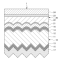
- FIG. 1 is a schematic cross-sectional view showing a solar cell according to one embodiment of the present invention
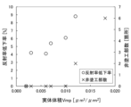
- FIG. 4 is a graph showing the reflectance decrease rate and the number of non-coated portions in processing examples of semiconductor substrates.
- FIG. 1 is a schematic cross-sectional view showing a solar cell 1 according to one embodiment of the invention.
- the solar cell 1 includes a crystalline silicon solar cell portion 10 and a perovskite solar cell portion 20 laminated on the light receiving surface side (surface side: upper side in FIG. 1) of the crystalline silicon solar cell portion 10 .
- the solar cell 1 is formed by connecting a crystalline silicon solar cell portion 10 and a perovskite solar cell portion 20 in series.
- incident light is photoelectrically converted in the perovskite solar cell section 20
- the light that has passed through the perovskite solar cell section 20 without being converted into electric power in the perovskite solar cell section 20 is converted in the crystalline silicon solar cell section 10 .
- By converting into electric power a relatively high photoelectric conversion efficiency is realized as a whole.
- the crystalline silicon solar cell unit 10 includes a semiconductor substrate 11, a first passivation layer 12 laminated on the first main surface of the semiconductor substrate 11 on the light receiving surface side, and a side opposite to the first main surface of the semiconductor substrate 11 (back side). : the second passivation layer 13 laminated on the second main surface (lower side in FIG. 1), the first semiconductor layer 14 laminated on the first passivation layer 12 and having the first conductivity, and the second passivation layer 13, a second semiconductor layer 15 having the second conductivity, an intermediate electrode layer 16 laminated on the first semiconductor layer 14, and a back electrode layer 17 laminated on the second semiconductor layer 15; can be configured to have
- the perovskite solar cell section 20 includes, from the crystalline silicon solar cell section 10 side, a first charge transport layer 21, an organic photoelectric conversion layer 22 laminated on the first charge transport layer 21, a second charge transport layer 23, a surface and the electrode layer 24 in this order.
- the semiconductor substrate 11 can be made of a crystalline silicon material such as monocrystalline silicon or polycrystalline silicon.
- the semiconductor substrate 11 may also be made of other semiconductor materials such as gallium arsenide (GaAs).
- Semiconductor substrate 11 may be an n-type semiconductor substrate, for example, a crystalline silicon material doped with an n-type dopant. Examples of n-type dopants include phosphorus (P).
- the semiconductor substrate 11 functions as a photoelectric conversion substrate that absorbs incident light from the light receiving surface side and generates photocarriers (electrons and holes). Since crystalline silicon is used as the material of the semiconductor substrate 11, dark current is relatively small, and relatively high output (stable output regardless of illuminance) can be obtained even when the intensity of incident light is low.
- the thickness of the semiconductor substrate 11 can be, for example, 50 ⁇ m or more and 300 ⁇ m or less.
- the semiconductor substrate 11 has an uneven structure having a plurality of projections with rounded tops on the first main surface.
- the semiconductor substrate 11 of this embodiment has a textured structure having a plurality of pyramid-shaped projections on the second main surface.
- the concave-convex structure of the first main surface of the semiconductor substrate 11 reduces the reflectance of light and increases the amount of light incident on the inside of the semiconductor substrate 11 , thereby increasing the photoelectric conversion efficiency of the crystalline silicon solar cell section 10 and thus the solar cell 1 . improve.
- the layer is laminated on the first principal surface or the first principal surface with a uniform thickness and has a surface shape that follows the first principal surface of the semiconductor substrate 11.
- pinholes are less likely to be formed in the coating film.
- the valleys of the concave-convex structure on the first main surface of the semiconductor substrate 11 may have a V-shaped cross section forming a clear bottom line as shown in FIG. 1, and are rounded like the tops. good too.
- the lower limit of the substantial volume Vmp at a load area ratio of 10% of the first principal surface is preferably 0.003 ⁇ m 3 / ⁇ m 2 , more preferably 0.005 ⁇ m 3 / ⁇ m 2 .
- the upper limit of the substantial volume Vmp at a load area ratio of 10% of the first main surface is preferably 0.010 ⁇ m 3 / ⁇ m 2 , more preferably 0.008 ⁇ m 3 / ⁇ m 2 .
- the “substantial volume Vmp” is the volume of the peaks measured in accordance with ISO25178, and the “loaded area ratio” is the load area at a certain height c (the area of the region with a height of c or more). percentage.
- the actual volume Vmp at a load area ratio of 10% of the first main surface By setting the actual volume Vmp at a load area ratio of 10% of the first main surface to be equal to or higher than the lower limit, the light reflectance is reduced more than when the first main surface is smooth, and the crystalline silicon solar cell section 10 is formed. Photoelectric conversion efficiency can be improved. Further, by setting the actual volume Vmp at the load area ratio of 10% of the first main surface to the above upper limit or less, it is possible to effectively suppress the formation of pinholes when the coating film is formed.
- the root-mean-square height Sq (ISO25178) of the uneven structure on the first main surface is, for example, 0.02 ⁇ m or more and 0.25 ⁇ m or less. Also, the number of protrusions per 10 ⁇ m square is, for example, 5 or more and 40 or less. By satisfying these conditions, it becomes easy to set the actual volume Vmp at a load area ratio of 10% of the first main surface within the above range.
- the concave-convex structure of the semiconductor substrate 11 is formed by anisotropically etching a crystalline silicon substrate having smooth first and second main surfaces to form a pyramidal texture structure on at least the first main surface, followed by the first By polishing the main surface, the top of the pyramidal texture can be formed by rounding. Polishing of the semiconductor substrate 11 is preferably performed by chemical mechanical polishing using a chemical solution that corrodes the semiconductor substrate 11 . As a result, the texture can be smoothly rounded, and the substantial volume Vmp at the load area ratio of 10% of the first principal surface can be made within the above range relatively easily.
- a mixed solution of nitric acid and hydrofluoric acid is preferably used as a chemical solution for chemical mechanical polishing of the semiconductor substrate 11 made of a crystalline silicon substrate.
- the textured structure of the second main surface of the semiconductor substrate 11 can be formed by anisotropically etching the crystalline silicon substrate. That is, unlike the first main surface, the second main surface of the semiconductor substrate 11 can be a non-polished surface.
- the second main surface side of the semiconductor substrate 11 is not coated in the manufacturing process of the solar cell 1, the second main surface has a textured structure, so that the light reflectance can be further lowered than that of the second main surface. .
- the textured structure is provided on the second main surface of the semiconductor substrate 11 to improve the utilization rate of light.
- the photoelectric conversion efficiency of the solar cell 1 can be further improved.
- anisotropically etching only one side of the crystalline silicon substrate in order to form the uneven structure on the first main surface of the semiconductor substrate 11 is more costly than anisotropically etching both sides.
- the first passivation layer 12 and the second passivation layer 13 suppress carrier recombination at the interface between the semiconductor substrate 11 and the first semiconductor layer 14 or the second semiconductor layer 15 .
- the first passivation layer 12 and the second passivation layer 13 can be intrinsic semiconductor thin layers formed from amorphous silicon.
- the first passivation layer 12 and the second passivation layer 13 can be laminated by a method such as sputtering, for example.
- the thickness of the first passivation layer 12 and the second passivation layer 13 can be, for example, 2 nm or more and 20 nm or less.
- the first semiconductor layer 14 and the second semiconductor layer 15 collect charges of different polarities by attracting carriers of different polarities from inside the semiconductor substrate 11 .
- the first semiconductor layer 14 may be formed from an n-type semiconductor
- the second semiconductor layer 15 may be formed from a p-type semiconductor.
- the first semiconductor layer 14 and the second semiconductor layer 15 can be formed, for example, of an amorphous silicon material containing a dopant that imparts a desired conductivity type.
- Examples of the p-type dopant include boron (B), and examples of the n-type dopant include phosphorus (P) described above.
- the intermediate electrode layer 16 is the electrode of the crystalline silicon solar cell section 10 and also serves as the electrode of the perovskite solar cell section 20 .
- the intermediate electrode layer 16 can be formed of a transparent conductive oxide (TCO) having electrical conductivity and light transparency so that light transmitted through the perovskite solar cell portion 20 is incident on the semiconductor substrate 11.
- TCO transparent conductive oxide
- the transparent conductive oxide forming the intermediate electrode layer 16 for example, indium oxide, tin oxide, zinc oxide, titanium oxide, composite oxides thereof, and the like can be used. Among these, an indium-based composite oxide containing indium oxide as a main component is preferable. Indium oxide is particularly preferred from the viewpoint of high electrical conductivity and transparency.
- dopants include Sn, W, Zn, Ti, Ce, Zr, Mo, Al, Ga, Ge, As, Si, S and the like.
- ITO Indium Tin Oxide
- the intermediate electrode layer 16 can be formed by a method such as sputtering or vacuum deposition.
- the thickness of the anode layer can be, for example, 5 nm or more and 100 nm or less.
- the back electrode layer 17 is one electrode for outputting electric power from the crystalline silicon solar cell section 10 and by extension the solar cell 1 .
- the back electrode layer 17 can be made of a conductive material such as a transparent conductive oxide such as ITO, a cured conductive paste such as silver paste, or a metal such as Cu or Ni.
- the back electrode layer 17 may have a multi-layer structure. and a layer formed from a paste.
- a method for forming the back electrode layer 17 is selected according to the material thereof, and methods such as sputtering, coating, and plating can be used.
- the thickness of the back electrode layer 17 can be, for example, 100 nm or more and 300 nm or less.
- the first charge transport layer 21 is a hole transport layer (HTL) that selectively transfers carriers generated in the organic photoelectric conversion layer 22 , or holes in the present embodiment, to the intermediate electrode layer 16 .
- HTL hole transport layer
- metal oxides such as nickel oxide (NiO) and copper oxide (Cu 2 O), for example, PTAA (Poly(bis(4-phenyl) (2,4,6-trimethylphenyl)amine)) and Spiro-MeOTAD.
- the first charge transport layer 21 includes, for example, 2PACz ([2-(9H-Carbazol-9-yl)ethyl]phosphonic Acid), MeO-2PACz ([2-(3,6-Dimethoxy-9H-carbazol-9 SAM: Self-Assembled Monolayers).
- the first charge transport layer 21 made of metal oxide can be formed by a method such as sputtering or vacuum deposition.
- the first charge transport layer 21 containing an organic substance can be formed by a method such as applying a solution of an organic substance and drying it.
- a coating film having no pinholes can be formed by reducing the actual volume Vmp of the semiconductor substrate 11 as described above. The formation of defects in the perovskite solar cell portion 20 is prevented, and the photoelectric conversion efficiency of the perovskite solar cell portion 20 and thus the solar cell 1 can be improved.
- the thickness of the first charge transport layer 21 may vary greatly depending on its material, the structure of adjacent layers, and the like. thickness.
- the organic photoelectric conversion layer 22 contains a perovskite compound and absorbs light to generate carriers.
- the perovskite compound contained in the organic photoelectric conversion layer 22 includes an organic atom A containing at least one of monovalent organic ammonium ions and amidinium ions, a metal atom B that generates divalent metal ions, and iodide.
- a compound represented by ABX 3 containing a halogen atom X containing at least one of ion I, bromide ion Br, chloride ion Cl, and fluoride ion F can be used.
- the organic photoelectric conversion layer 22 can be formed by, for example, a vapor deposition method or the like, but a sol-gel method of applying a solution (a method of synthesizing a perovskite compound in a coating film), a coating method (a solution containing a pre-synthesized perovskite compound It is assumed to be formed by a method such as a method of applying a When the organic photoelectric conversion layer 22 is formed by applying a solution, by reducing the actual volume Vmp of the semiconductor substrate 11 as described above, the organic photoelectric conversion layer 22 can be formed without pinholes and uneven distribution of perovskite compounds. The photoelectric conversion efficiency of the solar cell unit 20 and thus the solar cell 1 can be improved.
- the thickness of the organic photoelectric conversion layer 22 is preferably 100 nm or more and 1000 nm or less in order to increase the light absorptivity and reduce the movement distance of generated charges, although it depends on the material used for forming the layer.
- the second charge transport layer 23 is an electron transport layer (ETL) that selectively transfers carriers generated in the organic photoelectric conversion layer 22 , electrons in this embodiment, to the surface electrode layer 24 .
- ETL electron transport layer
- the main material of the second charge transport layer 23, which is an electron transport layer include PTAA (Poly(bis(4-phenyl)(2,4,6-trimethylphenyl)amine)), Spiro-MeOTAD, and fullerene. be done.
- Fullerenes include, for example, C60, C70, hydrides, oxides, metal complexes, and derivatives to which an alkyl group or the like is added.
- the second charge transport layer 23 can be formed by, for example, a sol-gel method, a coating method, or the like.
- the thickness of the second charge transport layer 23 can be, for example, 3 nm or more and 30 nm or less.
- the surface electrode layer 24 is an electrode paired with the intermediate electrode layer 16 in the perovskite solar cell section 20 .
- the surface electrode layer 24 is a transparent electrode that transmits incident light through the antireflection layer 33 , and can be formed using the same material as the intermediate electrode layer 16 by the same method as the intermediate electrode layer 16 .
- the thickness of the surface electrode layer 24 may be, for example, 500 nm or more and 1000 nm or less.
- the substantial volume Vmp of the first main surface of the semiconductor substrate 11 is within the range described above, so that the coating when forming the first charge transport layer 21 and the organic photoelectric conversion layer 22 is Due to good workability, there are few defects and the photoelectric conversion efficiency is excellent.
- the present invention is not limited to the above-described embodiments, and various changes and modifications are possible.
- the surface shape of the second main surface of the semiconductor substrate is not particularly limited, and may have an uneven structure having the same substantial volume Vmp as that of the first main surface. It may be mirror-like.
- a solar cell according to the present invention may be one without some layers, such as the perovskite solar cell portion, or may have further layers, such as an anti-reflection layer, laminated to the light-receiving surface.
- the solar cell according to the present invention may be a so-called back electrode type solar cell in which the first semiconductor layer and the second semiconductor layer are provided in complementary shapes on the back side of the semiconductor substrate.
- the first main surface having the above-described substantial volume Vmp may be the surface opposite to the light receiving surface.
- the present invention can be used to pattern the first semiconductor layer and the second semiconductor layer. The absorptance of light from the back side can be improved while facilitating the formation of a resist or the like.
- a mirror-finished crystalline silicon substrate (substrate number 1), a substrate having a texture structure formed on the same crystalline silicon substrate by anisotropic etching (substrate numbers 2 to 4), and the surface having the texture structure formed thereon was polished by chemical mechanical polishing.
- Semiconductor substrates (substrate numbers 5 to 8) were fabricated. For each semiconductor substrate, the actual volume Vmp at a load area ratio of 10% and the reduction rate of the reflectance of light at a wavelength of 800 nm from the mirror substrate were measured. Further, after coating each semiconductor substrate with a solution containing a perovskite compound, the surface was observed with a microscope to count the number of uncoated portions (pinholes) within a 50 ⁇ m square region. The following table shows the results of these measurements.
- the graph in FIG. 2 shows the actual volume Vmp and the reflectance decrease rate in the range where the actual volume Vmp is small.
- the actual volume Vmp As shown in the figure, by setting the actual volume Vmp to 0.003 or more, it is considered that the reflectance can be reduced and the photoelectric conversion efficiency of the solar cell can be improved as compared with the mirror-finished crystalline silicon substrate. Also, by setting the actual volume Vmp to 0.010 or less, defects do not occur in the coating film, so it is thought that a decrease in photoelectric conversion efficiency due to manufacturing defects in the solar cell can be prevented.
Landscapes
- Physics & Mathematics (AREA)
- Electromagnetism (AREA)
- Chemical & Material Sciences (AREA)
- Engineering & Computer Science (AREA)
- Materials Engineering (AREA)
- Inorganic Chemistry (AREA)
- Photovoltaic Devices (AREA)
Abstract
Description

10 結晶シリコン太陽電池部
11 半導体基板
12 第1パッシベーション層
13 第2パッシベーション層
14 第1半導体層
15 第2半導体層
16 中間電極層
17 裏面電極層
20 ペロブスカイト太陽電池部
21 第1電荷輸送層
22 有機光電変換層
23 第2電荷輸送層
24 表面電極層
Claims (5)
- 半導体基板と、
前記半導体基板に積層される、第1の導電性を有する第1半導体層及び第2の導電性を有する第2半導体層と、
を備え、
前記半導体基板の少なくとも第1主面の負荷面積率10%における実体体積Vmpが0.003μm3/μm2以上0.010μm3/μm2以下である、太陽電池。 - 前記第1半導体層と前記第2半導体層とは、互いに異なる主面に積層される、請求項1に記載の太陽電池。
- 前記第1主面側に積層され、ペロブスカイト化合物を含む有機光電変換層をさらに備える、請求項2に記載の太陽電池。
- 前記第1主面側から受光する、請求項1から3のいずれかに記載の太陽電池。
- 前記半導体基板の第2主面に複数のピラミッド状の突起を有するテクスチャ構造を有する、請求項1から4のいずれかに記載の太陽電池。
Priority Applications (4)
| Application Number | Priority Date | Filing Date | Title |
|---|---|---|---|
| EP22869761.1A EP4404280A4 (en) | 2021-09-14 | 2022-08-23 | SOLAR CELL |
| JP2023548378A JPWO2023042614A1 (ja) | 2021-09-14 | 2022-08-23 | |
| CN202280061642.5A CN117981092A (zh) | 2021-09-14 | 2022-08-23 | 太阳能电池 |
| US18/603,645 US20240224550A1 (en) | 2021-09-14 | 2024-03-13 | Solar cell |
Applications Claiming Priority (2)
| Application Number | Priority Date | Filing Date | Title |
|---|---|---|---|
| JP2021149306 | 2021-09-14 | ||
| JP2021-149306 | 2021-09-14 |
Related Child Applications (1)
| Application Number | Title | Priority Date | Filing Date |
|---|---|---|---|
| US18/603,645 Continuation US20240224550A1 (en) | 2021-09-14 | 2024-03-13 | Solar cell |
Publications (1)
| Publication Number | Publication Date |
|---|---|
| WO2023042614A1 true WO2023042614A1 (ja) | 2023-03-23 |
Family
ID=85602779
Family Applications (1)
| Application Number | Title | Priority Date | Filing Date |
|---|---|---|---|
| PCT/JP2022/031723 Ceased WO2023042614A1 (ja) | 2021-09-14 | 2022-08-23 | 太陽電池 |
Country Status (5)
| Country | Link |
|---|---|
| US (1) | US20240224550A1 (ja) |
| EP (1) | EP4404280A4 (ja) |
| JP (1) | JPWO2023042614A1 (ja) |
| CN (1) | CN117981092A (ja) |
| WO (1) | WO2023042614A1 (ja) |
Families Citing this family (1)
| Publication number | Priority date | Publication date | Assignee | Title |
|---|---|---|---|---|
| CN119836108B (zh) * | 2025-01-07 | 2025-11-21 | 凤阳硅谷智能有限公司 | 一种高透光型的钙钛矿电池结构及其制作方法 |
Citations (9)
| Publication number | Priority date | Publication date | Assignee | Title |
|---|---|---|---|---|
| JP2014229876A (ja) * | 2013-05-27 | 2014-12-08 | 株式会社カネカ | 結晶シリコン系太陽電池およびその製造方法、ならびに太陽電池モジュール |
| WO2017195722A1 (ja) * | 2016-05-09 | 2017-11-16 | 株式会社カネカ | 積層型光電変換装置およびその製造方法 |
| WO2017200000A1 (ja) * | 2016-05-17 | 2017-11-23 | 積水化学工業株式会社 | 固体接合型光電変換素子、及びその製造方法 |
| JP2018163959A (ja) | 2017-03-24 | 2018-10-18 | 株式会社カネカ | 太陽電池モジュールおよび光電変換素子の製造方法 |
| WO2020105289A1 (ja) * | 2018-11-19 | 2020-05-28 | 三井金属鉱業株式会社 | 表面処理銅箔、キャリア付銅箔、銅張積層板及びプリント配線板 |
| JP2020082453A (ja) * | 2018-11-21 | 2020-06-04 | 日本メクトロン株式会社 | 導体張積層板及び導体張積層板の製造方法 |
| WO2020130318A1 (ko) | 2018-12-18 | 2020-06-25 | 엘지전자 주식회사 | 텐덤 태양전지 |
| US20200212243A1 (en) * | 2017-05-29 | 2020-07-02 | Lg Electronics Inc. | Method for manufacturing perovskite silicon tandem solar cell |
| JP2021057435A (ja) | 2019-09-30 | 2021-04-08 | パナソニック株式会社 | 太陽電池セルおよび太陽電池セルの製造方法 |
-
2022
- 2022-08-23 JP JP2023548378A patent/JPWO2023042614A1/ja active Pending
- 2022-08-23 EP EP22869761.1A patent/EP4404280A4/en active Pending
- 2022-08-23 WO PCT/JP2022/031723 patent/WO2023042614A1/ja not_active Ceased
- 2022-08-23 CN CN202280061642.5A patent/CN117981092A/zh active Pending
-
2024
- 2024-03-13 US US18/603,645 patent/US20240224550A1/en active Pending
Patent Citations (9)
| Publication number | Priority date | Publication date | Assignee | Title |
|---|---|---|---|---|
| JP2014229876A (ja) * | 2013-05-27 | 2014-12-08 | 株式会社カネカ | 結晶シリコン系太陽電池およびその製造方法、ならびに太陽電池モジュール |
| WO2017195722A1 (ja) * | 2016-05-09 | 2017-11-16 | 株式会社カネカ | 積層型光電変換装置およびその製造方法 |
| WO2017200000A1 (ja) * | 2016-05-17 | 2017-11-23 | 積水化学工業株式会社 | 固体接合型光電変換素子、及びその製造方法 |
| JP2018163959A (ja) | 2017-03-24 | 2018-10-18 | 株式会社カネカ | 太陽電池モジュールおよび光電変換素子の製造方法 |
| US20200212243A1 (en) * | 2017-05-29 | 2020-07-02 | Lg Electronics Inc. | Method for manufacturing perovskite silicon tandem solar cell |
| WO2020105289A1 (ja) * | 2018-11-19 | 2020-05-28 | 三井金属鉱業株式会社 | 表面処理銅箔、キャリア付銅箔、銅張積層板及びプリント配線板 |
| JP2020082453A (ja) * | 2018-11-21 | 2020-06-04 | 日本メクトロン株式会社 | 導体張積層板及び導体張積層板の製造方法 |
| WO2020130318A1 (ko) | 2018-12-18 | 2020-06-25 | 엘지전자 주식회사 | 텐덤 태양전지 |
| JP2021057435A (ja) | 2019-09-30 | 2021-04-08 | パナソニック株式会社 | 太陽電池セルおよび太陽電池セルの製造方法 |
Non-Patent Citations (1)
| Title |
|---|
| See also references of EP4404280A4 |
Also Published As
| Publication number | Publication date |
|---|---|
| JPWO2023042614A1 (ja) | 2023-03-23 |
| EP4404280A1 (en) | 2024-07-24 |
| US20240224550A1 (en) | 2024-07-04 |
| EP4404280A4 (en) | 2025-09-03 |
| CN117981092A (zh) | 2024-05-03 |
Similar Documents
| Publication | Publication Date | Title |
|---|---|---|
| JP7755065B2 (ja) | ペロブスカイト-シリコンベースの積層太陽電池及びその製造方法 | |
| CN109196678B (zh) | 层叠型光电转换装置和其制造方法 | |
| US10672930B2 (en) | Photoelectric conversion device and photoelectric conversion module | |
| CN103700713B (zh) | 太阳能电池及其制造方法 | |
| WO2022073518A1 (zh) | 一种叠层电池及其制作方法 | |
| JP2023538427A (ja) | タンデム型太陽電池 | |
| KR20180130396A (ko) | 페로브스카이트 실리콘 탠덤 태양전지 및 제조 방법 | |
| TW201547044A (zh) | 在太陽能電池後側之導電聚合物/Si之界面 | |
| US20180019361A1 (en) | Photoelectric conversion device, manufacturing method for photoelectric conversion device, and photoelectric conversion module | |
| CN112086534B (zh) | 一种叠层电池及其制作方法 | |
| EP4597584A1 (en) | Bi-facial light-receiving silicon/perovskite tandem solar cell | |
| Li et al. | Nanoscale Size Control of Si Pyramid Texture for Perovskite/Si Tandem Solar Cells Enabling Solution‐Based Perovskite Top‐Cell Fabrication and Improved Si Bottom‐Cell Response | |
| CN112054068A (zh) | 硅异质结太阳能电池及其制作方法 | |
| TW201413986A (zh) | 太陽能電池 | |
| JP2014192370A (ja) | 結晶シリコン太陽電池、およびその製造方法、ならびに太陽電池モジュール | |
| CN212323018U (zh) | 一种叠层电池结构 | |
| US20240224550A1 (en) | Solar cell | |
| WO2025249111A1 (ja) | タンデム型太陽電池、およびその製造方法 | |
| JP2002319688A (ja) | 積層型太陽電池 | |
| WO2025018250A1 (ja) | タンデム型太陽電池、タンデム型太陽電池の製造方法 | |
| KR20200061479A (ko) | 전하선택 박막을 포함하는 실리콘 태양전지 및 이의 제조방법 | |
| KR20090110048A (ko) | 투명 도전막, 이를 이용한 태양전지 및 이의 제조 방법 | |
| CN120603331B (zh) | 一种低紫外衰减晶硅异质结太阳能电池及其制备方法 | |
| KR101303594B1 (ko) | 표면 텍스처가 형성된 유리기판을 이용한 박막형 태양전지 및 이의 제조방법 | |
| CN120659433B (zh) | 晶硅绒面结构、电池及其制备方法、光伏组件 |
Legal Events
| Date | Code | Title | Description |
|---|---|---|---|
| 121 | Ep: the epo has been informed by wipo that ep was designated in this application |
Ref document number: 22869761 Country of ref document: EP Kind code of ref document: A1 |
|
| WWE | Wipo information: entry into national phase |
Ref document number: 2023548378 Country of ref document: JP |
|
| WWE | Wipo information: entry into national phase |
Ref document number: 202280061642.5 Country of ref document: CN |
|
| WWE | Wipo information: entry into national phase |
Ref document number: 2022869761 Country of ref document: EP |
|
| NENP | Non-entry into the national phase |
Ref country code: DE |
|
| ENP | Entry into the national phase |
Ref document number: 2022869761 Country of ref document: EP Effective date: 20240415 |