WO2023047765A1 - 金属-セラミックス接合基板およびその製造方法 - Google Patents
金属-セラミックス接合基板およびその製造方法 Download PDFInfo
- Publication number
- WO2023047765A1 WO2023047765A1 PCT/JP2022/027275 JP2022027275W WO2023047765A1 WO 2023047765 A1 WO2023047765 A1 WO 2023047765A1 JP 2022027275 W JP2022027275 W JP 2022027275W WO 2023047765 A1 WO2023047765 A1 WO 2023047765A1
- Authority
- WO
- WIPO (PCT)
- Prior art keywords
- metal
- circuit board
- ceramic
- brazing material
- metal plate
- Prior art date
- Legal status (The legal status is an assumption and is not a legal conclusion. Google has not performed a legal analysis and makes no representation as to the accuracy of the status listed.)
- Ceased
Links
Images


Classifications
-
- H—ELECTRICITY
- H10—SEMICONDUCTOR DEVICES; ELECTRIC SOLID-STATE DEVICES NOT OTHERWISE PROVIDED FOR
- H10W—GENERIC PACKAGES, INTERCONNECTIONS, CONNECTORS OR OTHER CONSTRUCTIONAL DETAILS OF DEVICES COVERED BY CLASS H10
- H10W70/00—Package substrates; Interposers; Redistribution layers [RDL]
- H10W70/60—Insulating or insulated package substrates; Interposers; Redistribution layers
-
- H—ELECTRICITY
- H10—SEMICONDUCTOR DEVICES; ELECTRIC SOLID-STATE DEVICES NOT OTHERWISE PROVIDED FOR
- H10W—GENERIC PACKAGES, INTERCONNECTIONS, CONNECTORS OR OTHER CONSTRUCTIONAL DETAILS OF DEVICES COVERED BY CLASS H10
- H10W70/00—Package substrates; Interposers; Redistribution layers [RDL]
- H10W70/40—Leadframes
- H10W70/461—Leadframes specially adapted for cooling
-
- C—CHEMISTRY; METALLURGY
- C04—CEMENTS; CONCRETE; ARTIFICIAL STONE; CERAMICS; REFRACTORIES
- C04B—LIME, MAGNESIA; SLAG; CEMENTS; COMPOSITIONS THEREOF, e.g. MORTARS, CONCRETE OR LIKE BUILDING MATERIALS; ARTIFICIAL STONE; CERAMICS; REFRACTORIES; TREATMENT OF NATURAL STONE
- C04B37/00—Joining burned ceramic articles with other burned ceramic articles or other articles by heating
- C04B37/02—Joining burned ceramic articles with other burned ceramic articles or other articles by heating with metallic articles
- C04B37/023—Joining burned ceramic articles with other burned ceramic articles or other articles by heating with metallic articles characterised by the interlayer used
- C04B37/026—Joining burned ceramic articles with other burned ceramic articles or other articles by heating with metallic articles characterised by the interlayer used consisting of metals or metal salts
-
- H—ELECTRICITY
- H05—ELECTRIC TECHNIQUES NOT OTHERWISE PROVIDED FOR
- H05K—PRINTED CIRCUITS; CASINGS OR CONSTRUCTIONAL DETAILS OF ELECTRIC APPARATUS; MANUFACTURE OF ASSEMBLAGES OF ELECTRICAL COMPONENTS
- H05K3/00—Apparatus or processes for manufacturing printed circuits
- H05K3/02—Apparatus or processes for manufacturing printed circuits in which the conductive material is applied to the surface of the insulating support and is thereafter removed from such areas of the surface which are not intended for current conducting or shielding
- H05K3/06—Apparatus or processes for manufacturing printed circuits in which the conductive material is applied to the surface of the insulating support and is thereafter removed from such areas of the surface which are not intended for current conducting or shielding the conductive material being removed chemically or electrolytically, e.g. by photo-etch process
-
- H—ELECTRICITY
- H10—SEMICONDUCTOR DEVICES; ELECTRIC SOLID-STATE DEVICES NOT OTHERWISE PROVIDED FOR
- H10W—GENERIC PACKAGES, INTERCONNECTIONS, CONNECTORS OR OTHER CONSTRUCTIONAL DETAILS OF DEVICES COVERED BY CLASS H10
- H10W40/00—Arrangements for thermal protection or thermal control
- H10W40/20—Arrangements for cooling
- H10W40/25—Arrangements for cooling characterised by their materials
- H10W40/255—Arrangements for cooling characterised by their materials having a laminate or multilayered structure, e.g. direct bond copper [DBC] ceramic substrates
-
- H—ELECTRICITY
- H10—SEMICONDUCTOR DEVICES; ELECTRIC SOLID-STATE DEVICES NOT OTHERWISE PROVIDED FOR
- H10W—GENERIC PACKAGES, INTERCONNECTIONS, CONNECTORS OR OTHER CONSTRUCTIONAL DETAILS OF DEVICES COVERED BY CLASS H10
- H10W70/00—Package substrates; Interposers; Redistribution layers [RDL]
- H10W70/01—Manufacture or treatment
- H10W70/04—Manufacture or treatment of leadframes
- H10W70/047—Attaching leadframes to insulating supports, e.g. for tape automated bonding [TAB]
-
- H—ELECTRICITY
- H10—SEMICONDUCTOR DEVICES; ELECTRIC SOLID-STATE DEVICES NOT OTHERWISE PROVIDED FOR
- H10W—GENERIC PACKAGES, INTERCONNECTIONS, CONNECTORS OR OTHER CONSTRUCTIONAL DETAILS OF DEVICES COVERED BY CLASS H10
- H10W70/00—Package substrates; Interposers; Redistribution layers [RDL]
- H10W70/60—Insulating or insulated package substrates; Interposers; Redistribution layers
- H10W70/67—Insulating or insulated package substrates; Interposers; Redistribution layers characterised by their insulating layers or insulating parts
- H10W70/68—Shapes or dispositions thereof
-
- H—ELECTRICITY
- H10—SEMICONDUCTOR DEVICES; ELECTRIC SOLID-STATE DEVICES NOT OTHERWISE PROVIDED FOR
- H10W—GENERIC PACKAGES, INTERCONNECTIONS, CONNECTORS OR OTHER CONSTRUCTIONAL DETAILS OF DEVICES COVERED BY CLASS H10
- H10W99/00—Subject matter not provided for in other groups of this subclass
-
- C—CHEMISTRY; METALLURGY
- C04—CEMENTS; CONCRETE; ARTIFICIAL STONE; CERAMICS; REFRACTORIES
- C04B—LIME, MAGNESIA; SLAG; CEMENTS; COMPOSITIONS THEREOF, e.g. MORTARS, CONCRETE OR LIKE BUILDING MATERIALS; ARTIFICIAL STONE; CERAMICS; REFRACTORIES; TREATMENT OF NATURAL STONE
- C04B2237/00—Aspects relating to ceramic laminates or to joining of ceramic articles with other articles by heating
- C04B2237/02—Aspects relating to interlayers, e.g. used to join ceramic articles with other articles by heating
- C04B2237/12—Metallic interlayers
- C04B2237/124—Metallic interlayers based on copper
-
- C—CHEMISTRY; METALLURGY
- C04—CEMENTS; CONCRETE; ARTIFICIAL STONE; CERAMICS; REFRACTORIES
- C04B—LIME, MAGNESIA; SLAG; CEMENTS; COMPOSITIONS THEREOF, e.g. MORTARS, CONCRETE OR LIKE BUILDING MATERIALS; ARTIFICIAL STONE; CERAMICS; REFRACTORIES; TREATMENT OF NATURAL STONE
- C04B2237/00—Aspects relating to ceramic laminates or to joining of ceramic articles with other articles by heating
- C04B2237/02—Aspects relating to interlayers, e.g. used to join ceramic articles with other articles by heating
- C04B2237/12—Metallic interlayers
- C04B2237/125—Metallic interlayers based on noble metals, e.g. silver
-
- C—CHEMISTRY; METALLURGY
- C04—CEMENTS; CONCRETE; ARTIFICIAL STONE; CERAMICS; REFRACTORIES
- C04B—LIME, MAGNESIA; SLAG; CEMENTS; COMPOSITIONS THEREOF, e.g. MORTARS, CONCRETE OR LIKE BUILDING MATERIALS; ARTIFICIAL STONE; CERAMICS; REFRACTORIES; TREATMENT OF NATURAL STONE
- C04B2237/00—Aspects relating to ceramic laminates or to joining of ceramic articles with other articles by heating
- C04B2237/02—Aspects relating to interlayers, e.g. used to join ceramic articles with other articles by heating
- C04B2237/12—Metallic interlayers
- C04B2237/126—Metallic interlayers wherein the active component for bonding is not the largest fraction of the interlayer
- C04B2237/127—The active component for bonding being a refractory metal
-
- C—CHEMISTRY; METALLURGY
- C04—CEMENTS; CONCRETE; ARTIFICIAL STONE; CERAMICS; REFRACTORIES
- C04B—LIME, MAGNESIA; SLAG; CEMENTS; COMPOSITIONS THEREOF, e.g. MORTARS, CONCRETE OR LIKE BUILDING MATERIALS; ARTIFICIAL STONE; CERAMICS; REFRACTORIES; TREATMENT OF NATURAL STONE
- C04B2237/00—Aspects relating to ceramic laminates or to joining of ceramic articles with other articles by heating
- C04B2237/30—Composition of layers of ceramic laminates or of ceramic or metallic articles to be joined by heating, e.g. Si substrates
- C04B2237/32—Ceramic
- C04B2237/36—Non-oxidic
- C04B2237/366—Aluminium nitride
-
- C—CHEMISTRY; METALLURGY
- C04—CEMENTS; CONCRETE; ARTIFICIAL STONE; CERAMICS; REFRACTORIES
- C04B—LIME, MAGNESIA; SLAG; CEMENTS; COMPOSITIONS THEREOF, e.g. MORTARS, CONCRETE OR LIKE BUILDING MATERIALS; ARTIFICIAL STONE; CERAMICS; REFRACTORIES; TREATMENT OF NATURAL STONE
- C04B2237/00—Aspects relating to ceramic laminates or to joining of ceramic articles with other articles by heating
- C04B2237/30—Composition of layers of ceramic laminates or of ceramic or metallic articles to be joined by heating, e.g. Si substrates
- C04B2237/40—Metallic
- C04B2237/407—Copper
-
- H—ELECTRICITY
- H05—ELECTRIC TECHNIQUES NOT OTHERWISE PROVIDED FOR
- H05K—PRINTED CIRCUITS; CASINGS OR CONSTRUCTIONAL DETAILS OF ELECTRIC APPARATUS; MANUFACTURE OF ASSEMBLAGES OF ELECTRICAL COMPONENTS
- H05K1/00—Printed circuits
- H05K1/02—Details
- H05K1/03—Use of materials for the substrate
- H05K1/0306—Inorganic insulating substrates, e.g. ceramic, glass
-
- H—ELECTRICITY
- H05—ELECTRIC TECHNIQUES NOT OTHERWISE PROVIDED FOR
- H05K—PRINTED CIRCUITS; CASINGS OR CONSTRUCTIONAL DETAILS OF ELECTRIC APPARATUS; MANUFACTURE OF ASSEMBLAGES OF ELECTRICAL COMPONENTS
- H05K2201/00—Indexing scheme relating to printed circuits covered by H05K1/00
- H05K2201/09—Shape and layout
- H05K2201/09209—Shape and layout details of conductors
- H05K2201/09654—Shape and layout details of conductors covering at least two types of conductors provided for in H05K2201/09218 - H05K2201/095
- H05K2201/098—Special shape of the cross-section of conductors, e.g. very thick plated conductors
-
- H—ELECTRICITY
- H05—ELECTRIC TECHNIQUES NOT OTHERWISE PROVIDED FOR
- H05K—PRINTED CIRCUITS; CASINGS OR CONSTRUCTIONAL DETAILS OF ELECTRIC APPARATUS; MANUFACTURE OF ASSEMBLAGES OF ELECTRICAL COMPONENTS
- H05K2203/00—Indexing scheme relating to apparatus or processes for manufacturing printed circuits covered by H05K3/00
- H05K2203/14—Related to the order of processing steps
- H05K2203/1476—Same or similar kind of process performed in phases, e.g. coarse patterning followed by fine patterning
-
- H—ELECTRICITY
- H05—ELECTRIC TECHNIQUES NOT OTHERWISE PROVIDED FOR
- H05K—PRINTED CIRCUITS; CASINGS OR CONSTRUCTIONAL DETAILS OF ELECTRIC APPARATUS; MANUFACTURE OF ASSEMBLAGES OF ELECTRICAL COMPONENTS
- H05K3/00—Apparatus or processes for manufacturing printed circuits
- H05K3/22—Secondary treatment of printed circuits
- H05K3/28—Applying non-metallic protective coatings
Definitions
- the present invention relates to a metal-ceramic bonded (circuit) substrate and its manufacturing method, and more particularly to a metal-ceramic bonded substrate in which a metal circuit is bonded to a ceramic substrate with a brazing material, and its manufacturing method.
- power modules are used to control high power in electric vehicles, trains, and machine tools.
- an insulating substrate for such a power module there is a metal-ceramic bonded substrate in which chip parts on a metal circuit board bonded to one side of a ceramic substrate and portions requiring soldering of terminals are plated. It is used.
- the working voltage is as high as 6 to 9 kV, and accordingly the metal-ceramic bonding substrates used are required to be highly reliable and able to withstand such voltages with a margin. It is If the amount of partial discharge charge increases when a high voltage is applied, dielectric breakdown may occur. Partial discharge can be suppressed by increasing the insulation distance (distance between circuit patterns, creepage distance). There is a problem of becoming In addition, in such a metal-ceramic bonded substrate, cracks are likely to occur in the ceramic substrate due to thermal stress caused by the difference in thermal expansion between the ceramic substrate and the metal circuit board due to thermal shock after bonding.
- a method of thinning the creeping surface of the metal circuit board namely, a stepped structure or a fillet of brazing material (for joining the metal circuit board to the ceramic substrate) is applied to the peripheral edge of the metal circuit board.
- a method of forming a protruding portion of the brazing material is known.
- Patent Document 1 a solid insulating film is formed on the upper surface of the insulating substrate in contact with the outer peripheral edge of the conductive film of the circuit substrate.
- a high voltage such as 6 to 9 kV can be obtained by applying a coating material to a bonding substrate having a brazing material protrusion (fillet). It is said to have sufficient durability against withstand voltage and partial discharge characteristics.
- Patent Document 1 has good partial discharge characteristics by inserting an insulating substrate into a mold and filling it with a resin, but it is inferior in heat cycle resistance characteristics and the cost of resin filling is high. Further, the technique disclosed in Patent Document 2 has a maximum partial discharge characteristic of about 9 kV, which is not sufficient.
- An object of the present invention is to solve these problems and to provide a metal-ceramic bonded substrate with good partial discharge characteristics, excellent heat cycle resistance and heat resistance, and a method for manufacturing the same.
- a metal-ceramic bonding substrate in which a metal circuit board is bonded to one surface of a ceramic substrate via a brazing material layer, wherein the side surface of the metal circuit board is A protruding portion of the brazing material layer that protrudes outward from the lower end portion by 80 ⁇ m or more is formed, the side surface of the metal circuit board has an angle of 75° or more with respect to the surface of the ceramic substrate, and the side surface of the metal circuit board and a metal-ceramic bonding substrate in which the protruding portion of the brazing material layer is covered with an insulating layer.
- a heat radiation side metal plate may be joined to the other surface of the ceramic substrate.
- the metal plate on the heat radiation side may be made of copper or a copper alloy.
- the metal circuit board may be made of copper or a copper alloy.
- Nickel plating or nickel alloy plating may be formed on the surfaces of the protruding portions of the metal circuit board and the brazing material layer.
- resin may be sufficient as the said insulating layer. In that case, the resin may contain a polyimide resin as a main component.
- a metal-ceramic bonded body in which a metal plate is bonded to one surface of a ceramic substrate via a brazing material layer, an unnecessary portion of the metal plate is removed to form a metal circuit board. Then, the brazing material layer protrudes from the lower end of the side surface of the metal circuit board by 80 ⁇ m or more to form a protruding part of the brazing material layer, and the side surface of the metal circuit board is 75° to the surface of the ceramic substrate.
- a method for manufacturing a metal-ceramic bonding substrate comprising etching the side surface of a metal circuit board so as to form the above angle, and then forming an insulating layer so as to cover the side surface of the metal circuit board and the protruding portion of the brazing material layer. is provided.
- a metal-ceramic bonded body in which a metal plate is bonded to one surface of a ceramic substrate via a brazing filler metal layer and a metal plate is bonded to the other surface via a heat radiating brazing filler metal layer,
- the metal plate and unnecessary portions of the metal plate on the other side may be removed, and a metal circuit board may be formed on one side of the ceramic substrate, and a heat radiation side metal plate may be formed on the other side.
- the metal plate on the heat radiation side may be made of copper or a copper alloy.
- the metal circuit board may be made of copper or a copper alloy.
- nickel or nickel alloy plating may be formed on the surfaces of the metal circuit board and the protruding portion of the brazing material.
- the insulating layer may be formed by applying a coating material made of an insulating resin and then curing the coating material. In that case, the resin may contain a polyimide resin as a main component.
- the present invention it is possible to provide a metal-ceramic bonded substrate having good partial discharge characteristics, excellent heat cycle resistance and heat resistance, and a method for producing the same.
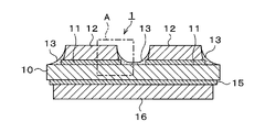
- FIG. 1 is a cross-sectional view showing a metal-ceramic bonding substrate according to an embodiment of the present invention
- FIG. FIG. 2 is an enlarged cross-sectional view of a portion A in FIG. 1
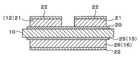
- FIG. 1 is an explanatory diagram showing an example of a method for manufacturing a metal-ceramic bonding substrate according to an embodiment of the present invention, showing a state in which paste-like active metal-containing brazing filler metal is applied to both surfaces of a ceramic substrate by screen printing.
- 1 is an explanatory view showing an example of a method for manufacturing a metal-ceramic bonded substrate according to an embodiment of the present invention, showing a state in which a ceramic substrate and a metal plate are bonded via an active metal-containing brazing filler metal;
- FIG. 1 is an explanatory view showing an example of a method for manufacturing a metal-ceramic bonded substrate according to an embodiment of the present invention, wherein a desired circuit pattern shape and heat radiation side metal plate are formed on the surfaces of the metal plates bonded to the upper and lower surfaces of the ceramic substrate. The state which applied the resist of the shape is shown.
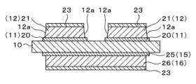
- 1 is an explanatory view showing an example of a method for manufacturing a metal-ceramic bonded substrate according to an embodiment of the present invention, showing a state in which unnecessary portions of a metal plate are removed by etching; FIG. FIG.
- FIG. 2 is an explanatory view showing an example of a method for manufacturing a metal-ceramic bonded substrate according to an embodiment of the present invention, showing a state where the resist is removed after unnecessary portions of the metal plate are removed by etching.
- 1 is an explanatory view showing an example of a method for manufacturing a metal-ceramic bonding substrate according to an embodiment of the present invention, showing a state in which an unnecessary portion of an active metal-containing brazing filler metal is removed;
- FIG. FIG. 2 is an explanatory diagram showing an example of a method for manufacturing a metal-ceramic bonded substrate according to an embodiment of the present invention, showing a state in which a resist is applied to substantially the entire upper surface (surface) of a metal plate;
- FIG. 1 is an explanatory diagram showing an example of a method for manufacturing a metal-ceramic bonded substrate according to an embodiment of the present invention, in which the side surface of a metal plate (periphery of the metal plate) is removed by etching to form an active metal-containing brazing material on the metal plate. It shows a state where it protrudes from the side part.
- FIG. 1 is an explanatory diagram showing an example of a method for manufacturing a metal-ceramic bonded substrate according to an embodiment of the present invention, in which the side surface of a metal plate (periphery of the metal plate) is removed by etching to form an active metal-containing brazing material on the metal plate. After protruding from the side portion, the resist is removed.
- FIG. 1 is an explanatory diagram showing an example of a method for manufacturing a metal-ceramic bonded substrate according to an embodiment of the present invention, in which the side surface of a metal plate (periphery of the metal plate) is removed by etching to
- FIG. 4 is an explanatory diagram showing an example of a method for manufacturing a metal-ceramic bonding substrate according to an embodiment of the present invention, in which an insulating resin solution is dropped so as to cover the side surface of the metal circuit board and the protruding portion of the brazing material layer; It shows a state in which an insulating layer is formed by heating in an active gas atmosphere to cure the insulating resin solution.
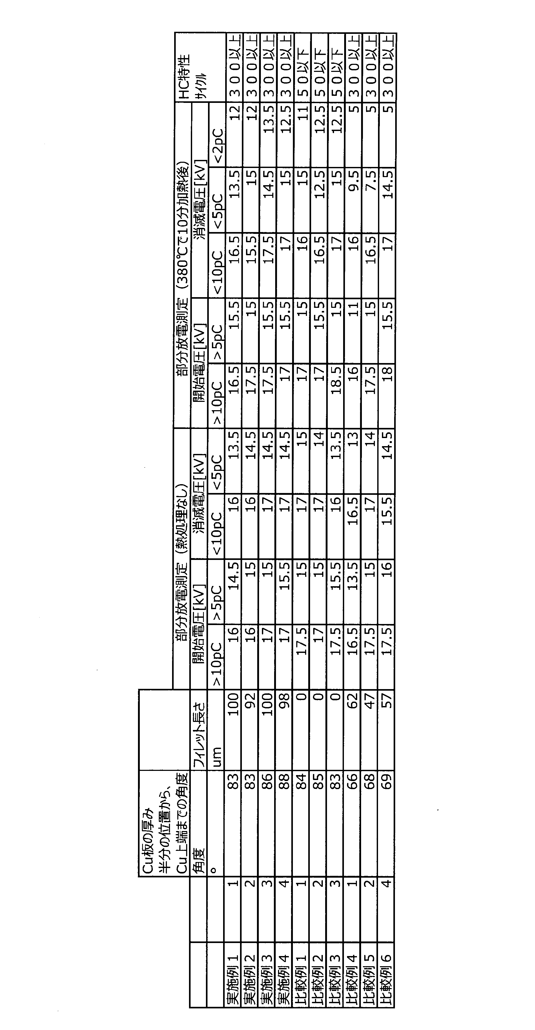
- FIG. 2 is an explanatory diagram of substrate dimensions and metal circuit board shapes (circuit pattern dimensions) of Examples 1 to 4 and Comparative Examples 1 to 6; 4 is a cross-sectional photograph showing the shape of a metal circuit board and a fillet of metal-ceramic bonding substrates of Examples 1 and 4 and Comparative Examples 2 and 5.
- FIG. 2 is an explanatory diagram of substrate dimensions and metal circuit board shapes (circuit pattern dimensions) of Examples 1 to 4 and Comparative Examples 1 to 6;
- 4 is a cross-sectional photograph showing the shape of a metal circuit board and a fillet of metal-
- a metal-ceramic bonding substrate 1 includes one or more brazing filler metal layers 11 interposed on at least one surface of a ceramic substrate 10 (for example, substantially rectangular). It has a structure in which a metal circuit board 12 is joined. In the illustrated embodiment, two (for example, substantially rectangular) metal circuit boards 12 are joined to the upper surface of a ceramic substrate 10 via a brazing material layer 11 .
- a (for example, substantially rectangular) heat radiation side metal plate 16 is joined to the lower surface of the ceramic substrate 10 via a brazing material layer 15, and a metal or composite plate called a base plate is attached to the lower surface of the heat radiation side metal plate 16.
- a heat radiating member such as a heat radiating plate made of material, metal heat radiating fins, or a cooling jacket is attached.
- the ceramic substrate 10 is preferably made of an oxide mainly composed of alumina, silica, or the like, or a non-oxide mainly composed of aluminum nitride, silicon nitride, silicon carbide, or the like, and has a length of 5 to 200 mm (preferably, Length 10 to 100 mm) x width 5 to 200 mm (preferably width 10 to 100 mm), thickness 0.25 to 3.0 mm (preferably thickness 0.3 to 1.0 mm) A substrate can be used.
- the brazing material layers 11 and 15 are preferably made of, for example, a brazing material containing an active metal, and the content of silver in (the metal component of) the brazing material is 30% by mass or more.
- the total of metal components in this active metal-containing brazing filler metal is 100% by mass, 1.0 to 7.0% by mass (preferably 1.5 to 6.5% by mass) of active metal and 30 to 95% by mass
- An active metal-containing brazing filler metal consisting of weight percent silver (preferably 50-90 weight percent, more preferably 60-80 weight percent) and the balance copper can be used. Titanium, zirconium, and hafnium can be used as active metals for this active metal-containing brazing filler metal.
- the brazing material may further contain, for example, 10% by mass or less of elements such as Sn and In.
- the metal circuit board 12 is preferably made of a metal having excellent electrical conductivity and thermal conductivity. It is preferably made of an alloy such as a copper alloy or an aluminum alloy.
- the heat radiation side metal plate 16 is preferably made of, for example, copper, a copper alloy, aluminum or an aluminum alloy in order to release heat generated from chip parts such as semiconductor elements mounted on the metal circuit board 12 .
- the surface of the metal plate 16 on the heat dissipation side (the surface opposite to the surface bonded to the ceramic substrate) is made of a material such as copper or a copper alloy (not shown), aluminum or an aluminum alloy, or an Al—SiC-based composite material.
- Radiation members such as a base plate, radiation fins, and a cooling jacket are attached by soldering, bolting, or the like.
- a protruding portion (fillet) 11a is formed so that the brazing material layer 11 protrudes outward from the lower end portion of the side surface of the metal circuit board 12. is formed.
- the protruding length (fillet length) L of the protruding portion 11a is 80 ⁇ m or more.
- the protruding length L is the protruding length of the protruding portion 11 a that protrudes outward from the lower end of the side surface of the metal circuit board 12 . More preferably, the protruding length L is 90 ⁇ m or more.
- the protruding length L is preferably 300 ⁇ m or less, more preferably 200 ⁇ m or less.
- the side surface and protruding portion 11a of the metal circuit board 12 are covered with an insulating layer 13.
- the insulating layer 13 is made of, for example, an insulating resin such as a polyimide resin.
- the side surface 12a of the metal circuit board 12 is shaped such that it gradually expands outward from the upper end (upper corner of the metal circuit board 12) 12b of the side surface of the metal circuit board 12, or is shaped like a ceramic substrate. It has a shape perpendicular to the upper surface of 10 .
- the inclination angle ⁇ of the side surface 12a of the metal circuit board 12 with respect to the upper surface of the ceramic substrate 10 is 75° or more, preferably 80° or more, preferably 100° or less, more preferably 90° or less, and there is no overhang. A shape is preferred.
- the angle of inclination ⁇ is determined by the metal circuit at the upper end (upper corner) 12b of the metal circuit board 12 and the side surface 12a of the metal circuit board 12 when the cross section of the metal-ceramic bonding substrate 1 is observed.
- a straight line (12b-P) connecting P at half the thickness of the plate 12 (half the height from the upper surface of the ceramic substrate 10 to the upper surface of the metal circuit board 12) is defined as a straight line M
- M The angle formed by M and the upper surface of the ceramic substrate 10 is assumed.
- paste-like active metal-containing brazing filler metal 20 and active metal-containing brazing filler metal 25 are applied to the upper and lower surfaces of ceramic substrate 10 by a known technique such as screen printing, spraying, or roll coating. Then, the metal plate 21 and the metal plate 26 are arranged so as to be in contact with the active metal-containing brazing filler metal 20 and the active metal-containing brazing filler metal 25, heated in a vacuum or in a non-oxidizing atmosphere, and then cooled to form a ceramic substrate. A metal plate 21 and a metal plate 26 are joined to the upper and lower surfaces of 10 .
- the active metal-containing brazing filler metal 20 may be a metal foil of a brazing filler metal having a predetermined composition, and may be arranged on the upper and lower surfaces of the ceramic substrate 10 .
- a desired circuit pattern resist 22 and a (substantially rectangular) radiation-side metal plate shape are applied to the surfaces of the metal plate 21 and the metal plate 26 bonded to the upper and lower surfaces of the ceramic substrate 10 .
- a resist 22 is applied.
- unnecessary portions of the metal plate 21 and the metal plate 26 are removed by etching with a cupric chloride etchant, iron chloride etchant, or the like. After that, as shown in FIG. 7, the resist 22 is removed.
- unnecessary portions of the active metal-containing brazing filler metal 20 and active metal-containing brazing filler metal 25 are removed. is removed with, for example, an aqueous solution containing hydrofluoric acid or an aqueous solution containing a compound that forms a complex with an active metal such as ethylenediaminetetraacetic acid (EDTA).
- EDTA ethylenediaminetetraacetic acid
- a resist 23 is applied to the metal plate 21 and the metal plate 26 over substantially the entire surface of the metal plate 21 and the metal plate 26 . It is preferable that the resist 23 has exactly the same shape as the surface of the metal plate 21 and the metal plate 26, or is applied so that the periphery of the surface (for example, about 500 ⁇ m or less) is exposed.
- the resist 23 has substantially the same shape as the metal circuit board 12 and the metal plate 16 on the heat radiation side.
- the metal circuit plate 12 and the heat radiation side metal plate 16 having a predetermined shape are formed. It is formed.
- protruding portions 11a and 15a having a predetermined protruding length (fillet length) L are formed.
- the fillet length L is controlled to a predetermined length and the inclination angle ⁇ of the side surface 12a of the metal circuit board 12 is set to 75°.
- the angle is preferably 80° or more and 100° or less, more preferably 90° or less, and the shape without overhang can be obtained.
- the resist 23 is formed on substantially the entire surface of the metal plate 21, and the fillet width L and the inclination angle ⁇ of the present invention are obtained by adjusting the etching conditions so that the fillet length L is substantially the target. be able to.
- the resist 23 is removed.
- metal plate 21 and metal plate 26, active metal-containing brazing filler metal 20 and active metal-containing brazing filler metal 25 are formed into predetermined shapes, and metal circuit board 12, heat radiation side metal plate 16, brazing layer 11 and brazing layer 15 are formed.
- the brazing material layer 11 protrudes outward from the side surface 12a of the metal circuit board 12 to form a protruding portion (fillet) 11a.
- a protruding portion (fillet) 15a in which the brazing material layer 15 protrudes from the side surface 16a of the metal plate 16 on the heat dissipation side can be formed by the same manufacturing method as that for the metal circuit plate 12. preferable.
- an insulating resin solution (insulating layer 13) is dropped so as to cover the side surface 12a of the metal circuit board 12, the protruding portion 11a of the brazing material layer 11, and the surface of the ceramic substrate 10.
- the insulating resin solution can be dropped using a resin dispenser or the like. Thereafter, the insulating resin solution is cured by heating in an inert gas atmosphere to form the insulating layer 13 .
- Polyimide resin is preferable as the insulating resin.
- the polyimide resin is diluted with a solvent such as N-methyl-2-pyrrolidone (NMP) and the viscosity at room temperature (25 ° C.) (viscosity measured with an E-type viscometer) is 50 to 1000 mPa s (preferably 70 to 900 mPa ⁇ s), and the insulating layer 13 is preferably formed by dropping the polyimide resin solution between the metal circuit boards 12 (between the circuit patterns) and around them using a resin dispenser or the like.
- NMP N-methyl-2-pyrrolidone
- a Ni plating film may be formed on the metal circuit board 12 and the protruding portion (fillet) 11a by, for example, electrolytic Ni plating or electroless Ni plating.
- a base plate (not shown) made of a metal plate or a composite material, heat dissipation fins, and a cooling jacket for water cooling can be attached to the lower surface of the heat radiation side metal plate 16 via, for example, solder or brazing material.
- the side surface 12a of the metal circuit board 12 having a predetermined angle and the protruding portion 11a of the brazing material layer 11 having a predetermined protruding width are formed.
- the insulating layer 13 By being covered with the insulating layer 13, it is possible to provide a metal-ceramic bonded substrate having good partial discharge characteristics and excellent heat cycle resistance.
- the large inclination of the side surface 12a of the metal circuit board 12 enhances the adhesion to the resin, and the protruding portion (fillet) 11a provides a stress relieving effect even after the thermal history is applied to the ceramic substrate 10. Crack generation can also be suppressed.
- two metal circuit boards 12 are joined to the upper surface of the ceramic substrate 10 via the brazing material layer 11, but the number of the metal circuit boards 12 is one. Alternatively, the number may be three or more, and it is sufficient if the metal circuit board 12 is joined to at least one surface of the ceramic substrate 10, and the heat radiation side metal plate 16 is joined to the other surface of the ceramic substrate 10. preferable.
- the metal circuit board and heat radiation side metal plate oxygen-free copper (length 20 mm, width 14 mm, thickness 0.25 mm), ceramics Substrate: Aluminum nitride (length 19.8 mm, width 13.8 mm, thickness 0.635 mm)
- Examples 1 to 4 In the same manner as in the method for producing a metal-ceramic bonded substrate described above, a paste-like active metal-containing brazing material was applied to the upper and lower surfaces of a ceramic substrate by screen printing to a thickness of 20 ⁇ m, and the active metal-containing brazing material was applied. The metal plates were placed in contact with each other, heated to 850° C. in a vacuum furnace, and then cooled to bond the metal plates to the upper and lower surfaces of the ceramic substrate.
- a circuit pattern-shaped ultraviolet curable alkali peelable resist is screened on the surface of the metal plate bonded to one side of the ceramic substrate, and the resist in the shape of the heat radiation side metal plate is screened on the surface of the metal plate bonded to the other side. It was applied by printing. After curing these resists by irradiating them with ultraviolet rays, unnecessary portions of the metal plate (copper plate) are etched with an etchant consisting of copper chloride, hydrochloric acid, and the remainder of water, and the resists are removed with an aqueous solution of sodium hydroxide. , a metal circuit board made of a copper plate and a metal plate on the heat radiation side were formed.
- the resist is applied to the entire surface of the metal circuit board and the metal plate on the heat dissipation side of the intermediate product by screen printing.
- the brazing filler metal was protruded from the portion by a predetermined length to form a protruding portion of the brazing filler metal (fillet of the brazing filler metal) to obtain a metal-ceramic bonded substrate.
- the target was a fillet length of about 100 ⁇ m.
- FIG. 13 shows substrate dimensions and metal circuit board shapes (circuit pattern dimensions) of Examples 1 to 4 and Comparative Examples 1 to 6.
- Comparative Examples 4 to 6 chemical polishing (fillet formation) was performed without forming a resist on the surface of the metal plate after removing the brazing filler metal, and the fillet length was about 50 ⁇ m. is different. In Comparative Examples 4 to 6, the thickness of the metal circuit board was reduced and the upper surface of the metal circuit board was rounded.
- FIG. 14 is a cross section of a metal-ceramic bonding substrate on which Ni—P plating is formed, which is an evaluation sample, perpendicular to the surface of the ceramic substrate and perpendicular to the sides (periphery) of the circuit pattern. Also, the partial discharge of the metal-ceramic bonded substrate was measured by the following method. First, by connecting an Al wire to the surface of each of the plurality of metal circuit boards by ultrasonic bonding, the metal circuit boards were electrically connected.
- the voltage was measured between the metal circuit board and the heat sink metal plate using a partial discharge meter (partial discharge meter DAC-PD-3 manufactured by Soken Denki Co., Ltd.). After increasing the voltage by 0.5 kV, the voltage was decreased by 0.5 kV, and the charge amount of partial discharge at the voltage was measured.
- the discharge charge amount threshold is set to 10 pC (picocoulomb) and 5 pC (picocoulomb), and the voltage generated above the discharge charge amount threshold is the initiation voltage, and the voltage below the discharge charge amount threshold is the extinction voltage.
- the metal-ceramic bonding substrate was held at -40°C for 30 minutes and then held at 150°C for 30 minutes as one cycle. evaluated.
- the heat treatment was performed by heating from room temperature to 380° C. in 10 minutes, maintaining the temperature for 10 minutes, and then returning to room temperature in 5 minutes (nitrogen 80:hydrogen 20).
- the voltage is 13 kV or more, and the partial discharge extinction voltage is 12 kV or more even when the discharge charge amount is less than 5 pC in the partial discharge measurement after heat treatment, and the partial discharge characteristics are good and the heat cycle resistance is excellent.
- a metal-ceramic bonded substrate was obtained.
Landscapes
- Engineering & Computer Science (AREA)
- Chemical & Material Sciences (AREA)
- Ceramic Engineering (AREA)
- Materials Engineering (AREA)
- Structural Engineering (AREA)
- Organic Chemistry (AREA)
- Manufacturing & Machinery (AREA)
- Microelectronics & Electronic Packaging (AREA)
- Structure Of Printed Boards (AREA)
Abstract
Description
また、このような金属-セラミックス接合基板では、接合後の熱衝撃によりセラミックス基板と金属回路板との熱膨張差により発生する熱応力により、セラミックス基板にクラックが発生し易い。
図1に示すように、本発明の実施の形態にかかる金属-セラミックス接合基板1は、(例えば略矩形の)セラミックス基板10の少なくとも一方の面にろう材層11を介して1または2以上の金属回路板12が接合された構造を有している。図示の形態では、セラミックス基板10の上面に(例えば略矩形の)2つの金属回路板12がろう材層11を介して接合されている。また、セラミックス基板10の下面には、(例えば略矩形の)放熱側金属板16がろう材層15を介して接合され、更に放熱側金属板16の下面に、ベース板とよばれる金属または複合材からなる放熱用の板材、金属製の放熱フィンや冷却ジャケットなどの(図示しない)放熱部材が取り付けられる。
なお、放熱側金属板16の表面(セラミックス基板と接合している面の反対側の面)に(図示しない)銅または銅合金、アルミニウムまたはアルミニウム合金またはAl-SiC系複合材等の材料からなるベース板や放熱フィン、冷却ジャケットなどの放熱部材が半田付けやボルト締めなどにより取付けられる。
なお、本発明において、前記傾斜角度θは、金属-セラミックス接合基板1の断面を観察したときに、金属回路板12の上端(上角部)12bと、金属回路板12の側面12aにおける金属回路板12の厚さの半分の位置(セラミックス基板10の上面から金属回路板12の上面までの高さの半分の位置)Pとを結ぶ直線(12b-P)を直線Mとしたときに、直線Mとセラミックス基板10の上面とのなす角とする。
また、傾斜角度θを測定する際には、便宜上、Pを通り図2におけるセラミックス基板10の表面に平行な直線を直線Nとしたときに、直線Mと直線Nとのなす角を測定してもよい。
次に、本発明の実施の形態にかかる金属-セラミックス接合基板1の製造方法の一例を説明する。なお、図1に示したように、セラミックス基板10の上面に2つの金属回路板12がろう材層11を介して接合された金属-セラミックス接合基板1の製造方法を例にして説明する。
なお、活性金属含有ろう材20は所定の組成のろう材の金属箔を用い、セラミックス基板10の上面および下面に配置してもよい。
なお、金属板21の不要な部分(金属板21の側面や周縁部)をエッチング除去するに際しては、はみ出し部11aのはみ出し長さ(フィレット長さ)Lが80μm以上となるようにエッチング条件(レジスト23のサイズ、エッチング液、エッチング温度や時間)を調整する。
なお同様に、セラミックス基板10の下面においても、金属回路板12と同様の製造方法で、放熱側金属板16の側面16aからろう材層15がはみ出たはみ出し部(フィレット)15aを形成することが好ましい。
なお、本発明の実施の形態の一例として、セラミックス基板10の上面に2つの金属回路板12がろう材層11を介して接合された形態を示したが、金属回路板12の個数は、1または3以上でも良く、また、セラミックス基板10の少なくとも一方の面に金属回路板12が接合されれば足り、また、セラミックス基板10の他方の面に放熱側金属板16が接合されているのが好ましい。
上述の金属-セラミックス接合基板の製造方法と同様に、セラミックス基板の上面および下面にペースト状の活性金属含有ろう材を厚さが20μmになるようにスクリーン印刷で塗布し、その活性金属含有ろう材に接触するように金属板を配置し、真空炉中で850℃に加熱した後、冷却することにより、セラミックス基板の上面および下面に金属板を接合した。
実施例1~4では、フィレット長さ100μm程度を狙いとした。
次いで、ポリイミド樹脂溶液を、樹脂用ディスペンサー(吐出圧力:0.25MPa、吐出時間:2msec、吐出間隔:0.5mm/shot)を用いて金属回路板の間(回路パターン間)とその周囲に滴下して塗布した後、250℃で30分間加熱硬化させて絶縁層を形成したものを評価サンプルとした。
実施例1~4、比較例1~6の基板寸法、金属回路板の形状(回路パターン寸法)を図13に示す。
実施例と同様に、セラミックス基板の上面および下面にペースト状の活性金属含有ろう材をスクリーン印刷で塗布し、その活性金属含有ろう材に接触するように金属板を配置し、加熱後、冷却することにより、セラミックス基板の上面および下面に金属板を接合した。その後、レジスト印刷→エッチング→レジスト除去→ろう材層除去→無電解Ni-Pめっき→ポリイミド塗布により、比較例1~3の金属-セラミックス接合基板を得た。すなわちフィレット形成(および同時に行う金属回路板の側面傾斜角制御)工程を除いて実施例と同様の製造方法にて作製し、比較例1~3ではフィレットなしとした。
実施例と同様に、セラミックス基板の上面および下面にペースト状の活性金属含有ろう材をスクリーン印刷で塗布し、その活性金属含有ろう材に接触するように金属板を配置し、加熱後、冷却することにより、セラミックス基板の上面および下面に金属板を接合した。その後、レジスト印刷→エッチング→レジスト除去→ろう材層除去→化学研磨→無電解Niめっき→ポリイミド塗布により、比較例4~6の金属-セラミックス接合基板を得た。比較例4~6では、実施例と比べてろう材除去後に金属板の表面にレジストを形成せずに化学研磨(フィレット形成)を行っていること、またフィレット長さ50μm程度を狙いとした工程が異なる。比較例4~6では、金属回路板の厚さが薄くなり、金属回路板の上面が丸くなった。
また、金属-セラミックス接合基板の部分放電を次の方法で測定した。まず、複数ある各金属回路板の表面にAlワイヤーを超音波ボンディングで接続することにより、各金属回路板の間を電気的に接続した。次いで金属-セラミックス接合基板を絶縁油中に浸漬した状態で、金属回路板と放熱金属板の間に電圧を部分放電測定器(総研電気株式会社製の部分放電測定器DAC-PD-3)を用いて0.5kVずつ昇圧した後、0.5kVずつ降圧し、その電圧における部分放電の電荷量の測定を実施した。放電電荷量の閾値を10pC(ピコクーロン)および5pC(ピコクーロン)に設定し、それぞれの放電電荷量の閾値より大きく発生した電圧を開始電圧、それぞれの放電電荷量の閾値未満となった電圧を消滅電圧として記録した。
また、金属-セラミックス接合基板を-40℃で30分保持、150℃で30分保持を1サイクルとして、50サイクルごとに室温に戻してセラミックスのクラック発生有無を確認することにより、耐ヒートサイクル性を評価した。
フィレットがない比較例1~3の評価サンプルは部分放電特性が良好であり、380℃で熱処理後も部分放電特性が維持されるが、ヒートサイクル50サイクル後にセラミックス基板にクラックが発生しており耐ヒートサイクル(HC)特性に劣る。なお、熱処理は、室温から10分間で380℃まで昇温させて10分間保持した後に5分間で室温に戻す通炉処理(窒素80:水素20)を行った。
金属回路板の側面(Cu側面)の角度が75°以下でフィレットの長さが70μm以下の比較例4~6は、熱処理後の部分放電消滅電圧が10kV以下になることがあり、部分放電特性に劣ることが判明した。
一方、断面において金属回路板の側面(Cu板側面)の角度が80°以上で、フィレットが90μmを超えている実施例1~4は、熱処理前のポリイミド塗布後の部分放電開始および部分放電消滅電圧が13kV以上であり、熱処理実施後の部分放電測定に置いて放電電荷量5pC未満の条件の場合でも部分放電消滅電圧が、12kV以上となり、部分放電特性が良好で且つ耐ヒートサイクル性に優れた金属-セラミックス接合基板を得ることができた。
10 セラミックス基板
11 ろう材層
11a はみ出し部(フィレット)
12 金属回路板
12a 側面
12b 上端(上角部)
13 絶縁層
15 ろう材層
15a はみ出し部(フィレット)
16 放熱側金属板
20 活性金属含有ろう材
21 金属板
22、23 レジスト
Claims (14)
- セラミックス基板の一方の面にろう材層を介して金属回路板が接合された金属-セラミックス接合基板であって、
前記金属回路板の側面の下端部から外側に80μm以上はみ出した前記ろう材層のはみ出し部が形成され、
前記金属回路板の側面が前記セラミックス基板の表面に対して75°以上の傾斜角度を有し、
前記金属回路板の側面および前記ろう材層のはみ出し部が絶縁層で覆われている、金属-セラミックス接合基板。 - 前記セラミックス基板の他方の面に放熱側金属板が接合されていることを特徴とする、請求項1に記載の金属-セラミックス接合基板。
- 前記放熱側金属板が銅または銅合金であることを特徴とする、請求項2に記載の金属-セラミックス接合基板。
- 前記金属回路板が銅または銅合金であることを特徴とする、請求項1~3のいずれかに記載の金属-セラミックス接合基板。
- 前記金属回路板と前記ろう材層のはみ出し部の表面にニッケルめっきまたはニッケル合金めっきが形成されていることを特徴とする、請求項1~4のいずれかに記載の金属-セラミックス接合基板。
- 前記絶縁層が樹脂であることを特徴とする、請求項1~5のいずれかに記載の金属-セラミックス接合基板。
- 前記樹脂がポリイミド樹脂を主成分とすることを特徴とする、請求項6に記載の金属-セラミックス接合基板。
- セラミックス基板の一方の面にろう材層を介して金属板が接合された金属-セラミックス接合体において、前記金属板の不要な部分を除去して金属回路板を形成し、前記金属回路板の側面の下端部から前記ろう材層を80μm以上はみ出させて前記ろう材層のはみ出し部を形成するとともに、前記金属回路板の側面がセラミックス基板の表面に対して75°以上の傾斜角度となるように、金属回路板の側面をエッチングした後、
前記金属回路板の側面と前記ろう材層のはみ出し部を覆うように絶縁層を形成する、金属-セラミックス接合基板の製造方法。 - セラミックス基板の一方の面にろう材層を介して金属板が接合されるとともに、他方の面に放熱側ろう材層を介して金属板が接合された金属-セラミックス接合体において、一方の面の前記金属板および他方の面の前記金属板の不要な部分を除去し、前記セラミックス基板の一方の面に金属回路板を形成するとともに、他方の面に放熱側金属板を形成することを特徴とする、請求項8に記載の金属-セラミックス接合基板の製造方法。
- 前記放熱側金属板が銅または銅合金であることを特徴とする、請求項9に記載の金属-セラミックス接合基板の製造方法。
- 前記金属回路板が銅または銅合金であることを特徴とする、請求項8~10のいずれかに記載の金属-セラミックス接合基板の製造方法。
- 前記金属回路板および前記ろう材層のはみ出し部の表面にニッケルまたはニッケル合金めっきを形成することを特徴とする、請求項8~11のいずれかに記載の金属-セラミックス接合基板の製造方法。
- 絶縁性の樹脂からなるコーティング材を塗布した後、硬化させることにより、前記絶縁層を形成することを特徴とする、請求項8~12のいずれかに記載の金属-セラミックス接合基板の製造方法。
- 前記樹脂がポリイミド樹脂を主成分とすることを特徴とする、請求項13に記載の金属-セラミックス接合基板の製造方法。
Priority Applications (3)
| Application Number | Priority Date | Filing Date | Title |
|---|---|---|---|
| CN202280063359.6A CN117981073A (zh) | 2021-09-21 | 2022-07-11 | 金属-陶瓷接合基板及其制造方法 |
| US18/682,670 US20240395679A1 (en) | 2021-09-21 | 2022-07-11 | Metal-ceramic bonded substrate and manufacturing method thereof |
| EP22872521.4A EP4407672A4 (en) | 2021-09-21 | 2022-07-11 | METAL-CERAMIC JOINT SUBSTRATE AND METHOD FOR PRODUCING SAME |
Applications Claiming Priority (2)
| Application Number | Priority Date | Filing Date | Title |
|---|---|---|---|
| JP2021153278A JP7739105B2 (ja) | 2021-09-21 | 2021-09-21 | 金属-セラミックス接合基板およびその製造方法 |
| JP2021-153278 | 2021-09-21 |
Publications (1)
| Publication Number | Publication Date |
|---|---|
| WO2023047765A1 true WO2023047765A1 (ja) | 2023-03-30 |
Family
ID=85720447
Family Applications (1)
| Application Number | Title | Priority Date | Filing Date |
|---|---|---|---|
| PCT/JP2022/027275 Ceased WO2023047765A1 (ja) | 2021-09-21 | 2022-07-11 | 金属-セラミックス接合基板およびその製造方法 |
Country Status (5)
| Country | Link |
|---|---|
| US (1) | US20240395679A1 (ja) |
| EP (1) | EP4407672A4 (ja) |
| JP (1) | JP7739105B2 (ja) |
| CN (1) | CN117981073A (ja) |
| WO (1) | WO2023047765A1 (ja) |
Families Citing this family (3)
| Publication number | Priority date | Publication date | Assignee | Title |
|---|---|---|---|---|
| WO2022210507A1 (ja) * | 2021-03-30 | 2022-10-06 | 株式会社 東芝 | セラミックス回路基板の製造方法 |
| CN121219095A (zh) * | 2023-05-24 | 2025-12-26 | 三菱电机株式会社 | 接合方法、半导体装置的制造方法和半导体装置 |
| EP4563550A1 (de) | 2023-11-30 | 2025-06-04 | Heraeus Electronics GmbH & Co. KG | Verfahren zur strukturierung eines metall-keramik-verbunds |
Citations (5)
| Publication number | Priority date | Publication date | Assignee | Title |
|---|---|---|---|---|
| JP2002076190A (ja) | 2000-08-24 | 2002-03-15 | Toshiba Corp | 回路基板、半導体装置及びこれらの製造方法 |
| JP2004311691A (ja) * | 2003-04-07 | 2004-11-04 | Hitachi Metals Ltd | 回路用金属板およびセラミックス回路基板 |
| JP2005116602A (ja) | 2003-10-03 | 2005-04-28 | Denki Kagaku Kogyo Kk | 回路基板及びその製造方法 |
| JP2006228918A (ja) * | 2005-02-17 | 2006-08-31 | Hitachi Metals Ltd | セラミックス回路基板およびそれを用いた半導体モジュール |
| JP2016051778A (ja) * | 2014-08-29 | 2016-04-11 | Dowaメタルテック株式会社 | 金属−セラミックス接合基板 |
Family Cites Families (14)
| Publication number | Priority date | Publication date | Assignee | Title |
|---|---|---|---|---|
| US6936337B2 (en) * | 2001-09-28 | 2005-08-30 | Dowa Mining Co., Ltd. | Metal/ceramic circuit board |
| JP3648189B2 (ja) * | 2001-09-28 | 2005-05-18 | 同和鉱業株式会社 | 金属−セラミックス回路基板 |
| JP6262968B2 (ja) * | 2013-09-09 | 2018-01-17 | Dowaメタルテック株式会社 | 電子部品搭載基板およびその製造方法 |
| JP6829204B2 (ja) * | 2015-09-28 | 2021-02-10 | 株式会社東芝 | 窒化珪素回路基板およびそれを用いた半導体モジュール |
| EP3358614B1 (en) * | 2015-09-28 | 2022-12-14 | Kabushiki Kaisha Toshiba | Circuit substrate and semiconductor device |
| DE112018000457T5 (de) * | 2017-02-23 | 2019-09-26 | Ngk Insulators, Ltd. | Isoliertes wärmeableitungssubstrat |
| JP6799479B2 (ja) * | 2017-03-03 | 2020-12-16 | Dowaメタルテック株式会社 | 金属−セラミックス回路基板の製造方法 |
| JP7002993B2 (ja) * | 2018-05-10 | 2022-01-20 | 株式会社 日立パワーデバイス | パワー半導体モジュール |
| WO2019221174A1 (ja) * | 2018-05-16 | 2019-11-21 | 株式会社 東芝 | セラミックス銅回路基板およびその製造方法 |
| EP3860317B1 (en) * | 2018-09-27 | 2024-07-24 | Denka Company Limited | Bonded substrate, metal circuit board, and circuit board |
| JP7537900B2 (ja) * | 2020-03-31 | 2024-08-21 | Dowaメタルテック株式会社 | ろう材およびその製造方法並びに金属-セラミックス接合基板の製造方法 |
| JP7587364B2 (ja) * | 2020-07-15 | 2024-11-20 | Dowaメタルテック株式会社 | 絶縁基板およびその製造方法 |
| CN116830813A (zh) * | 2021-02-17 | 2023-09-29 | 株式会社东芝 | 陶瓷电路基板及采用其的半导体装置 |
| JP7666202B2 (ja) * | 2021-07-30 | 2025-04-22 | 三菱マテリアル株式会社 | 銅/セラミックス接合体、および、絶縁回路基板 |
-
2021
- 2021-09-21 JP JP2021153278A patent/JP7739105B2/ja active Active
-
2022
- 2022-07-11 CN CN202280063359.6A patent/CN117981073A/zh active Pending
- 2022-07-11 US US18/682,670 patent/US20240395679A1/en active Pending
- 2022-07-11 WO PCT/JP2022/027275 patent/WO2023047765A1/ja not_active Ceased
- 2022-07-11 EP EP22872521.4A patent/EP4407672A4/en active Pending
Patent Citations (5)
| Publication number | Priority date | Publication date | Assignee | Title |
|---|---|---|---|---|
| JP2002076190A (ja) | 2000-08-24 | 2002-03-15 | Toshiba Corp | 回路基板、半導体装置及びこれらの製造方法 |
| JP2004311691A (ja) * | 2003-04-07 | 2004-11-04 | Hitachi Metals Ltd | 回路用金属板およびセラミックス回路基板 |
| JP2005116602A (ja) | 2003-10-03 | 2005-04-28 | Denki Kagaku Kogyo Kk | 回路基板及びその製造方法 |
| JP2006228918A (ja) * | 2005-02-17 | 2006-08-31 | Hitachi Metals Ltd | セラミックス回路基板およびそれを用いた半導体モジュール |
| JP2016051778A (ja) * | 2014-08-29 | 2016-04-11 | Dowaメタルテック株式会社 | 金属−セラミックス接合基板 |
Non-Patent Citations (1)
| Title |
|---|
| See also references of EP4407672A4 |
Also Published As
| Publication number | Publication date |
|---|---|
| JP7739105B2 (ja) | 2025-09-16 |
| US20240395679A1 (en) | 2024-11-28 |
| CN117981073A (zh) | 2024-05-03 |
| EP4407672A4 (en) | 2025-04-09 |
| JP2023045082A (ja) | 2023-04-03 |
| EP4407672A1 (en) | 2024-07-31 |
Similar Documents
| Publication | Publication Date | Title |
|---|---|---|
| JP4015023B2 (ja) | 電子回路用部材及びその製造方法並びに電子部品 | |
| US10937715B2 (en) | Substrate for power module, collective substrate for power modules, and method for manufacturing substrate for power module | |
| US10872841B2 (en) | Ceramic metal circuit board and semiconductor device using the same | |
| CN108541149B (zh) | 金属/陶瓷电路板的制造方法 | |
| WO2023047765A1 (ja) | 金属-セラミックス接合基板およびその製造方法 | |
| JP5128951B2 (ja) | ヒートシンクモジュール及びその製造方法 | |
| TWI713746B (zh) | 功率模組用基板 | |
| JP2002043482A (ja) | 電子回路用部材及びその製造方法並びに電子部品 | |
| JP2010238753A (ja) | 放熱用部材およびこれを用いたモジュール | |
| JP6904094B2 (ja) | 絶縁回路基板の製造方法 | |
| JP5069485B2 (ja) | 金属ベース回路基板 | |
| JP2004172182A (ja) | 回路基板及びその製造方法 | |
| JP7792033B2 (ja) | セラミックス回路基板の製造方法および半導体装置の製造方法 | |
| JP2017065935A (ja) | セラミックス回路基板 | |
| JP5902557B2 (ja) | 多層配線基板および電子装置 | |
| JP2004055576A (ja) | 回路基板及びそれを用いたパワーモジュール | |
| JP7299672B2 (ja) | セラミックス回路基板及びその製造方法 | |
| JPH10167804A (ja) | セラミックス基板及びそれを用いた回路基板とその製造方法 | |
| JP6621353B2 (ja) | 耐熱性セラミックス回路基板 | |
| JP2001135902A (ja) | セラミックス回路基板 | |
| JP2000058723A (ja) | 回路基板 | |
| JPH10224059A (ja) | ヒートシンク | |
| JP4282627B2 (ja) | セラミックス回路基板、その製造方法およびそれを用いた電力制御部品。 | |
| JP3526711B2 (ja) | 窒化アルミニウム回路基板 | |
| JP3812988B2 (ja) | 回路基板 |
Legal Events
| Date | Code | Title | Description |
|---|---|---|---|
| 121 | Ep: the epo has been informed by wipo that ep was designated in this application |
Ref document number: 22872521 Country of ref document: EP Kind code of ref document: A1 |
|
| WWE | Wipo information: entry into national phase |
Ref document number: 18682670 Country of ref document: US |
|
| WWE | Wipo information: entry into national phase |
Ref document number: 202280063359.6 Country of ref document: CN |
|
| WWE | Wipo information: entry into national phase |
Ref document number: 2022872521 Country of ref document: EP |
|
| NENP | Non-entry into the national phase |
Ref country code: DE |
|
| ENP | Entry into the national phase |
Ref document number: 2022872521 Country of ref document: EP Effective date: 20240422 |