WO2023053503A1 - 撮像装置、電子機器および撮像装置の製造方法 - Google Patents
撮像装置、電子機器および撮像装置の製造方法 Download PDFInfo
- Publication number
- WO2023053503A1 WO2023053503A1 PCT/JP2022/011295 JP2022011295W WO2023053503A1 WO 2023053503 A1 WO2023053503 A1 WO 2023053503A1 JP 2022011295 W JP2022011295 W JP 2022011295W WO 2023053503 A1 WO2023053503 A1 WO 2023053503A1
- Authority
- WO
- WIPO (PCT)
- Prior art keywords
- layer
- rewiring layer
- imaging device
- sealing resin
- image sensor
- Prior art date
- Legal status (The legal status is an assumption and is not a legal conclusion. Google has not performed a legal analysis and makes no representation as to the accuracy of the status listed.)
- Ceased
Links
Images


Classifications
-
- H—ELECTRICITY
- H10—SEMICONDUCTOR DEVICES; ELECTRIC SOLID-STATE DEVICES NOT OTHERWISE PROVIDED FOR
- H10F—INORGANIC SEMICONDUCTOR DEVICES SENSITIVE TO INFRARED RADIATION, LIGHT, ELECTROMAGNETIC RADIATION OF SHORTER WAVELENGTH OR CORPUSCULAR RADIATION
- H10F39/00—Integrated devices, or assemblies of multiple devices, comprising at least one element covered by group H10F30/00, e.g. radiation detectors comprising photodiode arrays
- H10F39/011—Manufacture or treatment of image sensors covered by group H10F39/12
- H10F39/026—Wafer-level processing
-
- H—ELECTRICITY
- H10—SEMICONDUCTOR DEVICES; ELECTRIC SOLID-STATE DEVICES NOT OTHERWISE PROVIDED FOR
- H10F—INORGANIC SEMICONDUCTOR DEVICES SENSITIVE TO INFRARED RADIATION, LIGHT, ELECTROMAGNETIC RADIATION OF SHORTER WAVELENGTH OR CORPUSCULAR RADIATION
- H10F39/00—Integrated devices, or assemblies of multiple devices, comprising at least one element covered by group H10F30/00, e.g. radiation detectors comprising photodiode arrays
- H10F39/80—Constructional details of image sensors
- H10F39/811—Interconnections
-
- H—ELECTRICITY
- H10—SEMICONDUCTOR DEVICES; ELECTRIC SOLID-STATE DEVICES NOT OTHERWISE PROVIDED FOR
- H10F—INORGANIC SEMICONDUCTOR DEVICES SENSITIVE TO INFRARED RADIATION, LIGHT, ELECTROMAGNETIC RADIATION OF SHORTER WAVELENGTH OR CORPUSCULAR RADIATION
- H10F39/00—Integrated devices, or assemblies of multiple devices, comprising at least one element covered by group H10F30/00, e.g. radiation detectors comprising photodiode arrays
- H10F39/011—Manufacture or treatment of image sensors covered by group H10F39/12
- H10F39/014—Manufacture or treatment of image sensors covered by group H10F39/12 of CMOS image sensors
-
- H—ELECTRICITY
- H10—SEMICONDUCTOR DEVICES; ELECTRIC SOLID-STATE DEVICES NOT OTHERWISE PROVIDED FOR
- H10F—INORGANIC SEMICONDUCTOR DEVICES SENSITIVE TO INFRARED RADIATION, LIGHT, ELECTROMAGNETIC RADIATION OF SHORTER WAVELENGTH OR CORPUSCULAR RADIATION
- H10F39/00—Integrated devices, or assemblies of multiple devices, comprising at least one element covered by group H10F30/00, e.g. radiation detectors comprising photodiode arrays
- H10F39/011—Manufacture or treatment of image sensors covered by group H10F39/12
- H10F39/024—Manufacture or treatment of image sensors covered by group H10F39/12 of coatings or optical elements
-
- H—ELECTRICITY
- H10—SEMICONDUCTOR DEVICES; ELECTRIC SOLID-STATE DEVICES NOT OTHERWISE PROVIDED FOR
- H10F—INORGANIC SEMICONDUCTOR DEVICES SENSITIVE TO INFRARED RADIATION, LIGHT, ELECTROMAGNETIC RADIATION OF SHORTER WAVELENGTH OR CORPUSCULAR RADIATION
- H10F39/00—Integrated devices, or assemblies of multiple devices, comprising at least one element covered by group H10F30/00, e.g. radiation detectors comprising photodiode arrays
- H10F39/011—Manufacture or treatment of image sensors covered by group H10F39/12
- H10F39/028—Manufacture or treatment of image sensors covered by group H10F39/12 performed after manufacture of the image sensors, e.g. annealing, gettering of impurities, short-circuit elimination or recrystallisation
-
- H—ELECTRICITY
- H10—SEMICONDUCTOR DEVICES; ELECTRIC SOLID-STATE DEVICES NOT OTHERWISE PROVIDED FOR
- H10F—INORGANIC SEMICONDUCTOR DEVICES SENSITIVE TO INFRARED RADIATION, LIGHT, ELECTROMAGNETIC RADIATION OF SHORTER WAVELENGTH OR CORPUSCULAR RADIATION
- H10F39/00—Integrated devices, or assemblies of multiple devices, comprising at least one element covered by group H10F30/00, e.g. radiation detectors comprising photodiode arrays
- H10F39/80—Constructional details of image sensors
- H10F39/804—Containers or encapsulations
-
- H—ELECTRICITY
- H10—SEMICONDUCTOR DEVICES; ELECTRIC SOLID-STATE DEVICES NOT OTHERWISE PROVIDED FOR
- H10F—INORGANIC SEMICONDUCTOR DEVICES SENSITIVE TO INFRARED RADIATION, LIGHT, ELECTROMAGNETIC RADIATION OF SHORTER WAVELENGTH OR CORPUSCULAR RADIATION
- H10F39/00—Integrated devices, or assemblies of multiple devices, comprising at least one element covered by group H10F30/00, e.g. radiation detectors comprising photodiode arrays
- H10F39/80—Constructional details of image sensors
- H10F39/805—Coatings
-
- H—ELECTRICITY
- H10—SEMICONDUCTOR DEVICES; ELECTRIC SOLID-STATE DEVICES NOT OTHERWISE PROVIDED FOR
- H10W—GENERIC PACKAGES, INTERCONNECTIONS, CONNECTORS OR OTHER CONSTRUCTIONAL DETAILS OF DEVICES COVERED BY CLASS H10
- H10W70/00—Package substrates; Interposers; Redistribution layers [RDL]
- H10W70/60—Insulating or insulated package substrates; Interposers; Redistribution layers
- H10W70/62—Insulating or insulated package substrates; Interposers; Redistribution layers characterised by their interconnections
- H10W70/65—Shapes or dispositions of interconnections
- H10W70/652—Cross-sectional shapes
-
- H—ELECTRICITY
- H10—SEMICONDUCTOR DEVICES; ELECTRIC SOLID-STATE DEVICES NOT OTHERWISE PROVIDED FOR
- H10W—GENERIC PACKAGES, INTERCONNECTIONS, CONNECTORS OR OTHER CONSTRUCTIONAL DETAILS OF DEVICES COVERED BY CLASS H10
- H10W72/00—Interconnections or connectors in packages
- H10W72/20—Bump connectors, e.g. solder bumps or copper pillars; Dummy bumps; Thermal bumps
-
- H—ELECTRICITY
- H10—SEMICONDUCTOR DEVICES; ELECTRIC SOLID-STATE DEVICES NOT OTHERWISE PROVIDED FOR
- H10W—GENERIC PACKAGES, INTERCONNECTIONS, CONNECTORS OR OTHER CONSTRUCTIONAL DETAILS OF DEVICES COVERED BY CLASS H10
- H10W72/00—Interconnections or connectors in packages
- H10W72/90—Bond pads, in general
-
- H—ELECTRICITY
- H10—SEMICONDUCTOR DEVICES; ELECTRIC SOLID-STATE DEVICES NOT OTHERWISE PROVIDED FOR
- H10W—GENERIC PACKAGES, INTERCONNECTIONS, CONNECTORS OR OTHER CONSTRUCTIONAL DETAILS OF DEVICES COVERED BY CLASS H10
- H10W74/00—Encapsulations, e.g. protective coatings
- H10W74/10—Encapsulations, e.g. protective coatings characterised by their shape or disposition
- H10W74/15—Encapsulations, e.g. protective coatings characterised by their shape or disposition on active surfaces of flip-chip devices, e.g. underfills
-
- H—ELECTRICITY
- H10—SEMICONDUCTOR DEVICES; ELECTRIC SOLID-STATE DEVICES NOT OTHERWISE PROVIDED FOR
- H10W—GENERIC PACKAGES, INTERCONNECTIONS, CONNECTORS OR OTHER CONSTRUCTIONAL DETAILS OF DEVICES COVERED BY CLASS H10
- H10W90/00—Package configurations
- H10W90/701—Package configurations characterised by the relative positions of pads or connectors relative to package parts
- H10W90/721—Package configurations characterised by the relative positions of pads or connectors relative to package parts of bump connectors
- H10W90/724—Package configurations characterised by the relative positions of pads or connectors relative to package parts of bump connectors between a chip and a stacked insulating package substrate, interposer or RDL
Definitions
- the present disclosure relates to an imaging device, an electronic device, and a method for manufacturing an imaging device.
- an imaging device including an imaging device such as a CMOS image sensor installed in an electronic device such as a smartphone, for example, there is the following configuration. That is, for example, a circuit board such as a ceramic substrate or a printed circuit board (hereinafter simply referred to as "substrate”) is used as an object for mounting the imaging element, and the imaging element and the substrate are electrically connected by wire bonding. .
- a circuit board such as a ceramic substrate or a printed circuit board (hereinafter simply referred to as "substrate”) is used as an object for mounting the imaging element, and the imaging element and the substrate are electrically connected by wire bonding. .
- connection pins of the imaging device In recent years, in imaging devices, the number of connection pins of the imaging device has increased, while the pitch of the connection pins has been narrowed due to the demand for smaller package structures for imaging devices, making it difficult to connect by wire bonding. It has become. In addition, in the package structure of the imaging device, there is a demand for a low profile (minimization in the height direction). , there is a limit to low profile.
- the imaging element mounted in the cavity of the substrate is likely to tilt with respect to the substrate.
- the external connection terminal is provided on the back side of a substrate on which an imaging device is mounted, and the external connection terminal is electrically connected to a base substrate on which the imaging device is mounted by means of solder bumps, the solder is melted.
- the imaging device will be tilted with respect to the base substrate due to the reflow process for reflowing.
- the use of a substrate with cavities causes an increase in cost compared to a normal substrate without cavities.
- Patent Document 2 discloses a configuration in which a mold portion as a sealing resin portion is formed in the periphery of an image pickup device excluding a pixel forming surface of the image pickup device, and a rewiring layer is provided on the peripheral region of the image pickup device and the mold portion. is disclosed.
- the rewiring layer is formed so as to be directly connected to the pads provided in the peripheral region of the imaging device. According to such a configuration, in the manufacturing process of the imaging device, the rewiring layer is formed for the configuration in which the sealing resin portion is formed around the imaging element. Therefore, in the process of forming the rewiring layer, it is necessary to protect the pixel forming surface of the imaging element from the chemical solution and the like used for forming the rewiring layer.
- the protective film In order to protect the pixel formation surface of the imaging element, for example, it is conceivable to form a protective film on the pixel formation surface. However, when such a method is adopted, if the removal of the protective film once formed is insufficient, or if a method of leaving the protective film is adopted, the protective film existing on the pixel formation surface will not transmit light. properties and the refractive index of light, etc., and may interfere with the function of the imaging device.
- An object of the present technology is to provide an imaging device, an electronic device, and a method for manufacturing an imaging device that can reduce the size and height of the device without impairing the imaging performance of the imaging element.
- An imaging device includes an imaging device having, on a surface side, a pixel region in which a large number of pixels are formed and a peripheral region that is a region surrounding the pixel region; A rewiring layer having openings penetrating through a region including the pixel region, and a sealing resin material formed to cover the periphery of the imaging element and the rear surface side of the rewiring layer. and a connecting portion provided on the peripheral region of the imaging element and electrically connecting the imaging element and the rewiring layer.
- the imaging device wherein the rewiring layer has a peripheral region covering portion that covers at least part of the peripheral region of the imaging element in plan view, and the connection portion is provided between the imaging element and the peripheral area covering portion.
- imaging device Another aspect of the imaging device according to the present technology is the imaging device, wherein the imaging element is positioned within a recess formed in the sealing resin portion and provided within a layer thickness range of the sealing resin portion. It is what is done.
- the imaging device further includes an underfill section formed of a material different from the sealing resin material and covering the connection section.
- the imaging device has a stepped surface forming a step on a lower side with respect to the pixel region in the peripheral region, and the connection section includes: It is provided on the step surface.
- the rewiring layer gradually increases the opening area of the opening from the front surface side to the back surface side of the rewiring layer. It is made into the inclined surface inclined so that it may spread out.
- a layout space of the connection section and the A partition is provided to partition the space on the pixel region side.
- a It further comprises a second rewiring layer.
- An electronic device includes an image sensor having a pixel region in which a large number of pixels are formed and a peripheral region, which is a region surrounding the pixel region, on the surface side, and provided on the surface side of the image sensor, A rewiring layer having openings penetrating through a region including the pixel region, and a sealing resin material formed to cover the periphery of the imaging element and the rear surface side of the rewiring layer. and a connecting portion provided on the peripheral region of the imaging element and electrically connecting the imaging element and the rewiring layer.
- a method for manufacturing an imaging device includes steps of preparing a supporting member having a peeling layer on one surface of a supporting substrate; a step of forming a layer, and covering the opening with an imaging element on the rewiring layer so that the surface side of the imaging element faces the peeling layer side, and electrically connecting the imaging element to the rewiring layer. forming a sealing resin portion with a sealing resin material so as to cover the side opposite to the release layer side of the rewiring layer and the periphery of the imaging element; and peeling the supporting substrate from the rewiring layer.
- the sealing resin portion is formed on the side opposite to the rewiring layer side. It has a step of thinning from.
- the sealing resin is added after the step of providing the imaging element and before the step of forming the sealing resin portion. It has a step of forming an underfill portion covering the connection portion with a material different from the material.
- the wall surface forming the opening is shifted from the release layer side to the release layer side.
- the rewiring layer is formed so as to form an inclined surface that is inclined so as to gradually widen the opening area of the opening toward the opposite side.
- the imaging device in the method for manufacturing an imaging device, after the step of forming the sealing resin portion, the imaging device is mounted on the imaging device and the sealing resin portion. forming a second rewiring layer electrically connected to the rewiring layer on the rear surface side of the second rewiring layer.
- FIG. 1 is a block diagram showing a configuration example of an electronic device including a solid-state imaging device according to an embodiment of the present technology
- the present technology integrates the imaging device and the rewiring layer by means of a sealing resin portion made of a sealing resin material. It is intended to reduce the size and height of the device while ensuring the imaging performance of the device.
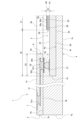
- FIG. 1 A configuration example of a solid-state imaging device 1 according to a first embodiment of the present technology will be described with reference to FIGS. 1 to 4.
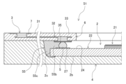
- the solid-state imaging device 1 includes an image sensor 2 as a solid-state imaging element, a rewiring layer 3, a sealing resin portion 4, and metal bumps 5 as connecting portions.
- the solid-state imaging device 1 has a substantially rectangular plate-like outer shape, and has a front surface portion 1a and a rear surface portion 1b, both of which are horizontal surface portions, and four side portions.
- the solid-state imaging device 1 has a lower layer portion mainly composed of the sealing resin portion 4 and an upper layer portion composed of the rewiring layer 3 . It is provided in an embedded manner.
- the image sensor 2 has a light-receiving surface on the upper side, and the rewiring layer 3 is formed with a wiring layer opening 6 that is an opening for securing a passage of light received by the image sensor 2 .
- the solid-state imaging device 1 has a package structure in which the image sensor 2 and the rewiring layer 3 are integrated by a sealing resin portion 4, which is a mold resin portion, and the rewiring layer 3 extends outside the outline of the image sensor 2. It has a so-called FOWLP (Fan Out Wafer Level Package) structure.
- a plurality of external connection terminals 7 are formed on the edge of the surface portion 1a.
- the external connection terminal 7 is an electrode portion formed in a state of being exposed on the surface portion 1a as a part of the rewiring that constitutes the rewiring layer 3 .
- the image sensor 2 is provided at a position biased to one side (right side in FIG. 2) of the longitudinal direction of the solid-state imaging device 1 in plan view (horizontal direction in FIG. 2).
- a plurality of external connection terminals 7 are provided at the end portion on the other side in the longitudinal direction of the solid-state imaging device 1 (the left side in FIG. 2).
- one end side of a flexible substrate 8 called FPC (Flexible Printed Circuits) or the like is electrically connected to the external connection terminal 7 by a connection portion 9 formed by solder plating or the like. Connected.
- a connector is provided on the other end side of the flexible board 8, and the other end side of the flexible board 8 is connected to a predetermined external device.
- the solid-state imaging device 1 receives the mounting of the lens unit 10 on the surface portion 1a side.
- the lens unit 10 forms an image of light from a subject on the image sensor 2 using a plurality of lenses 11 .
- the lens unit 10 has a tubular support cylinder 12 , and supports a plurality of lenses 11 inside the support cylinder 12 .
- the support cylinder 12 has its cylinder axis aligned with the optical axis of the lens unit 10, and supports three lenses 11 in a vertically stacked state via spacers or the like. ing.
- the optical axis of the lens unit 10 is a vertical straight line passing through the centers of the three lenses 11 . Note that the number of lenses 11 is not particularly limited.
- the lens unit 10 is mounted on the solid-state imaging device 1 with the mounting surface 13 on the lower side of the support cylinder 12 fixed on the surface portion 1a of the solid-state imaging device 1 with an adhesive or the like.
- the lens unit 10 is provided on the solid-state imaging device 1 , light collected by the plurality of lenses 11 enters the light receiving surface of the image sensor 2 .
- Each configuration included in the solid-state imaging device 1 will be described below.
- the image sensor 2 is electrically connected to the rewiring layer 3.
- the image sensor 2 is a semiconductor element including a semiconductor substrate made of silicon (Si), which is an example of a semiconductor. As shown in FIG. 2, the image sensor 2 is a rectangular plate-shaped chip, and the front surface 2a, which is the upper plate surface, is the light receiving surface side, and the opposite plate surface is the back surface 2b.
- the image sensor 2 also has four side portions 2c formed perpendicular to the plate surface.
- the image sensor 2 has a plate thickness thinner than the layer thickness of the sealing resin portion 4, and is embedded in the sealing resin portion 4 while exposing the surface 2a side.
- the image sensor 2 has an external dimension in plan view larger than the opening dimension of the wiring layer opening 6 , and has a peripheral edge positioned below the opening edge of the wiring layer opening 6 of the rewiring layer 3 .
- a plurality of light receiving elements are formed on the surface 2a side of the image sensor 2 .
- the image sensor 2 is a CMOS (Complementary Metal Oxide Semiconductor) type image sensor.
- the image sensor 2 may be another imaging element such as a CCD (Charge Coupled Device) type image sensor.
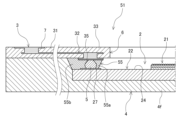
- the image sensor 2 has a pixel region 21, which is a light receiving region in which a large number of pixels 23 are formed, and a peripheral region 22, which is a region around the pixel region 21, on the surface 2a side. have.
- a large number of pixels 23 are arranged in a predetermined arrangement such as a Bayer arrangement, and constitute a light receiving portion of the image sensor 2 .
- a predetermined peripheral circuit is formed in the peripheral region 22 .
- the pixel region 21 includes an effective pixel region in which signal charges are generated, amplified, and read out by photoelectric conversion in each pixel 23 .
- a pixel 23 in the pixel region 21 has a photodiode as a photoelectric conversion unit having a photoelectric conversion function and a plurality of pixel transistors.
- a photodiode is formed on a semiconductor substrate 20 .
- the pad electrode 27 becomes a portion electrically connected to the rewiring layer 3 by the metal bump 5 .
- the plurality of pad electrodes 27 are provided, for example, on both edges of the image sensor 2 facing each other in the longitudinal direction of the solid-state imaging device 1 .
- the image sensor 2 for example, a front side illumination type in which the pixel region 21 is formed on the surface side of the semiconductor substrate 20, or a photodiode or the like is reversed to improve the light transmittance.
- a back side illumination type in which the back side of the semiconductor substrate 20 is arranged and the light receiving surface side, and a one chip in which the peripheral circuits of the pixel group are stacked.
- the image sensor 2 according to the present technology is not limited to these configurations.
- the image sensor 2 has a stepped surface 24 forming a step on the lower side with respect to the pixel region 21 in the peripheral region 22 . That is, the peripheral region 22 forms a step on the side lower than the pixel region 21 , and has a flat step surface 24 that is one step lower than the upper surface portion of the pixel region 21 as the upper surface of the peripheral region 22 . Thereby, a step portion is formed between the pixel region 21 and the peripheral region 22 .
- a configuration example of the image sensor 2 having the step surface 24 will be described.
- a flattening film 25 having optical transparency is provided on the upper surface, which is one plate surface, of the semiconductor substrate 20 via an insulating film such as a silicon oxide film that functions as an antireflection film.
- the planarizing film 25 is made of, for example, an organic material such as an insulating resin.
- a color filter layer 26 divided into a plurality of color filters provided corresponding to each pixel 23 is provided on the planarizing film 25 .
- a lens layer 28 having a plurality of microlenses 28a formed corresponding to the photodiodes of each pixel 23 is formed on the color filter layer 26 .
- the lens layer 28 is made of an organic material such as resin. Light incident on the microlens 28a is received by the photodiode through the color filter layer 26, the planarizing film 25, and the like.
- a layered structure 29 including the planarizing film 25 , the color filter layer 26 and the lens layer 28 is provided on the upper surface of the semiconductor substrate 20 .
- a wiring layer having a plurality of wirings laminated via an interlayer insulating film formed of a silicon oxide film or the like is provided on the lower surface side of the semiconductor substrate 20.
- the formation area of the laminated structure 29 formed on the side of the upper surface 20a of the semiconductor substrate 20 is only the pixel area 21, and in the peripheral area 22, the upper surface of the semiconductor substrate 20 is formed.
- a step G ⁇ b>1 is formed between the pixel region 21 and the peripheral region 22 by exposing the step surface 24 . That is, as shown in FIG. 4, by selectively forming the laminated structure 29 with respect to the pixel region 21, the peripheral region 22 exposing the upper surface of the semiconductor substrate 20 is covered with the layer thickness of the laminated structure 29. , the layer thickness of the pixel region 21 increases upward, and a step G1 is formed. Therefore, the dimension of the step G1 is the dimension between the height position H1 of the step surface 24 and the height position H2 of the upper end of the lens layer 28 in the thickness direction (vertical direction) of the image sensor 2 .
- the thin peripheral region 22 is provided so as to form a step on the surface 2a side with respect to the pixel region 21. As shown in FIG.
- the peripheral area 22 is provided entirely along the outer edge of the image sensor 2 along the rectangular contour of the image sensor 2 .
- the sealing resin portion 4 is made of a predetermined sealing resin material, and is provided so as to cover the periphery of the image sensor 2 and the rear surface 3 b side of the rewiring layer 3 .
- the sealing resin part 4 constitutes a lower layer part below the rewiring layer 3 and forms the outer shape of the lower part of the solid-state imaging device 1 .
- the contact surface with respect to the rewiring layer 3 is the upper surface 4a.
- the lower surface portion of the sealing resin portion 4 becomes the back surface portion 1 b of the solid-state imaging device 1 . Therefore, the sealing resin portion 4 has a chip back layer portion 4 f formed on the back surface 2 b side of the image sensor 2 .
- Four side surfaces 4 c of the sealing resin portion 4 form lower portions of the four side surfaces of the solid-state imaging device 1 .
- the encapsulating resin portion 4 serves as a mold portion to entirely cover the rear surface 2b and the four side surfaces 2c of the image sensor 2 and the rear surface 3b of the rewiring layer 3, and to connect the image sensor 2 and the rewiring by the metal bumps 5. It seals the outside of the connecting part of layer 3 .
- the encapsulating resin portion 4 covers the periphery of the image sensor 2 from the peripheral portion of the image sensor 2 to the lower side while exposing at least the portion of the pixel region 21 on the surface 2a of the image sensor 2 .
- the sealing resin portion 4 is formed into a predetermined shape by molding using a molding die, for example.
- a sealing resin material forming the sealing resin portion 4 is, for example, a thermosetting resin containing a filler containing silicon oxide as a main component.
- the image sensor 2 is positioned within a recess 4 d formed in the sealing resin portion 4 and is provided within the range of the layer thickness of the sealing resin portion 4 .
- the image sensor 2 and the metal are placed below the wiring layer opening 6 .
- a recess 4d having a transfer shape corresponding to the shape of the connection portion by the bump 5 is formed.
- the concave portion 4 d has a surface that contacts the back surface 2 b and the four side surfaces 2 c of the image sensor 2 and the back surface 3 b of the rewiring layer 3 as a whole, and the image sensor 2 and the rewiring by the metal bumps 5 . and a surface covering the connecting portion of the layer 3 from the outside.
- the latter surface includes, for example, the periphery of the surface 2a of the image sensor 2, the outer surface of the metal bumps 5, that is, the surface of the outer periphery when the pixel region 21 side of the image sensor 2 is the inner periphery. .
- the image sensor 2 is embedded in the sealing resin portion 4 in such a manner that it is fitted in the concave portion 4d of the sealing resin portion 4 with the portion other than the peripheral portion of the surface 2a exposed.
- the image sensor 2 is provided so that the height position of its surface 2 a is equal to or lower than the height position of the upper surface 4 a of the sealing resin portion 4 .
- the height position H2 (see FIG. 4) of the upper end of the lens layer 28 in the image sensor 2 is equal to or lower than the height position of the upper surface 4a of the sealing resin portion 4 .
- the image sensor 2 is provided so that the height position of the surface 2a is positioned higher than the upper surface 4a of the sealing resin portion 4, and a part of the upper side is positioned within the wiring layer opening portion 6. good too.
- the image sensor 2 may be provided so that a portion of the upper side is positioned within the layer thickness of the rewiring layer 3 .
- the rewiring layer 3 is provided on the surface 2a side of the image sensor 2 and has wiring layer openings 6 penetrating through a region including the pixel region 21 .
- the rewiring layer 3 is formed as a laminated wiring layer having a plurality of wiring layers 32 laminated via an interlayer insulating film 31 .
- the contact surface with the sealing resin portion 4 is the back surface 3b. Further, the upper surface portion, which is the surface portion of the rewiring layer 3, becomes the surface portion 1a of the solid-state imaging device 1. As shown in FIG.
- the four side surfaces 3c of the rewiring layer 3 form the upper portions of the four side surfaces of the solid-state imaging device 1. As shown in FIG. Substantially the entire upper and lower surfaces of the rewiring layer 3 are formed of an interlayer insulating film 31 .
- the interlayer insulating film 31 is made of, for example, a resin material such as epoxy resin or polyimide, or a silicon oxide film or silicon nitride film.
- the wiring layer 32 is formed as a metal film made of a metal material such as Al (aluminum), Au (gold), Ag (silver), Cu (copper), tungsten (W), or the like. Note that the laminated interlayer insulating film 31 and the wiring layer 32 may be formed of the same material in all layers, or may be formed of different materials depending on the layers.
- the external connection terminals 7 are formed by the uppermost layer portion of the wiring layers 32 forming the rewiring layer 3 .
- a lower layer electrode 32 a to which the metal bump 5 is connected is formed by the lowest layer portion of the wiring layer 32 .
- the lower electrode 32a is an electrode portion that is exposed on the rear surface 3b of the rewiring layer 3. As shown in FIG.
- the lower layer electrodes 32 a are provided at a plurality of locations corresponding to the arrangement of the metal bumps 5 .
- each wiring layer 32 provided in the rewiring layer 3 includes the external connection terminal 7 formed on one end side, the lower layer electrode 32a formed on the other end side, and the wiring portion 32b connecting them.
- the wiring portion 32b is formed including a layered portion formed in layers as a wiring layer and a connection portion connecting the upper and lower layered portions.
- This connection portion is a portion of the wiring portion 32b formed in the connection via hole 31a formed in the interlayer insulating film 31 in the layer thickness direction.
- the rewiring layer 3 may be a wiring layer having a single-layer structure.
- the wiring layer opening 6 has a rectangular opening shape corresponding to the planar view shape of the image sensor 2 by four inner side surfaces 6a formed perpendicular to the back surface 3b. is formed through the The four inner side surfaces 6 a are made of the material for forming the interlayer insulating film 31 that constitutes the rewiring layer 3 . However, a portion of the wiring layer 32 may be exposed on the inner side surface 6a.
- the wiring layer opening 6 is formed so that the entire pixel area 21 of the image sensor 2 is included in the opening area in plan view, and the peripheral edge of the image sensor 2 is positioned outside the opening area. In other words, the wiring layer opening 6 is formed so that the four inner side surfaces 6 a are positioned outside the pixel region 21 and inside the side surface portion 2 c of the image sensor 2 .
- the rewiring layer 3 has a peripheral area covering portion 33 that covers at least part of the peripheral area 22 of the image sensor 2 in plan view.
- the opening edge of the wiring layer opening 6 is used as the peripheral region covering portion 33 . That is, the peripheral region covering portion 33 is a regional portion in the plane direction of the rewiring layer 3 and is formed as an opening edge portion forming the wiring layer opening portion 6 .
- the peripheral region covering portion 33 is a portion that protrudes like an eave from the sealing resin portion 4 toward the pixel region 21 on the upper side of the recess 4 d of the sealing resin portion 4 .
- the peripheral area covering portion 33 is formed in a frame shape along the contour of the image sensor 2 . That is, the peripheral area covering portion 33 is provided so as to cover the peripheral area 22 formed in a frame shape in plan view in the image sensor 2 from above.
- the peripheral area covering portion 33 has the back surface 3 b facing the stepped surface 24 above the stepped surface 24 of the image sensor 2 .
- a lower layer electrode 32 a is formed on the peripheral region covering portion 33 .
- the lower layer electrode 32 a is formed in the peripheral region covering portion 33 so as to face the pad electrode 27 on the image sensor 2 side.
- the metal bumps 5 are connection bumps that are provided on the peripheral area 22 of the image sensor 2 and electrically connect the image sensor 2 and the rewiring layer 3 .
- the metal bumps 5 are provided between the image sensor 2 and the peripheral area covering portion 33 of the rewiring layer 3 .
- the metal bumps 5 are provided on the stepped surface 24 of the front surface 2a of the image sensor 2, and the stepped surface 24 and the peripheral area covering portion 33 of the back surface 3b of the rewiring layer 3 are formed. intervening between the parts.
- the metal bumps 5 are projecting terminals made of a conductive material, and electrically connect the pad electrodes 27 on the image sensor 2 side and the lower layer electrodes 32a on the rewiring layer 3 side.
- a gap is formed between the front surface 2a (stepped surface 24) of the image sensor 2 and the rear surface 3b of the rewiring layer 3 due to the presence of the metal bumps 5 between the image sensor 2 and the rewiring layer 3. .
- the dimension of this gap, that is, the height of the metal bump 5 is, for example, about several tens of micrometers.
- a plurality of metal bumps 5 are provided in an array at intervals corresponding to the number of pad electrodes 27 formed on the surface 2a of the image sensor 2.
- the plurality of metal bumps 5 form a connection portion between the image sensor 2 and the rewiring layer 3, and the space between the image sensor 2 and the rewiring layer 3 is partially sealed by a sealing resin portion 4 that seals the space between the image sensor 2 and the rewiring layer 3 from the outside. and the material of the sealing resin portion 4 is interposed in the gaps between the bumps.
- the metal bumps 5 are, for example, Au stud bumps, solder ball bumps, Au—Ag alloy bumps, or the like.
- a plated layer 35 is formed on the lower electrode 32a to which the metal bump 5 is connected.
- the metal bumps 5 are Au stud bumps
- the plated layer 35 is a layer formed by Au displacement plating.
- the metal bumps 5 are provided as the connecting portions between the image sensor 2 and the rewiring layer 3, but the connecting portions may be metal posts such as Cu pillars, for example.
- the manufacturing method of the solid-state imaging device 1 includes forming a rewiring layer including a plurality of portions to be the rewiring layer 3 in the solid-state imaging device 1 on a predetermined support substrate, and forming a plurality of image sensors 2 on the rewiring layer. , and a plurality of chips are sealed with resin to prepare a pseudo wafer having a predetermined shape, and then singulated to obtain the solid-state imaging device 1 .
- the steps up to the integration of the image sensor 2 and the rewiring layer 3 with a sealing material are performed on a support substrate, which is a temporary carrier, and then the support substrate is separated from the device side and singulated.
- the solid-state imaging device 1 is obtained by the following. Therefore, a release layer is formed on the support substrate.
- the support substrate 40 is a temporary carrier that is temporarily used during the manufacturing process, and eventually becomes a member that is peeled off and removed.
- the support substrate 40 is a plate-like member and has a flat upper surface 40a as one plate surface.
- the support substrate 40 is not particularly limited as long as it has a predetermined support strength.
- a plate material made of glass, ceramics, metal, inorganic material such as silicon, or plastic is used.
- a step of forming a release layer 41 on the upper surface 40a of the support substrate 40 is performed.
- the release layer 41 is a layer provided between the support substrate 40 and a device structure formed on its surface (upper surface 40a). It is installed for the purpose of separating
- a device structure is composed of, for example, a semiconductor element, a wiring material, an insulating material, a sealing material, and the like.
- the device structure formed on the support substrate 40 is the rewiring layer 43 .
- the release layer 41 is formed by applying a release material, which is a material for forming the release layer 41, onto the upper surface 40a of the support substrate 40. As shown in FIG.
- the release layer 41 may be formed by attaching a sheet-like member such as a release tape to the upper surface 40 a of the support substrate 40 .
- the support member 42 having the release layer 41 formed on the upper surface 40a side of the support substrate 40 is obtained. That is, this step is a step of preparing the support member 42 having the release layer 41 on one plate surface of the support substrate 40 .
- Requirements for the release layer 41 include the following. (1) When forming the device structure, the support substrate 40 and the device structure are not separated. (2) When removing the device structure from the support substrate 40, do not damage the device structure.
- the peeling method of the peeling layer 41 is as follows.
- the release material for example, a material that becomes easily peelable (a state in which the adhesive force is lowered) by being irradiated with light such as UV (ultraviolet) light or laser light or by heating is used.
- the UV easy peeling type release material is a pressure-sensitive adhesive whose adhesive strength is reduced by, for example, UV irradiation.
- a photocurable material such as a UV curable resin can be used.
- the supporting substrate 40 is formed of a material that transmits light, such as glass or a transparent plastic plate. Used. Specifically, for example, when UV light is used for peeling the peeling layer 41 , a glass wafer having high transparency to the wavelength of the UV light is used as the support substrate 40 .
- a step of forming a rewiring layer 43 having cavities on the separation layer 41 is performed.
- the rewiring layer 43 has an opening 46 that exposes the separation layer 41 as a cavity.
- the rewiring layer 43 is a portion forming the rewiring layer 3 in the solid-state imaging device 1 obtained by singulation.
- the opening 46 is a portion that becomes the wiring layer opening 6 of the rewiring layer 3 in the solid-state imaging device 1, and is formed by four inner side surfaces 46a.
- a predetermined number of insulating films and wiring layers forming each layer of the interlayer insulating film 31 and the wiring layer 32 in the solid-state imaging device 1 are laminated except for the portion corresponding to the opening 46.
- a known method such as a semi-additive method, an additive method (full-additive method), or a damascene method is used to form the rewiring layer 43 .
- a mask layer 44 is formed on the separation layer 41 as shown in FIG. 5A.
- the mask layer 44 serves as a layer for blocking light acting on the separation layer 41 when a photolithography process is used in the process of forming the rewiring layer 43 .
- the mask layer 44 is, for example, a metal layer made of metal such as Al.
- the mask layer 44 may be a layer formed of an inorganic material such as metal, or a resin material that does not transmit light such as UV light.
- a mask layer for the chemical solution is provided to protect the release layer 41 from the chemical solution.
- the mask layer 44 for light shielding and the mask layer for chemical solution one layer may be shared, or each layer may be provided separately.
- the first wiring layer 32x is formed. Specifically, a seed layer made of a metal material such as Cu is formed on the mask layer 44, and a resist mask is formed on the seed layer by patterning using photolithography. After the patterning of the resist, a metal material is deposited to a desired thickness on the seed layer by plating such as electroplating to form a metal layer that will become the wiring layer 32x. Thereafter, the resist mask and unnecessary seed layer portions are removed to form the wiring layer 32x.
- a seed layer made of a metal material such as Cu is formed on the mask layer 44
- a resist mask is formed on the seed layer by patterning using photolithography.
- a metal material is deposited to a desired thickness on the seed layer by plating such as electroplating to form a metal layer that will become the wiring layer 32x.
- the resist mask and unnecessary seed layer portions are removed to form the wiring layer 32x.
- an insulating film 31x is formed.
- a material of the insulating film 31x for example, a photosensitive resin material such as photosensitive polyimide is used.
- a hole forming the opening 46 and the connection via hole 31a are formed by a photolithography process.
- a non-photosensitive material such as epoxy resin may be used as the material of the insulating film 31x.
- a laser or the like is used to form the opening 46 and the connection via hole 31a.
- the rewiring layer 43 which is a laminated wiring layer having a desired number of layers, is formed.
- the layer thickness (film thickness) of each of the wiring layer and the insulating film constituting the rewiring layer 43 is, for example, about several micrometers to ten and several micrometers per layer.
- the rewiring layer 43 has a surface portion 43a as a surface portion opposite to the support substrate 40 side.
- the metal material used for the mask layer 44 a material different from the metal material for the wiring layer of the rewiring layer 43 is used, but depending on the process, the seed layer can be used as it is as the mask layer.
- the mask layer 44 is provided as an adhesive layer for the material of the insulating film 31x of the rewiring layer 43
- a seed layer is used as the mask layer.
- the peeling layer 41 may be removed from the rewiring layer 43 from the step of forming the rewiring layer 43 to the later-described sealing step. It is necessary to keep the temperature below a certain temperature.
- a lower-layer electrode 32a to be connected to the metal bump 5 is formed as the outermost wiring layer (uppermost layer in FIG. 5B).
- a plated layer 35 formed by Au displacement plating or the like is formed on the lower electrode 32a. Depending on the combination of the materials of the lower electrode 32a and the metal bump 5, the plated layer 35 may not be formed.
- the process of mounting the image sensor 2 is performed.
- the image sensor 2 is placed on the rewiring layer 43 so that the surface 2a side of the image sensor 2 faces the peeling layer 41 side, and the opening 46 is covered and electrically connected to the rewiring layer 43.
- a step of providing in a state is performed.
- the image sensor 2 closes the opening 46 in plan view in a so-called face-down state in which the surface 2a, which is the pixel forming surface, faces the rewiring layer 43 with respect to the rewiring layer 43. provided in a manner.
- the image sensor 2 is electrically connected to the rewiring layer 43 by metal bumps 5 interposed between the image sensor 2 and the rewiring layer 43 .
- the metal bumps 5 are formed on the pad electrodes 27 in the image sensor 2 in advance when the image sensor 2 is mounted.
- a wire bonding apparatus is used on the pad electrodes 27 to form Au stud bumps as the metal bumps 5 .
- the metal post is formed on the pad electrode 27 by plating, sputtering, vapor deposition, or the like using Cu, a Cu alloy, or the like, so as to form a columnar shape. is formed.
- the image sensor 2 is mounted so that the tip side of the metal bump 5 is positioned on the plated layer 35 on the lower electrode 32a of the rewiring layer 43, and the metal bump 5 is attached to the lower electrode 32a via the plated layer 35. spliced.
- the heating temperature is adjusted so as not to exceed a predetermined temperature in consideration of the heat resistance temperatures of the image sensor 2 and the peeling layer 41.
- the height of the metal bumps 5 and metal posts is preferably as low as possible from the viewpoint of reducing the height of the solid-state imaging device 1 and reducing the cost. Also, from the viewpoint of preventing a sealing resin material, which will be described later, from entering into the pixel region 21 side, it is desirable that the metal bumps 5 and the metal posts have a low height.
- the cavity 48 is formed between the image sensor 2 and the support substrate 40 by the opening 46, and the cavity 48 is formed. There are gaps between the bumps of the plurality of metal bumps 5 located around.
- the metal bumps 5 may be formed on the rewiring layer 43 side in advance.
- a step of forming a sealing resin portion 54 with a sealing resin material so as to cover the side of the rewiring layer 43 opposite to the release layer 41 side and the periphery of the image sensor 2 is performed.
- the encapsulation resin material covers substantially the entire periphery of the image sensor 2 from the outside of the connection portion by the metal bump 5 to the back surface 2b side of the image sensor 2 and the surface portion 43a on the surface layer side of the rewiring layer 43.
- the sealing resin portion 54 is a portion that becomes the sealing resin portion 4 in the solid-state imaging device 1 obtained by singulation.
- the sealing resin portion 54 is formed into a predetermined shape by molding using a mold, spin coating, or the like, for example, using a thermosetting resin containing a filler.
- the plurality of image sensors 2 and the rewiring layer 43 are sealed and integrated by the sealing resin portion 54, and a wafer-like structure having a predetermined shape such as a disk shape or a rectangular plate shape is formed. be.
- a step of thinning the sealing resin portion 54 from the side opposite to the rewiring layer 43 side is performed.
- the encapsulating resin portion 54 is thinned by grinding the encapsulating resin portion 54 from its surface 54a side to a desired thickness.
- the thinning of the sealing resin portion 54 is performed, for example, by a grinding device having a predetermined grinding wheel. According to the process of thinning the sealing resin portion 54, the layer thickness of the sealing resin portion 54 is reduced from the original thickness T1 (see FIG. 5D) to a desired thickness T2 (see FIG. 6A) which is thinner than that. Become.
- the chip back layer portion 54f which is the portion of the encapsulating resin portion 54 on the back side of the image sensor 2, is formed so that the encapsulating resin portion 54 remains on the back side of the image sensor 2.
- the sealing resin portion 54 is ground so that a is formed. However, the chip back layer portion 54f may not be formed. If the chip back layer portion 54f is not formed, the back surface 2b of the image sensor 2 is exposed flush with the front surface 54a.
- the image sensor 2 may be subjected to back grinding.
- the image sensor 2 is ground from the back surface 2b side to be thinned.
- a diamond foil for example, is used as the grinding wheel.
- the image sensor 2 is ground, for example, the image sensor 2 formed of the semiconductor substrate 20 is flush with the surface 54a of the sealing resin portion 54 on the grinding surface of the wafer-like structure. The rear surface 2b of is exposed.
- a step of separating the support substrate 40 from the rewiring layer 43 using the separation layer 41 is performed.
- the peeling layer 41 is put into an easily peelable state by a method suitable for peeling the peeling layer 41 by irradiating the peeling layer 41 with light having a predetermined wavelength such as UV light or heating the peeling layer 41 .
- the support substrate 40 is separated from the rewiring layer 43 .
- the peeling layer 41 is irradiated with light, the light irradiated from the transparent or translucent supporting substrate 40 side passes through the supporting substrate 40 and is irradiated onto the peeling layer 41 .
- a step of removing the mask layer 44 is performed.
- the mask layer 44 is removed by, for example, etching.
- the openings 46 of the rewiring layer 43 can be previously covered with a cover such as a glass plate.
- a dicing process is performed to singulate the wafer-shaped structure into a plurality of chips. That is, the rewiring layer 43 and the sealing resin portion 54 are cut by a dicer along predetermined dicing lines that divide the wafer-like structure into predetermined regions for each image sensor 2 , thereby forming a plurality of solid-state imaging devices 1 . A package structure as is obtained. The rewiring layer 43 and the encapsulating resin portion 54 separated by dicing become the rewiring layer 3 and the encapsulating resin portion 4 that constitute the solid-state imaging device 1, respectively.
- the mounting surface of the solid-state imaging device 1 is on the pixel forming surface side of the image sensor 2, and the imaging performance of the image sensor 2 is not impaired. Low profile and high speed can be achieved.
- the solid-state imaging device 1 has a configuration in which the rewiring layer 3 and the image sensor 2 electrically connected to each other by the metal bumps 5 are sealed and integrated with the sealing resin portion 4 .
- the image sensor 2 can be provided on the rewiring layer 3 .
- the pixel formation surface is not affected by the formation of the protective film used to protect the pixel formation surface. can be eliminated, and the imaging performance of the image sensor 2 can be ensured.
- the image sensor 2 is mounted on the rewiring layer 3. For this reason, it is possible to reduce the size and height of the device and to increase the speed of the device, for example, in a configuration having a substrate as a mounting target of the image sensor. Inclination of the solid-state imaging device 1 with respect to the configuration can be suppressed. Also, by not using a substrate, it is possible to suppress an increase in cost when achieving a low profile.
- the image sensor 2 since the image sensor 2 is connected to the rewiring layer 3 by the metal bumps 5 from the pixel formation surface side, compared to the configuration using wire bonding for connection of the image sensor 2, Low profile can be achieved. As a result, it is possible to easily meet demands for an increase in the number of connection pins in the image sensor 2, a narrower pitch, a smaller package structure, and the like.
- the solid-state imaging device 1 it is possible to easily make it thin by forming a fine pattern in the formation process of the rewiring layer 3. Further, by connecting the rewiring layer 3 and the image sensor 2 with the metal bumps 5 or metal posts, the connection length can be shortened.
- the rewiring layer 3 has a peripheral area covering portion 33 , and the metal bumps 5 are provided between the image sensor 2 and the peripheral area covering portion 33 .
- a part of the rewiring layer 3 can be overlapped with the image sensor 2 via the metal bumps 5, so that the size of the device can be reduced in the planar direction (direction perpendicular to the stacking direction). can be achieved.
- the image sensor 2 is positioned within the recess 4 d of the sealing resin portion 4 and provided within the layer thickness of the sealing resin portion 4 . According to such a configuration, it is possible to effectively reduce the height of the solid-state imaging device 1 .
- the image sensor 2 has a step surface 24 in the peripheral area 22 , and the metal bumps 5 are provided on the step surface 24 .
- the metal bumps 5 can be formed from a position one step lower than the pixel region 21 , so that the rewiring layer 3 can be formed without changing the overall thickness of the image sensor 2 .
- the dimension in the thickness direction of the configuration in which the image sensor 2 is mounted can be reduced. This makes it possible to effectively reduce the height of the solid-state imaging device 1 .
- the layer thickness of the layer structure 29 is reduced to the step by forming the layered structure 29 only in the pixel region 21.
- the step between regions may include a difference in layer thickness due to thinning (shaving) of the thickness of the semiconductor substrate 20 from the upper surface 20a side. That is, in addition to the selective formation of the layered structure 29 with respect to the pixel region 21, the thickness of the semiconductor substrate 20 in the peripheral region 22 is made thinner than the thickness of the semiconductor substrate 20 in the pixel region 21, thereby reducing the step between regions. It may be a secured configuration.
- the image sensor 2 is mounted on the rewiring layer 43 formed on the support substrate 40 by a so-called chip-last method, the pixel formation of the image sensor 2 is performed.
- the influence on the surface can be reduced, and the size and height of the device can be reduced and the speed can be increased without impairing the imaging performance of the image sensor 2 .
- the image sensor 2 is embedded in a sealing resin material in the previous step, and the rewiring layer 3 is formed on the surface 2a side of the image sensor 2 in the subsequent step, a so-called chip-first process. has proposed a method.
- the pixel forming surface of the image sensor 2 is covered with a peelable protective film to protect it from chemicals used for forming the rewiring layer 43, and the image sensor 2 is sealed with a sealing resin material.
- the rewiring layer 43 is formed on the sealing resin portion 54 while exposing the protective film.
- the manufacturing method of the solid-state imaging device 1 first forms the rewiring layer 43 that requires heat treatment and processes using various solvents, and after bonding the image sensor 2 to the rewiring layer 43, , and these are integrated with a sealing material. Therefore, it is not necessary to consider protection of the image sensor 2 in the process of forming the rewiring layer 43 . As a result, it is possible to eliminate the above problems caused by providing the protective film to the image sensor 2, minimize the influence on the imaging performance of the image sensor 2, and improve the performance of the apparatus. Small size, low profile and high speed can be achieved.
- the solid-state imaging device 1 by performing the step of thinning the sealing resin portion 54 from the surface 54a side, the solid-state imaging device 1 can be effectively reduced in height (thinned). That is, the rewiring layer 3 and the image sensor 2 are integrated with a sealing resin material to form a rigid form, and the sealing resin portion 54 is thinned by grinding or the like, thereby reducing the thickness of the solid-state imaging device 1 to a desired thickness. become possible. Further, in the step of thinning the sealing resin portion 54, back grinding is performed on the image sensor 2 together with the sealing resin portion 54 to thin the image sensor 2, thereby further reducing the height of the solid-state imaging device 1. can.
- a first modification is a modification of the configuration of the rewiring layer 3 .
- the rewiring layer 3 has an inner side surface 6a, which is a wall surface forming the wiring layer opening 6, from the surface side (surface portion 1a side) of the rewiring layer 3 to the back surface.
- An inclined surface is formed so as to gradually widen the opening area of the wiring layer opening 6 toward the side (back surface portion 1b side).
- the four inner side surfaces 6a of the wiring layer opening 6 are directed from the outside to the inside in the layer thickness direction of the rewiring layer 3 from the image sensor 2 side (lower side in FIG. 7) to the opposite side (upper side in FIG. 7). direction, that is, the direction in which the opening width of the wiring layer opening 6 is narrowed.
- the four inner side surfaces 6a are inclined along the side contour of the tetragonal base with the upper side as the virtual vertex side.
- the inner side surface 6a extends from the back surface 3b side of the rewiring layer 3 to the front surface side (surface portion 1a side) of the rewiring layer 3 in a side sectional view as shown in FIG. It forms a straight line inclined toward the inner side, which is the part 6 side.
- the wiring layer opening 6 has a tapered hole shape in which the opening area is gradually narrowed from the lower side to the upper side.
- an angle ⁇ 1 formed with respect to a vertical line L1 along the vertical direction is, for example, about 30 to 50°.
- the rewiring layer 43 is formed so as to have an inclined surface that gradually widens the opening area of the opening 46 toward the side opposite to the 41 side.
- the four inner side surfaces 46a of the opening 46 are arranged from the support substrate 40 side (lower side in FIG. 8B) to the opposite side (the lower side in FIG. 8B) from the inside toward the outside, that is, in the direction of widening the opening width of the opening 46 . Therefore, the four inner side surfaces 46a are formed as inclined surfaces that are inclined along the side contour of the quadrangular pedestal having the support substrate 40 side as the virtual vertex side.
- the opening shape of the opening 46 can be easily realized by using a photosensitive resin material as an insulating material for forming the interlayer insulating film 31 in the rewiring layer 43, for example.
- a photosensitive resin material is used as an insulating material in the process of forming the rewiring layer 43
- the shape of holes such as the hole 46b and the connection via hole 31a formed in the insulating film 31x in the process of forming the opening 46 will taper (see FIG. 8A).
- Four side surfaces of the hole portion 46 b are inclined surfaces inclined in the same direction as the inner side surface 46 a of the final opening 46 .
- the insulating material forming the rewiring layer 43 is a so-called positive photosensitive resin material that dissolves when exposed to light, as shown in FIGS. 8A and 8B, the holes formed in the insulating film 31x The deeper the hole, that is, the closer the hole is to the mask layer 44 forming the bottom surface of the hole, the smaller the diameter of the hole because the intensity of the light is attenuated. That is, the amount of dissolution of the insulating material gradually decreases from the near side (upper side in the drawings) to the far side (lower side in the drawings) with respect to the light irradiation direction (downward direction in FIGS. 8A and 8B), and the opening width of the hole is reduced. gradually become smaller
- FIG. 8B for the opening 46, the opening dimension M2 on the bottom side (mask layer 44 side) is smaller than the opening dimension M1 on the surface portion 43a side of the rewiring layer 43.
- the shape of the opening 46 is tapered in the light irradiation direction.
- FIG. 8A shows a state in which the first wiring layer 32x and the insulating film 31x of the rewiring layer 43 are formed.
- FIG. 8B shows a state in which the formation of the rewiring layer 43 is completed.
- the inclination angle of the inner side surface 6a of the wiring layer opening 6 and the inner side surface 46a of the opening 46 that is, the taper angle of the opening (hereinafter also simply referred to as the "taper angle") mainly forms the insulating film 31x. It can be changed depending on the exposure conditions at the time.
- One of the exposure conditions for adjusting the taper angle is the exposure dose (J/cm 2 ).
- the exposure dose J/cm 2
- the taper angle is decreased. Therefore, the taper angle can be increased by decreasing the exposure amount. Therefore, the rewiring layer 43 is formed as compared with the case of obtaining the configuration having the wiring layer opening 6 formed by the inner side surface 6a perpendicular to the back surface 3b of the rewiring layer 3 as shown in FIG.
- the configuration of this modified example can be obtained by reducing the amount of exposure when forming the opening 46 in the insulating film 31x in the process.
- the insulating material forming the rewiring layer 43 is photosensitive polyimide and the thickness of the rewiring layer 43 after curing is 10 ⁇ m will be described as an example.
- the taper angle (see angle ⁇ 1 in FIG. 7) is around 30°.
- the taper angle (angle ⁇ 1) is 80 to 90°.
- the taper angle can be increased by reducing the exposure amount.
- Another exposure condition for adjusting the taper angle is the gap (mm) between the mask used for exposure and the exposure target.
- the taper angle can be adjusted by changing the size of the gap between the mask and the insulating film.
- the taper angle can be increased by increasing the gap between the mask and the insulating film.
- the opening widths of the lower end and the upper end of the wiring layer opening 6 are the opening dimensions M1 and M2 shown in FIG. 8B.
- the shape of the wiring layer opening 6 is a reverse tapered shape in the light incident direction (downward direction in FIG. 8C) with respect to the image sensor 2.
- the wiring layer opening 6 since the wiring layer opening 6 has an inverse tapered shape, the light passing through the wiring layer opening 6 and incident on the pixel forming surface of the image sensor 2 is 2 can suppress the generation of reflected light from the surface 2a. That is, in the wiring layer opening 6 having an inversely tapered shape, the edge of the opening forms an eaves-like portion with respect to the surface 2a of the image sensor 2, and the reflected light from the image sensor 2 reaches the wiring layer opening 6. is blocked by the edge of the opening, and the reflected light can be suppressed. Therefore, by increasing the taper angle of the wiring layer opening 6 by adjusting the exposure conditions as described above, a greater antireflection effect can be obtained.
- a second modified example is a modified example of a method for peeling off the support substrate 40 used in the manufacturing method of the solid-state imaging device 1 .
- a method of mechanically separating the support substrate 40 is used.
- the peeling layer 41 provided on the support substrate 40 one having a structure in which an easily peeling layer made of an organic material or an inorganic material is sandwiched between metal layers is used.
- the support member 42 having a configuration in which a release layer 41 is provided on the support substrate 40
- HRDP registered trademark
- This glass carrier has a laminated structure of an adhesive layer made of copper, titanium, or the like, an easy peeling layer, which is a peeling layer, and a seed layer made of copper, titanium, or the like, on a glass substrate as a support substrate.
- the manufacturing method when using the glass carrier HRDP is as follows. That is, the step of forming the release layer 41 on the support substrate 40 (see FIG. 5A) is not required, and first, a step of preparing a glass carrier as a support member having a release layer on one plate surface of the support substrate is performed. , a step of forming a redistribution layer 43 on the seed layer of the glass carrier is performed (see FIG. 5B). Thereafter, in the same manner as in the manufacturing method described above, the step of mounting the image sensor 2 (see FIG. 5C), the step of forming the sealing resin portion 54 (see FIG. 5D), and the step of thinning the sealing resin portion 54 (see FIG. 5D). 6A) is performed.
- a step of separating the glass carrier from the rewiring layer 43 is performed.
- cutting is performed by a dicer with a blade inserted from the sealing resin portion 54 side to a depth reaching the easily peelable layer of the glass carrier.
- the glass substrate of the laminated structure of the glass carrier is separated from the rewiring layer 43 by mechanical force.
- the seed layer of the glass carrier remaining on the rewiring layer 43 side is removed by etching, and a package structure as a plurality of solid-state imaging devices 1 is obtained by singulation.
- the glass carrier may have a silicon wafer made of silicon instead of the glass substrate (glass wafer).
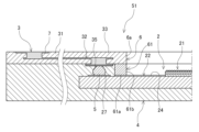
- a solid-state imaging device 51 according to the present embodiment differs from the first embodiment in that the metal bumps 5 are covered with an underfill portion 55 . As shown in FIG. 9 , the solid-state imaging device 51 has an underfill section 55 covering the metal bumps 5 .
- the underfill portion 55 is made of a material different from the encapsulating resin material forming the encapsulating resin portion 4 .
- the underfill portion 55 is made of a resin material, and is provided so as to cover at least a portion of the metal bumps 5 while filling the gaps between adjacent metal bumps 5 .
- the underfill portion 55 is a resin sealing portion that seals the gap between the image sensor 2 and the rewiring layer 3 .
- the underfill portion 55 is formed between the outer edge portion of the image sensor 2 and the peripheral area covering portion 33 of the rewiring layer 3 so as to enclose the plurality of metal bumps 5. . That is, the underfill portion 55 has an inner portion 55a located inside the metal bump 5 (right side in FIG. 9) and an outer portion 55b located outside the metal bump 5 (left side in FIG. 9). However, the underfill portion 55 may be provided on the metal bump 5 so as to cover only the outer surface portion of the metal bump 5 .
- the underfill portion 55 is a liquid hardening resin portion formed by hardening a pasty or liquid resin by baking or the like.
- the underfill portion 55 is, for example, a capillary flow type (capillary underfill) formed by causing a liquid resin with a relatively low viscosity to flow using capillary action.
- the material of the underfill portion 55 for example, a resin material used as a mold material is used.
- a thermosetting resin such as an epoxy resin or a thermosetting resin in which a filler containing silicon oxide as a main component is dispersed is used.
- a material having a lower viscosity than the material of the sealing resin portion 4 is used from the viewpoint of filling the gaps between the adjacent metal bumps 5 .
- the material of the underfill portion 55 is not particularly limited as long as it is different from the material of the sealing resin portion 4 .
- a liquid resin material for example, a thermosetting resin, hereinafter referred to as an "underfill material" that becomes the underfill portion 55 flows due to capillary action while being ejected from a dispenser nozzle, for example, and is provided in an array. It is applied so as to cover all or part of the plurality of metal bumps 5 and fill the gaps between the image sensor 2 and the rewiring layer 3 .
- the underfill portion 55 is a rectangular frame-shaped region corresponding to the shape of the portion where the image sensor 2 and the rewiring layer 3 overlap each other, that is, along the opening shape of the wiring layer opening portion 6. formed in
- the sealing resin material of the sealing resin portion 54 is forming an underfill portion 55 covering the metal bump 5 with a material different from that of the first step.
- the processes up to the step of forming the rewiring layer 43 on the support substrate 40 via the release layer 41 and the mask layer 44 and providing the image sensor 2 on the rewiring layer 43 are the same as those of the first embodiment. They are common (see FIGS. 5A, 5B, and 5C).
- a step of forming an underfill portion 55 is performed as shown in FIG. 10B.
- the underfill material is supplied to the gap between each image sensor 2 and the rewiring layer 43 (hereinafter referred to as "sensor-wiring gap") while being discharged from a nozzle of a dispenser (not shown).
- the underfill material is supplied from the outer peripheral side of the image sensor 2 to the sensor-wiring layer gap.
- the underfill material supplied to the sensor-wiring interlayer gap flows into the sensor-wiring interlayer gap in a manner of permeating into the sensor-wiring interlayer gap due to capillary action, covers the entire plurality of metal bumps 5, and covers the image sensor 2 and the rewiring layer. 43 so as to fill the gap between them.
- the underfill material for example, a material having a viscosity of about 10 Pa ⁇ s at room temperature is used.
- baking is performed under predetermined temperature conditions in order to evaporate the solvent contained in the underfill material and solidify the underfill material.
- the baking temperature is appropriately set according to the underfill material, the solvent contained therein, and the like.
- a hot plate, an oven, etc. are appropriately selected and used as necessary.
- a step of forming the sealing resin portion 54 is performed as shown in FIG. 10C. Thereafter, as in the first embodiment, the step of thinning the sealing resin portion 54 (see FIG. 6A), the step of peeling off the support substrate 40 (see FIG. 6B), and the step of individualizing by dicing (see FIG. 6B). 6C) is performed. Thereby, the solid-state imaging device 51 is obtained.
- the following effects are obtained. can get. That is, since the underfill portion 55 is provided between the peripheral region 22 of the image sensor 2 and the peripheral region covering portion 33 of the rewiring layer 3, when forming the sealing resin portion 54, the sealing resin material can be prevented from passing between the image sensor 2 and the rewiring layer 43 and entering the pixel region 21 of the image sensor 2 . Thereby, the function of the image sensor 2 can be ensured.
- the underfill portion 55 protects and reinforces the metal bumps 5 provided between the image sensor 2 and the rewiring layer 3 and the connection portions by the metal bumps 5. can be planned. Thereby, the bonding strength of the image sensor 2 to the rewiring layer 3 can be improved.
- the underfill portion 55 has an outer lower portion 55c that wraps around the image sensor 2 from the edge of the back surface 2b to cover the edges of the side surface 2c and the front surface 2a (step surface 24). Further, the underfill portion 55 does not have an inner portion 55a (see FIG. 9) with respect to the metal bump 5, but has an outer portion 55b positioned outside the metal bump 5. As shown in FIG.
- the formation mode of the underfill portion 55 may be a mode like this modified example.
- the shape of the underfill portion 55 can be appropriately changed by adjusting the discharge pressure of the underfill material from the nozzle, the application area of the underfill material, the viscosity of the underfill material, and the like. According to the configuration of this modified example as well, the underfill portion 55 can prevent the encapsulating resin material from entering the pixel region 21 side of the image sensor 2 in the process of forming the encapsulating resin portion 54 .
- a part of the interlayer insulating film 31 of the rewiring layer 3 forms a partition.
- the rewiring layer 3 serves as a part of the interlayer insulating film 31 and forms a partition at the opening edge of the wiring layer opening 6 between the arrangement space of the metal bumps 5 and the space on the pixel region 21 side. It has a partition wall portion 56 as a portion.
- the partition wall portion 56 is located inside the metal bump 5 (on the right side in FIG. 12), and is formed to protrude downward at the opening edge portion of the wiring layer opening portion 6 .
- the partition wall portion 56 forms the lower portion of the inner side surface 6a of the wiring layer opening 6 with its inner wall surface, and is linear or linear along the outer shape of the wiring layer opening 6 as a ridge portion having a predetermined thickness. It is formed in a rectangular frame shape.
- the partition wall portion 56 is formed so as to cover the entire or substantially the entire height range of the metal bumps 5 in the vertical direction.
- the partition wall portion 56 has a lower end surface 56a close to the stepped surface 24, which is a part of the surface 2a of the image sensor 2, with a slight gap therebetween. Due to the viscosity of the sealing resin material of the sealing resin portion 4, the sealing resin material enters the gap between the lower end surface 56a and the stepped surface 24 from the outside (left side in FIG. 12) to the pixel region 21 side.
- the gap is set to the extent that it does not occur.
- the partition wall portion 56 is formed of a lower layer portion of the interlayer insulating film 31 that constitutes the rewiring layer 3 , which will be the portion on the surface layer side of the rewiring layer 43 in the manufacturing process of the rewiring layer 3 .
- the partition wall portion 56 is formed in the lower layer portion of the interlayer insulating film 31 together with a concave portion 57 serving as an arrangement space for the metal bumps 5 .
- the concave portion 57 has an open side on the lower side, a bottom surface which is an upper surface, an inner wall surface, and an outer wall surface.
- the inner wall surface of the recess 57 serves as the outer wall surface 56 b of the partition wall portion 56 .
- a lower layer portion 58 that is the same layer portion as the partition wall portion 56 is formed outside the recess 57 .
- the recessed portion 57 is formed, for example, along the outer shape of the partition wall portion 56 so as to form a linear or rectangular frame-shaped groove portion.
- the concave portion 57 is a portion of the rewiring layer 3 that exposes the lower electrode 32 a that is connected to the upper side of the metal bump 5 through the plated layer 35 . Further, the recessed portion 57 is formed so as to include a formation region of the pad electrode 27 that receives connection on the lower side of the metal bump 5 in plan view.
- the opening side of the concave portion 57 is partially closed by the edge of the image sensor 2 , forming a space 59 around the metal bumps 5 together with the image sensor 2 .
- the concave portion 57 is formed so that the outer side of the space portion 59 is open in relation to the edge portion of the image sensor 2 , and is between the interlayer insulating film 31 of the rewiring layer 3 and the edge portion of the image sensor 2 .
- a gap 60 is formed in the .
- the recess 57 is filled with the sealing resin material of the sealing resin portion 4 , and the metal bumps 5 located in the recess 57 are embedded in the sealing resin portion 4 . That is, in this modified example, the sealing resin portion 4 has a recess filling portion 4 e that fills the recess 57 and entirely covers the connection portion of the metal bump 5 .
- the configuration of this modified example can be obtained, for example, by the following manufacturing method. That is, in the process of forming the rewiring layer 43, the layer portion of the insulating film 31x is formed on the surface side of the lower electrode 32a, and the concave portion 57 that exposes the lower electrode 32a is formed. partition walls 56 are formed. If the material of the insulating film is a photosensitive resin material, the recess 57 is formed by, for example, a photolithography process. Further, when the material of the insulating film is a non-photosensitive material, the concave portion 57 is formed using a laser or the like, for example.
- the sealing resin material is filled into the concave portion 57 through the gap 60 .
- the sealing resin material is blocked by the partition wall portion 56 .
- a partition section is provided to separate the arrangement space of the metal bumps 5 from the space on the pixel region 21 side.
- a partition is formed by a member different from the rewiring layer 3 and the image sensor 2 below the opening edge of the wiring layer opening 6 of the rewiring layer 3 .
- the solid-state imaging device 51 has a partition wall 61 as a partition portion that partitions the space on the side of the pixel region 21 from the arrangement space of the metal bumps 5 under the opening edge portion of the wiring layer opening portion 6 .
- the partition wall 61 is located inside the metal bump 5 (on the right side in FIG. 13), and is provided so as to protrude downward at the opening edge of the wiring layer opening 6 .
- the partition wall 61 forms a lower portion of the inner side surface 6a of the wiring layer opening 6 with an inner wall surface 61b, and has a linear or linear shape along the outer shape of the wiring layer opening 6 as a ridge portion having a predetermined thickness. It is provided in the shape of a rectangular frame.
- the partition wall 61 is provided so as to cover the entire or substantially the entire height range of the metal bumps 5 in the vertical direction.
- the partition wall 61 brings the lower end surface 61a close to the stepped surface 24, which is a part of the surface 2a of the image sensor 2, with a slight gap. Due to the viscosity of the sealing resin material of the sealing resin portion 4, the sealing resin material enters the gap between the lower end surface 61a and the stepped surface 24 from the outside (left side in FIG. 13) toward the pixel region 21 side.
- the gap is set to the extent that it does not occur.
- partition walls 61 are provided along the opening edges of the openings 46 of the rewiring layer 43 .
- the material of the partition wall 61 is, for example, a thermosetting resin such as an epoxy resin, a photosensitive adhesive such as a UV (ultraviolet) curable resin that is an acrylic resin, or a mixture thereof.
- a thermosetting resin such as an epoxy resin
- a photosensitive adhesive such as a UV (ultraviolet) curable resin that is an acrylic resin
- a non-photosensitive material is used as the material of the partition walls 61 .
- the partition wall 61 is formed, for example, by applying a material to the surface portion 43a (see FIG. 5B) of the rewiring layer 43 using a dispenser, patterning using photolithography, or the like.
- the partition wall 61 is provided by attaching a frame-shaped structure made of, for example, ceramics such as glass, an inorganic material such as metal or silicon, or a resin material to the rewiring layer 43 with an adhesive or the like. may be
- the sealing resin material is blocked by the partition wall 61, and the connection portion of the metal bump 5 is covered with the sealing resin material.
- the encapsulating resin material can be prevented from entering the pixel region 21 side of the image sensor 2. can be prevented.
- a dummy bump is provided inside the metal bump 5 using the same metal material as the metal bump 5.
- the dummy bumps are provided at positions corresponding to the gaps between adjacent metal bumps 5 so as to close the gaps.
- a solid-state imaging device 71 includes a second rewiring layer 73 on the sealing resin portion 4 side in addition to the rewiring layer 3 in comparison with the first embodiment. That is, the solid-state imaging device 71 is provided on the back surface 2b side of the image sensor 2 with respect to the image sensor 2 and the sealing resin portion 4, and is electrically connected to the rewiring layer 3 which is the first rewiring layer. A second rewiring layer 73 is further provided. In the solid-state imaging device 71, when the rewiring layer 3 is the front side rewiring layer, the second rewiring layer 73 is the back side rewiring layer.
- the back surface 2b of the image sensor 2 and the bottom surface 4b of the sealing resin part 4 form a flush bottom surface.
- the contact surface with respect to the image sensor 2 and the sealing resin portion 4 is the upper surface 73a.
- the second rewiring layer 73 is formed as a laminated wiring layer having a plurality of wiring layers 82 laminated with an interlayer insulating film 81 interposed therebetween.
- An upper layer electrode portion 82 a for receiving electrical connection to the rewiring layer 3 is formed by the uppermost layer portion of the wiring layer 82 constituting the second rewiring layer 73 .
- the upper layer electrode portion 82 a is an electrode portion that is exposed on the upper surface 73 a of the second rewiring layer 73 .
- the upper layer electrode portions 82a are formed at both end portions of the solid-state imaging device 71 . Note that the number and arrangement positions of the upper layer electrode portions 82a are not particularly limited.
- Each wiring layer 82 provided in the second rewiring layer 73 is formed to include a layered portion including an upper layer electrode portion 82a and a connection portion that connects the upper and lower layered portions.
- This connection portion is a portion formed in a connection via hole 81a formed in the interlayer insulating film 81 in the layer thickness direction.
- the second rewiring layer 73 may be a wiring layer having a single layer structure.
- the upper electrode portion 82a of the wiring layer 82 is electrically connected to the rewiring layer 3 by a metal bump 85 as a connection portion provided in the layer of the sealing resin portion 4.
- the rewiring layer 3 has a second lower layer electrode 32c as a portion to which the metal bump 85 is connected.
- the second lower layer electrode 32c is formed as an electrode portion in the same layer as the lower layer electrode 32a to which the metal bump 5 is connected.
- the second lower layer electrodes 32 c are provided at a plurality of locations corresponding to the arrangement of the metal bumps 85 .
- the metal bumps 85 are, for example, Au stud bumps, solder ball bumps, Au--Ag alloy bumps, or the like.
- the connecting portion between the rewiring layer 3 and the second rewiring layer 73 may be a metal post such as a Cu pillar, for example.
- the image sensor 2 and the sealing resin portion 54 are electrically connected to the rewiring layer 3 on the back surface 2 b side of the image sensor 2 .
- a step of forming a connected second rewiring layer 73 is provided.
- the steps up to the step of forming the rewiring layer 43 on the support substrate 40 via the release layer 41 and the mask layer 44 are the same as in the first embodiment (see FIGS. 5A and 5B).
- the metal bumps 85 are connected together with the lower-layer electrodes 32a to which the metal bumps 5 are connected.
- a second lower layer electrode 32c is formed.
- a plated layer (not shown) formed by Au displacement plating or the like is formed on the second lower layer electrode 32c by combining the materials of the second lower layer electrode 32c and the metal bump 85 or the like.
- a step of forming metal bumps 85 on the second lower layer electrodes 32c is performed.
- a wire bonding apparatus is used to form solder bumps as the metal bumps 85 on the second lower layer electrodes 32c.
- the metal post is formed on the second lower layer electrode 32c by plating, sputtering, vapor deposition, or the like using Cu, a Cu alloy, or the like as a material. A columnar protrusion is formed.
- the following steps are performed. First, after the resist for forming the wiring layer 32 of the rewiring layer 43 is removed, a seed layer is formed and the resist for forming Cu posts is patterned. After that, a Cu post having a desired height is formed on the seed layer by plating, the resist is peeled off, and the seed layer is removed by etching or the like.
- the image sensor 2 is mounted on the rewiring layer 43.
- a step of forming the sealing resin portion 54 is performed.
- the encapsulating resin portion 54 is formed such that the metal bumps 85 are embedded in the encapsulating resin material.
- a step of thinning the sealing resin portion 54 from the surface 54a side to a desired thickness by grinding is performed.
- the sealing resin portion 54 is ground until at least the metal bumps 85 are exposed on the surface 54 a of the sealing resin portion 54 .
- the rear surface 2b of the image sensor 2 is also exposed.
- the chip back layer portion 54f may be formed in the sealing resin portion 54 without exposing the back surface 2b of the image sensor 2.
- the metal bumps 85 are ground together with the sealing resin portion 54 so that a sufficient area for ensuring electrical connection to the second rewiring layer 73 is exposed. receive. Therefore, in the metal bump 85, an end surface 85a that forms a flat surface 86 that is flush with the surface 54a of the sealing resin portion 54 is formed on the opposite side (upper side in FIG. 16B) of the connection side to the second lower layer electrode 32c. .
- the flat surface 86 is the surface on which the second rewiring layer 73 is formed. In the example shown in FIG. 16B , flat surface 86 is formed by front surface 54 a of sealing resin portion 54 , end surface 85 a of metal bump 85 and back surface 2 b of image sensor 2 .
- a second rewiring layer 93 is formed on the flat surface 86, as shown in FIG. 16C.
- the second rewiring layer 93 is a portion forming the second rewiring layer 73 in the solid-state imaging device 71 obtained by singulation.
- a known method such as a semi-additive method is used in the same manner as in the step of forming the rewiring layer 43 according to the first embodiment.
- a second rewiring layer 93 having a laminated structure that becomes the wiring layer 82 is formed.
- the step of peeling off the support substrate 40 (see FIG. 6B) and the step of singulating by dicing (see FIG. 6C) are performed.
- a solid-state imaging device 71 having a rewiring layer 3 as a front side rewiring layer and a second rewiring layer 73 as a back side rewiring layer is obtained.
- the solid-state imaging device 71 and the method for manufacturing the same according to the present embodiment in addition to the effects obtained by the solid-state imaging device 1 and the method for manufacturing the same according to the first embodiment, the following effects are obtained. can get. That is, according to the configuration according to the present embodiment, in addition to the rewiring layer 3, the second rewiring layer 73 provided to the rewiring layer 3 via the sealing resin portion 54 is provided. Multi-layering of rewiring layers can be accommodated. For example, by providing an external connection terminal on the surface layer side (lower side in FIG. 14) of the second rewiring layer 73, an electronic component such as a flexible substrate can be connected to the second rewiring layer 73. It becomes possible.
- the second rewiring layer 73 can compensate for the number of wiring layers, in the step of forming the rewiring layer 43, the separation layer 41 or the like is interposed between the support substrate 40 such as a glass plate and the like. It is possible to reduce the number of wiring layers to be formed. This makes it possible to reduce the warping of the rewiring layer 43 during the manufacturing process, and furthermore to reduce the warping of the entire package in the solid-state imaging device 71 after completion.
- Configuration example of electronic device> An application example of the solid-state imaging device according to the embodiment described above to an electronic device will be described with reference to FIG. 17 .
- the solid-state imaging device includes camera devices such as digital still cameras and video cameras, mobile terminal devices having an imaging function, and copiers that use a solid-state imaging device as an image reading unit. It is applicable to general electronic equipment that uses a solid-state image pickup device in the part).
- the solid-state imaging device may be formed as a single chip, or may be in the form of a module having an imaging function in which an imaging section and a signal processing section or an optical system are packaged together.
- a camera device 200 as an electronic device includes an optical unit 202, a solid-state imaging device 201, a DSP (Digital Signal Processor) circuit 203 as a camera signal processing circuit, a frame memory 204, and a display unit. 205 , a recording unit 206 , an operation unit 207 , and a power supply unit 208 .
- the DSP circuit 203, frame memory 204, display unit 205, recording unit 206, operation unit 207, and power supply unit 208 are appropriately connected via a connection line 209 such as a bus line.
- the solid-state imaging device 201 is, for example, the solid-state imaging device 1 according to the first embodiment described above.
- the optical unit 202 includes a plurality of lenses, takes in incident light (image light) from a subject, and forms an image on the imaging surface of the solid-state imaging device 201 .
- the solid-state imaging device 201 converts the amount of incident light imaged on the imaging surface by the optical unit 202 into an electric signal on a pixel-by-pixel basis, and outputs the electric signal as a pixel signal.
- the display unit 205 is, for example, a panel type display device such as a liquid crystal panel or an organic EL (Electro Luminescence) panel, and displays moving images or still images captured by the solid-state imaging device 201 .
- a recording unit 206 records a moving image or still image captured by the solid-state imaging device 201 in a recording medium such as a hard disk or a semiconductor memory.
- the operation unit 207 issues operation commands for various functions of the camera device 200 under the user's operation.
- the power supply unit 208 appropriately supplies various power supplies as operating power supplies for the DSP circuit 203, the frame memory 204, the display unit 205, the recording unit 206, and the operation unit 207 to these supply targets.
- the camera device 200 As described above, regarding the solid-state imaging device 201, it is possible to reduce the size, height, and speed of the device without impairing the imaging performance of the image sensor 2. As a result, the camera device 200 can be maintained in a good operating state, desired characteristics can be obtained, and the device can be made compact.
- the image sensor 2 has steps between the pixel region 21 and the peripheral region 22 on the surface 2a side, which is the pixel forming surface side. It is not limited to the one with a simple configuration.
- the imaging device according to the present technology may have a configuration in which the surface is flat without having steps on the pixel forming surface side.
- this technique can take the following configurations. (1) an imaging device having a pixel region in which a large number of pixels are formed and a peripheral region that is a region surrounding the pixel region on the surface side; a rewiring layer having an opening formed in a shape; a sealing resin portion formed of a sealing resin material and provided so as to cover the periphery of the imaging element and the back side of the rewiring layer; and a connection section provided on the peripheral region of the image pickup device and electrically connecting the image pickup device and the rewiring layer.
- the rewiring layer has a peripheral area covering portion that covers at least a portion of the peripheral area of the imaging device in plan view,
- the imaging element has a stepped surface forming a step on a lower side with respect to the pixel region in the peripheral region;
- the imaging device according to any one of (1) to (4), wherein the connection section is provided on the step surface.
- the wall surface forming the opening is an inclined surface that is inclined so as to gradually widen the opening area of the opening from the front surface side to the back surface side of the rewiring layer. ).
- a partition portion is provided between the rewiring layer and the imaging element on the pixel region side of the connection portion to separate the arrangement space of the connection portion from the space on the pixel region side.
- an imaging element having a pixel region in which a large number of pixels are formed and a peripheral region that is a region around the pixel region on the surface side; a rewiring layer provided on the surface side of the imaging element and having an opening penetrating a region including the pixel region; a sealing resin portion formed of a sealing resin material and provided so as to cover the periphery of the imaging element and the back side of the rewiring layer;
- An electronic device comprising an imaging device, comprising: a connection section provided on the peripheral region of the imaging element and electrically connecting the imaging element and the rewiring layer.
- a second rewiring layer electrically connected to the rewiring layer is formed on the back surface side of the imaging device with respect to the imaging device and the sealing resin portion.
Landscapes
- Solid State Image Pick-Up Elements (AREA)
- Transforming Light Signals Into Electric Signals (AREA)
Abstract
Description
1.第1実施形態に係る固体撮像装置の構成例
2.第1実施形態に係る固体撮像装置の製造方法
3.第1実施形態に係る固体撮像装置の変形例
4.第2実施形態に係る固体撮像装置の構成例
5.第2実施形態に係る固体撮像装置の製造方法
6.第2実施形態に係る固体撮像装置の変形例
7.第3実施形態に係る固体撮像装置の構成例
8.第3実施形態に係る固体撮像装置の製造方法
9.電子機器の構成例
本技術の第1実施形態に係る固体撮像装置1の構成例について、図1から図4を参照して説明する。なお、図1における上下方向を固体撮像装置1における上下方向とする。
第1実施形態に係る固体撮像装置1の製造方法の一例について、図5および図6を参照して説明する。
(1)デバイス構造形成時には、支持基板40とデバイス構造物が剥離することがない。
(2)デバイス構造物を支持基板40から剥離する際には、デバイス構造物側にダメージを与えない
(A)機械的剥離:ブレード等で剥離
(B)化学的反応:光、熱など
(C)物理的反応:レーザアブレーションなど
上記(B)、(C)による剥離層41の場合、外部からエネルギーを与えられることにより剥離層41を構成する材料の状態が変化し、支持基板40とデバイス構造物が分離可能な状態となる。剥離材としては、例えば、UV(紫外線)光やレーザ光等の光を照射することや加熱すること等により易剥離の状態(粘着力が低下した状態)となる材料が用いられる。UV易剥離タイプの剥離材は、例えばUVを照射することにより粘着力が低下する粘着剤となる。また、剥離材としては、例えば、UV硬化性樹脂等の光硬化性の材料を用いることができる。
第1実施形態に係る固体撮像装置1の変形例について説明する。
第1の変形例は、再配線層3の構成についての変形例である。図7に示すように、第1の変形例では、再配線層3は、配線層開口部6をなす壁面である内側面6aを、再配線層3の表面側(表面部1a側)から裏面側(裏面部1b側)にかけて配線層開口部6の開口面積を徐々に広げるように傾斜した傾斜面としている。配線層開口部6の四方の内側面6aは、再配線層3の層厚方向について、イメージセンサ2側(図7における下側)からその反対側(図7における上側)にかけて外側から内側に向かう方向、つまり配線層開口部6の開口幅を狭める方向に傾斜している。
第2の変形例は、固体撮像装置1の製造方法において用いる支持基板40の剥離方法についての変形例である。第2の変形例では、支持基板40を機械的に剥離させる方法が用いられる。
本技術の第2実施形態に係る固体撮像装置51の構成例について、図9を参照して説明する。以下に説明する各実施形態では、第1実施形態と共通の構成については同一の符号を付し、重複する内容についての説明を適宜省略する。
第2実施形態に係る固体撮像装置51の製造方法の一例について、図10を参照して説明する。
第2実施形態に係る固体撮像装置51の変形例について説明する。以下に説明する変形例は、封止樹脂部54を形成する際に封止樹脂材料がイメージセンサ2と再配線層43との間を通過して画素領域21へと浸入することを防止するための構成に関する変形例である。
第2の変形例では、金属バンプ5に対して画素領域21側に、再配線層3の周辺領域被覆部33とイメージセンサ2の周辺領域22との間で、金属バンプ5の配置空間と画素領域21側の空間とを仕切る仕切部が設けられている。
第3の変形例では、第2の変形例と同様に、金属バンプ5の配置空間と画素領域21側の空間とを仕切る仕切部が設けられている。図13に示すように、本変形例では、再配線層3の配線層開口部6の開口縁部の下側において、再配線層3およびイメージセンサ2とは別の部材により仕切部が形成されている。つまり、本変形例において、固体撮像装置51は、配線層開口部6の開口縁部の下側に、金属バンプ5の配置空間と画素領域21側の空間とを仕切る仕切部としての仕切壁61を有する。
本技術の第3実施形態に係る固体撮像装置71の構成例について、図14を参照して説明する。
第3実施形態に係る固体撮像装置71の製造方法の一例について、図15および図16を参照して説明する。
上述した実施形態に係る固体撮像装置の電子機器への適用例について、図17を用いて説明する。
(1)
表面側に、多数の画素が形成された画素領域、および前記画素領域の周囲の領域である周辺領域を有する撮像素子と、 前記撮像素子の表面側に設けられ、前記画素領域を含む領域に貫通状に形成された開口部を有する再配線層と、
封止樹脂材料により形成され、前記撮像素子の周囲および前記再配線層の裏面側を被覆するように設けられた封止樹脂部と、
前記撮像素子の前記周辺領域上に設けられ、前記撮像素子と前記再配線層とを電気的に接続する接続部と、を備えた
撮像装置。
(2)
前記再配線層は、平面視で前記撮像素子の前記周辺領域の少なくとも一部を覆う周辺領域被覆部を有し、
前記接続部は、前記撮像素子と前記周辺領域被覆部との間に設けられている
前記(1)に記載の撮像装置。
(3)
前記撮像素子は、前記封止樹脂部に形成された凹部内に位置し、前記封止樹脂部の層厚の範囲内に設けられている
前記(1)または前記(2)に記載の撮像装置。
(4)
前記封止樹脂材料とは異なる材料により形成され、前記接続部を覆うアンダーフィル部をさらに備えた
前記(1)~(3)のいずれか1つに記載の撮像装置。
(5)
前記撮像素子は、前記周辺領域に、前記画素領域に対して低い側に段差をなす段差面を有し、
前記接続部は、前記段差面上に設けられている
前記(1)~(4)のいずれか1つに記載の撮像装置。
(6)
前記再配線層は、前記開口部をなす壁面を、前記再配線層の表面側から裏面側にかけて前記開口部の開口面積を徐々に広げるように傾斜した傾斜面としている
前記(1)~(5)のいずれか1つに記載の撮像装置。
(7)
前記接続部に対して前記画素領域側に、前記再配線層と前記撮像素子との間で、前記接続部の配置空間と前記画素領域側の空間とを仕切る仕切部が設けられている
前記(1)~(5)のいずれか1つに記載の撮像装置。
(8)
前記撮像素子および前記封止樹脂部に対して前記撮像素子の裏面側に設けられ、前記再配線層と電気的に接続された第2の再配線層をさらに備えた
前記(1)~(7)のいずれか1つに記載の撮像装置。
(9)
表面側に、多数の画素が形成された画素領域、および前記画素領域の周囲の領域である周辺領域を有する撮像素子と、
前記撮像素子の表面側に設けられ、前記画素領域を含む領域に貫通状に形成された開口部を有する再配線層と、
封止樹脂材料により形成され、前記撮像素子の周囲および前記再配線層の裏面側を被覆するように設けられた封止樹脂部と、
前記撮像素子の前記周辺領域上に設けられ、前記撮像素子と前記再配線層とを電気的に接続する接続部と、を備えた
撮像装置を有する
電子機器。
(10)
支持基板の一方の板面に剥離層を有する支持部材を準備する工程と、 前記剥離層の上に、前記剥離層を露出させる開口部を有する再配線層を形成する工程と、
前記再配線層の上に、撮像素子を、前記撮像素子の表面側を前記剥離層側とする向きで前記開口部を覆うとともに、前記再配線層と電気的に接続させた状態で設ける工程と、
封止樹脂材料により、前記再配線層の前記剥離層側と反対側および前記撮像素子の周囲を被覆するように封止樹脂部を形成する工程と、
前記剥離層により前記支持基板を前記再配線層から剥離する工程と、を含む
撮像装置の製造方法。
(11)
前記封止樹脂部を形成する工程の後に、前記封止樹脂部を、前記再配線層側と反対側から薄くする工程を有する
前記(10)に記載の撮像装置の製造方法。
(12)
前記撮像素子を設ける工程の後、かつ前記封止樹脂部を形成する工程の前に、前記封止樹脂材料とは異なる材料により、前記接続部を覆うアンダーフィル部を形成する工程を有する
前記(10)または前記(11)に記載の撮像装置の製造方法。
(13)
前記再配線層を形成する工程では、前記開口部をなす壁面が、前記剥離層側から前記剥離層側と反対側にかけて前記開口部の開口面積を徐々に広げるように傾斜した傾斜面となるように、前記再配線層を形成する
前記(10)~(12)のいずれか1つに記載の撮像装置の製造方法。
(14)
前記封止樹脂部を形成する工程の後に、前記撮像素子および前記封止樹脂部に対して前記撮像素子の裏面側に、前記再配線層と電気的に接続された第2の再配線層を形成する工程を有する
前記(10)~(13)のいずれか1つに記載の撮像装置の製造方法。
1a 表面部
1b 裏面部
2 イメージセンサ(撮像素子)
2a 表面
3 再配線層
3b 裏面
4 封止樹脂部
4d 凹部
5 金属バンプ(接続部)
6 配線層開口部
6a 内側面(壁面)
7 外部接続端子
20 半導体基板
21 画素領域
22 周辺領域
23 画素
24 段差面
31 層間絶縁膜
32 配線層
32a 下層電極
32c 第2下層電極
33 周辺領域被覆部
40 支持基板
40a 上面
41 剥離層
42 支持部材
43 再配線層
46 開口部
46a 内側面(壁面)
51 固体撮像装置(撮像装置)
54 封止樹脂部
54a 表面
55 アンダーフィル部
56 仕切壁部(仕切部)
61 仕切壁(仕切部)
71 固体撮像装置(撮像装置)
73 第2の再配線層
85 金属バンプ
93 第2の再配線層
200 カメラ装置(電子機器)
201 固体撮像装置(撮像装置)
Claims (14)
- 表面側に、多数の画素が形成された画素領域、および前記画素領域の周囲の領域である周辺領域を有する撮像素子と、
前記撮像素子の表面側に設けられ、前記画素領域を含む領域に貫通状に形成された開口部を有する再配線層と、
封止樹脂材料により形成され、前記撮像素子の周囲および前記再配線層の裏面側を被覆するように設けられた封止樹脂部と、
前記撮像素子の前記周辺領域上に設けられ、前記撮像素子と前記再配線層とを電気的に接続する接続部と、を備えた
撮像装置。 - 前記再配線層は、平面視で前記撮像素子の前記周辺領域の少なくとも一部を覆う周辺領域被覆部を有し、
前記接続部は、前記撮像素子と前記周辺領域被覆部との間に設けられている
請求項1に記載の撮像装置。 - 前記撮像素子は、前記封止樹脂部に形成された凹部内に位置し、前記封止樹脂部の層厚の範囲内に設けられている
請求項1に記載の撮像装置。 - 前記封止樹脂材料とは異なる材料により形成され、前記接続部を覆うアンダーフィル部をさらに備えた
請求項1に記載の撮像装置。 - 前記撮像素子は、前記周辺領域に、前記画素領域に対して低い側に段差をなす段差面を有し、
前記接続部は、前記段差面上に設けられている
請求項1に記載の撮像装置。 - 前記再配線層は、前記開口部をなす壁面を、前記再配線層の表面側から裏面側にかけて前記開口部の開口面積を徐々に広げるように傾斜した傾斜面としている
請求項1に記載の撮像装置。 - 前記接続部に対して前記画素領域側に、前記再配線層と前記撮像素子との間で、前記接続部の配置空間と前記画素領域側の空間とを仕切る仕切部が設けられている
請求項1に記載の撮像装置。 - 前記撮像素子および前記封止樹脂部に対して前記撮像素子の裏面側に設けられ、前記再配線層と電気的に接続された第2の再配線層をさらに備えた
請求項1に記載の撮像装置。 - 表面側に、多数の画素が形成された画素領域、および前記画素領域の周囲の領域である周辺領域を有する撮像素子と、
前記撮像素子の表面側に設けられ、前記画素領域を含む領域に貫通状に形成された開口部を有する再配線層と、
封止樹脂材料により形成され、前記撮像素子の周囲および前記再配線層の裏面側を被覆するように設けられた封止樹脂部と、
前記撮像素子の前記周辺領域上に設けられ、前記撮像素子と前記再配線層とを電気的に接続する接続部と、を備えた 撮像装置を有する
電子機器。 - 支持基板の一方の板面に剥離層を有する支持部材を準備する工程と、
前記剥離層の上に、前記剥離層を露出させる開口部を有する再配線層を形成する工程と、
前記再配線層の上に、撮像素子を、前記撮像素子の表面側を前記剥離層側とする向きで前記開口部を覆うとともに、前記再配線層と電気的に接続させた状態で設ける工程と、
封止樹脂材料により、前記再配線層の前記剥離層側と反対側および前記撮像素子の周囲を被覆するように封止樹脂部を形成する工程と、
前記剥離層により前記支持基板を前記再配線層から剥離する工程と、を含む
撮像装置の製造方法。 - 前記封止樹脂部を形成する工程の後に、前記封止樹脂部を、前記再配線層側と反対側から薄くする工程を有する
請求項10に記載の撮像装置の製造方法。 - 前記撮像素子を設ける工程の後、かつ前記封止樹脂部を形成する工程の前に、前記封止樹脂材料とは異なる材料により、前記接続部を覆うアンダーフィル部を形成する工程を有する
請求項10に記載の撮像装置の製造方法。 - 前記再配線層を形成する工程では、前記開口部をなす壁面が、前記剥離層側から前記剥離層側と反対側にかけて前記開口部の開口面積を徐々に広げるように傾斜した傾斜面となるように、前記再配線層を形成する
請求項10に記載の撮像装置の製造方法。 - 前記封止樹脂部を形成する工程の後に、前記撮像素子および前記封止樹脂部に対して前記撮像素子の裏面側に、前記再配線層と電気的に接続された第2の再配線層を形成する工程を有する
請求項10に記載の撮像装置の製造方法。
Priority Applications (5)
| Application Number | Priority Date | Filing Date | Title |
|---|---|---|---|
| KR1020247010563A KR20240073033A (ko) | 2021-09-30 | 2022-03-14 | 촬상 장치, 전자 기기 및 촬상 장치의 제조 방법 |
| US18/692,495 US20250255028A1 (en) | 2021-09-30 | 2022-03-14 | Imaging device, electronic device, and method for manufacturing imaging device |
| JP2023551032A JPWO2023053503A1 (ja) | 2021-09-30 | 2022-03-14 | |
| EP22875386.9A EP4411803A4 (en) | 2021-09-30 | 2022-03-14 | Imaging device, electronic apparatus, and method for manufacturing imaging device |
| CN202280064164.3A CN117981085A (zh) | 2021-09-30 | 2022-03-14 | 成像设备、电子设备以及成像设备的制造方法 |
Applications Claiming Priority (2)
| Application Number | Priority Date | Filing Date | Title |
|---|---|---|---|
| JP2021161007 | 2021-09-30 | ||
| JP2021-161007 | 2021-09-30 |
Publications (1)
| Publication Number | Publication Date |
|---|---|
| WO2023053503A1 true WO2023053503A1 (ja) | 2023-04-06 |
Family
ID=85782162
Family Applications (1)
| Application Number | Title | Priority Date | Filing Date |
|---|---|---|---|
| PCT/JP2022/011295 Ceased WO2023053503A1 (ja) | 2021-09-30 | 2022-03-14 | 撮像装置、電子機器および撮像装置の製造方法 |
Country Status (6)
| Country | Link |
|---|---|
| US (1) | US20250255028A1 (ja) |
| EP (1) | EP4411803A4 (ja) |
| JP (1) | JPWO2023053503A1 (ja) |
| KR (1) | KR20240073033A (ja) |
| CN (1) | CN117981085A (ja) |
| WO (1) | WO2023053503A1 (ja) |
Citations (6)
| Publication number | Priority date | Publication date | Assignee | Title |
|---|---|---|---|---|
| JP2004327917A (ja) * | 2003-04-28 | 2004-11-18 | Matsushita Electric Ind Co Ltd | 固体撮像装置の製造方法 |
| JP2005317564A (ja) * | 2004-04-26 | 2005-11-10 | Matsushita Electric Ind Co Ltd | 光学デバイスおよびその製造方法 |
| JP2008263551A (ja) * | 2007-04-13 | 2008-10-30 | Matsushita Electric Ind Co Ltd | 固体撮像装置およびその製造方法 |
| US9349764B1 (en) * | 2014-12-29 | 2016-05-24 | SK Hynix Inc. | Embedded image sensor packages and methods of fabricating the same |
| CN207503979U (zh) * | 2017-09-06 | 2018-06-15 | 中芯长电半导体(江阴)有限公司 | Cmos图像传感器扇出型封装结构 |
| JP2019216187A (ja) * | 2018-06-13 | 2019-12-19 | ソニーセミコンダクタソリューションズ株式会社 | 撮像装置 |
Family Cites Families (5)
| Publication number | Priority date | Publication date | Assignee | Title |
|---|---|---|---|---|
| US7459729B2 (en) * | 2006-12-29 | 2008-12-02 | Advanced Chip Engineering Technology, Inc. | Semiconductor image device package with die receiving through-hole and method of the same |
| US10763286B2 (en) * | 2015-07-23 | 2020-09-01 | Sony Corporation | Semiconductor device, manufacturing method thereof, and electronic apparatus |
| KR102015910B1 (ko) * | 2018-01-24 | 2019-10-23 | 삼성전자주식회사 | 팬-아웃 센서 패키지 |
| CN208638447U (zh) * | 2018-06-29 | 2019-03-22 | 宁波舜宇光电信息有限公司 | 线路板组件、感光组件及摄像模组 |
| CN110752225B (zh) * | 2018-07-23 | 2022-07-12 | 宁波舜宇光电信息有限公司 | 感光组件及其制作方法 |
-
2022
- 2022-03-14 KR KR1020247010563A patent/KR20240073033A/ko active Pending
- 2022-03-14 WO PCT/JP2022/011295 patent/WO2023053503A1/ja not_active Ceased
- 2022-03-14 CN CN202280064164.3A patent/CN117981085A/zh not_active Withdrawn
- 2022-03-14 US US18/692,495 patent/US20250255028A1/en active Pending
- 2022-03-14 EP EP22875386.9A patent/EP4411803A4/en not_active Withdrawn
- 2022-03-14 JP JP2023551032A patent/JPWO2023053503A1/ja active Pending
Patent Citations (6)
| Publication number | Priority date | Publication date | Assignee | Title |
|---|---|---|---|---|
| JP2004327917A (ja) * | 2003-04-28 | 2004-11-18 | Matsushita Electric Ind Co Ltd | 固体撮像装置の製造方法 |
| JP2005317564A (ja) * | 2004-04-26 | 2005-11-10 | Matsushita Electric Ind Co Ltd | 光学デバイスおよびその製造方法 |
| JP2008263551A (ja) * | 2007-04-13 | 2008-10-30 | Matsushita Electric Ind Co Ltd | 固体撮像装置およびその製造方法 |
| US9349764B1 (en) * | 2014-12-29 | 2016-05-24 | SK Hynix Inc. | Embedded image sensor packages and methods of fabricating the same |
| CN207503979U (zh) * | 2017-09-06 | 2018-06-15 | 中芯长电半导体(江阴)有限公司 | Cmos图像传感器扇出型封装结构 |
| JP2019216187A (ja) * | 2018-06-13 | 2019-12-19 | ソニーセミコンダクタソリューションズ株式会社 | 撮像装置 |
Non-Patent Citations (1)
| Title |
|---|
| See also references of EP4411803A4 * |
Also Published As
| Publication number | Publication date |
|---|---|
| EP4411803A4 (en) | 2025-06-25 |
| US20250255028A1 (en) | 2025-08-07 |
| JPWO2023053503A1 (ja) | 2023-04-06 |
| KR20240073033A (ko) | 2024-05-24 |
| EP4411803A1 (en) | 2024-08-07 |
| CN117981085A (zh) | 2024-05-03 |
Similar Documents
| Publication | Publication Date | Title |
|---|---|---|
| TWI253149B (en) | Semiconductor device, module for optical devices, and manufacturing method of semiconductor device | |
| CN101937894B (zh) | 具有贯通电极的半导体器件及其制造方法 | |
| US7919348B2 (en) | Methods for protecting imaging elements of photoimagers during back side processing | |
| US7893514B2 (en) | Image sensor package, method of manufacturing the same, and image sensor module including the image sensor package | |
| TWI686937B (zh) | 形成影像感測器積體電路封裝之方法 | |
| US7439094B2 (en) | Method of manufacturing a semiconductor package | |
| US9230947B2 (en) | Method of forming 3D integrated microelectronic assembly with stress reducing interconnects | |
| US7593636B2 (en) | Pin referenced image sensor to reduce tilt in a camera module | |
| KR100866619B1 (ko) | 웨이퍼 레벨의 이미지센서 모듈 및 그 제조방법, 그리고카메라 모듈 | |
| JP5078725B2 (ja) | 半導体装置 | |
| US11282879B2 (en) | Image sensor packaging method, image sensor packaging structure, and lens module | |
| US20140312506A1 (en) | Semiconductor device and method for manufacturing same | |
| US9966400B2 (en) | Photosensitive module and method for forming the same | |
| CN103943645A (zh) | 影像传感器模组及其形成方法 | |
| WO2020103215A1 (zh) | 摄像组件及其封装方法、镜头模组、电子设备 | |
| KR20210080718A (ko) | 반도체 패키지 | |
| TWI501359B (zh) | 電子元件封裝體及其形成方法 | |
| JP7389029B2 (ja) | 固体撮像装置、電子機器、および固体撮像装置の製造方法 | |
| US9978788B2 (en) | Photosensitive module and method for forming the same | |
| WO2023053503A1 (ja) | 撮像装置、電子機器および撮像装置の製造方法 | |
| CN112151560A (zh) | 图像传感器封装件和相关方法 | |
| US20230290710A1 (en) | Manufacturing method of semiconductor device, semiconductor device, and electronic apparatus | |
| KR20220051470A (ko) | 반도체 패키지 및 이의 제조 방법 |
Legal Events
| Date | Code | Title | Description |
|---|---|---|---|
| 121 | Ep: the epo has been informed by wipo that ep was designated in this application |
Ref document number: 22875386 Country of ref document: EP Kind code of ref document: A1 |
|
| WWE | Wipo information: entry into national phase |
Ref document number: 2023551032 Country of ref document: JP |
|
| WWE | Wipo information: entry into national phase |
Ref document number: 202280064164.3 Country of ref document: CN |
|
| ENP | Entry into the national phase |
Ref document number: 20247010563 Country of ref document: KR Kind code of ref document: A |
|
| NENP | Non-entry into the national phase |
Ref country code: DE |
|
| ENP | Entry into the national phase |
Ref document number: 2022875386 Country of ref document: EP Effective date: 20240430 |
|
| WWP | Wipo information: published in national office |
Ref document number: 18692495 Country of ref document: US |
|
| WWW | Wipo information: withdrawn in national office |
Ref document number: 2022875386 Country of ref document: EP |