WO2023058720A1 - 撮像装置 - Google Patents
撮像装置 Download PDFInfo
- Publication number
- WO2023058720A1 WO2023058720A1 PCT/JP2022/037463 JP2022037463W WO2023058720A1 WO 2023058720 A1 WO2023058720 A1 WO 2023058720A1 JP 2022037463 W JP2022037463 W JP 2022037463W WO 2023058720 A1 WO2023058720 A1 WO 2023058720A1
- Authority
- WO
- WIPO (PCT)
- Prior art keywords
- circuit
- pixel
- photoelectric conversion
- signal
- imaging device
- Prior art date
- Legal status (The legal status is an assumption and is not a legal conclusion. Google has not performed a legal analysis and makes no representation as to the accuracy of the status listed.)
- Ceased
Links
Images













Classifications
-
- H—ELECTRICITY
- H04—ELECTRIC COMMUNICATION TECHNIQUE
- H04N—PICTORIAL COMMUNICATION, e.g. TELEVISION
- H04N25/00—Circuitry of solid-state image sensors [SSIS]; Control thereof
- H04N25/70—SSIS architectures; Circuits associated therewith
- H04N25/76—Addressed sensors, e.g. MOS or CMOS sensors
- H04N25/78—Readout circuits for addressed sensors, e.g. output amplifiers or A/D converters
-
- H—ELECTRICITY
- H10—SEMICONDUCTOR DEVICES; ELECTRIC SOLID-STATE DEVICES NOT OTHERWISE PROVIDED FOR
- H10F—INORGANIC SEMICONDUCTOR DEVICES SENSITIVE TO INFRARED RADIATION, LIGHT, ELECTROMAGNETIC RADIATION OF SHORTER WAVELENGTH OR CORPUSCULAR RADIATION
- H10F39/00—Integrated devices, or assemblies of multiple devices, comprising at least one element covered by group H10F30/00, e.g. radiation detectors comprising photodiode arrays
- H10F39/10—Integrated devices
- H10F39/12—Image sensors
-
- H—ELECTRICITY
- H04—ELECTRIC COMMUNICATION TECHNIQUE
- H04N—PICTORIAL COMMUNICATION, e.g. TELEVISION
- H04N25/00—Circuitry of solid-state image sensors [SSIS]; Control thereof
- H04N25/40—Extracting pixel data from image sensors by controlling scanning circuits, e.g. by modifying the number of pixels sampled or to be sampled
- H04N25/44—Extracting pixel data from image sensors by controlling scanning circuits, e.g. by modifying the number of pixels sampled or to be sampled by partially reading an SSIS array
- H04N25/441—Extracting pixel data from image sensors by controlling scanning circuits, e.g. by modifying the number of pixels sampled or to be sampled by partially reading an SSIS array by reading contiguous pixels from selected rows or columns of the array, e.g. interlaced scanning
-
- H—ELECTRICITY
- H04—ELECTRIC COMMUNICATION TECHNIQUE
- H04N—PICTORIAL COMMUNICATION, e.g. TELEVISION
- H04N25/00—Circuitry of solid-state image sensors [SSIS]; Control thereof
- H04N25/70—SSIS architectures; Circuits associated therewith
- H04N25/76—Addressed sensors, e.g. MOS or CMOS sensors
- H04N25/77—Pixel circuitry, e.g. memories, A/D converters, pixel amplifiers, shared circuits or shared components
-
- H—ELECTRICITY
- H04—ELECTRIC COMMUNICATION TECHNIQUE
- H04N—PICTORIAL COMMUNICATION, e.g. TELEVISION
- H04N25/00—Circuitry of solid-state image sensors [SSIS]; Control thereof
- H04N25/70—SSIS architectures; Circuits associated therewith
- H04N25/76—Addressed sensors, e.g. MOS or CMOS sensors
- H04N25/77—Pixel circuitry, e.g. memories, A/D converters, pixel amplifiers, shared circuits or shared components
- H04N25/772—Pixel circuitry, e.g. memories, A/D converters, pixel amplifiers, shared circuits or shared components comprising A/D, V/T, V/F, I/T or I/F converters
-
- H—ELECTRICITY
- H04—ELECTRIC COMMUNICATION TECHNIQUE
- H04N—PICTORIAL COMMUNICATION, e.g. TELEVISION
- H04N25/00—Circuitry of solid-state image sensors [SSIS]; Control thereof
- H04N25/70—SSIS architectures; Circuits associated therewith
- H04N25/79—Arrangements of circuitry being divided between different or multiple substrates, chips or circuit boards, e.g. stacked image sensors
-
- H—ELECTRICITY
- H10—SEMICONDUCTOR DEVICES; ELECTRIC SOLID-STATE DEVICES NOT OTHERWISE PROVIDED FOR
- H10F—INORGANIC SEMICONDUCTOR DEVICES SENSITIVE TO INFRARED RADIATION, LIGHT, ELECTROMAGNETIC RADIATION OF SHORTER WAVELENGTH OR CORPUSCULAR RADIATION
- H10F39/00—Integrated devices, or assemblies of multiple devices, comprising at least one element covered by group H10F30/00, e.g. radiation detectors comprising photodiode arrays
- H10F39/10—Integrated devices
- H10F39/12—Image sensors
- H10F39/199—Back-illuminated image sensors
-
- H—ELECTRICITY
- H10—SEMICONDUCTOR DEVICES; ELECTRIC SOLID-STATE DEVICES NOT OTHERWISE PROVIDED FOR
- H10F—INORGANIC SEMICONDUCTOR DEVICES SENSITIVE TO INFRARED RADIATION, LIGHT, ELECTROMAGNETIC RADIATION OF SHORTER WAVELENGTH OR CORPUSCULAR RADIATION
- H10F39/00—Integrated devices, or assemblies of multiple devices, comprising at least one element covered by group H10F30/00, e.g. radiation detectors comprising photodiode arrays
- H10F39/80—Constructional details of image sensors
- H10F39/809—Constructional details of image sensors of hybrid image sensors
-
- H—ELECTRICITY
- H10—SEMICONDUCTOR DEVICES; ELECTRIC SOLID-STATE DEVICES NOT OTHERWISE PROVIDED FOR
- H10F—INORGANIC SEMICONDUCTOR DEVICES SENSITIVE TO INFRARED RADIATION, LIGHT, ELECTROMAGNETIC RADIATION OF SHORTER WAVELENGTH OR CORPUSCULAR RADIATION
- H10F39/00—Integrated devices, or assemblies of multiple devices, comprising at least one element covered by group H10F30/00, e.g. radiation detectors comprising photodiode arrays
- H10F39/80—Constructional details of image sensors
- H10F39/811—Interconnections
Definitions
- the present disclosure relates to imaging devices.
- a technique is known in which an imaging device that performs imaging by a rolling shutter method is formed with a laminated structure in which semiconductor chips are laminated in multiple layers. For example, a pixel array in which pixels each including a photoelectric conversion element and a pixel circuit are arranged in a matrix is formed on the semiconductor chip of the first layer.
- a signal processing circuit including an AD (Analog to Digital) conversion circuit that converts the analog pixel signal output from each pixel included in the pixel array into digital pixel data, and a pixel and driving circuitry for driving the array.
- AD Analog to Digital
- each pixel included in the pixel array outputs a pixel signal to the vertical signal line for each column of the matrix arrangement.
- an AD conversion circuit is provided for each vertical signal line, and converts pixel signals supplied via the vertical signal lines into digital pixel data.
- pixel signals are supplied to AD conversion circuits via vertical signal lines.
- the pixel signal is supplied to the AD conversion circuit through the longest distance from one end of the pixel array in the column direction to the other end in the column direction.
- a pixel signal is an analog signal, has a wide band, and is easily affected by noise.
- Patent Document 1 discloses an image sensor device configured by bonding a substrate to three layers of a first semiconductor die, a second semiconductor die, and a third semiconductor die.
- the comparator is divided into a first part and a second part, the first part is formed on the first semiconductor die together with the photodetector, and the second part is formed on the second semiconductor die.
- a photodetector, a comparator, and a memory circuit are included to form a digital pixel, and the digital pixel is arranged in a matrix. Note that the memory circuit is formed on the second semiconductor die.
- a digital pixel stores a code supplied for each column in a memory circuit according to the output of a first part of a comparator, and reads and outputs the code stored in the memory circuit according to a read signal. . Therefore, it can be said that it is not suitable for the rolling shutter method, which requires higher speed readout since readout from pixels is performed row by row.
- An object of the present disclosure is to provide an imaging device that is compatible with the rolling shutter method and capable of further suppressing noise.
- An imaging device includes a photoelectric conversion element that generates an electric charge according to received light, a pixel circuit that reads the electric charge from the photoelectric conversion element and converts it into an analog pixel signal, and a pixel signal based on a reference signal.
- a conversion circuit for converting into digital pixel data the conversion circuit including a first circuit connected to the pixel circuit and a second circuit connected to an output of the first circuit;
- a pixel circuit provided with photoelectric conversion elements arranged in a matrix on a first layer of a first substrate and provided in a one-to-one correspondence with each photoelectric conversion element, and a first circuit are provided in the first circuit. It is provided on the second layer of the substrate.
- FIG. 1 is a block diagram showing a configuration of an example of an electronic device commonly applicable to each embodiment;
- FIG. 1 is a block diagram showing a configuration of an example of an imaging device according to each embodiment of the present disclosure;
- FIG. It is a schematic diagram which shows roughly the signal processing with respect to the pixel signal by an existing technique.
- It is a figure which shows the example which formed the imaging device which concerns on each embodiment with the lamination type CIS of a two-layer structure.
- 1 is a schematic diagram showing the structure of an example of an imaging device according to an embodiment;
- FIG. 4 is a schematic diagram for explaining a path for converting an analog pixel signal into a digital pixel signal and supplying the digital pixel signal to an interface circuit; 4 is a schematic diagram schematically showing signal processing for pixel signals according to each embodiment.
- FIG. FIG. 3 is a schematic diagram showing an example in which a pixel array section is vertically divided into a plurality of regions; 1 is a circuit diagram showing an example configuration according to a first embodiment;
- FIG. FIG. 5 is a schematic diagram for explaining focal plane distortion when the pixel array section is vertically divided into two;
- FIG. 4 is a schematic diagram for explaining focal plane distortion in the configuration according to the first embodiment;
- FIG. 4 is a schematic diagram for explaining arrangement of a logic circuit and an interface circuit in a memory+logic unit;
- FIG. 3 is a schematic diagram showing an arrangement example of RAMP wiring and respective connection portions according to the first embodiment;
- FIG. 10 is a schematic diagram for explaining an example of performing an operation corresponding to the global shutter method in the configuration of the first modified example of the first embodiment;
- FIG. 10 is a schematic diagram for explaining an example of performing an operation by a rolling shutter method in the configuration of the first modified example of the first embodiment;
- FIG. 10 is a schematic diagram showing the configuration of an example of an imaging device according to a second modified example of the first embodiment; It is a schematic diagram for demonstrating the structure which concerns on the 3rd modification of 1st Embodiment.
- FIG. 10 is a schematic diagram for explaining an example of performing an operation corresponding to the global shutter method in the configuration of the first modified example of the first embodiment.
- FIG. 10 is a schematic diagram for explaining an example of performing an operation by a rolling shutter method in the configuration of the first modified example of the first embodiment
- FIG. 10 is a schematic diagram showing the configuration of an example of an imaging
- FIG. 7 is a circuit diagram showing an example configuration according to a second embodiment
- 9 is a timing chart showing an example of fluctuations in input/output signals relating to the circuit section as the first circuit according to the second embodiment
- 1 is a circuit diagram showing a configuration of an example according to existing technology
- FIG. It is a circuit diagram showing an example configuration according to a first modification of the second embodiment.
- It is a schematic diagram which shows the example which arranged the structure which concerns on the 1st modification of 2nd Embodiment by matrix-like arrangement
- It is a circuit diagram which shows the structure of an example based on the 2nd modification of 2nd Embodiment.
- FIG. 11 is a circuit diagram showing an example configuration according to a third modification of the second embodiment;
- FIG. 11 is a schematic diagram showing an example configuration according to a third embodiment; 13 is a timing chart of an example for explaining the operation of the imaging device according to the third embodiment;
- FIG. 12 is a schematic diagram schematically showing signal processing for pixel signals according to the fourth embodiment; It is a schematic diagram for explaining the division of VSL according to the fourth embodiment.
- FIG. 11 is a circuit diagram showing an example configuration according to a fourth embodiment;
- FIG. 11 is a circuit diagram showing an example configuration according to a first example of a modification of the fourth embodiment;
- FIG. 11 is a circuit diagram showing a configuration of an example according to a second example of a modified example of the fourth embodiment;
- FIG. 12 is a circuit diagram showing a configuration of an example according to a third example of a modified example of the fourth embodiment;
- FIG. 12 is a circuit diagram showing a configuration of an example according to a fourth example of a modified example of the fourth embodiment;
- FIG. 20 is a schematic diagram showing a cross-sectional structure of an example of an imaging device 3001 according to the first example of the fifth embodiment;
- FIG. 20 is a schematic diagram showing a cross-sectional structure of an example of an imaging device 3001 according to the first example of the fifth embodiment;
- FIG. 20 is a schematic diagram showing an example structure of an imaging device 3001 according to the first example of the fifth embodiment;
- FIG. 20 is a schematic diagram showing an example cross-sectional structure of an imaging device 4001 according to a third example of the fifth embodiment;
- FIG. 2 is a diagram illustrating an example of use using an imaging device according to the present disclosure
- 1 is a block diagram showing a schematic configuration example of a vehicle control system, which is an example of a mobile body control system to which technology according to the present disclosure may be applied
- FIG. FIG. 4 is a diagram showing an example of an installation position of an imaging unit
- FIG. 1 is a block diagram showing a configuration of an example of an electronic device commonly applicable to each embodiment.
- an electronic device 1000 includes an optical system 1002, a control unit 1003, an imaging device 1004, an image processing unit 1005, a memory 1006, a storage unit 1007, a display unit 1008, and an interface (I/F).
- a unit 1009 and an input device 1012 are included in FIG. 1, a display device 1000 .
- the electronic device 1000 a digital still camera, a digital video camera, a mobile phone with an imaging function, a smart phone, or the like can be applied. Also, as the electronic device 1000, it is possible to apply a monitor camera, an in-vehicle camera, a medical camera, and the like.
- the imaging device 1004 includes a plurality of photoelectric conversion elements arranged in a matrix, for example.
- a photoelectric conversion element converts received light into an electric charge by photoelectric conversion.
- the imaging device 1004 supplies power to a driving circuit that drives the plurality of photoelectric conversion elements, a signal processing circuit that reads charges from each of the plurality of photoelectric conversion elements and generates image data based on the read charges, and the driving circuit. and a power supply circuit for
- the optical system 1002 includes a main lens composed of a combination of one or more lenses, and a mechanism for driving the main lens. is imaged on the light-receiving surface of The optical system 1002 also includes an autofocus mechanism that adjusts focus according to a control signal and a zoom mechanism that changes a zoom ratio according to a control signal.
- the electronic device 1000 may have the optical system 1002 detachable so that it can be replaced with another optical system 1002 .
- the image processing unit 1005 executes predetermined image processing on the pixel data output from the imaging device 1004 .
- the image processing unit 1005 is connected to a memory 1006 such as a frame memory, and writes image data output from the imaging device 1004 into the memory 1006 .
- the image processing unit 1005 executes predetermined image processing on the pixel data written in the memory 1006 and writes the pixel data that has undergone the image processing back into the memory 1006 .
- the memory 1006 can store pixel data for one frame as image data.
- a storage unit 1007 is a nonvolatile memory such as a flash memory or a hard disk drive, and stores image data output from the image processing unit 1005 in a nonvolatile manner.
- the display unit 1008 includes a display device such as an LCD (Liquid Crystal Display) and a driving circuit for driving the display device, and can display an image based on image data output from the image processing unit 1005 .
- An I/F unit 1009 is an interface for transmitting image data output from the image processing unit 1005 to the outside. As the I/F unit 1009, for example, a USB (Universal Serial Bus) can be applied.
- the I/F unit 1009 is not limited to this, and may be an interface that can be connected to a network through wired communication or wireless communication.
- the input device 1012 includes operators for accepting user input. If the electronic device 1000 is, for example, a digital still camera, a digital video camera, a mobile phone with an imaging function, or a smartphone, the input device 1012 is a shutter button for instructing imaging by the imaging device 1004, or functions as a shutter button. It can contain manipulators for implementation.
- the control unit 1003 includes a processor such as a CPU (Central Processing Unit), ROM (Read Only Memory), and RAM (Random Access Memory). It controls the overall operation of this electronic device 1000 .
- the control unit 1003 can control the operation of the electronic device 1000 according to user input received by the input device 1012 .
- the control unit 1003 can control the autofocus mechanism in the optical system 1002 based on the image processing result of the image processing unit 1005 .
- FIG. 2 is a block diagram showing a configuration example of the imaging device 1004 according to each embodiment of the present disclosure.
- the imaging device 1004 includes a vertical scanning circuit 12, a timing control section 13, a DAC (Digital to Analog Converter) 14, a pixel array section 11, a column signal processing section 15 and a horizontal scanning circuit 16.
- FIG. The imaging device 1004 can be configured as a CMOS image sensor (CIS) in which these units are integrally formed using CMOS (Complementary Metal Oxide Semiconductor).
- CMOS image sensor CIS
- CMOS Complementary Metal Oxide Semiconductor
- a plurality of pixels 10 are arranged in a matrix arrangement in the pixel array section 11 .
- the horizontal direction in FIG. 2 is defined as rows, and the vertical direction is defined as columns.
- each pixel 10 includes a photoelectric conversion element that generates charges according to received light, and a pixel circuit that outputs a pixel signal based on the charges generated by the photoelectric conversion elements.
- the vertical scanning circuit 12 drives each row of the pixels 10 included in the pixel array section 11 and causes each pixel 10 to output a pixel signal. At this time, the vertical scanning circuit 12 sequentially drives the pixels 10 according to the row order to output pixel signals. That is, the vertical scanning circuit 12 functions as a readout control circuit that controls the readout of charges from the photoelectric conversion elements and the output of pixel signals.
- the timing control section 13 controls the operation timings of the vertical scanning circuit 12, the DAC 14, the column signal processing section 15 and the horizontal scanning circuit 16 in synchronization with the vertical synchronization signal VSYNC .
- the vertical synchronization signal V SYNC is a periodic signal of a predetermined frequency (for example, 60 (Hz (Hertz))) indicating imaging timing.
- the DAC 14 generates a predetermined reference signal by DA (Digital to Analog) conversion.
- a sawtooth ramp (RAMP) signal for example, is used as the reference signal.
- the DAC 14 supplies the reference signal to the column signal processing section 15 .
- the column signal processing unit 15 is supplied with analog pixel signals output from the pixels 10 via vertical signal lines VSL provided for each column in the pixel array unit 11 .
- the column signal processing unit 15 performs signal processing such as AD (Analog to Digital) conversion processing and CDS (Correlated Double Sampling) processing on pixel signals for each column.
- the column signal processing unit 15 outputs a processed digital pixel signal (pixel data). Pixel data output from the column signal processing unit 15 is supplied to the image processing unit 1005 .
- the horizontal scanning circuit 16 controls the column signal processing section 15 to output the pixel data from the column signal processing section 15, for example, for each row in order in the column direction.
- FIG. 3 is a schematic diagram schematically showing signal processing for pixel signals according to existing technology.
- the comparator 20, the counter 30 and the logic circuit 40 are included in the column signal processor 15 in FIG. 2, for example.
- the analog pixel signal output from the pixel 10 is supplied to the comparator 20 .
- the comparator 20 is also supplied with a RAMP signal as a reference signal from the DAC 14 .
- the RAMP signal is, for example, a signal whose level (voltage value) decreases stepwise along the time series according to a predetermined clock pulse.
- the comparator 20 compares the pixel signal and the RAMP signal and supplies the comparison result to the counter 30 . For example, the comparator 20 outputs a High difference signal to the counter 30 when the level of the RAMP signal is greater than the level of the pixel signal.
- the comparator 20 inverts its output and outputs a low difference signal to the counter 30 .
- the counter 30 responds to the difference signal input from the comparator 20 so that after the ramp signal RAMP starts to drop in voltage, it becomes equal to or equal to the pixel signal. It counts the time until it reaches a level below that level, and outputs each count result to the logic circuit 40 .
- the P-phase period is a period for detecting the reset level of the pixel signal in the CDS process
- the D-phase period is a detection period for detecting the signal level of the pixel signal in the CDS process.
- the logic circuit 40 performs CDS processing and AD conversion processing based on the P-phase period count result and the D-phase period count result input from the counter 30 to generate a digital pixel signal (pixel data). ,Output.
- the imaging device 1004 according to the embodiment can be formed with a laminated structure in which multiple layers of semiconductor chips are laminated.
- the imaging device 1004 can be formed with a two-layer structure in which semiconductor chips are stacked in two layers.
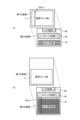
- FIG. 4A is a diagram showing an example in which the imaging device 1004 according to each embodiment is formed by a laminated CIS having a two-layer structure.
- the pixel section 2010 is formed in the semiconductor chip of the first layer
- the memory+logic section 2011 is formed in the semiconductor chip of the second layer.
- the pixel section 2010 includes at least the pixel array section 11 .
- the memory+logic unit 2011 includes, for example, the vertical scanning circuit 12, the timing control unit 13, the DAC 14, the column signal processing unit 15, the horizontal scanning circuit 16, and an interface for communicating between the imaging device 1004 and the outside. be able to.
- the memory+logic unit 2011 can also include a memory that stores pixel data output from the column signal processing unit 15, for example.
- the imaging device 1004 is configured as one solid-state imaging element 2000a by bonding the semiconductor chips of the first layer and the semiconductor chips of the second layer while electrically contacting them. .
- the imaging device 1004 can be formed with a three-layer structure in which semiconductor chips are stacked in three layers.
- FIG. 4B is a diagram showing an example in which the imaging device 1004 according to each embodiment is formed by a laminated CIS having a three-layer structure.
- the pixel section 2010 is formed in the semiconductor chip of the first layer
- the memory section 2012 is formed in the semiconductor chip of the second layer
- the logic section 2011' is formed in the semiconductor chip of the third layer.
- the logic unit 2011' includes the vertical scanning circuit 12, the timing control unit 13, the DAC 14, the column signal processing unit 15, the horizontal scanning circuit 16, and an interface for communicating between the imaging device 1004 and the outside. be able to.
- the memory unit 2012 can also include a memory that stores pixel data output from the column signal processing unit 15, for example.
- the first layer semiconductor chip, the second layer semiconductor chip, and the third layer semiconductor chip are bonded together while being in electrical contact with each other, whereby the imaging device 1004 is integrated into one. It is configured as one solid-state imaging device 2000b.
- FIG. 5 is a schematic diagram showing the structure of an example of the imaging device 1004 according to the embodiment.
- the imaging device 1004 employs the two-layer solid-state imaging device 2000a described with reference to FIG. 4A.
- a photoelectric conversion element is formed in the first layer 2010a of the substrate, and a pixel circuit that converts charges generated by the photoelectric conversion element into pixel signals and outputs them is the first layer of the substrate. It is formed in two layers 2010b.
- a pixel portion 2010 is composed of the first layer 2010a and the second layer 2010b.
- photoelectric conversion units 100 including photoelectric conversion elements and transistors for controlling readout of charges from the photoelectric conversion elements are arranged in a matrix on the first layer 2010a.
- circuit units 101 including pixel circuits that convert charges read from the photoelectric conversion units 100 into pixel signals are arranged in rows and columns corresponding to the photoelectric conversion units 100 in the first layer 2010a. Arranged in an array. More specifically, the circuit unit 101 is in electrical contact between the first layer 2010a and the second layer 2010b in a one-to-one relationship with the photoelectric conversion unit 100 corresponding in position on the first layer 2010a. It is placed while
- the circuit section 101 further includes part of the comparator 20 . That is, in each embodiment, the comparator 20 includes at least a first circuit (denoted as CMP(1)) to which a pixel signal is directly supplied from the pixel circuit, and a first circuit to which the output of the first circuit is supplied. 2 circuits (denoted as CMP(2) and (3)).
- the first circuit includes, for example, a circuit that compares the pixel signal output from the pixel circuit and the RAMP signal supplied from the DAC 14 .
- a vertical scanning circuit 12 a counter 30, a logic circuit 40, a peripheral circuit 50, and an interface circuit 60 (also referred to as an IF circuit in the figure) are arranged for the memory+logic unit 2011. .
- the peripheral circuit 50 includes the DAC 14.
- the interface circuit 60 is an interface for transmitting and receiving signals between the imaging device 1004 as the solid-state imaging device 2000a and the outside.
- the vertical scanning circuit 12 is arranged along the column direction of the pixel array section 11 at one end in the row direction of the memory+logic section 2011 (the right end in the example shown).
- the interface circuit 60 is arranged along the column direction of the pixel array section 11 at the other end (the left end in the drawing) of the memory+logic section 2011 in the row direction.
- a second circuit 210 obtained by dividing the comparator 20 is arranged for the memory+logic unit 2011 .
- the second circuits 210 are arranged along the row direction of the memory+logic unit 2011 at one end and the other end in the column direction (upper and lower ends in the example of FIG. 5).
- the second circuit 210 is provided for each column in the pixel array section 11 .
- the second circuits 210 are provided at both ends of the memory+logic section 2011 in the column direction along the row direction in the pixel array section 11 .
- the second circuit 210 is shared by a plurality of circuit units 101 arranged along columns in the second layer 2010b.
- each second circuit 210 arranged at one end (for example, the upper end in the drawing) of the memory+logic unit 2011 in the column direction is one of the circuit units 101 arranged in the second layer 2010b. It is shared by each circuit section 101 arranged in one end side half (the upper half in the example of FIG. 5).
- each second circuit 210 arranged at the other end in the column direction of the memory+logic unit 2011 for example, the lower end in FIG. Of these, it is shared by each circuit section 101 arranged in the other half (lower half in the example of FIG. 5).
- Each pixel 10 (each photoelectric conversion unit 100 and each circuit unit 101) is scanned in the column direction, that is, in the vertical direction, as indicated by arrows.
- the output from each pixel 10 (each circuit section 101) is transferred to the memory+logic section 2011 for each row.
- FIG. 6 is a schematic diagram for explaining a path for converting an analog pixel signal into a digital pixel signal (pixel data) and supplying it to the interface circuit 60. As shown in FIG. 6
- FIG. 6 is a diagram for explanation, and the arrangement of the logic circuit 40, the interface circuit 60, and the ADC (Analog to Digital Converter) 70 does not necessarily match the arrangement explained using FIG. not That is, in sections (a) and (b), the pixel array section 11 is provided on the first substrate, and the logic circuit 40, the interface circuit 60 and the ADC 70 are provided on the second substrate. It is also assumed that ADC 70 includes comparator 20 and counter 30 of FIG. That is, an analog pixel signal output from each pixel included in the pixel array section 11 is converted into pixel data by the ADC 70 and output to the outside via the logic circuit 40 and the interface circuit 60 .
- ADC 70 Analog to Digital Converter
- Section (a) of FIG. 6 is an example in which the ADCs 70 are arranged for each column. Also, section (b) is an example in which the ADC 70 is arranged for each pixel, and corresponds to each embodiment of the present disclosure.
- each ADC 70 is arranged on one end side in the column direction, and the interface circuit 60 is arranged on the other end side in the column direction.
- a pixel signal output from each pixel included in the pixel array section 11 is transferred to the end of the pixel section 2010 on the ADC 70 side via the vertical signal line VSL for each column, and is transmitted between the pixel section 2010 and the memory+logic section 2011. is supplied to each ADC 70 through the connection of .
- the pixel data output from each ADC 70 is supplied to the interface circuit 60 via the logic circuit 40, for example.
- each ADC 70 is arranged in a matrix in a region corresponding to the pixel array section 11, corresponding to each pixel arranged in the pixel array section 11. is placed in Each pixel included in the pixel array section 11 and each ADC 70 are connected to each other through a connection section provided in each ADC 70 between the first substrate and the second substrate. A pixel signal output from each pixel is converted into pixel data by the corresponding ADC 70 and supplied to the interface circuit 60 .
- the pixel signal output from each pixel extends from one end of the pixel array section 11 in the column direction (vertical direction) to the other end. Distance will be transferred.
- the pixel signal output from each pixel is transferred from the pixel section 2010 to the second substrate in the shortest possible time.
- the pixel data output from each ADC 70 is transferred over a maximum distance corresponding to the distance from one end to the other end in the column direction of the pixel array section 11, as indicated by the signal SGLb.
- the example shown in section (a) of FIG. 6 is an analog signal SGLa, which has a wide band and is susceptible to noise.
- the signal passing through the long-distance wiring is the digital signal SGLb, which has a narrower band and is less susceptible to noise than the analog signal SGLa.
- FIG. 7 is a schematic diagram schematically showing signal processing for pixel signals according to each embodiment.
- comparator 20 is divided into multiple circuits.
- the comparator 20 is divided into three circuits, a first-stage comparator 201, a middle-stage comparator 202, and a rear-stage comparator 203.
- the first-stage comparator 201 corresponds to the first circuit described using FIG.
- the middle-stage comparator 202 and the rear-stage comparator 203 correspond to the second circuit described using FIG. 5, and compare the output of the first circuit with the threshold.
- the middle stage comparator 202 and the rear stage comparator 203 can also be configured as one circuit.
- the long-distance wiring described using section (a) of FIG. the long-distance wiring is arranged at the boundary C between the counter 30 and the logic circuit 40 .
- the long-distance wiring is arranged at the boundary B between the first-stage comparator 201 and the middle-stage comparator 202, as described using section (b) of FIG.
- FIG. 8 is a schematic diagram showing an example in which the pixel array section 11 is vertically divided into a plurality of regions.
- the pixel array section 11 is vertically divided into four areas: pixel areas 11Up1 and 11Up2 , and pixel areas 11Dwn1 and 11Dwn2 .
- pixel regions 11Up1 and 11Up2 are the upper first and second pixel regions, respectively
- pixel regions 11Dwn1 and 11Dwn2 are the lower first and second pixel regions, respectively.
- an analog circuit 80Up1 and a logic circuit 40Up1 are arranged at a position corresponding to the pixel region 11Up1
- an analog circuit 80Up2 and a logic circuit 40Up2 are arranged at a position corresponding to the pixel region 11Up2.
- an analog circuit 80Dwn1 and a logic circuit 40Dwn1 are arranged at a position corresponding to the pixel region 11Dwn1
- an analog circuit 80Up2 and a logic circuit 40Dwn2 are arranged at a position corresponding to the pixel region 11Up2 .
- analog circuits 80Up 1 , 80Up 2 , 80Dwn 1 and 80Dwn 2 each include, for example, a pixel circuit, a comparator 20 and a counter 30 .
- a pixel signal output from each pixel in the pixel region 11Up1 is transferred row by row from the end of the pixel region 11Up1 to the memory+logic unit 2011 via the vertical signal line in the pixel region 11Up1, and is transferred to the analog circuit 80Up. 1 is entered.
- the output of the analog circuit 80Up1 is input to the logic circuit 40Up1 .
- the pixel signal output from each pixel is transferred over a distance that is at most 1/4 of the distance between both ends of the pixel array section 11 in the column direction. Shortened for the transfer distances described. However, there is no change from the existing configuration in that pixel signals are transferred via vertical signal lines. Therefore, the parasitic capacitance of the shortened vertical signal line affects only the settling in the pixels 10, and it is difficult to improve the characteristics such as the influence of noise.
- the distance over which the charge generated in the pixel 10 is transferred to the first-stage comparator 201 is extremely short, so the settling time in the pixel 10 can be shortened. Therefore, it is possible to speed up the readout time of charges from the pixels 10 . Further, since the vertical signal line, which is a heavy load, is connected to the output side of the first-stage comparator 201, the bandwidth of the signal transferred to the vertical signal line can be narrowed, and noise can be reduced.
- FIG. 9 is a circuit diagram showing an example configuration according to the first embodiment.
- each drive control signal for driving each pixel 10 supplied from the vertical scanning circuit 12 to each photoelectric conversion unit 100 and circuit unit 101 is omitted to avoid complexity.
- the photoelectric conversion unit 100 is configured in the first layer 2010a of the pixel unit 2010.
- the photoelectric conversion element 300 which is a photodiode; 302 and.
- the photoelectric conversion element 300 generates and accumulates charges according to the received light.
- the drain of the nMOS transistor 301 is connected to the cathode of the photoelectric conversion element 300 .
- the nMOS transistor 301 has its gate controlled to be non-conducting/conducting according to a signal TRG supplied from the vertical scanning circuit 12 . When the nMOS transistor 301 is in a conducting state, the charges accumulated in the photoelectric conversion element 300 are read out.
- the source of the nMOS transistor 301 is connected to the circuit section 101 corresponding to the photoelectric conversion section 100 from the first layer 2010a through the connection section 400 to the second layer 2010b.
- the connecting portion 400 can be a Cu--Cu direct bonding for directly bonding Cu electrodes, a through silicon via (TSV), a bonding portion composed of a microbump, or the like.
- the nMOS transistor 302 has a drain connected to the power supply line, a source connected to the cathode of the photoelectric conversion element 300 together with the drain of the nMOS transistor 301 , and a non-conducting/conducting state by a signal OFG supplied from the vertical scanning circuit 12 to the gate. controlled.
- the nMOS transistor 302 is in a conductive state, the charges accumulated in the photoelectric conversion element 300 are extracted to, for example, the power supply line.
- the circuit portion 101 is formed in the second layer 2010b of the pixel portion 2010.
- FIG. The circuit section 101 includes a differential pair using nMOS transistors 311a and 311b, pMOS transistors 310a and 310b which are p-channel MOS transistors forming a current mirror circuit, and an nMOS transistor 312 as a current source.
- the sources of pMOS transistors 310a and 310b are each connected to power supply line VDD1 .
- connection point 304 where the connection section 400 for connecting to the photoelectric conversion section 100 and the gate of the nMOS transistor 311b are connected is a floating diffusion layer (FD).
- the connection point 304 is further connected to the source of the nMOS transistor 303 .
- the drain of the nMOS transistor 303 is connected to the connection point where the drain of the nMOS transistor 311b and the drain of the pMOS transistor 310b are connected.
- the non-conducting/conducting state of the nMOS transistor 303 is controlled according to the signal RST supplied from the vertical scanning circuit 12 .
- circuit unit 101 can share an FD among a plurality of circuit units 101 adjacent to each other.
- an FD can be shared by four circuit units 101 (pixels 10) adjacent to each other.
- the nMOS transistor 303 With the nMOS transistor 303 in a conductive state, the charge in the FD is drawn to the power supply line VDD1 through the pMOS transistor 310b, and the FD is reset.
- the nMOS transistor 301 When the nMOS transistor 301 is in a conducting state, the charge accumulated in the photoelectric conversion element 300 is transferred to the FD and accumulated.
- FD is connected to the gate of nMOS transistor 311b.
- the charge accumulated in the FD is converted into a voltage when read out from the FD, and supplied as a pixel signal to the gate of the nMOS transistor 311b.
- the nMOS transistor 303 and the FD constitute a pixel circuit that outputs a pixel signal based on the charges generated by the photoelectric conversion element 300 .
- the FD functions as a charge-voltage converter that converts the charge generated by the photoelectric conversion element 300 into a voltage.
- a gate of the nMOS transistor 311a is connected to a RAMP wiring 330 to which a RAMP signal (reference signal) generated by the DAC 14 is transmitted.
- a RAMP signal generated by the DAC 14 is supplied to the vertical scanning circuit 12 .
- the vertical scanning circuit 12 outputs a RAMP signal to the RAMP wiring 330 via the connection section 401 for each row of the matrix arrangement of the circuit section 101 .
- the connecting portion 401 can be a Cu--Cu direct bonding for directly bonding Cu electrodes, a Through Silicon Via (TSV), or a bonding portion composed of a microbump or the like.
- the differential pair compares the RAMP signal supplied to the gate of the nMOS transistor 311a with the pixel signal supplied to the gate of the nMOS transistor 311b.
- the result of the comparison by the operating pair is output as the voltage difference between the two from the connection point where the drain of the pMOS transistor 310b and the drain of the nMOS transistor 311b are connected.
- This differential voltage is supplied to the vertical signal line VSL via the switch circuit 327 .
- the switch circuit 327 is a row selection switch whose non-conducting/conducting state is controlled for each row according to a drive signal output from the vertical scanning circuit 12, for example.
- the vertical signal line VSL is connected to the second circuit 210 configured in the memory+logic section 2011 from the second layer 2010b through the connection section 402 such as a Cu--Cu bond.
- the connecting portion 402 can be a Cu--Cu direct bonding for directly bonding Cu electrodes, a Through Silicon Via (TSV), or a bonding portion composed of a microbump or the like.
- the second circuit 210 is provided for each column of the pixels 10 arranged in the pixel array section 11 .
- the second circuit 210 includes pMOS transistors 320 , 322 , 323 and 325 and nMOS transistors 321 , 324 and 326 .
- a connection portion 402 is connected to the gate of the pMOS transistor 320 and receives a signal from the vertical signal line VSL.
- the pMOS transistor 320 has a source connected to the power supply line VDD 1 and a drain connected to the drain of the nMOS transistor 321 .
- the gate of nMOS transistor 321 is connected to bias voltage V BIAS .
- the pMOS transistors 322, 323 and 325 and the nMOS transistors 324 and 326 form a positive feedback circuit.
- This positive feedback circuit is driven by a power supply on power supply line VDD2 whose voltage is lower than power supply line VDD1 on which the differential pair is driven.
- the pMOS transistor 320 and the nMOS transistor 321 form a voltage conversion circuit that converts the output from the differential pair into a low voltage signal that allows the positive feedback circuit to operate.
- the bias voltage V BIAS may be any voltage that can be converted into a voltage that does not destroy each transistor of the positive feedback circuit that operates at a low voltage.
- the bias voltage VBIAS can be the same voltage as the voltage of the power supply line VDD2 that drives the positive feedback circuit.
- the positive feedback circuit outputs a comparison result signal that is inverted when the level of the pixel signal is higher than the level of the reference signal (RAMP signal) based on the signal obtained by converting the output signal from the differential pair to a low voltage.
- This positive feedback circuit speeds up the transition speed when the output signal OUT output as the comparison result signal is inverted.
- the source of the nMOS transistor 321 which is the output end of the voltage conversion circuit, is connected to the drains of the pMOS transistor 323 and the nMOS transistor 324, and the gates of the pMOS transistor 325 and the nMOS transistor 326.
- the sources of pMOS transistors 322 and 325 are connected to power supply line VDD2
- the drain of pMOS transistor 322 is connected to the source of pMOS transistor 323, and the gate of pMOS transistor 323 is the output end of this positive feedback circuit. It is connected to the drains of transistor 325 and nMOS transistor 326 .
- the sources of nMOS transistors 324 and 326 are connected to a predetermined voltage, eg, ground potential.
- An initialization signal INI is supplied to the gates of the pMOS transistor 322 and the nMOS transistor 324, respectively.
- the pMOS transistor 325 and the nMOS transistor 326 constitute an inverter circuit, and the connection point between their drains is the output terminal from which the second circuit 210 outputs the output signal OUT.
- the charge generated by the photoelectric conversion element 300 in the photoelectric conversion unit 100 is integrated with the first layer 2010a on which the photoelectric conversion unit 100 is provided. It is provided in the second layer 2010b and transferred to the circuit section 101 corresponding to the photoelectric conversion section 100 in position.
- the circuit unit 101 converts analog pixel signals based on charges transferred from the photoelectric conversion unit 100 into digital pixel signals (pixel data) and outputs the digital pixel signals (pixel data). According to this configuration, the charge read from the photoelectric conversion unit 100 is transferred to the circuit unit 101 over a very short distance, so that the influence of noise during charge transfer can be suppressed.
- Focal plane distortion (Regarding focal plane distortion) Focal plane distortion according to the first embodiment will be described.
- the exposure of the photoelectric conversion elements 300 is performed row by row, so the exposure timing of each row is different in the vertical direction (column direction), and so-called focal plane distortion may occur in the captured image.
- FIG. 10A is a schematic diagram for explaining focal plane distortion when the pixel array section 11 is vertically divided into two.
- ADCs (Analog to Digital Converters) 70Up and 70Dwn include a comparator 20 and a counter 30, respectively. Also, the configurations of the logic circuit 40 and the interface circuit 60 are omitted.
- Section (a) of FIG. 10A shows an example in which the pixel array section 11 is divided into a pixel region 11Up and a pixel region 11Dwn.
- the vertical signal line VSL is divided by the boundary region 150a between the pixel region 11Up and the pixel region 11Dwn. It is supplied from the first layer 2010a to the second layer 2010b.
- Section (b) of FIG. 10A shows an example of arrangement of ADCs 70Up and 70Dwn corresponding to pixel regions 11Up and 11Dwn in the second layer 2010b.
- ADCs 70Up and 70Dwn are provided on both sides of boundary region 150b corresponding to boundary region 150a in first layer 2010a. Note that the ADCs 70Up and 70Dwn are provided for each vertical signal line VSL.
- an analog pixel signal output from each pixel included in the pixel array section 11 is converted into pixel data by the ADC 70 and output to the outside via the logic circuit 40 and the interface circuit 60 (not shown).
- the vertical signal line VSL is connected to the corresponding ADCs 70Up and 70Dwn from the boundary region 150a where the vertical signal line VSL is divided in the first layer 2010a through the boundary region 150b of the second layer 2010b.
- FIG. 10B is a schematic diagram for explaining focal plane distortion in the configuration according to the first embodiment.
- FIG. 10B is a diagram for explanation, and configurations such as the logic circuit 40 and the interface circuit 60 are omitted.
- the pixel array section 11 includes N rows in a matrix arrangement in which the photoelectric conversion sections 100 and the circuit section 101 are arranged. That is, the pixel array section 11 includes N pixels 10 in the column direction. Note that when the FD is shared by a plurality of circuit units 101, the value N is used as the FD sharing unit.
- each photoelectric conversion unit 100 provided on the first layer 2010a includes the first-stage comparator 201 (first circuit) in the comparator 20 . Therefore, the pixel array section 11 can be regarded as being divided into rows in the column direction, and the vertical signal lines VSL are arranged in the boundary regions 150 1 , 150 2 , . It can be considered to be N-divided.
- Section (b) of FIG. 10B shows an example of placement of ADCs 71 1 , 71 2 , . . . , 71 N in the second layer 2010b.
- Each ADC 71 1 , 71 2 , . and a comparison process with a reference signal are identical to each ADC 71 1 , 71 2 , . and a comparison process with a reference signal.
- the longest vertical signal line VSL is half the length of the pixel array section 11 in the vertical direction.
- the length of wiring or connection corresponding to the vertical signal line VSL is the length in the direction perpendicular to the substrate surface from the first layer 2010a to the second layer 2010b, which is extremely short compared to the case of FIG. 10A. , it is possible to further suppress the influence of noise.
- the second layer 2010b may be filled with ADCs 71 1 , 71 2 , . Therefore, it is preferable to arrange the logic circuit 40 and the interface circuit 60 in the memory+logic unit 2011 as shown in section (c) of FIG. 10C.
- sections (a) and (b) of FIG. 10C are common to sections (a) and (b) of FIG. 10B, so description thereof will be omitted here.
- the comparator 20 and the counter 30 can be configured for each pixel 10, operation as a global shutter becomes possible. However, especially in cameras for mobile use, it is difficult to configure the comparator 20 and the counter 30 for each pixel 10 because the pixel cell size must be small.
- FIG. 11 is a schematic diagram showing an arrangement example of the RAMP wiring and each connection portion according to the first embodiment.
- the circuit section 101 is arranged in a matrix pattern corresponding to each photoelectric conversion section 100 in the pixel array section 11 of the first layer 2010a.
- the connection section 402 connects the vertical signal lines VSL provided for each column on the second substrate and the second circuits 210 provided for each column on the memory+logic section 2011. do.
- the connection portions 402 are provided at both ends of each column in the arrangement of the second circuits 210 in the second layer 2010b.
- a RAMP wiring 330 for supplying a RAMP signal to the circuit section 101 is provided for each row in the matrix arrangement of the circuit section 101 on the second layer 2010b.
- One end of each RAMP wiring 330 (the right end in the example of the drawing) is connected to the connection portion 401 .
- the vertical scanning circuit 12 is provided at one end (the right end in the example shown) in the horizontal direction of the substrate (corresponding to the row direction in the matrix arrangement of the circuit units 101). Further, an interface circuit 60 is provided on the other horizontal end side of the substrate.
- a second circuit 210, a counter 30, and a logic circuit 40 are provided in a region between the vertical scanning circuit 12 and the interface circuit 60 corresponding to, for example, the matrix arrangement of the circuit unit 101. , DAC 14 are arranged.
- the logic circuit 40 is arranged on the interface circuit 60 side (left side) and the DAC 14 is arranged on the vertical scanning circuit 12 side (right side) with respect to the vertical central portion of the area.
- Counters 30 are arranged on both sides of the central portion in the vertical direction according to each column of the matrix arrangement of the circuit portions 101 . Further outside the counter 30, a second circuit 210 is arranged according to each column. In the example of the figure, each counter 30 and each second circuit 210 corresponding to each column are shown as one block.
- connection portion 402 is provided at each end portion of each second circuit 210 corresponding to each side of the memory+logic portion 2011 in the vertical direction.
- a signal output from each circuit unit 101 to the vertical signal line VSL in the second layer 2010 b is supplied to each second circuit 210 via each connection unit 402 .
- a RAMP signal generated by the DAC 14 is supplied to the vertical scanning circuit 12 via the wiring 331 .
- the vertical scanning circuit 12 outputs the RAMP signal supplied from the DAC 14 to each connection section 401 provided for each row of the matrix arrangement of the circuit section 101 .
- the RAMP signal is transferred from the memory+logic section 2011 to the second layer 2010b via each connection section 401 and supplied to the circuit section 101 row by row.
- the first circuit that compares the pixel signal and the RAMP signal corresponding to the first-stage comparator 201 includes: This is an example of connecting a latch circuit that latches a comparison result.
- FIG. 12A is a schematic diagram for explaining an example of performing an operation corresponding to the global shutter method in the configuration of the first modified example of the first embodiment.
- a first substrate is provided with a pixel array section 11 in which photoelectric conversion sections 100 are arranged in a matrix.
- four photoelectric conversion units 100 adjacent to each other share an FD to which charges generated by the photoelectric conversion elements 300 are transferred.
- one FD is shared by four photoelectric conversion units 100 numbered (1) to (4).
- the four photoelectric conversion units 100 of the FD sharing unit are exposed in order of numbers (1) to (4), for example.
- an ADC 72 is arranged on the second substrate for each FD sharing unit.
- Each ADC 72 includes a first circuit 73 including a circuit that compares the pixel signal and the RAMP signal, and a latch circuit 74 that latches the output of the first circuit 73 .
- the first circuit 73 can correspond to, for example, the circuit section 101 described above.
- the imaging device 1004 simultaneously exposes each of the photoelectric conversion units 100 numbered (1), for example.
- the charge generated in each photoelectric conversion unit 100 by exposure is transferred to the FD, converted into a voltage, and supplied to each ADC 72 as a pixel signal.
- the supplied pixel signal is compared with the RAMP signal in the first circuit 73 and the comparison result is latched in the latch circuit 74 .
- the comparison result latched by each latch circuit 74 is read from the latch circuit 74 row by row, converted into pixel data by the second circuit 210 (not shown), and output to the outside through the logic circuit 40 and the interface circuit 60. be done.
- the imaging device 1004 corresponds to the global shutter method. operation becomes possible.
- FIG. 12B is a schematic diagram for explaining an example of a rolling shutter operation in the configuration of the first modified example of the first embodiment, similar to FIG. 12A.
- the configurations of the first substrate and the second substrate are the same as those shown in FIG. 12A, so detailed description thereof will be omitted here.
- rows and columns are defined according to FD sharing units. That is, on the second substrate, the ADCs 72 are arranged in an array of 4 rows ⁇ 6 columns. Also, each line shall be the first line, the second line, . . . from the bottom to the top of the drawing.
- the imaging device 1004 simultaneously performs exposure in each photoelectric conversion unit 100 of number (1) in the FD sharing unit corresponding to each ADC 72 in the first row, for example.
- the charge generated in each photoelectric conversion unit 100 by exposure is transferred to the FD, converted into a voltage, and supplied as a pixel signal to each ADC 72 in the first row.
- the supplied pixel signal is compared with the RAMP signal in the first circuit 73 and the comparison result is latched in the latch circuit 74 .
- the comparison result latched from the latch circuit 74 is read out, converted into pixel data by the second circuit 210 (not shown), and output to the outside via the logic circuit 40 and the interface circuit 60 .
- This operation is sequentially performed for each photoelectric conversion unit 100 numbered (1) to (4) included in the FD sharing unit corresponding to each ADC 72 in the first row, and as described above, each charge is converted to a voltage. , and generates pixel data based on voltage.
- the photoelectric conversion units 100 with numbers (1) to (4) is completed, next, the photoelectric conversion units with numbers (5) to (8) included in the FD sharing units corresponding to the ADCs 72 in the second row are exposed.
- the above-described operations are sequentially performed in the same manner.
- a rolling shutter operation can be performed by sequentially performing this operation on the third line, the fourth line, and so on.
- the latch operation by the latch circuit 74 or the latch circuit 74 itself can be omitted.
- a second modification of the first embodiment is an example in which the configurations of the second layer and the memory+logic section 2011 according to the first embodiment shown in FIGS. 5 and 11 are changed.
- FIG. 13 is a schematic diagram showing an example configuration of an imaging device 1004 according to the second modification of the first embodiment.
- the imaging device 1004 employs the two-layer solid-state imaging device 2000a described with reference to FIG. 4A.
- the configuration according to the second modification of the first embodiment will be described in comparison with the configurations of FIGS. 5 and 11 according to the first embodiment.
- the vertical scanning circuit 12 is arranged in the memory+logic section 2011.
- the vertical scanning circuit 12 is divided into two parts, a vertical scanning circuit 12L and a vertical scanning circuit 12H. Also referred to as vertical scanning circuit L and vertical scanning circuit H respectively).
- the vertical scanning circuit 12L is arranged in the memory+logic section 2011, and the vertical scanning circuit 12H is arranged in the second layer 2010b.
- the vertical scanning circuits 12L and 12H drive the photoelectric conversion sections 100 and the circuit sections 101 in one and the other regions obtained by dividing the pixel array section 11 in the column direction, respectively.
- the second circuits 210 of each column are arranged in the memory+logic unit 2011 .
- the second circuits 210 in each column are arranged on the second layer 2010b. More specifically, the second circuits 210 are arranged at the upper and lower ends in the column direction of the circuit units 101 arranged in a matrix on the second layer 2010b.
- Each of the second circuits 210 is connected to each of the counters 30 arranged on the upper and lower ends of the memory+logic section 2011 in the column direction via a connecting section 402' such as a Cu--Cu bond.
- FIGS. 5 and 11 Which of the configuration according to the first embodiment shown in FIGS. 5 and 11 and the configuration according to the second modification of the first embodiment shown in FIG. It can be determined according to the state of each chip. For example, when a large area is required for the pixel section 2010 (first layer 2010a and second layer 2010b), the configurations of FIGS. 5 and 11 are adopted so that many circuits can be arranged in the memory+logic section 2011. . Further, for example, in the memory+logic unit 2011, if the logic circuit 40 or the like needs a large area, the configuration of FIG. Deploy. By changing these arrangements, it may be possible to reduce the overall size of the imaging device 1004, that is, the solid-state imaging device 2000a.
- the vertical scanning circuit 12 is divided into two vertical scanning circuits 12L and 12H, which are arranged in the memory+logic section 2011 and the second layer 2010b, respectively, and the second circuit 210 is arranged in the second layer 2010b.
- the vertical scanning circuit 12 may not be divided and the second circuit 210 may be placed on the second layer 2010b.
- the second circuit 210 is arranged in the memory+logic section 2011, and the vertical scanning circuit 12 is divided into two vertical scanning circuits 12L and 12H, which are arranged in the memory+logic section 2011 and the second layer 2010b, respectively. good too.
- the vertical scanning circuit 12 may be arranged on the second layer 2010b, and in addition to the second circuit 210, the counter 30 may also be arranged on the second layer 2010b.
- FIG. 14 is a schematic diagram for explaining the configuration according to the third modification of the first embodiment.
- the first stage comparator 201 and the middle stage comparator 202 are also indicated as "1st" and "2nd", respectively.
- one middle-stage comparator 202 is arranged for each column in the pixel array section 11, as shown in section (a) of FIG. That is, the output of each first stage comparator 201 arranged along the column of the pixel array section 11 is input to one middle stage comparator 202 arranged in the column.
- the output of the first-stage comparators 201 arranged in odd-numbered rows is transferred to the first middle-stage comparator 202 1 . to enter. Also, the output of the first-stage comparator 201 arranged in the even-numbered row is input to the second middle-stage comparator 202 2 .
- the first-stage comparator 201 and the middle-stage comparator 202 (the second middle-stage comparators 202 1 and 202 2 ) in this way, it is possible to simultaneously read out the output of the first-stage comparator 201 by multiple lines (two lines in this example). and can operate at higher speeds.
- the second embodiment is an example in which the configuration of the circuit section 101 that compares the RAMP signal and the pixel signal is different from that of the circuit section 101 in the first embodiment.
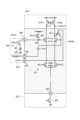
- FIG. 15 is a circuit diagram showing an example configuration according to the second embodiment.
- each drive control signal for driving each pixel 10 supplied from the vertical scanning circuit 12 to each photoelectric conversion unit 100 and circuit unit 101 is omitted to avoid complexity.
- the pixel circuit that drives the photoelectric conversion element 300 and outputs the pixel signal includes four nMOS transistors 301 , 303 , 305 and 306 .
- the nMOS transistor 301 has a source connected to the cathode of the photoelectric conversion element 300 and a drain connected to the source of the nMOS transistor 303 and the gate of the nMOS transistor 305 via the connection portion 400 .
- the nMOS transistor 301 is controlled to be non-conducting/conducting according to a signal TRG supplied to its gate from the vertical scanning circuit 12 .
- a photoelectric conversion unit 100 is configured including an nMOS transistor 301 and a photoelectric conversion element 300 .
- a connection point 304 where the drain of the nMOS transistor 301, the source of the nMOS transistor 303, and the gate of the nMOS transistor 305 are connected is FD.
- the nMOS transistor 301 is in a conducting state, the charge accumulated in the photoelectric conversion element 300 is transferred to the FD.
- the drain of the nMOS transistor 303 is connected to the power supply line, and the non-conducting/conducting state is controlled according to the signal RST supplied to the gate from the vertical scanning circuit 12 .
- the nMOS transistor 303 is in a conductive state, the charges accumulated in the FD are drawn to the power supply line, and the FD is reset.
- the nMOS transistor 305 has a drain connected to the power supply line and a source connected to the drain of the nMOS transistor 306 .
- the source of nMOS transistor 306 is connected to the sources of pMOS transistors 340 and 353 .
- the nMOS transistor 306 is controlled to be non-conducting/conducting according to a signal SEL supplied to its gate from the vertical scanning circuit 12 .
- a signal SEL is a row selection signal for selecting a pixel circuit that outputs a signal to the vertical signal line VSL for each row, and the nMOS transistor 306 functions as a row selection transistor that performs row selection.
- the nMOS transistor 306 In response to the signal SEL, the nMOS transistor 306 is in a conducting state, and charges are read out from the FD, converted into voltages, and used as pixel signals.
- This pixel signal is amplified by the nMOS transistor 305 and input to the sources of the pMOS transistors 340 and 353 via the nMOS transistor 306 .
- the nMOS transistor 305 functions as an amplification transistor that amplifies the pixel signal.
- the gate of pMOS transistor 340 is connected to RAMP wiring 330 via capacitor 352 .
- a switch circuit 341 is connected between the gate and drain of the pMOS transistor 340 .
- the switch circuit 341 is controlled to be non-conducting/conducting according to an auto-zero signal (AZ signal) supplied from the vertical scanning circuit 12 .
- a first circuit corresponding to the first-stage comparator 201 is configured including the pMOS transistor 340 and the switch circuit 341 .
- the pMOS transistor 353 has its gate and drain connected and functions as a clamp circuit for the pMOS transistor 340 .
- the drain of the pMOS transistor 353 is connected to the drain of the pMOS transistor 340, and the drain of the pMOS transistor 340 is connected to the vertical signal line VSL.
- a capacitor 354 connected to the vertical signal line VSL is a parasitic capacitance of the vertical signal line VSL.
- the vertical signal line VSL is connected to the current source 355 via the connection portion 402 .
- Current source 355 is realized by, for example, an nMOS transistor.
- An output from the circuit section 101 including the nMOS transistor 306 which is rendered conductive in response to the signal SEL is taken out from the connection point where the connection section 402 and the current source 355 are connected. This extracted output is supplied to a second circuit 210 (shown as CMP(2),(3) in the figure).
- the photoelectric conversion section 100 is provided on the first layer 2010a in the solid-state imaging device 2000a.
- Circuit portion 101 includes nMOS transistors 303, 305 and 306, pMOS transistors 340 and 353, and capacitor 352, and is provided in second layer 2010b.
- the current source 355 , the second circuit 210 (not shown), and the like are provided in the memory+logic section 2011 .
- FIG. 16 is a timing chart showing an example of variations in input/output signals relating to the circuit section 101 according to the second embodiment.
- an input voltage V VSL indicates a voltage input from the source of the nMOS transistor 306 to the source of the pMOS transistor 340 .
- a reference voltage V RMP indicates the voltage of the RAMP signal.
- the auto-zero signal AZ is input over a predetermined auto-zero period.
- the gate and drain of the pMOS transistor 340 are short-circuited, and an auto-zero operation as a comparator is performed.
- the DAC 14 gradually lowers the reference voltage V RMP based on the reference signal (RAMP signal) over a certain period from timing T2 .
- the nMOS transistors 301, 303, 305 and 306 and the FD pixel circuit are initialized, and the input voltage V VSL (that is, the reset level) at this time is V VSLp .
- Vdp be the drain voltage Vd of the pMOS transistor 340 at this timing T3 . If less than this Vdp is set to low level and Vdp or more is set to high level, the drain voltage Vd of the pMOS transistor 340 is inverted from low level to high level at timing T3 .
- the DAC 14 initializes the reference voltage and gradually lowers the reference voltage VRMP over a certain period from timing T5 .
- charge is transferred to the FD, and the input voltage V VSL (that is, the signal level) at this time is V VSLd .
- This signal level V VSLd is lower than the reset level V VSLp by ⁇ V.
- the reference voltage V RMP and the signal level V VSLd substantially match.
- the voltage drop amount ⁇ V of the input voltage V VSL is equal to that of the drain voltage Vd. It is the same as the amount of voltage drop.
- the inversion of the drain voltage Vd is performed based on the drain voltage Vdd obtained by dropping the voltage drop amount ⁇ V from the input voltage VVSL . It is conceivable to judge
- FIG. 17 is a circuit diagram showing an example configuration according to the existing technology.
- comparator 20 includes pMOS transistors 340 and 353, switch circuit 341 and capacitor 352 shown in FIG.
- Comparator 20 further includes a capacitor 360, a pMOS transistor 363, nMOS transistors 362 and 364 forming clamp circuits for the input and output of pMOS transistor 363, respectively, and a current source 355'.
- the pMOS transistor 363 functions as an output transistor for taking out the output of the comparator 20 .
- a pixel circuit including a photoelectric conversion element 300, nMOS transistors 301, 303, 305 and 306 for reading out charges from the photoelectric conversion element 300 and outputting a pixel signal, and an FD is a vertical signal.
- Multiple connections are made to the line VSL.
- Comparator 20 is shared by these multiple circuits. Further, the photoelectric conversion element 300 and the nMOS transistor 301 are provided on the first layer 2010a of the pixel section 2010, and the nMOS transistors 303, 305 and 306 and the FD among the pixel circuits are provided on the second layer 2010b. . It is also assumed that the comparator 20 is provided in the memory+logic unit 2011 .
- the band can be limited by the capacitor 354, which is the parasitic capacitance of the vertical signal line VSL. Therefore, noise can be reduced without adding the capacitor 360 to the memory+logic unit 2011 .
- a first modified example of the second embodiment is an example in which the positions of the row select transistors in the above-described second embodiment are changed.
- FIG. 18 is a circuit diagram showing an example configuration according to the first modification of the second embodiment.
- the first circuit including the pMOS transistor 340 and the switch circuit 341 corresponding to the first-stage comparator 201 is the output of the pixel circuit, that is, the It is connected to the source of nMOS transistor 306 which is a row select transistor.
- the source of the nMOS transistor 305 which is an amplification transistor, is connected to the source of the pMOS transistor 340, and the drain of the pMOS transistor 340 is connected to the drain of the nMOS transistor 306.
- the source of the nMOS transistor 306 is connected to the vertical signal line VSL.
- a vertical signal line VSL is connected to the drain of an nMOS transistor 307 as a current source via a connection portion 402 .
- An output OUT is taken out from a connection point where the connection portion 402 and the nMOS transistor 307 are connected. This output OUT is supplied to a second circuit 210 (not shown).
- the photoelectric conversion section 100 including the photoelectric conversion element 300 and the nMOS transistor 301 is provided in the first layer 2010 a of the pixel section 2010 .
- a circuit section 101 including a pixel circuit, a pMOS transistor 340 , a switch circuit 341 and a capacitor 342 is provided in the second layer 2010 b of the pixel section 2010 .
- an nMOS transistor 307 as a current source and a second circuit 210 are provided in the memory+logic portion 2011 .
- band limitation is possible due to the parasitic capacitance of the vertical signal line VSL. Therefore, noise can be reduced without adding a capacitor for limiting the band to the memory+logic unit 2011 .
- FIG. 19 is a schematic diagram showing an example in which the configuration according to the second embodiment shown in FIG. 18 is arranged in a matrix.
- a circuit 102 including a photoelectric conversion unit 100 and a circuit unit 101 is arranged in a matrix.
- the source of the row selection transistor whose gate receives the signal SEL is connected to the vertical signal line VS for each column of the matrix arrangement.
- Each vertical signal line VSL is connected to the drain of an nMOS transistor 307 as a current source via each connection portion 402 .
- An output OUT is taken out from each connection point where each connection portion 402 and the drain of each nMOS transistor 307 are connected.
- Each output OUT extracted from each vertical signal line VSL is supplied to a second circuit (not shown) for each column.
- the photoelectric conversion portion 100 is provided in the first layer 2010a of the pixel portion 2010, and the circuit portion 101 is provided in the second layer 2010b. be done.
- Each photoelectric conversion unit 100 is connected to the circuit unit 101 via a connection unit 400 .
- a memory+logic unit 2011 is provided with an nMOS transistor 307 as a current source for each column and a second circuit 210 (not shown). Each vertical signal line VSL is connected to the nMOS transistor 307 via a connection portion 402 . Although not shown, the RAMP wiring 330 for transmitting the RAMP signal output from the DAC 14 and the wiring for transmitting the auto-zero signal (AZ signal) supplied from the vertical scanning circuit 12 are connected to the respective memories.
- the + logic section 2011 is connected to the circuit 102 (circuit section 101 ) via the connection section 401 .
- FIG. 20 is a circuit diagram showing an example configuration according to a second modification of the second embodiment.
- a second modification of the second embodiment, as shown in FIG. 20, is the first circuit that compares the pixel signal and the RAMP signal, which was described with reference to FIG. 9 in the first embodiment.
- This is an example in which a switch circuit 341 that performs auto zero is added to the configuration using a differential pair.
- the switch circuit 341 is configured using pMOS transistors.
- the source of the pMOS transistor is connected to the connection point where the drain of one pMOS transistor 310b forming the current mirror circuit and the drain of the nMOS transistor 311b forming one of the differential pair are connected.
- an output OUT is extracted from the connection point and supplied to the second circuit 210 via a vertical signal line VSL (not shown).
- the drain of the pMOS transistor is connected to the gate of the nMOS transistor 311b and to the connection section 401 via the capacitor 342.
- a connection unit 401 is supplied with a RAMP signal output from a DAC 14 (not shown) provided in the memory+logic unit 2011 .
- the RAMP signal is supplied from connection 401 through capacitor 342 to the gate of nMOS transistor 311b and the drain of the pMOS transistor.
- a signal AZ for controlling the auto-zero operation is supplied to the gate of the pMOS transistor via a connection section 401 .
- the drains of nMOS transistors 306a and 306b are connected to the sources of nMOS transistors 311a and 311b forming a differential pair, respectively.
- the sources of nMOS transistors 306a and 306b are connected together, and the connection point is connected via connection 402 to the drain of nMOS transistor 307 as a current source.
- Signal SEL is supplied to the gates of nMOS transistors 306a and 306b. That is, nMOS transistors 306a and 306b function as select transistors.
- the photoelectric conversion section 100 including the photoelectric conversion element 300 and the nMOS transistor 301 is provided in the first layer 2010 a of the pixel section 2010 .
- a circuit section 101 using a differential pair of nMOS transistors 311 a and 311 b and an nMOS transistor 303 included in the pixel circuit are provided in the second layer 2010 b of the pixel section 2010 .
- Each photoelectric conversion unit 100 is connected to the circuit unit 101 via a connection unit 400 .
- a memory+logic unit 2011 is provided with pMOS transistors 310 a and 310 b that form a current mirror circuit, an nMOS transistor 307 as a current source, and a second circuit 210 (not shown).
- the RAMP wiring 330 for transmitting the RAMP signal output from the DAC 14 and the wiring for transmitting the auto-zero signal (AZ signal) supplied from the vertical scanning circuit 12 are connected to the respective memories.
- the + logic section 2011 is connected to the circuit section 101 via the connection section 401 .
- band limitation is possible due to the parasitic capacitance of the vertical signal line VSL. Therefore, noise can be reduced without adding a capacitor for limiting the band to the memory+logic unit 2011 .
- FIG. 21 is a circuit diagram showing an example configuration according to the third modification of the second embodiment.
- pMOS transistor 345 includes connections corresponding to pMOS transistor 340 of FIG.
- a switch circuit 341 whose non-conducting/conducting state is controlled by a signal AZ is connected between the gate and drain of the pMOS transistor 345 .
- the switch circuit 341 is configured using pMOS transistors.
- a capacitor 343 is further connected between the gate and drain of the pMOS transistor 345 . Further, to the gate of the pMOS transistor 345, one end of a capacitor 344 having the other end connected to a predetermined potential (for example, ground potential) is connected.
- a predetermined potential for example, ground potential
- the pMOS transistor 345 can function as an amplifier. Specifically, the pMOS transistor 340 amplifies the signal supplied from the source of the nMOS transistor 305 with an amplification factor n according to the capacitance ratio between the capacitors 343 and 342 and outputs the amplified signal from the drain.
- the vertical signal line VSL is connected to the drain of the nMOS transistor 307 of the current source via the connection portion 402 .
- the output OUT is taken out from the connection point where the connection portion 402 and the drain of the nMOS transistor 307 are connected.
- the output OUT is supplied to a comparator 20 (not shown).
- the photoelectric conversion section 100 including the photoelectric conversion element 300 and the nMOS transistor 301 is provided in the first layer 2010 a of the pixel section 2010 .
- the nMOS transistors 303, 305 and 306, FD (connection point 304), switch circuit 341 and pMOS transistor 345, and capacitors 343 and 344 included in the pixel circuit are provided in the second layer 2010b of the pixel section 2010.
- FIG. Each photoelectric conversion unit 100 is connected to the circuit unit 101 via a connection unit 400 .
- a memory+logic unit 2011 is provided with an nMOS transistor 307 as a current source and a comparator 20 (not shown). Although not shown, wiring for transmitting an auto-zero signal (AZ signal) supplied from the vertical scanning circuit 12 is connected from the memory+logic unit 2011 to the circuit unit 101 via the connection unit 401, respectively. be done.
- AZ signal auto-zero signal
- the pMOS transistor 345 does not function as the first-stage comparator 201, so the comparator 20 must be provided separately. Even in this case, the level of the signal output to the vertical signal line VSL is enhanced by setting the capacitances of the capacitors 343 and 342 so that the amplification factor n of the pMOS transistor 345 becomes n>1. It is possible to reduce noise relatively.
- the third embodiment is an example in which the RAMP signal is applied not to the gate of the pMOS transistor 340 but to the FD in the configuration described with reference to FIG.
- FIG. 22 is a schematic diagram showing an example configuration according to the third embodiment. Here, in order to avoid complication, detailed description of the parts common to FIG. 18 will be omitted.
- the capacitor 346 has one end connected to the FD (connection point 304 in this example) and the other end connected to the RAMP wiring 330 provided for each row.
- a RAMP signal connected from the DAC 14 is supplied to the connection section 401 via the row selection circuit 120 for each row.
- the row selection circuit 120 can employ a switch circuit whose non-conduction/conduction state is controlled by a row selection signal output from the vertical scanning circuit 12, for example.
- the RAMP signal supplied to the connection portion 401 is applied to the other end of the capacitor 346 via the RAMP wiring 330 provided for each row.
- the potential of the charges accumulated in the FD changes according to the RAMP signal applied to the capacitor 346 via the RAMP wiring 330. Therefore, the level of the voltage obtained by converting the charge read from the FD changes according to the change of the RAMP signal.
- FIG. 23 is an example timing chart for explaining the operation of the imaging device 1004 according to the third embodiment.
- FIG. 23 shows the timing relationship of the signal SEL driving the nMOS transistor 305, the signal RST driving the nMOS transistor 303, the signal TRG driving the nMOS transistor 301, and the analog pixel signal VVSL .
- the timing chart of FIG. 23 further includes a RAMP signal (reference signal V RAMP ) applied to the FD, a signal AZ for controlling the non-conducting/conducting state of the switch circuit 341 for auto zeroing the pMOS, and a signal AZ after superimposing the RAMP signal. It shows the timing relationship of the pixel signal VVSL .
- the RAMP signal (reference signal V RAMP ) is a signal whose signal level rises in each of the P-phase period and the D-phase period.
- the RAMP signal (reference signal V RAMP ) generated by the DAC 14 to the FD (connection point 304) via the capacitor 346 By applying the RAMP signal (reference signal V RAMP ) generated by the DAC 14 to the FD (connection point 304) via the capacitor 346, the potential of the FD is applied to the vertical signal line VSL with the RAMP signal (reference signal V RAMP ) is superimposed thereon is read out. Then, in the second circuits 210 (shown as CMP(2) and (3) in the figure) provided for each column, the pixels on which the RAMP signal (reference signal V RAMP ) supplied from the vertical signal line VSL is superimposed. Processing is performed to compare the signal V VSL with a predetermined reference voltage (eg, ground potential) input to the gate of the pMOS transistor 340 .
- a predetermined reference voltage eg, ground potential
- the periods during which the RAMP signal (reference signal V RAMP ) is lower than the reference level by the offset correspond to the settling periods of the P-phase RAMP signal and the D-phase RAMP signal, respectively.
- the counter 30 Based on the output of the second circuit 210 , the counter 30 performs a count operation in each of the P-phase (Preset Phase) period and the D-phase (Data Phase) period, and outputs each count result to the logic circuit 40 .
- the logic circuit 40 performs CDS processing and AD conversion processing based on the P-phase period count result and the D-phase period count result input from the counter 30 to generate a digital pixel signal (pixel data). ,Output.
- the signal output to the vertical signal line VSL is the pixel signal V VSL superimposed with the RAMP signal (reference signal V RAMP ), band limitation is possible. Yes, noise can be reduced.
- the VSL is divided vertically to reduce the load on the VSL.
- the number of divisions of VSL is increased, it is difficult to increase the processing speed and the frame rate because it is necessary to route wiring to the input end of the ADC 70 .
- the upper limit of the number of VSL divisions is about two.
- the load at the pixel switching point becomes heavy.
- an intermediate layer (second layer of the first substrate) having a three-layer configuration of the first and second layers of the first substrate and the second substrate
- one first-stage comparator 201 is arranged for each divided region of VSL, and the output of the first-stage comparator 201 is switched by a select switch and input to the middle-stage comparator 202 .
- a plurality of pixels are connected to one first-stage comparator 201. That is, in the fourth embodiment, the connection is switched between the pixel and the first-stage comparator 201 and between the first-stage comparator 201 and the middle-stage comparator 202 . As a result, the load at the pixel switching point (that is, the VSL wiring) can be reduced.
- FIG. 24 is a schematic diagram schematically showing signal processing for pixel signals according to the fourth embodiment.
- the comparator 20 includes a first-stage comparator 201, a middle-stage comparator 202, and a rear-stage comparator 203.
- the output of the rear-stage comparator 203 is inputted to the counter 30, and the output of the counter 30 is inputted to the logic circuit 40. It is configured to be input to Also, the RAMP signal output from the DAC 14 is supplied to the first-stage comparator 201 .
- a first-stage comparator 201 receives pixel signals from N (N ⁇ 1) pixels 10 1 , 10 2 , . . . , 10 N . , 250 M (M ⁇ 2 ) pixels and first stage comparator units 250 1 , 250 2 , . is entered in
- Each first-stage comparator 201 is arranged in the second layer 2010 b of the pixel section 2010 .
- the configuration after the middle stage comparator 202 is arranged in the memory+logic unit 2011 .
- FIG. 25 is a schematic diagram for explaining VSL division according to the fourth embodiment.
- each of the first-stage comparators 201 1 to 201 M is also indicated as "CMP(1)".
- the post-stage circuit 251 includes a middle-stage comparator 202 and a post-stage comparator 203 (“CMP(2),(3)”) and a counter 30 .
- the VSL connects the pixels 10 1 to 10 N and the corresponding first stage comparators 201 1 to 201 M in each of the pixel/first stage comparator units 250 1 , 250 2 , . Connecting. That is, in the fourth embodiment, VSL is divided for each of the first-stage comparators 201 1 to 201 M.
- the signal paths are switched between the pixels 10 1 to 10 N and the first stage comparator 201 and between the pixels/first stage comparators 250 1 to 250 M. It is Therefore, the VSL is divided for each of the first-stage comparators 201 1 to 201 M to reduce the load on the VSL wiring.
- FIG. 26 is a circuit diagram showing an example configuration according to the fourth embodiment.
- the configuration of FIG. 26 corresponds to the configuration of FIG. 9 described above.
- the pixel/first-stage comparator units 250 1 and 250 2 each include a circuit unit 101 and two photoelectric conversion units 100 1 and 100 2 .
- the circuit unit 101 includes pixel circuits for the photoelectric conversion units 100 1 and 100 2 and a first-stage comparator 201a common to the photoelectric conversion units 100 1 and 100 2 .
- each photoelectric conversion unit 100 1 and 100 2 is formed on the first layer 2010a of the substrate, and the circuit unit 101 is formed on the first layer 2010a of the substrate. It is formed in two layers 2010b. Also, the vertical scanning circuit 12 , DAC 14 and second circuit 210 are formed in the memory+logic section 2011 .
- the pixel circuit corresponding to the photoelectric conversion unit 100 1 includes an nMOS transistor 303a, an FD formed on the source side of the nMOS transistor 303a, and an nMOS transistor 313a.
- the pixel circuit corresponding to the photoelectric conversion unit 100 2 includes an nMOS transistor 303b, an FD formed on the source side of the nMOS transistor 303b, and an nMOS transistor 313b.
- the RAMP signal is supplied to the gate of nMOS transistor 311b. be.
- the output taken from the drain of the pMOS transistor 310a is connected to the middle-stage comparator input line 440 via the switch circuit 328 composed of the nMOS transistor and the pMOS transistor connected in parallel.
- the photoelectric conversion units 100 1 and 100 2 of the pixel/first-stage comparator units 250 1 and 250 2 are formed on the first layer 2010a of the substrate.
- the circuit section 101 of each of the pixel/first-stage comparator sections 250 1 and 250 2 is formed on the second layer 2010b of the substrate.
- the vertical scanning circuit, DAC 14 and second circuit 210 are formed in the memory+logic section 2011 .
- the readout operation of the photoelectric conversion elements 300 in the photoelectric conversion unit 100 1 is controlled by signals TRG1, OFG1, RST1 and SEL1 supplied row by row from the vertical scanning circuit 12.
- the readout operation of the photoelectric conversion element 300 in 100 2 is controlled by TRG2, OFG2, RST2 and SEL2 supplied row by row from the vertical scanning circuit 12 .
- connection between the output of the pixel/first-stage comparator unit 250 1 and VSL is made according to mutually inverted signals CMSEL1 and XCMSEL1 supplied from the vertical scanning circuit 12 to each row by the pixel/first-stage comparator unit 250 1 . It is controlled by switch circuit 328 .
- the operation of the pixel/first-stage comparator section 250 2 is the same as that of the pixel/first-stage comparator section 250 1 . That is, in the pixel/first stage comparator unit 250 2 , the readout operation of the photoelectric conversion elements 300 in the photoelectric conversion unit 100 1 is controlled by TRG 3 , OFG 3 , RST 3 and SEL 3 supplied row by row from the vertical scanning circuit 12 . The readout operation of the photoelectric conversion element 300 in the section 100 2 is controlled by TRG4, OFG4, RST4 and SEL4 supplied from the vertical scanning circuit 12 .
- the output of the pixel/first-stage comparator unit 250 2 and the middle-stage comparator input line 440 are connected to the signals CMSEL2 and XCMSEL2 that are inverted from each other and supplied row by row by the pixel/first-stage comparator unit 250 2 from the vertical scanning circuit 12 . is controlled by the switch circuit 328 in response to .
- Each of the signals OFG1 to OFG4, TRG1 to TRG4, RST1 to RST4, SEL1 to SEL4, CMSEL1 and CMSEL2, XCMSEL1 and XCMSEL2 are generated in the logic circuit 40 of the memory+logic section 2011, and sent to the pixels via the vertical scanning circuit 12. It is supplied to the first stage comparator sections 250 1 and 250 2 .
- each of the pixel/first-stage comparator units 250 1 and 250 2 the readout of the photoelectric conversion element 300 is controlled for each row of the pixel array unit 11, and the read-out pixel signal is output to the first-stage comparator 201a. is entered in The output of each first-stage comparator is controlled row by row by the vertical scanning circuit 12 and the pixel/first-stage comparator unit 250 1 .
- the pixel/first-stage comparator unit 250 1 readout is performed by the photoelectric conversion unit 100 1 , and then readout is performed by the photoelectric conversion unit 100 2 .
- the pixel/first-stage comparator unit 250 2 readout is performed by the photoelectric conversion unit 100 1 , and then readout is performed by the photoelectric conversion unit 100 2 .
- the switch circuit 328 is turned on (conducting), and the pixel/first stage comparator unit 250 1 is turned on. active.
- the switch circuit 328 is turned off (non-conducting), and the pixel/first-stage comparator section 2502 is deactivated.
- the photoelectric conversion units 100 1 and 100 2 are read out in the pixel/first stage comparator unit 250 1 .
- the switch circuit 328 of the pixel/first-stage comparator section 250 2 is turned on, and the pixel/first-stage comparator section 250 2 is activated.
- the switch circuit 328 is turned off, and the pixel/first-stage comparator section 250 1 is deactivated.
- one first-stage comparator 201a is connected to the plurality of photoelectric conversion units 100 1 and 100 2 .
- One second circuit 210 is connected to a plurality of first-stage comparators 201a, and the connection to the second circuit 210 is made according to the scanning of the photoelectric conversion units 100 1 and 100 2 connected to the first-stage comparator 201a. to switch. Therefore, the load on the VSL is reduced compared to the first to third embodiments described above.
- the number of circuits connected to the middle comparator input line 440 is reduced, but the middle comparator input line 440 is not divided.
- the photoelectric conversion/pixel circuit section including the photoelectric conversion section 100 and the pixel circuit described above is formed on the first layer 2010a of the substrate, and the first stage comparator 201 and the vertical scanning circuit 12 are formed on the substrate. This is an example in which it is formed in the second layer 2010b.
- a second circuit 210 corresponding to the middle stage comparator 202 is formed in the memory+logic unit 2011 in the same manner as described above.
- FIG. 27 is a circuit diagram showing an example configuration according to a first example of a modification of the fourth embodiment.
- the pixel/first-stage comparator units 250 1 and 250 2 respectively include photoelectric conversion/pixel circuit units 103 1 and 103 2 and a first-stage comparator 201 b.
- Each of the photoelectric conversion/pixel circuit units 103 1 and 103 2 constitutes a so-called four-transistor type photoelectric conversion element readout circuit including the photoelectric conversion unit 100 and a pixel circuit.
- the photoelectric conversion/pixel circuit units 103 1 and 103 2 are formed on the first layer 2010 a of the substrate, and the first-stage comparator 201 b and the vertical scanning circuit 12 is formed on the second layer 2010b of the substrate. Also, the DAC 14 and the second circuit 210 are formed in the memory+logic section 2011 .
- the outputs of the photoelectric conversion/pixel circuit units 103 1 and 103 2 are connected to VSL1.
- the outputs of the photoelectric conversion/pixel circuit units 103 1 and 103 2 are connected to VSL2 separated from VSL1.
- the first-stage comparator 201b constitutes a comparator circuit using a pMOS transistor 340 and a switch circuit 341, like the circuit described with reference to FIG. 18, for example.
- the source of the pMOS transistor 340 is connected to VSL1 through the connection section 410 and to the source of the pMOS transistor 372.
- the drain of the pMOS transistor 340 is connected to one end of the switch circuit 341 (drain of the pMOS transistor) and the drain of the nMOS transistor 370 .
- the drain of pMOS transistor 372 is connected to the drain of nMOS transistor 373, and the sources of nMOS transistors 373 and 370 are connected to one end of switch circuit 328 formed of nMOS transistors.
- the other end of the switch circuit 328 is connected to the intermediate stage comparator input line 440 .
- connection point where the pMOS transistor 340 and the nMOS transistor 370 are connected and the connection point where the drain of the pMOS transistor 372 and the drain of the nMOS transistor 373 are connected are switches in which the nMOS transistor and the pMOS transistor are connected in parallel. It is connected via circuit 371 .
- the RAMP signal is supplied from the vertical scanning circuit 12 via the capacitor 342 to the connection point where the gate of the pMOS transistor 340 and the other end of the switch circuit 341 are connected.
- the readout operation of the photoelectric conversion elements 300 in the photoelectric conversion/pixel circuit unit 103 1 is controlled by signals TRG1, RST1, and SEL1 supplied row by row from the vertical scanning circuit 12, and photoelectric conversion is performed.
- the readout operation of the photoelectric conversion elements 300 in the pixel circuit section 103 2 is controlled by signals TRG2, RST2 and SEL2 supplied from the vertical scanning circuit 12 for each row.
- the operation of the first stage comparator 201b is controlled by mutually inverted signals AZ1 and XAZ1 and a signal NCLP, which are supplied from the vertical scanning circuit 12 to each row by the pixel/first stage comparator unit 2501 . Furthermore, the connection between the first-stage comparator 201b and the middle-stage comparator input line 440 is controlled by a signal CMSEL1 supplied from the vertical scanning circuit 12 to each row by the pixel/first-stage comparator section 250 1 .
- the read operation of the photoelectric conversion elements 300 in the photoelectric conversion/pixel circuit unit 103 1 is controlled by signals TRG 3 , RST 4 and SEL 4 supplied row by row from the vertical scanning circuit 12 .
- the readout operation of the photoelectric conversion element 300 in the photoelectric conversion/pixel circuit unit 103 2 is controlled by signals TRG4, RST4 and SEL4 supplied from the vertical scanning circuit 12 for each row.
- the operation of the first-stage comparator 201b is controlled by mutually inverted signals AZ2 and XAZ2 and the signal NCLP, which are supplied from the vertical scanning circuit 12 to each row by the pixel/first-stage comparator unit 2501 . Further, the connection between the first-stage comparator 201b and the middle-stage comparator input line 440 is controlled by a signal CMSEL2 supplied from the vertical scanning circuit 12 to each row by the pixel/first-stage comparator unit 2501 .
- the middle stage comparator input line 440 is connected to the gate of the pMOS transistor 383 included in the second circuit 210 and also to the current source 388a.
- the signals OFG1 to OFG4, TRG1 to TRG4, RST1 to RST4, SEL1 to SEL4, CMSEL1 and CMSEL2, XCMSEL1 and XCMSEL2, AZ1 and AZ2, XAZ1 and XAZ2, and NCLP are generated in the logic circuit 40 of the memory+logic unit 2011, respectively. It is generated and supplied to the pixel/first stage comparator units 250 1 and 250 2 via the vertical scanning circuit 12 .
- the operation of the first-stage comparator 201b will be briefly described. Since the operation of the first-stage comparator 201b of each of the pixel/first-stage comparator units 250 1 and 250 2 is the same, the first-stage comparator 201b included in the pixel/first-stage comparator unit 250 1 will be described here.
- the first-stage comparator 201b performs auto zero (AZ: Auto Zero) operation before the P-phase period.
- AZ Auto Zero
- the signal XAZ1 turns on the pMOS transistor switch circuit 341, the pMOS transistor 340 is diode-connected, the signal AZ1, which is an inverted signal of the signal XAZ1, turns off the pMOS transistor 372, and the signal XAZ1 turns the nMOS transistor 372 off.
- Transistor 370 is also turned off.
- switch circuit 371 is turned on by signals AZ1 and XAZ1.
- a pixel signal output from the photoelectric conversion/pixel circuit unit 103 1 is input to the drain of the nMOS transistor 373 through the switch circuit 371 via the pMOS transistor 340 which is diode-connected.
- the nMOS transistor 373 is turned on by the signal NCLP, and the pixel signal input to the drain of the nMOS transistor 373 is input to one end of the switch circuit 328 . If the switch circuit 328 is turned on by the signal CMSEL1, the pixel signal is supplied to the intermediate stage comparator input line 440 through the switch circuit 328 and connected to the current source 388a. As a result, the first-stage comparator 201b is reset.
- the switch circuits 341 and 371 are turned off by the signals AZ1 and XAZ1.
- signals AZ1 and XAZ1 turn on pMOS transistor 372 and nMOS transistor 370, forming two vertical current paths in the figure.
- the second circuit A 0/1 decision is made in the middle stage comparator 202 by 210 .
- the second circuit 210 includes pMOS transistors 380 , 381 and 383 , nMOS transistors 382 and 384 , capacitors 385 and 386 and a NAND circuit 387 .
- a middle stage comparator input line 440 is connected to the gate of the pMOS transistor 383 .
- the pMOS transistor 383 has a drain connected to the first fixed potential and a source connected to the source of the nMOS transistor 382 .
- the drain of the nMOS transistor 384 is connected to the drain of the nMOS transistor 382, and the source of the nMOS transistor 384 is connected to the gate of the nMOS transistor.
- Signal AZ is input to the gate of nMOS transistor 384 .
- a signal V2ndSHIFT is input through a capacitor 386 to a connection point where the gate of the nMOS transistor 382 and the source of the nMOS transistor 384 are connected. In this manner, the nMOS transistors 382 and 384 and the capacitor 386 constitute a comparator that performs a comparison operation on the signal supplied from the intermediate stage comparator input line 440 .
- the bias voltage BaisP is input to the source of the pMOS transistor 380 and the drain is connected to the gate of the pMOS transistor 381 .
- a connection point where the drain of the pMOS transistor 380 and the gate of the pMOS transistor 381 are connected is connected to the other end of a capacitor 385 having one end connected to a second fixed voltage.
- the pMOS transistor 381 has its source connected to the second fixed voltage and its drain connected to the drain of the nMOS transistor 382 .
- An output signal is taken out from the connection point where the drain of the pMOS transistor 381 and the drain of the nMOS transistor 382 are connected, and is input to one input terminal of the NAND circuit 387 .
- a signal STB is input to the other input terminal of the NAND circuit 387 .
- the signal STB functions as a mask signal for masking unnecessary signals for comparator operation.
- the signal STB is generated in the logic circuit 40 of the memory+logic unit 2011, for example.
- the output of the NAND circuit 387 is used as the output signal from the second circuit 210 (middle stage comparator 202).
- the photoelectric conversion/pixel circuit units 103 1 and 103 2 in the pixel/first stage comparator unit 250 1 When the read operation is performed, the switch circuit 328 is turned on to activate the first-stage comparator 201b.
- the switch circuit 328 is turned off to deactivate the first-stage comparator 201b.
- This operation is the same when the photoelectric conversion/pixel circuit units 103 1 and 103 2 perform the readout operation in the pixel/first stage comparator unit 250 2 .
- the outputs of the photoelectric conversion/pixel circuit units 103 1 and 103 2 are connected to VSL.
- the operation of the photoelectric conversion/pixel circuit units 103 1 and 103 2 is switched for each of the pixel/first-stage comparator units 250 1 and 250 2 . Therefore, VSL can be divided for each of the pixel/first-stage comparator units 250 1 and 250 2 . Therefore, the load on VSL is reduced compared to the first to third embodiments described above.
- FIG. 28 is a circuit diagram showing an example configuration according to a second example of a modification of the fourth embodiment.
- a current source 388b is provided in the first-stage comparator 201b' of each pixel/first-stage comparator section 250 1 and 250 2 .
- the photoelectric conversion/pixel circuit units 103 1 and 103 2 are formed on the first layer 2010 a of the substrate, and the first-stage comparator 201 b ′ and the vertical scanning Circuitry 12 is formed on the second layer 2010b of the substrate. Also, the DAC 14 and the second circuit 210 are formed in the memory+logic section 2011 .
- the operating point may fluctuate due to the IR drop due to the wiring resistance of the middle-stage comparator input line 440 or the like.
- each of the pixel/first-stage comparator units 250 1 and 250 2 has a current source 388b. Therefore, the IR drop due to the wiring resistance for each current source 388b can be made smaller than the configuration of the first example of the modified example of the fourth embodiment.
- the active/inactive state of the pixel/first-stage comparator units 250 1 and 250 2 is switched, and the current source 388b is switched. Therefore, the IR drop may change due to the mismatch of the current source 388b.
- the configuration according to the first example of the modification of the fourth embodiment described above and the configuration according to the second example of the modification of the fourth embodiment have mutually contradictory advantages and disadvantages. do. Therefore, it is preferable to select these configurations according to the specifications of the system in which the imaging device 1004 is mounted.
- a third example of a modified example of the fourth embodiment adds a cascode circuit using pMOS transistors to the configuration according to the first example of the modification of the fourth embodiment described with reference to FIG. For example.
- FIG. 29 is a circuit diagram showing an example configuration according to a third example of a modification of the fourth embodiment.
- the pixel/first-stage comparator units 250 1 and 250 2 have the same configuration, the pixel/first-stage comparator unit 250 1 will be described as an example here.
- a first-stage comparator 201c included in a pixel/first-stage comparator unit 250 1 has pMOS transistors 374 to 377 and a switch circuit 378 added to the first-stage comparator 201b in FIG.
- the switch circuit 378 is configured such that an nMOS transistor and a pMOS transistor are connected in parallel, and mutually inverted signals AZ1 and XAZ1 are input to the respective gates.
- the source of pMOS transistor 374 is connected to the drain of pMOS transistor 340 and the drain is connected to the source of pMOS transistor 375 .
- the gate of pMOS transistor 374 is connected to one end of switch circuit 378 .
- these pMOS transistors 374 and 375 are cascode-connected.
- the drain of pMOS transistor 375 is connected to the drain of nMOS transistor 370 .
- a signal VCASP is input to the gate of the pMOS transistor 375 .
- a connection point where the gate of the pMOS transistor 374 and one end of the switch circuit 378 are connected is connected to VSL1 via a capacitor 379 .
- switch circuit 378 is connected to the gate of pMOS transistor 377 .
- the source of pMOS transistor 377 is connected to the source of pMOS transistor 376 , and the connection point where these are connected is connected to the drain of pMOS transistor 372 and one end of switch circuit 371 .
- the drain of the pMOS transistor 377 is connected to the drain of the pMOS transistor 376, its connection point is connected to the drain of the nMOS transistor 373, and the other end of the switch circuit 378 and the gate of the pMOS transistor 377 are connected to the connection point. Connected.
- Signal AZ 1 is input to the gate of pMOS transistor 376 .
- the cascode connection of pMOS transistors 374 and 375 is provided to provide a bias to the output such that the drain voltage of input pMOS transistor 340 is somewhat tied to the VSL voltage.
- Each signal OFG1 to OFG4, TRG1 to TRG4, RST1 to RST4, SEL1 to SEL4, CMSEL1 and CMSEL2, XCMSEL1 and XCMSEL2, AZ1 and AZ2, XAZ1 and XAZ2, NCLP, and VCASP are logic circuits of the memory+logic unit 2011, respectively. 40 and supplied to the pixel/first-stage comparator units 250 1 and 250 2 via the vertical scanning circuit 12 .
- a second circuit 210 is an example in which a folded cascode circuit consisting of a pMOS transistor 389a and an nMOS transistor 389b is added to the second circuit 210 shown in FIG.
- a signal VCASP2nd is input to the gate of the pMOS transistor 389a.
- a signal extracted from a connection point where the drain of the pMOS transistor 381, the drain of the nMOS transistor 382 and the drain of the nMOS transistor 384 are connected is input to the source of the pMOS transistor 389a.
- a signal extracted from a connection point where the drain of the pMOS transistor 389 a and the drain of the nMOS transistor 389 b are connected is input to one input terminal of the NAND circuit 387 .
- the configuration of the second circuit 210 can be replaced with the second circuit 210 shown in FIG.
- the photoelectric conversion/pixel circuit units 103 1 and 103 2 are formed on the first layer 2010 a of the substrate, and the first-stage comparator 201 c and the vertical scanning circuit 12 is formed on the second layer 2010b of the substrate. Also, the DAC 14 and the second circuit 210 are formed in the memory+logic section 2011 .
- the first-stage comparator 201 in each pixel/first-stage comparator unit 250 1 and 250 2 is a differential pair commonly used in single-slope comparators. This is an example implemented by a comparator configuration.
- FIG. 30 is a circuit diagram showing an example configuration according to a fourth example of a modification of the fourth embodiment.
- the pixel/first-stage comparator units 250 1 and 250 2 have the same configuration, the pixel/first-stage comparator unit 250 1 will be described as an example here.
- the first-stage comparator 201d included in the pixel/first-stage comparator section 250 1 is configured as a differential comparator including an active load of pMOS transistors 310a and 310b and a differential pair of nMOS transistors 311a and 311b. be.
- the RAMP signal is supplied to the gate of the nMOS transistor 311b through the capacitor 342b.
- the gate of the nMOS transistor 311a is connected to VSL1 through a capacitor 342a and to a current source 388c, and receives pixel signals output from the photoelectric conversion/pixel circuit units 103-1 and 103-2 .
- the output taken out from the drain of the pMOS transistor 310a is connected to the middle stage comparator input line 440 via the switch circuit 328 composed of the nMOS transistor and the pMOS transistor connected in parallel.
- the drain and source of the pMOS transistor 341a are connected to the drain and gate of the nMOS transistor 311a, respectively.
- pMOS transistor 341b has its drain and source connected to the drain and gate of nMOS transistor 311b, respectively.
- These pMOS transistors 341a and 341b are provided to perform an auto-zero operation according to the signal XAZ1.
- the signals OFG1 to OFG4, TRG1 to TRG4, RST1 to RST4, SEL1 to SEL4, CMSEL1 and CMSEL2, XCMSEL1 and XCMSEL2, AZ1 and AZ2, XAZ1 and XAZ2 are generated in the logic circuit 40 of the memory+logic unit 2011, respectively. , are supplied to the pixel/first-stage comparator units 250 1 and 250 2 via the vertical scanning circuit 12 .
- the second circuit 210 includes a pMOS transistor 390, nMOS transistors 391 and 392, a capacitor 393, and a NAND circuit 394.
- the pMOS transistor 390 has a source connected to the second fixed potential, a gate connected to the intermediate stage comparator input line 440 via a connection, and a drain connected to the drains of the nMOS transistors 391 and 392 .
- the gate of the nMOS transistor 391 is connected to the source of the nMOS transistor 392, and the connection point is connected to the first fixed potential through the capacitor 393. Also, the source of the nMOS transistor 391 is connected to the first fixed potential.
- An output signal is taken out from the connection point where the drain of the pMOS transistor 390 and the drains of the nMOS transistors 391 and 392 are connected, and is input to one input terminal of the NAND circuit 394 .
- a signal STB which is a mask signal, is input to the other input terminal of the NAND circuit 394 .
- the output of the NAND circuit 394 is used as the output signal of the second circuit 210 (middle stage comparator 202).
- the second circuit 210 shown in FIG. 30 is a common source-grounded circuit and has a function of S/H (Sample and Hold) the gate voltage of the current source at the timing of the signal AZ.
- the photoelectric conversion/pixel circuit units 103 1 and 103 2 are formed on the first layer 2010 a of the substrate, and the first-stage comparator 201 d and the vertical scanning circuit 12 is formed on the second layer 2010b of the substrate. Also, the DAC 14 and the second circuit 210 are formed in the memory+logic section 2011 .
- the fifth embodiment shows a specific structure when the imaging device 1004 described using the first to fourth embodiments is configured as one solid-state imaging device 2000a.
- 31A and 31B are schematic diagrams showing a cross-sectional structure of an example of an imaging device 3001 according to the first example of the fifth embodiment.
- the imaging device 3001 may be associated with the imaging device 1004 described using the first to fourth embodiments.
- the imaging device 3001 includes a condensing layer 3090, a first semiconductor layer 3020, a first wiring layer 3030, a second wiring layer 3040, a second semiconductor layer 3050, and a third wiring layer.
- a condensing layer 3090 As shown in FIG. 31A, the imaging device 3001 includes a condensing layer 3090, a first semiconductor layer 3020, a first wiring layer 3030, a second wiring layer 3040, a second semiconductor layer 3050, and a third wiring layer.
- 3060, a fourth wiring layer 3070, and a third semiconductor layer 3080 are laminated in this order.
- the condensing layer 3090 has a laminated structure in which, although not limited to this, a color filter 3091 and an on-chip lens 3092 are laminated in that order from the second surface S2 side of the first semiconductor layer 3020 .
- the first semiconductor layer 3020 has a photoelectric conversion region, which will be described later, and has a first surface S1 on one side and a second surface S2 on the other side as a light incident surface.
- the first wiring layer 3030 is overlaid on the first surface S1 of the first semiconductor layer 3020 .
- the second wiring layer 3040 is overlaid on the surface of the first wiring layer 3030 opposite to the surface on the first semiconductor layer 3020 side.
- the second semiconductor layer 3050 has a plurality of transistors, one surface of which is the third surface S3 and the other surface of which is the fourth surface S4. It is overlaid on the surface opposite to the surface on the wiring layer 3030 side.
- the third wiring layer 3060 is overlaid on the fourth surface S4 of the second semiconductor layer 3050 .
- the fourth wiring layer 3070 is overlaid on the surface of the third wiring layer 3060 opposite to the surface on the second semiconductor layer 3050 side.
- the fifth surface S5 of the third semiconductor layer 3080 overlaps the surface of the fourth wiring layer 3070 opposite to the surface on the third wiring layer 3060 side.
- the first surface S1 of the first semiconductor layer 3020 is sometimes referred to as an element forming surface or main surface
- the second surface S2 of the first semiconductor layer 3020 is sometimes referred to as a light incident surface or back surface.
- the third surface S3 of the second semiconductor layer 3050 may be called an element formation surface or main surface
- the fourth surface S4 of the second semiconductor layer 3050 may be called a rear surface.
- the fifth surface S5 of the third semiconductor layer 3080 is called an element forming surface or main surface, and the surface opposite to the fifth surface S5 is sometimes called a back surface.
- first semiconductor layer 3020 and the second semiconductor layer 3050 are formed by the F2F (Face to Face) method via the first wiring layer 3030 and the second wiring layer 3040, that is, so that the element forming surfaces face each other. are spliced.
- second semiconductor layer 3050 and the third semiconductor layer 3080 are separated via the third wiring layer 3060 and the fourth wiring layer 3070 by the B2F (Back to Face) method, that is, the back surface and the element formation surface face each other. is joined to
- the first semiconductor layer 3020 is composed of a semiconductor substrate.
- the first semiconductor layer 3020 is composed of a single-crystal silicon substrate of a first conductivity type, eg, p-type.
- a bonding pad 3014 is provided in a region of the first semiconductor layer 3020 that overlaps the peripheral region 2B in plan view.
- a photoelectric conversion region 3020a is provided for each pixel 3003 in a region of the first semiconductor layer 3020 that overlaps with the pixel region.
- an island-shaped photoelectric conversion region 3020a partitioned by an isolation region 3020b is provided for each pixel 3003 . Note that the number of pixels 3003 is not limited to that shown in FIG. 31A.
- the photoelectric conversion region 3020a includes a first conductivity type, eg, p-type well region, and a second conductivity type, eg, n type semiconductor region (photoelectric conversion portion) embedded in the well region.
- the photoelectric conversion element PD shown in FIG. 3 is configured in a photoelectric conversion region 3020a including a well region of the first semiconductor layer 3020 and a photoelectric conversion portion.
- a charge storage region (not shown), which is a semiconductor region of a second conductivity type, for example, an n-type, and a transistor T1 may be provided.
- the isolation region 3020b has, but is not limited to, a trench structure in which, for example, an isolation groove is formed in the first semiconductor layer 3020 and an insulating film is embedded in the isolation groove.
- the isolation trench is filled with an insulating film and metal.
- the first wiring layer 3030 includes an insulating film 3031 , wiring 3032 , first connection pads 3033 and vias (contacts) 3034 .
- the wiring 3032 and the first connection pad 3033 are stacked with an insulating film 3031 interposed therebetween as shown.
- the first connection pad 3033 faces the surface of the first wiring layer 3030 opposite to the first semiconductor layer 3020 side.
- the via 3034 connects the first semiconductor layer 3020 and the wiring 3032, the wirings 3032 to each other, the wiring 3032 to the first connection pad 3033, and the like.
- the wiring 3032 and the first connection pads 3033 are not limited to this, but may be made of copper, for example, and formed by the damascene method.
- the second wiring layer 3040 includes an insulating film 3041 , wiring 3042 , second connection pads 3043 and vias (contacts) 3044 .
- the wiring 3042 and the second connection pad 3043 are laminated via the insulating film 3041 as shown.
- the second connection pads 3043 face the surface of the second wiring layer 3040 opposite to the second semiconductor layer 3050 side and are joined to the first connection pads 3033 .
- the via 3044 connects the second semiconductor layer 3050 and the wiring 3042, the wirings 3042 to each other, the wiring 3042 to the second connection pad 3043, and the like.
- the wiring 3042 and the second connection pad 3043 are not limited to this, but may be made of copper and formed by the damascene method, for example.
- the second semiconductor layer 3050 is composed of a semiconductor substrate.
- the second semiconductor layer 3050 is composed of, but not limited to, a single crystal silicon substrate.
- the second semiconductor layer 3050 exhibits a first conductivity type, eg, p-type.
- a plurality of transistors T2 are provided in the second semiconductor layer 3050 . More specifically, the transistor T2 is provided in a region of the second semiconductor layer 3050 that overlaps with the pixel region.
- the region overlapping with the peripheral region 3002B is designated as the first semiconductor layer 3050.
- a region 3050a is called a region
- a region overlapping with the pixel region 3002A is called a second region 3050b.
- a first conductor 3051 and a second conductor 3052 are provided on the second semiconductor layer 3050 . More specifically, the first region 3050a includes a first conductor 3051 having a first width, made of a first material, and penetrating the second semiconductor layer 3050 along the thickness direction. is provided. The second region 3050b has a second width smaller than the first width, is made of a second material different from the first material, and extends the second semiconductor layer 3050 along the thickness direction. A second conductor 3052 is provided that extends through. The first conductor 3051 and the second conductor 3052 are conductors (electrodes) penetrating the semiconductor layer. Since the semiconductor layer is made of silicon in this embodiment, the first conductor 3051 and the second conductor 3052 are through-silicon vias (TSV).
- TSV through-silicon vias
- the first conductor 3051 is used as, for example, a power supply line, although not limited to this. Therefore, the first conductor 3051 preferably has a low electrical resistance. Therefore, it is preferable to use a conductive material with a low electrical resistivity as the first material forming the first conductor 3051 . Here, copper, which is an example of such a conductive material, is used as the first material. Also, by increasing the first width, the resistance of the first conductor 3051 can be reduced.
- the first region 3050a in which the first conductor 3051 is provided has a low arrangement density of elements and wiring, so the first width can be increased.
- the second conductor 3052 Since the second conductor 3052 is provided in the second region 3050b in which a plurality of transistors T2 are provided, the second conductor 3052 may have to be provided in a narrow region between the transistors T2. Therefore, it is necessary to reduce the second width. Reducing the second width increases the aspect ratio of the second conductor 3052 .
- the aspect ratio of the second conductor 3052 may be, but is not limited to, 5 or more, for example. With such an aspect ratio, it may be difficult to fill with the same material as the first material (here, copper, for example). Therefore, as the second material forming the second conductor 3052, it is preferable to use a conductive material having good embedding properties in a hole having a high aspect ratio.
- Examples of such conductive materials include refractory metals.
- Examples of refractory metals include tungsten (W), cobalt (Co), ruthenium (Ru), and metal materials containing at least one of them.
- tungsten is used as the second material.
- the first conductor 3051 has an end portion 3051a and an end portion 3051b in the penetrating direction.
- the penetrating direction is the direction in which the first conductor 3051 penetrates the second semiconductor layer 3050 and is also the thickness direction of the second semiconductor layer 3050 .
- An end portion 3051 a of the first conductor 3051 is located in the third wiring layer 3060 and an end portion 3051 b is located in the second wiring layer 3040 . Since the first conductor 3051 has a tapered shape in the penetrating direction, the diameter of the end portion 3051a is larger than the diameter of the end portion 3051b.
- the first width described above corresponds to, for example, the larger dimension of the ends of the first conductor 3051 in the penetrating direction. More specifically, it corresponds to the larger one of the dimension (diameter here) of the end portion 3051a and the dimension (diameter here) of the end portion 3051b, that is, the dimension (diameter here) of the end portion 3051a.
- the diameter is the distance between the side surfaces, and the planar shape of the first conductor 3051 does not matter. Also, here, the diameter of the end portion 3051a is represented as a diameter d1.
- the second conductor 3052 has an end 3052a and an end 3052b in the penetrating direction.
- the penetrating direction is the direction in which the second conductor 3052 penetrates the second semiconductor layer 3050 and is also the thickness direction of the second semiconductor layer 3050 .
- An end portion 3052 a of the second conductor 3052 is located in the third wiring layer 3060 and an end portion 3052 b is located in the second wiring layer 3040 . Since the second conductor 3052 has a tapered shape in the penetrating direction, the diameter of the end portion 3052b is larger than the diameter of the end portion 3052a.
- the second width described above corresponds to, for example, the larger dimension of the ends of the second conductors 3052 in the penetrating direction.
- the second width described above is the larger of the dimension (diameter here) of the end portion 3052a and the dimension (diameter here) of the end portion 3052b, that is, the dimension (diameter here) of the end portion 3052b. diameter).
- the diameter is the distance between the side surfaces, and the planar shape of the second conductor 3052 does not matter.
- the diameter of the end portion 3052b is represented as a diameter d2.
- the diameter d2 of the end portion 3052b is smaller than the diameter d1 of the end portion 3051a (d2 ⁇ d1).
- One of the end portion 3051a having the first width of the first conductor 3051 and the end portion 3052b having the second width of the second conductor 3052 is located in the second wiring layer 3040, and the other is located in the second wiring layer 3040. It is located in the third wiring layer 3060 .
- the end portion 3052b is located in the second wiring layer 3040 and the end portion 3051a is located in the third wiring layer 3060.
- the end portion 3051a is located in the third wiring layer 3060.
- each of the first conductor 3051 and the second conductor 3052 is connected to a different wiring belonging to one metal layer provided in the wiring layer on the same side as the one end. More specifically, the end portion 3051a of the first conductor 3051 on the side of the third wiring layer 3060 (one side) and the end portion 3052a of the second conductor 3052 on the side of the third wiring layer 3060 (one side) are described later. It is connected to a wiring formed by dividing one metal film provided in the third wiring layer 3060, or a wiring formed by embedding a metal film in a groove and removing an excess portion of the metal film. . More specifically, the one metal film is the metal film M1m of the third wiring layer 3060, which will be described later in the manufacturing method.
- the metal film M1m is divided to form a plurality of wirings 3062 belonging to the metal layer M1.
- the wiring to which the end 3051a is connected is called a wiring 3062a to distinguish it from other wirings
- the wiring to which the end 3051b is connected is called a wiring 3062b to distinguish it from other wirings.
- One metal layer is the metal layer closest to the second semiconductor layer 3050 in the wiring layer on the same side as the one end.
- An end portion 3051b of the first conductor 3051 on the second wiring layer 3040 side (the other side) and an end portion 3052b of the second conductor 3052 on the second wiring layer 3040 side (the other side) are connected to the metal layer of the second wiring layer 3040. It is connected to the wiring 3042 belonging to M1.
- the third wiring layer 3060 includes an insulating film 3061, wiring 3062, third connection pads 3063, a barrier insulating film 3064, and a silicon cover film 3065.
- the wiring 3062 and the third connection pad 3063 are laminated via the insulating film 3061 as shown.
- the third connection pad 3063 faces the surface of the third wiring layer 3060 opposite to the second semiconductor layer 3050 side.
- the wiring 3062 and the third connection pad 3063 are not limited to this, but may be made of copper and formed by the damascene method, for example.
- the third wiring layer 3060 has a barrier insulating film 3064 provided at a position overlapping with the wiring 3062 belonging to the metal layer M1 in the thickness direction.
- the barrier insulating film 3064 has a function of preventing diffusion of metal from the side opposite to the second semiconductor layer 3050 side of the barrier insulating film 3064 to the second semiconductor layer 3050 side of the barrier insulating film 3064 . More specifically, the barrier insulating film 3064 is not limited to this. Diffusion to the second semiconductor layer 3050 side of the barrier insulating film 3064 is prevented.
- the barrier insulating film 3064 is a film having an insulating property, and is not limited thereto, for example, a film containing silicon (Si) and nitrogen (N), a film containing silicon and carbon (C), or a film containing silicon, carbon and nitrogen. It may be a SiCN film or the like containing. Here, it is assumed that the barrier insulating film 3064 is a SiCN film.
- the silicon cover film 3065 is provided to prevent glare of light emitted from the device, and is made of a high-melting-point oxide.
- the fourth wiring layer 3070 includes an insulating film 3071 , wiring 3072 , fourth connection pads 3073 and vias (contacts) 3074 .
- the wiring 3072 and the fourth connection pad 3073 are laminated via the insulating film 3071 as shown.
- the fourth connection pad 3073 faces the surface of the fourth wiring layer 3070 opposite to the third semiconductor layer 3080 side and is joined to the third connection pad 3063 .
- the vias 3074 connect the third semiconductor layer 3080 to the wiring 3072, the wirings 3072 to each other, the wiring 3072 to the fourth connection pad 3073, and the like.
- the wiring 3072 and the fourth connection pad 3073 are not limited to this, but may be made of copper, for example, and formed by the damascene method.
- the third semiconductor layer 3080 is composed of a semiconductor substrate.
- the third semiconductor layer 3080 is composed of a single-crystal silicon substrate of the first conductivity type, eg, p-type.
- a plurality of transistors T3 are provided in the third semiconductor layer 3080 . More specifically, the transistor T3 is provided in a region of the third semiconductor layer 3080 that overlaps the pixel region 2A and the peripheral region 2B in plan view.
- the first semiconductor layer 3020 and the first wiring layer 3030 may correspond to the first layer 2010a of the substrate described above.
- the second semiconductor layer 3050 and the second wiring layer 3040 may correspond to the second layer 2010b of the substrate described above.
- the third semiconductor layer 3080 and the fourth wiring layer 3070 may be associated with the memory+logic section 2011 .
- a second example of the fifth embodiment is an example in which a bonding method between semiconductor layers is different from the structure of the first example of the fifth embodiment described above.
- the structure of the second imaging device 3001 of the fifth embodiment is basically the same as that of the first example of the fifth embodiment.
- symbol is attached and the description is abbreviate
- FIG. 32 is a schematic diagram showing an example structure of an imaging device 3001 according to the first example of the fifth embodiment.
- the imaging device 3001 may be associated with the imaging device 1004 described using the first to fourth embodiments.
- the first semiconductor layer 3020 and the second semiconductor layer 3050 are separated by the F2B (Back to Face) method via the first wiring layer 3030 and the third wiring layer 3060. They are joined so that they face each other.
- the second semiconductor layer 3050 and the third semiconductor layer 3080 are separated by the F2F (Back to Face) method via the second wiring layer 3040 and the fourth wiring layer 3070, that is, so that the element forming surfaces face each other. are spliced.
- FIG. 33 is a schematic diagram showing a cross-sectional structure of an example of an imaging device 4001 according to the third example of the fifth embodiment.
- the imaging device 4001 may be associated with the imaging device 1004 described using the first to fourth embodiments.
- the imaging device 4001 has a configuration in which a first substrate 4101, a second substrate 4102, and a third substrate 4103 are stacked in the Z-axis direction.
- the first substrate 4101, the second substrate 4102, and the third substrate 4103 are each composed of a semiconductor substrate (for example, a silicon substrate).
- the incident direction of the light from the subject is the Z-axis direction
- the left-right direction of the paper perpendicular to the Z-axis direction is the X-axis direction
- the direction perpendicular to the Z-axis and the X-axis is the Y-axis direction.
- the direction may be indicated with reference to the direction of the arrow in FIG.
- the first substrate 4101, the second substrate 4102, and the third substrate 4103 have first surfaces 4011S1, 4012S1, and 4013S1 on which transistors are provided, and second surfaces 4011S2, 4012S2, and 4013S2. .
- the first surfaces 4011S1, 4012S1, and 4013S1 are element formation surfaces on which elements such as transistors are formed.
- a gate electrode, a gate oxide film, and the like are provided on each of the first surfaces 4011S1, 4012S1, and 4013S1.
- a wiring layer 4111 is provided on the first surface 4011S1 of the first substrate 4101, as shown in FIG.
- a wiring layer 4121 is provided on the first surface 4012 S 1 of the second substrate 4102
- a wiring layer 4122 is provided on the second surface 4012 S 2 of the second substrate 4102
- a wiring layer 4131 is provided on the first surface 4013 S 1 of the third substrate 4103 .
- the wiring layers 4111, 4121, 4122, and 4131 include, for example, conductor films and insulating films, and have a plurality of wirings, vias, and the like.
- the wiring layers 4111, 4121, 4122, and 4131 each include, for example, two or more layers of wiring.
- Each of the wiring layers 4122 and 4131 may include three or more layers of wiring.
- the wiring layers 4111, 4121, 4122, and 4131 have, for example, a structure in which a plurality of wirings are stacked with interlayer insulating layers (interlayer insulating films) interposed therebetween.
- the wiring layer is formed using, for example, aluminum (Al), copper (Cu), tungsten (W), polysilicon (Poly-Si), or the like.
- the interlayer insulating layer is, for example, a single layer film made of one of silicon oxide (SiO), silicon nitride (SiN), silicon oxynitride (SiON), or the like, or a laminated film made of two or more of these. It is formed.
- the first substrate 4101 and the wiring layer 4111 can be collectively called the first substrate 4101 (or the first circuit layer).
- the second substrate 4102 and the wiring layers 4121 and 122 can be collectively referred to as the second substrate 4102 (or the second circuit layer).
- the third substrate 4103 and the wiring layer 4131 can be collectively called the third substrate 4103 (or the third circuit layer).
- the first substrate 4101 and the second substrate 4102 are laminated so that the first surfaces 4011S1 and 4012S1, on which elements such as transistors are respectively formed, face each other by bonding the electrodes. That is, the first substrate 4101 and the second substrate 4102 are bonded so that their surfaces face each other.
- This joining method is called face-to-face joining.
- the second substrate 4102 and the third substrate 4103 are laminated so that the second surface 4012S2 and the first surface 4013S1 on which elements such as transistors are formed face each other by bonding the electrodes. That is, the second substrate 4102 and the third substrate 4103 are bonded so that the back surface of the second substrate 4102 and the front surface of the third substrate 4103 face each other.
- This joining method is called face-to-back joining.
- the first surface 4011S1 of the first substrate 4101 and the first surface 4012S1 of the second substrate 4102 are bonded together by bonding between metal electrodes made of copper (Cu), that is, Cu--Cu bonding.
- the second surface 4012S2 of the second substrate 4102 and the first surface 4013S1 of the third substrate 4103 are also bonded together by Cu--Cu bonding, for example.
- the electrodes used for bonding may be made of a metal material other than copper (Cu), such as nickel (Ni), cobalt (Co), tin (Sn), or may be made of other materials. .
- a plurality of electrodes 4015 formed by the second layer wiring M2 in the wiring layer 4111 and a plurality of electrodes 4025 formed by the second layer wiring M2 in the wiring layer 4121 are joined.
- the first substrate 4101 and the second substrate 4102 are connected.
- the plurality of electrodes 4026 formed by the wiring M4 of the fourth layer in the wiring layer 4122 and the plurality of electrodes 4035 formed by the wiring of the uppermost layer in the wiring layer 4131 are joined to form the second substrate. 4102 and the third substrate 4103 are connected. Electrodes 4015, 4025, 4026, and 4035 are bonding electrodes.
- the imaging device 4001 further has a lens section 4031 that collects light and a color filter 4032 .
- the color filter 4032 and the lens part 4031 are sequentially laminated on the first substrate 4101 .
- the color filter 4032 and the lens unit 4031 are provided for each pixel P, for example.
- the lens part 4031 guides the light incident from above to the photodiode PD side in FIG.
- the lens portion 4031 is an optical member also called an on-chip lens.
- the color filter 4032 selectively transmits light in a specific wavelength range among incident light. Light transmitted through the lens portion 4031 and the color filter 4032 is incident on the photodiode PD.
- the photodiode PD photoelectrically converts incident light to generate charges.
- pads 4080 are provided in the wiring layer 4111 .
- An opening is formed on the pad 4080 in the first substrate 4101 to expose the pad 4080 to the outside.
- Pad 4080 is an electrode formed using, for example, aluminum (Al). Note that the pad 4080 may be configured using another metal material.
- a plurality of pads 4080 are arranged in the imaging device 4001 .
- the pad 4080 receives, for example, an externally input power supply voltage VDD (or ground voltage VSS) via a plurality of through electrodes 4028 as shown in FIG. It can be supplied to each circuit and the like.
- a color filter 4032 that transmits green (G) light is provided on the photodiode PD of the left pixel P among the left and right pixels P in the pixel sharing unit 4040 .
- the photodiode PD of the pixel P on the left side receives light in the green wavelength range and performs photoelectric conversion.
- a color filter 4032 that transmits red (R) light is provided on the photodiode PD of the right pixel P among the left and right pixels P in the pixel sharing unit 4040 .
- the photodiode PD of the pixel P on the right side receives light in the red wavelength range and performs photoelectric conversion.
- each pixel P of the imaging device 4001 can generate an R component pixel signal, a G component pixel signal, and a B component pixel signal.
- the imaging device 4001 can obtain RGB pixel signals.
- the color filters 4032 are not limited to primary color (RGB) color filters, and may be complementary color filters such as Cy (cyan), Mg (magenta), and Ye (yellow). Also, a color filter corresponding to W (white), that is, a filter that transmits light in the entire wavelength range of incident light may be arranged.
- RGB primary color
- W white
- the first substrate 4101 may correspond to the first layer 2010a of the substrate described above.
- the second substrate 4102 may correspond to the second layer 2010b of the substrate described above.
- the third substrate 4103 may be associated with the memory+logic unit 2011 .
- FIG. 34 is a diagram showing a usage example using the imaging device 1004 according to each of the above-described embodiments and modifications thereof.
- the imaging device 1004 described above can be used in various cases for sensing light such as visible light, infrared light, ultraviolet light, and X-rays as follows.
- a device that takes pictures for viewing such as a digital camera or a mobile device with a camera function.
- a device used for transportation such as a ranging sensor that measures the distance of a vehicle.
- a device used in home appliances such as TVs, refrigerators, air conditioners, etc., to photograph a user's gesture and operate the device according to the gesture.
- Medical and health care devices such as endoscopes and devices that perform angiography by receiving infrared light.
- ⁇ Devices used for security such as monitoring cameras for crime prevention and cameras for person authentication.
- ⁇ Equipment used for beauty care such as a skin measuring instrument for photographing the skin and a microscope for photographing the scalp.
- ⁇ Equipment used for sports such as action cameras and wearable cameras for sports.
- - Equipment for agricultural use such as cameras for monitoring the condition of fields and crops.
- FIG. 35 is a block diagram showing a schematic configuration example of a vehicle control system, which is an example of a mobile control system to which the technology according to the present disclosure can be applied.
- a vehicle control system 12000 includes a plurality of electronic control units connected via a communication network 12001.
- the vehicle control system 12000 includes a drive system control unit 12010, a body system control unit 12020, an outside information detection unit 12030, an inside information detection unit 12040, and an integrated control unit 12050.
- a microcomputer 12051, an audio/image output unit 12052, and an in-vehicle network I/F (interface) 12053 are illustrated.
- the drive system control unit 12010 controls the operation of devices related to the drive system of the vehicle according to various programs.
- the driving system control unit 12010 includes a driving force generator for generating driving force of the vehicle such as an internal combustion engine or a driving motor, a driving force transmission mechanism for transmitting the driving force to the wheels, and a steering angle of the vehicle. It functions as a control device such as a steering mechanism to adjust and a brake device to generate braking force of the vehicle.
- the body system control unit 12020 controls the operation of various devices equipped on the vehicle body according to various programs.
- the body system control unit 12020 functions as a keyless entry system, a smart key system, a power window device, or a control device for various lamps such as headlamps, back lamps, brake lamps, winkers or fog lamps.
- the body system control unit 12020 can receive radio waves transmitted from a portable device that substitutes for a key or signals from various switches.
- the body system control unit 12020 receives the input of these radio waves or signals and controls the door lock device, power window device, lamps, etc. of the vehicle.
- the vehicle exterior information detection unit 12030 detects information outside the vehicle in which the vehicle control system 12000 is installed.
- the vehicle exterior information detection unit 12030 is connected with an imaging section 12031 .
- the vehicle exterior information detection unit 12030 causes the imaging unit 12031 to capture an image of the exterior of the vehicle, and receives the captured image.
- the vehicle exterior information detection unit 12030 may perform object detection processing or distance detection processing such as people, vehicles, obstacles, signs, or characters on the road surface based on the received image.
- the imaging unit 12031 is an optical sensor that receives light and outputs an electrical signal according to the amount of received light.
- the imaging unit 12031 can output the electric signal as an image, and can also output it as distance measurement information.
- the light received by the imaging unit 12031 may be visible light or non-visible light such as infrared rays.
- the in-vehicle information detection unit 12040 detects in-vehicle information.
- the in-vehicle information detection unit 12040 is connected to, for example, a driver state detection section 12041 that detects the state of the driver.
- the driver state detection unit 12041 includes, for example, a camera that captures an image of the driver, and the in-vehicle information detection unit 12040 detects the degree of fatigue or concentration of the driver based on the detection information input from the driver state detection unit 12041. It may be calculated, or it may be determined whether the driver is dozing off.
- the microcomputer 12051 calculates control target values for the driving force generator, the steering mechanism, or the braking device based on the information inside and outside the vehicle acquired by the vehicle exterior information detection unit 12030 or the vehicle interior information detection unit 12040, and controls the drive system control unit.
- a control command can be output to 12010 .
- the microcomputer 12051 realizes the functions of ADAS (Advanced Driver Assistance System) including collision avoidance or shock mitigation, follow-up driving based on inter-vehicle distance, vehicle speed maintenance driving, vehicle collision warning, or vehicle lane deviation warning. Cooperative control can be performed for the purpose of ADAS (Advanced Driver Assistance System) including collision avoidance or shock mitigation, follow-up driving based on inter-vehicle distance, vehicle speed maintenance driving, vehicle collision warning, or vehicle lane deviation warning. Cooperative control can be performed for the purpose of ADAS (Advanced Driver Assistance System) including collision avoidance or shock mitigation, follow-up driving based on inter-vehicle distance, vehicle speed maintenance driving, vehicle collision warning, or vehicle
- the microcomputer 12051 controls the driving force generator, the steering mechanism, the braking device, etc. based on the information about the vehicle surroundings acquired by the vehicle exterior information detection unit 12030 or the vehicle interior information detection unit 12040, so that the driver's Cooperative control can be performed for the purpose of autonomous driving, etc., in which vehicles autonomously travel without depending on operation.
- the microcomputer 12051 can output a control command to the body system control unit 12020 based on the information outside the vehicle acquired by the information detection unit 12030 outside the vehicle.
- the microcomputer 12051 controls the headlamps according to the position of the preceding vehicle or the oncoming vehicle detected by the vehicle exterior information detection unit 12030, and performs cooperative control aimed at anti-glare such as switching from high beam to low beam. It can be carried out.
- the audio/image output unit 12052 transmits at least one of audio and/or image output signals to an output device capable of visually or audibly notifying the passengers of the vehicle or the outside of the vehicle.
- an audio speaker 12061, a display unit 12062, and an instrument panel 12063 are illustrated as output devices.
- the display unit 12062 may include at least one of an on-board display and a head-up display, for example.
- FIG. 36 is a diagram showing an example of the installation position of the imaging unit 12031.
- vehicle 12100 has imaging units 12101 , 12102 , 12103 , 12104 , and 12105 as imaging unit 12031 .
- the imaging units 12101, 12102, 12103, 12104, and 12105 are provided at positions such as the front nose of the vehicle 12100, the side mirrors, the rear bumper, the back door, and the upper part of the windshield in the vehicle interior, for example.
- An image pickup unit 12101 provided in the front nose and an image pickup unit 12105 provided above the windshield in the passenger compartment mainly acquire images in front of the vehicle 12100 .
- Imaging units 12102 and 12103 provided in the side mirrors mainly acquire side images of the vehicle 12100 .
- An imaging unit 12104 provided in the rear bumper or back door mainly acquires an image behind the vehicle 12100 .
- Forward images acquired by the imaging units 12101 and 12105 are mainly used for detecting preceding vehicles, pedestrians, obstacles, traffic lights, traffic signs, lanes, and the like.
- FIG. 36 shows an example of the imaging range of the imaging units 12101 to 12104.
- the imaging range 12111 indicates the imaging range of the imaging unit 12101 provided in the front nose
- the imaging ranges 12112 and 12113 indicate the imaging ranges of the imaging units 12102 and 12103 provided in the side mirrors, respectively
- the imaging range 12114 The imaging range of an imaging unit 12104 provided on the rear bumper or back door is shown. For example, by superimposing the image data captured by the imaging units 12101 to 12104, a bird's-eye view image of the vehicle 12100 viewed from above can be obtained.
- At least one of the imaging units 12101 to 12104 may have a function of acquiring distance information.
- at least one of the imaging units 12101 to 12104 may be a stereo camera including a plurality of imaging elements, or may be an imaging element having pixels for phase difference detection.
- the microcomputer 12051 determines the distance to each three-dimensional object within the imaging ranges 12111 to 12114 and changes in this distance over time (relative velocity with respect to the vehicle 12100). , it is possible to extract, as the preceding vehicle, the closest three-dimensional object on the course of the vehicle 12100, which runs at a predetermined speed (for example, 0 km/h or more) in substantially the same direction as the vehicle 12100. can. Furthermore, the microcomputer 12051 can set the inter-vehicle distance to be secured in advance in front of the preceding vehicle, and perform automatic brake control (including following stop control) and automatic acceleration control (including following start control). In this way, cooperative control can be performed for the purpose of automatic driving in which the vehicle runs autonomously without relying on the operation of the driver.
- automatic brake control including following stop control
- automatic acceleration control including following start control
- the microcomputer 12051 converts three-dimensional object data related to three-dimensional objects to other three-dimensional objects such as motorcycles, ordinary vehicles, large vehicles, pedestrians, and utility poles. It can be classified and extracted and used for automatic avoidance of obstacles. For example, the microcomputer 12051 distinguishes obstacles around the vehicle 12100 into those that are visible to the driver of the vehicle 12100 and those that are difficult to see. Then, the microcomputer 12051 judges the collision risk indicating the degree of danger of collision with each obstacle, and when the collision risk is equal to or higher than the set value and there is a possibility of collision, an audio speaker 12061 and a display unit 12062 are displayed. By outputting an alarm to the driver via the drive system control unit 12010 and performing forced deceleration and avoidance steering via the drive system control unit 12010, driving support for collision avoidance can be performed.
- At least one of the imaging units 12101 to 12104 may be an infrared camera that detects infrared rays.
- the microcomputer 12051 can recognize a pedestrian by determining whether or not the pedestrian exists in the images captured by the imaging units 12101 to 12104 .
- recognition of a pedestrian is performed by, for example, a procedure for extracting feature points in images captured by the imaging units 12101 to 12104 as infrared cameras, and performing pattern matching processing on a series of feature points indicating the outline of an object to determine whether the pedestrian is a pedestrian or not.
- the audio image output unit 12052 outputs a rectangular outline for emphasis to the recognized pedestrian. is superimposed on the display unit 12062 . Also, the audio/image output unit 12052 may control the display unit 12062 to display an icon or the like indicating a pedestrian at a desired position.
- the technology according to the present disclosure can be applied to, for example, the imaging unit 12031 among the configurations described above.
- the imaging unit 12031 the imaging device 1004 according to the first embodiment and its modifications, the second embodiment and modifications, and the third and sixth embodiments of the present disclosure is applied. By doing so, an image with lower noise can be obtained, and drivability can be improved.
- the imaging unit 12031 by applying the imaging device 1004 according to the first embodiment and its modifications, the second embodiment and each modification, and the third and sixth embodiments of the present disclosure, Power consumption in the unit 12031 can be reduced. For example, when the imaging unit 12031 is battery driven, it can operate for a longer time.
- the present technology can also take the following configuration.
- a photoelectric conversion element that generates an electric charge according to the received light; a pixel circuit that reads out the charge from the photoelectric conversion element and converts it into an analog pixel signal; a conversion circuit that converts the pixel signal into digital pixel data based on a reference signal; with The conversion circuit is a first circuit connected to the pixel circuit; and a second circuit connected to an output of the first circuit;
- the photoelectric conversion elements are arranged in a matrix and provided on a first layer of a first substrate, The pixel circuit provided in each of the photoelectric conversion elements in a one-to-one correspondence and the first circuit are provided on a second layer of the first substrate, Imaging device.
- the first circuit is With respect to the second layer, the photoelectric conversion elements are arranged in a row-like arrangement corresponding to the arrangement of the photoelectric conversion elements, one-to-one with the photoelectric conversion elements, and the corresponding photoelectric conversion elements, the first layer and the connected via a connection portion that electrically connects with the second layer;
- the second circuit is provided on a second substrate laminated on the second layer side of the first substrate, The imaging device according to (1) or (2) above.
- the second circuit is provided for each of the plurality of first circuits arranged along the columns in the matrix-like arrangement; The imaging apparatus according to any one of (1) to (3) above.
- a control line for reading out the charge from the photoelectric conversion element is provided for each row in the matrix arrangement, Each of the pixel circuits corresponding to the photoelectric conversion elements arranged in the matrix arrangement is connected to each of the first circuits in a one-to-one correspondence, and a plurality of the first pixel circuits arranged along the columns.
- a signal line that transmits the output of the circuit of is connected to the second circuit, The imaging device according to (4) above.
- a readout control circuit for controlling readout of the charge from the photoelectric conversion element by the pixel circuit and output of the pixel signal; further comprising The read control circuit is controlling the readout of the charge and the output of the pixel signal for each row in the matrix-like arrangement according to the row order;
- the imaging apparatus according to any one of (1) to (5).
- a reference signal generation circuit provided on a second substrate laminated on the second layer side of the first substrate and configured to generate the reference signal; a plurality of wirings provided in the second layer for supplying the reference signal to the first circuit in units of rows in the matrix arrangement; further comprising The reference signal generation circuit is connected to the plurality of wirings via a connecting portion that electrically connects the first substrate and the second substrate;
- the imaging apparatus according to any one of (1) to (6).
- the first circuit is A differential pair in which the pixel signal is input to one input terminal and the reference signal is input to the other input terminal, The imaging apparatus according to any one of (1) to (7).
- the pixel circuit is including a transistor having a source connected to the one input terminal and a drain connected to a power supply voltage; A charge-voltage conversion unit configured to convert a charge generated by the photoelectric conversion element into a voltage is configured at a connection point between the one input terminal and the source.
- the first circuit is a switch circuit for controlling connection between the gate and the drain of a transistor in the differential pair, the gate being connected to the other input terminal and the drain being connected to a power supply voltage; The imaging device according to (8) or (9) above.
- the first circuit is Controls the connection between the current source and the source of the transistor in the differential pair, the gate being connected to the other input end, the drain being connected to the power supply voltage, and the source being connected to the current source. further comprising a switch circuit; The imaging device according to (10) above.
- the first circuit is a transistor and a switch circuit that controls the connection between the gate and the drain of the transistor; The imaging apparatus according to any one of (1) to (7).
- the transistor is the reference signal is input to the gate, the pixel signal is input to the source, and an output is taken out from the drain; The imaging device according to (12) above.
- the pixel circuit is a charge-voltage converter that converts the charge generated by the photoelectric conversion element into a voltage;
- the reference signal is applied to the charge-voltage converter, a fixed voltage is applied to the gate, the pixel signal is input to the source, and an output is taken out from the drain.
- the first circuit is comparing the pixel signal with the reference signal;
- the second circuit is comparing the output of the first circuit to a threshold;
- the first circuit is a first capacitor further connected between the gate and the drain of the transistor; a second capacitor connected between the gate of the transistor and a fixed potential; including, The imaging device according to (12) above.
- (17) further comprising a latch circuit that latches the output of the first circuit;
- the latch circuit is Provided on a second substrate that is laminated on the second layer side of the first substrate in a one-to-one relationship with the first circuit,
- the imaging apparatus according to any one of (1) to (16).
- (18) a plurality of the pixel circuits arranged along the columns of the array are connected to one of the first circuits;
- a plurality of the first circuits arranged along the columns are connected to one second circuit provided on a second substrate laminated on the second layer side of the first substrate.
- Ru The imaging device according to (1) above. (19) wherein the first circuit is connected to the second circuit via a switch circuit;
- the second circuit is provided on a second substrate laminated on the second layer side of the first substrate,
- (21) a readout control circuit for controlling readout of the charge from the photoelectric conversion element by the pixel circuit and output of the pixel signal; further comprising The read control circuit is controlling the readout of the charge and the output of the pixel signal for each row in the matrix-like arrangement according to the row order;
- the imaging device according to any one of (18) to (20).
- the imaging device according to any one of (18) to (21).
- the first circuit is A differential pair in which the pixel signal is input to one input terminal and the reference signal is input to the other input terminal, The imaging device according to any one of (18) to (22) above.
- the pixel circuit is including a transistor having a source connected to the one input terminal and a drain connected to a power supply voltage; A charge-voltage conversion unit configured to convert a charge generated by the photoelectric conversion element into a voltage is configured at a connection point between the one input terminal and the source.
- the first circuit is a switch circuit for controlling connection between the gate and the drain of a transistor in the differential pair, the gate being connected to the other input terminal and the drain being connected to a power supply voltage; The imaging device according to (23) or (24) above.
- the first circuit is Controls the connection between the current source and the source of the transistor in the differential pair, the gate being connected to the other input end, the drain being connected to the power supply voltage, and the source being connected to the current source. further comprising a switch circuit;
- the first circuit is a transistor and a switch circuit that controls the connection between the gate and the drain of the transistor;
- the transistor is the reference signal is input to the gate, the pixel signal is input to the source, and an output is taken out from the drain;
- the pixel circuit is a charge-voltage converter that converts the charge generated by the photoelectric conversion element into a voltage;
- the reference signal is applied to the charge-voltage converter, a fixed voltage is applied to the gate, the pixel signal is input to the source, and an output is taken out from the drain.
- the first circuit is comparing the pixel signal with the reference signal;
- the second circuit is comparing the output of the first circuit to a threshold;
- the imaging device according to any one of (18) to (29).
- (31) further comprising a latch circuit that latches the output of the first circuit;
- the latch circuit is Provided on a second substrate that is laminated on the second layer side of the first substrate in a one-to-one relationship with the first circuit,
- the imaging device according to any one of (18) to (30).
- the photoelectric conversion element that generates an electric charge according to the received light; a pixel circuit that reads out the charge from the photoelectric conversion element and converts it into an analog pixel signal; a conversion circuit that converts the pixel signal into digital pixel data based on a reference signal; with The conversion circuit is a first circuit connected to the pixel circuit; and a second circuit connected to an output of the first circuit;
- the photoelectric conversion elements and the pixel circuits provided in one-to-one correspondence with the photoelectric conversion elements are arranged in a matrix and provided on a first layer of a first substrate, the first circuit is provided on a second layer of the first substrate; a plurality of the pixel circuits arranged along the columns of the array are connected to one of the first circuits; A plurality of the first circuits arranged along the columns are connected to one second circuit provided on a second substrate laminated on the second layer side of the first substrate.
- Ru Imaging device (33) wherein the first circuit is connected to the second circuit via a switch circuit; The imaging device according to (32) above. (34) The second circuit is provided on a second substrate laminated on the second layer side of the first substrate, The imaging device according to (32) or (33) above. (35) a readout control circuit for controlling readout of the charge from the photoelectric conversion element by the pixel circuit and output of the pixel signal; further comprising The read control circuit is controlling the readout of the charge and the output of the pixel signal for each row in the matrix-like arrangement according to the row order; The imaging device according to any one of (32) to (34).
- a reference signal generation circuit provided on a second substrate laminated on the second layer side of the first substrate and configured to generate the reference signal; a plurality of wirings provided in the second layer for supplying the reference signal to the first circuit in units of rows in the matrix arrangement; further comprising The reference signal generation circuit is connected to the plurality of wirings via a connection portion that electrically connects the second layer and the second substrate;
- the imaging device according to any one of (32) to (35).
- the first circuit is A differential pair in which the pixel signal is input to one input terminal and the reference signal is input to the other input terminal, The imaging device according to any one of (32) to (36).
- the pixel circuit is including a transistor having a source connected to the one input terminal and a drain connected to a power supply voltage; A charge-voltage conversion unit configured to convert a charge generated by the photoelectric conversion element into a voltage is configured at a connection point between the one input terminal and the source.
- the first circuit is a switch circuit for controlling connection between the gate and the drain of a transistor in the differential pair, the gate being connected to the other input terminal and the drain being connected to a power supply voltage; The imaging device according to (37) or (38).
- the first circuit is controlling the connection between the current source and the source of the transistor in the differential pair, the gate being connected to the other input terminal, the drain being connected to the power supply voltage, and the source being connected to the current source; further comprising a switch circuit;
- the first circuit is a transistor and a switch circuit that controls the connection between the gate and the drain of the transistor;
- the transistor is the reference signal is input to the gate, the pixel signal is input to the source, and an output is taken out from the drain;
- the pixel circuit is a charge-voltage converter that converts the charge generated by the photoelectric conversion element into a voltage;
- the reference signal is applied to the charge-voltage converter, a fixed voltage is applied to the gate, the pixel signal is input to the source, and an output is taken out from the drain.
- the first circuit is comparing the pixel signal with the reference signal;
- the second circuit is comparing the output of the first circuit to a threshold;
- the imaging device according to any one of (32) to (43).
- (45) further comprising a latch circuit that latches the output of the first circuit;
- the latch circuit is Provided on a second substrate that is laminated on the second layer side of the first substrate in a one-to-one relationship with the first circuit,
- the imaging device according to any one of (32) to (44).
Landscapes
- Engineering & Computer Science (AREA)
- Multimedia (AREA)
- Signal Processing (AREA)
- Transforming Light Signals Into Electric Signals (AREA)
- Solid State Image Pick-Up Elements (AREA)
Abstract
Description
1.実施形態に適用可能な構成
2.各実施形態に係る構成
3.第1の実施形態
3-1.第1の実施形態の第1の変形例
3-2.第1の実施形態の第2の変形例
3-3.第1の実施形態の第3の変形例
4.第2の実施形態
4-1.第2の実施形態の第1の変形例
4-2.第2の実施形態の第2の変形例
4-3.第2の実施形態の第3の変形例
5.第3の実施形態
6.第4の実施形態
6-1.第4の実施形態の変形例
6-1-1.第1の例
6-1-2.第2の例
6-1-3.第3の例
6-1-4.第4の例
7.第5の実施形態
7-1.第1の例
7-2.第2の例
7-3.第3の例
8.第6の実施形態
8-1.本開示の撮像装置を車両に搭載する場合のより具体的な例
先ず、各実施形態に適用可能な技術について説明する。
図1は、各実施形態に共通して適用可能な電子機器の一例の構成を示すブロック図である。図1において、電子機器1000は、光学系1002と、制御部1003と、撮像装置1004と、画像処理部1005と、メモリ1006と、記憶部1007と、表示部1008と、インタフェース(I/F)部1009と、入力デバイス1012と、を備える。
図2は、本開示の各実施形態における撮像装置1004の一構成例を示すブロック図である。図2において、撮像装置1004は、垂直走査回路12、タイミング制御部13、DAC(Digital to Analog Converter)14、画素アレイ部11、カラム信号処理部15および水平走査回路16を備える。撮像装置1004は、これら各部がCMOS(Complementary Metal Oxide Semiconductor)を用いて一体的に形成されたCMOSイメージセンサ(CIS)として構成することができる。
次に、既存技術による画素信号に対する信号処理について、概略的に説明する。図3は、既存技術による画素信号に対する信号処理を概略的に示す模式図である。図3において、コンパレータ20、カウンタ30およびロジック回路40は、例えば図2におけるカラム信号処理部15に含まれる。
次に、各実施形態に適用可能な撮像装置の構造について、概略的に説明する。実施形態に係る撮像装置1004は、複数層の半導体チップを積層した積層構造により形成することができる。
次に、各実施形態に係る構成について説明する。
画素アレイ部11を垂直方向で複数領域に分割し、分割した領域ごとに画素信号を転送することで、画素信号が転送される距離を短縮することが可能である。図8は、画素アレイ部11を垂直方向に複数領域に分割した例を示す模式図である。
次に、本開示の第1の実施形態について説明する。
第1の実施形態に係るフォーカルプレーン歪について説明する。ローリングシャッタ方式では、光電変換素子300の露光を行順次で行うため、各行の露光タイミングが垂直方向(列方向)で異なり、撮像画像において、所謂フォーカルプレーン歪が発生することがある。
図11は、第1の実施形態に係るRAMP配線および各接続部の配置例を示す模式図である。第2層2010bにおいて、回路部101が、第1層2010aの画素アレイ部11における各光電変換部100に対応して、行列状の配列で配置される。接続部402は、図9を用いて説明したように、第2の基板に列ごとに設けられる垂直信号線VSLと、メモリ+ロジック部2011に列ごとに設けられる第2の回路210とを接続する。接続部402は、第2層2010bにおいて、第2の回路210の配列における各列の両端にそれぞれ設けられる。
次に、第1の実施形態の第1の変形例について説明する。第1の実施形態の第1の変形例は、コンパレータ20が分割された各部(図7参照)のうち、初段コンパレータ201に対応する、画素信号とRAMP信号とを比較する第1の回路に、比較結果をラッチするラッチ回路を接続する例である。
次に、第1の実施形態の第2の変形例について説明する。第1の実施形態の第2の変形例は、図5および図11に示した第1の実施形態に係る第2層およびメモリ+ロジック部2011の構成を変更した例である。
次に、第1の実施形態の第3の変形例について説明する。第1の実施形態の第3の変形例は、初段コンパレータ201と中段コンパレータ202との配置に関する。図14は、第1の実施形態の第3の変形例に係る構成を説明するための模式図である。なお、図14において、初段コンパレータ201および中段コンパレータ202は、それぞれ「1st」および「2nd」としても示されている。
次に、本開示の第2の実施形態について説明する。第2の実施形態は、RAMP信号と画素信号とを比較する回路部101の構成を、第1の実施形態における回路部101と異ならせた例である。
図17は、既存技術による一例の構成を示す回路図である。図17において、コンパレータ20は、図15に示したpMOSトランジスタ340および353と、スイッチ回路341と、キャパシタ352と、を含む。さらに、コンパレータ20は、キャパシタ360と、pMOSトランジスタ363と、それぞれpMOSトランジスタ363の入力および出力に対するクランプ回路を構成するnMOSトランジスタ362および364と、電流源355’と、を含む。pMOSトランジスタ363は、コンパレータ20の出力を取り出すための出力トランジスタとして機能する。
次に、本開示の第2の実施形態の第1の変形例について説明する。第2の実施形態の第1の変形例は、上述した第2の実施形態における行選択トランジスタの位置を異ならせた例である。
次に、本開示の第2の実施形態の第2の変形例について説明する。図20は、第2の実施形態の第2の変形例に係る一例の構成を示す回路図である。第2の実施形態の第2の変形例は、図20に示されるように、第1の実施形態において図9を用いて説明した、画素信号とRAMP信号との比較を行う第1の回路に差動対を用いた構成に対して、オートゼロを行うスイッチ回路341を追加した例である。
次に、第2の実施形態の第3の変形例について説明する。図21に示されるように、第2の実施形態の第3の変形例は、図18を用いて説明した第2の実施形態の第1の変形例による構成に対し、RAMP信号と画素信号との比較を行うためのpMOSトランジスタ340に対応するトランジスタにキャパシタを設けた例である。
次に、本開示の第3の実施形態について説明する。第3の実施形態は、図18を用いて説明した構成に対し、RAMP信号をpMOSトランジスタ340のゲートではなく、FDに印加するようにした例である。
次に、本開示の第4の実施形態について説明する。
図26は、第4の実施形態に係る一例の構成を示す回路図である。図26の構成は、上述した図9の構成に対応するものである。
次に、第4の実施形態の変形例について説明する。第4の実施形態の変形例は、上述の光電変換部100と画素回路とを含む光電変換・画素回路部を基板の第1層2010aに形成し、初段コンパレータ201および垂直走査回路12を基板の第2層2010bに形成するようにした例である。中段コンパレータ202に対応する第2の回路210は、上述と同様に、メモリ+ロジック部2011に形成される。
第4の実施形態の変形例の第1の例について説明する。図27は、第4の実施形態の変形例の第1の例による一例の構成を示す回路図である。
次に、第4の実施形態の変形例の第2の例について説明する。上述した上述した第4の実施形態の変形例の第1の例では、電流源388aが第2の回路210側に置かれていた。これに対して、第4の実施形態の変形例の第2の例では、電流源を、初段コンパレータ201側に置くようにしている。
次に、第4の実施形態の変形例の第3の例について説明する。第4の実施形態の変形例の第3の例は、図27を用いて説明した第4の実施形態の変形例の第1の例に係る構成に対して、pMOSトランジスタによるカスコード回路を追加した例である。
次に、第4の実施形態の変形例の第4の例について説明する。第4の実施形態の変形例の第4の例は、各画素・初段コンパレータ部2501および2502における初段コンパレータ201を、シングルスロープのコンパレータおいて一般的に用いられる、差動対を用いたコンパレータ構成で実現するようにした例である。
次に、本開示の第5の実施形態について説明する。第5の実施形態は、第1~第4の実施形態を用いて説明した撮像装置1004を1つの固体撮像素子2000aとして構成する場合の具体的な構造を示すものである。
先ず、第5の実施形態の第1の例について説明する。図31Aおよび図31Bは、第5の実施形態の第1の例に係る撮像装置3001の一例の断面構造を示す模式図である。撮像装置3001は、第1~第4の実施形態を用いて説明した撮像装置1004と対応付けてよい。
図31Aに示すように、撮像装置3001は、集光層3090と、第1半導体層3020と、第1配線層3030と、第2配線層3040と、第2半導体層3050と、第3配線層3060と、第4配線層3070と、第3半導体層3080と、をこの順で積層した積層構造を有する。
第1半導体層3020は、半導体基板で構成されている。第1半導体層3020は、第1導電型、例えばp型の、単結晶シリコン基板で構成されている。また、第1半導体層3020のうち平面視で周辺領域2Bと重なる領域には、例えば、ボンディングパッド3014が設けられている。そして、第1半導体層3020のうち画素領域と重なる領域には、光電変換領域3020aが画素3003毎に設けられている。例えば、分離領域3020bで区画された島状の光電変換領域3020aが画素3003毎に設けられている。なお、画素3003の数は、図31Aに限定されるものではない。
第1配線層3030は、絶縁膜3031と、配線3032と、第1接続パッド3033と、ビア(コンタクト)3034とを含む。配線3032及び第1接続パッド3033は、図示のように絶縁膜3031を介して積層されている。第1接続パッド3033は、第1配線層3030の第1半導体層3020側とは反対側の面に臨んでいる。ビア3034は、第1半導体層3020と配線3032、配線3032同士、及び配線3032と第1接続パッド3033等を接続している。また、配線3032及び第1接続パッド3033は、これに限定されないが、例えば、銅製であり、ダマシン法により形成されていても良い。
第2配線層3040は、絶縁膜3041と、配線3042と、第2接続パッド3043と、ビア(コンタクト)3044とを含む。配線3042及び第2接続パッド3043は、図示のように絶縁膜3041を介して積層されている。第2接続パッド3043は、第2配線層3040の第2半導体層3050側とは反対側の面に臨んでいて、第1接続パッド3033と接合されている。ビア3044は、第2半導体層3050と配線3042、配線3042同士、及び配線3042と第2接続パッド3043等を接続している。また、配線3042及び第2接続パッド3043は、これに限定されないが、例えば、銅製であり、ダマシン法により形成されていても良い。
第2半導体層3050は、半導体基板で構成されている。第2半導体層3050は、これには限定されないが、単結晶シリコン基板で構成されている。第2半導体層3050は、第1導電型、例えばp型を呈する。第2半導体層3050には、トランジスタT2が複数設けられている。より具体的には、トランジスタT2は、第2半導体層3050のうち画素領域と重なる領域に設けられている。なお、第2半導体層3050のうち、平面視で画素領域と重なる領域と、平面視で画素領域の周辺の周辺領域と重なる領域と、を区別するために、周辺領域3002Bと重なる領域を第1領域3050aと呼び、画素領域3002Aと重なる領域を第2領域3050bと呼ぶ。
第2半導体層3050には、第1導体3051及び第2導体3052が設けられている。より具体的には、第1領域3050aには、第1の幅を有し、第1の材料により構成されていて、第2半導体層3050を厚み方向に沿って貫通している第1導体3051が設けられている。そして、第2領域3050bには、第1の幅より小さい第2の幅を有し、第1の材料とは異なる第2の材料により構成されていて、第2半導体層3050を厚み方向に沿って貫通している第2導体3052が設けられている。第1導体3051及び第2導体3052は、半導体層を貫通する導体(電極)である。本実施形態では半導体層はシリコン製であるので、第1導体3051及び第2導体3052は、シリコン貫通電極(TSV、Through-Silicon Via)である。
図31A及び図31Bに示すように、第3配線層3060は、絶縁膜3061と、配線3062と、第3接続パッド3063と、バリア絶縁膜3064と、シリコンカバー膜3065とを含む。配線3062及び第3接続パッド3063は、図示のように絶縁膜3061を介して積層されている。第3接続パッド3063は、第3配線層3060の第2半導体層3050側とは反対側の面に臨んでいる。配線3062及び第3接続パッド3063は、これに限定されないが、例えば、銅製であり、ダマシン法により形成されていても良い。
図31Aに示すように、第4配線層3070は、絶縁膜3071と、配線3072と、第4接続パッド3073と、ビア(コンタクト)3074とを含む。配線3072及び第4接続パッド3073は、図示のように絶縁膜3071を介して積層されている。第4接続パッド3073は、第4配線層3070の第3半導体層3080側とは反対側の面に臨んでいて、第3接続パッド3063と接合されている。ビア3074は、第3半導体層3080と配線3072、配線3072同士、及び配線3072と第4接続パッド3073等を接続している。また、配線3072及び第4接続パッド3073は、これに限定されないが、例えば、銅製であり、ダマシン法により形成されていても良い。
第3半導体層3080は、半導体基板で構成されている。第3半導体層3080は、第1導電型、例えばp型の、単結晶シリコン基板で構成されている。第3半導体層3080には、トランジスタT3が複数設けられている。より具体的には、トランジスタT3は、第3半導体層3080のうち平面視で画素領域2A及び周辺領域2Bと重なる領域に設けられている。
次に、第5の実施形態の第2の例について説明する。第5の実施形態の第2の例は、上述した第5の実施形態の第1の例の構造に対して、半導体層同士の接合方法が異なる例である。第5の実施形態の第2のそれ以外の撮像装置3001の構造は、基本的に第5の実施形態の第1の例と同様の構成になっている。なお、既に説明した構成要素については、同じ符号を付してその説明を省略する。
次に、第5の実施形態の第3の例について説明する。図33は、第5の実施形態の第3の例に係る撮像装置4001の一例の断面構造を示す模式図である。撮像装置4001は、第1~第4の実施形態を用いて説明した撮像装置1004と対応付けてよい。
次に、第6の実施形態として、本開示に係る、上述した各実施形態およびその各変形例による撮像装置1004の適用例について説明する。図34は、上述の各実施形態およびその各変形例による撮像装置1004を使用する使用例を示す図である。
・自動停止等の安全運転や、運転者の状態の認識等のために、自動車の前方や後方、周囲、車内等を撮影する車載用センサ、走行車両や道路を監視する監視カメラ、車両間等の測距を行う測距センサ等の、交通の用に供される装置。
・ユーザのジェスチャを撮影して、そのジェスチャに従った機器操作を行うために、TVや、冷蔵庫、エアーコンディショナ等の家電に供される装置。
・内視鏡や、赤外光の受光による血管撮影を行う装置等の、医療やヘルスケアの用に供される装置。
・防犯用途の監視カメラや、人物認証用途のカメラ等の、セキュリティの用に供される装置。
・肌を撮影する肌測定器や、頭皮を撮影するマイクロスコープ等の、美容の用に供される装置。
・スポーツ用途等向けのアクションカメラやウェアラブルカメラ等の、スポーツの用に供される装置。
・畑や作物の状態を監視するためのカメラ等の、農業の用に供される装置。
本開示に係る撮像装置1004の応用例として、当該撮像装置1004を車両に搭載して使用する場合のより具体的な例について説明する。図35は、本開示に係る技術が適用され得る移動体制御システムの一例である車両制御システムの概略的な構成例を示すブロック図である。
(1)
受光した光に応じた電荷を生成する光電変換素子と、
前記光電変換素子から前記電荷を読み出してアナログ方式の画素信号に変換する画素回路と、
前記画素信号を参照信号に基づきデジタル方式の画素データに変換する変換回路と、
を備え、
前記変換回路は、
前記画素回路に接続される第1の回路と、前記第1の回路の出力に接続される第2の回路と、を含み、
前記光電変換素子が行列状の配列で配置されて第1の基板の第1層に設けられ、
前記光電変換素子のそれぞれに1対1で設けられる前記画素回路と、前記第1の回路と、が前記第1の基板の第2層に設けられる、
撮像装置。
(2)
前記第1の回路は、
前記第2層に対し、前記光電変換素子の配列に対応する前記行列状の配列で、前記光電変換素子と1対1に設けられ、それぞれ対応する前記光電変換素子と、前記第1層と前記第2層とを電気的に接続する接続部を介して接続される、
前記(1)に記載の撮像装置。
(3)
前記第2の回路は、前記第1の基板の前記第2層の側に積層される第2の基板に設けられる、
前記(1)または(2)に記載の撮像装置。
(4)
前記第2の回路は、
前記行列状の配列における列に沿って配置される複数の前記第1の回路ごとに設けられる、
前記(1)乃至(3)の何れかに記載の撮像装置。
(5)
前記光電変換素子から前記電荷を読み出すための制御線が前記行列状の配列における行ごとに設けられ、
前記行列状の配列で配置された前記光電変換素子に対応する前記画素回路のそれぞれが前記第1の回路のそれぞれに1対1で接続され、前記列に沿って配置される複数の前記第1の回路の出力を伝送する信号線が前記第2の回路に接続される、
前記(4)に記載の撮像装置。
(6)
前記画素回路による前記光電変換素子からの前記電荷の読み出しと前記画素信号の出力とを制御する読み出し制御回路、
をさらに備え、
前記読み出し制御回路は、
前記電荷の読み出しおよび前記画素信号の出力を、前記行列状の配列における行ごとに、行の順番に従って制御する、
前記(1)乃至(5)の何れかに記載の撮像装置。
(7)
前記第1の基板の前記第2層の側に積層される第2の基板に設けられ、前記参照信号を生成する参照信号生成回路と、
前記第2層に設けられ、前記参照信号を前記行列状の配列における行単位で前記第1の回路に供給する複数の配線と、
をさらに備え、
前記参照信号生成回路は、
前記第1の基板と前記第2の基板とを電気的に接続する接続部を介して前記複数の配線と接続される、
前記(1)乃至(6)の何れかに記載の撮像装置。
(8)
前記第1の回路は、
一方の入力端に前記画素信号が入力され、他方の入力端に前記参照信号が入力される差動対である、
前記(1)乃至(7)の何れかに記載の撮像装置。
(9)
前記画素回路は、
前記一方の入力端にソースが接続され、ドレインが電源電圧に接続されるトランジスタを含み、
前記一方の入力端と前記ソースとの接続点に、前記光電変換素子で生成された電荷を電圧に変換する電荷電圧変換部が構成される、
前記(8)に記載の撮像装置。
(10)
前記第1の回路は、
前記差動対における、前記他方の入力端にゲートが接続され、電源電圧にドレインが接続されるトランジスタの、前記ゲートと前記ドレインとの接続を制御するスイッチ回路を含む、
前記(8)または(9)に記載の撮像装置。
(11)
前記第1の回路は、
前記差動対における、前記他方の入力端にゲートが接続され、電源電圧にドレインが接続され、電流源にソースが接続されるトランジスタの、前記電流源と前記ソースとの間の接続を制御するスイッチ回路をさらに含む、
前記(10)に記載の撮像装置。
(12)
前記第1の回路は、
トランジスタと、前記トランジスタのゲートとドレインとの接続を制御するスイッチ回路と、を含む、
前記(1)乃至(7)の何れかに記載の撮像装置。
(13)
前記トランジスタは、
前記ゲートに前記参照信号が入力され、ソースに前記画素信号が入力され、前記ドレインから出力が取り出される、
前記(12)に記載の撮像装置。
(14)
前記画素回路は、
前記光電変換素子で生成された電荷を電圧に変換する電荷電圧変換部を含み、
前記電荷電圧変換部に対して前記参照信号が印加され、前記ゲートに固定電圧が印加され、ソースに前記画素信号が入力され、前記ドレインから出力が取り出される、
前記(12)に記載の撮像装置。
(15)
前記第1の回路は、
前記画素信号を前記参照信号と比較し、
前記第2の回路は、
前記第1の回路の出力を閾値と比較する、
前記(1)乃至(14)の何れかに記載の撮像装置。
(16)
前記第1の回路は、
前記トランジスタの前記ゲートと前記ドレインとの間にさらに接続される第1の容量と、
前記トランジスタの前記ゲートと固定電位との間に接続される第2の容量と、
を含む、
前記(12)に記載の撮像装置。
(17)
前記第1の回路の出力をラッチするラッチ回路をさらに備え、
前記ラッチ回路は、
前記第1の回路と1対1で前記第1の基板の前記第2層の側に積層される第2の基板に設けられる、
前記(1)乃至(16)の何れかに記載の撮像装置。
(18)
前記配列の列に沿って配置される複数の前記画素回路が1つの前記第1の回路に接続され、
前記列に沿って配置される複数の前記第1の回路が、前記第1の基板の前記第2層の側に積層される第2の基板に設けられる1つの前記第2の回路に接続される、
前記(1)に記載の撮像装置。
(19)
前記第1の回路は、スイッチ回路を介して前記第2の回路に接続される、
前記(18)に記載の撮像装置。
(20)
前記第2の回路は、前記第1の基板の前記第2層の側に積層される第2の基板に設けられる、
前記(18)または(19)に記載の撮像装置。
(21)
前記画素回路による前記光電変換素子からの前記電荷の読み出しと前記画素信号の出力とを制御する読み出し制御回路、
をさらに備え、
前記読み出し制御回路は、
前記電荷の読み出しおよび前記画素信号の出力を、前記行列状の配列における行ごとに、行の順番に従って制御する、
前記(18)乃至(20)の何れかに記載の撮像装置。
(22)
前記第1の基板の前記第2層の側に積層される第2の基板に設けられ、前記参照信号を生成する参照信号生成回路と、
前記第2層に設けられ、前記参照信号を前記行列状の配列における行単位で前記第1の回路に供給する複数の配線と、
をさらに備え、
前記参照信号生成回路は、
前記第2層と前記第2の基板とを電気的に接続する接続部を介して前記複数の配線と接続される、
前記(18)乃至(21)の何れかに記載の撮像装置。
(23)
前記第1の回路は、
一方の入力端に前記画素信号が入力され、他方の入力端に前記参照信号が入力される差動対である、
前記(18)乃至(22)の何れかに記載の撮像装置。
(24)
前記画素回路は、
前記一方の入力端にソースが接続され、ドレインが電源電圧に接続されるトランジスタを含み、
前記一方の入力端と前記ソースとの接続点に、前記光電変換素子で生成された電荷を電圧に変換する電荷電圧変換部が構成される、
前記(23)に記載の撮像装置。
(25)
前記第1の回路は、
前記差動対における、前記他方の入力端にゲートが接続され、電源電圧にドレインが接続されるトランジスタの、前記ゲートと前記ドレインとの接続を制御するスイッチ回路を含む、
前記(23)または(24)に記載の撮像装置。
(26)
前記第1の回路は、
前記差動対における、前記他方の入力端にゲートが接続され、電源電圧にドレインが接続され、電流源にソースが接続されるトランジスタの、前記電流源と前記ソースとの間の接続を制御するスイッチ回路をさらに含む、
前記(25)に記載の撮像装置。
(27)
前記第1の回路は、
トランジスタと、前記トランジスタのゲートとドレインとの接続を制御するスイッチ回路と、を含む、
前記(18)乃至(22)の何れかに記載の撮像装置。
(28)
前記トランジスタは、
前記ゲートに前記参照信号が入力され、ソースに前記画素信号が入力され、前記ドレインから出力が取り出される、
前記(27)に記載の撮像装置。
(29)
前記画素回路は、
前記光電変換素子で生成された電荷を電圧に変換する電荷電圧変換部を含み、
前記電荷電圧変換部に対して前記参照信号が印加され、前記ゲートに固定電圧が印加され、ソースに前記画素信号が入力され、前記ドレインから出力が取り出される、
前記(27)に記載の撮像装置。
(30)
前記第1の回路は、
前記画素信号を前記参照信号と比較し、
前記第2の回路は、
前記第1の回路の出力を閾値と比較する、
前記(18)乃至(29)の何れかに記載の撮像装置。
(31)
前記第1の回路の出力をラッチするラッチ回路をさらに備え、
前記ラッチ回路は、
前記第1の回路と1対1で前記第1の基板の前記第2層の側に積層される第2の基板に設けられる、
前記(18)乃至(30)の何れかに記載の撮像装置。
(32)
受光した光に応じた電荷を生成する光電変換素子と、
前記光電変換素子から前記電荷を読み出してアナログ方式の画素信号に変換する画素回路と、
前記画素信号を参照信号に基づきデジタル方式の画素データに変換する変換回路と、
を備え、
前記変換回路は、
前記画素回路に接続される第1の回路と、前記第1の回路の出力に接続される第2の回路と、を含み、
前記光電変換素子と、前記光電変換素子と1対1に設けられる前記画素回路とが行列状の配列で配置されて第1の基板の第1層に設けられ、
前記第1の回路が前記第1の基板の第2層に設けられ、
前記配列の列に沿って配置される複数の前記画素回路が1つの前記第1の回路に接続され、
前記列に沿って配置される複数の前記第1の回路が、前記第1の基板の前記第2層の側に積層される第2の基板に設けられる1つの前記第2の回路に接続される、
撮像装置。
(33)
前記第1の回路は、スイッチ回路を介して前記第2の回路に接続される、
前記(32)に記載の撮像装置。
(34)
前記第2の回路は、前記第1の基板の前記第2層の側に積層される第2の基板に設けられる、
前記(32)または(33)に記載の撮像装置。
(35)
前記画素回路による前記光電変換素子からの前記電荷の読み出しと前記画素信号の出力とを制御する読み出し制御回路、
をさらに備え、
前記読み出し制御回路は、
前記電荷の読み出しおよび前記画素信号の出力を、前記行列状の配列における行ごとに、行の順番に従って制御する、
前記(32)乃至(34)の何れかに記載の撮像装置。
(36)
前記第1の基板の前記第2層の側に積層される第2の基板に設けられ、前記参照信号を生成する参照信号生成回路と、
前記第2層に設けられ、前記参照信号を前記行列状の配列における行単位で前記第1の回路に供給する複数の配線と、
をさらに備え、
前記参照信号生成回路は、
前記第2層と前記第2の基板とを電気的に接続する接続部を介して前記複数の配線と接続される、
前記(32)乃至(35)の何れかに記載の撮像装置。
(37)
前記第1の回路は、
一方の入力端に前記画素信号が入力され、他方の入力端に前記参照信号が入力される差動対である、
前記(32)乃至(36)の何れかに記載の撮像装置。
(38)
前記画素回路は、
前記一方の入力端にソースが接続され、ドレインが電源電圧に接続されるトランジスタを含み、
前記一方の入力端と前記ソースとの接続点に、前記光電変換素子で生成された電荷を電圧に変換する電荷電圧変換部が構成される、
前記(37)に記載の撮像装置。
(39)
前記第1の回路は、
前記差動対における、前記他方の入力端にゲートが接続され、電源電圧にドレインが接続されるトランジスタの、前記ゲートと前記ドレインとの接続を制御するスイッチ回路を含む、
前記(37)または(38)に記載の撮像装置。
(40)
前記第1の回路は、
前記差動対における、前記他方の入力端にゲートが接続され、電源電圧にドレインが接続され、電流源にソースが接続されるトランジスタの、前記電流源と前記ソースとの間の接続を制御するスイッチ回路をさらに含む、
前記(39)に記載の撮像装置。
(41)
前記第1の回路は、
トランジスタと、前記トランジスタのゲートとドレインとの接続を制御するスイッチ回路と、を含む、
前記(32)乃至(36)の何れかに記載の撮像装置。
(42)
前記トランジスタは、
前記ゲートに前記参照信号が入力され、ソースに前記画素信号が入力され、前記ドレインから出力が取り出される、
前記(41)に記載の撮像装置。
(43)
前記画素回路は、
前記光電変換素子で生成された電荷を電圧に変換する電荷電圧変換部を含み、
前記電荷電圧変換部に対して前記参照信号が印加され、前記ゲートに固定電圧が印加され、ソースに前記画素信号が入力され、前記ドレインから出力が取り出される、
前記(41)に記載の撮像装置。
(44)
前記第1の回路は、
前記画素信号を前記参照信号と比較し、
前記第2の回路は、
前記第1の回路の出力を閾値と比較する、
前記(32)乃至(43)の何れかに記載の撮像装置。
(45)
前記第1の回路の出力をラッチするラッチ回路をさらに備え、
前記ラッチ回路は、
前記第1の回路と1対1で前記第1の基板の前記第2層の側に積層される第2の基板に設けられる、
前記(32)乃至(44)の何れかに記載の撮像装置。
11 画素アレイ部
12,12L,12H 垂直走査回路
13 タイミング制御部
14 DAC
15 カラム信号処理部
16 水平走査回路
20 コンパレータ
30 カウンタ
40,40Up1,40Up2,40Dwn1,40Dwn2 ロジック回路
50 周辺回路
60 インタフェース回路
70,70Up,70Dwn,711,712,71N,72 ADC
73 第1の回路
74 ラッチ回路
100 光電変換部
101 回路部
102 回路
150a,150b,1501,1502,150N 境界領域
201,201a,201b,201b’,201c,201d 初段コンパレータ
202 中段コンパレータ
203 後段コンパレータ
210 第2の回路
2501,2502,250M 画素・初段コンパレータ部
300 光電変換素子
301,302,303,303a,303b,305,306,306a,306b,307,311a,311b,311c,313a,313b,312,321,324,326,362,364,370,373,382,384,389b,391,392 nMOSトランジスタ
310a,310b,320,322,323,325,340,341a,341b,345,353,363,372,376,377,380,381,383,390 pMOSトランジスタ
327,328,371,378 スイッチ回路
330 RAMP配線
342,342a,342b,343,344,346,352,360,385,386,393 キャパシタ
355,355’,388a,388b 電流源
400,401,402 接続部
1004,3001,4001 撮像装置
2000a,2000b 固体撮像素子
2010 画素部
2010a 第1層
2010b 第2層
2011 メモリ+ロジック部
2011’ ロジック部
2012 メモリ部
Claims (20)
- 受光した光に応じた電荷を生成する光電変換素子と、
前記光電変換素子から前記電荷を読み出してアナログ方式の画素信号に変換する画素回路と、
前記画素信号を参照信号に基づきデジタル方式の画素データに変換する変換回路と、
を備え、
前記変換回路は、
前記画素回路に接続される第1の回路と、前記第1の回路の出力に接続される第2の回路と、を含み、
前記光電変換素子が行列状の配列で配置されて第1の基板の第1層に設けられ、
前記光電変換素子のそれぞれに1対1で設けられる前記画素回路と、前記第1の回路と、が前記第1の基板の第2層に設けられる、
撮像装置。 - 前記第1の回路は、
前記第2層に対し、前記光電変換素子の配列に対応する前記行列状の配列で、前記光電変換素子と1対1に設けられ、それぞれ対応する前記光電変換素子と、前記第1層と前記第2層とを電気的に接続する接続部を介して接続される、
請求項1に記載の撮像装置。 - 前記第2の回路は、前記第1の基板の前記第2層の側に積層される第2の基板に設けられる、
請求項1に記載の撮像装置。 - 前記第2の回路は、
前記行列状の配列における列に沿って配置される複数の前記第1の回路ごとに設けられる、
請求項1に記載の撮像装置。 - 前記光電変換素子から前記電荷を読み出すための制御線が前記行列状の配列における行ごとに設けられ、
前記行列状の配列で配置された前記光電変換素子に対応する前記画素回路のそれぞれが前記第1の回路のそれぞれに1対1で接続され、前記列に沿って配置される複数の前記第1の回路の出力を伝送する信号線が前記第2の回路に接続される、
請求項4に記載の撮像装置。 - 前記画素回路による前記光電変換素子からの前記電荷の読み出しと前記画素信号の出力とを制御する読み出し制御回路、
をさらに備え、
前記読み出し制御回路は、
前記電荷の読み出しおよび前記画素信号の出力を、前記行列状の配列における行ごとに、行の順番に従って制御する、
請求項1に記載の撮像装置。 - 前記第1の基板の前記第2層の側に積層される第2の基板に設けられ、前記参照信号を生成する参照信号生成回路と、
前記第2層に設けられ、前記参照信号を前記行列状の配列における行単位で前記第1の回路に供給する複数の配線と、
をさらに備え、
前記参照信号生成回路は、
前記第2層と前記第2の基板とを電気的に接続する接続部を介して前記複数の配線と接続される、
請求項1に記載の撮像装置。 - 前記第1の回路は、
一方の入力端に前記画素信号が入力され、他方の入力端に前記参照信号が入力される差動対である、
請求項1に記載の撮像装置。 - 前記画素回路は、
前記一方の入力端にソースが接続され、ドレインが電源電圧に接続されるトランジスタを含み、
前記一方の入力端と前記ソースとの接続点に、前記光電変換素子で生成された電荷を電圧に変換する電荷電圧変換部が構成される、
請求項8に記載の撮像装置。 - 前記第1の回路は、
前記差動対における、前記他方の入力端にゲートが接続され、電源電圧にドレインが接続されるトランジスタの、前記ゲートと前記ドレインとの接続を制御するスイッチ回路を含む、
請求項8に記載の撮像装置。 - 前記第1の回路は、
前記差動対における、前記他方の入力端にゲートが接続され、電源電圧にドレインが接続され、電流源にソースが接続されるトランジスタの、前記電流源と前記ソースとの間の接続を制御するスイッチ回路をさらに含む、
請求項10に記載の撮像装置。 - 前記第1の回路は、
トランジスタと、前記トランジスタのゲートとドレインとの接続を制御するスイッチ回路と、を含む、
請求項1に記載の撮像装置。 - 前記トランジスタは、
前記ゲートに前記参照信号が入力され、ソースに前記画素信号が入力され、前記ドレインから出力が取り出される、
請求項12に記載の撮像装置。 - 前記画素回路は、
前記光電変換素子で生成された電荷を電圧に変換する電荷電圧変換部を含み、
前記電荷電圧変換部に対して前記参照信号が印加され、前記ゲートに固定電圧が印加され、ソースに前記画素信号が入力され、前記ドレインから出力が取り出される、
請求項12に記載の撮像装置。 - 前記第1の回路は、
前記画素信号を前記参照信号と比較し、
前記第2の回路は、
前記第1の回路の出力を閾値と比較する、
請求項1に記載の撮像装置。 - 前記第1の回路は、
前記トランジスタの前記ゲートと前記ドレインとの間にさらに接続される第1の容量と、
前記トランジスタの前記ゲートと固定電位との間に接続される第2の容量と、
を含む、
請求項12に記載の撮像装置。 - 前記第1の回路の出力をラッチするラッチ回路をさらに備え、
前記ラッチ回路は、
前記第1の回路と1対1で前記第1の基板の前記第2層の側に積層される第2の基板に設けられる、
請求項1に記載の撮像装置。 - 前記配列の列に沿って配置される複数の前記画素回路が1つの前記第1の回路に接続され、
前記列に沿って配置される複数の前記第1の回路が、前記第1の基板の前記第2層の側に積層される第2の基板に設けられる1つの前記第2の回路に接続される、
請求項1に記載の撮像装置。 - 前記第1の回路は、スイッチ回路を介して前記第2の回路に接続される、
請求項18に記載の撮像装置。 - 受光した光に応じた電荷を生成する光電変換素子と、
前記光電変換素子から前記電荷を読み出してアナログ方式の画素信号に変換する画素回路と、
前記画素信号を参照信号に基づきデジタル方式の画素データに変換する変換回路と、
を備え、
前記変換回路は、
前記画素回路に接続される第1の回路と、前記第1の回路の出力に接続される第2の回路と、を含み、
前記光電変換素子と、前記光電変換素子と1対1に設けられる前記画素回路とが行列状の配列で配置されて第1の基板の第1層に設けられ、
前記第1の回路が前記第1の基板の第2層に設けられ、
前記配列の列に沿って配置される複数の前記画素回路が1つの前記第1の回路に接続され、
前記列に沿って配置される複数の前記第1の回路が、前記第1の基板の前記第2層の側に積層される第2の基板に設けられる1つの前記第2の回路に接続される、
撮像装置。
Priority Applications (5)
| Application Number | Priority Date | Filing Date | Title |
|---|---|---|---|
| CN202280063606.2A CN117981344A (zh) | 2021-10-08 | 2022-10-06 | 成像装置 |
| JP2023552942A JPWO2023058720A1 (ja) | 2021-10-08 | 2022-10-06 | |
| US18/684,332 US12538051B2 (en) | 2021-10-08 | 2022-10-06 | Imaging device |
| EP22878588.7A EP4415377A4 (en) | 2021-10-08 | 2022-10-06 | IMAGING DEVICE |
| KR1020247013360A KR20240089000A (ko) | 2021-10-08 | 2022-10-06 | 촬상 장치 |
Applications Claiming Priority (2)
| Application Number | Priority Date | Filing Date | Title |
|---|---|---|---|
| JP2021-166439 | 2021-10-08 | ||
| JP2021166439 | 2021-10-08 |
Publications (1)
| Publication Number | Publication Date |
|---|---|
| WO2023058720A1 true WO2023058720A1 (ja) | 2023-04-13 |
Family
ID=85804289
Family Applications (1)
| Application Number | Title | Priority Date | Filing Date |
|---|---|---|---|
| PCT/JP2022/037463 Ceased WO2023058720A1 (ja) | 2021-10-08 | 2022-10-06 | 撮像装置 |
Country Status (7)
| Country | Link |
|---|---|
| US (1) | US12538051B2 (ja) |
| EP (1) | EP4415377A4 (ja) |
| JP (1) | JPWO2023058720A1 (ja) |
| KR (1) | KR20240089000A (ja) |
| CN (1) | CN117981344A (ja) |
| TW (1) | TW202320535A (ja) |
| WO (1) | WO2023058720A1 (ja) |
Cited By (3)
| Publication number | Priority date | Publication date | Assignee | Title |
|---|---|---|---|---|
| WO2024241891A1 (ja) * | 2023-05-22 | 2024-11-28 | ソニーセミコンダクタソリューションズ株式会社 | 固体撮像装置および電子機器 |
| WO2025013515A1 (ja) * | 2023-07-10 | 2025-01-16 | ソニーセミコンダクタソリューションズ株式会社 | 光検出装置、撮像装置及び電子機器 |
| CN120711304A (zh) * | 2025-08-26 | 2025-09-26 | 哈尔滨工业大学(威海) | 用于高能粒子探测像素传感器的前端读出电路及驱动方法 |
Citations (5)
| Publication number | Priority date | Publication date | Assignee | Title |
|---|---|---|---|---|
| JP2018148541A (ja) * | 2017-03-02 | 2018-09-20 | ソニーセミコンダクタソリューションズ株式会社 | 撮像素子、撮像素子の制御方法、及び、電子機器 |
| WO2020111100A1 (ja) * | 2018-11-30 | 2020-06-04 | ソニーセミコンダクタソリューションズ株式会社 | 固体撮像装置及び電子機器 |
| US20200258926A1 (en) | 2019-02-08 | 2020-08-13 | Samsung Electronics Co., Ltd. | Image sensor device |
| WO2021220682A1 (ja) * | 2020-04-28 | 2021-11-04 | ソニーセミコンダクタソリューションズ株式会社 | 撮像装置 |
| WO2022044808A1 (ja) * | 2020-08-26 | 2022-03-03 | ソニーセミコンダクタソリューションズ株式会社 | 撮像装置 |
Family Cites Families (19)
| Publication number | Priority date | Publication date | Assignee | Title |
|---|---|---|---|---|
| TWI429066B (zh) * | 2005-06-02 | 2014-03-01 | 新力股份有限公司 | Semiconductor image sensor module and manufacturing method thereof |
| JP4289377B2 (ja) * | 2006-08-21 | 2009-07-01 | ソニー株式会社 | 物理量検出装置及び撮像装置 |
| US8890047B2 (en) * | 2011-09-21 | 2014-11-18 | Aptina Imaging Corporation | Stacked-chip imaging systems |
| JP6042636B2 (ja) * | 2012-05-28 | 2016-12-14 | オリンパス株式会社 | 固体撮像素子および固体撮像装置 |
| US9607971B2 (en) * | 2012-06-04 | 2017-03-28 | Sony Corporation | Semiconductor device and sensing system |
| US9319612B2 (en) | 2013-07-08 | 2016-04-19 | Semiconductor Components Industries, Llc | Imagers with improved analog-to-digital circuitry |
| EP3101812B1 (en) | 2015-06-05 | 2022-10-26 | Cmosis Bvba | In-pixel differential transconductance amplifier for adc and image sensor architecture |
| US11924573B2 (en) * | 2016-03-15 | 2024-03-05 | Trustees Of Dartmouth College | Stacked backside-illuminated quanta image sensor with cluster-parallel readout |
| US10598546B2 (en) * | 2017-08-17 | 2020-03-24 | Facebook Technologies, Llc | Detecting high intensity light in photo sensor |
| JP7527204B2 (ja) * | 2018-09-11 | 2024-08-02 | ソニーセミコンダクタソリューションズ株式会社 | 固体撮像素子 |
| JP7365775B2 (ja) | 2019-02-21 | 2023-10-20 | ソニーセミコンダクタソリューションズ株式会社 | 固体撮像素子 |
| US11948089B2 (en) | 2019-11-07 | 2024-04-02 | Meta Platforms Technologies, Llc | Sparse image sensing and processing |
| EP4099684B1 (en) * | 2020-01-31 | 2026-02-25 | Sony Semiconductor Solutions Corporation | Imaging device and imaging method |
| EP4120673A4 (en) | 2020-02-03 | 2023-07-12 | Sony Semiconductor Solutions Corporation | SOLID STATUS IMAGE CAPTURE ELEMENT AND IMAGE CAPTURE DEVICE |
| KR102887538B1 (ko) * | 2020-02-28 | 2025-11-18 | 삼성전자주식회사 | 이미지 센서 및 이의 모니터링 방법 |
| CN116057687A (zh) * | 2020-10-16 | 2023-05-02 | 索尼半导体解决方案公司 | 成像装置和电子设备 |
| JP7659385B2 (ja) | 2020-12-01 | 2025-04-09 | ソニーセミコンダクタソリューションズ株式会社 | 撮像装置及び電子機器 |
| JP2022119632A (ja) * | 2021-02-04 | 2022-08-17 | キヤノン株式会社 | 光電変換装置、光電変換システムおよび移動体 |
| US12249611B2 (en) * | 2021-03-08 | 2025-03-11 | Sony Semiconductor Solutions Corporation | Imaging device, electronic device, and signal processing method with pixel array and memory array respectively on first and second substrates |
-
2022
- 2022-09-02 TW TW111133382A patent/TW202320535A/zh unknown
- 2022-10-06 EP EP22878588.7A patent/EP4415377A4/en active Pending
- 2022-10-06 KR KR1020247013360A patent/KR20240089000A/ko active Pending
- 2022-10-06 US US18/684,332 patent/US12538051B2/en active Active
- 2022-10-06 JP JP2023552942A patent/JPWO2023058720A1/ja active Pending
- 2022-10-06 CN CN202280063606.2A patent/CN117981344A/zh active Pending
- 2022-10-06 WO PCT/JP2022/037463 patent/WO2023058720A1/ja not_active Ceased
Patent Citations (6)
| Publication number | Priority date | Publication date | Assignee | Title |
|---|---|---|---|---|
| JP2018148541A (ja) * | 2017-03-02 | 2018-09-20 | ソニーセミコンダクタソリューションズ株式会社 | 撮像素子、撮像素子の制御方法、及び、電子機器 |
| WO2020111100A1 (ja) * | 2018-11-30 | 2020-06-04 | ソニーセミコンダクタソリューションズ株式会社 | 固体撮像装置及び電子機器 |
| US20200258926A1 (en) | 2019-02-08 | 2020-08-13 | Samsung Electronics Co., Ltd. | Image sensor device |
| JP2020129796A (ja) * | 2019-02-08 | 2020-08-27 | 三星電子株式会社Samsung Electronics Co.,Ltd. | イメージセンサー装置 |
| WO2021220682A1 (ja) * | 2020-04-28 | 2021-11-04 | ソニーセミコンダクタソリューションズ株式会社 | 撮像装置 |
| WO2022044808A1 (ja) * | 2020-08-26 | 2022-03-03 | ソニーセミコンダクタソリューションズ株式会社 | 撮像装置 |
Non-Patent Citations (1)
| Title |
|---|
| See also references of EP4415377A4 |
Cited By (3)
| Publication number | Priority date | Publication date | Assignee | Title |
|---|---|---|---|---|
| WO2024241891A1 (ja) * | 2023-05-22 | 2024-11-28 | ソニーセミコンダクタソリューションズ株式会社 | 固体撮像装置および電子機器 |
| WO2025013515A1 (ja) * | 2023-07-10 | 2025-01-16 | ソニーセミコンダクタソリューションズ株式会社 | 光検出装置、撮像装置及び電子機器 |
| CN120711304A (zh) * | 2025-08-26 | 2025-09-26 | 哈尔滨工业大学(威海) | 用于高能粒子探测像素传感器的前端读出电路及驱动方法 |
Also Published As
| Publication number | Publication date |
|---|---|
| KR20240089000A (ko) | 2024-06-20 |
| US12538051B2 (en) | 2026-01-27 |
| EP4415377A1 (en) | 2024-08-14 |
| EP4415377A4 (en) | 2024-12-04 |
| JPWO2023058720A1 (ja) | 2023-04-13 |
| US20240373149A1 (en) | 2024-11-07 |
| TW202320535A (zh) | 2023-05-16 |
| CN117981344A (zh) | 2024-05-03 |
Similar Documents
| Publication | Publication Date | Title |
|---|---|---|
| TWI806909B (zh) | 攝像裝置 | |
| JP6543419B2 (ja) | 撮像装置および撮像方法、カメラモジュール、並びに電子機器 | |
| JP7732022B2 (ja) | 撮像素子および電子機器 | |
| JP7679198B2 (ja) | 固体撮像装置および電子機器 | |
| US12538051B2 (en) | Imaging device | |
| TWI782208B (zh) | 成像設備、成像系統、移動體以及用於層壓的半導體基板 | |
| TW202414809A (zh) | 光檢測裝置及攝像裝置 | |
| WO2019078291A1 (ja) | 撮像装置 | |
| KR20230035058A (ko) | 촬상 장치 및 전자기기 | |
| WO2020179494A1 (ja) | 半導体装置および撮像装置 | |
| CN114008783B (zh) | 摄像装置 | |
| JP7799651B2 (ja) | 半導体装置および機器 | |
| TW202450088A (zh) | 固態攝像裝置及電子機器 | |
| WO2024214526A1 (ja) | 撮像装置 | |
| WO2023132151A1 (ja) | 撮像素子および電子機器 | |
| WO2023032416A1 (ja) | 撮像装置 | |
| EP4681442A1 (en) | Circuit chip and solid-state imaging device | |
| CN119999089A (zh) | 放大电路、比较器和固体摄像装置 |
Legal Events
| Date | Code | Title | Description |
|---|---|---|---|
| 121 | Ep: the epo has been informed by wipo that ep was designated in this application |
Ref document number: 22878588 Country of ref document: EP Kind code of ref document: A1 |
|
| WWE | Wipo information: entry into national phase |
Ref document number: 18684332 Country of ref document: US |
|
| WWE | Wipo information: entry into national phase |
Ref document number: 2023552942 Country of ref document: JP |
|
| WWE | Wipo information: entry into national phase |
Ref document number: 202280063606.2 Country of ref document: CN |
|
| ENP | Entry into the national phase |
Ref document number: 20247013360 Country of ref document: KR Kind code of ref document: A |
|
| WWE | Wipo information: entry into national phase |
Ref document number: 2022878588 Country of ref document: EP |
|
| NENP | Non-entry into the national phase |
Ref country code: DE |
|
| ENP | Entry into the national phase |
Ref document number: 2022878588 Country of ref document: EP Effective date: 20240508 |
|
| WWG | Wipo information: grant in national office |
Ref document number: 18684332 Country of ref document: US |