WO2023068128A1 - Dispositif de filtre - Google Patents
Dispositif de filtre Download PDFInfo
- Publication number
- WO2023068128A1 WO2023068128A1 PCT/JP2022/038012 JP2022038012W WO2023068128A1 WO 2023068128 A1 WO2023068128 A1 WO 2023068128A1 JP 2022038012 W JP2022038012 W JP 2022038012W WO 2023068128 A1 WO2023068128 A1 WO 2023068128A1
- Authority
- WO
- WIPO (PCT)
- Prior art keywords
- wiring
- filter device
- dielectric film
- piezoelectric substrate
- arm resonator
- Prior art date
- Legal status (The legal status is an assumption and is not a legal conclusion. Google has not performed a legal analysis and makes no representation as to the accuracy of the status listed.)
- Ceased
Links
Images


Classifications
-
- H—ELECTRICITY
- H03—ELECTRONIC CIRCUITRY
- H03H—IMPEDANCE NETWORKS, e.g. RESONANT CIRCUITS; RESONATORS
- H03H9/00—Networks comprising electromechanical or electro-acoustic elements; Electromechanical resonators
- H03H9/02—Details
- H03H9/125—Driving means, e.g. electrodes, coils
- H03H9/145—Driving means, e.g. electrodes, coils for networks using surface acoustic waves
-
- H—ELECTRICITY
- H03—ELECTRONIC CIRCUITRY
- H03H—IMPEDANCE NETWORKS, e.g. RESONANT CIRCUITS; RESONATORS
- H03H9/00—Networks comprising electromechanical or electro-acoustic elements; Electromechanical resonators
- H03H9/46—Filters
- H03H9/64—Filters using surface acoustic waves
Definitions
- the present invention relates to a filter device.
- Patent Document 1 discloses an example of a surface acoustic wave device as a filter device using an acoustic wave resonator.
- a series resonator and a parallel resonator each have comb-shaped electrodes.
- Series and parallel resonators are acoustic wave resonators.
- a protective film is provided on the interdigitated electrodes of the series resonator and the parallel resonator.
- the thickness of the protective film provided on the interdigitated electrodes of the series resonator is 70 ⁇ .
- the thickness of the protective film provided on the interdigitated electrodes of the parallel resonator is 2000 ⁇ .
- SiO 2 is used for the protective film.
- An object of the present invention is to provide a filter device capable of improving power durability without deteriorating transmission characteristics.
- a filter device comprises: a piezoelectric substrate; a series arm resonator configured on the piezoelectric substrate; a parallel arm resonator configured on the piezoelectric substrate; a first wiring provided on the piezoelectric substrate for connecting the series arm resonator and the parallel arm resonator, and connecting the parallel arm resonator and a ground potential and a second wiring, wherein the heat dissipation of at least one of the second wirings is lower than the heat dissipation of all the first wirings.
- the filter device of the present invention it is possible to improve the power durability without degrading the transmission characteristics.
- FIG. 1 is a schematic circuit diagram of a filter device according to a first embodiment of the invention.
- FIG. 2 is a plan view showing the electrode configuration of the parallel arm resonator according to the first embodiment of the present invention.
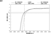
- FIG. 3 shows the attenuation frequency characteristics of the filter devices of the first embodiment and the comparative example of the present invention when the temperature is sufficiently increased, and the filter device of the first embodiment when the temperature is not increased. It is a figure which shows the attenuation amount frequency characteristic in a state.
- FIG. 4 is an enlarged view of FIG. 3, showing the vicinity of the frequency at which power is applied to the filter device.
- FIG. 5 is a schematic cross-sectional view showing part of a filter device according to a first modification of the first embodiment of the invention.
- FIG. 6 is a schematic cross-sectional view showing part of a filter device according to a second modification of the first embodiment of the invention.
- FIG. 7 is a schematic cross-sectional view showing part of a filter device according to a third modification of the first embodiment of the invention.
- FIG. 8 is a schematic cross-sectional view showing part of a filter device according to a fourth modification of the first embodiment of the invention.
- FIG. 9 is a schematic diagram of a filter device according to a second embodiment of the present invention.
- FIG. 1 is a schematic circuit diagram of the filter device according to the first embodiment of the present invention.
- the filter device 1 of this embodiment is a ladder filter.
- the filter device 1 has a first signal terminal 3A, a second signal terminal 3B, a plurality of series arm resonators, and a plurality of parallel arm resonators.
- the plurality of series arm resonators of the filter device 1 are a series arm resonator S1, a series arm resonator S2, a series arm resonator S3, a series arm resonator S4, and a series arm resonator S5.
- the plurality of parallel arm resonators are a parallel arm resonator P1, a parallel arm resonator P2, a parallel arm resonator P3 and a parallel arm resonator P4.
- all series arm resonators and all parallel arm resonators are elastic wave resonators.
- the first signal terminal 3A is an input terminal.
- the second signal terminal 3B is an antenna terminal. An antenna terminal is connected to the antenna.
- the first signal terminal 3A and the second signal terminal 3B may be configured as wiring, or may be configured as electrode pads.
- a series arm resonator S1, a series arm resonator S2, a series arm resonator S3, a series arm resonator S4, and a series arm resonator S5 are connected in series between the first signal terminal 3A and the second signal terminal 3B. It is connected.
- a parallel arm resonator P1 is connected between the connection point between the series arm resonators S1 and S2 and the ground potential.
- a parallel arm resonator P2 is connected between the connection point between the series arm resonators S2 and S3 and the ground potential.
- a parallel arm resonator P3 is connected between the connection point between the series arm resonators S3 and S4 and the ground potential.
- a parallel arm resonator P4 is connected between the connection point between the series arm resonators S4 and S5 and the ground potential.
- the circuit configuration of the filter device 1 is not limited to the above. At least one series arm resonator and at least one parallel arm resonator should be provided. However, it is preferable that a plurality of series arm resonators and a plurality of parallel arm resonators are provided. In this case, it is easy to improve the filter characteristics.
- the filter device 1 is a Band 7 transmission filter. More specifically, the pass band of the filter device 1 is 2500-2570 MHz. However, the pass band of the filter device 1 is not limited to the above. Furthermore, the filter device 1 may be a receive filter.
- the filter device 1 has multiple first wirings 6 and multiple second wirings 7 .
- a plurality of first wirings 6 respectively connect the series arm resonators and the parallel arm resonators. Furthermore, the first wiring 6 connects two series arm resonators. The first wiring 6 may connect the first signal terminal 3A or the second signal terminal 3B and the series arm resonator. The first wiring 6 should just connect the series arm resonator and the parallel arm resonator.
- each of the plurality of second wirings 7 connects the parallel arm resonator and the ground potential.
- the plurality of first wirings 6 are made of Al.
- the plurality of second wirings 7 are made of Mo.
- the materials of the plurality of first wirings 6 and the plurality of second wirings 7 are not limited to the above.
- the phrase "a certain member is made of a certain material" includes the case where a minute amount of impurity is contained to such an extent that the electrical characteristics of the filter device are not degraded.
- a specific configuration of the acoustic wave resonator in the first embodiment is shown below.
- FIG. 2 is a plan view showing the electrode configuration of the parallel arm resonator in the first embodiment. Note that the wiring connected to the parallel arm resonator P1 is omitted in FIG.
- the parallel arm resonator P1 has a piezoelectric substrate 2.
- the piezoelectric substrate 2 is a substrate consisting of only a piezoelectric layer.
- the piezoelectric layer is made of lithium tantalate.
- the material of the piezoelectric layer is not limited to the above, and lithium niobate, for example, can also be used.
- the piezoelectric substrate 2 may be a laminated substrate including piezoelectric layers.
- An IDT (Interdigital Transducer) electrode 4 as a functional electrode is provided on the piezoelectric substrate 2 .
- An AC voltage to the IDT electrodes 4 By applying an AC voltage to the IDT electrodes 4, elastic waves are excited.
- a pair of reflectors 5A and 5B are provided on both sides of the IDT electrode 4 on the piezoelectric substrate 2 in the elastic wave propagation direction.
- Each of the reflectors 5A and 5B has a plurality of electrode fingers. Both ends of a plurality of electrode fingers are short-circuited in each of the reflectors 5A and 5B.
- the IDT electrode 4 has a first busbar 8a and a second busbar 8b, and a plurality of first electrode fingers 9a and a plurality of second electrode fingers 9b.
- the first busbar 8a and the second busbar 8b face each other.
- One end of each of the plurality of first electrode fingers 9a is connected to the first bus bar 8a.
- One end of each of the plurality of second electrode fingers 9b is connected to the second bus bar 8b.
- the plurality of first electrode fingers 9a and the plurality of second electrode fingers 9b are interdigitated with each other.
- the overlapping region is the region where the adjacent first electrode fingers 9a and second electrode fingers 9b overlap each other. An acoustic wave is excited in the intersection region.
- the first electrode finger 9a and the second electrode finger 9b may be simply referred to as electrode fingers.
- the electrode finger extension direction In the following description, the first electrode finger 9a and the second electrode finger 9b may be simply referred to as electrode fingers.
- the electrode finger extension direction and the elastic wave propagation direction are orthogonal to each other.
- All acoustic wave resonators of the filter device 1 share the piezoelectric substrate 2 .
- Each acoustic wave resonator other than the parallel arm resonator P1 also has an IDT electrode and a reflector similarly to the parallel arm resonator P1.
- both the series arm resonators and the parallel arm resonators are surface acoustic wave resonators.
- the piezoelectric substrate 2 is made of lithium tantalate. Therefore, the temperature coefficient of frequency (TCF) of each surface acoustic wave resonator in the filter device 1 is a negative value.
- the plurality of first wirings 6 and the plurality of second wirings 7 shown in FIG. 1 are provided on the piezoelectric substrate 2 . Furthermore, at least one ground terminal is provided on the piezoelectric substrate 2 . Each second wiring 7 is connected to a ground terminal. The ground terminal is connected to ground potential.
- a feature of this embodiment is that the heat dissipation of all the second wirings 7 is lower than the heat dissipation of all the first wirings 6 .
- all the first wirings 6 are made of Al.
- All second wirings 7 are made of Mo.
- Al has a thermal conductivity of 236 W/m/K and Mo has a thermal conductivity of 147 W/m/K.
- the heat dissipation property of the second wiring 7 is lower than the heat dissipation property of the first wiring 6 .
- the heat dissipation of at least one second wiring 7 should be lower than the heat dissipation of all the first wirings 6 .
- the power durability can be improved without deteriorating the transmission characteristics. This will be explained below by comparing the present embodiment and a comparative example.
- the comparative example differs from the first embodiment in that both the first wiring and the second wiring are made of Al.
- the heat dissipation properties of the first wiring and the second wiring are the same.
- the attenuation frequency characteristics were compared between the first embodiment and the comparative example.
- FIG. 3 below shows attenuation frequency characteristics in a state where a sufficient amount of time has passed and the temperature has risen sufficiently after power is applied to the filter devices of the first embodiment and the comparative example.
- FIG. 3 also shows attenuation frequency characteristics in a state where the temperature does not rise immediately after power is applied to the filter device of the first embodiment.
- the attenuation frequency characteristics in a state where the temperature does not rise immediately after power is applied to the filter device are almost the same.
- Design parameters in the filter devices of the first embodiment and the comparative example are as shown in Table 1 below.
- the reference numerals indicating elastic wave resonators in Table 1 match the reference numerals indicating series arm resonators and parallel arm resonators in this specification.
- the dimension along the extending direction of the electrode fingers of the intersecting region is defined as the intersecting width.
- the wavelength of the IDT electrode is defined by the electrode finger pitch of the IDT electrode.
- the wavelength of the reflector is the wavelength defined by the electrode finger pitch of the reflector.
- the electrode finger pitch is the center-to-center distance between adjacent electrode fingers. The distance between the tip of the first electrode finger and the second bus bar or the distance between the tip of the second electrode finger and the first bus bar is defined as the inter-electrode gap length.
- FIG. 3 shows the attenuation frequency characteristics of the filter devices of the first embodiment and the comparative example when the temperature is sufficiently increased, and the attenuation of the filter device of the first embodiment when the temperature is not increased.
- FIG. 10 is a diagram showing a quantity-frequency characteristic
- FIG. 4 is an enlarged view of FIG. 3, showing the vicinity of the frequency at which power is applied to the filter device.
- the frequency for applying power to the filter device 1 may be referred to as power application frequency.
- the power application frequency is indicated by a chain double-dashed line.
- the attenuation frequency characteristic shifts to the low frequency side as a whole from the state in which the temperature does not rise to the state in which the temperature rises.
- the attenuation frequency characteristics are almost the same when the temperature does not rise. Therefore, even in the comparative example, it can be seen that the attenuation frequency characteristic is shifted to the low-frequency side as a whole as the temperature rises.
- the magnitude of the insertion loss in the comparative example is 3 dB.
- the magnitude of the insertion loss at the power application frequency is as small as 2.7 dB.
- the lower the insertion loss at the power application frequency the lower the amount of heat generated at the functional electrode. Therefore, in the first embodiment, the IDT electrode 4 as a functional electrode is less likely to be damaged, and power resistance can be improved. This is because, as shown in FIG. 4, in the first embodiment, the amount of frequency shift due to temperature rise is large on the low-pass side of the passband. Specifically, on the low-pass side of the passband, the amount of frequency shift due to temperature rise is 2.2 MHz larger in the first embodiment than in the comparative example.
- each parallel arm resonator propagates to each second wiring 7 . Then, the heat is radiated from each second wiring 7 to the outside. Alternatively, the heat is radiated to the outside through the second wirings 7, ground terminals, wirings to which the ground terminals are connected, and the like.
- the heat dissipation of each second wiring 7 in the first embodiment is low. Therefore, the heat dissipation of each parallel arm resonator is also low.
- the amount of change in resonance frequency in each parallel arm resonator increases as the temperature rises. Along with this, in the attenuation amount frequency characteristic of the filter device 1 as well, the amount of frequency shift on the low-pass side of the passband increases.
- the insertion loss is reduced at the power application frequency, and the power durability can be improved.
- the heat dissipation of the second wiring 7 is lowered, instead of adjusting the elastic wave resonator itself, which deteriorates the transmission characteristics, for example. Therefore, it is possible to improve the power durability without deteriorating the transmission characteristics.
- the heat dissipation of all the second wirings 7 is lower than the heat dissipation of all the first wirings 6 . Thereby, power durability can be improved more reliably.
- the materials of the first wiring 6 and the second wiring 7 are different. More specifically, the thermal conductivity of the material of the second wiring 7 is lower than the thermal conductivity of the material of the first wiring 6 . As a result, the heat dissipation of the second wiring 7 is lower than that of the first wiring 6 .
- the heat dissipation property of the second wiring 7 may be lower than the heat dissipation property of the first wiring 6 by a configuration other than the above. An example of this is shown below by a first modification and a second modification of the first embodiment. A first variant and a second variant are illustrated by the following schematic sectional views.
- each acoustic wave resonator is shown by a schematic diagram of a rectangle with two diagonal lines added.
- the series arm resonator S1 the parallel arm resonator P1
- the first wiring 6 and the second wiring 7 are schematically shown side by side.
- the arrangement of each elastic wave resonator and each wiring is not particularly limited.
- the piezoelectric substrate 2 is covered with a plurality of series arm resonators, a plurality of parallel arm resonators, a plurality of first wirings 6 and a plurality of second wirings 7.
- a dielectric film is provided. More specifically, the dielectric films include a first dielectric film 18A, a second dielectric film 18B, a third dielectric film 18C and a fourth dielectric film 18D.
- a first dielectric film 18A covers each first wiring 6 .
- a second dielectric film 18B covers each second wiring 7 .
- a third dielectric film 18C covers each elastic wave resonator.
- a fourth dielectric film 18 ⁇ /b>D covers the ground terminal 19 .
- the first dielectric film 18A, the second dielectric film 18B, the third dielectric film 18C, and the fourth dielectric film 18D are integrally provided.
- the first dielectric film 18A, the second dielectric film 18B, the third dielectric film 18C and the fourth dielectric film 18D may be provided separately.
- FIG. 5 the boundary between the first dielectric film 18A, the second dielectric film 18B, the third dielectric film 18C and the fourth dielectric film 18D, the second wiring 7 and the ground terminal 19 boundaries are indicated by dashed lines. The same applies to other schematic cross-sectional views.
- the thickness of the second dielectric film 18B is thicker than the thickness of the first dielectric film 18A.
- the heat dissipation property of the second wiring 7 is lower than the heat dissipation property of the first wiring 6 .
- the thicknesses of the third dielectric film 18C and the fourth dielectric film 18D are not particularly limited.
- the thickness of the third dielectric film 18C is the same as the thickness of the first dielectric film 18A.
- the thickness of the fourth dielectric film 18D is the same as the thickness of the second dielectric film 18B.
- the first dielectric film 18A, the second dielectric film 18B, the third dielectric film 18C and the fourth dielectric film 18D are silicon oxide films.
- the materials of the first dielectric film 18A, the second dielectric film 18B, the third dielectric film 18C and the fourth dielectric film 18D are not limited to silicon oxide, and may be silicon nitride or oxynitride. Silicon or the like can also be used.
- the first wiring 6 and the second wiring 7 may be made of the same material.
- the arithmetic mean roughness of the second wiring 7 is smaller than the arithmetic mean roughness of the first wiring 6.
- the heat dissipation of the second wiring 7 is lower than that of the first wiring 6 .
- the first wiring 6 and the second wiring 7 may be made of the same material.
- the arithmetic mean roughness in this specification conforms to the arithmetic mean roughness Ra in JIS B 0601:2001.
- the piezoelectric substrate 12A has a first portion 12c and a second portion 12d.
- the first portion 12c is a portion of the piezoelectric substrate 12A where the first wiring 6 is provided.
- the second portion 12d is a portion of the piezoelectric substrate 12A where the second wiring 7 is provided.
- the arithmetic mean roughness of the second portion 12d is smaller than the arithmetic mean roughness of the first portion 12c.
- the arithmetic mean roughness of the second wiring 7 is reduced by providing the second wiring 7 in a portion of the piezoelectric substrate 12A where the arithmetic mean roughness is small. In this case, the arithmetic mean roughness of the second wirings 7 can be easily made smaller than the arithmetic mean roughness of the first wirings 6 .
- the first wiring 6 and the second wiring 7 may be subjected to surface treatment such as blasting, and the surface treatment conditions may be different between the first wiring 6 and the second wiring 7. .
- the arithmetic mean roughness of the second wiring 7 may be smaller than the arithmetic mean roughness of the first wiring 6 .
- the arithmetic mean roughness in the piezoelectric substrate 12A may be the same in the first portion 12c and the second portion 12d.
- a first dielectric film 18A, a second dielectric film 18B, a third dielectric film 18C and a fourth dielectric film 18D are provided.
- the thickness of each dielectric film is the same.
- the second wiring 7 is made of an amorphous solid.
- amorphous solids the arrangement of atoms is random. Therefore, lattice vibration is difficult to propagate, and the mean free path of phonons is short.
- the thermal conductivity of amorphous solids is significantly lower than that of crystalline solids.
- the second wiring 7 of this modified example is made of an amorphous solid, the heat dissipation of the second wiring 7 can be further reduced. As a result, it is possible to further increase the amount of change in the resonance frequency of the parallel arm resonator that accompanies temperature rise. Therefore, the insertion loss can be more reliably reduced at the power application frequency, and the power durability can be more reliably increased.
- the first wiring 6 may be made of a crystalline solid.
- the first wiring 6 may be made of, for example, a single crystal or a polycrystal. More specifically, the first wiring 6 may be made of, for example, an epitaxially grown oriented film.
- an epitaxially grown oriented film refers to a polycrystalline film having a twin crystal structure.
- the piezoelectric substrate 2 in the first embodiment consists of only the piezoelectric layer.
- the piezoelectric substrate 2 may be a laminated substrate including piezoelectric layers.
- the piezoelectric substrate 12B includes a supporting substrate 13, a high acoustic velocity film 14 as a high acoustic velocity material layer, a low acoustic velocity film 15, and a piezoelectric and a body layer 16 .
- a high acoustic velocity film 14 is provided on the support substrate 13 .
- a low acoustic velocity film 15 is provided on the high acoustic velocity film 14 .
- a piezoelectric layer 16 is provided on the low-frequency film 15 .
- the heat dissipation of the second wiring 7 is lower than that of the first wiring 6, as in the first embodiment. As a result, the power durability can be improved without deteriorating the transmission characteristics.
- the low sound velocity film 15 is a relatively low sound velocity film. More specifically, the acoustic velocity of the bulk wave propagating through the low velocity film 15 is lower than the acoustic velocity of the bulk wave propagating through the piezoelectric layer 16 .
- the material of the low sound velocity film 15 for example, glass, silicon oxide, silicon oxynitride, lithium oxide, tantalum pentoxide, or a material mainly composed of a compound obtained by adding fluorine, carbon, or boron to silicon oxide may be used. can be done.
- the main component means a component that accounts for more than 50 wt %.
- the material of the main component may exist in a single crystal, polycrystal, or amorphous state, or in a state in which these are mixed.
- the high acoustic velocity material layer is a relatively high acoustic velocity layer.
- the high acoustic velocity material layer is the high acoustic velocity film 14 .
- the acoustic velocity of bulk waves propagating through the high acoustic velocity material layer is higher than the acoustic velocity of elastic waves propagating through the piezoelectric layer 16 .
- Materials for the high-sonic material layer include, for example, aluminum nitride, lithium tantalate, lithium niobate, piezoelectrics such as crystal, alumina, sapphire, magnesia, silicon nitride, silicon carbide, zirconia, cordierite, mullite, steatite, Ceramics such as forsterite, spinel, sialon, etc., aluminum oxide, silicon oxynitride, DLC (diamond-like carbon), dielectrics such as diamond, semiconductors such as silicon, or materials containing the above materials as main components can be used.
- the above spinel includes an aluminum compound containing one or more elements selected from Mg, Fe, Zn, Mn, etc. and oxygen. Examples of the spinels include MgAl2O4 , FeAl2O4 , ZnAl2O4 , and MnAl2O4 .
- Materials for the support substrate 13 include, for example, aluminum oxide, lithium tantalate, lithium niobate, piezoelectric materials such as crystal, alumina, sapphire, magnesia, silicon nitride, aluminum nitride, silicon carbide, zirconia, cordierite, mullite, and steer.
- Various ceramics such as tight and forsterite, dielectrics such as diamond and glass, semiconductors such as silicon and gallium nitride, and resins can be used.
- a high acoustic velocity film 14 as a high acoustic velocity material layer, a low acoustic velocity film 15 and a piezoelectric layer 16 are laminated in this order on the piezoelectric substrate 12B. Thereby, the elastic wave energy can be effectively confined to the piezoelectric layer 16 side.
- the laminated structure of the piezoelectric substrate is not limited to the above.
- the piezoelectric substrate may be a laminated substrate of a supporting substrate, a high acoustic velocity film and a piezoelectric layer.
- the high acoustic velocity material layer may be a high acoustic velocity support substrate.
- the piezoelectric substrate may be a laminated substrate of a high acoustic velocity supporting substrate, a low acoustic velocity film and a piezoelectric layer, or may be a laminated substrate of a high acoustic velocity supporting substrate and a piezoelectric layer.
- the energy of elastic waves can be effectively confined in the piezoelectric layer.
- FIG. 9 is a schematic diagram of a filter device according to the second embodiment.
- the filter device 20 of this embodiment is a composite filter device. More specifically, filter device 20 is a multiplexer.
- filter devices other than composite filter devices such as band-pass filters, may be referred to as filters.
- the filter device 20 has a common connection terminal 22, a first filter 21A, a second filter 21B, a third filter 21C, and at least one other filter.
- a plurality of filters are commonly connected to a common connection terminal 22 .
- the common connection terminal 22 may be configured as wiring, or may be configured as an electrode pad. Note that the number of filters in the filter device 20 is not particularly limited. If filter device 20 is a multiplexer, filter device 20 need only have three or more filters.
- the first filter 21A, the second filter 21B and the third filter 21C are band-pass filters.
- the first filter 21A is a transmission filter having a configuration similar to that of the first embodiment.
- the first filter 21A may be any filter according to the present invention.
- the filter device 20 need only have at least one filter according to the invention.
- the filter device 20 has a first filter 21A configured similarly to the first embodiment. Therefore, it is possible to improve the power durability without deteriorating the transmission characteristics.
- the filter device 20 may be a duplexer or the like having two filters. Also in this case, the filter device 20 only needs to have at least one filter according to the invention.
- Reference Signs List 1 Filter device 2 Piezoelectric substrates 3A, 3B First and second signal terminals 4 IDT electrodes 5A and 5B Reflectors 6 and 7 First and second wirings 8a and 8b First and second 2 bus bars 9a, 9b... first and second electrode fingers 12A, 12B... piezoelectric substrates 12c, 12d... first and second portions 13... support substrate 14... high acoustic velocity film 15... low acoustic velocity film 16... piezoelectric Body layers 18A to 18D First to fourth dielectric films 19 Ground terminal 20 Filter devices 21A to 21C First to third filters 22 Common connection terminals P1 to P4 Parallel arm resonators S1 to S5 ... series arm resonator
Landscapes
- Physics & Mathematics (AREA)
- Acoustics & Sound (AREA)
- Surface Acoustic Wave Elements And Circuit Networks Thereof (AREA)
Abstract
L'invention concerne un dispositif de filtre qui permet d'augmenter la durabilité de puissance sans provoquer de dégradation des caractéristiques de transmission. Un dispositif de filtre 1 selon la présente invention comprend : un substrat piézoélectrique ; des résonateurs à bras série S1 à S5 configurés sur le substrat piézoélectrique ; des résonateurs à bras parallèles P1 à P4 configurés sur le substrat piézoélectrique ; des premières lignes de câblage 6 disposées sur le substrat piézoélectrique et reliant les résonateurs à bras série et les résonateurs à bras parallèles ; et des deuxièmes lignes de câblage 7 disposées sur le substrat piézoélectrique et reliant les résonateurs à bras parallèles au potentiel de masse. La dissipation thermique d'au moins une deuxième ligne de câblage 7 est inférieure à celle de toutes les premières lignes de câblage 6.
Applications Claiming Priority (2)
| Application Number | Priority Date | Filing Date | Title |
|---|---|---|---|
| JP2021170416 | 2021-10-18 | ||
| JP2021-170416 | 2021-10-18 |
Publications (1)
| Publication Number | Publication Date |
|---|---|
| WO2023068128A1 true WO2023068128A1 (fr) | 2023-04-27 |
Family
ID=86058233
Family Applications (1)
| Application Number | Title | Priority Date | Filing Date |
|---|---|---|---|
| PCT/JP2022/038012 Ceased WO2023068128A1 (fr) | 2021-10-18 | 2022-10-12 | Dispositif de filtre |
Country Status (1)
| Country | Link |
|---|---|
| WO (1) | WO2023068128A1 (fr) |
Citations (5)
| Publication number | Priority date | Publication date | Assignee | Title |
|---|---|---|---|---|
| JP2004282707A (ja) * | 2003-02-24 | 2004-10-07 | Murata Mfg Co Ltd | 弾性表面波フィルタ、通信機 |
| JP2007068231A (ja) * | 2006-11-30 | 2007-03-15 | Oki Electric Ind Co Ltd | 弾性表面波フィルタ及び弾性表面波フィルタパッケージ |
| JP2007074459A (ja) * | 2005-09-08 | 2007-03-22 | Hitachi Media Electoronics Co Ltd | 共振器型フィルタ |
| JP2020170983A (ja) * | 2019-04-05 | 2020-10-15 | 三安ジャパンテクノロジー株式会社 | 表面弾性波デバイス及びその製造方法 |
| JP2020198552A (ja) * | 2019-06-03 | 2020-12-10 | 太陽誘電株式会社 | 弾性波デバイス、フィルタ、及びマルチプレクサ |
-
2022
- 2022-10-12 WO PCT/JP2022/038012 patent/WO2023068128A1/fr not_active Ceased
Patent Citations (5)
| Publication number | Priority date | Publication date | Assignee | Title |
|---|---|---|---|---|
| JP2004282707A (ja) * | 2003-02-24 | 2004-10-07 | Murata Mfg Co Ltd | 弾性表面波フィルタ、通信機 |
| JP2007074459A (ja) * | 2005-09-08 | 2007-03-22 | Hitachi Media Electoronics Co Ltd | 共振器型フィルタ |
| JP2007068231A (ja) * | 2006-11-30 | 2007-03-15 | Oki Electric Ind Co Ltd | 弾性表面波フィルタ及び弾性表面波フィルタパッケージ |
| JP2020170983A (ja) * | 2019-04-05 | 2020-10-15 | 三安ジャパンテクノロジー株式会社 | 表面弾性波デバイス及びその製造方法 |
| JP2020198552A (ja) * | 2019-06-03 | 2020-12-10 | 太陽誘電株式会社 | 弾性波デバイス、フィルタ、及びマルチプレクサ |
Similar Documents
| Publication | Publication Date | Title |
|---|---|---|
| US11444601B2 (en) | Acoustic wave device | |
| US20220224311A1 (en) | Acoustic wave device | |
| CN109845105B (zh) | 弹性波滤波器装置 | |
| US12470197B2 (en) | Acoustic wave device | |
| US12355425B2 (en) | Acoustic wave device | |
| US11996828B2 (en) | Filter device | |
| US12289096B2 (en) | Acoustic wave filter device | |
| US20240154595A1 (en) | Acoustic wave device | |
| WO2022102621A1 (fr) | Dispositif à ondes élastiques | |
| US20240380377A1 (en) | Acoustic wave device | |
| WO2022158363A1 (fr) | Dispositif à ondes élastiques | |
| US20240243728A1 (en) | Filter device | |
| WO2023068128A1 (fr) | Dispositif de filtre | |
| WO2023068129A1 (fr) | Dispositif de filtre | |
| US20220263493A1 (en) | Acoustic wave device | |
| CN118511434A (zh) | 弹性波装置 | |
| WO2023140354A1 (fr) | Dispositif à ondes élastiques et dispositif de filtre | |
| CN118511432A (zh) | 弹性波装置 | |
| WO2022224740A1 (fr) | Filtre de type échelle | |
| WO2022102620A1 (fr) | Dispositif de filtrage | |
| US20250175139A1 (en) | Acoustic wave device | |
| US12445106B2 (en) | Acoustic wave device | |
| US20260113015A1 (en) | Acoustic wave device and filter device | |
| US20240275354A1 (en) | Acoustic wave device | |
| WO2024080205A1 (fr) | Dispositif de filtre |
Legal Events
| Date | Code | Title | Description |
|---|---|---|---|
| 121 | Ep: the epo has been informed by wipo that ep was designated in this application |
Ref document number: 22883432 Country of ref document: EP Kind code of ref document: A1 |
|
| NENP | Non-entry into the national phase |
Ref country code: DE |
|
| 122 | Ep: pct application non-entry in european phase |
Ref document number: 22883432 Country of ref document: EP Kind code of ref document: A1 |
|
| NENP | Non-entry into the national phase |
Ref country code: JP |