WO2023084981A1 - 電子機器 - Google Patents
電子機器 Download PDFInfo
- Publication number
- WO2023084981A1 WO2023084981A1 PCT/JP2022/037987 JP2022037987W WO2023084981A1 WO 2023084981 A1 WO2023084981 A1 WO 2023084981A1 JP 2022037987 W JP2022037987 W JP 2022037987W WO 2023084981 A1 WO2023084981 A1 WO 2023084981A1
- Authority
- WO
- WIPO (PCT)
- Prior art keywords
- antenna
- electronic device
- antenna module
- housing
- predetermined
- Prior art date
- Legal status (The legal status is an assumption and is not a legal conclusion. Google has not performed a legal analysis and makes no representation as to the accuracy of the status listed.)
- Ceased
Links
Images


Classifications
-
- H—ELECTRICITY
- H01—ELECTRIC ELEMENTS
- H01Q—ANTENNAS, i.e. RADIO AERIALS
- H01Q1/00—Details of, or arrangements associated with, antennas
- H01Q1/12—Supports; Mounting means
- H01Q1/22—Supports; Mounting means by structural association with other equipment or articles
- H01Q1/24—Supports; Mounting means by structural association with other equipment or articles with receiving set
-
- H—ELECTRICITY
- H01—ELECTRIC ELEMENTS
- H01Q—ANTENNAS, i.e. RADIO AERIALS
- H01Q1/00—Details of, or arrangements associated with, antennas
- H01Q1/42—Housings not intimately mechanically associated with radiating elements, e.g. radome
-
- H—ELECTRICITY
- H01—ELECTRIC ELEMENTS
- H01Q—ANTENNAS, i.e. RADIO AERIALS
- H01Q1/00—Details of, or arrangements associated with, antennas
- H01Q1/12—Supports; Mounting means
- H01Q1/22—Supports; Mounting means by structural association with other equipment or articles
- H01Q1/2258—Supports; Mounting means by structural association with other equipment or articles used with computer equipment
- H01Q1/2266—Supports; Mounting means by structural association with other equipment or articles used with computer equipment disposed inside the computer
-
- H—ELECTRICITY
- H01—ELECTRIC ELEMENTS
- H01Q—ANTENNAS, i.e. RADIO AERIALS
- H01Q19/00—Combinations of primary active antenna elements and units with secondary devices, e.g. with quasi-optical devices, for giving the antenna a desired directional characteristic
- H01Q19/10—Combinations of primary active antenna elements and units with secondary devices, e.g. with quasi-optical devices, for giving the antenna a desired directional characteristic using reflecting surfaces
-
- H—ELECTRICITY
- H01—ELECTRIC ELEMENTS
- H01Q—ANTENNAS, i.e. RADIO AERIALS
- H01Q21/00—Antenna arrays or systems
- H01Q21/06—Arrays of individually energised antenna units similarly polarised and spaced apart
- H01Q21/08—Arrays of individually energised antenna units similarly polarised and spaced apart the units being spaced along or adjacent to a rectilinear path
Definitions
- This disclosure relates to electronic equipment.
- Patent Document 1 discloses an antenna module housing structure for housing an antenna module configured by forming an antenna on a substrate in a housing.
- the housing is made of resin and has the shape of a hollow box, and rectangular side plates are formed on each side of the hexahedron.
- An RF antenna module is housed in a side plate located in front of the housing by means of an antenna module housing structure.
- the RF antenna module radiates millimeter-wave radio waves forward in front of the side plate exposed to the outside of the housing from the patch antenna that constitutes the front radiation antenna.
- tilting the antenna module with respect to the side plate of the housing is conceivable as a method of changing the direction of radiation of millimeter-wave radio waves. If the antenna module is tilted with respect to the side plate, the distance between the antenna module and the side plate will not be uniform. This can contribute to degraded antenna performance of the antenna module.
- the present disclosure provides an electronic device in which the main radiation direction of the antenna module can be tilted with respect to the housing without tilting the antenna module with respect to the housing.
- An electronic device includes an antenna module for communicating at a predetermined communication frequency, a housing having a predetermined surface and a recess provided on the predetermined surface.
- the antenna module is accommodated in the recess such that the plane direction of the antenna surface of the antenna module matches the plane direction of the predetermined plane.
- the predetermined surface includes a first area and a second area that are opposite to each other with respect to the recess in the width direction of the antenna surface.
- the housing has a conductive protrusion in the first region. The tip of the protrusion protrudes in the plane direction of the antenna surface from the antenna surface. The second region does not project beyond the antenna surface in the plane direction of the antenna surface.
- the main radiation direction of the antenna module can be tilted with respect to the housing without tilting the antenna module with respect to the housing.
- FIG. 1 is a block diagram of a configuration example of a circuit of an electronic device according to an embodiment
- FIG. Schematic perspective view of the electronic device of FIG. The partial perspective view which notched a part of site
- FIG. 1 is a block diagram of a circuit configuration example of an electronic device 1 according to this embodiment.
- the electronic device 1 in FIG. 1 is a laptop computer.
- the electronic device 1 includes an antenna module 2 , a communication circuit 31 , an input/output device 32 , a storage device 33 and an arithmetic circuit 34 .
- the antenna module 2 is used for communication on a predetermined communication frequency. Although details will be described later, the antenna module 2 includes a plurality of antenna elements 21 on the antenna surface 20 .
- the antenna module 2 is used for transmitting and receiving radio waves of a predetermined communication frequency.
- the predetermined communication frequency is included in a frequency band of 24.250 GHz to 52.600 GHz, for example.
- the frequency band from 24.250 GHz to 52.600 GHz is defined as the FR2 frequency band for 5GNR.
- FR2 further includes frequency bands represented by band numbers n257, n258, n260, and n261.
- n257 and n261 are in the 28 GHz band.
- n258 is in the 26 GHz band.
- n260 is in the 39 GHz band.
- the antenna module 2 is an antenna module for quasi-millimeter wave band to millimeter wave band.
- the antenna module 2 is used for wireless communication between the electronic device 1 and an external device.
- the communication circuit 31 is connected to the antenna module 2.
- the communication circuit 31 is communicably connected to an external device or system via the antenna module 2 .
- the communication circuit 31 has one or more communication interfaces.
- the communication circuit 31 complies with a predetermined communication protocol.
- the predetermined communication protocol may be selected from various well-known wireless communication standards.
- the input/output device 32 functions as an input device for inputting information from the user and as an output device for outputting information to the user. That is, the input/output device 32 is used for inputting information to the electronic device 1 and outputting information from the electronic device 1 .
- Input/output device 32 comprises one or more human-machine interfaces. Examples of human-machine interfaces include keyboards, pointing devices (mouse, trackball, etc.), input devices such as touch pads, output devices such as displays and speakers, and input/output devices such as touch panels. In FIG. 2, input/output device 32 comprises keyboard 321 and display 322 .
- Input/output device 32 may comprise one or more connectors. Examples of the one or more connectors include earphone jacks, USB connectors, LAN connectors, HDMI connectors, DVI connectors, D-sub connectors.
- the storage device 33 is used to store information used by the arithmetic circuit 34 and information generated by the arithmetic circuit 34 .
- the storage device 13 includes one or more storages (non-temporary storage media).
- the storage can be, for example, hard disk drives, optical drives, and solid state drives (SSDs).
- the arithmetic circuit 34 is a circuit that controls the operation of the electronic device 1 .
- the arithmetic circuit 34 is connected to the communication circuit 31 and the input/output device 32 and can access the storage device 33 .
- Arithmetic circuit 34 may be realized by, for example, a computer system including one or more processors (microprocessors) and one or more memories.
- processors microprocessors
- One or more processors execute programs (stored in one or more memories or storage devices 33) to implement predetermined functions.
- the program is pre-recorded in the storage device 33 here, it may be provided through an electric communication line such as the Internet or recorded in a non-temporary recording medium such as a memory card.
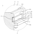
- FIG. 2 is a schematic perspective view of the electronic device 1 of FIG.
- the electronic device 1 includes a housing 4 that houses an antenna module 2 , a communication circuit 31 , an input/output device 32 , a storage device 33 and an arithmetic circuit 34 .
- the housing 4 in FIG. 2 includes a first housing 5 and a second housing 6.
- the first housing 5 corresponds to the base or bottom of the laptop computer.
- the first housing 5 has a flat rectangular parallelepiped shape.
- the first housing 5 accommodates the antenna module 2 , the communication circuit 31 , the input/output device 32 excluding the display 322 , the storage device 33 , and the arithmetic circuit 34 .
- a keyboard 321 is arranged on the upper surface of the first housing 5 .
- a second housing 6 corresponds to the cover of a laptop computer.
- the second housing 6 has a flat rectangular parallelepiped shape.
- the second housing 6 accommodates the display 322 .
- the second housing 6 is attached to the first housing 5 so as to be rotatable between an open position where the display 322 is visible from the user and a closed position where the display 322 is invisible from the user. Since the second housing 6 is rotatable with respect to the first housing 5 , the length direction, width direction and thickness direction of the housing 4 are determined based on the first housing 5 . That is, the length direction, width direction, and thickness direction of the first housing 5 correspond to the length direction, width direction, and thickness direction of the housing 4, respectively.
- the first housing 5 has conductivity.
- the first housing 5 is made of a conductive material such as a metal material.
- a metal material is, for example, magnesium.
- the antenna module 2 is in the vicinity of the predetermined plane 51 of the first housing 5 of the housing 4 .
- the predetermined surface 51 is a longitudinal side surface of the first housing 5 in the present embodiment.
- the length direction of the predetermined surface 51 coincides with the width direction of the first housing 5 .
- the width of the predetermined surface 51 matches the thickness direction of the first housing 5 .
- the predetermined surface 51 is the right side located on the right side of the user when the electronic device 1 is in use.
- FIG. 3 is a partial perspective view with a part of the portion indicated by P in FIG. 2 cut away. 4 is a partial side view of the portion indicated by P in FIG. 2. FIG. In addition, in FIG. 3, the antenna module 2 is illustrated in a simplified manner.
- the electronic device 1 includes a radome 7 covering the antenna module 2.
- a recess 510 in which the radome 7 is fitted is formed in the predetermined surface 51 .
- a bottom surface 510 a of the recess 510 is formed with a recess 52 capable of accommodating the antenna module 2 . That is, a concave portion 52 is provided on the predetermined surface 51 of the first housing 5 .
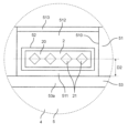
- FIG. 5 is a diagram in which the radome 7 is omitted from FIG.
- FIG. 6 is a diagram in which the radome 7 is omitted from FIG.
- the antenna module 2 is illustrated in a simplified manner.
- the antenna module 2 has a rectangular plate shape.
- the antenna module 2 has a thickness direction (horizontal direction in FIG. 5), a length direction (horizontal direction in FIG. 6), and a width direction (vertical direction in FIG. 6).
- the antenna module 2 has an antenna surface 20 on one surface in the thickness direction.
- the antenna element 21 is, for example, an electrode formed on the antenna surface 20 and resonating at a predetermined communication frequency.
- the plurality of antenna elements 21 are arranged in a line in the length direction of the antenna surface 20 . This allows the antenna module 2 to be used as a phased array antenna.
- the length direction of the antenna plane 20 is the array direction in which the antenna elements 21 are arranged on the antenna plane 20 .
- the width direction of the antenna plane 20 is the non-array direction in which the antenna elements 21 are not arranged on the antenna plane 20 .
- the recess 52 has a substantially rectangular shape.
- the size of the concave portion 52 is larger than the size of the antenna module 2 when viewed from the thickness direction of the antenna module 2 .
- the lengthwise direction of the concave portion 52 coincides with the lengthwise direction of the predetermined surface 51 .
- the width direction of the concave portion 52 coincides with the width direction of the predetermined surface 51 , that is, the thickness direction of the housing 4 .
- the antenna module 2 is placed inside the recess 52 so that the plane direction of the antenna surface 20 of the antenna module 2 matches the plane direction of the predetermined plane 51 .
- the plane direction means a direction perpendicular to the plane. That is, the antenna module 2 is accommodated in the recess 52 so that the antenna surface 20 is parallel to the predetermined surface 51 .
- the antenna module 2 is within the recess 52 such that the antenna surface 20 is outside the recess 52 . That is, the antenna surface 20 protrudes outward from the concave portion 52 .
- the center position of the antenna surface 20 of the antenna module 2 in the width direction and the center position of the recess 52 in the width direction coincide with each other.
- the antenna module 2 is connected to the communication circuit 31 by an electric wire or the like using an opening that connects the inside of the recess 52 and the inside of the first housing 5 .
- the antenna module 2 a plurality of antenna elements 21 are arranged in a line in the length direction of the antenna surface 20.
- the communication circuit 31 can control the directivity of the antenna module 2 in a plane perpendicular to the width direction of the antenna surface 20 by beamforming technology.
- beam forming technology can be used in a plane orthogonal to the length direction of the antenna surface 20. Directivity control is not possible. Therefore, in the plane orthogonal to the length direction of the antenna plane 20 , the main radiation direction of the antenna module 2 coincides with the planar direction of the predetermined plane 51 in the antenna module 2 alone.
- the dotted arrow A1 indicates the main radiation direction of the antenna module 2 that coincides with the plane direction of the predetermined plane 51 .
- the electronic device 1 is a laptop computer.
- it is desirable that the antenna gain of the antenna module 2 is secured in the upper hemispherical region of 90 degrees from the zenith.
- the solid arrow A2 indicates the main radiation direction of the antenna module 2 tilted upward with respect to the plane direction of the predetermined plane 51 .
- the distance between the antenna surface 20 and the radome 7 becomes uneven, which greatly affects the antenna characteristics of the radome 7. and may contribute to deterioration of antenna characteristics.
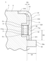
- a structure for adjusting the main radiation direction of the antenna module 2 is provided on the predetermined surface 51 .
- the predetermined surface 51 includes a first region 511 and a second region 512 that are opposite to each other with respect to the recess 52 in the width direction of the antenna surface 20.
- the first region 511 is a region on the predetermined surface 51 closer to the bottom surface of the first housing 5 (lower side in FIG. 6) than the recessed portion 52 is.
- the second region 512 is a region on the upper surface side (upper side in FIG. 6) of the first housing 5 than the concave portion 52 on the predetermined surface 51 .
- the first region 511 and the second region 512 are flat.
- the first housing 5 has a projection 53 in the first region 511. That is, the housing 4 has the protrusion 53 in the first region 511 .
- the protrusion 53 has conductivity.
- the protrusion 53 is formed of a conductive material such as a metal material.
- a metal material is, for example, magnesium.
- the projection 53 is formed integrally with the first housing 5 . As shown in FIG. 6, in this embodiment, the protrusion 53 extends over the entire length of the antenna surface 20 .
- the protrusion 53 has a tip 53a.
- the tip 53a is a flat surface.
- the first housing 5 does not have a structure like the projection 53 in the second area 512.
- the second region 512 includes the edge (the upper end in the present embodiment) of the predetermined surface 51 .
- the edge of the predetermined surface 51 has a stepped portion 513 that is recessed in a direction opposite to the planar direction of the antenna surface 20 relative to the antenna surface 20 .
- the stepped portion 513 extends over the entire length of the antenna surface 20 . As shown in FIGS. 5 and 6, both the second region 512 and the stepped portion 513 are flat, but the portion from the second region 512 to the stepped portion 513 has an R shape.
- FIG. 7 is a partial cross-sectional view of the vicinity of the antenna module 2 of the electronic device 1. As shown in FIG.
- the tip 53a of the protrusion 53 protrudes from the antenna surface 20 in the planar direction of the antenna surface 20 (rightward in FIG. 7).
- a distance D1 between the tip 53a of the protrusion 53 and the antenna surface 20 is 0.15 times or more and 0.40 times or less the wavelength corresponding to the predetermined communication frequency. More specifically, the distance D1 is the distance between the antenna surface 20 and the tip 53a in the surface direction of the antenna surface 20.
- a distance D2 between the widthwise center of the antenna surface 20 and the protrusion 53 is 0.30 times or more and 0.8 times or less the wavelength corresponding to the predetermined communication frequency. More specifically, the distance D2 is the distance between the widthwise center of the antenna surface 20 and the side surface of the protrusion 53 on the antenna module 2 side in the widthwise direction of the antenna surface 20 .
- the second region 512 does not protrude from the antenna surface 20 in the plane direction of the antenna surface 20 . Unlike the first region 511 with the protrusion 53 , the second region 512 does not protrude beyond the antenna plane 20 in the planar direction of the antenna plane 20 . That is, the second region 512 may be on the same plane as the antenna surface 20 or recessed from the antenna surface 20 . A portion of the housing 4 near the second region 512 is made easier for radio waves from the antenna module 2 to pass through. A step portion 513 is present in the second region 512 . The step portion 513 can reduce the volume of the housing 4 on the second region 512 side from the antenna module 2 . This makes it easier for radio waves from the antenna module 2 to pass through.
- the stepped portion 513 is located on the opposite side of the bottom surface 521 of the recess 52 from the predetermined surface 51 (on the left side in FIG. 7).
- a distance D3 from the antenna surface 20 to the predetermined surface 51 in the surface direction of the antenna surface 20 is, for example, 0.03 to 0.05 times the wavelength corresponding to the predetermined communication frequency. This makes it easier for radio waves from the antenna module 2 to pass through.
- the first region 511 has the conductive protrusion 53 whose tip 53a protrudes in the plane direction of the antenna plane 20 from the antenna plane 20.
- the region 512 does not protrude from the antenna surface 20 in the planar direction of the antenna surface 20 . Therefore, of the radio waves radiated from the antenna surface 20 of the antenna module 2 , part of the radio waves traveling toward the first region 511 are reflected by the projection 53 and travel toward the second region 512 . On the other hand, of the radio waves radiated from the antenna surface 20 of the antenna module 2, part of the radio waves traveling toward the second region 512 travels without being disturbed.
- the radiation pattern of the antenna module 2 decreases on the first area 511 side and increases on the second area 512 side. As a result, the main radiation direction of the antenna module 2 is tilted toward the second region 512 without tilting the antenna module 2 itself. Therefore, according to the electronic device 1 , the main radiation direction of the antenna module 2 can be tilted with respect to the housing 4 without tilting the antenna module 2 with respect to the housing 4 .
- a radome 7 is attached to the first housing 5 as shown in FIGS.
- a radome 7 protects the antenna module 2 .
- the radome 7 is made of a dielectric material such as a resin material so as to pass radio waves from the antenna module 2 or radio waves to the antenna module 2 .
- the radome 7 includes a first portion 71 , a second portion 72 and a spacer 73 .
- the first part 71 covers the antenna surface 20.
- the first portion 71 has a rectangular plate shape with a size that covers the antenna surface 20 .
- the first portion 71 includes a facing portion 71a.
- the facing portion 71a has a facing region 711a facing parallel to the antenna surface 20 .
- the facing portion 71a protrudes toward the antenna surface 20 side.
- the shape of the antenna surface 20 and the shape of the facing portion 71a are the same.
- a surface of the facing portion 71 a on the side of the antenna surface 20 is a facing region 711 a facing the antenna surface 20 in parallel.
- the opposing portion 71a is symmetrical with respect to a line passing through the center of the antenna surface 20 in the width direction.
- the thickness of the facing portion 71a is uniform. Both surfaces in the thickness direction of the opposing portion 71a are flat surfaces.
- the facing portion 71a it is possible to reduce the possibility that the radiation characteristics of the antenna module 2 are disturbed by the facing portion 71a and the radiation becomes stronger or weaker in an unintended direction. As a result, the gain in the front direction (antenna surface 20 direction) of the antenna module 2 can be improved.
- the second portion 72 extends from the first portion 71 and hits the stepped portion 513 . More specifically, the second portion 72 extends from one end (upper end in FIG. 7) of the first portion 71 .
- the second portion 72 is formed integrally with the first portion 71 .
- the second portion 72 has an R-shaped connection portion with the first portion 71 .
- the second portion 72 covers the gap between one end of the first portion 71 and the step portion 513 .
- the dimensions of the second portion 72 in the plane direction of the antenna plane 20 are set so that the first portion 71 does not contact the first region 511 and the second region 512 .
- the antenna module 2 is housed in the recess 52 so that the antenna surface 20 protrudes from the recess 52 .
- the antenna surface 20 of the antenna module 2 faces the facing area 711 a of the radome 7 .
- the distance between the facing area 711 a and the antenna surface 20 is set within a predetermined distance range that can suppress the decrease in antenna gain due to the reflection of radio waves on the radome 7 .
- the predetermined distance range is, for example, 1/50 or more and 1/30 or less of the wavelength corresponding to the predetermined communication frequency of the antenna module 2 .
- the spacer 73 is used to keep the distance between the facing area 711a and the antenna surface 20 within a predetermined distance range. As shown in FIG. 7, the spacer 73 is located between the facing area 711a and the antenna surface 20 to keep the distance between the facing area 711a and the antenna surface 20 within a predetermined distance range. In this embodiment, the spacer 73 is formed in the facing region 711a. The spacer 73 is formed continuously and integrally with the first portion 71 and is a dielectric. The height of the spacer 73 is set so that the distance between the opposing area 711a and the antenna surface 20 is within a predetermined distance range when the antenna surface 20 is in contact with the spacer 73 .
- the spacer 73 is arranged so as not to face the antenna element 21 of the antenna module 2 (in the thickness direction of the antenna module 2). Furthermore, the distance between the spacer 73 and the antenna element 21 in the plane parallel to the antenna plane 20 is set so as to reduce the influence of the provision of the spacer 73 on antenna characteristics such as antenna gain and radiation directivity. set. As an example, the distance between the spacer 73 and the antenna element 21 in the plane parallel to the antenna plane 20 is within the range of 1 ⁇ 5 or more and 1 ⁇ 8 or less of the wavelength corresponding to the predetermined communication frequency.
- the antenna module 2 is accommodated in the concave portion 52 of the predetermined surface 51 of the housing 4, and the elastic member 8 is provided between the antenna module 2 and the bottom surface 521 of the concave portion 52. is placed.
- the depth of recess 52 is smaller than the thickness of antenna module 2 and the thickness of elastic member 8 . Therefore, the antenna module 2 is accommodated in the recess 52 so that the antenna surface 20 protrudes from the recess 52 .
- the electronic device 1 includes the elastic member 8 arranged between the bottom surface 521 of the recess 52 and the antenna module 2 .
- the elastic member 8 is used to position the antenna module 2 with respect to the radome 7 in the thickness direction of the antenna module 2 .
- the elastic member 8 is arranged between the antenna module 2 and the bottom surface 521 of the recess 52 . More specifically, the elastic member 8 is arranged between the antenna module 2 and the bottom surface 521 of the recess 52 while being compressed in the thickness direction of the antenna module 2 .
- the elastic member 8 has a degree of elasticity capable of withstanding the weight of the antenna module 2 and pressing the antenna module 2 against the radome 7 .
- the elastic member 8 uniformly presses the antenna module 2 against the facing region 711 a of the radome 7 . Therefore, the antenna module 2 can be positioned at a fixed position with respect to the radome 7 even if the antenna module 2 , the housing 4 , the radome 7 , and the like are expanded or contracted due to shape errors or heat. As a result, variations in antenna performance caused by variations in the distance between the antenna module 2 and the radome 7 can be reduced.
- Materials for the elastic member 8 include a cushioning material and a heat-dissipating rubber material.
- the cushion material includes foamed polyurethane, foamed polyethylene, ethylene propylene rubber, and the like.
- the heat-dissipating rubber material includes silicone, acryl, and the like.
- the elastic member 8 is made of a heat-dissipating rubber material. Therefore, the elastic member 8 has thermal conductivity. The elastic member 8 can transfer the heat generated by the antenna module 2 to the housing 4 and improve the heat dissipation of the antenna module 2 .
- FIGS. 8 to 10 are heat maps of the antenna gain of the electronic device 1.
- FIG. 11 to 13 are heat maps of antenna gains of electronic devices of comparative examples.
- ⁇ is an angle around a rotation axis extending in the width direction of the antenna module 2 through the center of the antenna module 2 in the length direction and thickness direction.
- ⁇ is an angle around the axis of rotation that passes through the center of the antenna module 2 in the width direction and thickness direction and extends in the length direction of the antenna module 2 .
- the plane direction of the antenna plane 20 is a direction in which ⁇ is 180° and ⁇ is 90°.
- 8 and 11 are the results of simulations performed with the predetermined communication frequency set to 25.875 GHz corresponding to band number n258.
- 9 and 12 show the results of simulations performed with the predetermined communication frequency set to 27.925 GHz corresponding to band number n261.
- 10 and 13 show the results of simulations performed with the predetermined communication frequency set to 38.500 GHz corresponding to band number n260.
- the main radiation direction of the antenna module 2 can be tilted with respect to the housing 4 without tilting the antenna module 2 with respect to the housing 4 .
- the electronic device 1 of the present embodiment by changing the radiation pattern in the non-array direction, which cannot be handled by the directivity control inherent in the antenna module 2, the degree of freedom of arrangement of the antenna module 2 in a laptop computer and the It is possible to achieve both antenna performance.
- the electronic device 1 described above includes an antenna module 2 for communicating at a predetermined communication frequency, and a housing 4 having a predetermined surface 51 with a concave portion 52 capable of housing the antenna module 2 .
- the antenna module 2 is placed in the recess 52 so that the plane direction of the antenna surface 20 of the antenna module 2 matches the plane direction of the predetermined plane 51 .
- the predetermined surface 51 includes a first region 511 and a second region 512 that are opposite to each other with respect to the recess 52 in the width direction of the antenna surface 20 .
- the housing 4 has a conductive projection 53 in the first region 511 .
- a tip 53 a of the protrusion 53 protrudes in the plane direction of the antenna plane 20 from the antenna plane 20 .
- the second region 512 does not protrude from the antenna surface 20 in the planar direction of the antenna surface 20 .
- the distance D1 in the surface direction of the antenna surface 20 between the tip 53a of the protrusion 53 and the antenna surface 20 is 0.15 times or more and 0.40 times or less the wavelength corresponding to the predetermined communication frequency.
- the distance D2 along the antenna surface 20 between the center of the antenna surface 20 in the width direction and the protrusion 53 is 0.30 to 0.8 times the wavelength corresponding to the predetermined communication frequency.
- the protrusion 53 extends over the entire length of the antenna surface 20.
- the second area 512 includes the edge of the predetermined surface 51 .
- the end of the predetermined surface 51 has a stepped portion 513 that is recessed from the antenna surface 20 in the direction opposite to the plane direction of the antenna surface 20 .
- the stepped portion 513 extends over the entire length of the antenna surface 20 .
- the stepped portion 513 is on the side opposite to the predetermined surface 51 with respect to the bottom surface 521 of the recessed portion 52 .
- the electronic device 1 further includes a dielectric radome 7 .
- the radome 7 includes a first portion 71 that covers the antenna surface 20 and a second portion 72 that extends from the first portion 71 and contacts the stepped portion 513 . With this configuration, the main radiation direction of the antenna module 2 can be tilted with respect to the housing 4 without tilting the antenna module 2 with respect to the housing 4 .
- the first portion 71 includes a facing portion 71 a having a facing area 711 a facing parallel to the antenna surface 20 .
- the thickness of the facing portion 71a is uniform. This configuration can improve the gain in the front direction of the antenna module 2 (the planar direction of the antenna surface 20).
- the antenna module 2 has a plurality of antenna elements 21.
- a plurality of antenna elements 21 are arranged in a line in the length direction of the antenna plane 20 . This configuration makes it possible to control the directivity of the antenna module 2 in a plane perpendicular to the width direction of the antenna plane 20 .
- the antenna module 2 is inside the recess 52 so that the antenna surface 20 is outside the recess 52 . This configuration can improve the gain in the front direction of the antenna module 2 (the planar direction of the antenna surface 20).
- the distance D3 from the antenna surface 20 to the predetermined surface 51 in the plane direction of the antenna surface 20 is 0.03 to 0.05 times the wavelength corresponding to the predetermined communication frequency. This configuration can make it easier for radio waves from the antenna module 2 to pass through.
- the housing 4 has conductivity. This configuration can improve the gain in the front direction of the antenna module 2 (the planar direction of the antenna surface 20).
- the predetermined surface 51 is the side surface of the housing 4 .
- the width direction of the antenna surface 20 coincides with the thickness direction of the housing 4 . This configuration can reduce the possibility of deterioration of antenna performance due to the user's hand contacting or covering the antenna module 2 .
- the predetermined communication frequency is included in the frequency band of 24.250 GHz to 52.600 GHz.This configuration can improve the communication speed by the antenna module 2.
- Embodiments of the present disclosure are not limited to the above embodiments.
- the above-described embodiment can be modified in various ways according to the design, etc., as long as the subject of the present disclosure can be achieved. Modifications of the above embodiment are listed below. Modifications described below can be applied in combination as appropriate.
- the electronic device 1 is not limited to the laptop computer as in the above embodiment.
- the electronic device 1 may be a device having a communication function such as a terminal device and a server.
- Examples of terminal devices include personal computers (desktop computers, laptop computers), mobile terminals (smartphones, tablet terminals, wearable terminals, etc.), and the like.
- the number of antenna elements 21 arranged in a row in the antenna module 2 may be four or more.
- Antenna module 2 is not limited to a phased array antenna.
- the plurality of antenna elements 21 may be arranged on the antenna plane 20 in a matrix of 2 ⁇ 2, 2 ⁇ 4, or the like. That is, the plurality of antenna elements 21 may include the antenna elements 21 arranged in a line in the width direction of the antenna surface 20 . That is, the protrusion 53 may be provided in the direction in which the antenna elements 21 are arranged, and it is not necessary to provide it only in the direction in which the antenna elements 21 are not arranged.
- the antenna module 2 may be a multi-band antenna capable of communicating in different frequency bands. The shape and number of the antenna elements 21 are also not particularly limited.
- the predetermined communication frequency is not limited to the frequency band from 24.250 GHz to 52.600 GHz, and may be selected from any desired frequency band.
- the predetermined surface 51 may not necessarily be the right side of the housing 4 , but may be any of the left side, top surface, bottom surface, front surface, and rear surface of the housing 4 .
- the predetermined surface 51 may be a desired surface of the housing 4 .
- the predetermined surface 51 may not have the recess 510 .
- the shape of the concave portion 52 is not limited to the shape in the above embodiment, and may be appropriately set according to the shape of the antenna module 2.
- the housing 4 may have a plurality of positioning protrusions in the concave portion 52 for positioning the antenna module 2 at a predetermined position by coming into contact with the antenna module 2 .
- the shape of the protrusion 53 is not limited to the shape in the above embodiment.
- the protrusion 53 may reflect radio waves from the antenna module 2 .
- the dimensions of the protrusions 53 in the width direction of the antenna surface 20 may not be uniform.
- the tip 53a of the protrusion 53 may not be a flat surface.
- the projection 53 does not necessarily have to extend over the entire length of the antenna surface 20 as long as it has a length sufficient to reflect radio waves from the antenna module 2 .
- the protrusion 53 does not necessarily have to be formed continuously and integrally with the first housing 5 .
- the protrusion 53 may be part of a structure provided on the housing 4 of the electronic device 1 . Examples of structures provided in the housing 4 of the electronic device 1 include a part of the connector, a wall part of the waterproof structure, a part of the handle, and a part of the design structure.
- the portion from the second region 512 to the stepped portion 513 may have an angled shape such as a right-angled shape instead of the rounded shape.
- the shape from the second region 512 to the step portion 513 may be appropriately set according to the shape from the first portion 71 to the second portion 72 of the radome 7 .
- the shape of the step portion 513 is not limited to the shape in the above embodiment.
- the stepped portion 513 does not necessarily have to extend over the entire length of the antenna surface 20 as long as it has a length that does not block radio waves from the antenna module 2 .
- the stepped portion 513 is not essential.
- the shape of the radome 7 is not limited to the shape in the above embodiment, and may be appropriately set according to the shape of the antenna module 2.
- the opposing portion 71a does not necessarily need to protrude toward the antenna surface 20 side.
- the spacers 73 need only be able to keep the distance between the antenna surface 20 and the facing area 711a within a predetermined distance range by contacting the antenna module 2, and the shape and number of the spacers 73 are not particularly limited.
- Elastic member 8 is not essential.
- the elastic member 8 may include an elastic body and a conductive layer formed on the outer surface of the body.
- the conductive layer can connect the ground plane of the antenna module 2 to the housing 4 . This allows the housing 4 to be used as the ground for the antenna module 2 . The effect of desensitization due to unnecessary radiation from the antenna module 2 can be reduced. As long as the antenna module 2 has sufficient heat dissipation, the elastic member 8 does not necessarily have to have thermal conductivity. Elastic member 8 is not essential.
- a first aspect is an electronic device (1) comprising an antenna module (2) for communicating at a predetermined communication frequency and a predetermined surface ( 51).
- the antenna module (2) is located in the recess (52) such that the plane direction of the antenna surface (20) of the antenna module (2) coincides with the plane direction of the predetermined plane (51).
- the predetermined surface (51) includes a first area (511) and a second area (512) that are opposite to each other with respect to the recess (52) in the width direction of the antenna surface (20).
- the housing (4) has a conductive projection (53) in the first region (511).
- a tip (53a) of the protrusion (53) protrudes in the planar direction of the antenna surface (20) from the antenna surface (20).
- the second region (512) does not project beyond the antenna surface (20) in the planar direction of the antenna surface (20). This aspect allows the main radiation direction of the antenna module (2) to be tilted with respect to the housing (4) without tilting the antenna module (2) with respect to the housing (4).
- a second aspect is an electronic device (1) based on the first aspect.
- the distance (D1) between the tip (53a) of the projection (53) and the antenna surface (20) is 0.15 times or more the wavelength corresponding to the predetermined communication frequency. 40 times or less. This aspect allows the main radiation direction of the antenna module (2) to be tilted with respect to the housing (4) without tilting the antenna module (2) with respect to the housing (4).
- a third aspect is an electronic device (1) based on the first or second aspect.
- the distance (D2) between the widthwise center of the antenna surface (20) and the protrusion (53) is 0.30 times or more the wavelength corresponding to the predetermined communication frequency. 8 times or less. This aspect allows the main radiation direction of the antenna module (2) to be tilted with respect to the housing (4) without tilting the antenna module (2) with respect to the housing (4).
- a fourth aspect is an electronic device (1) based on any one of the first to third aspects.
- the projection (53) spans the entire length of the antenna surface (20). This aspect allows the main radiation direction of the antenna module (2) to be tilted with respect to the housing (4) without tilting the antenna module (2) with respect to the housing (4).
- a fifth aspect is an electronic device (1) based on any one of the first to fourth aspects.
- the second region (512) includes the edge of the predetermined surface (51).
- the edge of the predetermined surface (51) has a stepped portion (513) recessed in a direction opposite to the surface direction of the antenna surface (20) from the antenna surface (20). This aspect allows the main radiation direction of the antenna module (2) to be tilted with respect to the housing (4) without tilting the antenna module (2) with respect to the housing (4).
- a sixth aspect is an electronic device (1) based on the fifth aspect.
- the stepped portion (513) spans the entire length of the antenna surface (20). This aspect allows the main radiation direction of the antenna module (2) to be tilted with respect to the housing (4) without tilting the antenna module (2) with respect to the housing (4).
- a seventh aspect is an electronic device (1) based on the fifth or sixth aspect.
- the stepped portion (513) is on the side opposite to the predetermined surface (51) with respect to the bottom surface (521) of the recess (52). This aspect allows the main radiation direction of the antenna module (2) to be tilted with respect to the housing (4) without tilting the antenna module (2) with respect to the housing (4).
- An eighth aspect is an electronic device (1) based on any one of the fifth to seventh aspects.
- the electronic device (1) further comprises a dielectric radome (7).
- the radome (7) includes a first portion (71) covering the antenna surface (20) and a second portion (72) extending from the first portion (71) and contacting the stepped portion (513). This aspect allows the main radiation direction of the antenna module (2) to be tilted with respect to the housing (4) without tilting the antenna module (2) with respect to the housing (4).
- a ninth aspect is an electronic device (1) based on the eighth aspect.
- the first portion (71) includes a facing portion (71a) having a facing region (711a) facing parallel to the antenna surface (20).
- the facing portion (71a) has a uniform thickness. This aspect can improve the gain in the front direction (the planar direction of the antenna surface (20)) of the antenna module (2).
- a tenth aspect is an electronic device (1) based on any one of the first to ninth aspects.
- the antenna module (2) has a plurality of antenna elements (21).
- the plurality of antenna elements (21) are arranged in a line along the length of the antenna surface (20). This aspect makes it possible to control the directivity of the antenna module (2) in a plane orthogonal to the width direction of the antenna surface (20).
- An eleventh aspect is an electronic device (1) based on any one of the first to tenth aspects.
- said antenna module (2) is within said recess (52) such that said antenna surface (20) is outside said recess (52). This aspect can improve the gain in the front direction (the planar direction of the antenna surface (20)) of the antenna module (2).
- a twelfth aspect is an electronic device (1) based on the eleventh aspect.
- the distance (D3) from the antenna surface (20) to the predetermined surface (51) in the plane direction of the antenna surface (20) is 0 at the wavelength corresponding to the predetermined communication frequency. 0.03 times or more and 0.05 times or less. This aspect can make it easier for radio waves from the antenna module (2) to pass through.
- a thirteenth aspect is an electronic device (1) based on any one of the first to twelfth aspects.
- the housing (4) is conductive. This aspect can improve the gain in the front direction (the planar direction of the antenna surface (20)) of the antenna module (2).
- a fourteenth aspect is an electronic device (1) based on any one of the first to thirteenth aspects.
- the predetermined surface (51) is a side surface of the housing (4).
- the width direction of the antenna surface (20) coincides with the thickness direction of the housing (4). This aspect can reduce the possibility of antenna performance degradation due to a user's hand contacting or covering the antenna module (2).
- a fifteenth aspect is an electronic device (1) based on any one of the first to fourteenth aspects.
- the predetermined communication frequency is included in the frequency band from 24.250 GHz to 52.600 GHz.This aspect can improve the communication speed by the antenna module (2).
- This disclosure relates to electronic equipment. Specifically, the present disclosure is applicable to electronic devices that perform wireless communication.
Landscapes
- Engineering & Computer Science (AREA)
- Computer Hardware Design (AREA)
- General Engineering & Computer Science (AREA)
- Details Of Aerials (AREA)
- Support Of Aerials (AREA)
Abstract
Description
以下、適宜図面を参照しながら、実施の形態を詳細に説明する。但し、必要以上に詳細な説明は省略する場合がある。例えば、既によく知られた事項の詳細説明や実質的に同一の構成に対する重複説明を省略する場合がある。これは、以下の説明が不必要に冗長になるのを避け、当業者の理解を容易にするためである。なお、発明者(ら)は、当業者が本開示を十分に理解するために添付図面および以下の説明を提供するのであって、これらによって特許請求の範囲に記載の主題を限定することを意図するものではない。
図1は、本実施の形態にかかる電子機器1の回路の構成例のブロック図である。図1の電子機器1は、ラップトップコンピュータである。図1に示すように、電子機器1は、電子機器1は、アンテナモジュール2と、通信回路31と、入出力装置32と、記憶装置33と、演算回路34とを備える。
以下、電子機器1の構成による利点についての評価の結果を示す。電子機器1のアンテナ放射パターンについて、本実施の形態の電子機器1と比較例の電子機器とを用いて評価を行った。比較例の電子機器は、突起53を備えていない点で上記実施の形態の電子機器1と異なる。
以上述べた電子機器1は、所定の通信周波数で通信するためのアンテナモジュール2と、アンテナモジュール2を収容可能な凹部52がある所定面51を有する筐体4と、を備える。アンテナモジュール2は、アンテナモジュール2のアンテナ面20の面方向が所定面51の面方向に一致するように凹部52内にある。所定面51は、アンテナ面20の幅方向において凹部52に対して互いに反対側にある第1領域511及び第2領域512を含む。筐体4は、第1領域511に、導電性を有する突起53を有する。突起53の先端53aは、アンテナ面20よりもアンテナ面20の面方向に突出する。第2領域512は、アンテナ面20よりもアンテナ面20の面方向に突出しない。この構成は、アンテナモジュール2を筐体4に対して傾けることなくアンテナモジュール2の主放射方向を筐体4に対して傾けることができる。
本開示の実施の形態は、上記実施の形態に限定されない。上記実施の形態は、本開示の課題を達成できれば、設計等に応じて種々の変更が可能である。以下に、上記実施の形態の変形例を列挙する。以下に説明する変形例は、適宜組み合わせて適用可能である。
上記実施の形態及び変形例から明らかなように、本開示は、下記の態様を含む。以下では、実施の形態との対応関係を明示するためだけに、符号を括弧付きで付している。
2 アンテナモジュール
20 アンテナ面
21 アンテナ素子
4 筐体
51 所定面
511 第1領域
512 第2領域
513 段部
52 凹部
521 底面
53 突起
53a 先端
7 レドーム
71 第1部位
71a 対向部位
711a 対向領域
72 第2部位
D1 距離(突起の先端とアンテナ面との間の距離)
D2 距離(アンテナ面の幅方向の中心と突起との間の距離)
Claims (15)
- 所定の通信周波数で通信するためのアンテナモジュールと、
所定面と、前記所定面に設けられた凹部とを有する筐体と、
を備え、
前記アンテナモジュールは、前記アンテナモジュールのアンテナ面の面方向が前記所定面の面方向に一致するように前記凹部内に収容され、
前記所定面は、前記アンテナ面の幅方向において前記凹部に対して互いに反対側にある第1領域及び第2領域を含み、
前記筐体は、前記第1領域に、導電性を有する突起を有し、
前記突起の先端は、前記アンテナ面よりも前記アンテナ面の面方向に突出し、
前記第2領域は、前記アンテナ面よりも前記アンテナ面の面方向に突出しない、
電子機器。 - 前記突起の先端と前記アンテナ面との間の前記アンテナ面の面方向の距離は、前記所定の通信周波数に対応する波長の0.15倍以上0.40倍以下である、
請求項1に記載の電子機器。 - 前記アンテナ面の幅方向の中心と前記突起との間の前記アンテナ面に沿った距離は、前記所定の通信周波数に対応する波長の0.30倍以上0.8倍以下である、
請求項1又は2に記載の電子機器。 - 前記突起は、前記アンテナ面の長さ方向の全体にわたる、
請求項1~3のいずれか一つに記載の電子機器。 - 前記第2領域は、前記所定面の端を含み、
前記所定面の端は、前記アンテナ面よりも前記アンテナ面の面方向とは反対方向に凹む段部を有する、
請求項1~4のいずれか一つに記載の電子機器。 - 前記段部は、前記アンテナ面の長さ方向の全体にわたる、
請求項5に記載の電子機器。 - 前記段部は、前記凹部の底面に対して前記所定面とは反対側にある、
請求項5又は6に記載の電子機器。 - 誘電体のレドームを、さらに備え、
前記レドームは、前記アンテナ面を覆う第1部位と、前記第1部位から延びて前記段部に当たる第2部位とを含む、
請求項5~7のいずれか一つに記載の電子機器。 - 前記第1部位は、前記アンテナ面と平行であり、前記アンテナ面に対向する対向領域を有する対向部位を含み、
前記対向部位は、均一な厚みを有する、
請求項8に記載の電子機器。 - 前記アンテナモジュールは、複数のアンテナ素子を有し、
前記複数のアンテナ素子は、前記アンテナ面の長さ方向に一列に並ぶ、
請求項1~9のいずれか一つに記載の電子機器。 - 前記アンテナモジュールは、前記アンテナ面が前記凹部の外部にあるように前記凹部内に収容されている、
請求項1~10のいずれか一つに記載の電子機器。 - 前記アンテナ面と前記所定面との間の前記アンテナ面の面方向の距離は、前記所定の通信周波数に対応する波長の0.03倍以上0.05倍以下である、
請求項11に記載の電子機器。 - 前記筐体は、導電性を有する、
請求項1~12のいずれか一つに記載の電子機器。 - 前記所定面は、前記筐体の側面であり、
前記アンテナ面の幅方向は、前記筐体の厚み方向に一致する、
請求項1~13のいずれか一つに記載の電子機器。 - 前記所定の通信周波数は、24.250GHz~52.600GHzの周波数帯域に含まれる、
請求項1~14のいずれか一つに記載の電子機器。
Priority Applications (4)
| Application Number | Priority Date | Filing Date | Title |
|---|---|---|---|
| CN202280074198.0A CN118251799A (zh) | 2021-11-12 | 2022-10-12 | 电子设备 |
| JP2023559493A JPWO2023084981A1 (ja) | 2021-11-12 | 2022-10-12 | |
| EP22892481.7A EP4432463A4 (en) | 2021-11-12 | 2022-10-12 | ELECTRONIC DEVICE |
| US18/643,696 US20240275026A1 (en) | 2021-11-12 | 2024-04-23 | Electronic device |
Applications Claiming Priority (2)
| Application Number | Priority Date | Filing Date | Title |
|---|---|---|---|
| JP2021185118 | 2021-11-12 | ||
| JP2021-185118 | 2021-11-12 |
Related Child Applications (1)
| Application Number | Title | Priority Date | Filing Date |
|---|---|---|---|
| US18/643,696 Continuation US20240275026A1 (en) | 2021-11-12 | 2024-04-23 | Electronic device |
Publications (1)
| Publication Number | Publication Date |
|---|---|
| WO2023084981A1 true WO2023084981A1 (ja) | 2023-05-19 |
Family
ID=86335580
Family Applications (1)
| Application Number | Title | Priority Date | Filing Date |
|---|---|---|---|
| PCT/JP2022/037987 Ceased WO2023084981A1 (ja) | 2021-11-12 | 2022-10-12 | 電子機器 |
Country Status (5)
| Country | Link |
|---|---|
| US (1) | US20240275026A1 (ja) |
| EP (1) | EP4432463A4 (ja) |
| JP (1) | JPWO2023084981A1 (ja) |
| CN (1) | CN118251799A (ja) |
| WO (1) | WO2023084981A1 (ja) |
Citations (4)
| Publication number | Priority date | Publication date | Assignee | Title |
|---|---|---|---|---|
| JP2010093501A (ja) * | 2008-10-07 | 2010-04-22 | Panasonic Corp | 情報処理装置 |
| WO2016059961A1 (ja) | 2014-10-16 | 2016-04-21 | 株式会社村田製作所 | アンテナモジュール収納構造 |
| WO2020090391A1 (ja) * | 2018-10-31 | 2020-05-07 | 株式会社村田製作所 | 配線基板、アンテナモジュール、および通信装置 |
| WO2021192766A1 (ja) * | 2020-03-26 | 2021-09-30 | 株式会社村田製作所 | 通信装置 |
Family Cites Families (14)
| Publication number | Priority date | Publication date | Assignee | Title |
|---|---|---|---|---|
| JP2003140773A (ja) * | 2001-10-31 | 2003-05-16 | Toshiba Corp | 無線通信デバイスおよび情報処理装置 |
| JP3715287B2 (ja) * | 2003-03-18 | 2005-11-09 | Tdk株式会社 | 無線通信カード用リフレクタ装置 |
| US8090408B2 (en) * | 2007-08-10 | 2012-01-03 | Panasonic Corporation | Portable wireless device |
| JP4649522B2 (ja) * | 2009-05-29 | 2011-03-09 | 株式会社東芝 | ノートブック型パーソナルコンピュータ |
| WO2012137026A1 (en) * | 2011-04-05 | 2012-10-11 | Sony Ericsson Mobile Communications Ab | Multi-band wireless terminals with metal backplates and multi-band antennae, and multi-band antenna systems with metal backplates and multi-band antennae |
| KR102280051B1 (ko) * | 2018-08-22 | 2021-07-21 | 삼성전자주식회사 | 안테나 모듈 및 이를 포함하는 전자 장치 |
| KR102533667B1 (ko) * | 2018-08-24 | 2023-05-17 | 삼성전자주식회사 | 인쇄 회로 기판의 경사진 측면에 형성된 안테나를 포함하는 안테나 조립체 및 그를 포함하는 전자 장치 |
| KR102561241B1 (ko) * | 2018-11-23 | 2023-07-28 | 삼성전자 주식회사 | 측면을 향하는 안테나 모듈을 포함하는 전자장치 |
| WO2020153098A1 (ja) * | 2019-01-25 | 2020-07-30 | 株式会社村田製作所 | アンテナモジュールおよびそれを搭載した通信装置 |
| US10819029B2 (en) * | 2019-02-08 | 2020-10-27 | Apple Inc. | Electronic device having multi-frequency ultra-wideband antennas |
| WO2020231055A1 (en) * | 2019-05-14 | 2020-11-19 | Samsung Electronics Co., Ltd. | Antenna and electronic device including the same |
| KR102639717B1 (ko) * | 2019-05-27 | 2024-02-23 | 삼성전자주식회사 | 안테나 모듈 및 이를 포함하는 전자 장치 |
| KR102612938B1 (ko) * | 2019-10-23 | 2023-12-12 | 삼성전자 주식회사 | 안테나 모듈을 포함하는 전자 장치 |
| WO2023276451A1 (ja) * | 2021-06-29 | 2023-01-05 | パナソニックIpマネジメント株式会社 | アンテナ装置、及び、電子機器 |
-
2022
- 2022-10-12 EP EP22892481.7A patent/EP4432463A4/en active Pending
- 2022-10-12 WO PCT/JP2022/037987 patent/WO2023084981A1/ja not_active Ceased
- 2022-10-12 JP JP2023559493A patent/JPWO2023084981A1/ja active Pending
- 2022-10-12 CN CN202280074198.0A patent/CN118251799A/zh active Pending
-
2024
- 2024-04-23 US US18/643,696 patent/US20240275026A1/en active Pending
Patent Citations (4)
| Publication number | Priority date | Publication date | Assignee | Title |
|---|---|---|---|---|
| JP2010093501A (ja) * | 2008-10-07 | 2010-04-22 | Panasonic Corp | 情報処理装置 |
| WO2016059961A1 (ja) | 2014-10-16 | 2016-04-21 | 株式会社村田製作所 | アンテナモジュール収納構造 |
| WO2020090391A1 (ja) * | 2018-10-31 | 2020-05-07 | 株式会社村田製作所 | 配線基板、アンテナモジュール、および通信装置 |
| WO2021192766A1 (ja) * | 2020-03-26 | 2021-09-30 | 株式会社村田製作所 | 通信装置 |
Non-Patent Citations (1)
| Title |
|---|
| See also references of EP4432463A4 |
Also Published As
| Publication number | Publication date |
|---|---|
| CN118251799A (zh) | 2024-06-25 |
| EP4432463A4 (en) | 2025-03-19 |
| EP4432463A1 (en) | 2024-09-18 |
| JPWO2023084981A1 (ja) | 2023-05-19 |
| US20240275026A1 (en) | 2024-08-15 |
Similar Documents
| Publication | Publication Date | Title |
|---|---|---|
| US11177566B2 (en) | Electronic devices having shielded antenna arrays | |
| US12218401B2 (en) | Dielectric covers for antennas | |
| EP3726648B1 (en) | Antenna module and electronic device | |
| US9209512B2 (en) | Antenna device and wireless communication device using the same | |
| CN109728405B (zh) | 天线结构及高频无线通信终端 | |
| US11664601B2 (en) | Electronic devices with coexisting antennas | |
| US20240113449A9 (en) | Millimeter-Wave Antenna Module and Electronic Device | |
| CN209517229U (zh) | 电子设备 | |
| CN209843935U (zh) | 电子设备 | |
| US12355140B2 (en) | Antenna device | |
| CN103730731A (zh) | 天线装置及无线通信装置 | |
| US12537285B2 (en) | Antenna device and electronic equipment | |
| WO2023084981A1 (ja) | 電子機器 | |
| JP7845537B2 (ja) | アンテナ装置及び通信装置 | |
| CN112310652B (zh) | 电子设备 | |
| CN113519088B (zh) | 天线装置以及通信装置 | |
| CN112909521B (zh) | 天线装置、芯片和终端 | |
| CN112448136A (zh) | 天线及移动终端 | |
| KR20220099636A (ko) | 도전층을 포함하는 안테나 구조 및 이를 포함하는 전자 장치 | |
| TWI777711B (zh) | 多輸出多輸入之天線系統及其電子裝置 | |
| CN111129727B (zh) | 天线系统以及电子设备 | |
| KR200317162Y1 (ko) | 무선랜 안테나 | |
| WO2024171788A1 (ja) | アンテナ装置及び無線装置 | |
| CN118077096A (zh) | 包括键按钮和天线模块重叠的结构的电子装置 | |
| CN115775965A (zh) | 多输出多输入的天线系统及电子装置 |
Legal Events
| Date | Code | Title | Description |
|---|---|---|---|
| 121 | Ep: the epo has been informed by wipo that ep was designated in this application |
Ref document number: 22892481 Country of ref document: EP Kind code of ref document: A1 |
|
| WWE | Wipo information: entry into national phase |
Ref document number: 2023559493 Country of ref document: JP |
|
| WWE | Wipo information: entry into national phase |
Ref document number: 202280074198.0 Country of ref document: CN |
|
| WWE | Wipo information: entry into national phase |
Ref document number: 2022892481 Country of ref document: EP |
|
| NENP | Non-entry into the national phase |
Ref country code: DE |
|
| ENP | Entry into the national phase |
Ref document number: 2022892481 Country of ref document: EP Effective date: 20240612 |