WO2023085133A1 - 電子銃、電子線適用装置およびマルチ電子ビームの形成方法 - Google Patents
電子銃、電子線適用装置およびマルチ電子ビームの形成方法 Download PDFInfo
- Publication number
- WO2023085133A1 WO2023085133A1 PCT/JP2022/040542 JP2022040542W WO2023085133A1 WO 2023085133 A1 WO2023085133 A1 WO 2023085133A1 JP 2022040542 W JP2022040542 W JP 2022040542W WO 2023085133 A1 WO2023085133 A1 WO 2023085133A1
- Authority
- WO
- WIPO (PCT)
- Prior art keywords
- electron
- electron beam
- arrangement
- lens array
- lens
- Prior art date
- Legal status (The legal status is an assumption and is not a legal conclusion. Google has not performed a legal analysis and makes no representation as to the accuracy of the status listed.)
- Ceased
Links
Images






Classifications
-
- H—ELECTRICITY
- H01—ELECTRIC ELEMENTS
- H01J—ELECTRIC DISCHARGE TUBES OR DISCHARGE LAMPS
- H01J37/00—Discharge tubes with provision for introducing objects or material to be exposed to the discharge, e.g. for the purpose of examination or processing thereof
- H01J37/26—Electron or ion microscopes; Electron or ion diffraction tubes
- H01J37/28—Electron or ion microscopes; Electron or ion diffraction tubes with scanning beams
-
- H—ELECTRICITY
- H01—ELECTRIC ELEMENTS
- H01J—ELECTRIC DISCHARGE TUBES OR DISCHARGE LAMPS
- H01J1/00—Details of electrodes, of magnetic control means, of screens, or of the mounting or spacing thereof, common to two or more basic types of discharge tubes or lamps
- H01J1/02—Main electrodes
- H01J1/34—Photo-emissive cathodes
-
- H—ELECTRICITY
- H01—ELECTRIC ELEMENTS
- H01J—ELECTRIC DISCHARGE TUBES OR DISCHARGE LAMPS
- H01J37/00—Discharge tubes with provision for introducing objects or material to be exposed to the discharge, e.g. for the purpose of examination or processing thereof
- H01J37/02—Details
- H01J37/04—Arrangements of electrodes and associated parts for generating or controlling the discharge, e.g. electron-optical arrangement or ion-optical arrangement
- H01J37/10—Lenses
-
- H—ELECTRICITY
- H01—ELECTRIC ELEMENTS
- H01J—ELECTRIC DISCHARGE TUBES OR DISCHARGE LAMPS
- H01J37/00—Discharge tubes with provision for introducing objects or material to be exposed to the discharge, e.g. for the purpose of examination or processing thereof
- H01J37/02—Details
- H01J37/04—Arrangements of electrodes and associated parts for generating or controlling the discharge, e.g. electron-optical arrangement or ion-optical arrangement
-
- H—ELECTRICITY
- H01—ELECTRIC ELEMENTS
- H01J—ELECTRIC DISCHARGE TUBES OR DISCHARGE LAMPS
- H01J37/00—Discharge tubes with provision for introducing objects or material to be exposed to the discharge, e.g. for the purpose of examination or processing thereof
- H01J37/02—Details
- H01J37/04—Arrangements of electrodes and associated parts for generating or controlling the discharge, e.g. electron-optical arrangement or ion-optical arrangement
- H01J37/06—Electron sources; Electron guns
-
- H—ELECTRICITY
- H01—ELECTRIC ELEMENTS
- H01J—ELECTRIC DISCHARGE TUBES OR DISCHARGE LAMPS
- H01J37/00—Discharge tubes with provision for introducing objects or material to be exposed to the discharge, e.g. for the purpose of examination or processing thereof
- H01J37/02—Details
- H01J37/04—Arrangements of electrodes and associated parts for generating or controlling the discharge, e.g. electron-optical arrangement or ion-optical arrangement
- H01J37/06—Electron sources; Electron guns
- H01J37/073—Electron guns using field emission, photo emission, or secondary emission electron sources
-
- H—ELECTRICITY
- H01—ELECTRIC ELEMENTS
- H01J—ELECTRIC DISCHARGE TUBES OR DISCHARGE LAMPS
- H01J37/00—Discharge tubes with provision for introducing objects or material to be exposed to the discharge, e.g. for the purpose of examination or processing thereof
- H01J37/02—Details
- H01J37/04—Arrangements of electrodes and associated parts for generating or controlling the discharge, e.g. electron-optical arrangement or ion-optical arrangement
- H01J37/06—Electron sources; Electron guns
- H01J37/075—Electron guns using thermionic emission from cathodes heated by particle bombardment or by irradiation, e.g. by laser
-
- H—ELECTRICITY
- H01—ELECTRIC ELEMENTS
- H01J—ELECTRIC DISCHARGE TUBES OR DISCHARGE LAMPS
- H01J37/00—Discharge tubes with provision for introducing objects or material to be exposed to the discharge, e.g. for the purpose of examination or processing thereof
- H01J37/02—Details
- H01J37/04—Arrangements of electrodes and associated parts for generating or controlling the discharge, e.g. electron-optical arrangement or ion-optical arrangement
- H01J37/08—Ion sources; Ion guns
-
- H—ELECTRICITY
- H01—ELECTRIC ELEMENTS
- H01J—ELECTRIC DISCHARGE TUBES OR DISCHARGE LAMPS
- H01J37/00—Discharge tubes with provision for introducing objects or material to be exposed to the discharge, e.g. for the purpose of examination or processing thereof
- H01J37/32—Gas-filled discharge tubes
- H01J37/32009—Arrangements for generation of plasma specially adapted for examination or treatment of objects, e.g. plasma sources
- H01J37/32321—Discharge generated by other radiation
- H01J37/3233—Discharge generated by other radiation using charged particles
-
- H—ELECTRICITY
- H01—ELECTRIC ELEMENTS
- H01J—ELECTRIC DISCHARGE TUBES OR DISCHARGE LAMPS
- H01J37/00—Discharge tubes with provision for introducing objects or material to be exposed to the discharge, e.g. for the purpose of examination or processing thereof
- H01J37/32—Gas-filled discharge tubes
- H01J37/32431—Constructional details of the reactor
- H01J37/32532—Electrodes
-
- H—ELECTRICITY
- H01—ELECTRIC ELEMENTS
- H01J—ELECTRIC DISCHARGE TUBES OR DISCHARGE LAMPS
- H01J2237/00—Discharge tubes exposing object to beam, e.g. for analysis treatment, etching, imaging
- H01J2237/04—Means for controlling the discharge
- H01J2237/045—Diaphragms
- H01J2237/0451—Diaphragms with fixed aperture
- H01J2237/0453—Diaphragms with fixed aperture multiple apertures
-
- H—ELECTRICITY
- H01—ELECTRIC ELEMENTS
- H01J—ELECTRIC DISCHARGE TUBES OR DISCHARGE LAMPS
- H01J2237/00—Discharge tubes exposing object to beam, e.g. for analysis treatment, etching, imaging
- H01J2237/15—Means for deflecting or directing discharge
- H01J2237/1501—Beam alignment means or procedures
Definitions
- the disclosure in this application relates to an electron gun, an electron beam application apparatus, and a method of forming multiple electron beams.
- Multi-electron beams Devices for generating multiple electron beams (multi-electron beams) are known.
- Patent Document 1 describes forming a plurality of electron beams from one electron beam emitted from an electron gun by using a correction electron optical system.
- Japanese Patent Application Laid-Open No. 2002-200003 describes an array-shaped correction electron optical system in which a plurality of holes through which electron beams pass is formed. Each hole is formed with a blanking electrode having a deflection function, an aperture stop having an aperture (AP) that defines the shape of a penetrating electron beam, wiring, a unipotential lens, and a blanking aperture.
- AP aperture
- the invention described in Patent Document 1 can form a plurality of electron beams from one electron beam by passing the electron beam through an array-shaped correction electron optical system. Therefore, the more holes the arrayed correction electron optical system has, the more electron beams can be formed from one electron beam.
- the array-shaped correction electron optical system described in Patent Document 1 requires microfabrication to form electrodes and the like in each hole. Therefore, as the number of holes is increased, even one hole having a defect causes one array (hereinafter, a hole having a lens function through which an electron beam passes is referred to as a "lens", and two or more "lenses" are referred to as a "lens".
- the formed array is sometimes referred to as a "multi-lens array".) becomes a defective product, and there is a problem that the production yield of the multi-lens array deteriorates.
- the multi-lens array must be replaced if even one of the lenses becomes defective during use, resulting in increased running costs when using electron beams.
- the present application was made in order to solve the above problems. (any integer of ) can form a maximum of m ⁇ n second electron beams by irradiating a multilens array having lenses.
- An object of the present application is to provide an electron gun, an electron beam applying apparatus, and a method of forming multiple electron beams, which can form more electron beams than the number of lenses provided in the multi-lens array.
- the disclosure in this application relates to an electron gun, an electron beam application device, and a method for forming multiple electron beams, which are described below.
- an electron source that generates electrons that can be emitted; an anode capable of forming an electric field with the electron source, extracting the emissible electrons by the formed electric field, and forming an electron beam; a multi-lens array; an electron gun comprising When the electron beam irradiated to the multi-lens array is defined as a first electron beam, m (m is an arbitrary integer equal to or greater than 2) first electron beams are formed, The multi-lens array comprises n lenses (n is any integer equal to or greater than 2), When the electron beam emitted from the multi-lens array is defined as a second electron beam, the first electron beams irradiated from different positions are incident on the individual lenses of the multi-lens array.
- An electron gun capable of forming a maximum of m ⁇ n 2 electron beams (2) The electron gun according to (1) above, wherein the electron source is a photocathode. (3) The electron gun according to (1) above, wherein the electron source is a field emitter or a Schottky. (4) The electron gun according to (1) above, wherein the electron source is a hot cathode.
- (5) further comprising a control unit, the control unit When the direction from the electron source to the multi-lens array is defined as the Z direction, and the emission position when the m first electron beams are emitted is defined as the first electron beam emission position, Any one of the above (1) to (4) can be controlled such that the positional relationship between the first electron beam emission position and the lenses provided in the multi-lens array when viewed in the Z direction is a preset positional relationship.
- An electron gun according to claim 1. further comprising a rotation mechanism that rotates the multi-lens array with the Z direction as a rotation axis; The electron gun according to (5) above, wherein the controller controls the rotation mechanism.
- the electron gun according to (8) above which is any one selected from the group consisting of: (10) An electron beam application apparatus including the electron gun according to any one of (1) to (4) above, Electron beam application equipment free electron laser accelerator, electronic microscope, electron beam holography device, electron beam lithography equipment, electron beam diffractometer, electron beam inspection equipment, electron beam metal additive manufacturing equipment, electron beam lithography equipment, electron beam processing equipment, electron beam curing device, electron beam sterilizer, electron beam sterilizer, plasma generator, Atomic element generator, spin-polarized electron beam generator, a cathodoluminescence device, or An electron beam application device that is a reverse photoelectron spectroscopy device.
- a method of forming a multi-electron beam comprising: a first electron beam forming step; a second electron beam forming step; including
- the first electron beam forming step includes: By forming an electric field between an electron source that generates electrons that can be emitted and an anode, m (m is an arbitrary integer equal to or greater than 2) first electron beams are emitted from the electron source, or An electron beam is extracted by forming an electric field between an electron source that generates electrons that can be emitted and an anode, and m (m is an arbitrary integer of 2 or more) is obtained by dividing the extracted electron beam.
- the second electron beam forming step includes: A multi-lens array having n lenses (n is an arbitrary integer equal to or greater than 2) is irradiated with the m first electron beams, and the individual lenses of the multi-lens array are irradiated from different positions. forming a maximum of m ⁇ n second electron beams by incidence of the first electron beams. (12) The method of forming a multi-electron beam according to (11) above, wherein the electron source is one selected from the group consisting of a photocathode, a field emitter, and a Schottky.
- the electron source is a hot cathode;
- the first electron beam forming step includes An electron beam is extracted by forming an electric field between an electron source that generates electrons that can be emitted and an anode, and m (m is an arbitrary integer of 2 or more) is obtained by dividing the extracted electron beam.
- the injection arrangement and the lens arrangement are the same or similar arrangements;
- the lens arrangement seen in the Z direction is used as a reference, the lens arrangement seen in the Z direction is rotated about the center of the injection arrangement as a rotation axis so that the arrangement is not the same as or similar to the injection arrangement.
- the electron gun, the electron beam application apparatus, and the method for forming multiple electron beams disclosed in the present application can also adopt the embodiments described below.
- an electron source that generates electrons that can be emitted; an anode capable of forming an electric field with the electron source, extracting the emissible electrons by the formed electric field, and forming an electron beam; a multi-lens array; a control unit; an electron gun comprising When the electron beam irradiated to the multi-lens array is defined as a first electron beam, m (m is an arbitrary integer equal to or greater than 2) first electron beams are formed,
- the multi-lens array comprises n lenses (n is any integer equal to or greater than 2),
- the electron beam emitted from the multi-lens array is defined as the second electron beam,
- the first electron beams irradiated from different positions are incident on the individual lenses of the multi-lens array, thereby forming a maximum of m ⁇ n second electron beams
- the electron source is a photocathode; wherein the control unit controls the position of the excitation light received by the photocathode; The electron gun according to (1) above.
- the electron source is a field emitter or Schottky; the controller controls an element that emits the first electron beam from the field emitter or Schottky; The electron gun according to (1) above.
- the control unit controls the movement mechanism, The electron gun according to any one of (1) to (4) above.
- the injection arrangement and the lens arrangement are the same or similar arrangements;
- the lens arrangement seen in the Z direction is used as a reference, the lens arrangement seen in the Z direction is rotated about the center of the injection arrangement as a rotation axis so that the arrangement is not the same as or similar to the injection arrangement. placed in the The electron gun according to any one of (1) to (5) above.
- the injection arrangement and the lens arrangement are 3 or more evenly spaced odd points in a straight line, the four corners and center of the square, and Six corners and the center of a regular hexagon, is any one selected from the group consisting of The electron gun according to (6) above.
- the second electron beam irradiation area When the area irradiated with the second electron beam formed on the image plane is defined as the second electron beam irradiation area, The second electron beam irradiation area has a shape that can fill the irradiation target without loss or overlap.
- the injection arrangement and the lens arrangement are four corners and the center of a square or six corners and the center of a regular hexagon; the injection arrangement and the lens arrangement satisfy the following equations,
- the angle of rotation of the lens arrangement seen in the Z direction from the same or similar arrangement as the injection arrangement about the center of the injection arrangement is as follows. represented by ⁇ in the formula of The electron gun according to (8) above.
- a method of forming a multi-electron beam comprising: a first electron beam forming step; a second electron beam forming step; including
- the first electron beam forming step includes: By forming an electric field between an electron source that generates electrons that can be emitted and an anode, m (m is an arbitrary integer equal to or greater than 2) first electron beams are emitted from the electron source, or, An electron beam is extracted by forming an electric field between an electron source that generates electrons that can be emitted and an anode, and m (m is an arbitrary integer of 2 or more) is obtained by dividing the extracted electron beam.
- the second electron beam forming step includes: A multi-lens array having n lenses (n is an arbitrary integer equal to or greater than 2) is irradiated with the m first electron beams, and the individual lenses of the multi-lens array are irradiated from different positions. forming a maximum of m ⁇ n second electron beams by incidence of the first electron beam,
- the direction from the electron source to the multi-lens array is defined as the Z direction
- the emission position when the first electron beam is emitted from the electron source is defined as the first electron beam emission position
- the positional relationship between the first electron beam emission position and the lenses included in the multi-lens array when viewed in the Z direction is controlled so as to be a preset positional relationship.
- a method for forming multiple electron beams (12)
- the arrangement of the first electron beam emission positions is defined as the emission arrangement and the arrangement of the lenses provided in the multi-lens array is defined as the lens arrangement
- the injection arrangement and the lens arrangement are the same or similar arrangements
- the lens arrangement seen in the Z direction is rotated about the center of the injection arrangement as a rotation axis so that the arrangement is not the same as or similar to the injection arrangement. placed in the The method for forming a multi-electron beam according to (11) above.
- the irradiation area of the second electron beam formed on the image plane is defined as the second electron beam irradiation area
- the second electron beam irradiation area has a shape that can fill the irradiation target without loss or overlap.
- the injection arrangement and the lens arrangement are four corners and the center of a square or six corners and the center of a regular hexagon; the injection arrangement and the lens arrangement satisfy the following equations,
- the angle of rotation of the lens arrangement seen in the Z direction from the same or similar arrangement as the injection arrangement about the center of the injection arrangement is as follows.
- the number of lenses included in the multiple lens array can be made smaller than the number of second electron beams. Therefore, it is possible to improve the production yield of the multi-lens array and reduce the running cost when using the electron gun or the electron beam application device.
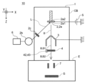
- FIG. 1 is a diagram schematically showing an electron gun 1 and an electron beam application device 10 according to an embodiment.
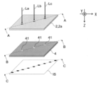
- FIG. 2 is a diagram for explaining an outline of how the electron gun 1 according to the embodiment forms multiple electron beams.
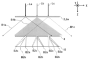
- FIG. 3 is a diagram for explaining an outline of how the electron gun 1 according to the embodiment forms multiple electron beams.
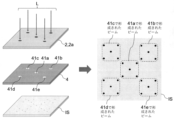
- FIG. 4 is a diagram for explaining an outline of how the electron gun 1 according to the embodiment forms multiple electron beams.
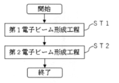
- FIG. 5 is a flow chart of a method for forming multiple electron beams.
- FIG. 6 is a diagram for explaining the outline of the second embodiment.
- FIG. 7 is a diagram showing an example in which the irradiation regions of the second electron beam B2 overlap.
- FIG. 8 is a diagram showing an example in which the irradiation area of the second electron beam B2 is missing.
- FIG. 9 is a diagram for explaining the outline of the third embodiment.
- FIG. 10 is a diagram for explaining the outline of the third embodiment.
- FIG. 11 is a diagram for explaining the outline of the third embodiment.
- FIG. 12 is a diagram for explaining the outline of the third embodiment.
- FIG. 13 is a diagram for explaining the outline of the third embodiment.
- FIG. 14 is a diagram for explaining the outline of the third embodiment.
- FIG. 15 is a diagram for explaining the outline of the third embodiment.
- FIG. 16 is a diagram for explaining the outline of the third embodiment.
- the Z direction is defined as the direction in which an electron beam formed by an electron source travels in a three-dimensional orthogonal coordinate system of X, Y, and Z axes. Note that the Z direction is, for example, the vertically downward direction, but the Z direction is not limited to the vertically downward direction.
- FIG. 1 is a diagram schematically showing an electron gun 1 and an electron beam application device 10 according to an embodiment.
- 2 to 4 are diagrams for explaining an outline of how the electron gun 1 according to the embodiment forms multiple electron beams.
- the electron gun 1 includes at least an electron source 2, an anode 3, and a multi-lens array 4.
- the electron gun 1 may optionally include a power supply 5 for generating an electric field between the electron source 2 and the anode 3, a control section 6 for controlling the electron source 2, and the like.
- the electron gun 1 may include an acceleration electrode and an acceleration power supply for accelerating the electron beam formed by the electron source 2 and the anode 3 .
- the counterpart device E of the electron beam application device 10 (the portion of the electron beam application device 10 excluding the electron gun 1) includes an electron beam deflection device 7.
- the electron beam deflector 7 is used to scan the irradiation target S with the second electron beam B2 formed by the electron gun 1 .
- the mating device E may be provided with known structural members according to the type of the electron beam application device 10 .
- the number of electron beams B formed by the electron gun 1 is one in order to show the outline of the electron gun 1 and the electron beam application apparatus 10 as a whole. The outline of the multiple electron beams in the electron gun 1 and the electron beam application apparatus 10 according to the embodiment will be described later in detail with reference to FIGS. 2 to 4.
- the electron source 2 is not particularly limited as long as it can form an electron beam B by generating electrons that can be emitted and extracting the generated electrons by an electric field formed between the anode 3, and a known electron source 2 is used. be able to.
- Examples of the electron source 2 include photocathode, field emitter, Schottky, and hot cathode.
- the electron beam irradiated to the multi-lens array 4 (before passing through the multi-lens array 4) is referred to as a first electron beam B1, and after passing through the multi-lens array 4 (multi-lens The electron beam emitted from the array 4) may be referred to as a second electron beam B2.
- the first electron beam B1 and the second electron beam B2 are not particularly distinguished, they may be simply referred to as an electron beam B in some cases.
- the photocathode 2a generates electrons that can be emitted in response to receiving the excitation light L emitted from the light source 2b.
- the principle by which the photocathode 2a generates electrons that can be emitted in response to receiving the excitation light L is known (see, for example, Japanese Patent No. 5808021).
- the photocathode 2a is formed of a substrate such as quartz glass or sapphire glass, and a photocathode film (not shown) adhered to the first surface 2a1 (the surface on the anode 3 side) of the substrate.
- the photocathode material for forming the photocathode film is not particularly limited as long as it can generate electrons that can be emitted by irradiation with the excitation light L.
- Materials requiring EA surface treatment include, for example, III-V group semiconductor materials and II-VI group semiconductor materials.
- the photocathode 2a can be produced by subjecting the photocathode material to EA surface treatment, and the photocathode 2a can select excitation light in the near-ultraviolet to infrared wavelength region according to the gap energy of the semiconductor.
- electron beam source performance quantitative yield, durability, monochromaticity, time response, spin polarization
- the application of the electron beam can be achieved by selecting the semiconductor material and structure.
- Materials that do not require EA surface treatment include, for example, simple metals such as Cu, Mg, Sm, Tb, and Y, alloys, metal compounds, diamond, WBaO, Cs 2 Te, and the like.
- a photocathode that does not require EA surface treatment may be produced by a known method (see, for example, Japanese Patent No. 3537779). The contents of US Pat. No. 3,537,779 are incorporated herein by reference in their entirety.
- the light source 2b is not particularly limited as long as it can form the electron beam B by irradiating the photocathode 2a with the excitation light L.
- the light source 2b may be, for example, a high output (watt class), high frequency (several hundred MHz), ultrashort pulse laser light source, relatively inexpensive laser diode, LED, or the like.
- the excitation light L to be irradiated may be either pulsed light or continuous light, and may be appropriately adjusted according to the purpose.
- the light source 2b is arranged outside the vacuum chamber CB, and the excitation light L is applied to the first surface 2a1 side of the photocathode 2a.
- the light source 2b may be arranged within the vacuum chamber CB.
- the excitation light L may be applied to the second surface 2a2 (the surface opposite to the anode 3) of the photocathode 2a.
- the anode 3 is not particularly limited as long as it can form an electric field with the electron source 2, and the anode 3 generally used in the field of electron guns may be used.
- electron beams B are formed by extracting electrons generated in the photocathode 2a by irradiation of the excitation light L, which can be emitted.
- the power supply 5 is connected to the photocathode 2a in order to form an electric field between the photocathode 2a and the anode 3, but a potential difference is generated between the photocathode 2a and the anode 3.
- the arrangement of the power supply 5 There is no particular restriction on the arrangement of the power supply 5.
- the photocathode 2a is linearly irradiated with three excitation lights La to Lc at different locations to form three first electron beams B1a to B1c (FIG. 2
- the illustration of the first electron beams B1a to B1c is omitted here (shown in FIG. 3).
- nine second electron beams B2a to B2c are formed (the second electron beams B2a to B2c are not shown in FIG. 2; they are shown in FIG. 3), and the nine second electron beams B2 are formed on the image plane IS. forming a focus.
- the image plane IS means a virtual plane on which the second electron beam B2 forms a focal point.
- the image plane IS may or may not match the surface of the irradiation target S.
- 3 is a cross-sectional view taken along lines AA, BB and CC of FIG. 2.
- FIG. An anode 3 exists between the photocathode 2a and the multi-lens array 4, but the illustration of the anode 3 is omitted in FIGS. 2 and 3 in order to avoid complicating the drawings.
- the incident first electron beams B1a to B1c are converged and focused on the image plane IS. It has the function of forming. Therefore, by irradiating the multi-lens array 4 having n lenses 41 with m first electron beams B1, a maximum of m ⁇ n second electron beams B2 can be formed. In order to form the maximum m ⁇ n second electron beams B2, each of the m first electron beams B1 should cover all the n lenses 41 of the multi-lens array 4. should be irradiated.
- the spread of the first electron beam B1 is adjusted, and the m first electron beams B1 are irradiated.
- the adjustment of the irradiation position of the beam B1, the arrangement of the n lenses 41, etc. may be adjusted by appropriately combining them.
- the spread of the first electron beam B1 can be adjusted by changing the strength of the electric field formed between the electron source 2 and the anode 3.
- FIG. Note that the electron gun 1 disclosed in the present application does not necessarily need to form the m ⁇ n second electron beams B2 from the m first electron beams B1. There may be a lens 41 that any first electron beam B1 cannot reach.
- the electron gun 1 disclosed in the present application irradiates the multi-lens array 4 having n lenses 41 with m first electron beams B1, thereby generating m+1 or more or n+1 or more second electron beams B1. It is sufficient if the electron beam B2 can be formed.
- the upper limits of m and n are not particularly limited as long as they are within the range in which the technical ideas disclosed in the present application can be achieved.
- advanced microfabrication technology is required, such as reducing the distance between the lenses 41 arranged in the multi-lens array 4, which leads to an increase in cost.
- the upper limits of m and n may be appropriately set in consideration of the merit of increasing the number of the second electron beams B2, the size of the apparatus, the cost, and the like.
- the number of first electron beams B1 may be greater than, equal to, or less than the number of lenses 41 (integer of 2 or more) as long as it is an integer of 2 or more.
- the arrangement of the first electron beams B1 (the positional relationship in which the m first electron beams B1 are emitted. In the example shown in FIGS. positional relationship of the lens 41) may be the same or different.
- the arrangement of the first electron beam B1 and the arrangement of the lens 41 when viewed from the electron source 2 in the direction of the multi-lens array 4 (Z direction), the first The arrangement of the electron beam B1 and the arrangement of the lens 41 may match or may be shifted.
- the arrangement of the first electron beam B1 and the arrangement of the lens 41 may have similar shapes with different sizes, although the shape when viewed in the Z direction is the same.
- the staggered arrangement includes, for example, the arrangement shown in FIG. 2 as described in (1) to (3) below.
- the arrangement of the first electron beam B1 and the arrangement of the lens 41 do not match when viewed in the Z direction.
- all of the m first electron beam B1 emission positions may not coincide with the lens 41, and some of the emission positions of the first electron beam B1 may coincide with the lens 41 .
- the center of rotation is not particularly limited, and the center of rotation may be a point where any one of the positions from which the first electron beam B1 is emitted coincides with the lens 41, or the position at which the first electron beam B1 is emitted and the lens 41. may be set as the center of rotation. (3) A combination of (1) and (2) above.
- the electron gun 1 irradiates the multi-lens array 4 having n lenses 41 with m first electron beams B1 to obtain m+1 or more or n+1 or more second electron beams B1.
- the arrangement of the first electron beam B1 and the arrangement of the lens 41 are not particularly limited as long as the electron beam B2 can be formed.
- five first electron beams B1 are formed by irradiating five excitation light beams L non-linearly (at the four corners of the square and at the middle point of the square). (The illustration of the first electron beam B1 is omitted).
- Each of the five first electron beams B1 formed is incident on each of the five lenses 41a to 41e provided in the multi-lens array 4.
- five second electron beams B2 are formed from each of the lenses 41a to 41e, so that a total of 25 second electron beams B2 are formed. be.
- the first electron beam B1 and the lens 41 may be arranged to be shifted as described above.
- the forming method is not particularly limited as long as at least two first electron beams B1 are formed.
- the electron source 2 is a photocathode 2a
- the photocathode 2a may be irradiated with m excitation lights L as shown in FIGS.
- m light sources 2b may be used.
- a light splitter 2c such as a liquid crystal shutter is arranged between the single light source 2b and the photocathode 2a, and the excitation light emitted from the single light source 2b is separated by the light splitter 2c. You may divide L into any desired number.
- the electron beam B may be emitted from the photocathode 2a, and the emitted electron beam B may be split using an aperture array or the like to form m first electron beams B1.
- an aperture array formed of a metal plate or the like may be used.
- an aperture array with a blanking function for example, an aperture array with a deflection function, an electrostatic lens array
- FIGS. 1 to 4 an example using the photocathode 2a as the electron source 2 is explained, but as described above, a known electron source 2 such as a field emitter, Schottky, hot cathode, etc. may be used. good. In that case, the light source 2b and the optical splitter 2c shown in FIG. 1 are unnecessary. Field emitters and Schottky can also be arrayed side by side. Therefore, in the case of the field emitter and the Schottky, m first electron beams B1 may be emitted from an array of elements. may be divided to form m first electron beams B1.
- a hot cathode is large in size as an electron source 2 compared to a photocathode, a field emitter, and a Schottky. Therefore, although it is technically possible to arrange two or more hot cathodes, the size of the electron gun 1 may increase. Therefore, when a hot cathode is used as the electron source 2, the electron beam B is emitted first, and the emitted electron beam B is split using an aperture array or the like from the viewpoint of convenience rather than from a technical point of view. to form the first electron beam B1.
- anode 3 one commonly used in the field of the electron gun 1 may be used.
- the multi-lens array 4 is not particularly limited as long as it has the function of converging the m first electron beams B1 incident on the respective lenses 41 and forming m focal points on the image plane IS.
- the charged particle beam lens array described in JP-A-2013-30567, JP-A-2014-53408, etc. can be used. All matters described in JP-A-2013-30567 and JP-A-2014-53408 are incorporated herein by reference.
- a controller 6 for controlling the light source 2b is provided.
- the control unit 6 can control the number of first electron beams B1 to be formed by controlling which light source 2b emits the excitation light L.
- the controller 6 may control the optical splitter 2c to control the number of the first electron beams B1 to be formed.
- the photocathode 2a has a feature of emitting an electron beam B from a position where the excitation light L is received.
- the controller 6 may control the position of the excitation light L received by the photocathode 2a.
- the irradiation position of the excitation light L is changed, the incident angle of each of the first electron beams B1 entering the multi-lens array 4 can be adjusted. Therefore, even after the electron gun 1 is assembled, in other words, even after the multi-lens array 4 is set up, the controller 6 adjusts the irradiation number and/or the irradiation position of the excitation light L so that the image plane The number and positional relationship of focal points formed on the IS can be adjusted. Further, the control unit 6 may control the intensity of the excitation light L, or may control the excitation light L so that the photocathode 2a is irradiated with the excitation light L as continuous light or pulsed light.
- the controller 6 may control from which element constituting the array the electron beam B is emitted.
- the elements are arranged in the row direction and the column direction, the number and/or the emission position of the elements for emitting the electron beam B can be adjusted, so that the same effects as those of the photocathode 2a can be obtained.
- control unit 6 may control from which hot cathode the electron beam B is emitted.
- a member for example, an electrostatic lens, etc.
- the controller 6 may control the number and locations of the first electron beams B1 split from the electron beam B by controlling .
- the electron beam application device 10 equipped with the electron gun 1 includes a known device equipped with an electron gun.
- a known device equipped with an electron gun for example, free electron laser accelerator, electron microscope, electron beam holography device, electron beam drawing device, electron beam diffraction device, electron beam inspection device, electron beam metal additive manufacturing device, electron beam lithography device, electron beam processing device, electron beam curing devices, electron beam sterilizers, electron beam sterilizers, plasma generators, atomic element generators, spin-polarized electron beam generators, cathodoluminescence devices, reverse photoelectron spectroscopy devices, and the like.
- the second electron beam B2 formed by the electron gun 1 disclosed in the present application may be appropriately adjusted according to the type of the electron beam application device 10.
- the electron beam application apparatus 10 is a scanning electron microscope or a scanning electron beam inspection apparatus
- the sample is imaged by scanning a plurality of line-shaped second electron beams B2 formed as shown in FIG. You can save time and inspection time.
- a plurality of second electron beams B2 are formed in a plane as shown in FIG. 4, it can be used for transmission electron microscopes, electron beam sterilizers, electron beam sterilizers, and the like. It can also be used for electron beam drawing devices (mask drawing devices, direct drawing devices), electron beam metal additive manufacturing devices (metal 3D printers), and the like, regardless of scanning or non-scanning.
- FIG. 5 is a flow chart of a method for forming multiple electron beams.
- a method of forming a multi-electron beam includes a first electron beam forming step (ST1) and a second electron beam forming step (ST2).
- first electron beam forming step (ST1) an electric field is formed between an electron source 2 that generates electrons that can be emitted and an anode 3, thereby generating m electron beams (m is an arbitrary value of 2 or more) from the electron source 2. (integer of ) of the first electron beam B1 is emitted.
- m is an arbitrary value of 2 or more
- first electron beams B1 may be formed.
- a known electron source such as a photocathode, a field emitter, a Schottky, or a hot cathode may be used as described in the embodiment of the electron gun 1.
- FIG. When a plurality of hot cathodes are used as the electron source 2, the electron gun 1 may become large. Therefore, when a hot cathode is used as the electron source 2, first, an electron beam B is extracted from the hot cathode, and the extracted electron beam B is divided into m (m is an arbitrary integer of 2 or more) first electrons. It is preferred to form beam B1.
- the m first electron beams B1 are irradiated to the multi-lens array 4 having n lenses 41 (where n is an arbitrary integer equal to or greater than 2). m ⁇ n second electron beams B2 are formed.
- the electron gun 1 disclosed in the present application, the electron beam application device 10 equipped with the electron gun 1, and the method for forming a multi-electron beam (hereinafter, "the electron gun 1, the electron beam application device 10, and the method for forming a multi-electron beam” are summarized. described as “electron gun, etc.”) has the following effects. (1) When the number of the second electron beams B2 formed on the image plane IS (to be irradiated to the irradiation target S) is the same, the electron gun or the like irradiates the multi-lens array 4 with m first electron beams B1. , the number of lenses 41 included in the multi-lens array 4 can be made smaller than in Patent Document 1.
- the electron gun or the like disclosed in the present application causes m first electron beams B1 having different emission positions to be incident on the lens 41, thereby narrowing the distance between the lenses 41.
- a second electron beam B2 can be focused on the image plane IS at intervals.
- the interval between the lenses 41 of the electron gun 1 can be made wider than the hole provided in the lens 7 described in Japanese Unexamined Patent Application Publication No. 2002-200010. Therefore, manufacturing of the multi-lens array 4 is facilitated. Further, since the distance between the lenses 41 can be increased, the size of the lenses 41 can be increased. When the size of the lens 41 is increased, the beam current of the electron beam B1 passing through each lens 41 can be increased (brightness is increased). (3) Assume an embodiment in which the electron source 2 forms m first electron beams B1 without using an aperture array or the like.
- any one of a photocathode, a field emitter, a Schottky, and a hot cathode may be used. 1 size can be reduced. Also, in the field emitter or Schottky, when the elements are arranged in an array, as with the lens 41 of the multi-lens array 4, as the number of elements increases, defects in one of the elements forming the array during manufacture or use will increase. more likely to occur.
- the photocathode 2a can be manufactured as one member by bonding the photocathode film to the substrate.
- the photocathode 2a when the photocathode 2a is used for the electron source 2 that forms the plurality of first electron beams B1, the size of the electron gun and the like can be reduced, and the probability of defects occurring during manufacture or use is reduced. (4) Further, the photocathode 2a can easily change the number and arrangement of the emitted first electron beams B1 by adjusting the number and irradiation position of the excitation light L.
- the number and the incident angles of the first electron beams B1 incident on the multilens array 4 are can be adjusted to adjust the number and arrangement of the second electron beams B2 formed on the image plane IS (to irradiate the irradiation target S).
- FIG. 6 is a diagram for explaining the outline of the second embodiment.
- the electron gun 1 disclosed in the present application irradiates a lens array 4 having n lenses 41 with m first electron beams B1, thereby generating m ⁇ n electron beams at maximum. number of second electron beams B2 can be formed on the image plane IS.
- the inventors of the present invention have investigated the emission positions when the m first electron beams B1 are emitted (hereinafter sometimes referred to as "first electron beam emission positions") and the lenses included in the multi-lens array 4. 41 positional relationship and .
- first electron beam emission positions the positional relationship between the first electron beam emission position and the lens 41 provided in the multi-lens array 4 when viewed in the Z direction
- this positional relationship may be hereinafter referred to as "relative positional relationship”
- the second electron beam B2 formed on the image plane IS can be controlled to have a suitable arrangement by controlling.
- An electron gun 1 according to the second embodiment includes a controller 6 as a component.
- first embodiment embodiment of electron gun and electron beam application device (hereinafter referred to as "first embodiment") )). Therefore, in the second embodiment, the points different from the first embodiment will be mainly described, and repetitive descriptions of items already described in the first embodiment will be omitted. Therefore, it is needless to say that the items already explained in the first embodiment can be adopted in the second embodiment even if they are not explicitly explained in the second embodiment.
- FIG. 6A when the arrangement of the first electron beam emission positions is defined as the emission arrangement and the arrangement of the lenses 41 provided in the multi-lens array 4 is defined as the lens arrangement, the emission arrangement as shown in FIG. And the lens arrangement is the same (same shape), and when the injection arrangement seen in the Z direction is used as a reference, the lens arrangement seen in the Z direction is the same as the injection arrangement (overlap).
- a second electron beam B2 formed on the surface IS is shown.
- first electron beam emission position means a position where m first electron beams B1 are emitted.
- the position where the electrons of the electron source 2 are extracted is the injection position.
- an electron beam splitting device such as an aperture array to form m first electron beams B1
- the position of the m first electron beams B1 emitted from the electron beam splitting device is the emission position.
- FIG. 6B when the injection arrangement seen in the Z direction is used as a reference, the lens arrangement is adjusted with the center of the injection arrangement as the rotation axis so that the lens arrangement seen in the Z direction does not become the same arrangement as the injection arrangement.
- It shows the second electron beam B2 formed on the image plane IS when arranged in a rotated position.
- FIG. 6(3) shows the second electron beam B2 formed on the image plane IS when the lens arrangement is further rotated on the basis of the injection arrangement from the example shown in FIG. 6(2).
- the second electron beam B2 formed on the image plane IS is arranged by rotating the lens arrangement with reference to the emission arrangement viewed in the Z direction. changes. More specifically, in the example shown in FIG.
- the individual regions of the second electron beam B2 formed by passing through the individual lenses 41 (a to e) (hereinafter referred to as "B2 individual lens regions") ) and the gap between the regions (the portion indicated by the circle in FIG. 6(1)) is approximately the same size as the B2 individual lens region.
- the gap between the B2 individual lens regions (indicated by the circle in FIG. 6(3) part) becomes smaller.
- the electron beam application device is, for example, a non-scanning electron beam sterilizer or a non-scanning electron beam sterilizer, the smaller the gap between the B2 individual lens regions, the less uneven heating. Therefore, sterilization or sterilization efficiency can be increased.
- the degree to which the lens arrangement is rotated about the center of the injection arrangement may be appropriately set according to the purpose.
- FIG. 6 is an example in which the injection arrangement and the lens arrangement seen in the Z direction are the same (same shape).
- the injection arrangement and the lens arrangement are similar arrangements (similar shapes), and when the injection arrangement seen in the Z direction is used as a reference, the lens arrangement seen in the Z direction is not similar to the injection arrangement. , may be arranged at a position rotated about the center of the injection arrangement as the rotation axis. Further alternatively, the injection arrangement and lens arrangement may not be the same or similar as long as the gap between the B2 individual lens regions is reduced by changing the relative positional relationship of the injection arrangement and lens arrangement.
- the control unit 6 may perform control so that the relative positional relationship becomes a preset positional relationship.
- the relative positional relationship may be set when assembling the electron gun 1 so that the positional relationship is set in advance. In other words, after the electron gun 1 is assembled, it can be fixed so that the relative positional relationship does not change. However, after assembling the electron gun 1, fine adjustment may be necessary. Therefore, after the electron gun 1 is assembled, it is desirable that the control section 6 can be controlled so as to adjust the relative positional relationship.
- the controller 6 may control the position of the excitation light L received by the photocathode 2a. If the electron source 2 is a field emitter or Schottky, the controller 6 may control the field emitter or Schottky element that emits the first electron beam B1.
- the electron gun 1 includes a rotation mechanism 42 that rotates the multi-lens array 4 about the Z direction, and the controller 6 controls the rotation mechanism 42 to control the relative positional relationship.
- the rotation mechanism 42 is not particularly limited as long as it can rotate the multi-lens array 4 .
- a gear that engages with the outer periphery of the multi-lens array 4 may be provided, and the gear may be rotated by a drive source such as a motor.
- the controller 6 may control both the electron source 2 and the rotating mechanism 42 of the multi-lens array 4 .
- the controller 6 controls the rotating mechanism 42 of the multi-lens array 4 to You can control the relative positional relationship.
- a rotating mechanism for rotating the electron beam splitting device hereinafter sometimes referred to as a "splitting device rotating mechanism"
- the controller 6 controls the splitting device rotating mechanism. By doing so, the relative positional relationship may be controlled.
- the dividing device rotating mechanism may have a mechanism similar to the rotating mechanism 42 .
- the controller 6 may control both the rotating mechanism 42 and the dividing device rotating mechanism.
- the electron gun 1 may include a moving mechanism 43 for moving the multi-lens array 4 in the Z direction, and the control unit 6 may control the moving mechanism 43 .
- the moving mechanism 43 is not particularly limited as long as it can move the multi-lens array 4 in the Z direction.
- a drive source such as a rack and pinion mechanism and a motor may be provided.
- the electron gun 1 When the control unit 6 controls the rotation mechanism 42 that rotates the multi-lens array 4, the electron gun 1 needs to employ a configuration in which the rotation mechanism 42 is used.
- the controller 6 controls the photocathode, field emitter or Schottky
- the rotating mechanism 42 for rotating the multi-lens array 4 is not required, and the electron gun 1 can be simplified. Therefore, it is more preferable for the controller 6 to control the photocathode, field emitter or Schottky.
- the photocathode has the feature of being able to rapidly emit an electron beam from any location where the excitation light L is received.
- the relative positional relationship is controlled to be a preset positional relationship and/or the relative positional relationship fine-tuning can be performed quickly.
- the electron gun 1 By controlling the relative positional relationship, the electron gun 1 according to the second embodiment has the effect that the second electron beam B2 formed on the image plane IS can be controlled to have a suitable arrangement.
- FIG. 7 is a diagram showing an example in which the irradiation regions of the second electron beam B2 overlap.
- FIG. 8 is a diagram showing an example in which the irradiation area of the second electron beam B2 is missing.
- 9 to 16 are diagrams for explaining the outline of the third embodiment.
- the electron gun 1 is installed in a scanning electron beam application apparatus 10, for example.
- the second electron beam B2 can be formed linearly on the image plane IS, by scanning the formed linear second electron beam B2 with the electron beam deflection device 7,
- the irradiation target S can be irradiated with the second electron beam B2 without duplication or loss.
- the second electron beam B2 is formed non-linearly on the image plane IS.
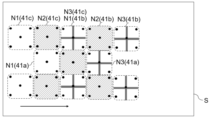
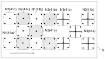
- N1 (41a), N1 (41b) , N1 (41c).) are formed on the image plane IS, and the illumination target S is illuminated.
- N2 (41b), N2 (41c) is irradiated to the irradiation target S.
- the second electron beam B2 with which the irradiation target S is irradiated does not overlap.
- the second electron beam B2 is repeatedly irradiated to any region after the n-th time, such as N2 (41b) for the fourth time, N3 (41B) for the fifth time, and so on.
- the area irradiated with the second electron beam B2 formed on the image plane is defined as the second electron beam irradiation area.
- the second electron beam irradiation area has a shape that can completely fill the irradiation target S without loss or overlap.
- the second electron beam irradiation area is non-linear. In other words, the second electron beam B2 is not aligned linearly.
- the shape in which the second electron beam irradiation area can completely cover the irradiation target S without loss or overlap is obtained by adjusting the injection arrangement and the lens arrangement to, for example, three or more odd-numbered points at equal intervals in a straight line, the four corners and the center of a square. , six corners and the center of a regular hexagon. Note that the above example is a typical example, and other arrangements may be used as long as the third embodiment can be implemented.
- the exit arrangement and lens arrangement are of the same size or similar shape when viewed in the Z direction.
- the relationship for the second electron beam irradiation area to fill the irradiation target S without loss and overlap will be described.
- the case where the injection arrangement and lens arrangement are four corners and the center of a square or six corners and the center of a regular hexagon will be described.
- a first electron beam B1 emitted from the electron source 2 passes through a lens provided in a multi-lens array (MLA) 4, and a second electron beam B2 is formed on the image plane IS. be done.
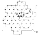
- the position vector P of the beam on the image plane IS can be expressed by the following equation (1).
- central axis 10 is the direction connecting the injection position at the center of the injection arrangement and the lens arranged at the center of the lens arrangement (hereinafter sometimes referred to as "central axis"). More specifically, when the injection arrangement and lens arrangement are four corners and the center of a square, the directions are the directions connecting the centers, and when the six corners and the center of a regular hexagon are the directions connecting the centers.
- central axis the direction connecting the injection position at the center of the injection arrangement and the lens arranged at the center of the lens arrangement
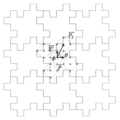
- FIG. 11 is a view of the image plane IS in the Z direction when the exit arrangement and lens arrangement are the six corners and the center of a regular hexagon.
- the meanings of symbols in FIG. 11 are as described above.
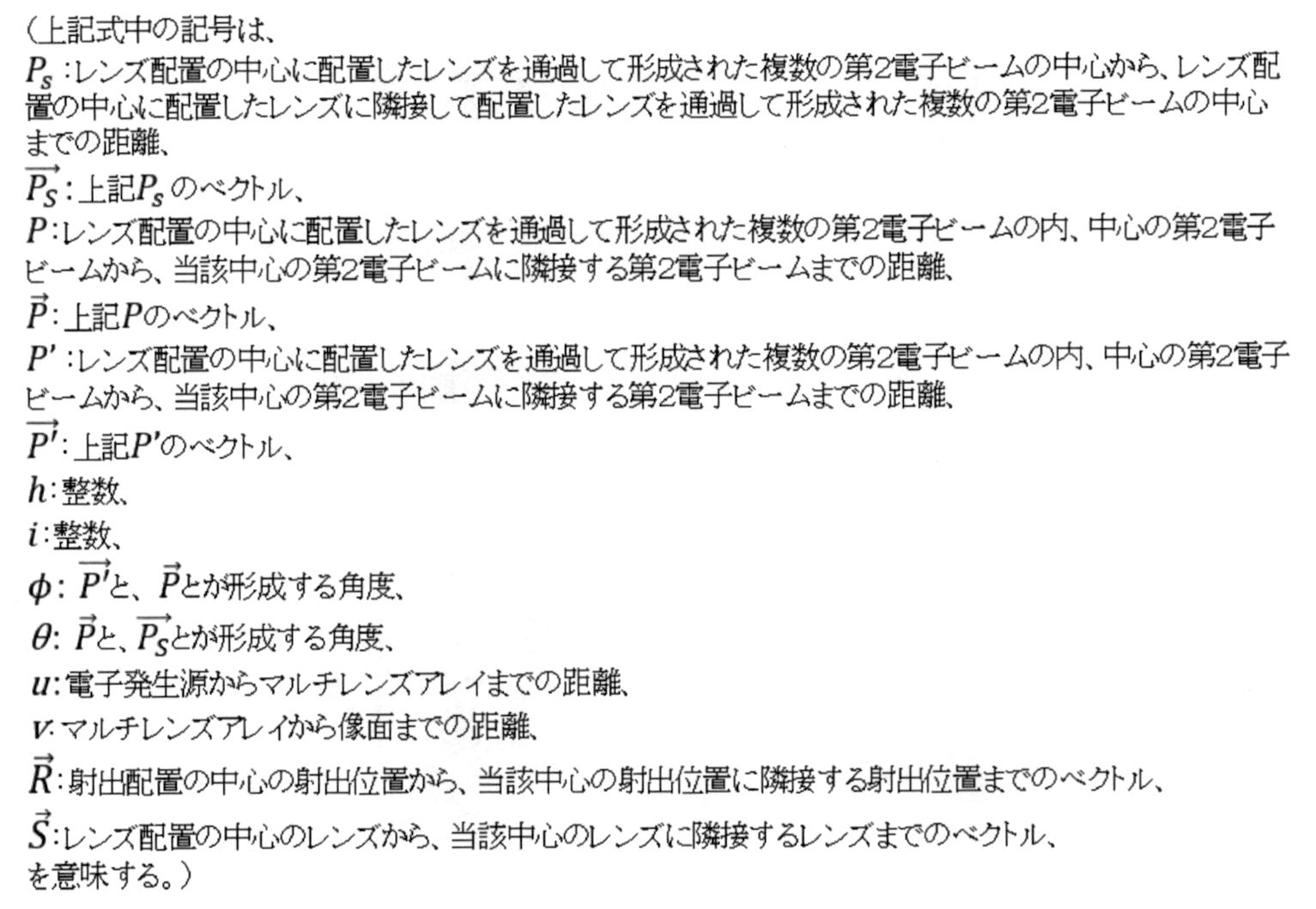
- the second electron beam B2 formed on the image plane IS can be represented by the basis vectors shown in the following equation (2).
- Equation (3) is derived from Equation (2), and considering the relationship of Equation (4), the angle ⁇ formed by vector P and vector Ps can be expressed by Equation (5).
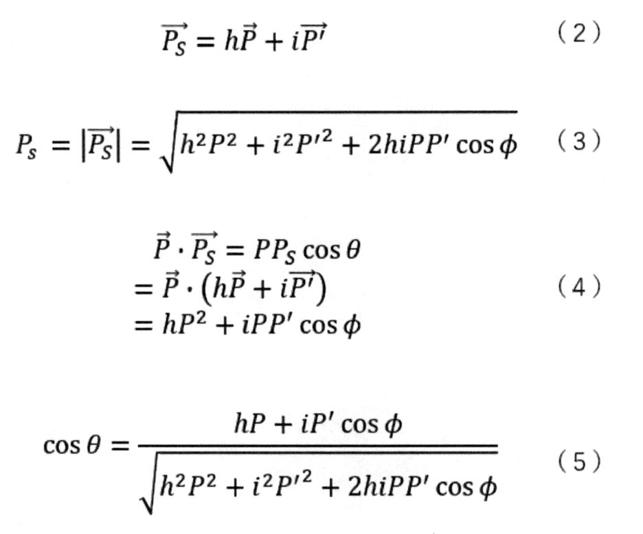
- the absolute value of the vector R is expressed by the following equation (6).
- the absolute value of the vector S can be expressed by the following equation (7).
- the distance u from the electron source 2 to the multi-lens array 4 the distance v from the multi-lens array 4 to the image plane IS, the first electron beam B1
- design information such as the number of lenses
- the lens arrangement seen in the Z direction is rotated from the same or similar arrangement as the injection arrangement by rotating the center of the injection arrangement.
- the angle ⁇ to rotate about axis C can be calculated.
- Fig. 12 shows the arrangement based on the numerical values obtained by the above calculation.
- 49 second electron beams B2 can be formed at intervals of 100 ⁇ m.
- the shapes of the 49 second electron beams B2 formed are divided regions S1, S2, . It is a shape that can irradiate Therefore, by using the electron gun 1 designed with the electron source 2 and the multi-lens array 4 as shown in FIG. 12, the irradiation target S can be scanned with the second electron beam B2 without missing or overlapping irradiation.
- Fig. 14 shows the arrangement based on the numerical values obtained by the above calculation.
- 25 second electron beams B2 can be formed at intervals of 100 ⁇ m.
- the shapes of the 25 second electron beams B2 thus formed correspond to divided regions of the same shape that can fill the irradiation target S shown in FIG. 13 without loss or overlap.
- Second electron beams B2 are linearly formed on the image plane IS at regular intervals.
- FIG. 15 when the lens arrangement seen in the Z direction is based on the injection arrangement seen in the Z direction, when the lens arrangement seen in the Z direction is arranged at a position rotated around the center of the injection arrangement as a rotation axis, the position shown in FIG.
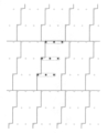
- a parallelogram-shaped second electron beam irradiation area is formed on the image plane IS.
- the size of the parallelogram formed varies with the angle of rotation, the resulting shape remains a parallelogram.
- a parallelogram is a shape that can completely cover the irradiation target without loss or duplication. Therefore, when the injection arrangement and lens arrangement are three or more odd-numbered points that are equally spaced linearly, the rotation angle may be any angle, and the interval for scanning the second electron beam irradiation area is adjusted according to the rotation angle. do it.
- the number of odd points is not particularly limited as long as it is 3 or more, and examples thereof include 5, 7, 9, 11, 13, 15, and the like. The upper limit of the odd number of points is not particularly limited in principle.
- the size of the irradiation target S, the size of the second electron beam B2, and the like may be taken into consideration when setting the value as appropriate.
- the emission position of the first electron beam B1 is set at an interval (center-to-center distance) of 315 ⁇ m (vector R) from the center and central axis of the electron source 2, and the lens is positioned from the center and central axis of the multi-lens array (MLA) 4. They are arranged at intervals (center-to-center distance) of 156 ⁇ m (vector S).
- the above description is for the case where the first electron beam emission position is formed in the electron source 2 .
- the electron source 2 can be read as the electron beam splitting device in the above description.
- the sizes (preferably diameters) of the first electron beam B1, the second electron beam B2, and the lens 41 shown in the drawings are only schematic. The sizes of the first electron beam B1, the second electron beam B2, and the lens 41 may be appropriately adjusted within the objective ranges of the second and third embodiments.
- the third embodiment is particularly useful for scanning electron beam application apparatus 10.
- the scanning electron beam application apparatus 10 include, but are not limited to, a scanning electron microscope, an electron beam inspection apparatus, a scanning transmission electron microscope, and the like.
- the third embodiment may be applied to a non-scanning electron beam application apparatus 10.
- the third embodiment has the following effects in addition to the effects described in the second embodiment.
- the direction from the electron source 2 to the multi-lens array 4 is defined as the Z direction, and the emission position when the first electron beam B1 is emitted from the electron source 2 is
- the first electron beam emission position is defined, the positional relationship between the first electron beam emission position and the lenses of the multi-lens array when viewed in the Z direction is controlled so as to achieve a preset positional relationship.
- first embodiment of method unlike the above (embodiment of method for forming multiple electron beams (hereinafter sometimes referred to as "first embodiment of method")), other points are the same as the first embodiment of method. is. Therefore, in the second embodiment of the method for forming multiple electron beams, the points different from the first embodiment of the method will be mainly described, and the description of the items already explained in the first embodiment of the method will be repeated. are omitted. Therefore, even if not explicitly explained in the second embodiment of the method for forming multiple electron beams, it goes without saying that the matters already explained in the first embodiment of the method can be adopted.
- the direction from the electron source 2 to the multi-lens array 4 is defined as the Z direction, and the emission position when the first electron beam B1 is emitted from the electron source 2. is defined as the first electron beam emission position, the positional relationship between the first electron beam emission position and the lenses of the multi-lens array when viewed in the Z direction is controlled so as to be a preset positional relationship.
- the second and third embodiments are the same as those described in the second and third embodiments. Therefore, a detailed description of each step included in the second embodiment of the method for forming multiple electron beams will be omitted since they have already been substantially described in the second and third embodiments.
- the injection arrangement and the lens arrangement are The formed multi-electron beam may be scanned after controlling the arrangement described in the third embodiment.
- the second embodiment of the method for forming multiple electron beams has the same effects as those described in the second and third embodiments.
- the electron gun, electron beam application apparatus, and multi-electron beam formation method disclosed in the present application can improve the yield of manufacturing a multi-lens array and reduce the running cost of the electron gun or electron beam application apparatus. Therefore, it is useful for industries dealing with multiple electron beams.
- Electron beam deflector 10 Electron beam applying device B... Electron beam B1, B1a to B1c... th 1 electron beam, B2, B2a to B2c... second electron beam, CB... vacuum chamber, E... partner device, IS... image plane, L, La to Lc... excitation light, S... irradiation target
Landscapes
- Chemical & Material Sciences (AREA)
- Analytical Chemistry (AREA)
- Physics & Mathematics (AREA)
- Engineering & Computer Science (AREA)
- Plasma & Fusion (AREA)
- Optics & Photonics (AREA)
- Electron Sources, Ion Sources (AREA)
- Electron Beam Exposure (AREA)
Abstract
Description
前記電子発生源との間で電界を形成することができ、形成した電界により前記放出可能な電子を引き出し、電子ビームを形成するアノードと、
マルチレンズアレイと、
を含む、電子銃であって、
前記マルチレンズアレイに照射される電子ビームを第1電子ビームと規定した時に、前記第1電子ビームはm個(mは2以上の任意の整数)形成され、
前記マルチレンズアレイはn個(nは2以上の任意の整数)のレンズを具備し、
前記マルチレンズアレイから射出する電子ビームを第2電子ビームと規定した時に、前記マルチレンズアレイが具備する個々のレンズには異なる位置から照射された前記第1電子ビームが入射することで、前記第2電子ビームを最大m×n個形成できる
電子銃。
(2)前記電子発生源が、フォトカソードである
上記(1)に記載の電子銃。
(3)前記電子発生源が、フィールドエミッタまたはショットキーである
上記(1)に記載の電子銃。
(4)前記電子発生源が、熱陰極である
上記(1)に記載の電子銃。
(5)制御部を更に含み、該制御部は、
前記電子発生源から前記マルチレンズアレイの方向をZ方向と規定し、前記m個の第1電子ビームが射出する際の射出位置を第1電子ビーム射出位置と規定した時に、
前記Z方向に見た時の前記第1電子ビーム射出位置および前記マルチレンズアレイが具備するレンズの位置関係が、予め設定した位置関係となるように制御できる
上記(1)~(4)の何れか一つに記載の電子銃。
(6)前記Z方向を回転軸として、前記マルチレンズアレイを回転する回転機構を更に含み、
前記制御部が、前記回転機構を制御する
上記(5)に記載の電子銃。
(7)前記Z方向を移動方向に、前記マルチレンズアレイを移動する移動機構を更に含み、
前記制御部が、前記移動機構を制御する
上記(5)に記載の電子銃。
(8)前記第1電子ビーム射出位置の配置を射出配置と規定し、前記マルチレンズアレイが具備するレンズの配置をレンズ配置と規定した時に、
前記射出配置および前記レンズ配置は、同一または相似した配置であり、
前記Z方向に見た前記射出配置を基準とした時に、前記Z方向に見た前記レンズ配置が、前記射出配置と同一または相似した配置とならないように、前記射出配置の中心を回転軸として回転した位置に配置される
上記(5)に記載の電子銃。
(9)前記射出配置および前記レンズ配置が、
直線状の等間隔の3以上の奇数点、
正方形の4隅と中心、および、
正六角形の6隅と中心、
からなる群から選択した何れか一つである
上記(8)に記載の電子銃。
(10)上記(1)~(4)のいずれか一つに記載の電子銃を含む電子線適用装置であって、
電子線適用装置は、
自由電子レーザー加速器、
電子顕微鏡、
電子線ホログラフィー装置、
電子線描画装置、
電子線回折装置、
電子線検査装置、
電子線金属積層造形装置、
電子線リソグラフィー装置、
電子線加工装置、
電子線硬化装置、
電子線滅菌装置、
電子線殺菌装置、
プラズマ発生装置、
原子状元素発生装置、
スピン偏極電子線発生装置、
カソードルミネッセンス装置、または、
逆光電子分光装置
である
電子線適用装置。
(11)マルチ電子ビームの形成方法であって、該形成方法は、
第1電子ビーム形成工程と、
第2電子ビーム形成工程と、
を含み、
前記第1電子ビーム形成工程は、
放出可能な電子を生成する電子発生源およびアノードとの間で電界を形成することで、電子発生源からm個(mは2以上の任意の整数)の第1電子ビームを射出、または、
放出可能な電子を生成する電子発生源およびアノードとの間で電界を形成することで電子ビームを引き出し、引き出した電子ビームを分割することでm個(mは2以上の任意の整数)の第1電子ビームを形成し、
前記第2電子ビーム形成工程は、
前記m個の第1電子ビームを、n個(nは2以上の任意の整数)のレンズを具備したマルチレンズアレイに照射し、前記マルチレンズアレイが具備する個々のレンズには異なる位置から照射された前記第1電子ビームが入射することで、最大m×n個の第2電子ビームを形成する
マルチ電子ビームの形成方法。
(12)前記電子発生源が、フォトカソード、フィールドエミッタ、および、ショットキーからなる群から選択した何れか一つである
上記(11)に記載のマルチ電子ビームの形成方法。
(13)前記電子発生源が、熱陰極であり、
前記第1電子ビーム形成工程が、
放出可能な電子を生成する電子発生源およびアノードとの間で電界を形成することで電子ビームを引き出し、引き出した電子ビームを分割することでm個(mは2以上の任意の整数)の第1電子ビームを形成する
上記(11)に記載のマルチ電子ビームの形成方法。
(14)前記電子発生源から前記マルチレンズアレイの方向をZ方向と規定し、前記電子発生源から前記第1電子ビームが射出する際の射出位置を第1電子ビーム射出位置と規定した時に、
前記Z方向に見た時の前記第1電子ビーム射出位置および前記マルチレンズアレイが具備するレンズの位置関係が、予め設定した位置関係となるように制御される
上記(11)~(13)の何れか一つに記載のマルチ電子ビームの形成方法。
(15)前記第1電子ビーム射出位置の配置を射出配置と規定し、前記マルチレンズアレイが具備するレンズの配置をレンズ配置と規定した時に、
前記射出配置および前記レンズ配置は、同一または相似した配置であり、
前記Z方向に見た前記射出配置を基準とした時に、前記Z方向に見た前記レンズ配置が、前記射出配置と同一または相似した配置とならないように、前記射出配置の中心を回転軸として回転した位置に配置される
上記(14)に記載のマルチ電子ビームの形成方法。
(1)放出可能な電子を生成する電子発生源と、
前記電子発生源との間で電界を形成することができ、形成した電界により前記放出可能な電子を引き出し、電子ビームを形成するアノードと、
マルチレンズアレイと、
制御部と、
を含む、電子銃であって、
前記マルチレンズアレイに照射される電子ビームを第1電子ビームと規定した時に、前記第1電子ビームはm個(mは2以上の任意の整数)形成され、
前記マルチレンズアレイはn個(nは2以上の任意の整数)のレンズを具備し、
前記マルチレンズアレイから射出する電子ビームを第2電子ビームと規定した時に、
前記マルチレンズアレイが具備する個々のレンズには異なる位置から照射された前記第1電子ビームが入射することで、前記第2電子ビームを最大m×n個形成でき、
前記制御部は、
前記電子発生源から前記マルチレンズアレイの方向をZ方向と規定し、前記m個の第1電子ビームが射出する際の射出位置を第1電子ビーム射出位置と規定した時に、
前記Z方向に見た時の前記第1電子ビーム射出位置および前記マルチレンズアレイが具備するレンズの位置関係が、予め設定した位置関係となるように制御できる、
電子銃。
(2)前記電子発生源が、フォトカソードであり、
前記制御部が、前記フォトカソードが受光する励起光の位置を制御する、
上記(1)に記載の電子銃。
(3)前記電子発生源が、フィールドエミッタまたはショットキーであり、
前記制御部が、前記フィールドエミッタまたはショットキーから前記第1電子ビームを射出する素子を制御する、
上記(1)に記載の電子銃。
(4)前記Z方向を回転軸として、前記マルチレンズアレイを回転する回転機構を更に含み、
前記制御部が、前記回転機構を制御する、
上記(1)~(3)の何れか一つに記載の電子銃。
(5)前記Z方向を移動方向に、前記マルチレンズアレイを移動する移動機構を更に含み、
前記制御部が、前記移動機構を制御する、
上記(1)~(4)の何れか一つに記載の電子銃。
(6)前記第1電子ビーム射出位置の配置を射出配置と規定し、前記マルチレンズアレイが具備するレンズの配置をレンズ配置と規定した時に、
前記射出配置および前記レンズ配置は、同一または相似した配置であり、
前記Z方向に見た前記射出配置を基準とした時に、前記Z方向に見た前記レンズ配置が、前記射出配置と同一または相似した配置とならないように、前記射出配置の中心を回転軸として回転した位置に配置される、
上記(1)~(5)の何れか一つに記載の電子銃。
(7)前記射出配置および前記レンズ配置が、
直線状の等間隔の3以上の奇数点、
正方形の4隅と中心、および、
正六角形の6隅と中心、
からなる群から選択した何れか一つである、
上記(6)に記載の電子銃。
(8)像面に形成される前記第2電子ビームが照射される領域を第2電子ビーム照射領域と規定した時に、
前記第2電子ビーム照射領域は、照射対象を欠損および重複なく埋め尽くすことができる形状である、
上記(7)に記載の電子銃。
(9)前記射出配置および前記レンズ配置が、正方形の4隅と中心、または、正六角形の6隅と中心であり、
前記射出配置および前記レンズ配置が以下の式を満たし、
前記Z方向に見た前記射出配置を基準とした時に、前記Z方向に見た前記レンズ配置を前記射出配置と同一または相似した配置から前記射出配置の中心を回転軸として回転した角度が、以下の式においてθで表される、

(10)上記(9)に記載の電子銃を含む電子線適用装置であって、
前記電子線適用装置が、
走査電子顕微鏡、
電子線検査装置、または、
走査型透過電子顕微鏡、
である、
電子線適用装置。
(11)マルチ電子ビームの形成方法であって、該形成方法は、
第1電子ビーム形成工程と、
第2電子ビーム形成工程と、
を含み、
前記第1電子ビーム形成工程は、
放出可能な電子を生成する電子発生源およびアノードとの間で電界を形成することで、電子発生源からm個(mは2以上の任意の整数)の第1電子ビームを射出し、
または、
放出可能な電子を生成する電子発生源およびアノードとの間で電界を形成することで電子ビームを引き出し、引き出した電子ビームを分割することでm個(mは2以上の任意の整数)の第1電子ビームを形成し、
前記第2電子ビーム形成工程は、
前記m個の第1電子ビームを、n個(nは2以上の任意の整数)のレンズを具備したマルチレンズアレイに照射し、前記マルチレンズアレイが具備する個々のレンズには異なる位置から照射された前記第1電子ビームが入射することで、最大m×n個の第2電子ビームを形成し、
前記電子発生源から前記マルチレンズアレイの方向をZ方向と規定し、前記電子発生源から前記第1電子ビームが射出する際の射出位置を第1電子ビーム射出位置と規定した時に、
前記Z方向に見た時の前記第1電子ビーム射出位置および前記マルチレンズアレイが具備するレンズの位置関係が、予め設定した位置関係となるように制御される、
マルチ電子ビームの形成方法。
(12)前記第1電子ビーム射出位置の配置を射出配置と規定し、前記マルチレンズアレイが具備するレンズの配置をレンズ配置と規定した時に、
前記射出配置および前記レンズ配置は、同一または相似した配置であり、
前記Z方向に見た前記射出配置を基準とした時に、前記Z方向に見た前記レンズ配置が、前記射出配置と同一または相似した配置とならないように、前記射出配置の中心を回転軸として回転した位置に配置される、
上記(11)に記載のマルチ電子ビームの形成方法。
(13)像面に形成される前記第2電子ビームの照射領域を第2電子ビーム照射領域と規定した時に、
前記第2電子ビーム照射領域は、照射対象を欠損および重複なく埋め尽くすことができる形状である、
上記(12)に記載のマルチ電子ビームの形成方法。
(14)前記射出配置および前記レンズ配置が、正方形の4隅と中心、または、正六角形の6隅と中心であり、
前記射出配置および前記レンズ配置が以下の式を満たし、
前記Z方向に見た前記射出配置を基準とした時に、前記Z方向に見た前記レンズ配置を前記射出配置と同一または相似した配置から前記射出配置の中心を回転軸として回転した角度が、以下の式においてθで表される、

(15)上記(14)に記載のマルチ電子ビームの形成方法により形成されたマルチ電子ビームを照射対象上で走査する走査工程を含む、
マルチ電子ビームの走査方法。
本明細書において、X軸、Y軸、Z軸の3次元直交座標系において、電子発生源が形成した電子ビームが進行する方向をZ方向と定義する。なお、Z方向は、例えば、鉛直下向き方向であるが、Z方向は、鉛直下向き方向に制限されない。
図1~図4を参照して、電子銃1、電子線適用装置10およびマルチ電子ビームの形成方法の実施形態について説明する。図1は、実施形態に係る電子銃1および電子線適用装置10を模式的に示す図である。図2乃至図4は、実施形態に係る電子銃1がマルチ電子ビームを形成する概略を説明するための図である。
(1)電子発生源2またはマルチレンズアレイ4の何れかをX-Y平面方向に位置を換えること。換言すると、Z方向に見た際に、第1電子ビームB1の配置とレンズ41の配置が一致しないこと。この場合、Z方向に見た際に、m個の第1電子ビームB1を射出する位置の全てがレンズ41と一致していなくてもよいし、第1電子ビームB1を射出する位置の一部がレンズ41と一致してもよい。
(2)電子発生源2またはマルチレンズアレイ4の何れかをZ方向を中心軸にして回転すること。回転中心は特に制限はなく、第1電子ビームB1を射出する位置の任意の一つとレンズ41とが一致する点を回転中心としてもよいし、第1電子ビームB1を射出する位置とレンズ41とが一致しない点を回転中心としてもよい。
(3)上記(1)と(2)の組み合わせ。
(1)像面ISに形成する(照射対象Sに照射したい)第2電子ビームB2の数が同じ場合、電子銃等ではm個の第1電子ビームB1をマルチレンズアレイ4に照射することで、マルチレンズアレイ4が具備するレンズ41の数を特許文献1より少なくできる。したがって、マルチレンズアレイ4を製造する際に任意の一つのレンズ41に欠陥が発生する確率が低くなることから、マルチレンズアレイ4の製造の歩留まりが向上する。また、レンズ41の数が少なくなるほど、電子銃等を使用している際に任意の一つのレンズ41に欠陥が発生する確率も低くなることから、電子銃等のランニングコストを低くできる。
(2)図3および図4に示すように、本出願で開示する電子銃等は、射出位置が異なるm個の第1電子ビームB1をレンズ41に入射することで、レンズ41の間隔より狭い間隔で像面ISに第2電子ビームB2の焦点を形成できる。したがって、像面ISに形成する第2電子ビームB2の間隔が同じ場合を想定すると、電子銃1のレンズ41の間隔を特許文献1に記載のレンズ7が具備する孔より広くできる。したがって、マルチレンズアレイ4の製造が容易になる。また、レンズ41の間隔を広くできることから、レンズ41のサイズを大きくすることも可能である。レンズ41のサイズを大きくした場合、レンズ41一つ当たりを通過する電子ビームB1のビーム電流を増やす(輝度を高める)ことができる。
(3)アパーチャアレイ等を用いずに、電子発生源2がm個の第1電子ビームB1を形成する実施形態を想定する。その場合、m個の第1電子ビームB1を形成するとの観点では、フォトカソード、フィールドエミッタ、ショットキー、熱陰極の何れでもよいが、フォトカソード、フィールドエミッタまたはショットキーを用いた方が電子銃1のサイズを小さくできる。また、フィールドエミッタまたはショットキーは素子をアレイ状にした場合、マルチレンズアレイ4のレンズ41と同様、素子の数を多くするほど製造中または使用中にアレイを形成する素子の一つに欠陥が生じる確率が高くなる。一方、フォトカソード2aはフォトカソード膜を基板に接着することで一つの部材として製造することができる。したがって、複数の第1電子ビームB1を形成する電子発生源2にフォトカソード2aを用いた場合は、電子銃等を小型化できるとともに、製造中または使用中に欠陥が生じる確率が低くなる。
(4)また、フォトカソード2aは、励起光Lの数および照射位置を調整することで、射出する第1電子ビームB1の数と配置を簡単に変更できる。したがって、電子発生源2としてフォトカソード2aを用いた場合、電子発生源2およびマルチレンズアレイ4を電子銃にセットアップした後でも、マルチレンズアレイ4に入射する第1電子ビームB1の数および入射角度を調整し、像面ISに形成する(照射対象Sに照射したい)第2電子ビームB2の数および配置を調整できるので、電子銃等を使用する際の利便性が向上する。
続いて、図1乃至図6を参照して、電子銃および電子線適用装置の実施形態において、採用可能な構成例(以下、当該構成例を採用した電子銃および電子線適用装置の実施形態を「第2の実施形態」と記載することがある。)について説明する。図6は、第2の実施形態の概略を説明するための図である。
次に、第2の実施形態に記載の相対位置関係を、より限定した例を説明する。なお、この実施形態を便宜上、第3の実施形態と記載する。本発明者らは鋭意検討の結果、射出配置とレンズ配置を特定の関係にした時に、形成した第2電子ビームB2を照射対象S上で欠損や重複することなく走査できることを新たに見出した。以下、図面を参照しながら、射出配置とレンズ配置の関係についてより詳しく説明する。図7は、第2電子ビームB2の照射領域が重複する例を示す図である。図8は、第2電子ビームB2の照射領域が欠損する例を示す図である。図9乃至図16は、第3の実施形態の概略を説明するための図である。


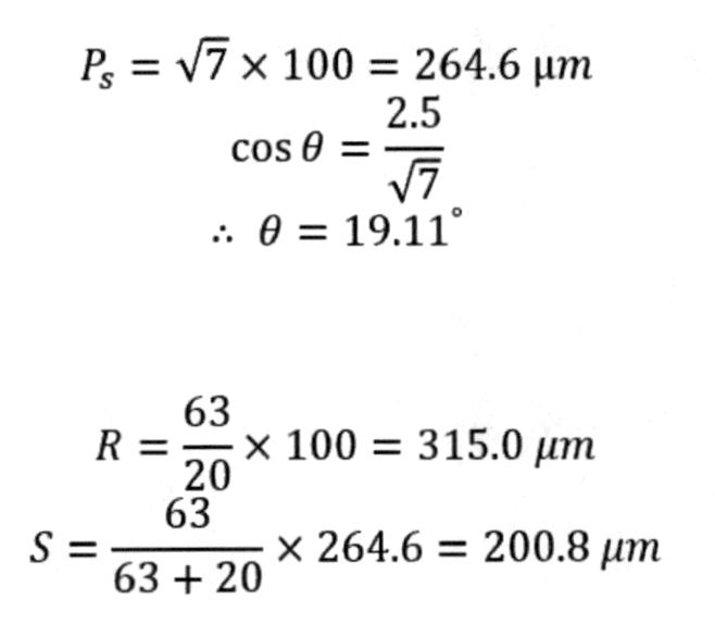
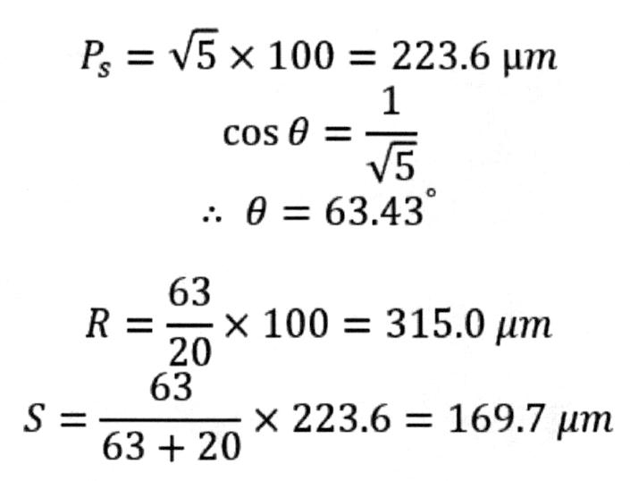
はなく、5、7、9、11、13、15等が挙げられる。奇数点の上限は、原理的には特に制限はない。照射対象Sのサイズや第2電子ビームB2のサイズ等を考慮し適宜設定すればよい。
(1)第2の実施形態と比較して、第3の実施形態では、射出配置およびレンズ配置の形状を特定し、更に、Z方向に見た射出配置を基準とした時のレンズ配置の回転角度を特定している。したがって、第2の実施形態と比較して、像面ISに形成される第2電子ビームB2の隙間をより小さくできる。
(2)走査型の電子線適用装置に適用した場合、形成した第2電子ビームB2を、重複や欠損が発生することなく、照射対象S上で走査できる。
次に、マルチ電子ビームの形成方法の第2の実施形態について説明する。マルチ電子ビームの形成方法の第2の実施形態は、電子発生源2からマルチレンズアレイ4の方向をZ方向と規定し、電子発生源2から第1電子ビームB1が射出する際の射出位置を第1電子ビーム射出位置と規定した時に、Z方向に見た時の第1電子ビーム射出位置およびマルチレンズアレイが具備するレンズの位置関係が、予め設定した位置関係となるように制御される点で、上記(マルチ電子ビームの形成方法の実施形態(以下、「方法の第1の実施形態」と記載することがある。))と異なり、その他の点は方法の第1の実施形態と同じである。したがって、マルチ電子ビームの形成方法の第2の実施形態では、方法の第1の実施形態と異なる点を中心に説明し、方法の第1の実施形態において説明済みの事項についての繰り返しとなる説明は省略する。よって、マルチ電子ビームの形成方法の第2の実施形態において明示的に説明されなかったとしても、方法の第1の実施形態で説明済みの事項を採用可能であることは言うまでもない。
Claims (15)
- 放出可能な電子を生成する電子発生源と、
前記電子発生源との間で電界を形成することができ、形成した電界により前記放出可能な電子を引き出し、電子ビームを形成するアノードと、
マルチレンズアレイと、
を含む、電子銃であって、
前記マルチレンズアレイに照射される電子ビームを第1電子ビームと規定した時に、前記第1電子ビームはm個(mは2以上の任意の整数)形成され、
前記マルチレンズアレイはn個(nは2以上の任意の整数)のレンズを具備し、
前記マルチレンズアレイから射出する電子ビームを第2電子ビームと規定した時に、前記マルチレンズアレイが具備する個々のレンズには異なる位置から照射された前記第1電子ビームが入射することで、前記第2電子ビームを最大m×n個形成できる
電子銃。 - 前記電子発生源が、フォトカソードである
請求項1に記載の電子銃。 - 前記電子発生源が、フィールドエミッタまたはショットキーである
請求項1に記載の電子銃。 - 前記電子発生源が、熱陰極である
請求項1に記載の電子銃。 - 制御部を更に含み、該制御部は、
前記電子発生源から前記マルチレンズアレイの方向をZ方向と規定し、前記m個の第1電子ビームが射出する際の射出位置を第1電子ビーム射出位置と規定した時に、
前記Z方向に見た時の前記第1電子ビーム射出位置および前記マルチレンズアレイが具備するレンズの位置関係が、予め設定した位置関係となるように制御できる
請求項1~4の何れか一項に記載の電子銃。 - 前記Z方向を回転軸として、前記マルチレンズアレイを回転する回転機構を更に含み、
前記制御部が、前記回転機構を制御する
請求項5に記載の電子銃。 - 前記Z方向を移動方向に、前記マルチレンズアレイを移動する移動機構を更に含み、
前記制御部が、前記移動機構を制御する
請求項5に記載の電子銃。 - 前記第1電子ビーム射出位置の配置を射出配置と規定し、前記マルチレンズアレイが具備するレンズの配置をレンズ配置と規定した時に、
前記射出配置および前記レンズ配置は、同一または相似した配置であり、
前記Z方向に見た前記射出配置を基準とした時に、前記Z方向に見た前記レンズ配置が、前記射出配置と同一または相似した配置とならないように、前記射出配置の中心を回転軸として回転した位置に配置される
請求項5に記載の電子銃。 - 前記射出配置および前記レンズ配置が、
直線状の等間隔の3以上の奇数点、
正方形の4隅と中心、および、
正六角形の6隅と中心、
からなる群から選択した何れか一つである
請求項8に記載の電子銃。 - 請求項1~4のいずれか一項に記載の電子銃を含む電子線適用装置であって、
電子線適用装置は、
自由電子レーザー加速器、
電子顕微鏡、
電子線ホログラフィー装置、
電子線描画装置、
電子線回折装置、
電子線検査装置、
電子線金属積層造形装置、
電子線リソグラフィー装置、
電子線加工装置、
電子線硬化装置、
電子線滅菌装置、
電子線殺菌装置、
プラズマ発生装置、
原子状元素発生装置、
スピン偏極電子線発生装置、
カソードルミネッセンス装置、または、
逆光電子分光装置
である
電子線適用装置。 - マルチ電子ビームの形成方法であって、該形成方法は、
第1電子ビーム形成工程と、
第2電子ビーム形成工程と、
を含み、
前記第1電子ビーム形成工程は、
放出可能な電子を生成する電子発生源およびアノードとの間で電界を形成することで、電子発生源からm個(mは2以上の任意の整数)の第1電子ビームを射出、または、
放出可能な電子を生成する電子発生源およびアノードとの間で電界を形成することで電子ビームを引き出し、引き出した電子ビームを分割することでm個(mは2以上の任意の整数)の第1電子ビームを形成し、
前記第2電子ビーム形成工程は、
前記m個の第1電子ビームを、n個(nは2以上の任意の整数)のレンズを具備したマルチレンズアレイに照射し、前記マルチレンズアレイが具備する個々のレンズには異なる位置から照射された前記第1電子ビームが入射することで、最大m×n個の第2電子ビームを形成する
マルチ電子ビームの形成方法。 - 前記電子発生源が、フォトカソード、フィールドエミッタ、および、ショットキーからなる群から選択した何れか一つである
請求項11に記載のマルチ電子ビームの形成方法。 - 前記電子発生源が、熱陰極であり、
前記第1電子ビーム形成工程が、
放出可能な電子を生成する電子発生源およびアノードとの間で電界を形成することで電子ビームを引き出し、引き出した電子ビームを分割することでm個(mは2以上の任意の整数)の第1電子ビームを形成する
請求項11に記載のマルチ電子ビームの形成方法。 - 前記電子発生源から前記マルチレンズアレイの方向をZ方向と規定し、前記電子発生源から前記第1電子ビームが射出する際の射出位置を第1電子ビーム射出位置と規定した時に、
前記Z方向に見た時の前記第1電子ビーム射出位置および前記マルチレンズアレイが具備するレンズの位置関係が、予め設定した位置関係となるように制御される
請求項11~13の何れか一項に記載のマルチ電子ビームの形成方法。 - 前記第1電子ビーム射出位置の配置を射出配置と規定し、前記マルチレンズアレイが具備するレンズの配置をレンズ配置と規定した時に、
前記射出配置および前記レンズ配置は、同一または相似した配置であり、
前記Z方向に見た前記射出配置を基準とした時に、前記Z方向に見た前記レンズ配置が、前記射出配置と同一または相似した配置とならないように、前記射出配置の中心を回転軸として回転した位置に配置される
請求項14に記載のマルチ電子ビームの形成方法。
Priority Applications (3)
| Application Number | Priority Date | Filing Date | Title |
|---|---|---|---|
| EP22892632.5A EP4432328A4 (en) | 2021-11-09 | 2022-10-28 | Electron gun, electron beam application device and multi-electron beam formation method |
| KR1020247018949A KR20240096776A (ko) | 2021-11-09 | 2022-10-28 | 전자총, 전자선 적용 장치 및 멀티 전자빔의 형성 방법 |
| US18/708,197 US20250343024A1 (en) | 2021-11-09 | 2022-10-28 | Electron gun, electron beam application device, and method for forming multi-electron beam |
Applications Claiming Priority (4)
| Application Number | Priority Date | Filing Date | Title |
|---|---|---|---|
| JP2021182797A JP7080533B1 (ja) | 2021-11-09 | 2021-11-09 | 電子銃、電子線適用装置およびマルチ電子ビームの形成方法 |
| JP2021-182797 | 2021-11-09 | ||
| JP2022058504A JP7105022B1 (ja) | 2022-03-31 | 2022-03-31 | 電子銃、電子線適用装置およびマルチ電子ビームの形成方法 |
| JP2022-058504 | 2022-03-31 |
Publications (1)
| Publication Number | Publication Date |
|---|---|
| WO2023085133A1 true WO2023085133A1 (ja) | 2023-05-19 |
Family
ID=86335690
Family Applications (1)
| Application Number | Title | Priority Date | Filing Date |
|---|---|---|---|
| PCT/JP2022/040542 Ceased WO2023085133A1 (ja) | 2021-11-09 | 2022-10-28 | 電子銃、電子線適用装置およびマルチ電子ビームの形成方法 |
Country Status (5)
| Country | Link |
|---|---|
| US (1) | US20250343024A1 (ja) |
| EP (1) | EP4432328A4 (ja) |
| KR (1) | KR20240096776A (ja) |
| TW (1) | TW202326786A (ja) |
| WO (1) | WO2023085133A1 (ja) |
Citations (9)
| Publication number | Priority date | Publication date | Assignee | Title |
|---|---|---|---|---|
| JPH09245708A (ja) | 1996-03-04 | 1997-09-19 | Canon Inc | 電子ビーム露光装置とその露光方法 |
| JP3537779B2 (ja) | 2001-04-13 | 2004-06-14 | 住友重機械工業株式会社 | フォトカソードの製作方法 |
| JP2013030567A (ja) | 2011-07-27 | 2013-02-07 | Canon Inc | 荷電粒子線レンズアレイ |
| JP2013544031A (ja) * | 2010-11-13 | 2013-12-09 | マッパー・リソグラフィー・アイピー・ビー.ブイ. | 中間チャンバを備えた荷電粒子リソグラフィシステム |
| JP2014053408A (ja) | 2012-09-06 | 2014-03-20 | Canon Inc | 荷電粒子線レンズ及びその製造方法 |
| JP5808021B2 (ja) | 2013-07-16 | 2015-11-10 | 国立大学法人名古屋大学 | 電子親和力の低下処理装置に用いられる活性化容器及びキット、該キットを含む電子親和力の低下処理装置、フォトカソード電子ビーム源、並びに、フォトカソード電子ビーム源を含む電子銃、自由電子レーザー加速器、透過型電子顕微鏡、走査型電子顕微鏡、電子線ホログラフィー顕微鏡、電子線描画装置、電子線回折装置及び電子線検査装置 |
| JP2016522572A (ja) * | 2013-05-03 | 2016-07-28 | マッパー・リソグラフィー・アイピー・ビー.ブイ. | ビームグリッドレイアウト |
| JP2017108146A (ja) * | 2011-04-27 | 2017-06-15 | マッパー・リソグラフィー・アイピー・ビー.ブイ. | 一つ以上の荷電粒子ビームのマニピュレーションのためのマニピュレーターデバイスを備えている荷電粒子システム |
| US20200126751A1 (en) * | 2018-10-19 | 2020-04-23 | ICT Integrated Circuit Testing Gesellschaft für Halbleiterprüftechnik mbH | Charged particle beam device, field curvature corrector, and methods of operating a charged particle beam device |
Family Cites Families (4)
| Publication number | Priority date | Publication date | Assignee | Title |
|---|---|---|---|---|
| US7274029B2 (en) * | 2004-12-28 | 2007-09-25 | Asml Netherlands B.V. | Lithographic apparatus and device manufacturing method |
| TW201133534A (en) * | 2009-09-18 | 2011-10-01 | Mapper Lithography Ip Bv | Multiple beam charged particle optical system |
| US9966230B1 (en) * | 2016-10-13 | 2018-05-08 | Kla-Tencor Corporation | Multi-column electron beam lithography including field emitters on a silicon substrate with boron layer |
| CN112119480A (zh) * | 2018-05-17 | 2020-12-22 | 日商光电魂股份有限公司 | 搭载光电阴极的电子枪的入射轴对齐方法、计算机程序以及搭载光电阴极的电子枪 |
-
2022
- 2022-10-28 EP EP22892632.5A patent/EP4432328A4/en active Pending
- 2022-10-28 KR KR1020247018949A patent/KR20240096776A/ko active Pending
- 2022-10-28 WO PCT/JP2022/040542 patent/WO2023085133A1/ja not_active Ceased
- 2022-10-28 US US18/708,197 patent/US20250343024A1/en active Pending
- 2022-11-04 TW TW111142196A patent/TW202326786A/zh unknown
Patent Citations (9)
| Publication number | Priority date | Publication date | Assignee | Title |
|---|---|---|---|---|
| JPH09245708A (ja) | 1996-03-04 | 1997-09-19 | Canon Inc | 電子ビーム露光装置とその露光方法 |
| JP3537779B2 (ja) | 2001-04-13 | 2004-06-14 | 住友重機械工業株式会社 | フォトカソードの製作方法 |
| JP2013544031A (ja) * | 2010-11-13 | 2013-12-09 | マッパー・リソグラフィー・アイピー・ビー.ブイ. | 中間チャンバを備えた荷電粒子リソグラフィシステム |
| JP2017108146A (ja) * | 2011-04-27 | 2017-06-15 | マッパー・リソグラフィー・アイピー・ビー.ブイ. | 一つ以上の荷電粒子ビームのマニピュレーションのためのマニピュレーターデバイスを備えている荷電粒子システム |
| JP2013030567A (ja) | 2011-07-27 | 2013-02-07 | Canon Inc | 荷電粒子線レンズアレイ |
| JP2014053408A (ja) | 2012-09-06 | 2014-03-20 | Canon Inc | 荷電粒子線レンズ及びその製造方法 |
| JP2016522572A (ja) * | 2013-05-03 | 2016-07-28 | マッパー・リソグラフィー・アイピー・ビー.ブイ. | ビームグリッドレイアウト |
| JP5808021B2 (ja) | 2013-07-16 | 2015-11-10 | 国立大学法人名古屋大学 | 電子親和力の低下処理装置に用いられる活性化容器及びキット、該キットを含む電子親和力の低下処理装置、フォトカソード電子ビーム源、並びに、フォトカソード電子ビーム源を含む電子銃、自由電子レーザー加速器、透過型電子顕微鏡、走査型電子顕微鏡、電子線ホログラフィー顕微鏡、電子線描画装置、電子線回折装置及び電子線検査装置 |
| US20200126751A1 (en) * | 2018-10-19 | 2020-04-23 | ICT Integrated Circuit Testing Gesellschaft für Halbleiterprüftechnik mbH | Charged particle beam device, field curvature corrector, and methods of operating a charged particle beam device |
Non-Patent Citations (1)
| Title |
|---|
| See also references of EP4432328A4 |
Also Published As
| Publication number | Publication date |
|---|---|
| TW202326786A (zh) | 2023-07-01 |
| EP4432328A4 (en) | 2025-11-05 |
| US20250343024A1 (en) | 2025-11-06 |
| KR20240096776A (ko) | 2024-06-26 |
| EP4432328A1 (en) | 2024-09-18 |
Similar Documents
| Publication | Publication Date | Title |
|---|---|---|
| US10879031B2 (en) | Apparatus of plural charged-particle beams | |
| JP6724145B2 (ja) | 複数の荷電粒子ビームの装置 | |
| CN1708826A (zh) | 电子束曝光系统 | |
| US8610082B2 (en) | Drawing apparatus and method of manufacturing article | |
| US10854424B2 (en) | Multi-electron beam device | |
| TWI768180B (zh) | 光電陰極系統、晶圓檢驗方法及晶圓檢驗工具 | |
| CN111937112A (zh) | 电子枪、电子射线应用装置、使用电子枪的电子束射出方法以及电子束的焦点位置调整方法 | |
| KR20250021298A (ko) | 광음극막으로의 다중 전자 빔 생성 | |
| JP7080533B1 (ja) | 電子銃、電子線適用装置およびマルチ電子ビームの形成方法 | |
| JP7105022B1 (ja) | 電子銃、電子線適用装置およびマルチ電子ビームの形成方法 | |
| WO2022230488A1 (ja) | 電子銃、電子線適用装置および照射位置移動方法 | |
| WO2023085133A1 (ja) | 電子銃、電子線適用装置およびマルチ電子ビームの形成方法 | |
| US12080507B2 (en) | Electron gun, electron beam applicator, emission axis verification method for electron beam emitted from photocathode, and emission axis alignment method for electron beam emitted from photocathode | |
| JP2005127800A (ja) | 電子線照射装置と照射方法および電子線描画装置 | |
| US20240212967A1 (en) | Electron gun, electron beam applicator, and emission method of electron beam | |
| KR102803626B1 (ko) | 멀티 전자 빔 묘화 장치 및 멀티 전자 빔 묘화 방법 | |
| TW202329185A (zh) | 電子射線應用裝置及電子射線應用裝置中的檢測資料之作成方法 | |
| WO2021234800A1 (ja) | 透過電子顕微鏡 | |
| TW202228178A (zh) | 電子槍、電子槍用元件、電子射線應用裝置及對位方法 | |
| CN121416392A (zh) | 一种多电子束扫描装置及成像系统 | |
| CN119890011A (zh) | 光阴极电子源、装置、产生电子的方法和电子束系统 | |
| KR20200037763A (ko) | 엑스선 영상 장치 및 그의 구동 방법 | |
| JP2007141689A (ja) | 荷電粒子ビーム照射装置 |
Legal Events
| Date | Code | Title | Description |
|---|---|---|---|
| 121 | Ep: the epo has been informed by wipo that ep was designated in this application |
Ref document number: 22892632 Country of ref document: EP Kind code of ref document: A1 |
|
| WWE | Wipo information: entry into national phase |
Ref document number: 1020247018949 Country of ref document: KR |
|
| WWE | Wipo information: entry into national phase |
Ref document number: 2022892632 Country of ref document: EP |
|
| ENP | Entry into the national phase |
Ref document number: 2022892632 Country of ref document: EP Effective date: 20240610 |
|
| WWP | Wipo information: published in national office |
Ref document number: 18708197 Country of ref document: US |