WO2023085414A1 - 多環芳香族炭化水素系光硬化性樹脂組成物 - Google Patents
多環芳香族炭化水素系光硬化性樹脂組成物 Download PDFInfo
- Publication number
- WO2023085414A1 WO2023085414A1 PCT/JP2022/042164 JP2022042164W WO2023085414A1 WO 2023085414 A1 WO2023085414 A1 WO 2023085414A1 JP 2022042164 W JP2022042164 W JP 2022042164W WO 2023085414 A1 WO2023085414 A1 WO 2023085414A1
- Authority
- WO
- WIPO (PCT)
- Prior art keywords
- group
- resin composition
- photocurable resin
- compounds
- film
- Prior art date
- Legal status (The legal status is an assumption and is not a legal conclusion. Google has not performed a legal analysis and makes no representation as to the accuracy of the status listed.)
- Ceased
Links
Classifications
-
- C—CHEMISTRY; METALLURGY
- C08—ORGANIC MACROMOLECULAR COMPOUNDS; THEIR PREPARATION OR CHEMICAL WORKING-UP; COMPOSITIONS BASED THEREON
- C08F—MACROMOLECULAR COMPOUNDS OBTAINED BY REACTIONS ONLY INVOLVING CARBON-TO-CARBON UNSATURATED BONDS
- C08F216/00—Copolymers of compounds having one or more unsaturated aliphatic radicals, each having only one carbon-to-carbon double bond, and at least one being terminated by an alcohol, ether, aldehydo, ketonic, acetal or ketal radical
- C08F216/02—Copolymers of compounds having one or more unsaturated aliphatic radicals, each having only one carbon-to-carbon double bond, and at least one being terminated by an alcohol, ether, aldehydo, ketonic, acetal or ketal radical by an alcohol radical
- C08F216/04—Acyclic compounds
-
- C—CHEMISTRY; METALLURGY
- C08—ORGANIC MACROMOLECULAR COMPOUNDS; THEIR PREPARATION OR CHEMICAL WORKING-UP; COMPOSITIONS BASED THEREON
- C08F—MACROMOLECULAR COMPOUNDS OBTAINED BY REACTIONS ONLY INVOLVING CARBON-TO-CARBON UNSATURATED BONDS
- C08F220/00—Copolymers of compounds having one or more unsaturated aliphatic radicals, each having only one carbon-to-carbon double bond, and only one being terminated by only one carboxyl radical or a salt, anhydride ester, amide, imide or nitrile thereof
- C08F220/02—Monocarboxylic acids having less than ten carbon atoms; Derivatives thereof
- C08F220/10—Esters
- C08F220/20—Esters of polyhydric alcohols or phenols, e.g. 2-hydroxyethyl (meth)acrylate or glycerol mono-(meth)acrylate
-
- C—CHEMISTRY; METALLURGY
- C08—ORGANIC MACROMOLECULAR COMPOUNDS; THEIR PREPARATION OR CHEMICAL WORKING-UP; COMPOSITIONS BASED THEREON
- C08F—MACROMOLECULAR COMPOUNDS OBTAINED BY REACTIONS ONLY INVOLVING CARBON-TO-CARBON UNSATURATED BONDS
- C08F2/00—Processes of polymerisation
- C08F2/46—Polymerisation initiated by wave energy or particle radiation
- C08F2/48—Polymerisation initiated by wave energy or particle radiation by ultraviolet or visible light
-
- C—CHEMISTRY; METALLURGY
- C08—ORGANIC MACROMOLECULAR COMPOUNDS; THEIR PREPARATION OR CHEMICAL WORKING-UP; COMPOSITIONS BASED THEREON
- C08F—MACROMOLECULAR COMPOUNDS OBTAINED BY REACTIONS ONLY INVOLVING CARBON-TO-CARBON UNSATURATED BONDS
- C08F212/00—Copolymers of compounds having one or more unsaturated aliphatic radicals, each having only one carbon-to-carbon double bond, and at least one being terminated by an aromatic carbocyclic ring
- C08F212/02—Monomers containing only one unsaturated aliphatic radical
- C08F212/04—Monomers containing only one unsaturated aliphatic radical containing one ring
-
- C—CHEMISTRY; METALLURGY
- C08—ORGANIC MACROMOLECULAR COMPOUNDS; THEIR PREPARATION OR CHEMICAL WORKING-UP; COMPOSITIONS BASED THEREON
- C08F—MACROMOLECULAR COMPOUNDS OBTAINED BY REACTIONS ONLY INVOLVING CARBON-TO-CARBON UNSATURATED BONDS
- C08F212/00—Copolymers of compounds having one or more unsaturated aliphatic radicals, each having only one carbon-to-carbon double bond, and at least one being terminated by an aromatic carbocyclic ring
- C08F212/02—Monomers containing only one unsaturated aliphatic radical
- C08F212/32—Monomers containing only one unsaturated aliphatic radical containing two or more rings
-
- C—CHEMISTRY; METALLURGY
- C08—ORGANIC MACROMOLECULAR COMPOUNDS; THEIR PREPARATION OR CHEMICAL WORKING-UP; COMPOSITIONS BASED THEREON
- C08F—MACROMOLECULAR COMPOUNDS OBTAINED BY REACTIONS ONLY INVOLVING CARBON-TO-CARBON UNSATURATED BONDS
- C08F220/00—Copolymers of compounds having one or more unsaturated aliphatic radicals, each having only one carbon-to-carbon double bond, and only one being terminated by only one carboxyl radical or a salt, anhydride ester, amide, imide or nitrile thereof
- C08F220/02—Monocarboxylic acids having less than ten carbon atoms; Derivatives thereof
- C08F220/10—Esters
- C08F220/12—Esters of monohydric alcohols or phenols
- C08F220/16—Esters of monohydric alcohols or phenols of phenols or of alcohols containing two or more carbon atoms
- C08F220/18—Esters of monohydric alcohols or phenols of phenols or of alcohols containing two or more carbon atoms with acrylic or methacrylic acids
-
- C—CHEMISTRY; METALLURGY
- C08—ORGANIC MACROMOLECULAR COMPOUNDS; THEIR PREPARATION OR CHEMICAL WORKING-UP; COMPOSITIONS BASED THEREON
- C08G—MACROMOLECULAR COMPOUNDS OBTAINED OTHERWISE THAN BY REACTIONS ONLY INVOLVING UNSATURATED CARBON-TO-CARBON BONDS
- C08G59/00—Polycondensates containing more than one epoxy group per molecule; Macromolecules obtained by polymerising compounds containing more than one epoxy group per molecule using curing agents or catalysts which react with the epoxy groups
- C08G59/14—Polycondensates modified by chemical after-treatment
-
- C—CHEMISTRY; METALLURGY
- C08—ORGANIC MACROMOLECULAR COMPOUNDS; THEIR PREPARATION OR CHEMICAL WORKING-UP; COMPOSITIONS BASED THEREON
- C08J—WORKING-UP; GENERAL PROCESSES OF COMPOUNDING; AFTER-TREATMENT NOT COVERED BY SUBCLASSES C08B, C08C, C08F, C08G or C08H
- C08J3/00—Processes of treating or compounding macromolecular substances
- C08J3/28—Treatment by wave energy or particle radiation
-
- G—PHYSICS
- G03—PHOTOGRAPHY; CINEMATOGRAPHY; ANALOGOUS TECHNIQUES USING WAVES OTHER THAN OPTICAL WAVES; ELECTROGRAPHY; HOLOGRAPHY
- G03F—PHOTOMECHANICAL PRODUCTION OF TEXTURED OR PATTERNED SURFACES, e.g. FOR PRINTING, FOR PROCESSING OF SEMICONDUCTOR DEVICES; MATERIALS THEREFOR; ORIGINALS THEREFOR; APPARATUS SPECIALLY ADAPTED THEREFOR
- G03F7/00—Photomechanical, e.g. photolithographic, production of textured or patterned surfaces, e.g. printing surfaces; Materials therefor, e.g. comprising photoresists; Apparatus specially adapted therefor
- G03F7/004—Photosensitive materials
- G03F7/038—Macromolecular compounds which are rendered insoluble or differentially wettable
-
- G—PHYSICS
- G03—PHOTOGRAPHY; CINEMATOGRAPHY; ANALOGOUS TECHNIQUES USING WAVES OTHER THAN OPTICAL WAVES; ELECTROGRAPHY; HOLOGRAPHY
- G03F—PHOTOMECHANICAL PRODUCTION OF TEXTURED OR PATTERNED SURFACES, e.g. FOR PRINTING, FOR PROCESSING OF SEMICONDUCTOR DEVICES; MATERIALS THEREFOR; ORIGINALS THEREFOR; APPARATUS SPECIALLY ADAPTED THEREFOR
- G03F7/00—Photomechanical, e.g. photolithographic, production of textured or patterned surfaces, e.g. printing surfaces; Materials therefor, e.g. comprising photoresists; Apparatus specially adapted therefor
- G03F7/004—Photosensitive materials
- G03F7/09—Photosensitive materials characterised by structural details, e.g. supports, auxiliary layers
- G03F7/11—Photosensitive materials characterised by structural details, e.g. supports, auxiliary layers having cover layers or intermediate layers, e.g. subbing layers
-
- G—PHYSICS
- G03—PHOTOGRAPHY; CINEMATOGRAPHY; ANALOGOUS TECHNIQUES USING WAVES OTHER THAN OPTICAL WAVES; ELECTROGRAPHY; HOLOGRAPHY
- G03F—PHOTOMECHANICAL PRODUCTION OF TEXTURED OR PATTERNED SURFACES, e.g. FOR PRINTING, FOR PROCESSING OF SEMICONDUCTOR DEVICES; MATERIALS THEREFOR; ORIGINALS THEREFOR; APPARATUS SPECIALLY ADAPTED THEREFOR
- G03F7/00—Photomechanical, e.g. photolithographic, production of textured or patterned surfaces, e.g. printing surfaces; Materials therefor, e.g. comprising photoresists; Apparatus specially adapted therefor
- G03F7/16—Coating processes; Apparatus therefor
- G03F7/162—Coating on a rotating support, e.g. using a whirler or a spinner
-
- H—ELECTRICITY
- H10—SEMICONDUCTOR DEVICES; ELECTRIC SOLID-STATE DEVICES NOT OTHERWISE PROVIDED FOR
- H10P—GENERIC PROCESSES OR APPARATUS FOR THE MANUFACTURE OR TREATMENT OF DEVICES COVERED BY CLASS H10
- H10P14/00—Formation of materials, e.g. in the shape of layers or pillars
- H10P14/60—Formation of materials, e.g. in the shape of layers or pillars of insulating materials
- H10P14/63—Formation of materials, e.g. in the shape of layers or pillars of insulating materials characterised by the formation processes
- H10P14/6326—Deposition processes
- H10P14/6342—Liquid deposition, e.g. spin-coating, sol-gel techniques or spray coating
-
- H—ELECTRICITY
- H10—SEMICONDUCTOR DEVICES; ELECTRIC SOLID-STATE DEVICES NOT OTHERWISE PROVIDED FOR
- H10P—GENERIC PROCESSES OR APPARATUS FOR THE MANUFACTURE OR TREATMENT OF DEVICES COVERED BY CLASS H10
- H10P14/00—Formation of materials, e.g. in the shape of layers or pillars
- H10P14/60—Formation of materials, e.g. in the shape of layers or pillars of insulating materials
- H10P14/68—Organic materials, e.g. photoresists
- H10P14/683—Organic materials, e.g. photoresists carbon-based polymeric organic materials, e.g. polyimides, poly cyclobutene or PVC
-
- H—ELECTRICITY
- H10—SEMICONDUCTOR DEVICES; ELECTRIC SOLID-STATE DEVICES NOT OTHERWISE PROVIDED FOR
- H10P—GENERIC PROCESSES OR APPARATUS FOR THE MANUFACTURE OR TREATMENT OF DEVICES COVERED BY CLASS H10
- H10P76/00—Manufacture or treatment of masks on semiconductor bodies, e.g. by lithography or photolithography
- H10P76/20—Manufacture or treatment of masks on semiconductor bodies, e.g. by lithography or photolithography of masks comprising organic materials
-
- H—ELECTRICITY
- H10—SEMICONDUCTOR DEVICES; ELECTRIC SOLID-STATE DEVICES NOT OTHERWISE PROVIDED FOR
- H10P—GENERIC PROCESSES OR APPARATUS FOR THE MANUFACTURE OR TREATMENT OF DEVICES COVERED BY CLASS H10
- H10P76/00—Manufacture or treatment of masks on semiconductor bodies, e.g. by lithography or photolithography
- H10P76/20—Manufacture or treatment of masks on semiconductor bodies, e.g. by lithography or photolithography of masks comprising organic materials
- H10P76/204—Manufacture or treatment of masks on semiconductor bodies, e.g. by lithography or photolithography of masks comprising organic materials of organic photoresist masks
- H10P76/2041—Photolithographic processes
-
- C—CHEMISTRY; METALLURGY
- C08—ORGANIC MACROMOLECULAR COMPOUNDS; THEIR PREPARATION OR CHEMICAL WORKING-UP; COMPOSITIONS BASED THEREON
- C08J—WORKING-UP; GENERAL PROCESSES OF COMPOUNDING; AFTER-TREATMENT NOT COVERED BY SUBCLASSES C08B, C08C, C08F, C08G or C08H
- C08J2367/00—Characterised by the use of polyesters obtained by reactions forming a carboxylic ester link in the main chain; Derivatives of such polymers
- C08J2367/06—Unsaturated polyesters
- C08J2367/07—Unsaturated polyesters having terminal carbon-to-carbon unsaturated bonds
Definitions
- the present invention relates to a photocurable resin composition useful in lithography processes in semiconductor manufacturing, particularly useful for forming wafer edge protection films for semiconductor manufacturing.
- a photocured film of the composition particularly a semiconductor manufacturing wafer edge protection film, a semiconductor manufacturing wafer having the photocured film, a laminated substrate using the photocurable resin composition, and a method for manufacturing a semiconductor device Regarding.
- microfabrication by lithography using a resist composition has been performed in the manufacture of semiconductor devices.
- a thin film of a photoresist composition is formed on a semiconductor substrate such as a silicon wafer, exposed to actinic rays such as ultraviolet rays through a mask pattern on which a device pattern is drawn, and developed.
- actinic rays such as ultraviolet rays
- This is a processing method in which the substrate is etched using the obtained photoresist pattern as a protective film to form fine unevenness corresponding to the pattern on the substrate surface.
- BARC bottom anti-reflective coating
- the resist film is formed using a resist containing an inorganic metal because the resolution of the resist pattern is increased when exposure is performed using extreme ultraviolet (EUV) and it has high etching resistance. is being considered.
- EUV extreme ultraviolet
- the chemical solution supplied to the front surface of the wafer wraps around the peripheral edge portions of the peripheral edge surface and the back surface of the wafer, resulting in unintended peripheral edge portions of the peripheral edge surface and the back surface.
- metal contamination of these parts may occur because the coating film is formed up to the upper part.
- a wafer processing device such as an exposure device or an etching device or a wafer transfer mechanism
- the wafer is subsequently transferred and processed through these processing devices and transfer mechanisms.
- the wafer may also be contaminated with metals, that is, cross-contamination may occur.
- Patent Document 1 When forming a coating film on the surface of a substrate, a technique has been disclosed in which the coating film can be formed so that the peripheral end face and the back side peripheral edge portion of the substrate do not come into contact with the coating film (Patent Document 1).
- Patent Document 2 A method for manufacturing a semiconductor device in which peeling of a film from a bevel portion of a substrate is suppressed is disclosed.
- An object of the present invention is to provide a photocurable resin composition that is useful in lithography processes in semiconductor manufacturing, particularly useful for forming wafer edge protection films for semiconductor manufacturing.
- a photocured film of the composition particularly a semiconductor manufacturing wafer edge protection film, a semiconductor manufacturing wafer having the photocured film, a laminated substrate using the photocurable resin composition, and a method for manufacturing a semiconductor device to provide.
- the present invention includes the following.
- a photocurable resin composition comprising a polymer and/or compound containing a polycyclic aromatic hydrocarbon group and a solvent.
- the polymer is polyvinyl alcohol, polyacrylamide, (meth)acrylic resin, polyamic acid, polyhydroxystyrene, polyhydroxystyrene derivative, polymethacrylate and maleic anhydride each containing a polycyclic aromatic hydrocarbon group.
- [6] The photocurable resin composition according to any one of [1] to [5], for forming a wafer edge protection film for semiconductor manufacturing.
- the photocurable resin composition according to [6] which has a viscosity of 100 cps or less at 25°C.
- [8] [1] A photocured film of a coating film comprising the photocurable resin composition according to any one of [1] to [7].
- [9] A wafer edge protective film for semiconductor manufacturing, which is a photocured product of a coating film comprising the photocurable resin composition according to [6] or [7].
- the wafer edge protection film for semiconductor manufacturing according to [9] having a thickness of 1 nm to 10 ⁇ m.
- [11] The wafer edge protection film for semiconductor manufacturing according to [9] or [10], for preventing metal contamination of the edge of the wafer.
- [12] A semiconductor manufacturing wafer having the edge protective film for semiconductor manufacturing wafer according to any one of [9] to [11] on the edge of the semiconductor manufacturing wafer.
- a method for producing a laminated substrate comprising a step of applying the photocurable resin composition according to any one of [1] to [7] on a substrate, and a step of exposing the applied composition.
- a method for manufacturing a semiconductor device comprising a step of applying the photocurable resin composition according to any one of [1] to [7] on a substrate, and a step of exposing the applied composition.
- [17] (A) forming a resist film on a semiconductor substrate; (B) forming a resist pattern by irradiating the resist film with light or an electron beam and then developing; (C) a step of etching the semiconductor substrate;
- Step (X) of forming a protective film from the photocurable resin composition according to [6] or [7] including, A method of manufacturing a semiconductor device.
- [18] The method for manufacturing a semiconductor device according to [17], including step (X) before step (A). [19] The method for manufacturing a semiconductor device according to [17], including step (X) between step (A) and step (B). [20] The method for manufacturing a semiconductor device according to [17], including step (X) after step (B) or step (C). [21] The method of manufacturing a semiconductor device according to any one of [17] to [20], further comprising a step (Y) of removing a portion of the resist film on the protective film after the step (X). [22] The method of manufacturing a semiconductor device according to any one of [17] to [20], including a step (Z) of removing the protective film after the step (X).
- [23] The method of manufacturing a semiconductor device according to [21], including the step (Z) of removing the protective film after the step (Y).
- [24] The method of manufacturing a semiconductor device according to any one of [17] to [23], wherein the resist film contains a metal.
- [25] Manufacture of the semiconductor device according to any one of [17] to [24], wherein in the step (X), the protective film-forming composition according to [4] is applied, and a predetermined region is exposed and developed. Method.
- [26] The method of manufacturing a semiconductor device according to [22] or [23], wherein the step (Z) is performed by ashing or treatment with hydrofluoric acid, an organic solvent, an alkaline developer, or a cleaning solution for semiconductors.
- a method for manufacturing a wafer for semiconductor manufacturing A step of applying the protective film-forming composition according to any one of [1] to [7] to the edge of a wafer precursor to manufacture a wafer with the edge protected;
- a method of manufacturing a wafer for semiconductor manufacturing comprising:
- a photocurable resin composition that is useful in lithography processes in semiconductor manufacturing, and particularly useful for forming wafer edge protection films for semiconductor manufacturing.
- a photocured film of the composition particularly a semiconductor manufacturing wafer edge protection film, a semiconductor manufacturing wafer having the photocured film, a laminated substrate using the photocurable resin composition, and a method for manufacturing a semiconductor device can be provided.
- the photocurable resin composition according to the present invention contains a polymer and/or compound containing a polycyclic aromatic hydrocarbon group and a solvent.
- polycyclic aromatic hydrocarbons refer to hydrocarbons in which multiple aromatic rings are condensed. Examples include indene, naphthalene, azulene, anthracene, phenanthrene, naphthacene, benzo[a]anthracene, triphenylene, pyrene and chrysene.
- a polycyclic aromatic hydrocarbon group is a functional group formed by removing at least one hydrogen atom from a polycyclic aromatic hydrocarbon.
- the polycyclic aromatic hydrocarbon group may have a substituent as long as the effects of the present invention are not impaired.
- polymer containing a polycyclic aromatic hydrocarbon group is not particularly limited, for example, polyvinyl alcohol, polyacrylamide, (meth)acrylic resin, polyamic acid, polyhydroxystyrene, each containing a polycyclic aromatic hydrocarbon group, Polyhydroxystyrene derivatives, copolymers of polymethacrylate and maleic anhydride, epoxy resins, phenolic resins, novolak resins, polyimides, cellulose, cellulose derivatives, starch, chitin, chitosan, gelatin, zein, sugar skeleton polymer compounds, It can be at least one selected from the group consisting of polyamide, polyethylene terephthalate, polycarbonate, polyurethane and polysiloxane. These resins are used alone or in combination of two or more.
- (Meth)acrylic resins include acrylic copolymers containing (meth)acrylic acid ester as a main component and optionally copolymerized with other monomers.
- (Meth)acrylates include methyl (meth)acrylate, ethyl (meth)acrylate, propyl (meth)acrylate, butyl (meth)acrylate, hexyl (meth)acrylate, 2-ethylhexyl (meth)acrylate, cyclohexyl (meth)acrylate, benzyl (meth)acrylate, dimethylamino (meth)acrylate, hydroxyethyl (meth)acrylate, hydroxypropyl (meth)acrylate, glycidyl (meth)acrylate.
- monomers include acrylamide, methacrylamide, acrylonitrile, methacrylonitrile, styrene, ⁇ -methylstyrene, vinyl acetate, and alkyl vinyl ether.
- carboxyl group-containing acrylic resin that has a (meth)acrylic acid ester as a main component and is copolymerized with an ethylenically unsaturated carboxylic acid and, if necessary, other monomers.
- acrylic acid, methacrylic acid, crotonic acid, maleic acid, fumaric acid, itaconic acid, and their acid anhydrides and half esters are used.
- acrylic acid, methacrylic acid, and maleic acid are preferred.
- the acrylic copolymer has a weight average molecular weight of 1,000 to 100,000, preferably 2,000 to 30,000 in terms of developability and adhesion. These can be combined as needed, and can be used singly or in combination of two or more.
- novolak resins examples include those obtained by condensing a phenol compound and an aldehyde compound or a ketone compound in the presence of an acid catalyst.
- Phenolic compounds include phenol, m-cresol, p-cresol, o-cresol, m-ethylphenol, p-ethylphenol, o-ethylphenol, 2,3,5-trimethylphenol, 2,3,5-triethyl Phenol, 4-tert-butylphenol, 3-tert-butylphenol, 2-tert-butylphenol, 2-tert-butyl-4-methylphenol, 2-tert-butyl-5-methylphenol, p-methoxyphenol, m-methoxy Phenol, p-ethoxyphenol, m-ethoxyphenol, p-propoxyphenol, m-propoxyphenol, o-isopropenylphenol, p-isopropenylphenol, 2-methyl-4-isopropenylphenol, 2-ethyl-4- isopropenylphenol, 2,3-xylenol, 2,5-xylenol, 3,5-xylenol,
- Aldehyde compounds include formaldehyde, paraformaldehyde, acetaldehyde, trioxane, propionaldehyde, butyraldehyde, trimethylacetaldehyde, acrolein, crotonaldehyde, cyclohexanealdehyde, furfural, furyl acrolein, benzaldehyde, terephthalaldehyde, phenylacetaldehyde, ⁇ -phenylpropylaldehyde, ⁇ -phenylpropylaldehyde, o-hydroxybenzaldehyde, m-hydroxybenzaldehyde, p-hydroxybenzaldehyde, o-methylbenzaldehyde, m-methylbenzaldehyde, p-methylbenzaldehyde, o-chlorobenzaldehyde, m-chlorobenzaldehyde, p-chloro
- Ketone compounds include acetone, methyl ethyl ketone, diethyl ketone, diphenyl ketone, and the like. These ketone compounds can be used alone or in combination of two or more.
- the acid catalyst used during the condensation reaction includes hydrochloric acid, sulfuric acid, formic acid, oxalic acid, p-toluenesulfonic acid and the like.
- the weight average molecular weight of the novolak resin is 1,000 to 100,000, preferably 2,000 to 30,000 in terms of developability and adhesion. These can be combined as needed, and may be used singly or in combination of two or more.
- Polyhydroxystyrene and polyhydroxystyrene derivatives include homopolymers of vinylphenol and copolymers obtained by copolymerizing vinylphenol and other compounds.
- Other compounds in this case include acrylic acid derivatives, acrylonitrile, methacrylic acid derivatives, methacrylonitrile, styrene, ⁇ -methylstyrene, p-methylstyrene, o-methylstyrene, p-methoxystyrene, p-chlorostyrene, and the like.
- Styrene derivatives are mentioned.
- polyhydroxystyrene and polyhydroxystyrene derivatives have a weight average molecular weight of 1,000 to 100,000, preferably 2,000 to 30,000 in terms of developability and adhesion. These can be combined as needed, and can be used singly or in combination of two or more.
- a preferred example of the polymer of the present invention is a polymer having a polycyclic aromatic hydrocarbon group on its side chain.
- examples thereof include (meth)acrylic resins in which the polycyclic aromatic hydrocarbon group is bonded to the main chain of the polymer via an ester bond.
- Specific examples of polymeric backbones include benzyl methacrylate, 2-naphthyl methacrylate and anthracene methyl methacrylate.
- a polymer obtained by reacting a polycyclic aromatic hydrocarbon having a carboxy group with a polymer having an epoxy group in a side chain is preferred.
- examples of polymers having epoxy groups in side chains include glycidyl methacrylate and epoxy cresol novolak.
- the compound containing a polycyclic aromatic hydrocarbon group is not particularly limited, for example, a polycyclic aromatic hydrocarbon compound having a functional group reactive with an epoxy group and the following formula (1): (In Formula (1), G represents an organic group containing an aliphatic ring, an aromatic ring, or a heterocyclic ring).
- Functional groups reactive with epoxy groups include hydroxy, acyl, acetyl, formyl, benzoyl, carboxy, carbonyl, amino, imino, cyano, azo, azide, and thiol groups. groups, sulfo groups, allyl groups and acid anhydrides, preferably carboxy groups.
- the lower limit of the weight average molecular weight of the reaction product (a) is, for example, 500, 1,000, 2,000, or 3,000, and the upper limit of the weight average molecular weight of the reaction product is, for example, 30,000, 20, 000 or 10,000.
- G in the formula (1) is a heterocyclic ring. It is preferred that the heterocycle is a triazine. Preferably, said heterocycle is 1,2,3-triazine. Preferably, said heterocyclic ring is a triazinetrione.
- the polycyclic aromatic hydrocarbon compound having a functional group reactive with an epoxy group may be a compound represented by the following formula (1-1) described in WO 2020/071361. .
- X is a divalent organic group
- A is a polycyclic aromatic hydrocarbon group
- R 1 is a halogen atom, optionally substituted carbon atoms of 1 to 40 or an optionally substituted alkoxy group having 1 to 40 carbon atoms
- n1 is an integer of 1 to 12
- n2 is an integer of 0 to 11.
- the carboxy group of formula (1-1) is a hydroxy group, an acyl group, an acetyl group, a formyl group, a benzoyl group, a carboxy group, a carbonyl group, an amino group, an imino group, a cyano group, an azo group, an azide group, a thiol group, It may be substituted with a sulfo group and an allyl group.
- polycyclic aromatic hydrocarbon compound having a functional group reactive with an epoxy group is a compound represented by the following formula (2-1) described in WO 2020/071361, good too.
- X is a divalent organic group
- A is a polycyclic aromatic hydrocarbon group
- R 2 and R 3 are each independently a hydrogen atom, an optionally substituted carbon It is an alkyl group having 1 to 10 atoms, an aryl group having 6 to 40 carbon atoms which may be substituted, or a halogen atom
- n3 is an integer of 1 to 12.
- the carboxy group of formula (2-1) is a hydroxy group, an acyl group, an acetyl group, a formyl group, a benzoyl group, a carboxy group, a carbonyl group, an amino group, an imino group, a cyano group, an azo group, an azide group, a thiol group, It may be substituted with a sulfo group and an allyl group.
- X is an ester bond, an ether bond, an amide bond, a urethane bond, or a urea bond.
- a above examples include groups derived from naphthalene, anthracene, phenanthrene, or pyrene.
- the above halogen atoms include a fluorine atom, a chlorine atom, a bromine atom and an iodine atom.
- alkyl groups include methyl, ethyl, propyl, butyl, hexyl, and pentyl groups.
- alkoxy groups include methoxy, ethoxy, propoxy, butoxy, hexoxy, and pentoxy groups.
- aryl group examples include a phenyl group and a naphthyl group.
- the "may be substituted” means that some or all of the hydrogen atoms in the alkyl group or alkoxy group may be substituted with, for example, a fluoro group or a hydroxy group.
- solvents contained in the photocurable resin composition according to the present invention include water, ethylene glycol monomethyl ether, ethylene glycol monoethyl ether, methyl cellosolve acetate, ethyl cellosolve acetate, diethylene glycol monomethyl ether, diethylene glycol monoethyl ether, and propylene.
- Glycol propylene glycol monomethyl ether, propylene glycol monoethyl ether, propylene glycol monomethyl ether acetate, propylene glycol propyl ether acetate, toluene, xylene, methyl ethyl ketone, methyl isobutyl ketone, cyclopentanone, cyclohexanone, cycloheptanone, 4-methyl-2 -pentanol, methyl 2-hydroxyisobutyrate, ethyl 2-hydroxyisobutyrate, ethyl ethoxyacetate, 2-hydroxyethyl acetate, methyl 3-methoxypropionate, ethyl 3-methoxypropionate, ethyl 3-ethoxypropionate, 3 -methyl ethoxypropionate, methyl pyruvate, ethyl pyruvate, ethyl acetate, butyl acetate, ethyl lac
- propylene glycol monomethyl ether propylene glycol monomethyl ether acetate, ethyl lactate, butyl lactate, and cyclohexanone are preferred.
- Propylene glycol monomethyl ether and propylene glycol monomethyl ether acetate are particularly preferred.
- the solvent should be added so that the photocurable resin composition according to the present invention has an appropriate viscosity. In general, it is preferably about 100 to 3,000 parts by mass with respect to 100 parts by mass of a polymer or compound containing a polycyclic aromatic hydrocarbon group.
- the polymer and/or compound containing a polycyclic aromatic hydrocarbon group according to the present invention is a crosslinked structure capable of forming a crosslinked structure by the action of light, electron beams, other electromagnetic waves, radicals, acids, heat, water, oxygen, or the like.
- polycyclic aromatic hydrocarbons e.g., epoxy groups, acrylic groups, vinyl groups, carboxylic acid groups, thiol groups, silanol groups, cinnamoyl groups, hydroxyl groups (including phenolic hydroxyl groups), etc.
- Photocuring due to radicals can occur.
- the photocurable resin composition according to the present invention can be photocured without adding any special additives.
- acid catalyst
- thermal acid generator photoacid generator
- base catalyst
- thermal base generator thermal base generator
- photobase generator antioxidant
- polymerization inhibitor polymerization inhibitor
- cross-linking agent polyfunctional acrylic, etc.
- adhesion Improving agents adhesion aids (silane coupling agents)
- surfactants defoaming agents
- rheology modifiers pigments, dyes, storage stabilizers
- dissolution accelerators such as polyhydric phenols and polyhydric carboxylic acids, sensitizers etc.
- Any radical polymerization initiator may be used as long as it can release a substance that initiates radical polymerization upon exposure to light and/or heat.
- photoradical polymerization initiators include benzophenone derivatives, imidazole derivatives, bisimidazole derivatives, N-arylglycine derivatives, organic azide compounds, titanocene compounds, aluminate complexes, organic peroxides, N-alkoxypyridinium salts, thioxanthone derivatives. etc.
- benzophenone 1,3-di(tert-butyldioxycarbonyl)benzophenone, 3,3′,4,4′-tetrakis(tert-butyldioxycarbonyl)benzophenone, 3-phenyl-5- isoxazolone, 2-mercaptobenzimidazole, bis(2,4,5-triphenyl)imidazole, 2,2-dimethoxy-1,2-diphenylethan-1-one, 1-hydroxycyclohexylphenyl ketone, 2-benzyl- 2-dimethylamino-1-(4-morpholinophenyl)-butan-1-one, bis( ⁇ 5 -2,4-cyclopentadien-1-yl)-bis(2,6-difluoro-3-(1H -pyrrol-1-yl)-phenyl)titanium) and the like, but are not limited thereto.
- radical photopolymerization initiator examples include IRGACURE (registered trademark) 651, 184, 369, 784 manufactured by BASF.
- commercial products other than the above can also be used.
- thermal radical polymerization initiators include acetyl peroxide, benzoyl peroxide, methyl ethyl ketone peroxide, cyclohexanone peroxide, hydrogen peroxide, tert-butyl hydroperoxide, cumene hydroperoxide, di-tert-butyl peroxide, dicumyl peroxide, di Peroxides such as lauroyl peroxide, tert-butylperoxyacetate, tert-butylperoxypivalate, tert-butylperoxy-2-ethylhexanoate; 2,2'-azobisisobutyronitrile, 2,2' -azobis(2,4-dimethylvaleronitrile), (1-phenylethyl)azodiphenylmethane, 2,2'-azobis(4-methoxy-2,4-dimethylvaleronitrile), dimethyl-2,2'-azobis isobutyrate, 2,2′-azo
- thermal radical polymerization initiators examples include NOF Corporation Perloyl (registered trademark) IB, NPP, IPP, SBP, TCP, OPP, SA, 355, L, Perbutyl (registered trademark) ND, NHP, MA, PV, 355, A, C, D, E, L, I, O, P, Z, Perhexyl (registered trademark) ND, PV, D, I, O, Z, Perocta (registered trademark) ND, Nyper ( Registered trademarks) PMB, BMT, BW, Pertetra (registered trademark) A, Perhexa (registered trademark) MC, TMH, HC, 250, 25B, C, 25Z, 22, V, Perocta (registered trademark) O, Percumyl (registered trademark) ) ND, D, Permenta (registered trademark) H, Nofmar (registered trademark) BC; Wako Pure Chemical Industries, Ltd.
- radical polymerization initiator Only one type of radical polymerization initiator may be used, or two or more types may be used in combination.
- the content of the radical polymerization initiator is preferably 1 part by mass or more, 2 parts by mass or more, 3 parts by mass or more and 50 parts by mass or less with respect to 100 parts by mass of the polymer and/or compound containing a ring aromatic hydrocarbon group. , 20 parts by mass or less, and 10 parts by mass or less.
- acidic compounds As the catalyst, acidic compounds, basic compounds, or various compounds that generate acid or base by heat or light can be used.
- a sulfonic acid compound or a carboxylic acid compound can be used as the acidic compound.
- An amine compound or an ammonium hydroxide compound can be used as the basic compound, and urea can be used as the compound that generates a base by heat.
- amine compounds include triethanolamine, tributanolamine, trimethylamine, triethylamine, tri-n-propylamine, tri-isopropylamine, tri-n-butylamine, tri-tert-butylamine, tri-n-octylamine, triisopropanolamine, phenyldiethanolamine, stearyl Tertiary amines such as diethanolamine and diazabicyclooctane, aromatic amines such as pyridine and 4-dimethylaminopyridine.
- Amine compounds also include primary amines such as benzylamine and n-butylamine, and secondary amines such as diethylamine and di-n-butylamine.
- ammonium hydroxide compounds include tetramethylammonium hydroxide, tetraethylammonium hydroxide, tetrapropylammonium hydroxide, tetrabutylammonium hydroxide, benzyltrimethylammonium hydroxide, benzyltriethylammonium hydroxide, cetyltrimethylammonium hydroxide, phenyltrimethylammonium hydroxide and phenyltriethylammonium hydroxide.
- thermal acid generators and photoacid generators can be used as acid generators.
- Thermal acid generators include, for example, p-toluenesulfonic acid, trifluoromethanesulfonic acid, pyridinium-p-toluenesulfonate (pyridinium-p-toluenesulfonic acid), pyridinium-p-hydroxybenzenesulfonic acid (p-phenolsulfonic acid pyridinium salt), pyridinium-trifluoromethanesulfonic acid, salicylic acid, camphorsulfonic acid, 5-sulfosalicylic acid, 4-chlorobenzenesulfonic acid, 4-hydroxybenzenesulfonic acid, benzenedisulfonic acid, 1-naphthalenesulfonic acid, citric acid, benzoic acid and sulfonic acid compounds such as hydroxybenzoic acid and carboxylic acid compounds.
- K-PURE registered trademark
- CXC-1612, CXC-1614, TAG-2172, TAG-2179, TAG-2678, and TAG2689 manufactured by King Industries
- SI-45, SI-60, SI-80, SI-100, SI-110, SI-150 manufactured by Sanshin Chemical Industry Co., Ltd.
- photoacid generators include sulfonium salts, iodonium salts, sulfonyldiazomethanes, N-sulfonyloxyimides, benzoinsulfonate-type photoacid generators, pyrogallol trisulfonate-type photoacid generators, sulfone-type photoacid generators, and glyoxime derivative-type photoacid generators. generators, oxime-O-sulfonate type acid generators, bisoxime sulfonate type acid generators and the like.
- Examples include bis(4-tert-butylphenyl)iodonium trifluoromethanesulfonate, triphenylsulfonium trifluoromethanesulfonate, phenyl-bis(trichloromethyl)-s-triazine, benzoin tosylate, and N-hydroxysuccinimide trifluoromethanesulfonate. be able to.
- the content of the photoacid generator is preferably 1 to 100 parts by weight with respect to 100 parts by weight of the polymer and/or compound containing a ring aromatic hydrocarbon group.
- thermal base generators include carbamates such as 1-methyl-1-(4-biphenylyl)ethylcarbamate and 2-cyano-1,1-dimethylethylcarbamate; urea, N,N-dimethyl-N'- ureas such as methylurea; guanidines such as guanidine trichloroacetate, guanidine phenylsulfonylacetate and guanidine phenylpropiolate; dihydropyridines such as 1,4-dihydronicotinamide; N-(isopropoxycarbonyl)-2,6-dimethyl Dimethylpiperidines such as piperidine, N-(tert-butoxycarbonyl)-2,6-dimethylpiperidine, N-(benzyloxycarbonyl)-2,6-dimethylpiperidine; tetramethylammonium phenylsulfonylacetate, tetramethylphenylpropiolate quatern
- photobase generators can be used alone or in combination of two or more types, like the photoacid generators.
- the content thereof is preferably 1 to 100 parts by weight with respect to 100 parts by weight of the polymer and/or compound containing a ring aromatic hydrocarbon group.
- a hindered phenol compound may be used, specifically 2,6-diisobutylphenol, 3,5-di-t-butylphenol, 3,5-di-t-butylcresol, hydroquinone. , hydroquinone monomethyl ether, N-nitroso-N-phenylhydroxylamine aluminum, pyrogallol, t-butylcatechol, 4-methoxy-1-naphthol, 2,6-di-t-butyl-4-methylphenol, 2,5- Di-t-butyl-hydroquinone, Octadecyl-3-(3,5-di-t-butyl-4-hydroxyphenyl)propionate, Isooctyl-3-(3,5-di-t-butyl-4-hydroxy phenyl)propionate, 4,4'-methylenebis(2,6-di-t-butylphenol), 4,4'-thio-bis(3-methyl-6-t-buty
- 1,3,5-tris(4-t-butyl-3-hydroxy-2,6-dimethylbenzyl)-1,3,5-triazine-2,4,6-(1H, 3H,5H)-trione is preferred.
- a commercial product may be used as the polymerization inhibitor, and a specific example thereof is Irganox-3114 (manufactured by BASF Japan Ltd.).
- the content of the polymerization inhibitor is preferably 0.01 to 1 part by mass, more preferably 0.01 to 0.5 parts by mass, with respect to 100 parts by mass of the polymer and/or compound containing a ring aromatic hydrocarbon group. .
- surfactants include polyoxyethylene alkyl ether compounds such as polyoxyethylene lauryl ether, polyoxyethylene stearyl ether and polyoxyethylene oleyl ether, and polyoxyethylene compounds such as polyoxyethylene octylphenol ether and polyoxyethylene nonylphenol ether.
- the content of the surfactant is preferably 0.1 parts by mass or more, 0.5 parts by mass or more, and 5 parts by mass or less with respect to 100 parts by mass of the polymer and/or compound containing a ring aromatic hydrocarbon group. Part by mass or less.
- an adhesion promoter can be included for the purpose of improving the adhesion to the substrate after development.
- adhesion promoters include chlorosilanes such as trimethylchlorosilane, dimethylvinylchlorosilane, methyldiphenylchlorosilane, chloromethyldimethylchlorosilane, trimethylmethoxysilane, dimethyldiethoxysilane, methyldimethoxysilane, and dimethylvinylethoxysilane.
- the amount of these adhesion promoters is usually 20 parts by weight or less, preferably 0.05 to 10 parts by weight, particularly preferably 0.05 to 10 parts by weight, per 100 parts by weight of the polymer and/or compound containing a ring aromatic hydrocarbon group. is 1 to 10 parts by weight.
- Dyes include acid dyes, oil-soluble dyes, disperse dyes, reactive dyes, and direct dyes.
- azo dyes benzoquinone dyes, naphthoquinone dyes, anthraquinone dyes, cyanine dyes, squarylium dyes, croconium dyes, merocyanine dyes, stilbene dyes, diphenylmethane dyes, triphenylmethane dyes, fluoran dyes dyes, spiropyran-based dyes, phthalocyanine-based dyes, indigo-based dyes, fulgide-based dyes, nickel complex-based dyes, and azulene-based dyes.
- Solvent Green 1 3, 4, 5, 7, 28, 29, 32, 33, 34, 35, C.I. I. Solvent Brown 1, 3, 4, 5, 12, 20, 22, 28, 38, 41, 42, 43, 44, 52, 53, 59, 60, 61, 62, 63, C.I. I. Solvent Black 3, 5, 5:2, 7, 13, 22, 22:1, 26, 27, 28, 29, 34, 35, 43, 45, 46, 48, 49, 50, C.I. I. Acid Red 6, 11, 26, 60, 88, 111, 186, 215, C.I. I. Acid Green 25, 27, C.I. I. Acid Blue 22, 25, 40, 78, 92, 113, 129, 167, 230, C.I. I.
- Azoic Coupling Component 2 3, 4, 5, 7, 8, 9, 10, 11, 13, 32, 37, 41, 48, C.I. I. Reactive Red 8, 22, 46, 120, C.I. I. Reactive Blue 1, 2, 7, 19, C.I. I. Reactive Violet 2, 4, C.I. I. Reactive Yellow 1, 2, 4, 14, 16, C.I. I. Reactive Orange 1, 4, 7, 13, 16, 20, C.I. I. Disperse Red 4, 11, 54, 55, 58, 65, 73, 127, 129, 141, 196, 210, 229, 354, 356, C.I. I. Disperse Blue 3, 24, 79, 82, 87, 106, 125, 165, 183, C.I. I.
- These dyes can be used singly or in combination of two or more in order to develop a desired spectral spectrum.
- the blending amount of the dye is usually selected in the range of 1 to 90% by mass with respect to the total solid content (100%) of the photocurable resin composition according to the present invention.
- the photocurable resin composition of the present application may contain a compatibilizer that suppresses deposition of the dye.
- compatibilizers that suppress the deposition of dyes include polyoxyethylene octyl ether compounds, polyoxyethylene lauryl ether compounds, polyoxyethylene alkyl (12 to 13 carbon atoms) ether compounds, polyoxyethylene secondary alkyl ( 12 to 14 carbon atoms) ether compounds, polyoxyethylene alkyl (13 carbon atoms) ether compounds, polyoxyethylene cetyl ether compounds, polyoxyethylene stearyl ether compounds, polyoxyethylene oleyl ether compounds, polyoxyethylene decyl ether compounds, poly Oxyalkylene alkyl (11 to 15 carbon atoms) ether compounds, polyoxyalkylene secondary alkyl (12 to 14 carbon atoms) ether compounds, alkyl ether compounds such as polyoxyalkylene cetyl ether compounds, polyoxyethylene lauryl amino ether compounds, poly Oxyethylene stearyl amino ether compounds, alkyl amino ether
- Sulfonic acid type compounds sulfated oleic oil compounds, castor sulfated compounds, octyl sulfate compounds, lauryl sulfate compounds, alkyl sulfate compounds, sulfate ester compounds such as alkyl ether sulfate compounds, cellulose, cellulose derivatives, and sugar skeleton polymer compounds. mentioned.
- the proportion of these compatibilizers used is usually 0.001 to 20 parts by weight per 100 parts by weight of the polymer and/or compound containing a ring aromatic hydrocarbon group. However, 20 parts by weight or more of the compatibilizing agent may be used if it does not interfere with the pattern shape.
- cross-linking agents examples include hexamethoxymethylmelamine, tetramethoxymethylbenzoguanamine, 1,3,4,6-tetrakis(methoxymethyl)glycoluril (tetramethoxymethylglycoluril) (POWDERLINK (registered trademark) 1174), 1, 3,4,6-tetrakis(butoxymethyl)glycoluril, 1,3,4,6-tetrakis(hydroxymethyl)glycoluril, 1,3-bis(hydroxymethyl)urea, 1,1,3,3-tetrakis (Butoxymethyl)urea and 1,1,3,3-tetrakis(methoxymethyl)urea.
- the cross-linking agent is a nitrogen-containing compound having 2 to 6 substituents in one molecule represented by the following formula (1d) that binds to a nitrogen atom, as described in WO 2017/187969. good too.
- R 1 represents a methyl group or an ethyl group.
- the nitrogen-containing compound having 2 to 6 substituents represented by the formula (1d) in one molecule may be a glycoluril derivative represented by the following formula (1E).
- R 1s each independently represent a methyl group or an ethyl group
- R 2 and R 3 each independently represent a hydrogen atom, an alkyl group having 1 to 4 carbon atoms, or a phenyl group.
- glycoluril derivative represented by the formula (1E) examples include compounds represented by the following formulas (1E-1) to (1E-6).
- the nitrogen-containing compound having 2 to 6 substituents represented by the formula (1d) in one molecule has 2 to 6 substituents in the molecule represented by the following formula (2d) bonded to the nitrogen atom. It can be obtained by reacting a nitrogen-containing compound with at least one compound represented by the following formula (3d).
- R 1 represents a methyl group or an ethyl group
- R 4 represents an alkyl group having 1 to 4 carbon atoms.
- the glycoluril derivative represented by the formula (1E) is obtained by reacting a glycoluril derivative represented by the following formula (2E) with at least one compound represented by the formula (3d).
- a nitrogen-containing compound having 2 to 6 substituents represented by the above formula (2d) in one molecule is, for example, a glycoluril derivative represented by the following formula (2E).
- R 2 and R 3 each independently represent a hydrogen atom, an alkyl group having 1 to 4 carbon atoms, or a phenyl group, and R 4 each independently represent an alkyl group having 1 to 4 carbon atoms. represents.
- glycoluril derivative represented by the formula (2E) examples include compounds represented by the following formulas (2E-1) to (2E-4). Furthermore, examples of the compound represented by the formula (3d) include compounds represented by the following formulas (3d-1) and (3d-2).
- crosslinkable compounds can be used alone or in combination of two or more.
- a cross-linking agent When a cross-linking agent is used, its content is generally 1% to 50% by mass, preferably 5% to 30% by mass, based on the reaction product. Also, the content thereof is preferably 1 to 200 parts by weight with respect to 100 parts by weight of the polymer and/or compound containing a ring aromatic hydrocarbon group.
- the photocurable resin composition according to the present invention has at least one partial structure selected from partial structures (I) represented by the following formulas (1-1) to (1-7) described in WO2018/190380 can further include a compound comprising :
- R 1 , R 1a , R 3 , R 5a and R 6a are each independently an alkylene group having 1 to 10 carbon atoms, an arylene group having 6 to 40 carbon atoms (the alkylene group and the arylene group optionally substituted with one or more amido or amino groups), an oxygen atom, a carbonyl group, a sulfur atom, —C(O)—NR a —, —NR b —, or Represents a divalent group consisting of a combination of
- Each R 5 is independently a nitrogen atom, or a nitrogen atom and an alkylene group having 1 to 10 carbon atoms, or an arylene group having 6 to 40 carbon atoms (the alkylene group and arylene group are one or more at least one selected from the group consisting of an oxygen atom, a carbonyl group, a sulfur atom, —C(O)—NR a — and —NR b —
- the photocurable resin composition according to the present invention may further contain polysiloxane.
- the polysiloxane may be a modified polysiloxane in which some of the silanol groups are modified, for example, a modified polysiloxane in which some of the silanol groups are alcohol-modified or acetal-protected.
- Polysiloxane may be, for example, a hydrolytic condensate of a hydrolyzable silane, or a modified product in which at least part of the silanol groups of the hydrolytic condensate is alcohol-modified or acetal-protected (hereinafter referred to as It may be referred to as a “modified product of hydrolytic condensate”.).
- the hydrolyzable silane associated with the hydrolytic condensate can contain one or more hydrolyzable silanes.
- the polysiloxane can have any structure having a cage-type, ladder-type, straight-chain, or branched main chain. Furthermore, commercially available polysiloxanes can be used.
- the "hydrolytic condensate" of the hydrolyzable silane that is, the product of hydrolytic condensation, includes not only the polyorganosiloxane polymer, which is a condensate in which the condensation has been completely completed, but also Also included are polyorganosiloxane polymers that are incomplete partial hydrolytic condensates.
- Such a partially hydrolyzed condensate is also a polymer obtained by hydrolysis and condensation of a hydrolyzable silane, similar to the condensate in which the condensation is completely completed, but it stops at partial hydrolysis and condenses. , and therefore the Si--OH groups remain.
- polysiloxanes examples include hydrolytic condensates of hydrolyzable silanes containing at least one hydrolyzable silane represented by the following formula (11) or modified products thereof.
- R 1 is a group bonded to a silicon atom and independently of each other, an optionally substituted alkyl group, an optionally substituted aryl group, an optionally substituted aralkyl optionally substituted halogenated alkyl group, optionally substituted halogenated aryl group, optionally substituted halogenated aralkyl group, optionally substituted alkoxyalkyl group, optionally substituted an alkoxyaryl group, an optionally substituted alkoxyaralkyl group, or an optionally substituted alkenyl group, or an organic group having an epoxy group, an organic group having an acryloyl group, or an organic group having a methacryloyl group; It represents an organic group having a mercapto group, an organic group having an amino group, an organic group having an alkoxy group, an organic group having a sulfonyl group, an organic group having a cyano group, or a combination of two or more thereof.
- R 2 is a
- each group and atom in R 1 in formula (11) and preferred carbon numbers thereof include the groups and carbon numbers described above for R 3 in formulas (A-1) and (A-2). can be mentioned.
- Specific examples of each group and atom for R 2 in formula (11) and their preferred number of carbon atoms include the groups and atoms described above for X in formulas (A-1) and (A-2), and carbon I can name a few.
- hydrolyzable silanes represented by formula (11) include tetramethoxysilane, tetrachlorosilane, tetraacetoxysilane, tetraethoxysilane, tetra-n-propoxysilane, tetra-i-propoxysilane, tetra-n -butoxysilane, methyltrimethoxysilane, methyltrichlorosilane, methyltriacetoxysilane, methyltriethoxysilane, methyltripropoxysilane, methyltributoxysilane, methyltriamyloxysilane, methyltriphenoxysilane, methyltribenzyloxysilane, methyltriphenethyloxysilane, glycidoxymethyltrimethoxysilane, glycidoxymethyltriethoxysilane, ⁇ -glycidoxyethyltrimethoxysilane, ⁇ -glycidoxye
- the photocurable resin composition according to the present invention is described in JP-A-2016-003160, (A) a polyfunctional epoxy (meth)acrylate compound, (B) a polyfunctional thiol compound and (C) a radical polymerization initiator may be further contained.
- the component (A) may have a molecular weight of 300 to 20,000.
- the component (A) may be a bisphenol-type polyfunctional epoxy (meth)acrylate compound.
- the component (B) may be liquid at 25°C.
- (D) a polymerization inhibitor may be contained.
- the photocurable resin composition according to the present invention may be a film-forming composition further comprising a photopolymerizable substance and a photoinitiator, as described in WO2009/104643.
- the photopolymerizable substance may be a compound having at least one cationic polymerizable reactive group, and the cationic polymerization initiator may be a photocationic polymerization initiator.
- the photopolymerizable substance may be a compound having at least one radically polymerizable reactive group, and the photopolymerization initiator may be a radical photopolymerization initiator.
- the photopolymerizable compound may be a sugar compound.
- the sugar compounds may be monosaccharide or disaccharide compounds.
- the sugar compound has the formula (10):
- G 1 represents a sugar skeleton
- T represents a divalent linking group
- R 1 represents a vinyl group or glycidyl group
- R 2 represents a hydrogen atom or a hydroxyl group
- n and L are 0 or 1, respectively.
- p is an integer representing the total number of hydroxyl groups possessed by the sugar
- m is an integer satisfying 1 ⁇ m ⁇ (pm).
- the photopolymerizable compound may be an alicyclic epoxy compound or an alicyclic oxetane compound.
- the alicyclic epoxy compound may be a cycloalkylene oxide derivative.
- the alicyclic epoxy compound is represented by formula (2) or formula (3):
- G2 represents a monovalent to pentavalent linking group having an alkylene group, carbonyloxy group, heterocyclic ring, aromatic ring, or a combination thereof
- G3 represents an alkyl group, an alkylcarbonyl group, a heterocyclic ring, an aromatic an organic group having a ring or a combination thereof
- n and m each represent an integer of 1 to 5
- the method for preparing the photocurable resin composition of the present application is not particularly limited. That is, a polymer and/or compound containing a polycyclic aromatic hydrocarbon group, a solvent, and other components may be mixed in an arbitrary ratio and in an arbitrary order to form a uniform solution.
- the photocurable resin composition in a solution state thus prepared is preferably used after being filtered using a filter or the like having a pore size of about 0.2 ⁇ m.
- the solid content that is, the concentration range of the components excluding the solvent can be appropriately selected depending on the application. For example, it is usually 5 to 50% by mass, preferably 10 to 30% by mass, for forming a resist underlayer film, and usually 0.01% by mass to 0.01% by mass for forming a wafer edge protection film for semiconductor manufacturing. 10% by mass.
- the photocurable resin composition according to the present invention is coated on a semiconductor substrate, and the coated composition is baked to produce a resist underlayer film, which can be used to produce a semiconductor device.
- Semiconductor substrates to which the photocurable resin composition according to the present invention is applied include, for example, silicon wafers, germanium wafers, and compound semiconductor wafers such as gallium arsenide, indium phosphide, gallium nitride, indium nitride, and aluminum nitride. mentioned.
- the inorganic film is formed by, for example, an ALD (atomic layer deposition) method, a CVD (chemical vapor deposition) method, a reactive sputtering method, an ion plating method, or a vacuum deposition method. It is formed by a spin coating method (spin on glass: SOG).
- the inorganic film examples include a polysilicon film, a silicon oxide film, a silicon nitride film, a BPSG (Boro-Phospho Silicate Glass) film, a titanium nitride film, a titanium oxynitride film, a tungsten film, a gallium nitride film, and a gallium arsenide film. is mentioned.
- the photocurable resin composition according to the present invention is applied onto such a semiconductor substrate by an appropriate coating method such as spinner or coater. Thereafter, a resist underlayer film is formed by baking using a heating means such as a hot plate. Baking conditions are appropriately selected from a baking temperature of 100° C. to 400° C. and a baking time of 0.3 minutes to 60 minutes. Preferably, the baking temperature is 120° C. to 350° C. and the baking time is 0.5 minutes to 30 minutes, and more preferably the baking temperature is 150° C. to 300° C. and the baking time is 0.8 minutes to 10 minutes.
- the film thickness of the resist underlayer film to be formed is, for example, 0.001 ⁇ m (1 nm) to 10 ⁇ m, 0.002 ⁇ m (2 nm) to 1 ⁇ m, 0.005 ⁇ m (5 nm) to 0.5 ⁇ m (500 nm), 0.001 ⁇ m (1 nm).
- the manufacturing method of the patterned substrate goes through the following steps. Usually, it is manufactured by forming a photoresist layer on a resist underlayer film.
- the photoresist formed by coating and baking on the resist underlayer film by a method known per se is not particularly limited as long as it is sensitive to the light used for exposure. Both negative and positive photoresists can be used.
- positive photoresist composed of novolac resin and 1,2-naphthoquinonediazide sulfonic acid ester;
- a chemically amplified photoresist comprising a low-molecular compound that decomposes to increase the alkali dissolution rate of the photoresist, an alkali-soluble binder, and a photoacid generator, and a binder having a group that decomposes with an acid to increase the alkali dissolution rate.
- Examples thereof include V146G (trade name) manufactured by JSR Corporation, APEX-E (trade name) manufactured by Shipley, PAR710 (trade name) manufactured by Sumitomo Chemical Co., Ltd., and AR2772 and SEPR430 (trade name) manufactured by Shin-Etsu Chemical Co., Ltd.. Also, for example, Proc. SPIE, Vol. 3999, 330-334 (2000), Proc. SPIE, Vol. 3999, 357-364 (2000), and Proc. SPIE, Vol. 3999, 365-374 (2000).
- resist compositions include the following compositions.
- Actinic ray-sensitive or sensitive resin containing a resin A having a repeating unit having an acid-decomposable group in which the polar group is protected by a protective group that is released by the action of an acid, and a compound represented by the general formula (21) A radioactive resin composition.
- m represents an integer of 1-6.
- R 1 and R 2 each independently represent a fluorine atom or a perfluoroalkyl group.
- L 1 represents -O-, -S-, -COO-, -SO 2 -, or -SO 3 -.
- L2 represents an optionally substituted alkylene group or a single bond.
- W1 represents an optionally substituted cyclic organic group.
- M + represents a cation.
- a radiation-sensitive resin comprising a polymer having a first structural unit represented by the following formula (31) and a second structural unit represented by the following formula (32) containing an acid-labile group, and an acid generator. Composition.
- Ar is a group obtained by removing (n+1) hydrogen atoms from arene having 6 to 20 carbon atoms.
- R 1 is a hydroxy group, a sulfanyl group, or a monovalent group having 1 to 20 carbon atoms.
- n is an integer of 0 to 11.
- R 2 is a hydrogen atom, a fluorine atom, a methyl group or a trifluoromethyl group.
- R 3 is a monovalent group having 1 to 20 carbon atoms containing the acid dissociable group
- Z is a single bond, an oxygen atom or a sulfur atom
- R 4 is , a hydrogen atom, a fluorine atom, a methyl group or a trifluoromethyl group.
- R 2 represents an alkyl group having 1 to 6 carbon atoms which may have a halogen atom, a hydrogen atom or a halogen atom
- X 1 is a single bond
- -CO-O-* or -CO-NR 4 -* * represents a bond with -Ar
- R 4 represents a hydrogen atom or an alkyl group having 1 to 4 carbon atoms
- Ar is one or more groups selected from the group consisting of a hydroxy group and a carboxyl group represents an aromatic hydrocarbon group having 6 to 20 carbon atoms which may have ]
- resist films examples include the following.
- R A is each independently a hydrogen atom or a methyl group
- R 1 and R 2 are each independently a tertiary alkyl group having 4 to 6 carbon atoms
- Each R 3 is independently a fluorine atom or a methyl group
- m is an integer of 0 to 4
- X 1 is a single bond, a phenylene group or a naphthylene group, an ester bond, a lactone ring, or a phenylene is a linking group having 1 to 12 carbon atoms and containing at least one selected from a group and a naphthylene group
- X 2 is a single bond, an ester bond or an amide bond.
- resist materials include the following.
- R A is a hydrogen atom or a methyl group.
- X 1 is a single bond or an ester group.
- X 2 is a linear, branched or cyclic carbon an alkylene group having 1 to 12 carbon atoms or an arylene group having 6 to 10 carbon atoms, and part of the methylene groups constituting the alkylene group may be substituted with an ether group, an ester group or a lactone ring-containing group,
- at least one hydrogen atom contained in X 2 is substituted with a bromine atom
- X 3 is a single bond, an ether group, an ester group, or a linear, branched or cyclic group having 1 to 12 carbon atoms.
- Rf 1 to Rf 4 independently represents a hydrogen atom, a fluorine atom or a trifluoro a methyl group, at least one of which is a fluorine atom or a trifluoromethyl group, and Rf 1 and Rf 2 may combine to form a carbonyl group
- R 1 to R 5 each independently linear, branched or cyclic alkyl groups having 1 to 12 carbon atoms, linear, branched or cyclic alkenyl groups having 2 to 12 carbon atoms, alkynyl groups having 2 to 12 carbon atoms, and 6 to 20 carbon atoms an aryl group, an aralkyl group having 7 to 12 carbon atoms, or an aryloxyalkyl group having 7 to 12 carbon atoms, and some or all of the hydrogen atoms of these groups are hydroxy groups, carboxy groups,
- R A is a hydrogen atom or a methyl group.
- R 1 is a hydrogen atom or an acid labile group.
- R 2 is a linear, branched or cyclic C 1 to 6 alkyl groups or halogen atoms other than bromine,
- X 1 is a single bond or a phenylene group, or a linear, branched or cyclic C 1-12 group which may contain an ester group or a lactone ring is an alkylene group of X 2 is -O-, -O-CH 2 - or -NH-,
- m is an integer of 1 to 4, and
- n is an integer of 0 to 3.
- a resist composition that generates acid upon exposure and whose solubility in a developer changes due to the action of the acid, Containing a base component (A) whose solubility in a developer changes under the action of an acid and a fluorine additive component (F) which exhibits decomposability in an alkaline developer,
- each Rf 21 is independently a hydrogen atom, an alkyl group, an alkoxy group, a hydroxyl group, a hydroxyalkyl group, or a cyano group.
- n" is an integer of 0 to 2. * is a bond.
- the structural unit (f1) includes a structural unit represented by the following general formula (f1-1) or a structural unit represented by the following general formula (f1-2).
- each R is independently a hydrogen atom, an alkyl group having 1 to 5 carbon atoms, or a halogenated alkyl group having 1 to 5 carbon atoms.
- X is a divalent linking group having no acid-labile site.
- a aryl is an optionally substituted divalent aromatic cyclic group.
- X 01 is a single bond or a divalent linking group.
- Each R 2 is independently an organic group having a fluorine atom.
- coatings examples include the following.
- An inorganic oxo/hydroxo-based composition An inorganic oxo/hydroxo-based composition.
- a coating solution comprising an organic solvent and a first organometallic compound represented by the formula RSnO (3/2-x/2) (OH) x where 0 ⁇ x ⁇ 3, wherein the solution from about 0.0025M to about 1.5M tin, and R is an alkyl or cycloalkyl group having 3 to 31 carbon atoms, wherein said alkyl or cycloalkyl group is a secondary or secondary A coating solution bonded to tin at a tertiary carbon atom.
- RSnO (3/2-x/2) (OH) x where 0 ⁇ x ⁇ 3, wherein the solution from about 0.0025M to about 1.5M tin, and R is an alkyl or cycloalkyl group having 3 to 31 carbon atoms, wherein said alkyl or cycloalkyl group is a secondary or secondary A coating solution bonded to tin at a tertiary carbon atom.
- An aqueous inorganic pattern-forming precursor comprising a mixture of water, a metal suboxide cation, a polyatomic inorganic anion, and a radiation-sensitive ligand comprising a peroxide group.
- Exposure is performed through a mask (reticle) for forming a predetermined pattern, and for example, i-ray, KrF excimer laser, ArF excimer laser, EUV (extreme ultraviolet) or EB (electron beam) is used. is preferably applied for EB (electron beam) or EUV (extreme ultraviolet) exposure, and preferably for EUV (extreme ultraviolet) exposure.
- An alkaline developer is used for development, and the development temperature is selected from 5° C. to 50° C. and the development time is appropriately selected from 10 seconds to 300 seconds.
- alkaline developer examples include inorganic alkalis such as sodium hydroxide, potassium hydroxide, sodium carbonate, sodium silicate, sodium metasilicate, aqueous ammonia, primary amines such as ethylamine and n-propylamine, diethylamine, secondary amines such as di-n-butylamine; tertiary amines such as triethylamine and methyldiethylamine; alcohol amines such as dimethylethanolamine and triethanolamine; Aqueous solutions of alkalis such as quaternary ammonium salts, pyrrole, cyclic amines such as piperidine, and the like can be used.
- inorganic alkalis such as sodium hydroxide, potassium hydroxide, sodium carbonate, sodium silicate, sodium metasilicate, aqueous ammonia, primary amines such as ethylamine and n-propylamine, diethylamine, secondary amines such as di-n-butyl
- an alcohol such as isopropyl alcohol or a nonionic surfactant may be added in an appropriate amount to the aqueous alkali solution.
- Preferred developers among these are quaternary ammonium salts, more preferably tetramethylammonium hydroxide and choline.
- a surfactant or the like can be added to these developers. It is also possible to use a method of developing with an organic solvent such as butyl acetate instead of the alkaline developer, and developing the portion where the rate of alkali dissolution of the photoresist is not improved.
- the resist underlayer film is dry-etched.
- the inorganic film is formed on the surface of the semiconductor substrate used, the surface of the inorganic film is exposed, and when the inorganic film is not formed on the surface of the semiconductor substrate used, the semiconductor substrate is exposed. expose the surface.
- the substrate is processed by a method known per se (dry etching method, etc.), and a semiconductor device can be manufactured.
- the photocurable resin composition according to the present invention can also be used to form a wafer edge protection film for semiconductor manufacturing. A case of using the photocurable resin composition according to the present invention to form a wafer edge protection film for semiconductor manufacturing will be described below.
- a method for manufacturing a semiconductor device includes: (A) forming a resist film on a semiconductor substrate; (B) forming a resist pattern by irradiating the resist film with light or an electron beam and then developing; (C) a step of etching the semiconductor substrate; In a method of manufacturing a semiconductor device comprising on the front edge and optionally the bevel and/or the back edge of a semiconductor fabrication wafer, Step (X) of forming a protective film from the photocurable resin composition according to the present invention including, A method for manufacturing a semiconductor device.
- a resist film is formed on a semiconductor substrate.
- Semiconductor substrates are wafers used for the manufacture of semiconductor devices and the like, and include commonly used silicon wafers, germanium wafers, gallium arsenide, indium phosphide, gallium nitride, indium nitride, and aluminum nitride.
- a compound semiconductor wafer formed by combining two or more kinds of elements such as They are usually disc-shaped and have sizes of, for example, 4, 6, 8, 12 inches, and the like. Commercial products may be used.
- the inorganic film is formed by, for example, an ALD (atomic layer deposition) method, a CVD (chemical vapor deposition) method, a reactive sputtering method, an ion plating method, or a vacuum deposition method. It is formed by a spin coating method (spin on glass: SOG).
- the inorganic film examples include a polysilicon film, a silicon oxide film, a silicon nitride film, a BPSG (Boro-Phospho Silicate Glass) film, a titanium nitride film, a titanium oxynitride film, a tungsten film, a gallium nitride film, and a gallium arsenide film. is mentioned.
- a resist underlayer film, a resist film, etc., having a predetermined thickness are formed on such a semiconductor substrate by an appropriate coating method such as a spray, spinner, or coater.
- an appropriate coating method such as a spray, spinner, or coater.
- each of the resist underlayer film-forming composition, the resist film-forming composition, and the like is supplied through a nozzle or the like from above the central portion of the rotating disk-shaped substrate.
- These films are typically baked using a heating means such as a hot plate.
- the photocurable resin composition according to the present invention as a composition for forming a protective film preferably has a viscosity of about 100 cps or less at 25°C. .
- a viscosity is a measured value by an E-type viscometer.
- the photoresist used for forming the resist film is not particularly limited as long as it is sensitive to the light used for exposure. Both negative and positive photoresists can be used.
- positive photoresist composed of novolac resin and 1,2-naphthoquinonediazide sulfonic acid ester;
- a chemically amplified photoresist comprising a low-molecular compound that decomposes to increase the alkali dissolution rate of the photoresist, an alkali-soluble binder, and a photoacid generator, and a binder having a group that decomposes with an acid to increase the alkali dissolution rate.
- photoresists composed of low-molecular-weight compounds and photoacid generators that are decomposed by acid to increase the rate of alkali dissolution of photoresists, and resists containing metal elements.
- Examples include V146G (trade name) manufactured by JSR Corporation, APEX-E (trade name) manufactured by Shipley, PAR710 (trade name) manufactured by Sumitomo Chemical Co., Ltd., AR2772 (trade name) and SEPR430 (trade name) manufactured by Shin-Etsu Chemical Co., Ltd., and the like.
- Proc. SPIE Vol. 3999, 330-334 (2000)
- Proc. SPIE Vol. 3999, 357-364 (2000)
- Proc. SPIE Vol. 3999, 365-374 (2000).
- a negative photoresist is preferred.
- the resist film-forming composition used for forming the resist film can contain one or more metals.
- the form of the metal include simple metals, metal salts, metal complexes, and other metal-containing compounds.
- Metal species are not particularly limited, but examples include tin, indium, antimony, bismuth, gallium, germanium, aluminum, zirconium, hafnium, cerium, lanthanum, and cesium.
- Baking conditions for the resist film are appropriately selected from a baking temperature of 70° C. to 400° C. and a baking time of 0.3 minutes to 60 minutes.
- the baking temperature is 80° C. to 350° C.
- the baking time is 0.5 minutes to 30 minutes
- the baking temperature is 90° C. to 300° C.
- the baking time is 0.8 minute to 10 minutes.
- the lower limit of the average thickness of the resist film is preferably 1 nm, more preferably 3 nm, 5 nm and 10 nm.
- the upper limit of the average thickness of the resist film is 5,000 nm, 3,000 nm, 2,000 nm, preferably 1,000 nm, more preferably 500 nm, 200 nm, still more preferably 50 nm.
- Step (X) of forming a protective film The step (X) of forming a protective film from the photocurable resin composition on the front edge and optionally the bevel and/or the back edge of the semiconductor manufacturing wafer is performed at any time.
- a photocurable resin composition is applied, and a predetermined region is exposed and developed.
- Step (X) may be performed before step (A), between step (A) and step (B), or after step (B) or step (C). good.
- the surface of the substrate on which the device portion such as the resist film is provided is called the front surface, and the opposite surface is called the back surface.
- the front surface edge refers to a region generally having a width of 1 to 10 mm from the edge of the device portion provided on the substrate to the bevel portion, and the bevel portion connects the front surface edge and the back surface edge.
- the bent area is defined as the edge of the rear surface, and the edge of the rear surface of the substrate is the area corresponding to the edge of the front surface of the rear surface of the substrate.
- the photocurable resin composition according to the present invention is applied to a semiconductor substrate on which a resist film or the like is formed.
- the method of applying the photocurable resin composition is not particularly limited, but known means such as a spin coating method (spin coating method) and a spray method can be employed.
- spin coating method spin coating method
- spray method a spray method
- the photocurable resin composition is applied above or near the edge of the surface of the rotating disk-shaped substrate. through a nozzle from Preferably, the beveled portion and/or the backside edge of the substrate are also fed through the nozzle from the vicinity of each.
- the spin coating conditions can be selected as appropriate and are not limited at all, but typical conditions are as follows.
- ⁇ Viscosity of photocurable resin composition about 100 cps or less
- ⁇ Wafer rotation speed ..
- the photocurable resin composition is exposed.
- the photocurable resin composition is exposed to actinic rays such as ultraviolet rays, visible rays, and radiation (i-ray, KrF excimer laser, ArF excimer laser, EUV (extreme ultraviolet rays), through a mask or without a mask. EB (including electron beam)) can be applied.
- soft baking SB
- post-exposure baking PEB
- the post-exposure heating temperature is preferably 50° C. to 150° C.
- the post-exposure heating time is preferably 1 to 10 minutes.
- the photocurable resin composition is cured with light having a wavelength of preferably 170 to 800 nm (more preferably 200 to 600 nm, still more preferably 300 to 500 nm).
- the photocurable resin composition after exposure is developed.
- Development can be carried out by removing the exposed portion of the photocurable resin composition after exposure with a developer, and the development temperature is appropriately selected from 5° C. to 50° C. and the development time is selected from 10 seconds to 300 seconds.
- organic solvents contained in the developer include alcohol solvents, ether solvents, ketone solvents, amide solvents, ester solvents, hydrocarbon solvents, and the like.
- organic solvent for the developer those containing an ester solvent, a ketone solvent, or a combination thereof are preferable.
- the developer may contain one type of organic solvent alone, or may contain two or more types.
- alcohol solvents examples include aliphatic monoalcohol solvents having 1 to 18 carbon atoms such as 4-methyl-2-pentanol and n-hexanol; alicyclic monoalcohols having 3 to 18 carbon atoms such as cyclohexanol. system solvent; polyhydric alcohol partial ether system solvent having 3 to 19 carbon atoms such as propylene glycol monomethyl ether.
- ether solvents include dialkyl ether solvents such as diethyl ether, dipropyl ether, dibutyl ether, dipentyl ether, diisoamyl ether, dihexyl ether, and diheptyl ether; cyclic ether solvents such as tetrahydrofuran and tetrahydropyran; and diphenyl ether. and aromatic ring-containing ether solvents such as anisole.
- dialkyl ether solvents such as diethyl ether, dipropyl ether, dibutyl ether, dipentyl ether, diisoamyl ether, dihexyl ether, and diheptyl ether
- cyclic ether solvents such as tetrahydrofuran and tetrahydropyran
- diphenyl ether diphenyl ether.
- aromatic ring-containing ether solvents such as anisole.
- Ketone solvents include, for example, acetone, methyl ethyl ketone, methyl-n-propyl ketone, methyl-n-butyl ketone, diethyl ketone, methyl-iso-butyl ketone, 2-heptanone, ethyl-n-butyl ketone, methyl-n-hexyl ketone.
- di-iso-butyl ketone, trimethylnonanone and other chain ketone solvents cyclopentanone, cyclohexanone, cycloheptanone, cyclooctanone, methylcyclohexanone and other cyclic ketone solvents: 2,4-pentanedione, acetonyl Acetone, acetophenone, and the like.
- amide solvents include cyclic amide solvents such as N,N'-dimethylimidazolidinone and N-methylpyrrolidone; N-methylformamide, N,N-dimethylformamide, N,N-diethylformamide, acetamide, Chain amide solvents such as N-methylacetamide, N,N-dimethylacetamide, N-methylpropionamide and the like are included.
- ester solvents include monocarboxylic acid ester solvents such as n-butyl acetate and ethyl lactate; polyhydric alcohol carboxylate solvents such as propylene glycol acetate; polyhydric alcohol partial ether carboxylates such as propylene glycol monomethyl ether acetate; rate-based solvents; polyvalent carboxylic acid diester-based solvents such as diethyl oxalate; and carbonate-based solvents such as dimethyl carbonate and diethyl carbonate.
- monocarboxylic acid ester solvents such as n-butyl acetate and ethyl lactate
- polyhydric alcohol carboxylate solvents such as propylene glycol acetate
- polyhydric alcohol partial ether carboxylates such as propylene glycol monomethyl ether acetate
- rate-based solvents polyvalent carboxylic acid diester-based solvents
- carbonate-based solvents such as dimethyl carbonate and diethyl carbonate.
- hydrocarbon solvents examples include aliphatic hydrocarbon solvents having 5 to 12 carbon atoms such as n-pentane and n-hexane; aromatic hydrocarbon solvents having 6 to 16 carbon atoms such as toluene and xylene. mentioned.
- ester-based solvents propylene glycol monomethyl ether acetate is preferred. Cyclohexanone is preferred as the ketone solvent. Propylene glycol monomethyl ether is preferable as the ether solvent.
- the lower limit of the content of the organic solvent in the developer is preferably 80% by mass, more preferably 90% by mass, even more preferably 99% by mass, and particularly preferably 100% by mass.
- the developer may contain a nitrogen-containing compound.
- the developer contains a nitrogen-containing compound, it is possible to further reduce film loss in the formed resist pattern.
- an aqueous developer may be used instead of the organic solvent-based developer described above.
- alkaline aqueous solutions such as sodium hydroxide, potassium hydroxide, sodium silicate, ammonia, monoethylamine, diethylamine, triethylamine, triethanolamine, and tetramethylammonium hydroxide may be used.
- the base concentration of these aqueous solutions is not particularly limited, but can be, for example, 0.1 to 10% by mass.
- alcohols and surfactants can be added to the developer and used. Each of these can be blended in the range of preferably 0.01 to 10 parts by weight, more preferably 0.1 to 5 parts by weight, per 100 parts by weight of the developer.
- surfactants include ionic and nonionic fluorine-based surfactants, silicon-based surfactants, and the like.
- Examples of the development method include a method in which the substrate is immersed in a bath filled with a developer for a certain period of time (dip method), and a method in which the developer is piled up on the surface of the substrate by surface tension and left stationary for a certain period of time (paddle method). ), a method in which the developer is sprayed onto the surface of the substrate (spray method), and a method in which the developer dispensing nozzle scans the substrate rotating at a constant speed and continuously dispenses the developer (dynamic dispensing method). etc.
- the heating temperature in the heat treatment is usually 150°C or higher and 350°C or lower, preferably 200 to 300°C.
- the heat treatment time is the time until the photocurable resin composition is cured, and is preferably less than 30 minutes in general in consideration of productivity.
- the lower limits of the average thickness of the protective film are, for example, 1 nm, 3 nm, 5 nm, 10 nm, 30 nm, 50 nm, 80 nm, 100 nm, 150 nm and 200 nm.
- the upper limits of the average thickness of the protective film are, for example, 10 ⁇ m, 8 ⁇ m, 5 ⁇ m, 3 ⁇ m, 1 ⁇ m, 800 nm, 500 nm, and 300 nm.
- the protective film that covers the edges of semiconductor manufacturing substrates has properties such as the ability to prevent metal contamination on the edges of the wafer, as well as dry etching resistance, phosphoric acid resistance, tetramethylammonium hydroxide (TMAH) resistance, HF removability, scratch resistance, good embeddability for stepped substrates, low amount of sublimation, affinity for hydrophobic substrates, no crater foreign matter left on wafer side, good edge shape, inner hump (nozzle injection hole) It is desirable to satisfy the function of suppressing the phenomenon that the film-forming composition remains in the form of nodules immediately below.
- TMAH tetramethylammonium hydroxide
- the photocurable resin composition according to the present invention is provided by applying the photosensitive photocurable resin composition (negative type) to the front surface edge portion of the substrate and optionally to the bevel portion and/or the back surface edge portion. After coating, the bevel portion can be accurately covered with the protective film by exposing and developing the portion of the film to be cured.
- Photosensitivity makes it easy to control the film thickness of the protective film on the wafer edge, remove the inner hump, improve the edge shape, and correct the deviation of the center position during spin coating. has the advantage of
- the resist film on the protective film can be removed with a remover.
- a remover Similar to the step (X), it is preferable to apply the remover to the front surface edge of the semiconductor manufacturing wafer and, optionally, the bevel portion and/or the back surface edge.
- the resist remover includes, for example, propylene glycol monomethyl ether, propylene glycol monomethyl ether acetate, cyclohexanone, water, butyl acetate, tetramethylammonium aqueous solution, or mixtures thereof.
- propylene glycol monomethyl ether acetate and water are preferable from the viewpoint of removability of the resist film.
- the protective film can be removed by ashing or treatment with hydrofluoric acid, an organic solvent, an alkaline developer, or a cleaning solution for semiconductors. After that, it is preferable to wash with an arbitrary solvent or a commonly used semiconductor cleaning liquid.
- Steps (X), (Y), and (Z) can be performed simultaneously with steps (A), (B), and (C), or at any time before or after each step.
- step (X) when step (X) is included before step (A), step (Y) of removing the resist film above the protective film may be performed between step (A) and step (B). can be performed, and the step (Z) of removing the protective film can be performed between the step (Y) and the step (B).
- step (X) is included between step (A) and step (B) or step (C)
- protection A step (Z) of removing the film can also be performed.
- Step of forming a resist pattern by irradiating a resist film with light or an electron beam and subsequent development, and (C) Step of processing a semiconductor substrate by etching The resist film is exposed through a mask (reticle) for forming a predetermined pattern, for example, i-ray, KrF excimer laser, ArF excimer laser, EUV (extreme ultraviolet) or EB (electron beam) is used. .
- a mask for forming a predetermined pattern
- i-ray, KrF excimer laser, ArF excimer laser, EUV (extreme ultraviolet) or EB (electron beam) is used.
- soft baking SB
- post-exposure baking PEB
- the post-exposure heating temperature is preferably 50° C. to 150° C.
- the post-exposure heating time is preferably 1 to 10 minutes.
- alkaline developer is used for development, and the development temperature is appropriately selected from 5°C to 50°C and the development time is 10 seconds to 300 seconds.
- alkaline developing solutions include inorganic alkalis such as sodium hydroxide, potassium hydroxide, sodium carbonate, sodium silicate, sodium metasilicate, aqueous ammonia, primary amines such as ethylamine and n-propylamine, diethylamine, secondary amines such as di-n-butylamine; tertiary amines such as triethylamine and methyldiethylamine; alcohol amines such as dimethylethanolamine and triethanolamine; Aqueous solutions of alkalis such as quaternary ammonium salts, pyrrole, cyclic amines such as piperidine, and the like can be used.
- the base concentration of these aqueous solutions is not particularly limited, but can be, for example, 0.1 to 10% by mass.
- alcohols such as isopropyl alcohol and surfactants such as nonionic surfactants can be added in appropriate amounts to the aqueous solution of alkalis.
- surfactants such as nonionic surfactants
- Each of these can be blended in the range of preferably 0.01 to 10 parts by weight, more preferably 0.1 to 5 parts by weight, per 100 parts by weight of the developer.
- Preferred developers among these are quaternary ammonium salts, more preferably tetramethylammonium hydroxide and choline.
- a surfactant or the like can be added to these developers.
- Parts where the alkali dissolution rate of the photoresist is not improved by developing with a polyhydric alcohol solvent having 2 to 18 carbon atoms such as 1,2-propylene glycol or an organic solvent such as butyl acetate instead of the alkaline developer. can also be used.
- the semiconductor substrate is baked.
- the baking means is not particularly limited, for example, a proximity baking furnace in which a plurality of substrate support pins are used to secure a gap between the substrate and the hot plate is preferably used.
- the baking temperature is usually 40° C. to 300° C., preferably 200° C. to 300° C. for 1 to 30 minutes, but may be set to 90° C. or less if it is necessary to avoid damage to the resist pattern.
- Baking may be performed on the semiconductor substrate after exposure and before development.
- the means and conditions for baking are as described above, but if it is necessary to avoid damage to the resist pattern, the temperature may be set to 90° C. or less.
- the resist underlayer film is etched, preferably dry etched, to form a patterned resist.
- the semiconductor substrate is processed by a method known per se (dry etching method, etc.) using the patterned resist.
- the etching for processing the semiconductor substrate may be a known method.
- the shape processing step is performed by dry etching using a fluorine-based gas such as carbon tetrafluoride.
- it includes a surface treatment step such as removing a silicon nitride film present on the surface of the semiconductor substrate with hot phosphoric acid.
- a semiconductor device can be manufactured through the above processes.
- the method for manufacturing a wafer for semiconductor manufacturing according to the present invention is the method for manufacturing a semiconductor device as described above, wherein the photocurable resin composition according to the present invention is added to the surface end portion of the wafer precursor for semiconductor manufacturing and optionally It includes a step of applying (or coating) the bevel portion and/or the back surface edge portion, and manufacturing a semiconductor manufacturing wafer with a protective film.
- a semiconductor manufacturing wafer precursor refers to a product obtained by subjecting a semiconductor substrate to at least one step of a semiconductor device manufacturing method.
- the step of forming an inorganic film, a resist underlayer film, a resist film, etc. on a semiconductor substrate is performed, and the resist film is irradiated with light or an electron beam, and then Examples include materials before being subjected to the step of forming a resist pattern by development of a.
- the photocurable resin composition according to the present invention is applied by spin coating.
- the semiconductor substrate may then be baked.
- the baking means is not particularly limited, but for example, a proximity baking furnace that secures a gap between the substrate and the hot plate using a plurality of substrate support pins is preferably used.
- the baking temperature is usually 40-300° C., preferably 200-300° C., for 1-30 minutes.
- the wafer for semiconductor manufacturing of the present invention is a wafer for semiconductor manufacturing in which the edge of the wafer is protected, and the photocurable resin composition containing a polymer having a crosslinkable group and a solvent is applied to the edge of the wafer. It is a formed wafer for semiconductor manufacturing.
- the weight-average molecular weights of the polymers shown in Synthesis Examples and Comparative Synthesis Examples below in this specification are the results of measurement by gel permeation chromatography (hereinafter abbreviated as GPC).
- GPC gel permeation chromatography
- composition 1 composition 1
- composition 2 composition 2
- composition 3 composition 3
- a polyethylene microfilter having a pore size of 0.10 ⁇ m was prepared. was filtered to prepare a photocurable resin composition.
- each of the photocurable resin compositions prepared in Examples 1, 2 and Comparative Example 1 was applied onto a silicon wafer using a spinner. Bake on a hot plate at 80° C. for 1 minute, and then irradiate light with a wavelength of 365 nm at an intensity of 0.3 J/cm 2 and 3 J/cm 2 using an i-line aligner (PLA-501, Canon Inc.). A photocured film (thickness: 0.10 ⁇ m) was formed. Then, the dry etching rate (nm/min) of these photocured films was measured using an etcher (RIE-10NR) manufactured by Samco under the condition of using CF 4 as a dry etching gas.
- RIE-10NR etcher manufactured by Samco under the condition of using CF 4 as a dry etching gas.
- a photocurable resin composition that is useful in lithography processes in semiconductor manufacturing, and particularly useful for forming wafer edge protection films for semiconductor manufacturing.
- a photocured film of the composition particularly a semiconductor manufacturing wafer edge protection film, a semiconductor manufacturing wafer having the photocured film, a laminated substrate using the photocurable resin composition, and a method for manufacturing a semiconductor device can be provided.
Landscapes
- Chemical & Material Sciences (AREA)
- Health & Medical Sciences (AREA)
- Chemical Kinetics & Catalysis (AREA)
- Medicinal Chemistry (AREA)
- Polymers & Plastics (AREA)
- Organic Chemistry (AREA)
- Physics & Mathematics (AREA)
- General Physics & Mathematics (AREA)
- Architecture (AREA)
- Structural Engineering (AREA)
- Engineering & Computer Science (AREA)
- General Chemical & Material Sciences (AREA)
- Spectroscopy & Molecular Physics (AREA)
- Materials For Photolithography (AREA)
- Compositions Of Macromolecular Compounds (AREA)
Abstract
Description
また、当該組成物の光硬化膜、特に半導体製造用ウエハ端部保護膜、当該光硬化膜を有する半導体製造用ウエハ、並びに光硬化性樹脂組成物を利用した積層基板、及び半導体装置の製造方法に関する。
また、当該組成物の光硬化膜、特に半導体製造用ウエハ端部保護膜、当該光硬化膜を有する半導体製造用ウエハ、並びに光硬化性樹脂組成物を利用した積層基板、及び半導体装置の製造方法提供することである。
[1]
多環芳香族炭化水素基を含有するポリマー及び/又は化合物、並びに溶剤を含む、光硬化性樹脂組成物。
[2]
前記多環芳香族炭化水素基が、ナフタレン、アントラセン、フェナントレン及びピレンからなる群より選ばれる少なくとも1種に由来する、[1]に記載の光硬化性樹脂組成物。
[3]
前記ポリマーが、それぞれ多環芳香族炭化水素基を含有するポリビニルアルコール、ポリアクリルアミド、(メタ)アクリル系樹脂、ポリアミド酸、ポリヒドロキシスチレン、ポリヒドロキシスチレン誘導体、ポリメタクリレートとマレイン酸無水物との共重合体、エポキシ樹脂、フェノール樹脂、ノボラック樹脂、ポリイミド、セルロース、セルロース誘導体、スターチ、キチン、キトサン、ゼラチン、ゼイン、糖骨格高分子化合物、ポリアミド、ポリエチレンテレフタレート、ポリカーボネート、ポリウレタン及びポリシロキサンからなる群より選ばれる少なくとも1種である、[1]に記載の光硬化性樹脂組成物。
[4]
前記化合物が、複素環構造を更に含む、[1]~[3]何れか1項に記載の光硬化性樹脂組成物。
[5]
170~800nmの波長の光で硬化する、[1]~[4]何れか1項に記載の光硬化性樹脂組成物。
[6]
半導体製造用ウエハ端部保護膜を形成するための、[1]~[5]何れか1項に記載の光硬化性樹脂組成物。
[7]
25℃において100cps以下の粘度を有する、[6]に記載の光硬化性樹脂組成物。
[8]
[1]~[7]何れか1項に記載の光硬化性樹脂組成物からなる塗布膜の光硬化膜。
[9]
[6]又は[7]に記載の光硬化性樹脂組成物からなる塗布膜の光硬化物である半導体製造用ウエハ端部保護膜。
[10]
1nm~10μmの厚みを有する、[9]に記載の半導体製造用ウエハ端部保護膜。
[11]
ウエハ端部の金属汚染を防止するための、[9]又は[10]に記載の半導体製造用ウエハ端部保護膜。
[12]
半導体製造用ウエハの端部に、[9]~[11]何れか1項に記載の半導体製造用ウエハ端部保護膜を有する、半導体製造用ウエハ。
[13]
半導体製造用ウエハ端部保護膜を形成するための、[1]~[7]何れか1項に記載の光硬化性樹脂組成物の使用。
[14]
基板上に、[1]~[7]何れか1項に記載の光硬化性樹脂組成物を塗布する工程、及び塗布された組成物を露光する工程を含む、積層基板の製造方法。
[15]
前記基板が、段差を有する、[14]に記載の積層基板の製造方法。
[16]
基板上に、[1]~[7]何れか1項に記載の光硬化性樹脂組成物を塗布する工程、及び塗布された組成物を露光する工程を含む、半導体装置の製造方法。
[17]
(A) 半導体基板上にレジスト膜を形成する工程と、
(B) レジスト膜に対する光又は電子線の照射とその後の現像によりレジストパターンを形成する工程と、
(C) 半導体基板をエッチングで加工する工程と、
を含む半導体装置の製造方法において、
半導体製造用ウエハの表面端部と、任意選択的にベベル部及び/又は裏面端部に、
[6]又は[7]に記載の光硬化性樹脂組成物からの保護膜を形成する工程(X)
を含む、
半導体装置の製造方法。
[18]
工程(A)の前に工程(X)を含む、[17]に記載の半導体装置の製造方法。
[19]
工程(A)と工程(B)との間に工程(X)を含む、[17]に記載の半導体装置の製造方法。
[20]
工程(B)又は工程(C)の後に工程(X)を含む、[17]に記載の半導体装置の製造方法。
[21]
工程(X)の後に、前記保護膜の上の部分のレジスト膜を除去する工程(Y)を含む、[17]~[20]何れか1項に記載の半導体装置の製造方法。
[22]
工程(X)の後に、前記保護膜を除去する工程(Z)を含む、[17]~[20]何れか1項に記載の半導体装置の製造方法。
[23]
工程(Y)の後に、前記保護膜を除去する工程(Z)を含む、[21]に記載の半導体装置の製造方法。
[24]
前記レジスト膜が金属を含む、[17]~[23]何れか1項に記載の半導体装置の製造方法。
[25]
前記工程(X)において、[4]に記載の保護膜形成組成物を塗布し、所定の領域に露光、現像を行う、[17]~[24]何れか1項に記載の半導体装置の製造方法。
[26]
工程(Z)をアッシング、又はフッ化水素酸、有機溶剤、アルカリ現像液、若しくは半導体用洗浄液による処理により行う、[22]又は[23]に記載の半導体装置の製造方法。
[27]
半導体製造用ウエハの製造方法であって、
ウエハ前駆体の端部に、[1]~[7]何れか1項に記載の保護膜形成用組成物を塗布し、前記端部が保護されたウエハを製造する工程、
を含む、半導体製造用ウエハの製造方法。
また、当該組成物の光硬化膜、特に半導体製造用ウエハ端部保護膜、当該光硬化膜を有する半導体製造用ウエハ、並びに光硬化性樹脂組成物を利用した積層基板、及び半導体装置の製造方法を提供することができる。
本発明に係る光硬化性樹脂組成物は、多環芳香族炭化水素基を含有するポリマー及び/又は化合物、並びに溶剤を含む。
多環芳香族炭化水素基を含有するポリマーは特に限定されないが、例えば、それぞれ多環芳香族炭化水素基を含有するポリビニルアルコール、ポリアクリルアミド、(メタ)アクリル系樹脂、ポリアミド酸、ポリヒドロキシスチレン、ポリヒドロキシスチレン誘導体、ポリメタクリレートとマレイン酸無水物との共重合体、エポキシ樹脂、フェノール樹脂、ノボラック樹脂、ポリイミド、セルロース、セルロース誘導体、スターチ、キチン、キトサン、ゼラチン、ゼイン、糖骨格高分子化合物、ポリアミド、ポリエチレンテレフタレート、ポリカーボネート、ポリウレタン及びポリシロキサンからなる群より選ばれる少なくとも1種とすることができる。これらの樹脂は、単独で、または2種類以上組み合わせて用いられる。
側鎖にエポキシ基を有するポリマーに、カルボキシ基を有する多環芳香族炭化水素を反応させて得られるポリマーが好ましい。側鎖にエポキシ基を有するポリマーとしては、グルシジルメタクリレートやエポキシクレゾールノボラックが挙げられる。
多環芳香族炭化水素基を含有する化合物は特に限定されないが、例えば、エポキシ基と反応性を有する官能基を有する多環芳香族炭化水素化合物と、下記式(1):

(式(1)中、Gは脂肪族環、芳香族環又は複素環を含む有機基を表す)で表される化合物との反応生成物が挙げられる。


(上記式(1-1)中、Xは2価の有機基であり、Aは多環芳香族炭化水素基であり、R1はハロゲン原子、置換されていてもよい炭素原子数1~40のアルキル基、又は置換されていてもよい炭素原子数1~40のアルコキシ基であり、n1は1~12の整数であり、n2は0~11の整数である。)
式(1-1)のカルボキシ基が、ヒドロキシ基、アシル基、アセチル基、ホルミル基、ベンゾイル基、カルボキシ基、カルボニル基、アミノ基、イミノ基、シアノ基、アゾ基、アジ基、チオール基、スルホ基及びアリル基に置き換わっていてもよい。
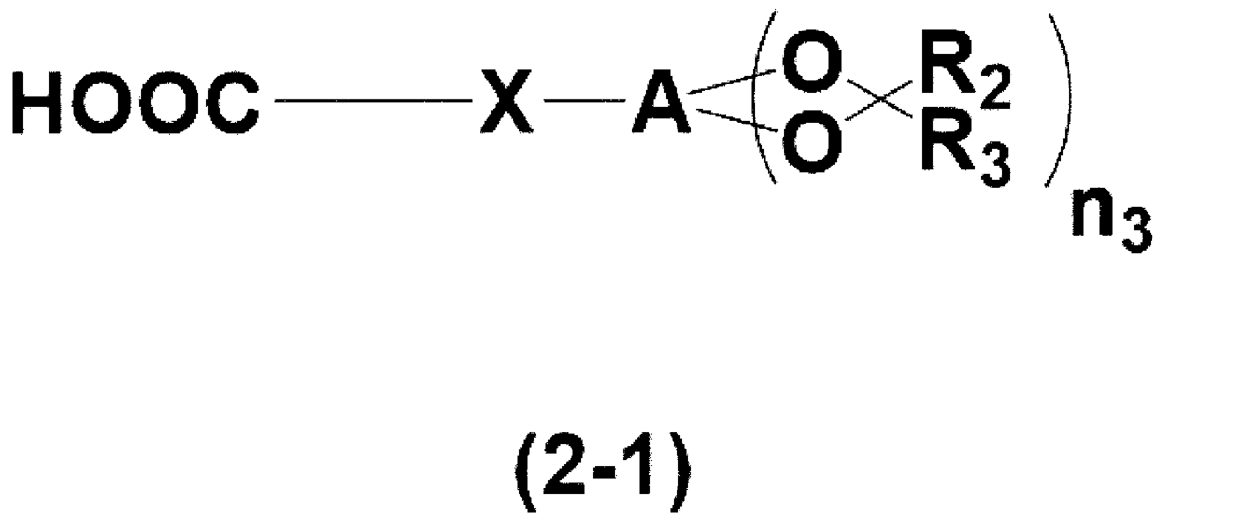
(上記式(2-1)中、Xは2価の有機基であり、Aは多環芳香族炭化水素基であり、R2及びR3は各々独立に水素原子、置換されてもよい炭素原子数1~10のアルキル基、置換されてもよい炭素原子数6~40のアリール基又はハロゲン原子であり、n3は1~12の整数である。
式(2-1)のカルボキシ基が、ヒドロキシ基、アシル基、アセチル基、ホルミル基、ベンゾイル基、カルボキシ基、カルボニル基、アミノ基、イミノ基、シアノ基、アゾ基、アジ基、チオール基、スルホ基及びアリル基に置き換わっていてもよい。
本発明に係る光硬化性樹脂組成物に含まれる溶剤としては、例えば、水、エチレングリコールモノメチルエーテル、エチレングリコールモノエチルエーテル、メチルセロソルブアセテート、エチルセロソルブアセテート、ジエチレングリコールモノメチルエーテル、ジエチレングリコールモノエチルエーテル、プロピレングリコール、プロピレングリコールモノメチルエーテル、プロピレングリコールモノエチルエーテル、プロピレングリコールモノメチルエーテルアセテート、プロピレングリコールプロピルエーテルアセテート、トルエン、キシレン、メチルエチルケトン、メチルイソブチルケトン、シクロペンタノン、シクロヘキサノン、シクロヘプタノン、4-メチル-2-ペンタノール、2-ヒドロキシイソ酪酸メチル、2-ヒドロキシイソ酪酸エチル、エトキシ酢酸エチル、酢酸2-ヒドロキシエチル、3-メトキシプロピオン酸メチル、3-メトキシプロピオン酸エチル、3-エトキシプロピオン酸エチル、3-エトキシプロピオン酸メチル、ピルビン酸メチル、ピルビン酸エチル、酢酸エチル、酢酸ブチル、乳酸エチル、乳酸ブチル、2-ヘプタノン、メトキシシクロペンタン、アニソール、γ-ブチロラクトン、N-メチルピロリドン、N,N-ジメチルホルムアミド、及びN,N-ジメチルアセトアミドが挙げられる。これらの溶剤は、単独で又は2種以上を組み合わせて用いることができる。
スルホン酸化合物又はカルボン酸化合物として、例えば、p-トルエンスルホン酸、トリフルオロメタンスルホン酸、ピリジニウムトリフルオロメタンスルホナート(=ピリジニウムトリフルオロメタンスルホン酸)、ピリジニウム-p-トルエンスルホネート、ピリジニウム-4-ヒドロキシベンゼンスルホナート、サリチル酸、カンファースルホン酸、5-スルホサリチル酸、4-クロロベンゼンスルホン酸、4-フェノールスルホン酸、ピリジニウム-4-フェノールスルホネート、ベンゼンジスルホン酸、1-ナフタレンスルホン酸、4-ニトロベンゼンスルホン酸、クエン酸、安息香酸、ヒドロキシ安息香酸が挙げられる。
アミン化合物として、例えば、トリエタノールアミン、トリブタノールアミン、トリメチルアミン、トリエチルアミン、トリノルマルプロピルアミン、トリイソプロピルアミン、トリノルマルブチルアミン、トリ-tert-ブチルアミン、トリノルマルオクチルアミン、トリイソプロパノールアミン、フェニルジエタノールアミン、ステアリルジエタノールアミン、及びジアザビシクロオクタン等の第3級アミン、ピリジン及び4-ジメチルアミノピリジン等の芳香族アミンが挙げられる。また、ベンジルアミン及びノルマルブチルアミン等の第1級アミン、ジエチルアミン及びジノルマルブチルアミン等の第2級アミンもアミン化合物として挙げられる。
水酸化アンモニウム化合物としては、例えば、水酸化テトラメチルアンモニウム、水酸化テトラエチルアンモニウム、水酸化テトラプロピルアンモニウム、水酸化テトラブチルアンモニウム、水酸化ベンジルトリメチルアンモニウム、水酸化ベンジルトリエチルアンモニウム、水酸化セチルトリメチルアンモニウム、水酸化フェニルトリメチルアンモニウム、水酸化フェニルトリエチルアンモニウムが挙げられる。
市販品としては、例えば、K-PURE〔登録商標〕CXC-1612、同CXC-1614、同TAG-2172、同TAG-2179、同TAG-2678、同TAG2689(以上、King Industries社製)、及びSI-45、SI-60、SI-80、SI-100、SI-110、SI-150(以上、三新化学工業株式会社製)が挙げられる。
ヒンダードフェノール化合物の中でも、1,3,5-トリス(4-t-ブチル-3-ヒドロキシ-2,6-ジメチルベンジル)-1,3,5-トリアジン-2,4,6-(1H,3H,5H)-トリオンが好ましい。
上記重合禁止剤は市販品を使用してもよく、具体例としてはIrganox-3114(BASFジャパン株式会社製)が挙げられる。
染料の析出を抑制する相溶化剤の具体例としては、ポリオキシエチレンオクチルエーテル化合物、ポリオキシエチレンラウリルエーテル化合物、ポリオキシエチレンアルキル(炭素数12~13)エーテル化合物、ポリオキシエチレン2級アルキル(炭素数12~14)エーテル化合物、ポリオキシエチレンアルキル(炭素数13)エーテル化合物、ポリオキシエチレンセチルエーテル化合物、ポリオキシエチレンステアリルエーテル化合物、ポリオキシエチレンオレイルエーテル化合物、ポリオキシエチレンデシルエーテル化合物、ポリオキシアルキレンアルキル(炭素数11~15)エーテル化合物、ポリオキシアルキレン2級アルキル(炭素数12~14)エーテル化合物、ポリオキシアルキレンセチルエーテル化合物等のアルキルエーテル化合物、ポリオキシエチレンラウリルアミノエーテル化合物、ポリオキシエチレンステアリルアミノエーテル化合物、ポリオキシエチレンオレイルアミノエーテル化合物等のアルキルアミノエーテル化合物、ポリオキシエチレンラウリン酸アミドエーテル化合物、ポリオキシエチレンステアリン酸アミドエーテル化合物、ポリオキシエチレンオレイン酸アミドエーテル化合物、ラウリン酸ジエタノールアミド化合物、ステアリン酸ジエタノールアミド化合物、オレイン酸ジエタノールアミド化合物等のアルキルアミドエーテル化合物、ポリオキシエチレンポリスチルフェニルエーテル化合物、ポリオキシアルキレンポリスチルフェニルエーテル化合物、ポリオキシアルキレンポリスチルフェニルエーテルホルムアミド縮合物、ポリオキシエチレンモノスチリルフェニルエーテル化合物、ポリオキシエチレンジスチリルフェニルエーテル化合物、ポリオキシエチレンナフチルエーテル化合物等のアリルフェニルエーテル化合物、グリセリンモノラウレート化合物、グリセリンモノステアレート化合物、グリセリンモノオレート化合物、グリセリントリオレート化合物等のグリセリン脂肪酸エステル化合物、ソルビタンモノラウレート化合物、ソルビタンモノパルミテート化合物、ソルビタンモノステアレート化合物、ソルビタントリステアレート化合物、ソルビタンモノオレート化合物、ソルビタントリオレート化合物等のソルビタン酸エステル化合物、ポリオキシエチレンジラウレート化合物、ポリオキシエチレンラウレート化合物、ポリオキシエチレンステアレート化合物、ポリオキシエチレンジステアレート化合物、ポリオキシエチレンジオレート化合物、ポリオキシエチレンオレート化合物等の脂肪酸エーテルエステル化合物、ポリオキシエチレンヒマシ油エーテル化合物、ポリオキシエチレン硬化ヒマシ油エーテル化合物等の植物油エーテルエステル化合物、ポリオキシエチレンソルビタンモノラウレート化合物、ポリオキシエチレンソルビタンモノステアレート化合物、ポリオキシエチレンソルビタンモノオレート化合物、ポリオキシエチレンスルビタントリオレート化合物等のソルビタンエーテルエステル化合物、ポリオキシアルキレンブチルエーテル化合物、ポリオキシアルキレンオクチルエーテル化合物、ポリオキシアルキレンアルキル(炭素数14~15)エーテル化合物、ポリオキシアルキレンオレイルエーテル化合物等のモノオール型ポリエーテル化合物、ポリオキシエチレンポリオキシプロピレン縮合物等のジオール型ポリエーテル化合物、トリメチロールプロパントリス(ポリオキシアルキレン)エーテル化合物、ポリオキシアルキレングリセリルエーテル化合物等のポリオール型ポリエーテル化合物、メチルラウレート化合物、メチルオレート化合物、イソプロピルミリステート化合物、ブチルステアレート化合物、オクチルパルミテート化合物、オクチルステアレート化合物、ラウリルオレート化合物、イソトリデシルステアレート化合物、オレイルオレート化合物、ジオレイルアジペート化合物、トリメチロールプロパントリデカノエート化合物、トリメチロールプロパントリラウレート化合物、ペンタエリスリトールジオレート化合物、ペンタエリスリトールモノステアレート化合物、ペンタエリスリトールジステアレート化合物等の脂肪酸アルキルエステル化合物、アルキルスルホネート化合物、長鎖アルキルベンゼンスルホン酸化合物、分岐アルキルベンゼンスルホン酸化合物、長鎖アルキルベンゼンスルホネート化合物、分岐アルキルベンゼンスルホネート化合物、分岐アルキルジフェニルエーテルジスルホネート化合物、モノイソプロピルナフタレンスルホネート化合物、ジイソプロピルナフタレンスルホネート化合物、トリイソプロピルナフタレンスルホネート化合物、ジブチルナフタレンスルホネート化合物、ジオクチルスルホサクシネート化合物等のスルホン酸型化合物、オレイン酸硫酸化油化合物、ヒマシ硫酸化化合物、オクチルサルフェート化合物、ラウリルサルフェート化合物、アルキルサルフェート化合物、アルキルエーテルサルフェート化合物等の硫酸エステル化合物、セルロース、セルロース誘導体、糖骨格高分子化合物が挙げられる。


(式(1E)中、4つのR1はそれぞれ独立にメチル基又はエチル基を表し、R2及びR3はそれぞれ独立に水素原子、炭素原子数1~4のアルキル基、又はフェニル基を表す。)
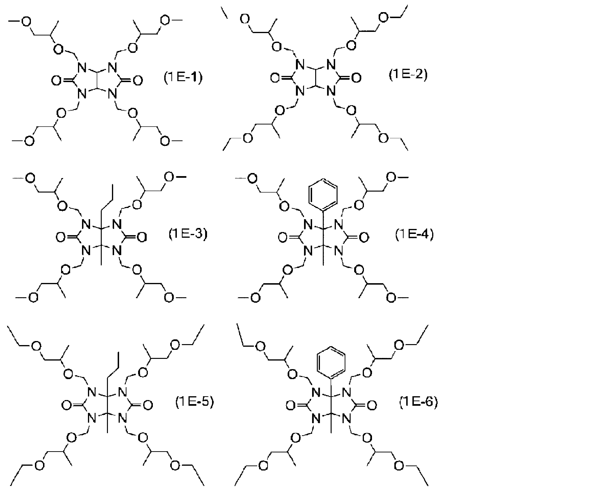
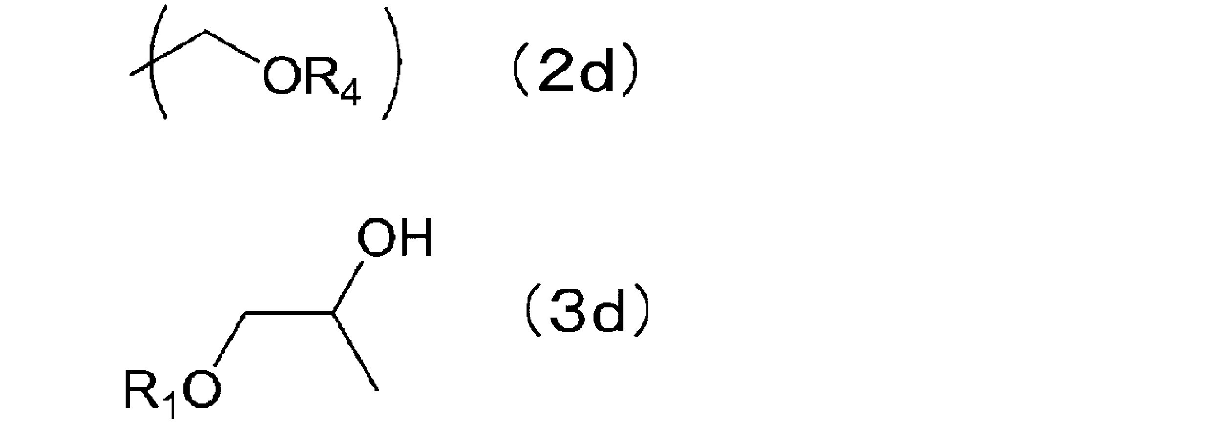
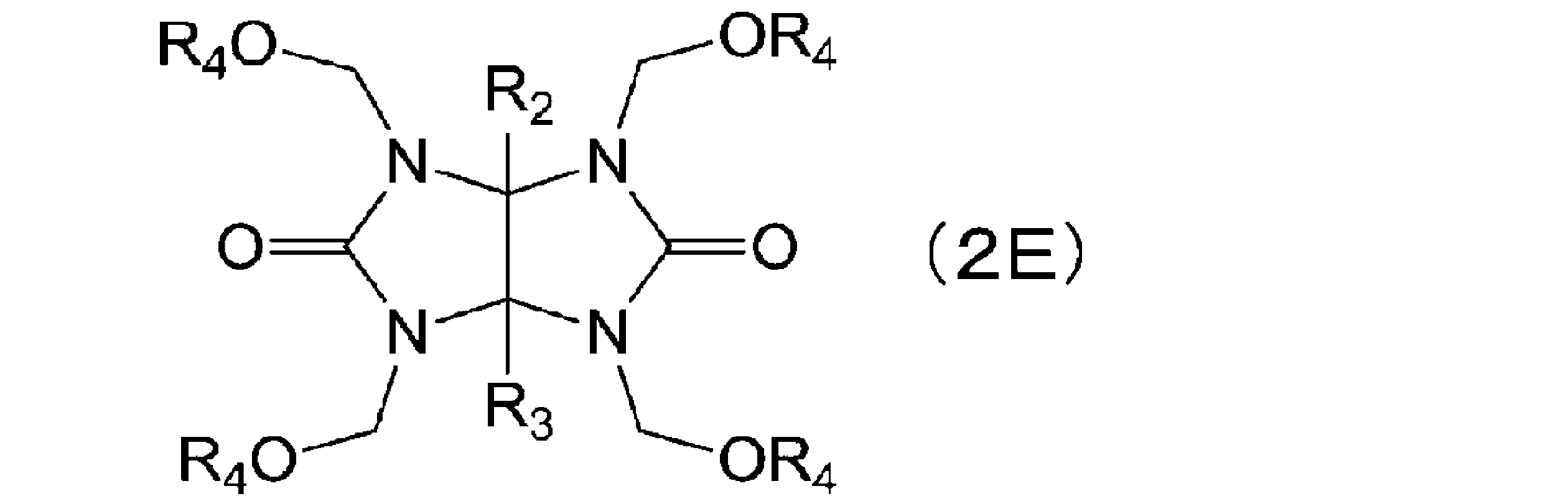


R5は、それぞれ独立して、窒素原子、又は窒素原子と炭素原子数1~10のアルキレン基、炭素原子数6~40のアリーレン基(該アルキレン基及びアリーレン基は、1つ又は2つ以上のアミド基又はアミノ基で任意に置換されていても良い)、酸素原子、カルボニル基、イオウ原子、-C(O)-NRa-及び-NRb-からなる群から選択される少なくとも一つ以上の基との組み合わせからなる3価の基を表し、
R2、R2a、R4、及びR6は、それぞれ独立して水素原子、炭素原子数1~10のアルキル基、又は水素原子と、炭素原子数1~10のアルキレン基、酸素原子、カルボニル基、-C(O)-NRa-及び-NRb-からなる群から選択される少なくとも一つ以上の基との組み合わせからなる1価の基を表し、
Raは水素原子又は炭素原子数1~10のアルキル基を表し、
Rbは、水素原子、炭素原子数1~10のアルキル基又は炭素原子数1~10のアルキルカルボニル基を表し、
nは1~10の繰り返し単位数を表し、及び
点線は隣接原子との化学結合を表す。)
またポリシロキサンは、一例として加水分解性シランの加水分解縮合物であってもよいし、加水分解縮合物が有するシラノール基の少なくとも一部がアルコール変性された又はアセタール保護された変性物(以下、「加水分解縮合物の変性物」と称することがある。)であってもよい。加水分解縮合物に係る加水分解性シランは、一種又は二種以上の加水分解性シランを含むことができる。
ポリシロキサンは、かご型、ラダー型、直鎖型、及び分岐型のいずれの主鎖を有する構造であるものとすることができる。さらに市販のポリシロキサンを使用することができる。

またR2は、ケイ素原子に結合する基又は原子であって、互いに独立して、アルコキシ基、アラルキルオキシ基、アシルオキシ基、又はハロゲン原子を表す。
aは0~3の整数を表す。
式(11)中のR2における各基及び原子の具体例、並びにそれらの好適な炭素数としては、式(A-1)及び(A-2)中のXについて前述した基及び原子並びに炭素数を挙げることができる。
(A)多官能エポキシ(メタ)アクリレート化合物、
(B)多官能チオール化合物、及び
(C)ラジカル重合開始剤を更に含有するものであってよい。
上記(A)成分がビスフェノール型多官能エポキシ(メタ)アクリレート化合物であってよい。
上記(B)成分が25℃で液状であってよい。
更に、(D)重合禁止剤を含有してよい。
前記光重合性物質がカチオン重合可能な反応性基を少なくとも一つ有する化合物であり、前記カチオン重合開始剤が光カチオン重合開始剤であってよい。
前記光重合性物質がラジカル重合可能な反応性基を少なくとも一つ有する化合物であり、前記光重合開始剤が光ラジカル重合開始剤であってよい。
前記糖化合物が単糖類又は二糖類化合物であってよい。
前記糖化合物が式(10):

前記脂環式エポキシ化合物がシクロアルキレンオキシド誘導体であってよい。
前記脂環式エポキシ化合物が式(2)又は式(3):
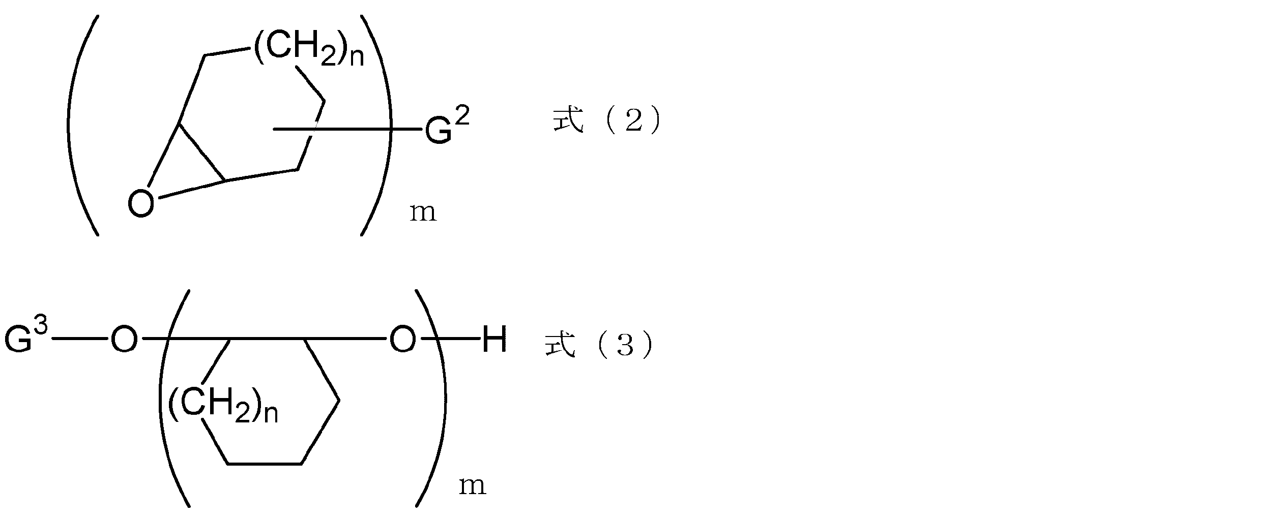
本発明に係る光硬化性樹脂組成物を半導体基板上に塗布し、塗布された組成物を焼成することによりレジスト下層膜を製造し、これを利用して半導体装置を製造することができる。

R1及びR2は、それぞれ独立に、フッ素原子又はパーフルオロアルキル基を表す。
L1は、-O-、-S-、-COO-、-SO2-、又は、-SO3-を表す。
L2は、置換基を有していてもよいアルキレン基又は単結合を表す。
W1は、置換基を有していてもよい環状有機基を表す。
M+は、カチオンを表す。

(式(31)中、Arは、炭素数6~20のアレーンから(n+1)個の水素原子を除いた基である。R1は、ヒドロキシ基、スルファニル基又は炭素数1~20の1価の有機基である。nは、0~11の整数である。nが2以上の場合、複数のR1は同一又は異なる。R2は、水素原子、フッ素原子、メチル基又はトリフルオロメチル基である。式(32)中、R3は、上記酸解離性基を含む炭素数1~20の1価の基である。Zは、単結合、酸素原子又は硫黄原子である。R4は、水素原子、フッ素原子、メチル基又はトリフルオロメチル基である。)
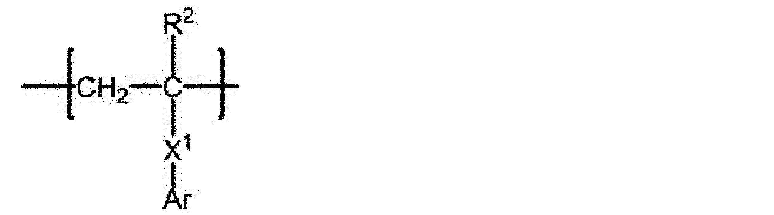
R2は、ハロゲン原子を有してもよい炭素数1~6のアルキル基、水素原子又はハロゲン原子を表し、X1は、単結合、-CO-O-*又は-CO-NR4-*を表し、*は-Arとの結合手を表し、R4は、水素原子又は炭素数1~4のアルキル基を表し、Arは、ヒドロキシ基及びカルボキシル基からなる群から選ばれる1以上の基を有していてもよい炭素数6~20の芳香族炭化水素基を表す。]
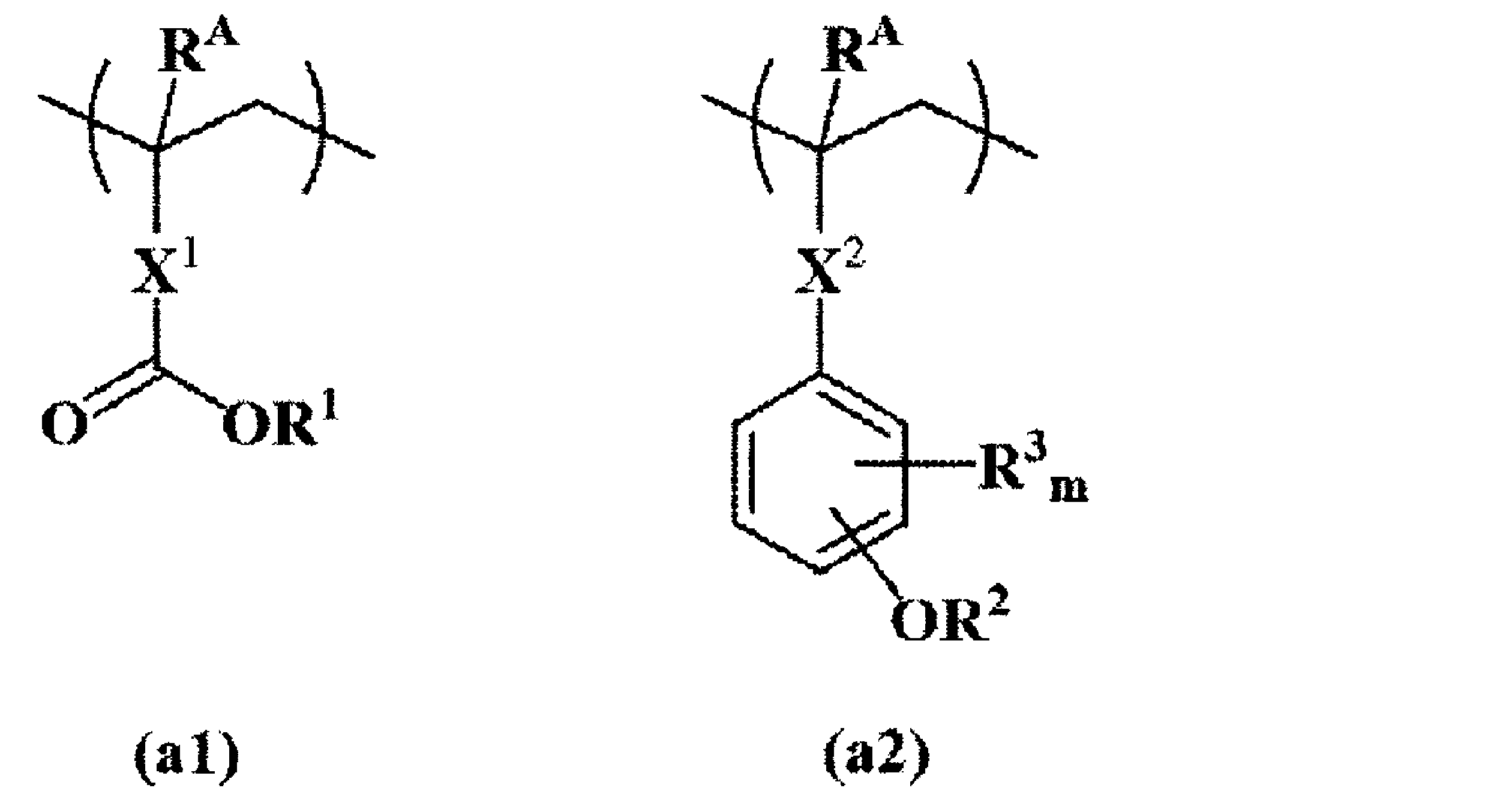
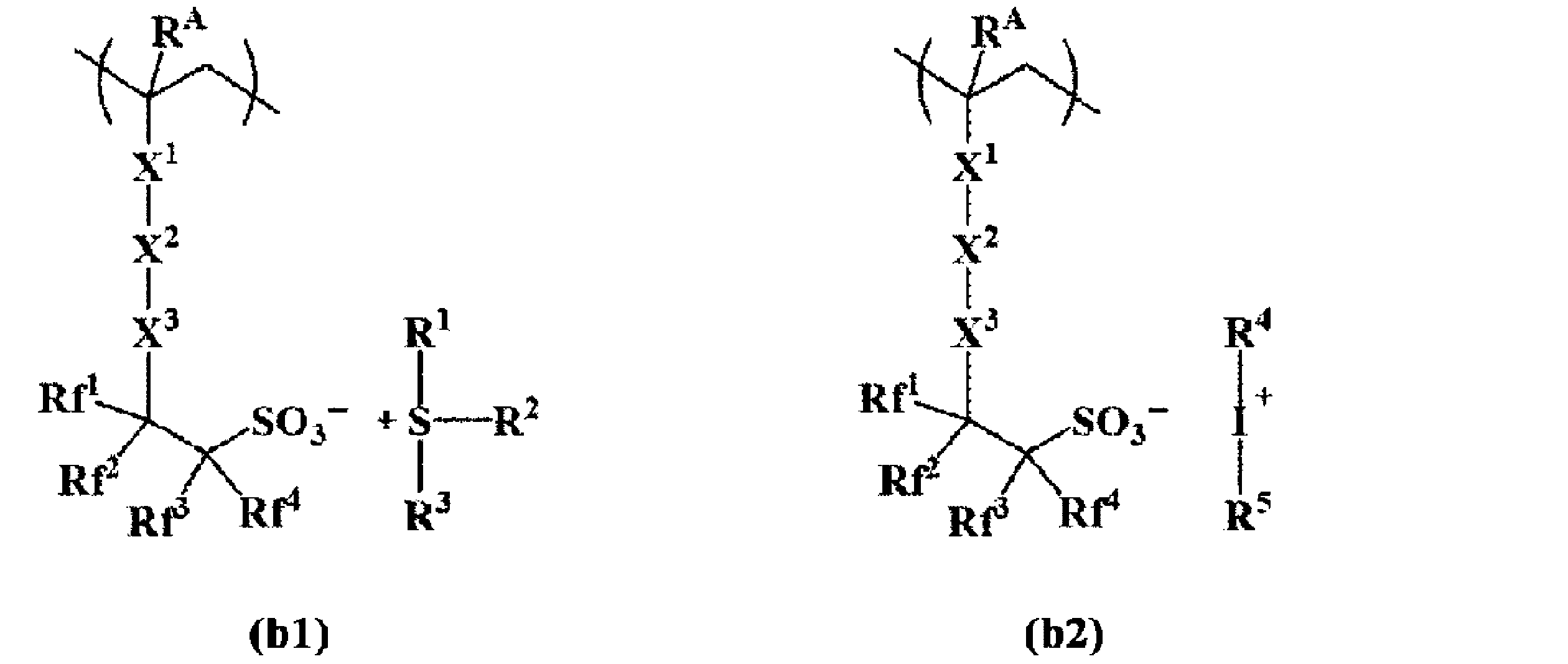

露光により酸を発生し、酸の作用により現像液に対する溶解性が変化するレジスト組成物であって、
酸の作用により現像液に対する溶解性が変化する基材成分(A)及びアルカリ現像液に対して分解性を示すフッ素添加剤成分(F)を含有し、
前記フッ素添加剤成分(F)は、塩基解離性基を含む構成単位(f1)と、下記一般式(f2-r-1)で表される基を含む構成単位(f2)と、を有するフッ素樹脂成分(F1)を含有することを特徴とする、レジスト組成物。

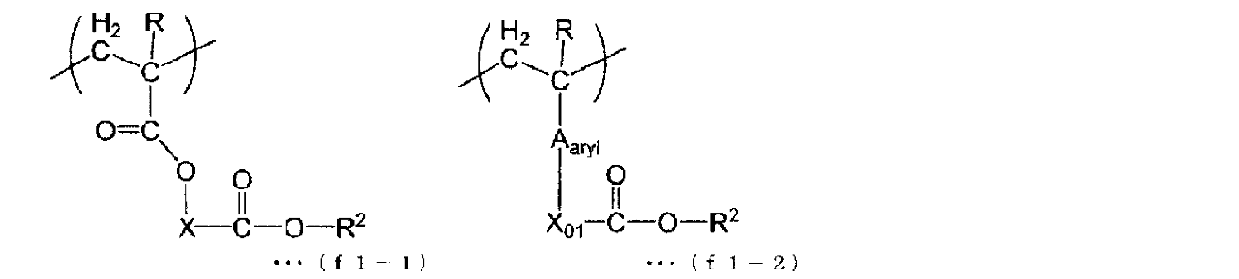
本発明に係る光硬化性樹脂組成物は、半導体製造用ウエハ端部保護膜を形成するために用いることもできる。
以下に、本発明に係る光硬化性樹脂組成物を、半導体製造用ウエハ端部保護膜を形成するために使用する場合について説明する。
(A) 半導体基板上にレジスト膜を形成する工程と、
(B) レジスト膜に対する光又は電子線の照射とその後の現像によりレジストパターンを形成する工程と、
(C) 半導体基板をエッチングで加工する工程と、
を含む半導体装置の製造方法において、
半導体製造用ウエハの表面端部と、任意選択的にベベル部及び/又は裏面端部に、
本発明に係る光硬化性樹脂組成物からの保護膜を形成する工程(X)
を含む、
半導体装置の製造方法である。
[(A)半導体基板上にレジスト膜を形成する工程]
半導体基板上にレジスト膜を形成する。半導体基板は、半導体素子等の製造のために使用されるウエハであり、一般的に用いられるシリコンウェハー、ゲルマニウムウェハーの他、例えば、ヒ化ガリウム、リン化インジウム、窒化ガリウム、窒化インジウム、窒化アルミニウム等の2種類以上の元素が結合してできる化合物半導体ウエハが使用できる。これらは通常円盤状であり、大きさは例えば4、6、8、12インチ等である。市販品を使用してよい。
レジスト膜の平均厚さの下限は、好ましくは1nm、より好ましくは3nm、5nm、10nmである。レジスト膜の平均厚さの上限は、5,000nm、3,000nm、2,000nm、好ましくは1,000nm、より好ましくは500nm、200nm、更に好ましくは50nmである。
半導体製造用ウエハの表面端部と、任意選択的にベベル部及び/又は裏面端部に、光硬化性樹脂組成物からの保護膜を形成する工程(X)を任意の時点で行う。工程(X)においては、好ましくは、光硬化性樹脂組成物を塗布し、所定の領域に露光、現像を行う。工程(X)は、工程(A)の前に行ってもよく、工程(A)と工程(B)との間に行ってもよく、工程(B)又は工程(C)の後に行ってもよい。
・光硬化性樹脂組成物の粘度:約100cps以下
・ウエハの回転速度:
・・光硬化性樹脂組成物供給時:50~500rpm
・・乾燥振り切り時:700~2,000rpm
・保護膜厚み:300nm
好ましくは170~800nm(より好ましくは200~600nm、更に好ましくは300~500nm)の波長の光で光硬化性樹脂組成物を硬化させる。
保護膜の平均厚さの下限は、例えば1nm、3nm、5nm、10nm、30nm、50nm、80nm、100nm、150nm、200nmである。保護膜の平均厚さの上限は、例えば10μm、8μm、5μm、3μm、1μm、800nm、500nm、300nmである。
レジスト膜に対する露光は、所定のパターンを形成するためのマスク(レチクル)を通して行われ、例えば、i線、KrFエキシマレーザー、ArFエキシマレーザー、EUV(極端紫外線)またはEB(電子線)が使用される。なお、露光前にソフトベーク(SB)を行ってもよく、露光後現像前に露光後加熱(PEB)を行ってもよい。露光後加熱の温度は50℃~150℃、露光後加熱の時間は1分~10分が好ましい。
ベーク温度は通常40℃~300℃、好ましくは200~300℃で1~30分間であるが、レジストパターンのダメージを避ける必要がある場合には90℃以下に設定してもよい。
上記半導体基板を加工するためのエッチングは、公知の方法であってよく、例えば半導体基板がシリコン基板である場合は、4フッ化炭素等のフッ素系ガスを用いてドライエッチングにより形状加工する工程の他、半導体基板表面に存在する窒化ケイ素膜を熱リン酸で除去する等の表面処理工程も含む。
本発明に係る半導体製造用ウエハの製造方法は、上記のような半導体装置の製造方法において、本発明に係る光硬化性樹脂組成物を、半導体製造用ウエハ前駆体の表面端部と、任意選択的にベベル部及び/又は裏面端部に施用(又は塗布)し、保護膜付き半導体製造用ウエハを製造する工程を含む。
半導体装置製造プロセスを1工程以上経て得た、半導体製造用ウエハ前駆体の表面端部と、任意選択的にベベル部及び/又は裏面端部に、半導体製造用ウエハ端部保護膜形成用組成物としての本発明に係る光硬化性樹脂組成物をスピンコートにより塗布する。
前記光硬化性樹脂組成物を塗布した後、保護膜端面にエッジビード除去、バックリンス等、半導体製造プロセスにおける公知の処理を行ってよい。
本発明の半導体製造用ウエハは、ウエハ端部が保護された半導体製造用ウエハであって、ウエハ端部に、架橋性基を有するポリマー及び溶剤を含む前記光硬化性樹脂組成物を塗布して形成した、半導体製造用ウエハである。
本明細書の下記合成例、比較合成例に示すポリマーの重量平均分子量は、ゲルパーミエーションクロマトグラフィー(以下、GPCと略称する)による測定結果である。測定には東ソー(株)製GPC装置を用い、測定条件等は次のとおりである。
GPCカラム:Shodex KF803L、Shodex KF802、Shodex KF801〔登録商標〕(昭和電工(株))
カラム温度:40℃
溶媒:テトラヒドロフラン(THF)
流量:1.0ml/分
標準試料:ポリスチレン(東ソー(株)製)
<合成例1>
グリシジルメタクリレート21gと2-ヒドロキシプロピルメタクリレート39gをプロピレングリコールモノメチルエーテル242gに溶解させた後、70℃まで昇温させた。その後、反応液を70℃に保ちながらアゾビスイソブチロニトリル0.6gを添加し、70℃で24時間反応させ、グリシジルメタクリレートと2-ヒドロキシプロピルメタクリレートの共重合高分子化合物の溶液を得た。得られた共重合高分子化合物のGPC分析を行ったところ、標準ポリスチレン換算にて重量平均分子量は50,000であった。その高分子化合物20gを有する溶液100gに、9-アントラセンカルボン酸10g、ベンジルトリエチルアンモニウムクロリド0.3g、及びプロピレングリコールモノメチルエーテル41gを添加し、130℃で24時間反応させ、式(S1)の高分子化合物の溶液を得た。

クレゾールノボラック樹脂(旭チバ(株)製品、商品名ECN1299、重量平均分子量3,900)10gをプロピレングリコールモノメチルエーテル80gに添加し溶解させた。その溶液に、9-アントラセンカルボン酸9.7gとベンジルトリエチルアンモニウムクロリド0.26gを添加した後、105℃で24時間反応させ、式(S2)の樹脂化合物を得た。得られた樹脂化合物のGPC分析を行ったところ、標準ポリスチレン換算にて重量平均分子量は5,600であった。
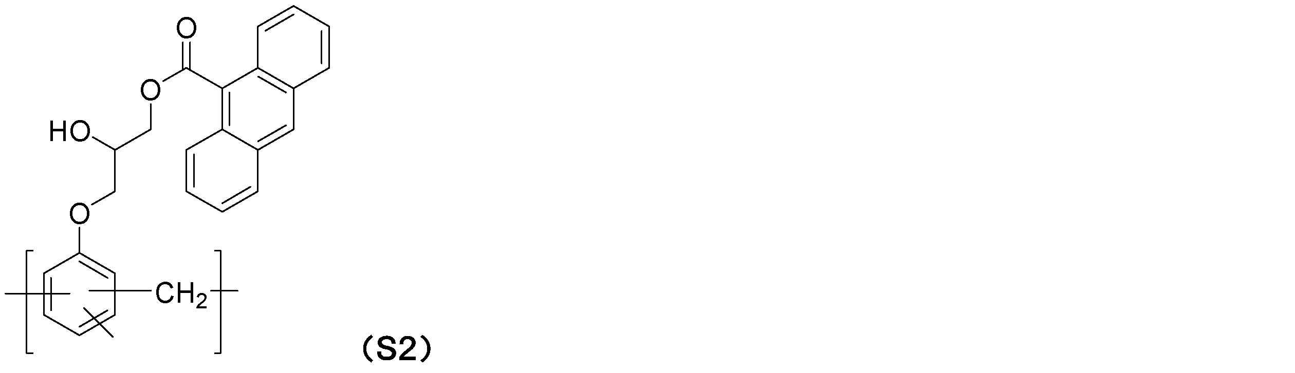
γ―ブチロラクトンメタクリレート6.6g(0.039モル)、ヒドロキシプロピルメタクリレート6.6g(0.046モル)およびベンジルメタクリレート6.8g(0.039モル)、アゾビスイソブチロニトリル0.2gを乳酸エチル80.4gに溶解させた後、フラスコ内を窒素にて置換し、70℃まで昇温し、24時間反応させ式(S3)の樹脂を得た。

9-アントリルメチルメタクリレート5.0g(0.018モル)、ヒドロキシプロピルメタクリレート4.8g(0.034モル)、2,2’-アゾビス(イソ酪酸)ジメチル0.2gをプロピレングリコールモノメチルエーテルアセテート40.2gに溶解させた後、フラスコ内を窒素にて置換し70℃まで昇温し、24時間反応させ、式(S4)の樹脂を得た。
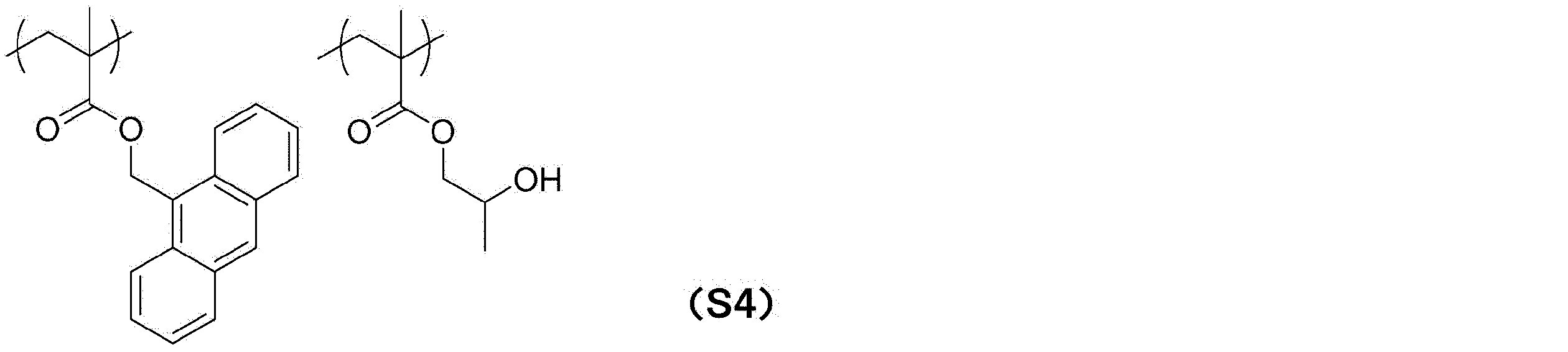
<実施例1(組成物1)、実施例2(組成物2)、実施例3(組成物3)>
合成例1、合成例2および合成例4で得た反応生成物の各々を0.24g含む溶液1.2gにプロピレングリコールモノメチルエーテル5.76gを加えた後、孔径0.10μmのポリエチレン製ミクロフィルターを用いて濾過して光硬化性樹脂組成物を調製した。
合成例3で得た反応生成物0.24gを含む溶液1.2gにプロピレングリコールモノメチルエーテル5.76gを加えた後、孔径0.10μmのポリエチレン製ミクロフィルターを用いて濾過して光硬化性樹脂組成物を調製した。
実施例1、実施例2及び比較例1で調製した光硬化性樹脂組成物の各々をスピナーにより、シリコンウェハー上に塗布した。ホットプレート上で80℃1分間焼成し、その後i線アライナー(PLA-501 キヤノン(株))により365nmの波長の光を3J/cm2照射することにより光硬化膜(膜厚0.10μm)を形成した。この光硬化膜をフォトレジストに使用する溶剤、例えばシクロヘキサノンに浸漬した。実施例1及び実施例2の組成物からの光硬化膜が溶剤に不溶であることを確認したが、比較例1の組成物からの光硬化膜は溶剤により溶解した。
実施例1、実施例2及び比較例1で調製した光硬化性樹脂組成物の各々をスピナーにより、シリコンウェハー上に塗布した。ホットプレート上で80℃1分間焼成し、その後i線アライナー(PLA-501 キヤノン(株))により、365nmの波長の光を0.3J/cm2及び3J/cm2の各強度で照射することにより光硬化膜(膜厚0.10μm)を形成した。そして、分光エリプソメーターを用い、これらの光硬化膜の波長248nmでの屈折率(n値)及び減衰係数(k値)を測定した。結果を以下に示す。(n/kの順での表記)

実施例1、実施例2及び比較例1で調製した光硬化性樹脂組成物の各々をスピナーにより、シリコンウェハー上に塗布した。ホットプレート上で80℃1分間焼成し、その後i線アライナー(PLA-501 キヤノン(株))により、365nmの波長の光を0.3J/cm2及び3J/cm2の各強度で照射することにより光硬化膜(膜厚0.10μm)を形成した。そして、サムコ製エッチャー(RIE―10NR)を用い、ドライエッチングガスとしてCF4を使用した条件下で、これらの光硬化膜のドライエッチング速度(nm/min)を測定した。
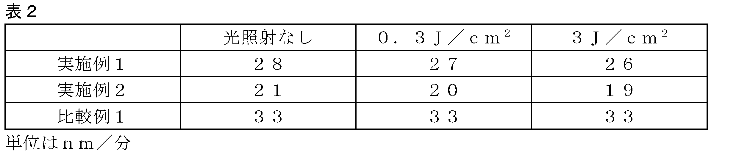
実施例1、実施例2及び比較例1で調製した光硬化性樹脂組成物の各々をスピナーにより、12インチシリコンウェハー上に塗布した。ホットプレート上で80℃1分間焼成し、その後Lithiuspro(東京エレクトロン(株))のWEEによりウェハエッジを50mJ/cm2照射することにより、光硬化膜(膜厚0.30μm)を形成した。この光硬化膜をフォトレジストに使用する溶剤、例えばOK73シンナーに浸漬した。実施例1及び実施例2の光硬化膜が溶剤に不溶であることを確認したが、比較例1の光硬化膜は溶剤により溶解した。
また、当該組成物の光硬化膜、特に半導体製造用ウエハ端部保護膜、当該光硬化膜を有する半導体製造用ウエハ、並びに光硬化性樹脂組成物を利用した積層基板、及び半導体装置の製造方法を提供することができる。
Claims (16)
- 多環芳香族炭化水素基を含有するポリマー及び/又は化合物、並びに溶剤を含む、光硬化性樹脂組成物。
- 前記多環芳香族炭化水素基が、ナフタレン、アントラセン、フェナントレン及びピレンからなる群より選ばれる少なくとも1種に由来する、請求項1に記載の光硬化性樹脂組成物。
- 前記ポリマーが、それぞれ多環芳香族炭化水素基を含有するポリビニルアルコール、ポリアクリルアミド、(メタ)アクリル系樹脂、ポリアミド酸、ポリヒドロキシスチレン、ポリヒドロキシスチレン誘導体、ポリメタクリレートとマレイン酸無水物との共重合体、エポキシ樹脂、フェノール樹脂、ノボラック樹脂、ポリイミド、セルロース、セルロース誘導体、スターチ、キチン、キトサン、ゼラチン、ゼイン、糖骨格高分子化合物、ポリアミド、ポリエチレンテレフタレート、ポリカーボネート、ポリウレタン及びポリシロキサンからなる群より選ばれる少なくとも1種である、請求項1に記載の光硬化性樹脂組成物。
- 前記化合物が、複素環構造を更に含む、請求項1に記載の光硬化性樹脂組成物。
- 170~800nmの波長の光で硬化する、請求項1に記載の光硬化性樹脂組成物。
- 半導体製造用ウエハ端部保護膜を形成するための、請求項1に記載の光硬化性樹脂組成物。
- 25℃において100cps以下の粘度を有する、請求項6に記載の光硬化性樹脂組成物。
- 請求項1~7何れか1項に記載の光硬化性樹脂組成物からなる塗布膜の光硬化膜。
- 請求項6又は7に記載の光硬化性樹脂組成物からなる塗布膜の光硬化物である半導体製造用ウエハ端部保護膜。
- 1nm~10μmの厚みを有する、請求項9に記載の半導体製造用ウエハ端部保護膜。
- ウエハ端部の金属汚染を防止するための、請求項9に記載の半導体製造用ウエハ端部保護膜。
- 半導体製造用ウエハの端部に、請求項9に記載の半導体製造用ウエハ端部保護膜を有する、半導体製造用ウエハ。
- 半導体製造用ウエハ端部保護膜を形成するための、請求項1~7何れか1項に記載の光硬化性樹脂組成物の使用。
- 基板上に、請求項1~7何れか1項に記載の光硬化性樹脂組成物を塗布する工程、及び塗布された組成物を露光する工程を含む、積層基板の製造方法。
- 前記基板が、段差を有する、請求項14に記載の積層基板の製造方法。
- 基板上に、請求項1~7何れか1項に記載の光硬化性樹脂組成物を塗布する工程、及び塗布された組成物を露光する工程を含む、半導体装置の製造方法。
Priority Applications (5)
| Application Number | Priority Date | Filing Date | Title |
|---|---|---|---|
| EP22892912.1A EP4435517A4 (en) | 2021-11-15 | 2022-11-14 | Polycyclic aromatic hydrocarbon-based light-curable resin composition |
| US18/709,974 US20250011507A1 (en) | 2021-11-15 | 2022-11-14 | Polycyclic aromatic hydrocarbon photocurable resin composition |
| JP2023559937A JPWO2023085414A1 (ja) | 2021-11-15 | 2022-11-14 | |
| CN202280075471.1A CN118235092A (zh) | 2021-11-15 | 2022-11-14 | 多环芳香族烃系光固化性树脂组合物 |
| KR1020247019082A KR20240104152A (ko) | 2021-11-15 | 2022-11-14 | 다환 방향족 탄화수소계 광 경화성 수지 조성물 |
Applications Claiming Priority (2)
| Application Number | Priority Date | Filing Date | Title |
|---|---|---|---|
| JP2021185496 | 2021-11-15 | ||
| JP2021-185496 | 2021-11-15 |
Publications (1)
| Publication Number | Publication Date |
|---|---|
| WO2023085414A1 true WO2023085414A1 (ja) | 2023-05-19 |
Family
ID=86335858
Family Applications (1)
| Application Number | Title | Priority Date | Filing Date |
|---|---|---|---|
| PCT/JP2022/042164 Ceased WO2023085414A1 (ja) | 2021-11-15 | 2022-11-14 | 多環芳香族炭化水素系光硬化性樹脂組成物 |
Country Status (7)
| Country | Link |
|---|---|
| US (1) | US20250011507A1 (ja) |
| EP (1) | EP4435517A4 (ja) |
| JP (1) | JPWO2023085414A1 (ja) |
| KR (1) | KR20240104152A (ja) |
| CN (1) | CN118235092A (ja) |
| TW (1) | TW202337929A (ja) |
| WO (1) | WO2023085414A1 (ja) |
Cited By (4)
| Publication number | Priority date | Publication date | Assignee | Title |
|---|---|---|---|---|
| KR102789050B1 (ko) * | 2023-12-13 | 2025-04-01 | 충남대학교산학협력단 | 폴리비닐알코올 기반 감광가역성 고분자를 포함하는 감광가역성 포토레지스트 조성물 및 이의 제조방법 |
| KR102789059B1 (ko) * | 2023-12-13 | 2025-04-01 | 충남대학교산학협력단 | 셀룰로오스 기반 감광가역성 고분자를 포함하는 감광가역성 포토레지스트 조성물 및 이의 제조방법 |
| WO2025068373A1 (en) * | 2023-09-29 | 2025-04-03 | Merck Patent Gmbh | Lithography compositions and methods of use thereof for sustainable and greener solutions for edge protection layers |
| CN120428521A (zh) * | 2025-07-04 | 2025-08-05 | 湖南初源新材料股份有限公司 | 含有蒽甲基修饰壳聚糖光敏剂的感光树脂组合物及其应用 |
Families Citing this family (1)
| Publication number | Priority date | Publication date | Assignee | Title |
|---|---|---|---|---|
| TWI913135B (zh) * | 2025-03-14 | 2026-01-21 | 奇美實業股份有限公司 | 負型感光性樹脂組成物及光阻圖案的形成方法 |
Citations (68)
| Publication number | Priority date | Publication date | Assignee | Title |
|---|---|---|---|---|
| JPS57177139A (en) * | 1981-04-02 | 1982-10-30 | Ciba Geigy Ag | Method of forming picture |
| JPH10186647A (ja) * | 1996-10-07 | 1998-07-14 | Shipley Co Llc | 染色されたフォトレジストとその方法及びそれからなる工業製品 |
| WO2009104643A1 (ja) | 2008-02-20 | 2009-08-27 | 日産化学工業株式会社 | 光硬化膜形成組成物及び光硬化膜形成方法 |
| JP2010128369A (ja) | 2008-11-28 | 2010-06-10 | Tokyo Ohka Kogyo Co Ltd | ポジ型レジスト組成物及びレジストパターン形成方法 |
| JP2010181857A (ja) | 2008-08-13 | 2010-08-19 | Tokyo Ohka Kogyo Co Ltd | ポジ型レジスト組成物及びレジストパターン形成方法、並びに高分子化合物 |
| JP2011043749A (ja) | 2009-08-24 | 2011-03-03 | Tokyo Ohka Kogyo Co Ltd | ポジ型レジスト組成物、レジストパターン形成方法、高分子化合物 |
| JP2011228340A (ja) | 2010-04-15 | 2011-11-10 | Elpida Memory Inc | 半導体装置の製造方法 |
| JP2011253185A (ja) | 2010-06-01 | 2011-12-15 | Inpria Corp | パターン形成された無機層、放射線によるパターン形成組成物、およびそれに対応する方法 |
| JP2012022261A (ja) | 2010-06-15 | 2012-02-02 | Tokyo Ohka Kogyo Co Ltd | ポジ型レジスト組成物、レジストパターン形成方法 |
| JP2012022258A (ja) | 2010-07-16 | 2012-02-02 | Tokyo Ohka Kogyo Co Ltd | ポジ型レジスト組成物、レジストパターン形成方法 |
| JP2012168279A (ja) | 2011-02-10 | 2012-09-06 | Tokyo Ohka Kogyo Co Ltd | Euv用レジスト組成物、euv用レジスト組成物の製造方法、およびレジストパターン形成方法 |
| JP2015010878A (ja) | 2013-06-27 | 2015-01-19 | 日本精機株式会社 | 液面位置検出装置及び液面位置検出方法 |
| WO2015026482A2 (en) | 2013-08-22 | 2015-02-26 | Inpria Corporation | Organometallic solution based high resolution patterning compositions |
| US20150357571A1 (en) * | 2012-11-30 | 2015-12-10 | Lg Display Co., Ltd. | Photoresist Employing Photodimerization Chemistry and Method for Manufacturing Organic Light Emitting Diode Display Using the Same |
| JP2016003160A (ja) | 2014-06-17 | 2016-01-12 | 日産化学工業株式会社 | ガラス保護膜形成用組成物及びガラス保護膜 |
| JP2016035570A (ja) | 2014-07-31 | 2016-03-17 | 住友化学株式会社 | レジスト組成物 |
| JP2016035567A (ja) | 2014-07-31 | 2016-03-17 | 住友化学株式会社 | レジスト組成物 |
| JP2016035565A (ja) | 2014-07-31 | 2016-03-17 | 住友化学株式会社 | レジスト組成物 |
| JP2016047920A (ja) | 2014-08-25 | 2016-04-07 | 住友化学株式会社 | 塩、樹脂、レジスト組成物及びレジストパターンの製造方法 |
| WO2016065120A1 (en) | 2014-10-23 | 2016-04-28 | Inpria Corporation | Organometallic solution based high resolution patterning compositions and corresponding methods |
| JP2016090441A (ja) | 2014-11-06 | 2016-05-23 | 東京応化工業株式会社 | 電子銃の電子線照射量の安定化方法、及びアウトガス評価方法 |
| JP2016108325A (ja) | 2014-11-26 | 2016-06-20 | 住友化学株式会社 | 塩、樹脂、レジスト組成物及びレジストパターンの製造方法 |
| JP2016130240A (ja) | 2015-01-08 | 2016-07-21 | 住友化学株式会社 | 塩、酸発生剤、レジスト組成物及びレジストパターンの製造方法 |
| JP2016153409A (ja) | 2010-08-27 | 2016-08-25 | 住友化学株式会社 | 塩、レジスト組成物及びレジストパターンの製造方法 |
| WO2017066319A2 (en) | 2015-10-13 | 2017-04-20 | Inpria Corporation | Organotin oxide hydroxide patterning compositions, precursors, and patterning |
| JP2017098333A (ja) | 2015-11-19 | 2017-06-01 | 東京エレクトロン株式会社 | 基板処理方法 |
| WO2017156388A1 (en) | 2016-03-11 | 2017-09-14 | Inpria Corporation | Pre-patterned lithography templates, processes based on radiation patterning using the templates and processes to form the templates |
| WO2017187969A1 (ja) | 2016-04-28 | 2017-11-02 | 日産化学工業株式会社 | レジスト下層膜形成組成物 |
| JP2018022039A (ja) | 2016-08-03 | 2018-02-08 | 東京応化工業株式会社 | レジスト組成物及びレジストパターン形成方法 |
| WO2018031896A1 (en) | 2016-08-12 | 2018-02-15 | Inpria Corporation | Methods of reducing metal residue in edge bead region from metal-containing resists |
| JP2018028090A (ja) | 2012-08-08 | 2018-02-22 | 住友化学株式会社 | 塩、レジスト組成物及びレジストパターンの製造方法 |
| JP2018045152A (ja) | 2016-09-15 | 2018-03-22 | 東京応化工業株式会社 | レジスト組成物及びレジストパターン形成方法 |
| JP2018070596A (ja) | 2016-10-21 | 2018-05-10 | 住友化学株式会社 | 塩、酸発生剤、レジスト組成物及びレジストパターンの製造方法 |
| WO2018190088A1 (ja) | 2017-04-11 | 2018-10-18 | Jsr株式会社 | 感放射線性組成物及びレジストパターン形成方法 |
| WO2018190380A1 (ja) | 2017-04-14 | 2018-10-18 | 日産化学株式会社 | 炭素原子間の不飽和結合によるプラズマ硬化性化合物を含む段差基板被覆膜形成組成物 |
| WO2018194123A1 (ja) | 2017-04-20 | 2018-10-25 | Jsr株式会社 | 感放射線性樹脂組成物及びレジストパターン形成方法 |
| WO2018193954A1 (ja) | 2017-04-21 | 2018-10-25 | 富士フイルム株式会社 | Euv光用感光性組成物、パターン形成方法、電子デバイスの製造方法 |
| JP2018180525A (ja) | 2017-04-17 | 2018-11-15 | Jsr株式会社 | 感放射線性樹脂組成物及びレジストパターンの形成方法 |
| JP2018197853A (ja) | 2017-05-22 | 2018-12-13 | 信越化学工業株式会社 | レジスト材料及びパターン形成方法 |
| WO2018230334A1 (ja) | 2017-06-15 | 2018-12-20 | Jsr株式会社 | 感放射線性樹脂組成物及びレジストパターン形成方法 |
| JP2019003176A (ja) | 2017-06-14 | 2019-01-10 | 信越化学工業株式会社 | レジスト材料及びパターン形成方法 |
| JP2019003175A (ja) | 2017-06-14 | 2019-01-10 | 信越化学工業株式会社 | レジスト材料及びパターン形成方法 |
| JP2019008280A (ja) | 2017-06-21 | 2019-01-17 | 信越化学工業株式会社 | レジスト材料及びパターン形成方法 |
| JP2019008279A (ja) | 2017-06-21 | 2019-01-17 | 信越化学工業株式会社 | レジスト材料及びパターン形成方法 |
| WO2019021975A1 (ja) | 2017-07-24 | 2019-01-31 | Jsr株式会社 | 極端紫外線又は電子線リソグラフィー用金属含有膜形成組成物、極端紫外線又は電子線リソグラフィー用金属含有膜及びパターン形成方法 |
| WO2019026549A1 (ja) | 2017-07-31 | 2019-02-07 | 富士フイルム株式会社 | 感活性光線性または感放射線性樹脂組成物、レジスト膜、パターン形成方法、電子デバイスの製造方法 |
| WO2019039290A1 (ja) | 2017-08-24 | 2019-02-28 | 富士フイルム株式会社 | 感活性光線性又は感放射線性樹脂組成物、レジスト膜、パターン形成方法、電子デバイスの製造方法、レジスト膜付きマスクブランクス、レジスト膜付きマスクブランクスのパターン形成方法 |
| WO2019044231A1 (ja) | 2017-08-31 | 2019-03-07 | 富士フイルム株式会社 | 感活性光線性又は感放射線性樹脂組成物、レジスト膜、パターン形成方法、電子デバイスの製造方法 |
| WO2019044259A1 (ja) | 2017-08-31 | 2019-03-07 | 富士フイルム株式会社 | 感活性光線性又は感放射線性樹脂組成物、レジスト膜、パターン形成方法、電子デバイスの製造方法 |
| WO2019054282A1 (ja) | 2017-09-15 | 2019-03-21 | 富士フイルム株式会社 | 感活性光線性又は感放射線性樹脂組成物、レジスト膜、パターン形成方法、電子デバイスの製造方法 |
| WO2019054420A1 (ja) * | 2017-09-13 | 2019-03-21 | 日産化学株式会社 | 硬化性官能基を有する化合物を含む段差基板被覆組成物 |
| WO2019058945A1 (ja) | 2017-09-20 | 2019-03-28 | 富士フイルム株式会社 | 感活性光線性又は感放射線性樹脂組成物、レジスト膜、パターン形成方法、及び、電子デバイスの製造方法 |
| WO2019058890A1 (ja) | 2017-09-20 | 2019-03-28 | 富士フイルム株式会社 | 感活性光線性又は感放射線性樹脂組成物、レジスト膜、パターン形成方法、及び、電子デバイスの製造方法 |
| JP2019052294A (ja) | 2017-09-13 | 2019-04-04 | 信越化学工業株式会社 | 重合性単量体、重合体、レジスト材料、及びパターン形成方法 |
| JP2019061217A (ja) | 2017-09-25 | 2019-04-18 | 信越化学工業株式会社 | レジスト材料及びパターン形成方法 |
| JP2019101417A (ja) | 2017-11-29 | 2019-06-24 | 信越化学工業株式会社 | パターン形成方法 |
| WO2019123842A1 (ja) | 2017-12-22 | 2019-06-27 | 富士フイルム株式会社 | 感活性光線性又は感放射線性樹脂組成物、レジスト膜、パターン形成方法、レジスト膜付きマスクブランクス、フォトマスクの製造方法、電子デバイスの製造方法 |
| JP2019117373A (ja) | 2017-12-27 | 2019-07-18 | 信越化学工業株式会社 | レジスト材料及びパターン形成方法 |
| WO2019167725A1 (ja) | 2018-02-28 | 2019-09-06 | 富士フイルム株式会社 | 感活性光線性又は感放射線性樹脂組成物、レジスト膜、パターン形成方法、電子デバイスの製造方法、樹脂 |
| WO2019167419A1 (ja) | 2018-02-28 | 2019-09-06 | 富士フイルム株式会社 | 感活性光線性又は感放射線性樹脂組成物、感活性光線性又は感放射線性樹脂組成物用の樹脂の製造方法、感活性光線性又は感放射線性膜、パターン形成方法、及び電子デバイスの製造方法 |
| WO2019167737A1 (ja) | 2018-02-28 | 2019-09-06 | 富士フイルム株式会社 | 感活性光線性又は感放射線性樹脂組成物、レジスト膜、パターン形成方法、電子デバイスの製造方法 |
| WO2019172054A1 (ja) | 2018-03-08 | 2019-09-12 | Jsr株式会社 | 感放射線性樹脂組成物及びその製造方法並びにレジストパターン形成方法 |
| WO2019187803A1 (ja) | 2018-03-30 | 2019-10-03 | 富士フイルム株式会社 | 感活性光線性又は感放射線性樹脂組成物、レジスト膜、パターン形成方法、電子デバイスの製造方法 |
| WO2019187881A1 (ja) | 2018-03-30 | 2019-10-03 | 富士フイルム株式会社 | Euv光用ネガ型感光性組成物、パターン形成方法、電子デバイスの製造方法 |
| WO2019188595A1 (ja) | 2018-03-26 | 2019-10-03 | 富士フイルム株式会社 | 感光性樹脂組成物及びその製造方法、レジスト膜、パターン形成方法、並びに、電子デバイスの製造方法 |
| WO2019187445A1 (ja) | 2018-03-27 | 2019-10-03 | 富士フイルム株式会社 | 感活性光線性又は感放射線性樹脂組成物、レジスト膜、パターン形成方法、及び、電子デバイスの製造方法 |
| JP2019191298A (ja) | 2018-04-20 | 2019-10-31 | 信越化学工業株式会社 | レジスト材料及びパターン形成方法 |
| WO2020071361A1 (ja) | 2018-10-05 | 2020-04-09 | 日産化学株式会社 | レジスト下層膜形成組成物及びそれを用いたレジストパターンの形成方法 |
Family Cites Families (4)
| Publication number | Priority date | Publication date | Assignee | Title |
|---|---|---|---|---|
| US5919599A (en) * | 1997-09-30 | 1999-07-06 | Brewer Science, Inc. | Thermosetting anti-reflective coatings at deep ultraviolet |
| JP6439766B2 (ja) * | 2016-09-23 | 2018-12-19 | 東京エレクトロン株式会社 | 塗布、現像方法及び塗布、現像装置 |
| JP2018124354A (ja) * | 2017-01-30 | 2018-08-09 | Jsr株式会社 | レジスト膜形成方法及び保護膜形成用組成物 |
| JP7601107B2 (ja) * | 2020-10-08 | 2024-12-17 | Jsr株式会社 | 保護膜形成用組成物、保護膜、保護膜の形成方法、及び基板の製造方法 |
-
2022
- 2022-11-14 TW TW111143337A patent/TW202337929A/zh unknown
- 2022-11-14 KR KR1020247019082A patent/KR20240104152A/ko active Pending
- 2022-11-14 US US18/709,974 patent/US20250011507A1/en active Pending
- 2022-11-14 JP JP2023559937A patent/JPWO2023085414A1/ja active Pending
- 2022-11-14 CN CN202280075471.1A patent/CN118235092A/zh active Pending
- 2022-11-14 WO PCT/JP2022/042164 patent/WO2023085414A1/ja not_active Ceased
- 2022-11-14 EP EP22892912.1A patent/EP4435517A4/en active Pending
Patent Citations (71)
| Publication number | Priority date | Publication date | Assignee | Title |
|---|---|---|---|---|
| JPS57177139A (en) * | 1981-04-02 | 1982-10-30 | Ciba Geigy Ag | Method of forming picture |
| JPH10186647A (ja) * | 1996-10-07 | 1998-07-14 | Shipley Co Llc | 染色されたフォトレジストとその方法及びそれからなる工業製品 |
| WO2009104643A1 (ja) | 2008-02-20 | 2009-08-27 | 日産化学工業株式会社 | 光硬化膜形成組成物及び光硬化膜形成方法 |
| JP2010181857A (ja) | 2008-08-13 | 2010-08-19 | Tokyo Ohka Kogyo Co Ltd | ポジ型レジスト組成物及びレジストパターン形成方法、並びに高分子化合物 |
| JP2010128369A (ja) | 2008-11-28 | 2010-06-10 | Tokyo Ohka Kogyo Co Ltd | ポジ型レジスト組成物及びレジストパターン形成方法 |
| JP2011043749A (ja) | 2009-08-24 | 2011-03-03 | Tokyo Ohka Kogyo Co Ltd | ポジ型レジスト組成物、レジストパターン形成方法、高分子化合物 |
| JP2011228340A (ja) | 2010-04-15 | 2011-11-10 | Elpida Memory Inc | 半導体装置の製造方法 |
| JP2016029498A (ja) | 2010-06-01 | 2016-03-03 | インプリア・コーポレイションInpria Corporation | パターン形成された無機層、放射線によるパターン形成組成物、およびそれに対応する方法 |
| JP2011253185A (ja) | 2010-06-01 | 2011-12-15 | Inpria Corp | パターン形成された無機層、放射線によるパターン形成組成物、およびそれに対応する方法 |
| JP2018041099A (ja) | 2010-06-01 | 2018-03-15 | インプリア・コーポレイションInpria Corporation | パターン形成された無機層、放射線によるパターン形成組成物、およびそれに対応する方法 |
| JP2012022261A (ja) | 2010-06-15 | 2012-02-02 | Tokyo Ohka Kogyo Co Ltd | ポジ型レジスト組成物、レジストパターン形成方法 |
| JP2012022258A (ja) | 2010-07-16 | 2012-02-02 | Tokyo Ohka Kogyo Co Ltd | ポジ型レジスト組成物、レジストパターン形成方法 |
| JP2016153409A (ja) | 2010-08-27 | 2016-08-25 | 住友化学株式会社 | 塩、レジスト組成物及びレジストパターンの製造方法 |
| JP2012168279A (ja) | 2011-02-10 | 2012-09-06 | Tokyo Ohka Kogyo Co Ltd | Euv用レジスト組成物、euv用レジスト組成物の製造方法、およびレジストパターン形成方法 |
| JP2018028090A (ja) | 2012-08-08 | 2018-02-22 | 住友化学株式会社 | 塩、レジスト組成物及びレジストパターンの製造方法 |
| US20150357571A1 (en) * | 2012-11-30 | 2015-12-10 | Lg Display Co., Ltd. | Photoresist Employing Photodimerization Chemistry and Method for Manufacturing Organic Light Emitting Diode Display Using the Same |
| JP2015010878A (ja) | 2013-06-27 | 2015-01-19 | 日本精機株式会社 | 液面位置検出装置及び液面位置検出方法 |
| WO2015026482A2 (en) | 2013-08-22 | 2015-02-26 | Inpria Corporation | Organometallic solution based high resolution patterning compositions |
| JP2019113855A (ja) | 2013-08-22 | 2019-07-11 | インプリア・コーポレイションInpria Corporation | 有機金属溶液に基づいた高解像度パターニング組成物 |
| JP2016003160A (ja) | 2014-06-17 | 2016-01-12 | 日産化学工業株式会社 | ガラス保護膜形成用組成物及びガラス保護膜 |
| JP2016035570A (ja) | 2014-07-31 | 2016-03-17 | 住友化学株式会社 | レジスト組成物 |
| JP2016035567A (ja) | 2014-07-31 | 2016-03-17 | 住友化学株式会社 | レジスト組成物 |
| JP2016035565A (ja) | 2014-07-31 | 2016-03-17 | 住友化学株式会社 | レジスト組成物 |
| JP2016047920A (ja) | 2014-08-25 | 2016-04-07 | 住友化学株式会社 | 塩、樹脂、レジスト組成物及びレジストパターンの製造方法 |
| WO2016065120A1 (en) | 2014-10-23 | 2016-04-28 | Inpria Corporation | Organometallic solution based high resolution patterning compositions and corresponding methods |
| JP2016090441A (ja) | 2014-11-06 | 2016-05-23 | 東京応化工業株式会社 | 電子銃の電子線照射量の安定化方法、及びアウトガス評価方法 |
| JP2016108325A (ja) | 2014-11-26 | 2016-06-20 | 住友化学株式会社 | 塩、樹脂、レジスト組成物及びレジストパターンの製造方法 |
| JP2016130240A (ja) | 2015-01-08 | 2016-07-21 | 住友化学株式会社 | 塩、酸発生剤、レジスト組成物及びレジストパターンの製造方法 |
| WO2017066319A2 (en) | 2015-10-13 | 2017-04-20 | Inpria Corporation | Organotin oxide hydroxide patterning compositions, precursors, and patterning |
| JP2017098333A (ja) | 2015-11-19 | 2017-06-01 | 東京エレクトロン株式会社 | 基板処理方法 |
| WO2017156388A1 (en) | 2016-03-11 | 2017-09-14 | Inpria Corporation | Pre-patterned lithography templates, processes based on radiation patterning using the templates and processes to form the templates |
| WO2017187969A1 (ja) | 2016-04-28 | 2017-11-02 | 日産化学工業株式会社 | レジスト下層膜形成組成物 |
| JP2018022039A (ja) | 2016-08-03 | 2018-02-08 | 東京応化工業株式会社 | レジスト組成物及びレジストパターン形成方法 |
| WO2018031896A1 (en) | 2016-08-12 | 2018-02-15 | Inpria Corporation | Methods of reducing metal residue in edge bead region from metal-containing resists |
| JP2018045152A (ja) | 2016-09-15 | 2018-03-22 | 東京応化工業株式会社 | レジスト組成物及びレジストパターン形成方法 |
| JP2018070596A (ja) | 2016-10-21 | 2018-05-10 | 住友化学株式会社 | 塩、酸発生剤、レジスト組成物及びレジストパターンの製造方法 |
| WO2018190088A1 (ja) | 2017-04-11 | 2018-10-18 | Jsr株式会社 | 感放射線性組成物及びレジストパターン形成方法 |
| WO2018190380A1 (ja) | 2017-04-14 | 2018-10-18 | 日産化学株式会社 | 炭素原子間の不飽和結合によるプラズマ硬化性化合物を含む段差基板被覆膜形成組成物 |
| JP2018180525A (ja) | 2017-04-17 | 2018-11-15 | Jsr株式会社 | 感放射線性樹脂組成物及びレジストパターンの形成方法 |
| WO2018194123A1 (ja) | 2017-04-20 | 2018-10-25 | Jsr株式会社 | 感放射線性樹脂組成物及びレジストパターン形成方法 |
| WO2018193954A1 (ja) | 2017-04-21 | 2018-10-25 | 富士フイルム株式会社 | Euv光用感光性組成物、パターン形成方法、電子デバイスの製造方法 |
| JP2018197853A (ja) | 2017-05-22 | 2018-12-13 | 信越化学工業株式会社 | レジスト材料及びパターン形成方法 |
| JP2019003176A (ja) | 2017-06-14 | 2019-01-10 | 信越化学工業株式会社 | レジスト材料及びパターン形成方法 |
| JP2019003175A (ja) | 2017-06-14 | 2019-01-10 | 信越化学工業株式会社 | レジスト材料及びパターン形成方法 |
| WO2018230334A1 (ja) | 2017-06-15 | 2018-12-20 | Jsr株式会社 | 感放射線性樹脂組成物及びレジストパターン形成方法 |
| JP2019008280A (ja) | 2017-06-21 | 2019-01-17 | 信越化学工業株式会社 | レジスト材料及びパターン形成方法 |
| JP2019008279A (ja) | 2017-06-21 | 2019-01-17 | 信越化学工業株式会社 | レジスト材料及びパターン形成方法 |
| WO2019021975A1 (ja) | 2017-07-24 | 2019-01-31 | Jsr株式会社 | 極端紫外線又は電子線リソグラフィー用金属含有膜形成組成物、極端紫外線又は電子線リソグラフィー用金属含有膜及びパターン形成方法 |
| WO2019026549A1 (ja) | 2017-07-31 | 2019-02-07 | 富士フイルム株式会社 | 感活性光線性または感放射線性樹脂組成物、レジスト膜、パターン形成方法、電子デバイスの製造方法 |
| WO2019039290A1 (ja) | 2017-08-24 | 2019-02-28 | 富士フイルム株式会社 | 感活性光線性又は感放射線性樹脂組成物、レジスト膜、パターン形成方法、電子デバイスの製造方法、レジスト膜付きマスクブランクス、レジスト膜付きマスクブランクスのパターン形成方法 |
| WO2019044231A1 (ja) | 2017-08-31 | 2019-03-07 | 富士フイルム株式会社 | 感活性光線性又は感放射線性樹脂組成物、レジスト膜、パターン形成方法、電子デバイスの製造方法 |
| WO2019044259A1 (ja) | 2017-08-31 | 2019-03-07 | 富士フイルム株式会社 | 感活性光線性又は感放射線性樹脂組成物、レジスト膜、パターン形成方法、電子デバイスの製造方法 |
| WO2019054420A1 (ja) * | 2017-09-13 | 2019-03-21 | 日産化学株式会社 | 硬化性官能基を有する化合物を含む段差基板被覆組成物 |
| JP2019052294A (ja) | 2017-09-13 | 2019-04-04 | 信越化学工業株式会社 | 重合性単量体、重合体、レジスト材料、及びパターン形成方法 |
| WO2019054282A1 (ja) | 2017-09-15 | 2019-03-21 | 富士フイルム株式会社 | 感活性光線性又は感放射線性樹脂組成物、レジスト膜、パターン形成方法、電子デバイスの製造方法 |
| WO2019058945A1 (ja) | 2017-09-20 | 2019-03-28 | 富士フイルム株式会社 | 感活性光線性又は感放射線性樹脂組成物、レジスト膜、パターン形成方法、及び、電子デバイスの製造方法 |
| WO2019058890A1 (ja) | 2017-09-20 | 2019-03-28 | 富士フイルム株式会社 | 感活性光線性又は感放射線性樹脂組成物、レジスト膜、パターン形成方法、及び、電子デバイスの製造方法 |
| JP2019061217A (ja) | 2017-09-25 | 2019-04-18 | 信越化学工業株式会社 | レジスト材料及びパターン形成方法 |
| JP2019101417A (ja) | 2017-11-29 | 2019-06-24 | 信越化学工業株式会社 | パターン形成方法 |
| WO2019123842A1 (ja) | 2017-12-22 | 2019-06-27 | 富士フイルム株式会社 | 感活性光線性又は感放射線性樹脂組成物、レジスト膜、パターン形成方法、レジスト膜付きマスクブランクス、フォトマスクの製造方法、電子デバイスの製造方法 |
| JP2019117373A (ja) | 2017-12-27 | 2019-07-18 | 信越化学工業株式会社 | レジスト材料及びパターン形成方法 |
| WO2019167725A1 (ja) | 2018-02-28 | 2019-09-06 | 富士フイルム株式会社 | 感活性光線性又は感放射線性樹脂組成物、レジスト膜、パターン形成方法、電子デバイスの製造方法、樹脂 |
| WO2019167419A1 (ja) | 2018-02-28 | 2019-09-06 | 富士フイルム株式会社 | 感活性光線性又は感放射線性樹脂組成物、感活性光線性又は感放射線性樹脂組成物用の樹脂の製造方法、感活性光線性又は感放射線性膜、パターン形成方法、及び電子デバイスの製造方法 |
| WO2019167737A1 (ja) | 2018-02-28 | 2019-09-06 | 富士フイルム株式会社 | 感活性光線性又は感放射線性樹脂組成物、レジスト膜、パターン形成方法、電子デバイスの製造方法 |
| WO2019172054A1 (ja) | 2018-03-08 | 2019-09-12 | Jsr株式会社 | 感放射線性樹脂組成物及びその製造方法並びにレジストパターン形成方法 |
| WO2019188595A1 (ja) | 2018-03-26 | 2019-10-03 | 富士フイルム株式会社 | 感光性樹脂組成物及びその製造方法、レジスト膜、パターン形成方法、並びに、電子デバイスの製造方法 |
| WO2019187445A1 (ja) | 2018-03-27 | 2019-10-03 | 富士フイルム株式会社 | 感活性光線性又は感放射線性樹脂組成物、レジスト膜、パターン形成方法、及び、電子デバイスの製造方法 |
| WO2019187803A1 (ja) | 2018-03-30 | 2019-10-03 | 富士フイルム株式会社 | 感活性光線性又は感放射線性樹脂組成物、レジスト膜、パターン形成方法、電子デバイスの製造方法 |
| WO2019187881A1 (ja) | 2018-03-30 | 2019-10-03 | 富士フイルム株式会社 | Euv光用ネガ型感光性組成物、パターン形成方法、電子デバイスの製造方法 |
| JP2019191298A (ja) | 2018-04-20 | 2019-10-31 | 信越化学工業株式会社 | レジスト材料及びパターン形成方法 |
| WO2020071361A1 (ja) | 2018-10-05 | 2020-04-09 | 日産化学株式会社 | レジスト下層膜形成組成物及びそれを用いたレジストパターンの形成方法 |
Non-Patent Citations (2)
| Title |
|---|
| PROC. SPIE, vol. 3999, 2000, pages 365 - 374 |
| See also references of EP4435517A4 |
Cited By (5)
| Publication number | Priority date | Publication date | Assignee | Title |
|---|---|---|---|---|
| WO2025068373A1 (en) * | 2023-09-29 | 2025-04-03 | Merck Patent Gmbh | Lithography compositions and methods of use thereof for sustainable and greener solutions for edge protection layers |
| KR102789050B1 (ko) * | 2023-12-13 | 2025-04-01 | 충남대학교산학협력단 | 폴리비닐알코올 기반 감광가역성 고분자를 포함하는 감광가역성 포토레지스트 조성물 및 이의 제조방법 |
| KR102789059B1 (ko) * | 2023-12-13 | 2025-04-01 | 충남대학교산학협력단 | 셀룰로오스 기반 감광가역성 고분자를 포함하는 감광가역성 포토레지스트 조성물 및 이의 제조방법 |
| CN120428521A (zh) * | 2025-07-04 | 2025-08-05 | 湖南初源新材料股份有限公司 | 含有蒽甲基修饰壳聚糖光敏剂的感光树脂组合物及其应用 |
| CN120428521B (zh) * | 2025-07-04 | 2025-09-26 | 湖南初源新材料股份有限公司 | 含有蒽甲基修饰壳聚糖光敏剂的感光树脂组合物及其应用 |
Also Published As
| Publication number | Publication date |
|---|---|
| JPWO2023085414A1 (ja) | 2023-05-19 |
| US20250011507A1 (en) | 2025-01-09 |
| CN118235092A (zh) | 2024-06-21 |
| EP4435517A4 (en) | 2025-03-19 |
| KR20240104152A (ko) | 2024-07-04 |
| EP4435517A1 (en) | 2024-09-25 |
| TW202337929A (zh) | 2023-10-01 |
Similar Documents
| Publication | Publication Date | Title |
|---|---|---|
| CN110780536B (zh) | 半导体抗蚀剂组合物及使用组合物形成图案的方法及系统 | |
| JP6810696B2 (ja) | ハードマスク組成物および半導体基板上での微細パターンの形成方法 | |
| TWI642698B (zh) | 作為硬光罩及填充材料之穩定金屬化合物、其組合物及其使用方法 | |
| JP6342998B2 (ja) | 可溶性金属酸化物カルボキシレートのスピンオン組成物及びそれらの使用方法 | |
| WO2023085414A1 (ja) | 多環芳香族炭化水素系光硬化性樹脂組成物 | |
| KR20160126970A (ko) | 레지스트 상층막 형성 조성물 및 이것을 이용한 반도체장치의 제조방법 | |
| KR20120022889A (ko) | Euv 리소그래피용 레지스트 하층막 형성 조성물 | |
| JP7647996B2 (ja) | 半導体製造用ウエハ端部保護膜形成用組成物 | |
| US12339586B2 (en) | Photocurable resin composition containing self-crosslinkable polymer | |
| WO2012081619A1 (ja) | レジスト下層膜形成組成物及びそれを用いたレジストパターンの形成方法 | |
| JP2010285403A (ja) | 架橋剤及び該架橋剤を含有するレジスト下層膜形成組成物 | |
| WO2013191203A1 (ja) | スルホン構造及びアミン構造を有するシリコン含有レジスト下層膜形成組成物 | |
| WO2023033094A1 (ja) | 半導体製造用ウエハ端部保護膜形成組成物 | |
| JP2025170256A (ja) | リソグラフィー膜形成用組成物、レジストパターン形成方法、及び回路パターン形成方法 | |
| JP2004205900A (ja) | リン系有機基含有高分子を含む反射防止膜形成組成物 | |
| JP5534205B2 (ja) | 感光性レジスト下層膜形成組成物及びレジストパターンの形成方法 | |
| WO2025127018A1 (ja) | レジスト下層膜形成用組成物 |
Legal Events
| Date | Code | Title | Description |
|---|---|---|---|
| 121 | Ep: the epo has been informed by wipo that ep was designated in this application |
Ref document number: 22892912 Country of ref document: EP Kind code of ref document: A1 |
|
| WWE | Wipo information: entry into national phase |
Ref document number: 2023559937 Country of ref document: JP |
|
| WWE | Wipo information: entry into national phase |
Ref document number: 202280075471.1 Country of ref document: CN |
|
| WWE | Wipo information: entry into national phase |
Ref document number: 18709974 Country of ref document: US |
|
| WWE | Wipo information: entry into national phase |
Ref document number: 1020247019082 Country of ref document: KR |
|
| WWE | Wipo information: entry into national phase |
Ref document number: 2022892912 Country of ref document: EP |
|
| ENP | Entry into the national phase |
Ref document number: 2022892912 Country of ref document: EP Effective date: 20240617 |