WO2023095423A1 - 半導体リレー及びこれを備えた電気回路 - Google Patents
半導体リレー及びこれを備えた電気回路 Download PDFInfo
- Publication number
- WO2023095423A1 WO2023095423A1 PCT/JP2022/034355 JP2022034355W WO2023095423A1 WO 2023095423 A1 WO2023095423 A1 WO 2023095423A1 JP 2022034355 W JP2022034355 W JP 2022034355W WO 2023095423 A1 WO2023095423 A1 WO 2023095423A1
- Authority
- WO
- WIPO (PCT)
- Prior art keywords
- mosfet
- light
- output
- wiring
- semiconductor relay
- Prior art date
- Legal status (The legal status is an assumption and is not a legal conclusion. Google has not performed a legal analysis and makes no representation as to the accuracy of the status listed.)
- Ceased
Links
Images












Classifications
-
- H—ELECTRICITY
- H10—SEMICONDUCTOR DEVICES; ELECTRIC SOLID-STATE DEVICES NOT OTHERWISE PROVIDED FOR
- H10F—INORGANIC SEMICONDUCTOR DEVICES SENSITIVE TO INFRARED RADIATION, LIGHT, ELECTROMAGNETIC RADIATION OF SHORTER WAVELENGTH OR CORPUSCULAR RADIATION
- H10F55/00—Radiation-sensitive semiconductor devices covered by groups H10F10/00, H10F19/00 or H10F30/00 being structurally associated with electric light sources and electrically or optically coupled thereto
-
- H—ELECTRICITY
- H03—ELECTRONIC CIRCUITRY
- H03K—PULSE TECHNIQUE
- H03K17/00—Electronic switching or gating, i.e. not by contact-making and –breaking
- H03K17/04—Modifications for accelerating switching
- H03K17/041—Modifications for accelerating switching without feedback from the output circuit to the control circuit
- H03K17/0412—Modifications for accelerating switching without feedback from the output circuit to the control circuit by measures taken in the control circuit
-
- H—ELECTRICITY
- H03—ELECTRONIC CIRCUITRY
- H03K—PULSE TECHNIQUE
- H03K17/00—Electronic switching or gating, i.e. not by contact-making and –breaking
- H03K17/51—Electronic switching or gating, i.e. not by contact-making and –breaking characterised by the components used
- H03K17/78—Electronic switching or gating, i.e. not by contact-making and –breaking characterised by the components used using opto-electronic devices, i.e. light-emitting and photoelectric devices electrically- or optically-coupled
- H03K17/785—Electronic switching or gating, i.e. not by contact-making and –breaking characterised by the components used using opto-electronic devices, i.e. light-emitting and photoelectric devices electrically- or optically-coupled controlling field-effect transistor switches
-
- H—ELECTRICITY
- H03—ELECTRONIC CIRCUITRY
- H03K—PULSE TECHNIQUE
- H03K2217/00—Indexing scheme related to electronic switching or gating, i.e. not by contact-making or -breaking covered by H03K17/00
- H03K2217/0054—Gating switches, e.g. pass gates
Definitions
- the present disclosure relates to a semiconductor relay and an electric circuit including the same.
- MOSFET output photocouplers and optical MOSFETs have been known as means for transmitting AC signals (see Patent Document 1, for example).
- Patent Document 1 semiconductor relays called MOSFET output photocouplers and optical MOSFETs.
- Patent Document 2 In order to solve this problem, for example, the configuration shown in Patent Document 2 has been proposed.
- a light-emitting element mounted on an input terminal and a light-receiving element mounted on an output terminal are arranged facing each other inside a sealing resin. Both the input terminal and the output terminal are bent once in the middle, and their tip portions protrude outward from the sealing resin along the lower surface of the sealing resin.
- this semiconductor relay When this semiconductor relay is mounted on a circuit board on which a signal line and a ground line are formed on the top surface, the passage point on the output side of the signal is arranged above the signal line inside the semiconductor relay. Therefore, the distance between the signal passage path and the ground line can be shortened, impedance mismatch can be suppressed, and insertion loss can be reduced.
- the distance between the light receiving element and the element mounting portion of the input terminal on which the light receiving element is mounted and the ground line or the ground plane formed on the lower surface of the circuit board can be increased. Both the ground line and the ground plane are electrically connected to the ground potential. As a result, the capacitance value of the parasitic capacitance generated between the input side of the semiconductor relay and the ground potential can be reduced, and the insertion loss can be further reduced.
- the present disclosure has been made in view of the above points, and its object is to provide a semiconductor relay capable of miniaturization and reduction of insertion loss, and an electric circuit having the same.
- a semiconductor relay mounted on a circuit board, comprising: a first input terminal; a second input terminal; a light-emitting element electrically connected to an input terminal; a light-receiving element that receives light output from the light-emitting element; a light-receiving driving element that includes the light-receiving element and outputs a driving signal; and the light-receiving driving element.
- the light-emitting element and the light-receiving element face each other with a predetermined gap, and each of the first MOSFET element and the second MOSFET element has a first surface and a second surface facing the first surface.
- the direction in which the light-receiving element and the light-emitting element face is the same as the direction in which the first surface and the second surface face, and the first element of the first MOSFET element is mounted on the first element mounting portion.
- a surface is mounted, the first surface of the second MOSFET element is mounted on the second element mounting portion, the first element mounting portion extends in the vertical direction,
- the first output-side external terminal portion extends from the first element mounting portion along the lower surface of the sealing resin and protrudes from the sealing resin, and the light-receiving driving element is the first MOSFET element.
- An electric circuit according to the present disclosure is an electric circuit including the semiconductor relay according to the present disclosure and the circuit board, wherein the circuit board includes a first wiring and a second wiring on an upper surface of a dielectric substrate. wherein the first wiring is composed of a pair of wirings provided with an interval, the second wiring is composed of a pair of wirings provided with an interval, and the first The input terminal is connected to the first wiring such that the lower surface of the first input-side external terminal portion is in contact with the upper surface of one of the pair of wirings forming the first wiring, and the second input terminal is connected to the first wiring.
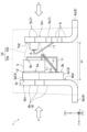
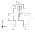
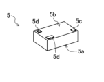
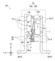
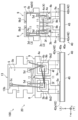
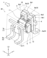
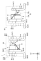
- FIG. 1 is a perspective view of a semiconductor relay according to an embodiment; FIG. It is the side view which looked at the semiconductor relay from the direction A shown in FIG. It is the figure which looked at the 1st input terminal and the 2nd input terminal in which the light emitting element was mounted from the direction B shown in FIG. It is the figure which looked at the 1st output terminal and 2nd output terminal in which the light reception drive element, the 1st MOSFET element, and the 2nd MOSFET element were mounted from the direction C shown in FIG. It is a perspective view of a light emitting element.
- 3 is a perspective view of a light receiving drive element;
- FIG. 1 is a perspective view of a first MOSFET device;
- FIG. 1 is a schematic diagram of an electrical circuit according to an embodiment; FIG.
- MOS Metal-Oxide Semiconductor Field Effect Transistor
- the X direction (first direction), Y direction (second direction), and Z direction (third direction) are orthogonal to each other.
- the term "perpendicular" means that the components forming the semiconductor relay 1 are orthogonal to each other including processing tolerances, manufacturing tolerances, and assembly tolerances between parts. It does not mean that the objects are orthogonal in a strict sense.
- the sealing resin 10 includes an insulating light-shielding resin 10a and a translucent resin 10b.
- the light-shielding resin 10a is, for example, an epoxy resin containing a black pigment. However, it is not particularly limited to this, and any material that shields light may be used.
- the translucent resin 10b is provided between the light-receiving drive element 5 and the light-emitting element 2, and is sealed with the light-shielding resin 10a.
- Translucent resin 10b is, for example, a transparent silicone resin. However, it is not particularly limited to this, and any insulating resin that is transparent to at least the light emitted by the light emitting element 2 may be used.
- the translucent resin 10b constitutes an optical coupling portion that optically couples the light receiving element 51 of the light receiving driving element 5 and the light emitting element 2. As shown in FIG.
- FIG. 8 shows a schematic diagram of an electrical circuit according to an embodiment.
- the electric circuit 100 includes at least the semiconductor relay 1 and the circuit board 40 .
- the circuit board 40 is a so-called printed wiring board in which first wirings 41, second wirings 42, and third wirings 43 are formed on the upper surface of a dielectric substrate 40a made of a dielectric material having a predetermined dielectric constant. Wiring Board).
- a ground plane 45 (see FIG. 13, for example) is formed on the lower surface of the circuit board 40 .
- Ground plane 45 is formed over substantially the entire lower surface of dielectric substrate 40a.
- the first wiring 41, the second wiring 42, the third wiring 43, and the ground plane 45 are formed by copper plating or the like on the upper or lower surface of the dielectric substrate 40a.
- the third wiring 43 and the ground plane 45 are electrically connected via a conductive via 44 (for example, see FIG. 13) that penetrates the dielectric substrate 40a in the thickness direction, in this case, the Z direction. Also, the ground plane 45 is electrically connected to the ground potential of the electric circuit 100 . In order to reduce the transmission loss of transmission signals, the relative permittivity of the dielectric substrate 40a is set low.
- the first wiring 41 is formed of a pair of parallel wirings 41a and 41b which are spaced apart in the Y direction and whose longitudinal direction is the X direction.
- the first wiring 41 is an input signal line for inputting transmission signals to the semiconductor relay 1 .
- One ends of a pair of wirings 41a and 41b forming the first wiring 41 are connected to the input side external terminal portions 6a and 7a of the first input terminal 6 and the second input terminal 7, respectively.
- the input-side external terminal portions 6a and 7a of the first input terminal 6 and the second input terminal 7 have lower surfaces that correspond to the upper surfaces of the pair of wirings 41a and 41b that form the first wiring 41, respectively. is connected to the first wiring so as to be in contact with the On the other hand, as shown in FIG.
- the other ends of the pair of wirings 41a and 41b forming the first wiring 41 are open ends.
- the second wiring 42 is provided with an interval in the Y direction, and is composed of a pair of wirings 42a and 42b whose longitudinal direction is the Y direction.
- the second wiring 42 is an output signal line for transmission signals output from the semiconductor relay 1 .
- One end of each of the pair of wirings 42a and 42b constituting the second wiring 42 is connected to the first output side external terminal portion 8a of the first output terminal 8 and the second output side external terminal portion 9a of the second output terminal 9. It is connected.
- the first output-side external terminal portion 8a of the first output terminal 8 and the second output-side external terminal portion 9a of the second output terminal 9 are paired with the second wiring 42 on the lower surfaces thereof. It is connected to the second wiring 42 so as to be in contact with the upper surface of each of 42a and 42b.
- the third wiring 43 includes two wirings 43a and 43b provided so as to sandwich the ends of the pair of wirings 41a and 41b constituting the first wiring 41, and the two wirings 43a and 43b and the second wiring. 42, and a wiring 43c provided on the opposite side in the X direction.
- the longitudinal direction of each of the three wirings 43a, 43b, 43c is the Y direction.
- the three wirings 43a, 43b, and 43c included in the third wiring 43 are also electrically connected to the ground potential through the ground plane 45.
- FIG. 8 shows an example in which only the semiconductor relay 1 is mounted on the circuit board 40, it goes without saying that other elements may be mounted on the circuit board 40 as well.
- FIG. 9 shows an equivalent circuit diagram of the semiconductor relay 1. As shown in FIG. 9
- a current is generated by photoelectric conversion in the light receiving element 51, and the driving circuit 52 operates based on this current.
- a drive signal which is a voltage signal corresponding to the light intensity of the light emitting element 2, is applied to the first gate terminal 3e of the first MOSFET element 3 and the second gate terminal 4e of the second MOSFET element 4 via the wire 11, respectively.
- the source (S)-drain (D) of the first MOSFET element 3 and the source (S) of the second MOSFET element 4 -drain (D) are turned on. Furthermore, the first output terminal 8 and the second output terminal 9 are electrically connected through the first MOSFET element 3 and the second MOSFET element 4 . As a result, the transmission signal input between the first input terminal 6 and the second input terminal 7 is transmitted between the first output terminal 8 and the second output terminal 9, and the second wiring 42 is transmitted to
- the conventional semiconductor relay 20 shown in FIG. 10 differs from the semiconductor relay 1 of this embodiment in the following points. First, apart from the first output terminal 8 and the second output terminal 9, the third element mounting portion 13 is provided upward along the Z direction. Next, the light receiving driving element 5 is mounted on the second surface 13b of the third element mounting portion 13. As shown in FIG. That is, the light-receiving drive element 5 is arranged above the first MOSFET element 3 and the second MOSFET element 4 along the Z direction, and is spaced apart from them.
- FIG. 12 is a schematic diagram for explaining the capacitive coupling reduction effect between the input side and the output side.
- FIG. 13 is a schematic diagram for explaining the effect of reducing capacitive coupling with the ground potential.
- the height H1 in the Z direction of the semiconductor relay 1 of the present embodiment is less than the height H1 in the Z direction of the conventional semiconductor relay 20 shown in FIG. It can be made lower than the height H2. That is, a compact semiconductor relay 1 with a reduced height can be realized.
- the parasitic capacitance generated between the third element mounting portion 13 and the ground potential is eliminated, and the insertion loss caused by this parasitic capacitance is reduced.
- the diagram on the right side corresponds to FIG. That is, the figure on the right shows the inside of the semiconductor relay 1 of this embodiment.
- the figure on the left shows the inside of the conventional semiconductor relay 20 shown in FIG.
- the light receiving driving element 5 is arranged apart from the first MOSFET element 3 and the second MOSFET element 4 upward along the Z direction. . Therefore, the length of the wire 11 connecting the source terminal 5c of the light receiving drive element 5 and the first source terminal 3f of the first MOSFET element 3 is equal to the length of the wire 11 in the semiconductor relay 1 of this embodiment shown on the right side of FIG. longer than Therefore, the inductance value L of the conventional semiconductor relay 20 is also larger than that of the semiconductor relay 1 of the present embodiment.
- the resonance frequency fc shown in equation (1) is lower in the conventional semiconductor relay 20 than in the semiconductor relay 1 of this embodiment.
- the influence of resonance due to the stub appears on the lower frequency side than in the semiconductor relay 1 of this embodiment.
- the semiconductor relay 1 of the present embodiment the frequency characteristics of the insertion loss are shifted to the high frequency side as a whole, and signal attenuation on the high frequency side is suppressed. That is, it was found that the semiconductor relay 1 of the present embodiment has better high-frequency characteristics with respect to insertion loss than the conventional semiconductor relay 20 .
- the length of the wire 11 connecting the first source terminal 3f of the first MOSFET element 3 and the second source terminal 4f of the second MOSFET element 4 can be shortened. As a result, it is possible to suppress the occurrence of impedance mismatch inside the semiconductor relay 1 and the increase in the degree of mismatch. This will be further explained.
- FIG. 16 is a schematic diagram for explaining the effect of reducing the influence of impedance mismatch.
- the upper diagram in FIG. 16 corresponds to the left diagram in FIG. 16 shows the inside of the conventional semiconductor relay 20.
- the lower diagram in FIG. 16 corresponds to the right diagram in FIG. 16 shows the inside of the semiconductor relay 1 of this embodiment.
- both the conventional semiconductor relay 20 and the semiconductor relay 1 of the present embodiment A wire 11 is used.
- the wire 11 has a higher impedance than the first output terminal 8 and the second output terminal 9, which causes deterioration of the high frequency characteristics of the transmission signal.
- a wire 11 electrically connecting the first source terminal 3f of the first MOSFET element 3 and the second source terminal 4f of the second MOSFET element 4 corresponds to a part of the signal transmission path. Therefore, as the frequency of the signal increases, impedance mismatching is more likely to occur in the signal transmission path.
- both the first MOSFET element 3 and the second MOSFET element 4 can be shrunk in the Y direction while ensuring a certain size in the Z direction, thereby suppressing an increase in on-resistance.
- the distance in the Y direction between the first MOSFET element 3 and the second MOSFET element 4 can be shortened, so the length of the wire 11 can be shortened.
- the semiconductor relay 1 of the present embodiment can reduce the impedance of the wire 11 compared to the conventional semiconductor relay 20, and can suppress deterioration of the high-frequency characteristics of the transmission signal.
- impedance mismatch in the signal transmission path can be reduced.
- the first MOSFET element 3 and the second MOSFET element 4 By configuring the first MOSFET element 3 and the second MOSFET element 4 in this way, it is possible to suppress the occurrence of defects during the assembly process of the semiconductor relay 1 . That is, heat is applied when the light receiving drive element 5 is placed on the second surfaces 3b and 4b of the first MOSFET element 3 and the second MOSFET element 4 with the insulating adhesive 12 interposed therebetween. Furthermore, it is necessary to apply pressure to the light receiving driving element 5 in the X direction to securely fix the light receiving driving element 5 to the first MOSFET element 3 and the second MOSFET element 4 .
- the characteristics of the vertical MOSFET may change, and in extreme cases, the first MOSFET element 3 and the second MOSFET element may 4 may be damaged.
- the light receiving drive element 5 is mounted on the second regions 3d and 4d, which are element non-formation regions, the above-described problems can be avoided, and the first MOSFET element 3 and the second MOSFET element can be prevented from occurring. 4 can be stabilized. Moreover, defects in the assembly process can be reduced, and the manufacturing yield of the semiconductor relay 1 can be improved.
- the first MOSFET element 3 and the second MOSFET element 4 It can prevent short circuits from occurring.
- the sealing resin 10 has a light-shielding resin 10a and a translucent resin 10b that transmits at least the light from the light-emitting element 2.
- the light emitting element 2 and the light receiving element 51 face each other in the X direction with the translucent resin 10b interposed therebetween.
- the light from the light emitting element 2 can be reliably received by the light receiving element 51 .
- the first output-side external terminal portion 8a and the second output-side external terminal portion 9a, and the input-side external terminal portions 6a and 7a provided for the first input terminal 6 and the second input terminal 7 are arranged in the Y direction. Further, it is provided so as to protrude outward from the sealing resin 10 along the lower surface of the sealing resin 10 .
- the input-side external terminal portions 6a and 7a provided in the first input terminal 6 and the second input terminal 7 are provided with a gap along the Y direction.
- the first output-side external terminal portion 8a and the second output-side external terminal portion 9a are spaced apart along the Y direction.
- the electric circuit 100 includes at least the semiconductor relay 1 and the circuit board 40 .
- the circuit board 40 is formed by forming a first wiring 41 and a second wiring 42 on the upper surface of a dielectric substrate 40a.
- the first wiring 41 is formed of a pair of parallel wirings 41a and 41b which are spaced apart in the Y direction and whose longitudinal direction is the X direction.
- the second wiring 42 is formed of a pair of wirings 42a and 42b which are spaced apart in the Y direction and whose longitudinal direction is the Y direction.
- the first input terminal 6 and the second input terminal 7 are arranged so that the lower surfaces of the input-side external terminal portions 6 a and 7 a are in contact with the upper surfaces of the pair of wirings 41 a and 41 b forming the first wiring 41 . 1 wiring 41 .
- the lower surfaces of the first output-side external terminal portion 8a and the second output-side external terminal portion 9a are connected to the pair of wirings 42a and 42b that constitute the second wiring 42. It is connected to the second wiring 42 so as to be in contact with the upper surface of each.
- the first wiring 41 is a wiring for inputting a signal that is passed or blocked by the semiconductor relay 1
- the second wiring 42 is a wiring for outputting the signal (signal line).
- the semiconductor relay 1 can pass and block signals with a simple configuration.
- a third wiring 43 is further formed on the upper surface of the circuit board 40 so as to be spaced apart from the second wiring 42 and sandwich the second wiring 42 .
- the third wiring 43 is electrically connected to a ground plane 45 formed on the bottom surface of the circuit board 40, and the ground plane 45 is electrically connected to the ground potential.
- FIG. 19 shows a view of the first input terminal 6 and the second input terminal 7 on which the light emitting element is mounted, viewed from the direction E shown in FIG. 18, and FIG. The figure which looked at the 1st input terminal 6 and the 2nd input terminal 7 in which the 2nd MOSFET element 4 was mounted from the direction F shown in FIG. 18 is shown.
- the parts are positioned and temporarily fixed to another part using silver paste, cream solder, etc., and then the whole is heat-treated to electrically connect the parts. A reflow process is performed.
- the resin-sealed semiconductor relays 1 and 30 are heat-treated at a temperature of about 100.degree. C. to 300.degree.
- silicone resins generally have a higher coefficient of linear expansion than epoxy resins.
- the translucent resin 10b thermally expands more than the light-shielding resin 10a.
- the element mounting portion 7b of the second input terminal 7, the first element mounting portion 8b of the first output terminal 8, and the second element mounting portion 9b of the second output terminal 9 are formed from the translucent resin 10b. The force that pushes in the X direction and toward the side surface of the sealing resin 10 increases.
- the element mounting portion 7b, the first element mounting portion 8b, and the second element mounting portion 9b of the second input terminal 7 are pressed in the X direction due to the thermal expansion of the translucent resin 10b, sealing will occur. Stress concentrates on the portion where the stopping resin 10 is thin. In this case, the portion where the encapsulating resin 10 is thin may lack strength and may crack.
- the light receiving drive element 5 is positioned lower than the semiconductor relay 1 of the embodiment, and the center of gravity is lowered. Therefore, the stability when the semiconductor relay 30 is mounted on the circuit board 40 is improved.
- the positions of the element mounting portion 7b of the second input terminal 7 and the light emitting element 2 are also shifted downward in accordance with the position of the light receiving drive element 5 relative to the semiconductor relay 1 of the embodiment.
- the length in the Z direction of each of the first input terminal 6 and the second input terminal 7 is shortened. In other words, the areas of the portions of the first input terminal 6 and the second input terminal 7 facing the first output terminal 8 and the second output terminal 9 are reduced.
- the capacitive coupling between the input side and the output side can be reduced, and the insertion loss can be reduced.
- the light-transmitting resin 10b is formed between the light-emitting element 2 and the light-receiving drive element 5. It is filled and sealed between them.
- the wire 11 connecting the first source terminal 3f of the first MOSFET element 3 and the second source terminal 4f of the second MOSFET element 4 is located above the light receiving drive element 5 along the Z direction. are doing.
- the pre-cured translucent resin 10b does not overlap the wires 11. Therefore, when the translucent resin 10b is cured or when the semiconductor relay 30 is heated, disconnection of the wire 11 is unlikely to occur, and the manufacturing yield of the semiconductor relay 30 can be improved. Moreover, the reliability of the semiconductor relay 30 can be improved.
- the step of forming the optical coupling section with the translucent resin 10b is easier than in the semiconductor relay 30 of the modified example.
- FIG. 22 shows the process of forming the optical coupling portion in the semiconductor relay 30 of the modification
- the right side of FIG. 22 shows the process of forming the optical coupling portion in the semiconductor relay 1 of the embodiment.
- the penetration amount of the nozzle 200 can be made smaller than in the semiconductor relay 30 of the modified example. Therefore, the shape of the nozzle 200 can be simplified. Further, the movement control of the nozzle 200 is simplified, and the step of forming the translucent resin 10b, that is, the optical coupling portion is facilitated.
- the first source terminal 3f of the first MOSFET element 3 and the second source terminal 4f of the second MOSFET element 4 are electrically connected.
- a wire 11 is used to do this. Further, the wire 11 is arranged below the light receiving driving element 5 along the Z direction.
- the wire 11 forms part of the transmission path of the transmission signal.
- this transmission path moves away from the ground potential, in this case, from the third wiring 43 and the ground plane 45, the impedance of the transmission path increases. The degree of inconsistency increases.
- the semiconductor relay 1 shown in the embodiment for example, as shown in the lower diagram of FIG.
- the distance between the wire 11 and the third wiring 43 or the ground plane 45 can be shortened.
- the high-frequency characteristics of the transmission signal can be further improved as compared with the semiconductor relay 30 shown in the modified example.
Landscapes
- Photo Coupler, Interrupter, Optical-To-Optical Conversion Devices (AREA)
- Electronic Switches (AREA)
Abstract
Description
前記第1出力側外部端子部は、前記第1素子載置部から前記封止樹脂の下面に沿うように延伸し、前記封止樹脂から突出し、前記受光駆動素子は、前記第1MOSFET素子の前記第2面及び前記第2MOSFET素子の前記第2面に載置されている。
[半導体リレーの構成]
図1は、本実施形態に係る半導体リレー1の斜視図を示し、図2は、半導体リレー1を図1に示す方向Aから見た側面図を示す。図3は、発光素子2が載置された第1入力端子6と第2入力端子7を図2に示す方向Bから見た図を示す。図4は、受光駆動素子5と第1MOSFET素子3と第2MOSFET素子4とが載置された第1出力端子8及び第2出力端子9を図2に示す方向Cから見た図を示す。なお、説明の便宜上、図1,図2において、封止樹脂10及びこれを構成する遮光性樹脂10aと透光性樹脂10bのそれぞれの輪郭を破線で示している。
図8は、実施形態に係る電気回路の概略図を示す。電気回路100は、半導体リレー1と回路基板40とを少なくとも備えている。回路基板40は、所定の比誘電率を有する誘電体材料からなる誘電体基板40aの上面に第1配線41、第2配線42、第3配線43が形成されてなる、いわゆるプリント配線板(Printed Wiring Board)である。また、回路基板40の下面にはグランドプレーン45(例えば、図13参照)が形成されている。グランドプレーン45は、誘電体基板40aの下面のほぼ全体にわたって形成される。なお、第1配線41、第2配線42、第3配線43、及びグランドプレーン45は、誘電体基板40aの上面または下面に銅めっき等を施して形成される。
図9は、半導体リレー1の等価回路図を示す。
以上説明したように、本実施形態に係る半導体リレー1は、第1入力端子6及び第2入力端子7と、第1入力端子6と第2入力端子7とに電気的に接続される発光素子2と、を少なくとも備えている。また、半導体リレー1は、第1MOSFET素子3及び第2MOSFET素子4にそれぞれ駆動信号を出力する受光駆動素子5を備えている。受光駆動素子5は、発光素子2から出力された光を受光する受光素子51と、受光素子51で発生した電流により動作し、前述の駆動信号を出力する駆動回路52とを有している。
図14の左側の図に示すように、従来の半導体リレー20では、第2MOSFET素子4の第2ソース端子4fと第3素子載置部13とがワイヤ11により接続されている。このことにより、受光駆動素子5と第2MOSFET素子4とが第3素子載置部13を介して電気的に接続される。また、当該ワイヤ11もスタブとして作用する。また、従来の半導体リレー20における前述の寄生容量値Cには、第3素子載置部13とグランド電位との間の寄生容量値が加算される。
図17は、本変形例に係る半導体リレー30の斜視図を示し、図18は、半導体リレー30を図17に示す方向Dから見た側面図を示す。
2 発光素子
3 第1MOSFET素子
3a 第1面
3b 第2面
3c 素子形成領域(第1領域)
3d 素子非形成領域(第2領域)
4 第2MOSFET素子
4a 第1面
4b 第2面
4c 素子形成領域(第1領域)
4d 素子非形成領域(第2領域)
5 受光駆動素子
5b 第2面
51 受光素子
52 駆動回路
6 第1入力端子
6a 入力側外部端子部
7 第2入力端子
7a 入力側外部端子部
7b 素子載置部
8 第1出力端子
8a 第1出力側外部端子部
8b 第1素子載置部
9 第2出力端子
9a 第2出力側外部端子部
9b 第2素子載置部
10 封止樹脂
10a 遮光性樹脂
10b 透光性樹脂
11 ワイヤ
12 絶縁接着材
13 第3素子載置部
40 回路基板
40a 誘電体基板
41 第1配線
42 第2配線
43 第3配線
44 導電ビア
45 グランドプレーン
100 電気回路
200 ノズル
Claims (11)
- 回路基板の上に実装される半導体リレーであって、
第1入力端子と、
第2入力端子と、
前記第1入力端子と前記第2入力端子とに電気的に接続される発光素子と、
前記発光素子から出力された光を受光する受光素子と、
前記受光素子を有し、駆動信号を出力する受光駆動素子と、
前記受光駆動素子から出力された前記駆動信号によりオンオフする第1MOSFET素子と、
前記受光駆動素子から出力された前記駆動信号によりオンオフする第2MOSFET素子と、
第1素子載置部と第1出力側外部端子部とを有する第1出力端子と、
第2素子載置部と第2出力側外部端子部とを有する第2出力端子と、
前記発光素子と、前記受光駆動素子と、前記第1MOSFET素子と、前記第2MOSFET素子と、前記第1入力端子と、前記第2入力端子と、前記第1出力端子と、前記第2出力端子と、を封止する封止樹脂と、
を備え、
前記発光素子と前記受光素子は、所定の間隔をあけて対向し、
前記第1MOSFET素子及び前記第2MOSFET素子のそれぞれは、第1面と、前記第1面と対向する第2面とを有しており、
前記受光素子と前記発光素子が互いに対向する方向は、前記第1面と前記第2面が互いに対向する方向と同じであり、
前記第1素子載置部に前記第1MOSFET素子の前記第1面が載置され、
前記第2素子載置部に前記第2MOSFET素子の前記第1面が載置され、
前記第1素子載置部は、上下方向に延伸し、
前記第1出力側外部端子部は、前記第1素子載置部から前記封止樹脂の下面に沿うように延伸し、前記封止樹脂から突出し、
前記受光駆動素子は、前記第1MOSFET素子の前記第2面及び前記第2MOSFET素子の前記第2面に載置されている、
半導体リレー。 - 前記受光駆動素子は、前記第1MOSFET素子の前記第2面及び前記第2MOSFET素子の前記第2面に、絶縁接着材により固定されている、
請求項1に記載の半導体リレー。 - 前記封止樹脂は、遮光性樹脂と、前記発光素子からの光を透過する透光性樹脂と、を含み、
前記発光素子と前記受光素子は、前記透光性樹脂を介して対向している、
請求項1または2に記載の半導体リレー。 - 前記第1MOSFET素子と前記第2MOSFET素子のそれぞれは、MOSFETが形成された第1領域とMOSFETが形成されていない第2領域が上下に並んで配置されており、
前記受光駆動素子は、前記第1MOSFET素子及び前記第2MOSFET素子のそれぞれの前記第2領域における前記第2面に載置されている、
請求項1~3のいずれか1項に記載の半導体リレー。 - 前記第1MOSFET素子及び前記第2MOSFET素子のそれぞれにおいて、前記第1領域は、前記第2領域よりも上方に配置される、
請求項4に記載の半導体リレー。 - 前記第1MOSFET素子及び前記第2MOSFET素子のそれぞれにおいて、前記第1領域は、前記第2領域よりも下方に配置される、
請求項4に記載の半導体リレー。 - 前記第1MOSFET素子は第1ソース端子を有し、
前記第2MOSFET素子は第2ソース端子を有し、
前記第1ソース端子と前記第2ソース端子はワイヤにより互いに接続され、
前記ワイヤは前記受光駆動素子よりも下方に位置している、
請求項1~5のいずれか1項に記載の半導体リレー。 - 前記第1MOSFET素子は第1ソース端子を有し、
前記第2MOSFET素子は第2ソース端子を有し、
前記第1ソース端子と前記第2ソース端子はワイヤにより互いに接続され、
前記ワイヤは前記受光駆動素子よりも上方に位置している、
請求項1~4、6のいずれか1項に記載の半導体リレー。 - 前記第1出力側外部端子部と、前記第2出力側外部端子部と、前記第1入力端子に設けられた第1入力側外部端子部と、前記第2入力端子に設けられた第2入力側外部端子部とは、前記封止樹脂の下面に沿って前記封止樹脂から外部に向かって突出するように設けられており、
前記第1入力側外部端子部と前記第2入力側外部端子部とは、互いに間隔をあけて設けられており、
前記第1出力側外部端子部と前記第2出力側外部端子部とは、互いに間隔をあけて設けられている、
請求項1~8のいずれか1項に記載の半導体リレー。 - 請求項9に記載の半導体リレーと、
前記回路基板と、
を備えた電気回路であって、
前記回路基板は、誘電体基板の上面に、第1配線と第2配線とが形成されてなり、
前記第1配線は、間隔をあけて設けられた一対の配線で構成され、
前記第2配線は、間隔をあけて設けられた一対の配線で構成され、
前記第1入力端子は、前記第1入力側外部端子部の下面が、前記第1配線を構成する前記一対の配線のうちの一方の上面に接するように、前記第1配線に接続され、
前記第2入力端子は、前記第2入力側外部端子部の下面が、前記第1配線を構成する前記一対の配線のうちの他方の上面に接するように、前記第1配線に接続され、
前記第1出力端子は、前記第1出力側外部端子部の下面が、前記第2配線を構成する前記一対の配線のうちの一方の上面に接するように、前記第2配線に接続され、
前記第2出力端子は、前記第1出力側外部端子部の下面が、前記第2配線を構成する前記一対の配線のうちの他方の上面に接するように、前記第2配線に接続されている、
電気回路。 - 前記回路基板の上面には、前記第2配線と離間して、かつ前記第2配線を挟むように第3配線がさらに形成されており、
前記第3配線は、前記回路基板の下面に形成されたグランドプレーンと電気的に接続され、
前記グランドプレーンは、グランド電位と電気的に接続されている、
請求項10に記載の電気回路。
Priority Applications (2)
| Application Number | Priority Date | Filing Date | Title |
|---|---|---|---|
| CN202280076620.6A CN118266089A (zh) | 2021-11-26 | 2022-09-14 | 半导体继电器和具备该半导体继电器的电路 |
| EP22898208.8A EP4439683A4 (en) | 2021-11-26 | 2022-09-14 | Semiconductor relay and electric circuit comprising same |
Applications Claiming Priority (2)
| Application Number | Priority Date | Filing Date | Title |
|---|---|---|---|
| JP2021-191714 | 2021-11-26 | ||
| JP2021191714A JP2023078547A (ja) | 2021-11-26 | 2021-11-26 | 半導体リレー及びこれを備えた電気回路 |
Publications (1)
| Publication Number | Publication Date |
|---|---|
| WO2023095423A1 true WO2023095423A1 (ja) | 2023-06-01 |
Family
ID=86539182
Family Applications (1)
| Application Number | Title | Priority Date | Filing Date |
|---|---|---|---|
| PCT/JP2022/034355 Ceased WO2023095423A1 (ja) | 2021-11-26 | 2022-09-14 | 半導体リレー及びこれを備えた電気回路 |
Country Status (5)
| Country | Link |
|---|---|
| EP (1) | EP4439683A4 (ja) |
| JP (1) | JP2023078547A (ja) |
| CN (1) | CN118266089A (ja) |
| TW (1) | TW202322415A (ja) |
| WO (1) | WO2023095423A1 (ja) |
Families Citing this family (1)
| Publication number | Priority date | Publication date | Assignee | Title |
|---|---|---|---|---|
| JP7752586B2 (ja) * | 2022-09-22 | 2025-10-10 | 株式会社東芝 | 半導体装置 |
Citations (6)
| Publication number | Priority date | Publication date | Assignee | Title |
|---|---|---|---|---|
| JP2005123274A (ja) * | 2003-10-14 | 2005-05-12 | Toshiba Corp | 光結合半導体装置 |
| JP2011166077A (ja) * | 2010-02-15 | 2011-08-25 | Panasonic Electric Works Co Ltd | 半導体リレー |
| JP6216418B2 (ja) | 2016-07-22 | 2017-10-18 | 株式会社東芝 | 半導体装置 |
| JP2020096105A (ja) * | 2018-12-13 | 2020-06-18 | 株式会社東芝 | 光結合装置およびその実装部材 |
| JP2021125670A (ja) * | 2020-02-10 | 2021-08-30 | 株式会社東芝 | 光結合装置 |
| JP2021125620A (ja) * | 2020-02-07 | 2021-08-30 | 株式会社東芝 | 光結合装置及び高周波装置 |
-
2021
- 2021-11-26 JP JP2021191714A patent/JP2023078547A/ja active Pending
-
2022
- 2022-09-14 EP EP22898208.8A patent/EP4439683A4/en active Pending
- 2022-09-14 WO PCT/JP2022/034355 patent/WO2023095423A1/ja not_active Ceased
- 2022-09-14 CN CN202280076620.6A patent/CN118266089A/zh active Pending
- 2022-09-15 TW TW111134945A patent/TW202322415A/zh unknown
Patent Citations (7)
| Publication number | Priority date | Publication date | Assignee | Title |
|---|---|---|---|---|
| JP2005123274A (ja) * | 2003-10-14 | 2005-05-12 | Toshiba Corp | 光結合半導体装置 |
| JP2011166077A (ja) * | 2010-02-15 | 2011-08-25 | Panasonic Electric Works Co Ltd | 半導体リレー |
| JP5491894B2 (ja) | 2010-02-15 | 2014-05-14 | パナソニック株式会社 | 半導体リレー |
| JP6216418B2 (ja) | 2016-07-22 | 2017-10-18 | 株式会社東芝 | 半導体装置 |
| JP2020096105A (ja) * | 2018-12-13 | 2020-06-18 | 株式会社東芝 | 光結合装置およびその実装部材 |
| JP2021125620A (ja) * | 2020-02-07 | 2021-08-30 | 株式会社東芝 | 光結合装置及び高周波装置 |
| JP2021125670A (ja) * | 2020-02-10 | 2021-08-30 | 株式会社東芝 | 光結合装置 |
Non-Patent Citations (1)
| Title |
|---|
| See also references of EP4439683A4 |
Also Published As
| Publication number | Publication date |
|---|---|
| CN118266089A (zh) | 2024-06-28 |
| JP2023078547A (ja) | 2023-06-07 |
| EP4439683A1 (en) | 2024-10-02 |
| TW202322415A (zh) | 2023-06-01 |
| EP4439683A4 (en) | 2025-03-12 |
Similar Documents
| Publication | Publication Date | Title |
|---|---|---|
| US9293407B2 (en) | Semiconductor package having a baseplate with a die attach region and a peripheral region | |
| TWI587537B (zh) | Optocoupler | |
| US8952518B2 (en) | Semiconductor device housing package, and semiconductor apparatus and electronic apparatus including the same | |
| US11609373B2 (en) | Optical coupling device | |
| CN111211198A (zh) | 光耦合装置 | |
| EP3493252A1 (en) | Substrate for mounting semiconductor element and semiconductor device | |
| KR20040110829A (ko) | 티오 캔 구조의 광수신 모듈 | |
| JP6216418B2 (ja) | 半導体装置 | |
| WO2023095423A1 (ja) | 半導体リレー及びこれを備えた電気回路 | |
| JP4828103B2 (ja) | 光送受信モジュール | |
| JP2001148504A (ja) | 光結合素子 | |
| US20100244274A1 (en) | Wiring board | |
| TWI885766B (zh) | 半導體繼電器及具備其之電氣零件單元 | |
| JP2023180383A (ja) | 半導体リレー及びそれを備えた半導体リレーモジュール | |
| US12418007B2 (en) | Semiconductor device | |
| CN118974951A (zh) | 半导体继电器及包括该半导体继电器的半导体继电器模块 | |
| US20250309208A1 (en) | Semiconductor device | |
| JP2002359392A (ja) | 半導体リレー | |
| CN222884662U (zh) | 电容耦合式数字隔离器 | |
| WO2025109981A1 (ja) | 半導体装置 | |
| JP2008198892A (ja) | 光結合装置 |
Legal Events
| Date | Code | Title | Description |
|---|---|---|---|
| 121 | Ep: the epo has been informed by wipo that ep was designated in this application |
Ref document number: 22898208 Country of ref document: EP Kind code of ref document: A1 |
|
| WWE | Wipo information: entry into national phase |
Ref document number: 18710051 Country of ref document: US |
|
| WWE | Wipo information: entry into national phase |
Ref document number: 202280076620.6 Country of ref document: CN |
|
| WWE | Wipo information: entry into national phase |
Ref document number: 2022898208 Country of ref document: EP |
|
| NENP | Non-entry into the national phase |
Ref country code: DE |
|
| ENP | Entry into the national phase |
Ref document number: 2022898208 Country of ref document: EP Effective date: 20240626 |