WO2023101409A1 - 발광 소자 및 이를 포함하는 발광 모듈 - Google Patents
발광 소자 및 이를 포함하는 발광 모듈 Download PDFInfo
- Publication number
- WO2023101409A1 WO2023101409A1 PCT/KR2022/019192 KR2022019192W WO2023101409A1 WO 2023101409 A1 WO2023101409 A1 WO 2023101409A1 KR 2022019192 W KR2022019192 W KR 2022019192W WO 2023101409 A1 WO2023101409 A1 WO 2023101409A1
- Authority
- WO
- WIPO (PCT)
- Prior art keywords
- light emitting
- light
- layer
- quantum well
- peak
- Prior art date
- Legal status (The legal status is an assumption and is not a legal conclusion. Google has not performed a legal analysis and makes no representation as to the accuracy of the status listed.)
- Ceased
Links
Images


Classifications
-
- H—ELECTRICITY
- H10—SEMICONDUCTOR DEVICES; ELECTRIC SOLID-STATE DEVICES NOT OTHERWISE PROVIDED FOR
- H10H—INORGANIC LIGHT-EMITTING SEMICONDUCTOR DEVICES HAVING POTENTIAL BARRIERS
- H10H20/00—Individual inorganic light-emitting semiconductor devices having potential barriers, e.g. light-emitting diodes [LED]
- H10H20/80—Constructional details
- H10H20/81—Bodies
- H10H20/811—Bodies having quantum effect structures or superlattices, e.g. tunnel junctions
- H10H20/812—Bodies having quantum effect structures or superlattices, e.g. tunnel junctions within the light-emitting regions, e.g. having quantum confinement structures
-
- H—ELECTRICITY
- H10—SEMICONDUCTOR DEVICES; ELECTRIC SOLID-STATE DEVICES NOT OTHERWISE PROVIDED FOR
- H10H—INORGANIC LIGHT-EMITTING SEMICONDUCTOR DEVICES HAVING POTENTIAL BARRIERS
- H10H20/00—Individual inorganic light-emitting semiconductor devices having potential barriers, e.g. light-emitting diodes [LED]
- H10H20/80—Constructional details
- H10H20/81—Bodies
- H10H20/813—Bodies having a plurality of light-emitting regions, e.g. multi-junction LEDs or light-emitting devices having photoluminescent regions within the bodies
- H10H20/8131—Stacked light-emitting regions
-
- H—ELECTRICITY
- H10—SEMICONDUCTOR DEVICES; ELECTRIC SOLID-STATE DEVICES NOT OTHERWISE PROVIDED FOR
- H10H—INORGANIC LIGHT-EMITTING SEMICONDUCTOR DEVICES HAVING POTENTIAL BARRIERS
- H10H20/00—Individual inorganic light-emitting semiconductor devices having potential barriers, e.g. light-emitting diodes [LED]
- H10H20/80—Constructional details
- H10H20/81—Bodies
- H10H20/819—Bodies characterised by their shape, e.g. curved or truncated substrates
- H10H20/821—Bodies characterised by their shape, e.g. curved or truncated substrates of the light-emitting regions, e.g. non-planar junctions
-
- H—ELECTRICITY
- H10—SEMICONDUCTOR DEVICES; ELECTRIC SOLID-STATE DEVICES NOT OTHERWISE PROVIDED FOR
- H10H—INORGANIC LIGHT-EMITTING SEMICONDUCTOR DEVICES HAVING POTENTIAL BARRIERS
- H10H20/00—Individual inorganic light-emitting semiconductor devices having potential barriers, e.g. light-emitting diodes [LED]
- H10H20/80—Constructional details
- H10H20/81—Bodies
- H10H20/811—Bodies having quantum effect structures or superlattices, e.g. tunnel junctions
-
- H—ELECTRICITY
- H10—SEMICONDUCTOR DEVICES; ELECTRIC SOLID-STATE DEVICES NOT OTHERWISE PROVIDED FOR
- H10H—INORGANIC LIGHT-EMITTING SEMICONDUCTOR DEVICES HAVING POTENTIAL BARRIERS
- H10H20/00—Individual inorganic light-emitting semiconductor devices having potential barriers, e.g. light-emitting diodes [LED]
- H10H20/80—Constructional details
- H10H20/81—Bodies
- H10H20/819—Bodies characterised by their shape, e.g. curved or truncated substrates
-
- H—ELECTRICITY
- H10—SEMICONDUCTOR DEVICES; ELECTRIC SOLID-STATE DEVICES NOT OTHERWISE PROVIDED FOR
- H10H—INORGANIC LIGHT-EMITTING SEMICONDUCTOR DEVICES HAVING POTENTIAL BARRIERS
- H10H20/00—Individual inorganic light-emitting semiconductor devices having potential barriers, e.g. light-emitting diodes [LED]
- H10H20/80—Constructional details
- H10H20/81—Bodies
- H10H20/822—Materials of the light-emitting regions
- H10H20/824—Materials of the light-emitting regions comprising only Group III-V materials, e.g. GaP
- H10H20/825—Materials of the light-emitting regions comprising only Group III-V materials, e.g. GaP containing nitrogen, e.g. GaN
-
- H—ELECTRICITY
- H10—SEMICONDUCTOR DEVICES; ELECTRIC SOLID-STATE DEVICES NOT OTHERWISE PROVIDED FOR
- H10H—INORGANIC LIGHT-EMITTING SEMICONDUCTOR DEVICES HAVING POTENTIAL BARRIERS
- H10H20/00—Individual inorganic light-emitting semiconductor devices having potential barriers, e.g. light-emitting diodes [LED]
- H10H20/80—Constructional details
- H10H20/85—Packages
- H10H20/851—Wavelength conversion means
- H10H20/8514—Wavelength conversion means characterised by their shape, e.g. plate or foil
Definitions
- the present disclosure relates to a light emitting device and a light emitting module including the same.
- a light emitting device for example, a light emitting diode, emits light by electron/hole recombination using a semiconductor.
- Various colors have been implemented by a combination of a blue light emitting device emitting blue light and a phosphor.
- the light emitting device can implement various colors and can be used in various ways in daily life. For example, it can be used as a light source in various fields such as lighting, automobile lamps, light therapy, and displays.
- group III-V semiconductor light emitting devices are generally formed using a semiconductor layer grown on a substrate, for example, a sapphire substrate at a high temperature of about 1000°C.
- the semiconductor layer grown at a high temperature is cooled to room temperature after growth.
- the semiconductor layer grown on a heterogeneous sapphire substrate having a large lattice constant and thermal expansion coefficient has many dislocations, and the substrate warps during the cooling process. This occurs, and cracks or cracks are likely to occur in the substrate or semiconductor layer.
- a relatively thick substrate can be used as the growth substrate to suppress potential substrate warpage. The use of a thick growth substrate increases material cost and process cost.
- Embodiments of the present disclosure provide a light emitting module capable of implementing various colors.
- Some embodiments of the present disclosure provide a light emitting module capable of implementing various colors without using a phosphor.
- Embodiments of the present disclosure provide a light emitting device suitable for emotional lighting and a light emitting module having the same.
- Embodiments of the present disclosure also provide a method for manufacturing a light emitting device having high quality crystals.
- Embodiments of the present disclosure provide a method of manufacturing a light emitting device capable of improving warpage of a substrate.
- Some embodiments of the present disclosure provide a light emitting device having a sterilization function together with a lighting function and a light emitting module having the same.
- a light emitting module includes a circuit board and a plurality of light emitting units arranged on the circuit board, each of the plurality of light emitting units including a light emitting element, and the plurality of light emitting units It includes light emitting units emitting light of different colors.
- At least one of the plurality of light emitting units may include a wavelength converter covering the light emitting element.
- At least one of the light emitting elements may include a lower multi-quantum well structure, an upper multi-quantum well structure, and a spacing layer disposed between the lower multi-quantum well structure and the upper multi-quantum well structure, and the upper multi-quantum well structure
- the well structure may include a plurality of grooves.
- the lower multi-quantum well structure may include a plurality of grooves, and the grooves of the lower multi-quantum well structure and the grooves of the upper multi-quantum well structure may overlap each other.
- a part of the spacing layer and a part of the upper multi-quantum well structure may be located in a groove of the lower multi-quantum well structure.
- Well layers within the grooves of the upper multi-quantum well structure may have a higher In content than well layers within the grooves of the lower multi-quantum well structure.
- Well layers within the grooves of the upper multi-quantum well structure may have an In content equal to or greater than that of well layers of the lower multi-quantum well structure surrounding the grooves of the lower multi-quantum well structure.
- Well layers within the grooves of the upper multi-quantum well structure may have a lower In content than well layers of the upper multi-quantum well structure surrounding the grooves.
- the spacing layer may be formed of AlGaN or AlInGaN, and the spacing layer may include a higher Al content than the barrier layer in the lower multi-quantum well structure.
- the at least one light emitting element includes a first conductivity type semiconductor layer disposed under the lower multi-quantum well structure, a second conductivity type semiconductor layer disposed on the upper multi-quantum well structure, and the upper multi-quantum well structure.
- a step coverage layer disposed between the second conductivity type semiconductor layers may be further included, and the step coverage layer may be formed of AlGaN or AlInGaN.
- the Al content of the step coverage layer may decrease as the distance from the upper multi-quantum well structure increases.
- the light emitting device may further include a growth substrate disposed under the first conductivity type semiconductor layer.
- a protective material covering the plurality of light emitting units may be further included. Furthermore, the protective material may include a light diffusing material.
- the light emitting module may further include a control unit for driving the plurality of light emitting units.
- the circuit board may be a flexible board or a rollable board.
- a light emitting device includes a lower multi-quantum well structure, an upper multi-quantum well structure, and a spacing layer disposed between the lower multi-quantum well structure and the upper multi-quantum well structure, and the upper multi-quantum well structure.
- the multi-quantum well structure includes a plurality of grooves.
- the lower multi-quantum well structure may include a plurality of grooves, and the grooves of the lower multi-quantum well structure and the grooves of the upper multi-quantum well structure may overlap each other.
- a part of the spacing layer and a part of the upper multi-quantum well structure may be located in a groove of the lower multi-quantum well structure.
- Well layers within the grooves of the upper multi-quantum well structure may have a lower In content than well layers of the upper multi-quantum well structure surrounding the grooves.
- the light emitting device may emit light having at least three emission peaks in the visible light region without a wavelength converter.
- a light emitting device includes a first conductivity type semiconductor layer; a second conductivity type semiconductor layer; and an active layer disposed between the first conductivity-type semiconductor layer and the second conductivity-type semiconductor layer, and during operation, the active layer emits light of a first peak wavelength and light of a second peak wavelength, wherein the first The peak wavelength is within a range of about 400 nm to about 415 nm, and the second peak wavelength is about 440 nm or greater.
- the first peak wavelength may be 410 nm or less.
- the second peak wavelength may be 580 nm or more.
- a difference between the first peak wavelength and the second peak wavelength may be greater than or equal to 30 nm.
- Intensity at the first peak wavelength may be different from intensity at the second peak wavelength.
- Intensity at the first peak wavelength may be greater than intensity at the second peak wavelength.
- An area of the spectrum of light having the first peak wavelength may be different from an area of the spectrum of light having the second peak wavelength.
- a half width of the spectrum of light having the first peak wavelength may be different from a half width of the spectrum of light having the second peak wavelength.
- the active layer may include a lower multi-quantum well structure; upper multi-quantum well structure; and a spacing layer disposed between the lower multi-quantum well structure and the upper multi-quantum well structure.
- the lower multi-quantum well structure and the upper multi-quantum well structure each include a plurality of grooves, and the grooves of the lower multi-quantum well structure and the grooves of the upper multi-quantum well structure may overlap each other.
- the spacing layer may be formed of AlGaN or AlInGaN, and the spacing layer may include a higher Al content than the barrier layer in the lower multi-quantum well structure.
- the light emitting device may further include a step coverage layer disposed between the upper multiquantum well structure and the second conductivity type semiconductor layer, and the step coverage layer may be formed of AlGaN or AlInGaN.
- the light of the first peak wavelength and the light of the second peak wavelength may be simultaneously emitted.
- a light emitting module includes a circuit board; light emitting elements disposed on the circuit board; and a protective material covering the light emitting elements, wherein at least one of the light emitting elements includes: a first conductivity type semiconductor layer; a second conductivity type semiconductor layer; and an active layer disposed between the first conductivity-type semiconductor layer and the second conductivity-type semiconductor layer, wherein the active layer emits light of a first peak wavelength and light of a second peak wavelength during operation.
- the first peak wavelength may be within a range of about 400 nm to about 415 nm
- the second peak wavelength may be about 440 nm or more.
- the protective material may include a wavelength conversion material.
- the at least one light emitting element may have a surface having concave grooves, and the wavelength conversion material may be concentrated in the concave grooves.
- the light emitting module may be used for lighting and sterilization.
- the intensity of light of the first peak wavelength may be greater than the intensity of light of the second peak wavelength.
- the active layer may include a lower multi-quantum well structure; upper multi-quantum well structure; and a spacing layer disposed between the lower multi-quantum well structure and the upper multi-quantum well structure.
- the lower multi-quantum well structure and the upper multi-quantum well structure may include a plurality of grooves, and the grooves of the lower multi-quantum well structure and the grooves of the upper multi-quantum well structure may overlap each other.
- FIG. 1 is a cross-sectional view of a light emitting module according to a first embodiment.
- FIG. 2 is a cross-sectional view of a light emitting module according to a second embodiment.
- FIG 3 is a cross-sectional view of a light emitting module according to a third embodiment.
- FIG. 4 is a cross-sectional view of a light emitting device according to a fourth embodiment.
- FIG. 5 is a partially enlarged cross-sectional view of FIG. 4 .
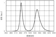
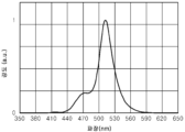
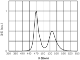
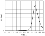
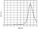
- 6A to 6O are graphs showing emission spectra of light emitting devices manufactured according to various embodiments.
- FIG. 6A is a graph showing a spectrum of light having a plurality of peaks and having CIE coordinates (x,y) within the range of 0.2 ⁇ x ⁇ 0.48 and 0.15 ⁇ y ⁇ 0.4.
- FIG. 6B is a graph showing a spectrum of light having a single peak and CIE coordinates (x, y) within the ranges of 0.17 ⁇ x ⁇ 0.38 and 0.4 ⁇ Y ⁇ 0.8.
- 6C is a graph showing a spectrum of light having a plurality of peaks and having CIE coordinates (x,y) within the range of 0 ⁇ x ⁇ 0.3 and 0.35 ⁇ Y ⁇ 0.85.
- 6D is a graph showing a spectrum of light having a plurality of peaks and having CIE coordinates (x,y) within the range of 0.03 ⁇ x ⁇ 0.25 and 0.25 ⁇ Y ⁇ 0.35.
- 6E is a graph showing a spectrum of light having a plurality of peaks and having CIE coordinates (x,y) within the range of 0.02 ⁇ x ⁇ 0.25 and 0.35 ⁇ Y ⁇ 0.48.
- FIG. 6F is a graph showing a spectrum of light having a plurality of peaks and having CIE coordinates (x,y) within the range of 0.13 ⁇ x ⁇ 0.22 and 0 ⁇ Y ⁇ 0.2.
- 6G is a graph showing a spectrum of light having a plurality of peaks and having CIE coordinates (x,y) within the ranges of 0.35 ⁇ x ⁇ 0.45 and 0.43 ⁇ Y ⁇ 0.62.
- 6H is a graph showing a spectrum of light having a plurality of peaks and CIE coordinates (x,y) within the range of 0.17 ⁇ x ⁇ 0.25 and 0 ⁇ Y ⁇ 0.2.
- 6I is a graph showing a spectrum of light having a single peak and CIE coordinates (x,y) within the range of 0.39 ⁇ x ⁇ 0.49 and 0.45 ⁇ Y ⁇ 0.55.
- 6J is a graph showing a spectrum of light having a plurality of peaks and having CIE coordinates (x,y) within the ranges of 0.44 ⁇ x ⁇ 0.53 and 0.45 ⁇ Y ⁇ 0.52.
- 6K is a graph showing a spectrum of light having a plurality of peaks and having CIE coordinates (x,y) within the ranges of 0.2 ⁇ x ⁇ 0.33 and 0.02 ⁇ Y ⁇ 0.22.
- 6L is a graph showing a light spectrum in which the light emitting device has a single peak and CIE coordinates (x,y) are within the ranges of 0.46 ⁇ x ⁇ 0.55 and 0.43 ⁇ Y ⁇ 0.49.
- 6M is a graph showing a spectrum of light having a plurality of peaks in a light emitting device and having CIE coordinates (x,y) within the range of 0.28 ⁇ x ⁇ 0.38 and 0.06 ⁇ Y ⁇ 0.24.
- 6N is a graph showing a spectrum of light having a plurality of peaks in a light emitting device and having CIE coordinates (x,y) within the range of 0.28 ⁇ x ⁇ 0.38 and 0.06 ⁇ Y ⁇ 0.24.
- 60 is a graph showing a spectrum of light having a plurality of peaks and having CIE coordinates (x,y) within the ranges of 0.36 ⁇ x ⁇ 0.55 and 0.25 ⁇ Y ⁇ 0.35.
- FIG. 7A and 7B are schematic cross-sectional views illustrating a method of manufacturing a light emitting device according to an embodiment of the present disclosure.
- FIG. 7A shows a step in which a first stress relieving layer is formed on the lower surface of the substrate.
- FIG. 7B illustrates steps in forming a light emitting structure to the structure of FIG. 7A.
- FIGS. 8A to 8D are schematic cross-sectional views illustrating a method of manufacturing a light emitting device according to an embodiment of the present disclosure.
- FIG. 8A illustrates forming an ohmic electrode and first and second contact electrodes on a light emitting structure.
- Figure 8B shows the structure of Figure 8A where the first stress relieving layer and a portion of the substrate are removed.
- FIG. 8C shows a step of dividing the substrate through a dicing (D) process after the step of FIG. 8B.
- Fig. 8D shows a step of providing a light emitting device that has gone through the dividing step shown in Fig. 8C.
- FIG. 9 is a schematic cross-sectional view for explaining an example applied to a light emitting device package according to an embodiment of the present disclosure.
- 10A to 10D are schematic cross-sectional views for explaining a method of manufacturing a light emitting device according to another embodiment of the present disclosure.
- 10A shows a step of removing the first stress relieving layer by grinding the lower surface of the substrate on which the first stress relieving layer is grown.
- 10B shows a step of forming a second insulating reflective layer on the lower portion of the substrate.
- 10C shows the step of dividing through a dicing (D) process.
- Fig. 10D shows a step of providing a light emitting device that has gone through the dividing step shown in Fig. 10C.
- 11A is a schematic cross-sectional view for explaining an example applied to a light emitting device package according to another embodiment of the present disclosure.
- 11B is a schematic cross-sectional view for explaining an example applied to a light emitting device package according to another embodiment of the present disclosure.
- 12A to 12D are schematic cross-sectional views for explaining a method of manufacturing a light emitting device according to another embodiment of the present disclosure.
- FIG. 12A shows steps of forming a substrate, a first stress relieving layer, a second stress relieving layer, and a light emitting structure.
- FIG. 12B illustrates a step of removing the first stress relieving layer by grinding the lower surface of the substrate on which the first stress relieving layer is grown, and removing at least a portion of the substrate.
- Fig. 12D shows a step of providing a light emitting device that has gone through the dividing step shown in Fig. 12C.
- FIG. 13 is a schematic cross-sectional view for explaining an example applied to a light emitting device package according to another embodiment of the present disclosure.
- 14A to 14D are schematic cross-sectional views for explaining a method of manufacturing a light emitting device according to another embodiment of the present disclosure.
- FIG. 14A shows steps of forming a substrate, a first stress relieving layer, a second stress relieving layer, and a light emitting structure.
- FIG. 14B illustrates a step of removing the first stress relieving layer by grinding the lower surface of the substrate on which the first stress relieving layer is grown, and removing at least a portion of the substrate.
- 14C shows the step of dividing through a dicing (D) process.
- Fig. 14D shows a step of providing a light emitting device that has gone through the dividing step shown in Fig. 14C.
- 15A and 15B are schematic cross-sectional views for explaining an example applied to a light emitting device package according to another embodiment of the present disclosure.
- 15A shows a step in which a light emitting element is disposed on an electrode located on an upper surface of a circuit board and a molding layer is formed.
- 15B shows a step of forming a dome-shaped lens structure in which the upper surface of the molding layer is convex.
- 16A and 16B are schematic cross-sectional views illustrating a method of manufacturing a light emitting device according to another embodiment of the present disclosure.
- 16A illustrates the formation of a first stress relieving layer on the lower surface of the substrate.
- FIG. 16B illustrates the steps of forming a light emitting structure in the structure of FIG. 16A.
- 17A is a schematic cross-sectional view for explaining an example of application to a unit pixel according to another embodiment of the present disclosure.
- Fig. 17B is a schematic cross-sectional view taken along the line A-A' in Fig. 17A.
- FIG. 18 is a schematic cross-sectional view for explaining an example applied to a display device according to another embodiment of the present disclosure.
- 19A is a schematic plan view for explaining a light emitting module according to an embodiment of the present disclosure.
- Fig. 19B is a schematic cross-sectional view taken along the line B-B' in Fig. 19A.
- 20 is a schematic cross-sectional view for explaining a light emitting module according to an embodiment of the present disclosure.
- 21 is a schematic perspective view for explaining a lighting device according to an embodiment of the present disclosure.
- FIG. 1 is a cross-sectional view of a light emitting module according to a first embodiment.
- the light emitting module includes a substrate 100 and a plurality of light source units arranged on the substrate 100 .
- the substrate 100 is not particularly limited, and may have various forms such as a printed circuit board, a transparent substrate, a flexible substrate, a polyimide substrate, a graphene substrate, and an optical fiber.
- the substrate 100 may have a circuit pattern electrically connected to the light emitting devices 101 , 102 , and 103 .
- the first light source unit includes a light emitting element 101 and a wavelength converter 101a
- the second light source unit includes a light emitting element 102 and a wavelength converter 102a
- the third light emitting unit 103 includes a light emitting element (103).
- the light source unit includes a light emitting element or a combination of a light emitting element and a wavelength converter.
- the first to third light source units may emit light of different colors.
- the light emitting devices 101 , 102 , and 103 may be horizontal light emitting diode chips and may be electrically connected to the circuit pattern of the substrate 100 through bonding wires 104 .
- the light emitting elements 101, 102, and 103 may emit light having peak wavelengths similar to each other, but are not limited thereto, and may emit light having peak wavelengths of different colors.
- wavelength converters 101a and 102a are disposed on at least some of the light emitting devices 101 , 102 , and 103 .
- wavelength converters 101a and 102a emitting light of different colors may be disposed on the light emitting element 101 and the light emitting element 102, and the wavelength converter may not be disposed on the light emitting element 103. there is.
- the wavelength converters 101a and 101b convert the light emitted from the light emitting elements 101 and 102 into light of different wavelengths, respectively.
- the wavelength converters 101a and 101b may include phosphors or quantum dots.
- the light emitting module according to the present embodiment may implement light of various colors by using the light emitting devices 101, 102, and 103 and the wavelength converters 101a and 102a.
- FIG. 2 is a cross-sectional view of a light emitting module according to a second embodiment.
- the light emitting module includes a substrate 200 and a plurality of light emitting units arranged on the substrate 200, and further includes a control unit 204 and a protective material 205. can do.
- the light emitting units may include a combination of light emitting elements 201 , 202 , and 203 and wavelength converters 201a and 202a.
- the substrate 200 is similar to the substrate 100 described with reference to FIG. 1 , and detailed descriptions of the substrate 100 may be referred to in relation to the substrate 200 .
- the light emitting devices 201 , 202 , and 203 may be mounted on the substrate 200 using electrode pads instead of bonding wires.
- the light emitting elements 201 , 202 , and 203 may have electrode pads facing the substrate 200 , and the electrode pads may be bonded to the pads on the substrate 200 .
- the light emitting elements 201, 202, and 203 may be flip chip type light emitting diode chips.
- the wavelength converters 201a and 202a can be uniformly formed on the upper surfaces of the light emitting devices 201 and 202, and can be applied to substrates whose shape is deformed, such as a flexible substrate or a polyimide substrate. In this case, the short circuit of the electrode can be minimized.
- the light emitting devices 201 , 202 , and 203 may be connected in series using a circuit on the board 100 to be driven together, or may be connected to a circuit on the board 100 to enable individual driving. When electrically connected so that individual driving is possible, even if one light emitting element is short-circuited and driving failure occurs, the other light emitting element can be driven so that the driving of the light emitting module can be maintained.
- the light emitting elements 201, 202, and 203 may emit light having peak wavelengths similar to each other, but are not limited thereto, and may emit light having peak wavelengths of different colors.
- wavelength converters 201a and 202a may be disposed on at least some of the light emitting elements 201 , 202 , and 203 .
- wavelength converters 201a and 202a emitting light of different colors are disposed on the light emitting element 201 and the light emitting element 202, respectively, and the light emitting element 203 A wavelength converter may not be disposed on the top.
- the wavelength converters 201a and 202a convert the light emitted from the light emitting elements 201 and 202 into light of different wavelengths, respectively.
- the wavelength converters 201a and 202a may include phosphors or quantum dots.
- the light emitting devices 201, 202, and 203 may emit light in the ultraviolet or visible ray region, and the wavelength converters 201a and 202a may include phosphors or quantum dots having high color temperature stability. . Wavelength converters 201a and 202a may also be used to achieve a high color rendering index (CRI).
- CRI color rendering index
- the wavelength converters 101a and 201a may include a red light emitting phosphor.
- the red light-emitting phosphor may be, for example, a Mn(IV)-activated light-emitting material based on an oxidohalide host lattice represented by the following general formula 1:
- Red-emitting fluorescent materials with emission maxima in the range between 610 and 640 nm, high quantum efficiency, long lifetime and high color temperature stability have the general formula (A 4-a B a ) m/2+n/ It can be implemented by incorporating Mn(IV) ions into an oxidohalide host lattice of general formula (I) to obtain a compound of 2 X 2m [MX 4 O 2 ] n :Mn(IV).
- the fluorescent material can be obtained efficiently and inexpensively through simple synthesis.
- Cr(VI), Mo(VI), W(VI) and/or Re(VI) are used for fluoride compounds with long-term stability, the corresponding octahedral oxidos of the general form [MX 4 O 2 ] 2- This is because halide complex anions have very high stability.
- halide complex anions have very high stability.
- oxidohalides have greater stability due to their higher lattice energy compared to fluorides.
- significant ⁇ back-bonding reduces the effective ionic charge density of halide and W(VI) ions.
- the phosphor is a red-emitting Mn(IV) luminescent material, and may have multiple peaks in the red spectral region, and has a maximum peak value in a range between 610 and 640 nm, particularly between 620 and 635 nm.
- Preferred alkyl radicals in the above general formula (I) are linear C1-C5-alkyl radicals or branched C3-C5-alkyl radicals. Particularly preferred alkyl radicals are methyl, ethyl, propyl, butyl and pentyl. Also preferred aryl radicals are phenyl, naphthyl, anthryl and phenanthryl, which are methyl, ethyl, propyl, butyl, methoxy, ethoxy, hydroxy optionally substituted by one or more radicals selected from oxyl, fluoride, chloride and trifluoromethyl.
- A is a single charged hydrogen and/or deuterium cation A +
- B is a single charged metal and/or ammonium cation B +
- M is a hexavalent charged metal atom M 6+
- Mn(IV) exists as a tetravalent charged metal atom Mn 4+
- halogen X exists as a halide (X ⁇ )
- oxygen (O) as an oxide (O 2 ⁇ ).
- the Mn(IV)-activated luminescent material of the present invention is a conversion material doped with Mn 4+ , wherein one Mn 4+ ion and two X ⁇ ions generate one M 6+ ion and two O 2 ⁇ ions. replace Thus, the charge is balanced by the additional incorporation of two X - ions and the absence of two O 2- ions.
- the compounds of the present invention are generally capable of being excited by light in the spectral region of about 250 to about 550 nm, preferably about 325 to about 525 nm, wherein the absorption maximum is 425 to 500 nm, and typically about 600 to about 525 nm. It emits in the red spectral region of 650 nm, where the emission maximum is in the region between 610 and 640 nm, preferably between 620 and 635 nm.
- the compounds of the present invention also exhibit high photoluminescence quantum yields, and have high spectral purity and high color temperature stability when used in LEDs.
- ultraviolet light refers to light having emission maxima between 100 nm and 399 nm
- violet light refers to light having emission maxima between 400 nm and 430 nm
- blue light refers to light having emission maxima between 431 and 480 nm.
- cyan light represents light with emission maxima between 481 and 510 nm
- green light represents light with emission maxima between 511 and 565 nm
- yellow light represents light with emission maxima between 566 and 575 nm
- Orange light represents light with emission maxima between 576 and 600 nm
- red light represents light with emission maxima between 601 and 750 nm.
- Mn(IV)-doped compound of formula (I) is represented by formula (II):
- A is selected from the group consisting of H and D and mixtures thereof, wherein D is deuterium;
- B is selected from the group consisting of Li, Na, K, Rb, Cs, NH4, ND4, NR4 and mixtures of two or more thereof, wherein R is an alkyl or aryl radical;
- X is selected from the group consisting of F and Cl and mixtures thereof;
- M is selected from the group consisting of Cr, Mo, W, Re and mixtures of two or more thereof; and 0 ⁇ a ⁇ 4; 0 ⁇ m ⁇ 10; 1 ⁇ n ⁇ 10; and 0 ⁇ x ⁇ 1.0.
- a of general formulas (I) and (II) preferably 1 ⁇ a ⁇ 4, more preferably 2.0 ⁇ a ⁇ 4.0.
- a in formulas (I) and (II) is an integer from 1 to 4, more preferably an integer selected from 2, 3 and 4. Most preferably, a in formulas (I) and (II) is 3.0.
- m in formulas (I) and (II) preferably 0.1 ⁇ m ⁇ 5, more preferably 0.5 ⁇ m ⁇ 3.0, most preferably 0.75 ⁇ m ⁇ 1.50.
- m in formulas (I) and (II) is an integer selected from 1, 2 and 3. Most preferably, m in formulas (I) and (II) is 1.0.
- n of general formulas (I) and (II) preferably 1 ⁇ n ⁇ 5, more preferably 1.0 ⁇ n ⁇ 3.0.
- n in formulas (I) and (II) is an integer from 1 to 5, more preferably an integer selected from 1, 2 and 3.
- n in formulas (I) and (II) is 1.0.
- Mn(IV)-doped compound of general formula (I) or the compound of general formula (II) is represented by general formula (III):
- Formula (III) AB 3 M 1-x X 6+2x O 2-2x :Mn(IV) x , where A, B, X and M are one of the definitions given above for formula (I) and/or formula (II) and x is: 0 ⁇ x ⁇ 1.0.
- a in formulas (I), (II) and/or (III) is H or D, wherein D is deuterium; More preferably A is H.
- B in formulas (I), (II) and/or (III) is selected from the group consisting of Na, K, Cs and mixtures of two or three thereof; More preferably A is selected from the group consisting of Na and K.
- X in formulas (I), (II) and/or (III) is F, wherein optionally at most 10 atomic % of X is Cl, more preferably at most 5 atomic %. More preferably, X in formulas (I), (II) and/or (III) is F.
- M in formulas (I), (II) and/or (III) is selected from the group consisting of Mo, W and mixtures of Mo and W, wherein Cr and/or Re may optionally be present.
- M in formulas (I), (II) and/or (III) is Cr and Mo; Mo and W; Cr and W; Cr and Re; Mo and Re; W and Re; Cr, Mo and W; Cr, Mo and Re; Cr, W and Re; Mo, W and Re; and mixtures consisting of Cr, Mo, W and Re.
- the exponent x of formulas (II) and (III) is: 0 ⁇ x ⁇ 0.80, more preferably 0 ⁇ x ⁇ 0.60, more preferably 0.0001 ⁇ x ⁇ 0.40, particularly preferred preferably 0.001 ⁇ x ⁇ 0.20, more particularly preferably 0.001 ⁇ x ⁇ 0.10 and most preferably 0.002 ⁇ x ⁇ 0.05.
- A is selected from the group consisting of H and D and mixtures thereof, wherein D is deuterium; B is selected from the group consisting of Na, K, Rb and mixtures of two or three of them; X is F; M is selected from the group consisting of Mo, W and mixtures of Mo and W, wherein Cr and/or Re may optionally be present; 0.0001 ⁇ x ⁇ 0.40, more preferably 0.001 ⁇ x ⁇ 0.20, particularly preferably 0.001 ⁇ x ⁇ 0.10, most preferably 0.002 ⁇ x ⁇ 0.05.
- the wavelength converters 102a and 202a may include, for example, green or yellow phosphors.
- phosphors that emit light in the green wavelength band include yttrium-aluminum-garnet-based phosphors (eg Y 3 (Al,Ga) 5 O 12 :Ce), lutetium-aluminum-garnet-based phosphors (eg Lu 3 (Al, Ga) 5 O 12 :Ce), terbium/aluminum/garnet-based phosphors (e.g. Tb 3 (Al, Ga) 5 O 12 :Ce), silicate-based phosphors (e.g.
- the yttrium ⁇ aluminum ⁇ garnet-based phosphor can shift the emission peak wavelength toward a longer wavelength by substituting a part of Y with Gd, thereby enabling emission in a yellow wavelength region.
- the light emitting devices 101, 102, and 103; 201, 202, and 203 described with reference to FIGS. 1 and 2 may be independently controlled and driven.
- the light emitting module may further include a control unit 204 as shown in FIG. 2 .
- the control unit 204 may be disposed on the substrate 200 .
- the control unit 204 may implement a light emitting pattern or light emitting wavelength according to a user's input. For example, all light emitting elements mounted on the substrate 200 may be driven, or, on the other hand, only some light emitting elements may be driven, through which light of a light emitting pattern or light emitting wavelength desired by a user may be implemented. there is. Accordingly, the light emitting module may be used for emotional lighting devices indoors or outdoors of a building or interior or exterior of a vehicle.
- a protective material 205 covers the light emitting devices 201 , 202 , and 203 .
- the protective material 205 may prevent the light emitting devices 201 , 202 , and 203 from being separated from the substrate 200 .
- the protective material 205 adheres the light emitting elements 201 , 202 , and 203 to the substrate 200 to prevent peeling.
- the protective material 205 protects the light emitting elements 201, 202, and 203 from the external environment.
- the protective material 205 may have a curved shape, and by using the curved shape, light emission efficiency may be increased like a lens.
- protective material 205 may be formed of transparent silicon.
- protective material 205 may also include a light diffusing material.
- the light diffusing material diffuses light generated from the light emitting elements 201, 202, and 203 over a wide area. Therefore, for example, even if only some of the light emitting devices 201 , 202 , and 203 mounted on the substrate 200 are turned on, the light may spread widely to the surroundings through the light diffusing material 205 . Accordingly, it is possible to remove a dark portion that may occur in a defective light emitting element or a region between light emitting elements, and implement a linear or planar light source.
- the light emitted from the light emitting elements can be mixed with each other by the light diffusing material in the protective material 205, and through this, a small number of light emitting elements It is possible to implement light of various colors by using.
- some light source units include wavelength converters 101a and 102a; 201a and 202a to describe a light emitting module that implements light of various colors, but the light source units A light emitting module that implements light of various colors without a wavelength converter may be provided.
- a light emitting module that implements light of various colors using light emitting elements without a wavelength converter will be described.
- 3 is a cross-sectional view of a light emitting module according to a third embodiment
- FIG. 4 is a cross-sectional view illustrating a light emitting device according to a fourth embodiment
- FIG. 5 is a partially enlarged cross-sectional view of FIG. 4 .
- the light emitting module includes a substrate 300 and light emitting elements 301 , and may further include a control unit 304 and a protective material 305 .
- each light source unit implements color using the light emitting element 301 without a wavelength converter.
- the substrate 300, the control unit 304, and the protective material 305 are similar to the substrate 200, the control unit 204, and the protective material 205 described above, and detailed descriptions are omitted.
- the light emitting elements 301 include light emitting elements exhibiting different light emitting spectra.
- the light emitting elements 301 (C1 to Cn) include at least one light emitting element to be described later with reference to FIG. 4 .
- the light emitting device 301 includes a substrate 400, a first conductive semiconductor layer 401, a lower multi-quantum well structure 402, an upper multi-quantum well structure 403, a second A conductive semiconductor layer 404, a spacer layer 405, and a step coverage layer 403s may be included.
- the light emitting element 301 includes an electrical connection structure to be electrically connected to the circuit pattern of the substrate 300 .
- the light emitting element 301 may include an ohmic layer making ohmic contact with the first and second conductivity type semiconductor layers 401 and 404 and electrode pads.
- the substrate 400 may be a growth substrate for growing a gallium nitride-based semiconductor layer, such as a sapphire substrate, a silicon substrate, a SiC substrate, a spinel substrate, and the like.
- the substrate 400 may be a patterned sapphire substrate.
- the first conductivity-type semiconductor layer 401 may be multi-layered and may include, for example, a nuclear layer, a high-temperature buffer layer, and an n-type impurity doped layer. Also, the first conductivity type semiconductor layer 401 may include a plurality of grooves on an upper surface.
- the semiconductor layer formed on the first conductive semiconductor layer 401 may be formed of, for example, a GaN layer, and a plurality of grooves may be formed by growing the GaN layer at a temperature of about 900° C. or less.
- the second conductivity type semiconductor layer 404 is disposed on the first conductivity type semiconductor layer 401 .
- the second conductivity-type semiconductor layer 404 may be formed as a single layer or multiple layers, and may include, for example, a layer doped with p-type impurities.
- a lower multiple quantum well structure 402 and an upper multiple quantum well structure 403 are disposed between the first conductivity type semiconductor layer 402 and the second conductivity type semiconductor layer 404, and the lower multiple quantum well structure 402
- a spacing layer 405 may be disposed between the and the upper multi-quantum well structure 404 .
- the lower multi-quantum well structure 402 may be formed on the first conductivity type semiconductor layer 401 .
- the lower multi-quantum well structure 402 has a structure in which barrier layers 402b and well layers 402w are alternately stacked.
- the well layer 402w has a composition for emitting light of the first wavelength.
- the well layer 402w may be formed of an InGaN layer or an AlInGaN layer, and may emit light in an ultraviolet, blue, or green region.
- the content of In included in the well layer 402w may be 18 atom % or less, and furthermore, 12 atom % or less with respect to all Group 3 elements.
- the upper multi-quantum well structure 403 is disposed on the lower multi-quantum well structure 402, and has a structure in which a barrier layer 403b and a well layer 403w are alternately stacked.
- the well layer 403w has a composition for emitting light of the second wavelength.
- the light of the second wavelength may have a longer wavelength than the light of the first wavelength.
- the well layer 403w may be formed of an InGaN layer or an AlInGaN layer, and may emit light in a green or red region.
- the content of In included in the well layer 403w may be 15 atomic % or more and less than 30 atomic % with respect to all Group 3 elements.
- the barrier layers 403b in the upper multi-quantum well structure 403 may be thicker than the barrier layers 402b in the lower multi-quantum well structure 402 .
- the well layers 403w in the upper multi-quantum well structure 403 may be thicker than the well layers 402w in the lower multi-quantum well structure 402 .
- the barrier layers 403b may be formed relatively thick to prevent electrons and holes from overflowing.
- the thickness of the barrier layers 402b is adjusted so that holes are well dispersed in the lower multi-quantum well structure 402. can be made relatively thin.
- the barrier layers 402b may have a thickness of 4 nm to 7 nm, and the barrier layers 403b may have a thickness of 8 nm to 15 nm.
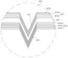
- the upper multi-quantum well structure 403 may include a first region R1 and a second region R2.
- the first region R1 may have a substantially flat surface, and the second region R2 may have a non-planar surface.
- the second region R2 forms a groove as the non-planar surface.
- the grooves may be formed to have a V-shape, but the present disclosure is not limited thereto.
- the first region R1 is formed of a plurality of regions in the cross-sectional view of FIG. 4 . In a plan view, the first region R1 surrounds the plurality of second regions R2.
- the second regions R2 may be disposed on grooves formed on the first conductive semiconductor layer 401 .
- the barrier layers 403b and the well layers 403w of the upper multi-quantum well structure 403 are continuously disposed in the first region R1 and the second region R2. Top surfaces of the barrier layers 403b and the well layers 403w may have a curved shape at a position where the first region R1 and the second region R2 meet. Accordingly, it is possible to prevent cracks from occurring in the barrier layers 403b or the well layers 403w, thereby preventing charge leakage.
- the barrier layers 403b and the well layers 403w have different thicknesses in the first region R1 and the second region R2. That is, the thicknesses of the barrier layers 403b and the well layers 403w in the first region R1 are greater than the thicknesses of the barrier layers 403b and the well layers 403w in the second region R2. can be formed Furthermore, the In content in the well layers 403w of the second region R2 is less than the In content of the well layers 403w in the first region R1. Accordingly, the multi-quantum well structure 403 includes a multi-quantum well structure in the first region R1 and a multi-quantum well structure 407 in the second region, which are different from each other.
- the multi-quantum well structure 407 of the second region R2 has a shorter wavelength than the light of the second wavelength. It can emit light of 3 wavelengths. Additionally or alternatively, the light of the third wavelength may have a shorter wavelength, a longer wavelength, or the same wavelength as the light of the first wavelength emitted from the lower multi-quantum well structure 402 .
- the content of In in the well layers 403w in the first region R1 may be greater than or equal to 15 atomic% and less than 30 atomic% with respect to all Group III elements to emit light of the first wavelength.
- the content of In in the well layers 403w in the second region R2 is about 7 to less than about 12 atomic%, furthermore, about 8 to about less than about 8 to about It may be 10 atomic %.
- the width D4 of the first region R1 may be greater than the width D2 of the second region R2, and thus, the second conductive layer formed on the upper multi-quantum well structure 403.
- a relatively wide flat surface can be formed on the type semiconductor layer 404 , and an electrode can be easily formed on the second conductivity type semiconductor layer 404 .
- the lower multi-quantum well structure 402 may also include a third region R3 having a flat surface and a fourth region R4 having a non-planar surface forming a groove. Thicknesses of the barrier layers 402b and the well layers 402w in the third region R3 may be greater than those of the barrier layers 402b and the well layers 402w in the fourth region R4 .
- the fourth regions R4 are positioned below the second regions R2. As shown in FIG. 4 , at least a portion of the groove of the second region R2 and the groove of the fourth region R4 may overlap in a vertical direction. Also, a portion of the second region R2 closest to the substrate 400 may be positioned within the groove region of the fourth region R4 .
- the lower multi-quantum well structure 402 may emit light of the first wavelength described above in the third region R3, and the multi-quantum well structure 406 in the fourth region R4 may not emit light.
- the present disclosure is not limited thereto, and the multi-quantum well structure 406 in the fourth region R4 may emit light having a shorter wavelength than light having a first wavelength.
- the number of pairs of layers constituting the lower multiquantum well structure 402 affects the peak intensity of light of the first wavelength. As the number of pairs of the lower multi-quantum well structure 402 increases, the peak intensity of light of the first wavelength, for example, the blue region may increase. Also, the number of pairs of the lower multi-quantum well structure 402 and the number of pairs of the upper multi-quantum well structure 403 may be adjusted to be different from each other. For example, the number of pairs of the lower multi-quantum well structure 402 may be greater than the number of pairs of the upper multi-quantum well structure 403, and thus, the peak intensity of the light of the first wavelength is greater than the peak intensity of the light of the second wavelength.
- the well layers of the lower multi-quantum well structure 402 may have different band gaps.
- the lower multi-quantum well structure 402 may include a first group of well layers and a second group of well layers, and the first group of well layers are relatively smaller than the second group of well layers. It may have a high In content.
- the well layers of the second group may be disposed between the well layers of the first group and the upper multiquantum well structure 403 .
- the well layers of the first group may include an In content of 10 atomic % or more, and the well layers of the second group may include an In content of less than 10 atomic %.
- the number of pairs of the lower multi-quantum well structure 402 may be smaller than the number of pairs of the upper multi-quantum well structure 403 . Accordingly, in the spectrum of light emitted from the light emitting device 301, the peak intensity of the short wavelength region may be smaller than the peak intensity of the long wavelength region.
- the spacing layer 405 may be disposed between the lower multi-quantum well structure 402 and the upper multi-quantum well structure 403 .
- the spacing layer 405 may have a band gap equal to or wider than that of the barrier layer 402b in the lower multi-quantum well structure 402 .
- the spacing layer 405 may include GaN, AlGaN, or AlInGaN.
- the spacing layer 405 when the spacing layer 405 includes a relatively high Al content and has a wide band gap, the spacing layer 405 prevents holes from being injected into the lower multiquantum well structure 402 . Accordingly, the number of electron-hole pairs in the lower multi-quantum well structure 402 decreases, and thus the light emission intensity decreases. Conversely, the number of holes trapped in the upper multi-quantum well structure 403 increases, and thus the luminous intensity of the upper multi-quantum well structure 403 increases. The thickness of the spacing layer 405 also affects hole injection.
- the lower multiple quantum well 402 and the upper multiple quantum well structure 402 and the upper multiple quantum well structure 405 are formed.
- the relative luminous intensity of the well structure 403 can be adjusted.
- a step coverage layer 403s is disposed on the upper multiquantum well structure 403 .
- the step coverage layer 403s may have a wider bandgap than the barrier layer 403b of the upper multi-quantum well structure 403 .
- the step coverage layer 403s may be formed of AlGaN or AlInGaN, for example.
- the step coverage layer 403s may be an Al grading layer whose Al content decreases as the distance from the upper multi-quantum well structure 403 increases.
- the Al content in the step coverage layer 403s may decrease in the thickness direction from 30 atomic % or more to 10 atomic % or less.
- the thickness of the step coverage layer 403s may be less than about 100 nm, and in certain embodiments may be less than about 50 nm, and even less than about 30 nm.
- the step coverage layer 403s By forming the step coverage layer 403s as a grading layer, holes can be smoothly injected into the upper multi-quantum well structure 403, and in the second region R2 of the upper multi-quantum well structure 403, It can help generate light of 3 wavelengths.
- the intensity of light having a peak wavelength of a long wavelength may be controlled to be superior to light having a peak wavelength of a short wavelength emitted through the electroluminescence through the step coverage layer 403s.
- the second conductivity type semiconductor layer 404 may be disposed on the step coverage layer 403s.
- the second conductive semiconductor layer 404 may include surface grooves 408 corresponding to the second regions R2 .
- the entrance width of the surface groove 408 may be greater than the entrance width of the grooves of the second regions R2 .
- the sub-surface groove 409 may be formed on the upper portion of the first region R1 , and the entrance width of the sub-surface groove 409 may be smaller than the entrance width of the surface groove 408 .
- Light extraction efficiency may be improved by varying the size of the surface grooves 408 and 409 .
- the surface grooves 408 and 409 may increase a contact area of an ohmic electrode such as ITO to lower a driving voltage and improve reliability of the light emitting element 301 .
- a lower multi-quantum well structure 402 and an upper multi-quantum well structure 403 are disposed, and the number of pairs of barrier layers and well layers in these multi-quantum well structures 402 and 403, the well layer
- light of a wavelength for sterilization desired by the user can be implemented from the light emitting element 301, and the sterilization wavelength can be controlled.
- 6A to 6O show emission spectra of various light emitting devices 301 obtained by adjusting the lower and upper multi-quantum well structures 402 and 403, the step coverage layer 403s, and the spacing layer 405.
- the light emitting element 301 was driven under a current density of about 35 A/cm 2 .
- a single peak or a plurality of peaks can be generated in one light emitting device.
- Light having a peak may be emitted.
- active layers emitting light having a plurality of peaks for example, the lower quantum well structure 402 and the upper quantum well structure 403 are formed by the first conductivity type semiconductor layer 402 or the second conductivity type semiconductor layer 402 .
- the conductive semiconductor layer 404 is shared, or the substrate 400 is shared.
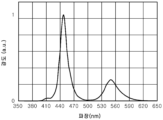
- the light emitting device may emit light having a plurality of peaks and having CIE coordinates (x,y) within a range of 0.2 ⁇ x ⁇ 0.48 and 0.15 ⁇ y ⁇ 0.4.
- the color coordinates of light emitted from the light emitting device of this embodiment are approximately (0.21, 0.27).
- the light emitting device may emit light close to white without a phosphor.
- the plurality of peaks may include a first peak within a range of 400 to 500 nm and a second peak within a range of 500 to 600 nm, and a short-wavelength peak may exhibit higher intensity than a long-wavelength peak.
- the light emitting device may emit light having a single peak and having CIE coordinates (x,y) within the ranges of 0.17 ⁇ x ⁇ 0.38 and 0.4 ⁇ Y ⁇ 0.8.
- the color coordinates of emitted light are approximately (0.27, 0.70).
- the light emitting device may emit yellowish green light without a phosphor through light of a second wavelength emitted from the first region of the upper quantum well structure 403 .
- the light emitting device may emit light having a plurality of peaks and having CIE coordinates (x,y) within a range of 0 ⁇ x ⁇ 0.3 and 0.35 ⁇ Y ⁇ 0.85.
- the color coordinates of emitted light are approximately (0.15, 0.64).
- the light emitting element may emit green light without a phosphor.
- the plurality of peaks may include a first peak in a range of 400 to 500 nm and a second peak in a range of 500 to 600 nm, and a short wavelength peak may exhibit a smaller emission intensity than a long wavelength peak.
- the light emitting device may emit light having a plurality of peaks and having CIE coordinates (x,y) within the ranges of 0.03 ⁇ x ⁇ 0.25 and 0.25 ⁇ Y ⁇ 0.35.
- the color coordinates of emitted light are approximately (0.19, 0.33).
- the light emitting device may emit blue green light without a phosphor.
- the plurality of peaks include a first peak within a range of 400 to 500 nm and a second peak within a range of 500 to 600 nm, and a short-wavelength peak within a range of 400-500 nm may exhibit a higher emission intensity than a long-wavelength peak within a range of 500-600 nm. .
- the light emitting device may emit light having a plurality of peaks and having CIE coordinates (x,y) within a range of 0.02 ⁇ x ⁇ 0.25 and 0.35 ⁇ Y ⁇ 0.48.
- the color coordinates of emitted light are approximately (0.21, 0.38).
- the light emitting device may emit bluish green light without a phosphor.
- the plurality of peaks include a first peak within a range of 400 to 500 nm and a second peak within a range of 500 to 600 nm, and a short-wavelength peak within a range of 400-500 nm may exhibit a higher emission intensity than a long-wavelength peak within a range of 500-600 nm. .
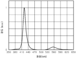
- the light emitting device may emit light having a plurality of peaks and having CIE coordinates (x,y) within a range of 0.13 ⁇ x ⁇ 0.22 and 0 ⁇ y ⁇ 0.2.
- the color coordinates of emitted light are approximately (0.20, 0.17).
- the light emitting device may emit purple blue light without a phosphor.
- the plurality of peaks include a first peak within a range of 400 to 500 nm and a second peak within a range of 500 to 600 nm, and a short-wavelength peak within a range of 400-500 nm may exhibit a higher emission intensity than a long-wavelength peak within a range of 500-600 nm. .
- the light emitting device may emit light having a plurality of peaks and having CIE coordinates (x,y) within a range of 0.35 ⁇ x ⁇ 0.45 and 0.43 ⁇ Y ⁇ 0.62.
- the color coordinates of emitted light are approximately (0.39, 0.57).
- the light emitting device may emit yellow green light without a phosphor.
- the plurality of peaks include a first peak within a range of 380 to 500 nm and a second peak within a range of 500 to 650 nm, and a short wavelength peak within a range of 480 to 500 nm may exhibit lower emission intensity than a long wavelength peak within a range of 500 to 650 nm. .
- the first peak wavelength may be 410 nm or less, may be within a range of 390 nm to 410 nm, and the second peak wavelength may be 530 nm or more.
- the intensity of the first peak may be 5 times or less than the intensity of the second peak, and a sterilization function may be exhibited while emitting yellow-green light with this height difference.
- the light emitting device may perform a sterilization function as well as a function of a light source.
- the active layer emitting light of the peak wavelength for sterilization and the active layer emitting color light may share a first conductivity type semiconductor layer or a second conductivity type semiconductor layer or may share a substrate.
- the substrate may be a growth substrate.
- the refractive index of the well layer generating the first peak may be lower than the refractive index of the well layer generating the second peak.
- the well layer generating the first peak and the well layer generating the second peak may include Group 3 materials (or elements or atoms), and the well layer generating the second peak may include atoms of Group 3 materials.
- An amount of an atom (or element or material) having the largest size (or element or material) may be smaller than an amount of the same material included in the well layer generating the first peak.
- the bandgap energy of the well layer generating the first peak may be greater than the bandgap energy of the well layer generating the second peak.
- a material (or element or atom) having the largest relative atomic mass is a well generating a second peak more than a well layer generating the first peak.
- Layers can contain more.
- a material (or element or atom) having the largest relative atomic mass among Group 3 materials included in the well layer that generates the second peak or an atom (or element or material) among Group 3 materials included in the well layer The largest atom (or element or material) may be indium.
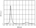
- the light emitting device may emit light having a plurality of peaks and having CIE coordinates (x,y) within the range of 0.17 ⁇ x ⁇ 0.25 and 0 ⁇ Y ⁇ 0.2.
- the color coordinates of emitted light are approximately (0.21, 0.11).
- the light emitting device may emit bluish purple light without a phosphor.
- the plurality of peaks include a first peak in the range of 380 to 500 nm and a second peak in the range of 500 to 650 nm, and the first peak with a short wavelength in the range of 380 to 500 nm has a higher emission intensity than the second peak with a long wavelength in the range of 500 to 650 nm.
- the first peak wavelength may be 425 nm or less, may be in the range of 400 nm to 415 nm, and the second peak wavelength may be 530 nm or more.
- the intensity of the first peak may be 5 times higher than that of the second peak, and the sterilization function may be exhibited while emitting blue-violet light with this height difference.
- the light emitting device may perform a sterilization function as well as a function of a light source.
- the active layer emitting light of the peak wavelength for sterilization and the active layer emitting color light may share a first conductivity type semiconductor layer or a second conductivity type semiconductor layer or may share a substrate.
- the substrate may be a growth substrate.
- the refractive index of the well layer generating the first peak may be lower than the refractive index of the well layer generating the second peak.
- the well layer generating the first peak and the well layer generating the second peak may include Group 3 materials (or elements or atoms), and the well layer generating the second peak may include atoms of Group 3 materials.
- An amount of an atom (or element or material) having the largest size (or element or material) may be smaller than an amount of the same material included in the well layer generating the first peak.
- the bandgap energy of the well layer generating the first peak may be greater than the bandgap energy of the well layer generating the second peak.
- a material (or element or atom) having the largest relative atomic mass is a well generating a second peak more than a well layer generating the first peak.
- Layers can contain more.
- a material (or element or atom) having the largest relative atomic mass among Group 3 materials included in the well layer that generates the second peak or an atom (or element or material) among Group 3 materials included in the well layer The largest atom (or element or material) may be indium.
- the light emitting device may emit light having a single peak and having CIE coordinates (x,y) within the ranges of 0.39 ⁇ x ⁇ 0.49 and 0.45 ⁇ Y ⁇ 0.55.
- the color coordinates of emitted light are approximately (0.47, 0.52).
- the light emitting device may emit greenish yellow light without a phosphor.
- the light emitting device may emit light having a plurality of peaks and having CIE coordinates (x,y) within a range of 0.44 ⁇ x ⁇ 0.53 and 0.45 ⁇ Y ⁇ 0.52.
- the color coordinates of emitted light are approximately (0.49, 0.50).
- the light emitting element may emit yellow light without a phosphor.
- the plurality of peaks include a first peak in the range of 380 to 500 nm and a second peak in the range of 500 to 650 nm, and a short wavelength peak in the range of 380 to 500 nm may exhibit a lower emission intensity than a long wavelength peak in the range of 500 to 650 nm. .
- the light emitting device may emit light having a plurality of peaks and having CIE coordinates (x,y) within a range of 0.2 ⁇ x ⁇ 0.33 and 0.02 ⁇ y ⁇ 0.22.
- the color coordinates of emitted light are approximately (0.27, 0.19).
- the light emitting device may emit purple light without a phosphor.
- the plurality of peaks include a first peak within a range of 350 to 500 nm and a second peak within a range of 500 to 650 nm, and a short-wavelength peak within a range of 350-500 nm may exhibit a higher emission intensity than a long-wavelength peak within a range of 500-650 nm. .
- the first peak wavelength may be 420 nm or less, and may be within a range of 400 nm to 415 nm, and the second peak wavelength may be 530 nm or more.
- the intensity of the first peak may be 1.5 times higher than that of the second peak, and the sterilization function may be exhibited while emitting purple light with this height difference.
- the light emitting device may perform a sterilization function as well as a function of a light source.
- the active layer emitting light of the peak wavelength for sterilization and the active layer emitting color light may share a first conductivity type semiconductor layer or a second conductivity type semiconductor layer or may share a substrate.
- the substrate may be a growth substrate.
- the refractive index of the well layer generating the first peak may be lower than the refractive index of the well layer generating the second peak.
- the well layer generating the first peak and the well layer generating the second peak may include Group 3 materials (or elements or atoms), and the well layer generating the second peak may include atoms of Group 3 materials.
- An amount of an atom (or element or material) having the largest size (or element or material) may be smaller than an amount of the same material included in the well layer generating the first peak.
- the bandgap energy of the well layer generating the first peak may be greater than the bandgap energy of the well layer generating the second peak.
- a material (or element or atom) having the largest relative atomic mass is a well generating a second peak more than a well layer generating the first peak.
- Layers can contain more.
- a material (or element or atom) having the largest relative atomic mass among Group 3 materials included in the well layer that generates the second peak or an atom (or element or material) among Group 3 materials included in the well layer The largest atom (or element or material) may be indium.
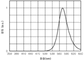
- the light emitting device may emit light having a single peak and having CIE coordinates (x,y) within the ranges of 0.46 ⁇ x ⁇ 0.55 and 0.43 ⁇ y ⁇ 0.49.
- the color coordinates of emitted light are approximately (0.55, 0.44).
- the light emitting device may emit yellowish orange light without a phosphor.
- the single peak may be within a range of 500 to 650 nm.
- the light emitting device may emit light having a plurality of peaks and having CIE coordinates (x,y) within a range of 0.47 ⁇ x ⁇ 0.63 and 0.37 ⁇ y ⁇ 0.45.
- the color coordinates of emitted light are approximately (0.55, 0.43).
- the light emitting device may emit orange light without a phosphor.
- the plurality of peaks include a first peak in the range of 380 to 500 nm and a second peak in the range of 500 to 650 nm, and a short wavelength peak in the range of 380 to 500 nm may exhibit a lower emission intensity than a long wavelength peak in the range of 500 to 650 nm. .
- the light emitting device may emit light having a plurality of peaks and within a range of CIE coordinates (x,y) of 0.28 ⁇ x ⁇ 0.38 and 0.06 ⁇ y ⁇ 0.24.
- the color coordinates of emitted light are approximately (0.32, 0.18).
- the light emitting device may emit reddish purple light without a phosphor.
- the plurality of peaks include a first peak within a range of 350 to 500 nm and a second peak within a range of 500 to 650 nm, and a short-wavelength peak within a range of 350-500 nm may exhibit a higher emission intensity than a long-wavelength peak within a range of 500-650 nm. .
- the first peak wavelength may be 420 nm or less, and may be within a range of 400 nm to 415 nm, and the second peak wavelength may be 550 nm or more.
- the intensity of the first peak may be 10 times higher than that of the second peak, and the sterilization function may be exhibited while emitting reddish purple light with this height difference.
- the light emitting device may perform a sterilization function as well as a function of a light source.
- the active layer emitting light of the peak wavelength for sterilization and the active layer emitting color light may share a first conductivity type semiconductor layer or a second conductivity type semiconductor layer or may share a substrate.
- the substrate may be a growth substrate.
- the refractive index of the well layer generating the first peak may be lower than the refractive index of the well layer generating the second peak.
- the well layer generating the first peak and the well layer generating the second peak may include Group 3 materials (or elements or atoms), and the well layer generating the second peak may include atoms of Group 3 materials.
- An amount of an atom (or element or material) having the largest size (or element or material) may be smaller than an amount of the same material included in the well layer generating the first peak.
- the bandgap energy of the well layer generating the first peak may be greater than the bandgap energy of the well layer generating the second peak.
- a material (or element or atom) having the largest relative atomic mass is a well generating a second peak more than a well layer generating the first peak.
- Layers can contain more.
- a material (or element or atom) having the largest relative atomic mass among Group 3 materials included in the well layer that generates the second peak or an atom (or element or material) among Group 3 materials included in the well layer The largest atom (or element or material) may be indium.
- the light emitting device may emit light having a plurality of peaks and having CIE coordinates (x,y) within a range of 0.36 ⁇ x ⁇ 0.55 and 0.25 ⁇ y ⁇ 0.35.
- the color coordinates of emitted light are approximately (0.41, 0.30).
- the light emitting device may emit pink light without a phosphor.
- the plurality of peaks may include a first peak in a range of 350 to 425 nm and a second peak in a range of 545 to 650 nm, and may include sub-peaks having relatively low emission intensity between the first peak and the second peak.
- the light emitting device may emit light of a second peak wavelength for realizing a color together with light of a first peak wavelength for sterilization, and may emit light of a first peak wavelength and a second peak wavelength. Light can be emitted simultaneously.
- the present disclosure is not limited thereto, and the active layer emitting light of the first peak wavelength and the active layer emitting light of the second peak wavelength may be independently driven using different electrodes.
- the light of the first peak wavelength and the light of the second peak wavelength may be operated through an external signal, for example, power on/off, or may be operated through a system. There is a difference of 30 nm or more between the first peak wavelength and the second peak wavelength.
- the first peak wavelength for sterilization may be 410 nm or less, and the second peak wavelength may be 440 nm or more.
- the intensity of the first peak and the intensity of the second peak may be different from each other.
- the spectral area of light of the first peak wavelength may be different from the spectral area of light of the second peak wavelength.
- the full width at half maximum (FWHM) of the spectrum of light having the first peak wavelength may be different from the full width at half maximum of the spectrum of light having the second peak wavelength.
- the full width at half maximum (FWHM) of the spectrum of light having the first peak wavelength may be narrower or smaller than the half width of the spectrum of light having the second peak wavelength.
- the refractive index of the well layer generating the first peak may be lower than the refractive index of the well layer generating the second peak.
- the well layer generating the first peak and the well layer generating the second peak may include Group 3 materials (or elements or atoms), and the well layer generating the second peak may include atoms of Group 3 materials.
- An amount of an atom (or element or material) having the largest size (or element or material) may be smaller than an amount of the same material included in the well layer generating the first peak.
- the bandgap energy of the well layer generating the first peak may be greater than the bandgap energy of the well layer generating the second peak.
- a material (or element or atom) having the largest relative atomic mass is a well generating a second peak more than a well layer generating the first peak. Layers can contain more.
- a material (or element or atom) having the largest relative atomic mass among Group 3 materials included in the well layer that generates the second peak or an atom (or element or material) among Group 3 materials included in the well layer The largest atom (or element or material) may be indium.
- light emitting devices 301 (C1 to Cn) without phosphors are arranged on the substrate 300 to emit light having color coordinates desired by the user.
- a plurality of light emitting elements C1 to Cn may be arranged on the substrate 300 , and the plurality of light emitting elements C1 to Cn may include light emitting elements emitting light of different colors. Various colors may be realized through a combination of light emitting elements emitting light of different colors.
- the light emitting elements C1 to Cn may be individually driven, and the current injected into each light emitting element may also be individually controlled. The color of the light emitting element 301 may be adjusted by adjusting the current density of the light emitting element 301 .
- the light emitting device 301 may include the substrate 400, but the present invention is not limited thereto.
- the substrate 400 in particular the growth substrate, may be removed. Therefore, it is possible to prevent the light emitted from the light emitting element 301 from being lost by the board 400, even if the circuit is mounted on a deformable circuit board such as a flexible board or a rollable board. Separation can be prevented by accommodating deformation of the substrate.
- a user may drive the light emitting devices C1 to Cn using the control unit 304 provided on the circuit board 300 .
- the control unit 304 may control the light emitting elements C1 to Cn according to input values provided by the user, and the user may change the input values to the control unit 304 according to the user's environment or mood. there is.
- the user may control on/off of the light emitting devices C1 to Cn to create a desired atmosphere.
- the user's heart rate may be measured in conjunction with a peripheral device such as a smart watch, and the spectrum of light emitted from the light emitting module may be adjusted based on data connected thereto.
- the manufacturing method of a light emitting device described below can be used to manufacture the light emitting device described above, and is particularly useful for manufacturing a light emitting device using a large-area wafer of 4 inches or more, and furthermore, 6 inches or more.
- the light emitting device described above is not necessarily limited to being manufactured by the light emitting device manufacturing method described below.
- the light emitting device manufacturing method described below can be applied to general light emitting device manufacturing using a large-area wafer.
- 7A, 7B, 8A, 8B, 8C, and 8D are schematic cross-sectional views illustrating a method of manufacturing a light emitting device according to an exemplary embodiment of the present disclosure.
- a first stress relieving layer 120 is formed on the lower surface of the substrate 110, and the second stress relieving layer 120 is formed on the upper surface of the substrate 110.
- the layer 130 and the light emitting structure 111 may be formed.
- the substrate 110 is not limited as long as it can grow the light emitting structure 111, and may include, for example, a sapphire substrate, a silicon substrate, a silicon carbide substrate, a spinel substrate, and a nitride substrate.
- the substrate 110 may include a polar, non-polar or semi-polar growth surface.
- the substrate 110 may be a sapphire substrate having a c-plane growth surface (polarity), but is not limited thereto. Since the c-plane is relatively easy to grow a nitride thin film and is stable at a high temperature, it can be usefully used as a substrate for growing a nitride semiconductor.
- the substrate 110 may have a size of 4 inches, but is not limited thereto, and for example, a large-diameter substrate of 6 inches or more may be used.
- a first stress relieving layer 120 may be formed on a lower surface of the substrate 110 and a second stress relieving layer 130 may be formed on an upper surface of the substrate 110 .
- the first stress relieving layer 120 may be grown first, and then the second stress relieving layer 130 may be grown.
- the first and second stress relieving layers 120 and 130 may be formed of III-V semiconductor layers such as gallium nitride-based materials such as AlN, GaN, and AlGaN, but are not necessarily limited thereto.
- the first and second stress relieving layers 120 and 130 may be formed of a metal sheet, and between the substrate 110 and the first and second stress relieving layers 120 and 130, respectively. After inserting the adhesive layer, they can be bonded by melting the adhesive layer.
- the first and second stress relieving layers 120 and 130 may be formed by metal organic chemical vapor deposition (MOCVD), hydride vapor phase epitaxy (HVPE), or molecular beam epitaxy (Molecular Beam Epitaxy, MBE) and the like.
- MOCVD metal organic chemical vapor deposition
- HVPE hydride vapor phase epitaxy
- MBE molecular beam epitaxy
- the first and second stress relieving layers 120 and 130 are shown as a single layer, but are not limited thereto, and may be formed of multiple layers stacked with different materials.
- the difference between the lattice constant and the coefficient of thermal expansion between the substrate 110 and the light emitting structure 111 causes the light emitting structure 111 to grow.
- Stress is generated in the light emitting structure 111 . That is, when the thermal expansion coefficient of the substrate 110 is greater than the thermal expansion coefficient of the light emitting structure 111, compressive stress may occur in the light emitting structure 111. Unlike this, the thermal expansion coefficient of the substrate 110 is Tensile stress may occur in the light emitting structure 111 when it is smaller than the thermal expansion coefficient of the light emitting structure 111 .
- the sapphire substrate has a higher thermal expansion coefficient than the nitride light emitting structure 111
- compressive stress may occur in the nitride light emitting structure 111
- the silicon substrate has a smaller thermal expansion coefficient than the nitride light emitting structure 111, so nitride light emitting Tensile stress may occur in the structure 111 . Because of this, the substrate 110 is bent, and the thickness of the light emitting structure 111 is formed thick to suppress the bending.
- the light emitting structure ( 111) it is possible to reduce defects such as cracks or cracks caused by wafer warpage, and a semiconductor layer of excellent crystal quality can be grown.
- the second stress relieving layer 130 since, for example, a III-V nitride semiconductor layer may be disposed on the upper surface of the second stress relieving layer 130, the second stress relieving layer 130 ) may be grown from a material having the same stress direction as the semiconductor layer.
- the substrate 110 and the light emitting structure 111 may be formed to be thicker in order to compensate for warpage of the substrate.
- a large-diameter substrate having a relatively thin thickness may be used, and growth on the substrate 110 may be performed. The thickness of the light emitting structure 111 may be reduced.
- buffer layers of various structures such as crystalline and amorphous may be formed on the substrate 110 to improve the crystallinity of the first conductivity-type semiconductor layer 111a.
- ZnO and SiC , AlN, and GaN may correspond thereto.
- the buffer layer may mitigate defects generated in the first conductivity type semiconductor layer 111a due to lattice mismatch between the substrate 110 and the first conductivity type semiconductor layer 111a.
- the second stress relieving layer 130 may replace the buffer layer, and in this case, the buffer layer may be omitted.
- the light emitting structure 111 may be formed on the second stress relieving layer 130, and the light emitting structure 111 may include the first and second conductivity type semiconductor layers 111a and 111c and the first It may be a structure including an active layer 111b formed between the first and second conductivity type semiconductor layers 111a and 111c to emit light.
- the active layer 111b is shown as a single layer, as described with reference to FIGS. 4 and 5 , the active layer 111b includes a lower multi-quantum well structure and an upper multi-quantum well structure with a spacing layer interposed therebetween. may be multi-layered, and may also include grooves.
- the first conductivity type semiconductor layer 111a, the active layer 111b and the second conductivity type semiconductor layer 111c are formed. It can be formed by growing sequentially.
- the light emitting structure 111 may be formed into a mesa structure by etching the second conductive semiconductor layer 111c and the active layer 111b through a mesa etching process. More specifically, the mesa structure may include the second conductivity type semiconductor layer 111c and the active layer 111b, and may be disposed on the first conductivity type semiconductor layer 111a.
- the mesa structure may include a portion of the first conductivity type semiconductor layer 111a together with the active layer 111b and the second conductivity type semiconductor layer 111c.
- the first conductivity-type semiconductor layer 111a may be formed adjacent to the second stress relieving layer 130 .
- the first conductivity-type semiconductor layer 111a is a nitride-based semiconductor layer doped with an n-type impurity, and may be formed of, for example, a nitride semiconductor layer doped with Si, Ge, Se, Te, or C.
- the first conductivity-type semiconductor layer 111a may be grown from a nitride-based semiconductor material.
- the first conductivity type semiconductor layer 111a has a composition formula of Al x In y Ga (1-xy) N (0 ⁇ x ⁇ 1, 0 ⁇ y ⁇ 1, 0 ⁇ x+y ⁇ 1) It may include a semiconductor material having Examples of semiconductor materials having the above composition formula include GaN, AlN, AlGaN, InGaN, InN, InAlGaN, and AlInN.
- the first conductivity-type semiconductor layer 111a may be formed by growing the semiconductor material to include an n-type dopant such as Si, Ge, Sn, Se, or Te. In this case, the first conductivity type semiconductor layer 111a may be continuously formed on the second stress relieving layer 130 .
- the first conductivity-type semiconductor layer 111a is illustrated as being a single layer, but is not limited thereto and may be formed of multiple layers.
- the active layer 111b may be grown on the first conductivity-type semiconductor layer 111a, and the active layer 111b may have a single quantum well structure or a multiple quantum well (MQW) in which barrier layers and quantum well layers are alternately stacked. ) structure can be included. As described with reference to FIGS. 4 and 5 , the active layer 111b may include a lower multi-quantum well structure and an upper multi-quantum well structure, and may include a spacing layer between them.
- the barrier layer may be formed of a gallium nitride-based semiconductor layer having a wider band gap than that of the quantum well layer, for example, GaN, InGaN, AlGaN, or AlInGaN.
- the well layer of the active layer 111b may be a ternary semiconductor layer such as In x Ga (1-x) N (0 ⁇ x ⁇ 1), or Al x In y Ga (1-xy) N It may be a four-component semiconductor layer such as (0 ⁇ x ⁇ 1, 0 ⁇ y ⁇ 1), and at this time, the value of x or y may be adjusted to emit light of a desired peak wavelength.
- the barrier layer and the quantum well layer of the active layer 111b may be formed as an undoped layer, that is, a layer in which impurities are not doped to improve crystal quality of the active region, but may be partially or entirely within the active region in order to lower the forward voltage. Impurities may also be doped.
- the second conductivity type semiconductor layer 111c may be grown on the active layer 111b.
- the second conductive semiconductor layer 111c is a nitride-based semiconductor layer doped with a p-type impurity, and may be formed of a semiconductor layer doped with a p-type impurity such as Mg, Zn, Ca, Sr, or Ba.
- the second conductivity-type semiconductor layer 111c may be grown using a nitride-based semiconductor material.
- the second conductivity type semiconductor layer 111c has a composition formula of Al x In y Ga (1-xy) N (0 ⁇ x ⁇ 1, 0 ⁇ y ⁇ 1, 0 ⁇ x+y ⁇ 1) It may include a semiconductor material having Examples of semiconductor materials having the above composition formula include GaN, AlN, AlGaN, InGaN, InN, InAlGaN, and AlInN.
- the second conductivity-type semiconductor layer 111c may be formed by growing the semiconductor material to include p-type dopants such as Mg, Zn, Sr, and Ba. Also, a step coverage layer (eg, 403s) as described with reference to FIGS. 4 and 5 may be formed before growing the second conductivity type semiconductor layer 111c.
- an ohmic electrode 113 and first and second contact electrodes 115a and 115b may be formed on the light emitting structure 111, and the first and second contact electrodes 115a and 115b may be formed.
- a first insulating reflective layer 117 having an opening may be formed on the second contact electrodes 115a and 115b.
- first and second pad electrodes 119a and 119b may be formed to cover at least a portion of the first insulating reflective layer 117 and the exposed first and second contact electrodes 115a and 115b.
- at least a portion of the previously formed first stress relieving layer 120 and the substrate 110 may be removed.
- the ohmic electrode 113 may be formed on the second conductivity type semiconductor layer 111c.
- the ohmic electrode 113 may make ohmic contact with the second conductivity type semiconductor layer 111c.
- the ohmic electrode 113 may include, for example, indium tin oxide (ITO), zinc oxide (ZnO), zinc indium tin oxide (ZITO), zinc indium oxide (ZIO), zinc tin oxide (ZTO), or gallium indium (GITO).
- Tin Oxide GIO (Gallium Indium Oxide), GZO (Gallium Zinc Oxide), AZO (Aluminum doped Zinc Oxide), GIO (Gallium Indium Oxide), FRO (Fluorine Tin Oxide), and the like. there is.
- Conductive oxides may contain various dopants.
- the ohmic electrode 113 including the light-transmissive conductive oxide may have excellent ohmic contact characteristics with the second conductivity-type semiconductor layer 111c. That is, a conductive oxide such as ITO or ZnO has a relatively lower connection resistance with the second conductive semiconductor layer 111c than a metallic electrode, so that the forward voltage (V f ) of the light emitting device can be reduced and the luminous efficiency is reduced. can improve
- the ohmic electrode 113 is formed to entirely cover the upper surface of the second conductivity-type semiconductor layer 111c, thereby improving current dissipation efficiency when driving the light emitting device.
- side surfaces of the ohmic electrode 113 may be formed parallel to side surfaces of the mesa.
- the ohmic electrode 113 may be formed on the second conductivity type semiconductor layer 111c after forming the light emitting structure 111, or may be formed on the second conductivity type semiconductor layer 111c before mesa etching. may be formed first.
- the first contact electrode 115a and the second contact electrode 115b may be formed.
- the first contact electrode 115a may make ohmic contact with the first conductivity-type semiconductor layer 111a on the first conductivity-type semiconductor layer 111a.
- the first contact electrode 115a may include a metal layer making ohmic contact with the first conductivity-type semiconductor layer 111a.
- the first contact electrode 115a does not overlap the active layer 111b exposed on the side surface of the mesa or the second conductivity type semiconductor layer 111c, and the first contact electrode 115a is the second conductivity type semiconductor layer.
- An insulating layer for insulating from the semiconductor layer 111c may be omitted.
- the first contact electrode 115a may be formed on the light emitting structure 111 by, for example, a lift-off process.
- the second contact electrode 115b is formed on the ohmic electrode 113 and is electrically connected to the ohmic electrode 113 to help distribute current in the second conductivity type semiconductor layer 111c.
- the second contact electrode 115b may be limitedly formed on a portion of the ohmic electrode 113. In some forms, the total area of the second contact electrode 115b may not exceed 1/10 of the area of the ohmic electrode 113 .
- the first and second contact electrodes 115a and 115b may be formed together in the same process.
- the first and second contact electrodes 115a and 115b may be formed together using the same material, and thus may have the same layer structure.
- the first and second contact electrodes 115a and 115b may include an Al reflective layer and an Au connection layer, specifically Cr/Al/Ti/Ni/Ti/Ni/Au. /Ti layer structure.
- the first insulating reflective layer 117 includes the substrate 110, the first conductivity-type semiconductor layer 111a, the active layer 111b, the second conductivity-type semiconductor layer 111c, the ohmic electrode 113, It may be formed to cover the first and second contact electrodes 115a and 115b.
- the first insulating reflective layer 117 has an opening exposing the first and second contact electrodes 115a and 115b, and may be formed over the entire area except for the opening.
- the first insulating reflective layer 117 may include a distributed Bragg reflector.
- the distributed Bragg reflector may be formed by repeatedly stacking dielectric layers having different refractive indices, and the dielectric layers may include TiO 2 , SiO 2 , HfO 2 , Nb 2 O 5 , MgF 2 , and the like.
- the first insulating reflective layer 117 may have a structure of alternately stacked TiO 2 layers/SiO 2 layers.
- the distributed Bragg reflector is manufactured to reflect light generated in the active layer 111b and may be formed in a plurality of pairs to improve reflectance. In this embodiment, the distributed Bragg reflector may include 10 to 25 pairs.
- first pad electrode 119a and the second pad electrode 119b may be formed on at least a portion of the first insulating reflective layer 117, and the first and second contact electrodes 115a and 115b ) can cover the upper part of the The first and second pad electrodes 119a and 119b may be electrically connected through regions contacting the first and second contact electrodes 115a and 115b.
- the first pad electrode 119a may be generally formed on a partial upper region of the ohmic electrode 113 and may be formed on the first contact electrode 115a. In addition, the first pad electrode 119a may be formed spaced apart from the second contact electrode 115b in the lateral direction so as not to overlap with the second contact electrode 115b. Since the first pad electrode 119a does not overlap the second contact electrode 115b, an electrical short between the first pad electrode 119a and the second contact electrode 115b may be prevented from occurring. there is.
- the second pad electrode 119b may be formed on an upper region of the ohmic electrode 113 .
- the second pad electrode 119b may be formed spaced apart from the first contact electrode 115a in the lateral direction so as not to overlap with the first contact electrode 115a.
- the first and second pad electrodes 119a and 119b may be spaced apart from each other by a predetermined distance or more.
- the shortest separation distance between the first and second pad electrodes 119a and 199b may be, for example, about 3 ⁇ m to about 100 ⁇ m.
- first and second pad electrodes 119a and 119b may be formed together of the same material in the same process, and thus may have the same layer structure.
- the first and second pad electrodes 119a and 119b may directly contact the first and second conductivity type semiconductor layers 111a and 111b as needed. In this case, the first and second contact electrodes 119a and 119b may be omitted.
- the first stress relieving layer 120 and at least a portion of the substrate 110 may be removed.
- the lower surface of the substrate 110 on which the first stress relieving layer 120 is grown is ground to remove the first stress relieving layer 120, and at least a portion of the substrate 110 is removed to remove the substrate 110. ) can be reduced to a certain thickness.
- lapping and chemical mechanical polishing (CMP) processes may be further performed, and the rough surface may be cleaned by grinding.
- the light emitting device 1100 shown in FIG. 8D may be provided by dividing through a dicing (D) process.
- FIG 9 shows an example in which a light emitting device according to an embodiment of the present disclosure is applied to a package.
- a light emitting device 1100 is disposed on an electrode positioned on an upper surface of a circuit board 101, a molding layer 150 is formed on side surfaces and a lower surface of the light emitting device 1100, and the light emitting device ( A reflective material 160 may be formed on the upper surface of 1100 .
- the light emitting device 1200 may emit light through top and side surfaces.
- the reflective material 160 may cover an upper surface of the light emitting device 1100 .
- the reflective material 160 may reflect or absorb light emitted from an upper surface of the light emitting device 1100 . After the reflected light enters the light emitting device 1100, it may be emitted through a side surface of the light emitting device 1100.
- the molding layer 150 may protect the light emitting device 1100 from external substances such as moisture and dust.
- the molding layer 150 may include a light-transmitting material such as epoxy resin or silicone resin.
- the molding layer 150 may be formed by a dotting method after the light emitting device 1100 is mounted on the circuit board 101, but is not limited thereto. Alternatively, a molding layer may be formed after the light emitting device 1100 is separated into individual devices through a dicing process.
- the molding layer 150 may cover the side surface, bottom surface, and top surface of the light emitting device 1100, but is not limited thereto.
- the reflective material 160 may include a white resin, but is not limited thereto.
- the reflective material 160 may be formed on the substrate 110 of the light emitting device 1100 mounted on the circuit board 101, and the molding layer 150 positioned on the side of the light emitting device 1100 It may be formed by extending upward.
- the reflective material 160 may be formed by dotting or coating a white resin containing a white pigment on the light emitting device 1100 .
- a light blocking material including black pigment in resin or a material absorbing light in resin may be disposed.
- the reflective material 160 may prevent light emitted from the light emitting device 1100 from being re-absorbed by the light emitting device 1100 .
- 10A, 10B, 10C, and 10D are cross-sectional views illustrating a method of manufacturing a light emitting device according to another embodiment of the present disclosure.
- FIGS. 10A, 10B, 10C, and 10D except for the configuration of the second insulating reflective layer 140, the structure is the same as that of FIGS. 7B and 8D. Accordingly, descriptions of the same components are replaced with descriptions of the configurations of FIGS. 7B and 8D.
- the lower surface of the substrate 110 on which the first stress relieving layer 120 is grown is ground to remove the first stress relieving layer 120 (FIG. 10B), and at least a portion of the substrate 110 is removed.
- the thickness of the substrate 110 may be reduced to a certain thickness.
- lapping and chemical mechanical polishing (CMP) processes may be further performed, and the rough surface may be cleaned by grinding.
- a second insulating reflective layer 140 may be formed under the substrate 110 .
- the second insulating reflective layer 140 may cover the entire lower surface of the substrate 110 .
- the second insulating reflective layer 140 may include a distributed Bragg reflector.
- the distributed Bragg reflector of the second insulating reflective layer 140 is similar to the distributed Bragg reflector of the first insulating reflective layer 117, a detailed description thereof will be omitted.
- the light emitting device 1200 shown in FIG. 10D may be provided by dividing through a dicing (D) process.
- FIG. 11A shows an example in which a light emitting device according to another embodiment of the present disclosure is applied to a package.
- a light emitting device 1200 may be disposed on an electrode positioned on an upper surface of a circuit board 101, and a molding layer 150 may be formed to surround the side, top, and bottom surfaces of the light emitting device 1100. . Specifically, the first and second pad electrodes 119a and 119b of the light emitting device 1100 and the electrode of the substrate 101 may come into contact and electrically contact each other.
- the light emitting device 1200 may emit light through a side surface. More specifically, the first and second insulating reflective layers 117 and 140 reflect light emitted to the upper and lower surfaces of the light emitting element 1200, and the reflected light hits the side surface of the light emitting element 1200. can be released through Accordingly, the light emitted from the light emitting element 1200 can be widely dispersed in the lateral direction, so that the light emitting area of the light emitting element 1200 can be increased.
- the molding layer 150 may protect the light emitting device 1200 from external substances such as moisture and dust.
- the molding layer 150 may be made of a light-transmitting material such as epoxy resin or silicone resin.
- 11B is a schematic cross-sectional view for explaining an example applied to a light emitting device package according to another embodiment of the present disclosure.
- the drawing below is an enlarged view of the part indicated by the dotted line.
- the light emitting device package according to the present embodiment is substantially similar to the light emitting device package described with reference to FIG. 11A , except that the light emitting device 1300 does not include the substrate 110 .
- the substrate 110 may be, for example, a patterned sapphire substrate, and as the substrate 110 is removed, concave grooves 130a may be formed in the semiconductor layer, for example, the first stress relieving layer 130 . When the first stress relieving layer 130 is omitted, concave grooves 130a may be formed on the surface of the first conductivity type semiconductor layer 111a.
- the molding unit 150 may include a wavelength conversion material 155, for example, a phosphor or a quantum dot.
- the wavelength conversion material 155 may be dispersed in the molding part 150 .
- the wavelength conversion materials 155 may be concentrated in the concave grooves 130a. Accordingly, regions having different densities of the wavelength conversion material 155 may be formed.
- the density of the wavelength conversion material 155 in an area vertically overlapping with the concave grooves 130a may be higher than in other areas.
- the light emitting device package when viewed in cross section based on an imaginary line I crossing the concave groove 130a, the light emitting device package includes at least one region where the wavelength conversion material 155 is disposed and the wavelength conversion material 155 It may include unplaced areas.
- An area where the wavelength conversion material 155 is not disposed may be on one side of an area where the wavelength conversion material 155 is disposed.
- the region where the wavelength conversion material 155 is disposed and the region not including the wavelength conversion material 155 are alternately formed.
- the density of the wavelength conversion material 155 disposed in one concave groove 130a is the same as the density of the wavelength conversion material 155 disposed in the other concave groove 130a. It may be different from each other, or the number of wavelength conversion materials 155 may be different from each other. At least one wavelength conversion material 155 disposed in the concave groove 130a may be disposed closer to the active layer than at least one wavelength conversion material 155 disposed in an area that does not vertically overlap with the concave groove 130a. there is. Accordingly, light loss may be reduced by shortening a path of light reaching the wavelength conversion material 155 .
- the wavelength conversion material 155 may include a cover layer surrounding the central portion, and the size of the wavelength conversion material 155 may be 10 nm or less.
- the cover layer may be a single layer or formed of a plurality of layers.
- the wavelength conversion material 155 may include a circular shape or a curved surface such as an elliptical shape, or may have a bar shape.
- 12A, 12B, 12C, and 12D are cross-sectional views illustrating a method of manufacturing a light emitting device according to another embodiment of the present disclosure.
- FIGS. 7A and 7B the substrate 210, the first stress relieving layer 220, the second stress relieving layer 230, and the light emitting structure 211 are shown in FIGS. 7A and 7B. formed in the same way as Therefore, descriptions of the same components are omitted.
- the light emitting structure 211 may be formed in a mesa structure through a mesa etching process. More specifically, the mesa structure may include a second conductivity type semiconductor layer 211c and an active layer 211b, and may be disposed on the first conductivity type semiconductor layer 211a. The mesa structure may include a portion of the first conductivity type semiconductor layer 211a together with the active layer 211b and the second conductivity type semiconductor layer 211c. An ohmic electrode 213 may be formed on the second conductivity-type semiconductor 211c of the light emitting structure 211, and a dielectric layer 212 covering at least a portion of the ohmic electrode 213 and covering a side surface of the mesa.
- a metal reflective layer 216 may be formed in the opening 212a of the dielectric layer 212 .
- a lower insulating layer 214 may be formed on the metal reflective layer 216 , and first and second contact electrodes 215a and 215b may be formed on upper surfaces of the lower insulating layer 214 .
- an upper insulating layer 218 is formed on the top and side surfaces of the first and second contact electrodes 215a and 215b, and the first electrode pad 219a and the first electrode pad 219a are formed in the opening of the upper insulating layer 218.
- a second electrode pad 219b may be formed.
- the ohmic electrode 213 may contact the second conductivity type semiconductor 211c.
- the ohmic electrode 213 may be formed over almost the entire region of the upper region of the second conductivity type semiconductor 211c.
- the ohmic electrode 213 may be formed of an oxide or a metal that transmits light generated in the active layer 211b of the light emitting structure 211 .
- the ohmic electrode 213 may be formed of, for example, indium tin oxide (ITO), zinc oxide (ZnO), Ni, or the like.
- ITO indium tin oxide
- ZnO zinc oxide
- Ni or the like.
- the ohmic electrode 213 may be formed to a thickness sufficient to make an ohmic contact with the second conductivity-type semiconductor layer 211c, for example, within a thickness range of 3 nm to 50 nm, and specifically, 6 nm to 50 nm. It can be formed within a 30 nm thickness range.
- the thickness of the ohmic electrode 213 is too thin, sufficient ohmic characteristics may not be provided and forward voltage may increase. If the thickness of the ohmic electrode 213 is too thick, loss due to light absorption may occur, which may reduce luminous efficiency.
- the dielectric layer 212 may cover the ohmic electrode 213 and may further cover side surfaces of the second conductivity type semiconductor layer 211c and the first conductivity type semiconductor layer 211a. Accordingly, the edge of the dielectric layer 212 may be located farther from the edge of the substrate 210 than the edge of the lower insulating layer 214 . However, the present disclosure is not limited thereto, and a portion of the dielectric layer 212 may be exposed to the outside by the lower insulating layer 214 .
- the dielectric layer 212 may have an opening 212a exposing the ohmic electrode 213 .
- the opening 212a may be formed above the ohmic electrode 213 .
- the opening 212a may be used as a connection passage through which the metal reflective layer 216 may be connected to the ohmic electrode 213 .
- the dielectric layer 212 may be formed of an insulating material having a refractive index lower than that of the second conductive semiconductor layer 211c and the ohmic electrode 213, and may be formed of, for example, SiO 2 , but is limited thereto. It is not.
- the metal reflective layer 216 may be electrically connected to the ohmic electrode 213 through the dielectric layer opening 212a formed on the ohmic electrode 213 .
- the metal reflective layer 216 includes a reflective metal, and may include, for example, Ag or Ni/Ag. Furthermore, the metal reflective layer 216 may include a barrier layer, such as Ni, to protect the reflective metal material layer, and may also include an Au layer to prevent oxidation of the metal layer. Furthermore, in order to improve the adhesion of the Au layer, a Ti layer may be included under the Au layer. A partial region of the metal reflective layer 216 may contact the upper surface of the dielectric layer 212 .
- the light reflectance can be improved and thus the luminous efficiency can be improved.
- the lower insulating layer 214 may cover the mesa and the metal reflection layer 216 .
- the lower insulating layer 214 may also cover the first conductivity type semiconductor layer 211a along the periphery of the mesa.
- the lower insulating layer 214 may be formed to cover the side surface of the mesa and the dielectric layer 212 . Meanwhile, the lower insulating layer 214 may have a first opening 214a exposing the first conductive semiconductor layer 211a and a second opening 214b exposing the metal reflective layer 216 .
- the lower insulating layer 214 may be formed of a single layer of SiO 2 or Si 3 N 4 , but is not limited thereto.
- the lower insulating layer 214 may have a multilayer structure including SiO 2 or Si 3 N 4 , and may include a distributed Bragg reflector in which SiO 2 and TiO 2 layers are alternately stacked.
- the first contact electrode 215a is disposed on the lower insulating layer 214 and may be insulated from the mesa and the metal reflective layer 216 by the lower insulating layer 214 .
- the first contact electrode 215a may contact the first conductive semiconductor layer 211a through the first opening 214a of the lower insulating layer 214 .
- the second contact electrode 215b may be formed in an upper region of the mesa on the lower insulating layer 214, and is electrically connected to the metal reflective layer 216 through the second opening 214b of the lower insulating layer 214. can be connected.
- a boundary region 215ab may be formed between the second contact electrode 215b and the first contact electrode 215a, and the lower insulating layer 214 may be exposed in the boundary region 215ab.
- the boundary region 215ab may be covered with an upper insulating layer 218 .
- the first and second contact electrodes 215a and 215b may be formed of the same material in the same process.
- the first and second contact electrodes 215a and 215b may include an ohmic reflective layer such as an Al layer, and the ohmic reflective layer may be formed on an adhesive layer such as Ti, Cr, or Ni.
- a protective layer having a single-layer or multi-layer structure of Ni, Cr, Au, or the like may be formed on the ohmic reflection layer.
- the first and second contact electrodes 215a and 215b may have, for example, a multilayer structure of Cr/Al/Ni/Ti/Ni/Ti/Au/Ti.
- an upper insulating layer 218 may be formed to cover the first and second contact electrodes 215a and 215b.
- the upper insulating layer 218 may cover the first conductive semiconductor layer 211a along the periphery of the mesa.
- the upper insulating layer 218 may expose the first conductive semiconductor layer 211a along an edge, but the present disclosure is not limited thereto, and the upper insulating layer 218 may expose the first conductive semiconductor layer 211a.
- the entire layer 211a may be covered or may be formed parallel to the edge of the substrate 210 .
- the upper insulating layer 218 may have openings exposing the first and second contact electrodes 215a and 215b.
- the upper insulating layer 218 may be formed of a single layer of SiO 2 or Si 3 N 4 , but is not limited thereto.
- the upper insulating layer 218 may have a multilayer structure including SiO 2 or Si 3 N 4 , and may include a distributed Bragg reflector in which SiO 2 and TiO 2 layers are alternately stacked.
- first electrode pad 219a and the second electrode pad 219b are respectively applied to the first contact electrode 215a and the second contact electrode 215b exposed through the opening of the upper insulating layer 218. can be electrically contacted.
- the first and second electrode pads 219a and 219b may be formed in the opening of the upper insulating layer 218 .
- the present disclosure is not limited thereto, and the first and second electrode pads 219a and 219b may cover and seal all openings of the upper insulating layer 218 .
- the lower surface of the substrate 210 on which the first stress relieving layer 220 is grown is ground to remove the first stress relieving layer 220, and at least a portion of the substrate 210 is removed to remove the substrate 210.
- the thickness of (210) can be reduced to a certain thickness.
- a lapping process may be further performed to reduce the roughness of the surface of the substrate 210, and a rough surface due to grinding may be cleaned by a lapping and chemical mechanical polishing (CMP) process.
- CMP chemical mechanical polishing
- the light emitting device 2100 shown in FIG. 12D may be provided by dividing through a dicing (D) process.
- FIG. 13 shows an example in which a light emitting device according to another embodiment of the present disclosure is applied to a package.
- a light emitting device 2100 may be disposed on an electrode positioned on an upper surface of a circuit board 201, and a reflective material 260 may be formed surrounding a side surface of the light emitting device 2100.
- the light emitting device 2100 may emit light through top and side surfaces.
- the reflective material 260 may cover side surfaces and bottom surfaces of the light emitting device 2100 .
- the reflective material 260 may reflect or absorb light emitted from the side and bottom surfaces of the light emitting device 2100 . After the reflected light enters the light emitting device 2100, it may be emitted through an upper surface of the light emitting device 2100. Accordingly, light emitted from the light emitting device 2100 may be concentrated upward.
- the present disclosure is not limited thereto, and a beam angle of light emitted from the light emitting structure 211 may be adjusted by adjusting the reflectivity and light transmittance of the reflective material 260 as necessary.
- the reflective material 260 may include a white resin, but is not limited thereto.
- a white resin may contain a white pigment in the resin.
- a light blocking material containing black dye or pigment to absorb or block light may be disposed.
- the reflective material 260 may prevent light emitted from the light emitting device 2100 from being re-absorbed by the light emitting device 2100 .
- 14A, 14B, 14C, and 14D are cross-sectional views illustrating a method of manufacturing a light emitting device according to another embodiment of the present disclosure.
- FIGS. 14A, 14B, 14C, and 14D except for the configuration of the second insulating reflective layer 240, the structure of FIGS. 12A, 12B, 12C, and 12D is identical to that of FIGS. Therefore, descriptions of the same components are omitted.
- a second insulating reflective layer 240 may be formed under the substrate 210 .
- the second insulating reflective layer 240 may cover the entire lower surface of the substrate 210 .
- the second insulating reflective layer 240 may include a distributed Bragg reflector.
- the light emitting device 2200 shown in FIG. 14D may be provided by dividing through a dicing (D) process.
- 15A and 15B show an example in which a light emitting device according to another embodiment of the present disclosure is applied to a package.
- a light emitting device 2200 may be disposed on an electrode positioned on an upper surface of a circuit board 201, and a molding layer 250a may be formed to surround side, top, and bottom surfaces of the light emitting device 2200. .
- the light emitting device 2200 may emit light through a side surface. More specifically, the metal reflective layer 216 and the second insulating reflective layer 240 reflect light emitted to the upper and lower surfaces of the light emitting element 2200, and the reflected light is emitted from the side surface of the light emitting element 2200. can be released through Accordingly, the light emitted from the light emitting element 2200 can be widely dispersed in the lateral direction, so that the light emitting area of the light emitting element 2200 can be increased.
- the molding layer 250a may protect the light emitting device 2200 from external substances such as moisture and dust.
- the molding layer 250a may include materials such as silicon, epoxy, oxide, and nitride.
- the molding layer 250a may transmit light to a plurality of peak wavelengths emitted from the light emitting device.
- the molding layer 250a may have different light transmittance with respect to a plurality of peak wavelengths emitted from the light emitting device.
- the light transmittance may be higher at the second peak wavelength than the first peak wavelength, and the light transmittance may be higher at a relatively longer wavelength than the short wavelength.
- a light emitting device 2200 may be disposed on an electrode 201 of a substrate, and a molding layer 250b may be disposed on an upper side of the electrode of the substrate 201 spaced apart from the light emitting device 2200. there is.
- the lower surface of the molding layer 250b facing the substrate 201 may be flat, and the upper surface of the molding layer 250b may have a convex dome-shaped lens structure.
- the center of the convex portion may overlap the optical axis of the light emitting device 2200 .
- the molding layer 250b may include a material capable of transmitting light emitted from the light emitting device 2200 .
- the molding layer 250b may include materials such as silicon, epoxy, oxide, and nitride.
- the molding layer 250b may include a glass material.
- the molding layer 250b may be formed of a transparent material such as LiF, MgF2, CaF2, BaF2, Al2O3, SiO2 or optical glass (N-BK7), and SiO2 may be a quartz crystal.
- the molding layer 250b may transmit light to a plurality of peak wavelengths emitted from the light emitting device.
- the molding layer 250b may have different light transmittance with respect to a plurality of peak wavelengths emitted from the light emitting device.
- the light transmittance may be higher at the second peak wavelength than the first peak wavelength, and the light transmittance may be higher at a relatively longer wavelength than the short wavelength.
- 16A and 16B are cross-sectional and plan views for explaining a method of manufacturing a light emitting device according to another embodiment of the present disclosure.
- the substrate 310, the first stress relieving layer 320, the second stress relieving layer 330, and the light emitting structure 311 are formed in the same manner as in FIGS. 7A and 7B. . Therefore, descriptions of the same components are omitted.
- the light emitting structure 311 may include a first conductivity type semiconductor layer 311a, an active layer 311b, and a second conductivity type semiconductor layer 311c, and an ohmic layer on the second conductivity type semiconductor layer 311c.
- An electrode 313 and first and second contact electrodes 315a and 315b may be formed.
- a first insulating reflective layer 317 having an opening may be formed on the first and second contact electrodes 315a and 315b, and the first insulating reflective layer 317 exposed to at least a portion of the first insulating reflective layer 317 and first and second pad electrodes 319a and 319b covering the second contact electrodes 315a and 315b.
- the light emitting device 3100 may be a light emitting device 3100 that emits red light, green light, and blue light, respectively, but is not limited thereto, and as described with reference to FIGS. 6A to 60, various colors It may be a light emitting element that emits light.
- the light emitting device 3100 emits red light
- semiconductor layers included in the light emitting device 3100 may be gallium nitride-based semiconductor layers, but are not limited thereto, and aluminum gallium arsenide (AlGaAs) ), gallium arsenide phosphide (GaAsP), aluminum gallium indium phosphide (AlGaInP), or gallium phosphide (GaP).
- AlGaAs aluminum gallium arsenide
- GaAsP gallium arsenide phosphide
- AlGaInP aluminum gallium indium phosphide
- GaP gallium phosphide
- the light emitting device 3100 emits green light
- semiconductor layers included in the light emitting device 3100 include indium gallium nitride (InGaN), gallium nitride (GaN), gallium phosphide (GaP), aluminum gallium indium phosphide (AlGaInP), or aluminum gallium phosphide (AlGaP).
- InGaN indium gallium nitride
- GaN gallium nitride
- GaP gallium phosphide
- AlGaInP aluminum gallium indium phosphide
- AlGaP aluminum gallium phosphide
- the light emitting device 3100 emits blue light
- the semiconductor layers included in the light emitting device 3100 are gallium nitride (GaN), indium gallium nitride (InGaN), or zinc selenide. , ZnSe).
- the light emitting structure 311 may form a mesa structure.
- the second conductivity type semiconductor layer 311c and the active layer 311b may have a mesa structure and be formed on the first conductivity type semiconductor layer 311a.
- the mesa may include the active layer 311b and the second conductivity type semiconductor layer 311c, and may also include a portion of the first conductivity type semiconductor layer 311a.
- the ohmic electrode 313 may make ohmic contact with the second conductivity type semiconductor layer 311c and may be formed on the second conductivity type semiconductor layer 313c.
- the ohmic electrode 313 may be formed as a single layer or multiple layers.
- the ohmic electrode 313 may be formed of a transparent conductive oxide film or a metal film.
- the transparent conductive oxide layer may include ITO or ZnO
- the metal layer may include metals such as Al, Ti, Cr, Ni, and Au, and alloys thereof.
- the first contact electrode 315a may be formed on the exposed first conductivity-type semiconductor layer 311a where a mesa is not formed.
- the first contact electrode 315a may make an ohmic contact with the first conductivity-type semiconductor layer 311a.
- the first contact electrode 315a may be formed of an ohmic metal layer making ohmic contact with the first conductivity-type semiconductor layer 311a.
- the ohmic metal layer of the first contact electrode 315a may be appropriately selected according to the semiconductor material of the first conductivity type semiconductor layer 311a.
- the second contact electrode 315b may be formed on the ohmic electrode 313 .
- the second contact electrode 315b may be electrically connected to the ohmic electrode 313 .
- the first insulating reflective layer 317 includes the first conductive semiconductor layer 311a, the active layer 311b, the second conductive semiconductor layer 311c, the first contact electrode 315a, and the second contact electrode 315b. may cover at least a portion of the In an exemplary embodiment of the present disclosure, the first insulating reflective layer 317 may be formed to cover almost the entire surface except for a portion of the second contact electrode 315b and a portion of the first contact electrode 315a. That is, the first insulating reflective layer 317 may have a first opening 317a and a second opening 317b exposing the first contact electrode 315a and the second contact electrode 315b.
- the first insulating reflective layer 317 may be formed as a distributed Bragg reflector in which insulating layers having different refractive indices are stacked, and the distributed Bragg reflector is SiO 2 , TiO 2 , Nb 2 O 5 , Si 3 N 4 , SiON, At least eight types of insulating layers selected from Ta 2 O 5 and the like may be alternately stacked and formed.
- the distributed Bragg reflector may reflect light emitted from the active layer 311b, and at this time, the distributed Bragg reflector exhibits high reflectance over a relatively wide wavelength range including a peak wavelength of light emitted from the active layer 311b. can form In addition, the distributed Bragg reflector may be designed in consideration of an incident angle of light, if necessary. Through this, the distributed Bragg reflector can emit light generated in the active layer 311b to the outside of the light emitting device 3100 through the first conductivity type semiconductor layer 311a exposed by removing the substrate.
- the light emitting device 3100 emitting blue light may have higher internal quantum efficiency than the light emitting devices 3100 emitting red light and green light. Accordingly, the light emitting structure emitting blue light may exhibit higher light extraction efficiency than the light emitting device 3100 emitting red light and green light. Accordingly, it may be difficult to properly maintain a color mixing ratio of red light, green light, and blue light.
- the distributed Bragg reflectors applied to the light emitting devices 3100 may have different reflectivities. Specifically, the light emitting device 3100 emitting blue light may have a distributed Bragg reflector having a relatively low reflectance compared to the light emitting devices 3100 emitting red and green light.
- distributed Bragg reflectors applied to the red, green, and blue light emitting devices 3100 may have substantially similar thicknesses.
- process conditions applied to each of the light emitting devices 3100 emitting red light, green light, and blue light may be similarly set.
- a process of patterning the first insulating reflective layer 317 may be similarly set, and the distributed Bragg reflectors may have a similar number of layers.
- the present disclosure is not limited thereto.
- the first pad electrode 319a and the second pad electrode 319b may be formed on the first insulating reflective layer 317 .
- the first pad electrode 319a may extend from an upper portion of the first contact electrode 315a to an upper portion of the ohmic electrode 313 through at least a portion of the first insulating reflective layer 317 .
- the second pad electrode 319b may be formed in an upper region of the ohmic electrode 313 . More specifically, the second pad electrode 319b may extend from an upper portion of the second contact electrode 315b to an upper portion of the ohmic electrode 313 through the first insulating reflective layer 317 .
- the first pad electrode 319a may be electrically connected to the first contact electrode 315a through the first opening 317a of the first insulating reflective layer 317, and may be directly connected to the first conductive layer if necessary. It may also contact the type semiconductor layer 311a. In this case, the first contact electrode 315a may be omitted.
- the second pad electrode 319b may be electrically connected to the second contact electrode 315b through the second opening 317b of the first insulating reflective layer 317, and the second pad electrode 319b may directly contact the ohmic electrode 313, and the second contact electrode 315b may be omitted.
- the substrate 310 and the first stress relieving layer 320 may be removed.
- a laser lift-off process may be used to separate the first stress relieving layer 320 and the substrate 310, but is not limited thereto, and an etching process or a chemical mechanical polishing (CMP) process may be used.
- CMP chemical mechanical polishing
- the warpage of the substrate 310 can be alleviated using the first stress relieving layer 320 and the second stress relieving layer 330, and thus the semiconductor layer can be grown relatively thin. there is. Therefore, it is easy to separate the substrate 310 and the first stress relieving layer 320 from the light emitting structure, and a high-quality semiconductor layer can be obtained by mitigating damage to the semiconductor layer.
- the light emitting device 3100 may be, for example, a micro LED, and in the case of a micro LED, the quality of a semiconductor layer may be a major factor in generating defects.
- a high-quality semiconductor layer can be secured and the yield of micro LEDs within a single wafer can be improved.
- grooves may be formed on the surface of the first conductivity type semiconductor layer 311a as shown in FIG. 16B.
- the substrate 310 is a patterned sapphire substrate
- grooves may be formed on the surface of the first conductivity type semiconductor layer 311a according to the shape of the substrate.
- a diffusion agent or other filler material may be concentrated in the surface grooves of the first conductivity type semiconductor layer 311a.
- 17A, 17B, and 18 illustrate an example of unit-pixelizing a light emitting device according to another embodiment of the present disclosure and applying the unit pixel to a display device.
- the unit pixel 10000 includes a transparent substrate 350, a light emitting device 3100 formed on the transparent substrate 350, and the transparent substrate 350 and the light emitting device 3100.
- a light blocking layer 351 formed therebetween, a window portion 351a formed in an open area of the light blocking layer 351, a surface layer 352 for adhesion between the transparent substrate 350 and the light blocking layer 351,
- An adhesive layer 355 extending from the window portion 351a to an upper portion of the light blocking layer 351, a step adjusting layer 341 formed on the adhesive layer 355 to cover at least a portion of the light emitting device 3100, and the step
- the connection layers 343a, 343b, 343c, and 343d formed in the opening of the control layer 341 and insulation covering at least a portion of the step control layer 341 and the connection layers 343a, 343b, 343c, and 343d.
- a material layer 345 may be included.
- the plurality of light emitting devices 3100 in the unit pixel 10000 may include at least three or more to provide one pixel.
- the plurality of light emitting devices 3100 used in this embodiment may include micro LEDs having a surface area of less than 10,000 ⁇ m 2 , and each light emitting device 3100 may extract light of a different color.
- the transparent substrate 350 may be a light transmissive substrate such as PET, glass, quartz, or sapphire.
- the transparent substrate 350 may be disposed on a light exit surface of the display device 15000, and light generated from the light emitting device 3100 may be extracted to the outside through the transparent substrate 350.
- the transparent substrate 350 may have an upper surface that is a light exit surface and a lower surface adjacent to the light emitting device 3100 .
- the transparent substrate 350 may be a flat surface of the lower surface of the transparent substrate 350 facing the light emitting device 3100, but is not limited thereto, and the transparent substrate 350 faces the light emitting device 3100.
- a concavo-convex pattern may be formed on a surface, or the concavo-convex pattern may be formed on the entire surface of the transparent substrate 350 by extending the light emitting device 3100 to a side surface facing the surface.
- the transparent substrate 350 may include an antireflection coating on an upper surface, which is a light exit surface, or may include an antiglare layer.
- the transparent substrate 350 may have a thickness of 50 um to 300 um.
- the transparent substrate 350 since the transparent substrate 350 is disposed on the light extraction surface, the transparent substrate 350 does not include a circuit. However, the present disclosure is not limited thereto, and may include a circuit.
- one unit pixel 10000 is formed on one transparent substrate 350, but is not limited thereto, and a plurality of unit pixels 10000 may be formed on one transparent substrate 350. may be
- a surface layer 352 may be additionally formed between the transparent substrate 350 and the light blocking layer 351, and the surface layer 352 is formed to improve adhesion with the light blocking layer 351.
- the surface layer 352 may be formed of silicon oxide (SiO 2 ).
- the surface layer 352 may be omitted depending on the type of the transparent substrate 350 .
- the light blocking layer 351 may be composed of an inorganic or organic material, and may be formed in a black color by adding a dye such as carbon, for example, including a material that absorbs light such as a black matrix. can do.
- the light absorbing material prevents the light generated between the plurality of light emitting elements 3100 from leaking to the side in the area between the transparent substrate 350 and the plurality of light emitting elements 3100, thereby providing a color sense of the display device. You can improve your car.
- the light blocking layer 351 may have a window 351a for a path of light so that the light generated by the plurality of light emitting devices 3100 is incident on the transparent substrate 350 .
- the window portion 351a may be specified as an area in which a portion of the light blocking layer 351 is open, and preferably, the window portion 351a is formed to at least partially overlap the plurality of light emitting devices 3100 in a vertical direction. It can be.
- at least one of the widths of the window portion 351a may be wider than at least one of the widths of the light emitting element 3100, but is not limited thereto, and may be narrower than or equal to the width of the light emitting element 3100.
- the position of the light emitting element 3100 may be defined. Accordingly, a plurality of window portions 351a may be formed according to the number of light emitting elements 3100 . Separate alignment markers for defining the location of the light emitting device 3100 may be omitted. However, the present disclosure is not limited thereto, and alignment markers may be formed on the transparent substrate 350, the light blocking layer 351, and the adhesive layer 355 to provide positions for arranging the light emitting devices 3100. can
- the light blocking layer 351 may have a thickness of 0.5 ⁇ m to 2 ⁇ m. Preferably, it may have a thickness of 0.5um to 1.5um. More preferably, it may have a thickness of 0.5um to 1um. If the thickness of the light blocking layer 351 is too thin, it is difficult to achieve the purpose of blocking light, and if the thickness is too thick, not only the thickness of the unit pixel itself becomes thick, but also increases the production cost due to the increase in the material used. can
- the adhesive layer 355 may be used to attach the light emitting device 3100 on the transparent substrate 350 .
- the adhesive layer 355 is disposed on the transparent substrate 350 and may cover at least a portion of the light blocking layer 351 .
- the adhesive layer 355 may be formed on the entire surface of the transparent substrate 350, but is not limited thereto, and may be formed in a partial region to expose a region near an edge of the transparent substrate 350.
- the adhesive layer 355 may fill the window portion 351a formed by the light blocking layer 351 .
- the adhesive layer 355 may be formed of a light-transmitting material and transmit light emitted from the light emitting device 3100 .
- the adhesive layer 355 may be formed using an organic adhesive, for example, the adhesive layer 355 may be formed using a transparent epoxy or PDMS.
- the adhesive layer 355 may include a diffusion material such as SiO 2 , TiO 2 , or ZnO to diffuse light. The light diffusing material may prevent the light emitting device 3100 from being observed from the light emitting surface.
- the light emitting element 3100 is attached to the transparent substrate 350 by the adhesive layer 355, it is not limited thereto, and another coupling member is used instead of the adhesive layer 355 to
- the light emitting device 3100 may be coupled to the transparent substrate 350 .
- the light emitting device 3100 may be coupled to the transparent substrate 350 using a spacer.
- the spacer is coated with an organic resin and may have a predetermined shape, generally a pillar or columnar shape. Accordingly, a gas or liquid may be filled in a region between the light emitting device 3100 and the transparent substrate 350 .
- An optical layer that transmits light emitted from the light emitting device 3100 may be formed by these gases or liquids.
- the level difference adjusting layer 341 may cover at least a portion of the light emitting device 3100 .
- the step control layer 341 has first and second openings 341a and 341b exposing the first and second pad electrodes 319a and 319b of the light emitting element 3100 .
- the step control layer 347 can be safely formed by adjusting the height of the surface on which the connection layers 343a, 343b, 343c, and 343d are formed to be constant. can help you
- the step control layer 341 may be formed of, for example, photosensitive polyimide.
- first, second, third, and fourth connection layers 343a, 343b, 343c, and 343d for electrically connecting the plurality of light emitting elements 3100 may be included.
- the first, second, and third connection layers 343a, 343b, and 343c may be electrically connected to the second conductivity type semiconductor layer 311c of each light emitting device 3100.
- the fourth connection layer 343d may be electrically connected to the first conductivity-type semiconductor layers 311a of the plurality of light emitting devices 3100 in common.
- the first, second, and third connection layers 343a, 343b, and 343c pass through the second opening 341b of the step control layer 341 to the second pad electrode of the plurality of light emitting devices 3100. (319b).
- the fourth connection layer 343d may be connected to the first pad electrode 319a of the plurality of light emitting elements 3100 through the first opening 341a of the step adjusting layer 341 .
- the first, second, third, and fourth connection layers 343a, 343b, 343c, and 343d may be formed together on the level difference adjusting layer 341 and may include, for example, Au.
- the common electrode is formed on the first conductivity type semiconductor layer 311a in this embodiment, it is also possible to form the common electrode on the second conductivity type semiconductor layer 311c.
- an insulating material layer 345 covering at least a portion of the step control layer 341 may be additionally formed.
- the insulating material layer 345 may be formed to a thickness smaller than that of the step control layer 341 .
- the sum of the thicknesses of the insulating material layer 345 and the step control layer 341 is preferably 1 um to 50 um, but is not limited thereto.
- the insulating material layer 345 may cover a side surface of the step control layer 341 and at least a portion of the connection layers 343a, 343b, 343c, and 343d. More specifically, the insulating material layer 345 covers at least a portion of at least eight side surfaces and top surfaces of the connection layers 343a, 343b, 343c, and 343d disposed in parallel adjacent to the transparent substrate 350. , It may be disposed extending toward the edge of the transparent substrate 350 .
- the insulating material layer 345 may cover at least a portion of the adhesive layer 355 .
- the insulating material layer 345 may have openings 345a, 345b, 345c, and 345d exposing the connection layers 343a, 343b, 343c, and 343d, and thus define pad regions of the unit pixels. It can be.
- the insulating material layer 345 may be a translucent material and may be formed of an organic or inorganic material. For example, it may be formed of polyimide.
- the connection layers 343a, 343b, 343c, and 343d have a lower surface, a side surface, and at least a portion of the connection layers 343a, 343b, 343c, and 343d except for pad areas. All upper surfaces of may be surrounded by polyimide.
- the insulating material layer 345 may prevent defects from occurring in the unit pixel 10000 during transfer of the unit pixel 10000 .
- the unit pixel may be mounted on a circuit board using a bonding material such as solder, and the bonding material is the connection layer exposed through the openings 345a, 345b, 345c, and 345d of the insulating material layer 345.
- the pads 343a, 343b, 343c, and 343d and the circuit board may be bonded.
- unit pixels 10000 are mounted on a panel substrate 11000 .
- the panel substrate 11000 may be replaced with a circuit board.
- the panel substrate 11000 may be formed of a material such as polyimide (PI), FR-4 glass epoxy (FR4), or glass, and may include a circuit for driving a passive matrix or an active matrix.
- the panel substrate 11000 may include wires and resistors therein, but is not limited thereto.
- the panel substrate 11000 includes wires, transistors, and capacitors. can do.
- pads electrically connected to circuits may be formed on an upper surface of the panel substrate 11000 .
- the plurality of unit pixels 10000 may be arranged on the panel substrate 11000 .
- FIG. 19A is a schematic plan view for explaining a light emitting module according to an exemplary embodiment
- FIG. 19B is a schematic cross-sectional view taken along the line BB′ of FIG. 19A.
- the light emitting module includes a circuit board 100 and a plurality of light sources 1000 .
- a plurality of light sources 1000 may be arranged on the circuit board 100 at regular intervals.
- the light source 1000 may be a single element or a pixel element in which R G B elements constitute one pixel.
- a pixel is not limited to RGB elements, and may be composed of a combination of elements of different colors. Alternatively, light having a peak wavelength of 400 nm or less may be generated in the active layer of the plurality of light sources 1000 .
- a hill portion 1030 may be formed between the light sources 1000, and the light sources 1000 on both sides of the hill portion may be arranged to share the hill portion 1030 disposed therebetween.
- the hill portion 1030 may prevent light interference between the light sources 1000 .
- the height of the hill portion 1030 may be lower than that of the light source 1000 .
- a cover material 1010 may be formed on the top of the light source 1000, and the cover material 1010 may cover the top and side surfaces of the light source. The cover material 1010 prevents light from being concentrated on the upper surface of the light source 1000 and is emitted, and helps the light to spread smoothly around the light source 1000 .
- the cover material 1010 is not necessarily required, and may not include the cover material 1010 .
- the cover material 1010 may include a wavelength conversion material.
- the cover material 1010 respectively covering at least two or a plurality of light sources 1000 may have different colors of light emitted after being converted by a wavelength conversion material. Therefore, since the finally emitted light may include a peak wavelength of less than 400 nm and a peak wavelength of 400 nm or more, when a current is applied to the light source, a peak wavelength having a sterilization function of less than 400 nm may be included.
- the light emitting module can implement a lighting or display device including a sterilization function.
- a protective material 1020 may be formed to cover both the light source 1000 and the hill portion 1300, and the protective material 1020 may be translucent or transparent to partially block light while partially transmitting it.
- the protective material 1020 may be formed of silicone or resin such as epoxy.
- 20 is a schematic cross-sectional view for explaining a light emitting module according to an embodiment of the present disclosure.
- a sterilization light source 2000 together with a light source 1000 may be disposed on the base 10 .
- a diffusion unit 1400 may be disposed above the light source 1000, and a dispersion unit 1500 may be disposed above the light source to enhance the sterilization effect of the sterilization light source 2000.
- the dispersing unit 1500 serves to disperse the light emitted from the sterilizing light source 2000 so that it can be emitted to a wider area, for example, a dome-shaped silicone resin or a diffusion lens that can transmit sterilizing light. Any material is possible.
- the light source 1000 and the sterilization light source 2000 may be disposed on the same base 10, and therefore, they may perform a sterilization role by providing illumination light and sterilization light at the same time in daily life.
- sterilization can be performed without a separate sterilizer.
- the sterilization light source 2000 according to an embodiment of the present invention can perform a role of sterilization while being closer to the wavelength region of the light source for illumination than a short-wavelength sterilization light source having a peak wavelength of 360 nm or less, it is not harmful to the human body and Contaminants formed on the surfaces can be sterilized.
- the peak wavelength of the sterilization light source is close to the wavelength range of the light source for illumination, the thermal characteristics of the light source itself are similar to those of the light source for illumination. Reliability and sterilizing power can be maintained for a long time.
- the height of the dispersion unit 1500 may be higher than that of adjacent diffusion units 1400 .
- the light emitted from the germicidal light source 2000 is blocked by components of the adjacent illumination light source to prevent obstruction of dispersion of the germicidal light.
- the sterilizing light source 2000 emits light with a long wavelength peak of 530 nm or more in the visible light region, it is possible to reduce visual rejection compared to when only ultraviolet light is emitted.
- 21 is a schematic perspective view for explaining a lighting device 20000 according to an embodiment of the present disclosure.
- various light emitting modules of the present disclosure may include a sterilizing light source including a sterilizing function, and may be applied to various lighting products such as LED fluorescent lamps.
- the lighting device 20000 may be used for lighting in medical facilities such as hospitals, and may also perform a sterilization function.
- the light emitting element or light emitting module having a sterilization function according to the present embodiments is not limited to lighting devices, and can be appropriately applied to various fields such as automobiles and display devices.
Landscapes
- Led Device Packages (AREA)
- Led Devices (AREA)
Abstract
발광 소자 및 그것을 갖는 발광 모듈이 제공된다. 일 실시예에 따른 발광 소자는 제1 도전형 반도체층, 제2 도전형 반도체층, 및 상기 제1 도전형 반도체층과 상기 제2 도전형 반도체층 사이에 배치된 활성층을 포함하고, 동작시, 상기 활성층은 제1 피크 파장의 광 및 제2 피크 파장의 광을 방출하되, 상기 제1 피크 파장은 약 400nm 내지 약 415nm 범위 내이고, 상기 제2 피크 파장은 약 440nm 이상이다.
Description
본 개시는 발광 소자 및 이를 포함하는 발광 모듈에 관한 것이다.
발광 소자, 예컨대 발광 다이오드는 반도체를 이용하여 전자/정공 재결합에 의해 빛을 방출한다. 청색광을 방출하는 청색 발광 소자와 형광체의 조합에 의해 다양한 색이 구현되어왔다. 발광 소자는 다양한 색의 구현이 가능하여 일상 생활 속에서 다양하게 활용될 수 있으며, 예를 들어, 조명, 자동차용 램프, 광 테라피, 디스플레이 등의 여러 분야에서 광원으로 이용될 수 있다.
한편, Ⅲ-Ⅴ족 반도체 발광 소자는 일반적으로 기판, 예를 들면, 사파이어 기판 상에 1000℃ 정도의 고온에서 성장된 반도체층을 이용하여 형성된다. 고온에서 성장된 반도체층은 성장 후 상온으로 냉각된다. 사파이어 기판에 비해 작은 격자 상수를 갖는 반도체층을 고온에서 성장시키는 경우, 격자 상수 및 열 팽창계수가 큰 이종의 사파이어 기판에서 성장된 반도체층은 많은 전위(dislocation)를 가지게 되며, 냉각 과정에서 기판 휨이 발생하고, 기판 또는 반도체층에 깨짐이나 크랙(crack)이 발생하기 쉽다. 특히, 기판의 크기가 증가할수록 기판 휨의 정도가 심해진다. 잠재적인 기판 휨을 억제하기 위해 상대적으로 두꺼운 기판이 성장 기판으로 사용될 수 있다. 두꺼운 성장 기판의 사용은 재료 비용 및 공정 비용을 증가시키게 된다.
본 개시의 실시예들은 다양한 색 구현이 가능한 발광 모듈을 제공한다.
본 개시의 몇몇 실시예들은 형광체를 사용하지 않고도 다양한 색 구현이 가능한 발광 모듈을 제공한다.
본 개시의 실시예들은 감성 조명에 적합한 발광 소자 및 그것을 갖는 발광 모듈을 제공한다.
본 개시의 실시예들은 또한 고품질의 결정을 갖는 발광 소자의 제조 방법을 제공한다.
본 개시의 실시예들은 기판의 휨을 개선할 수 있는 발광 소자의 제조 방법을 제공한다.
본 개시의 몇몇 실시예들은 조명 기능과 함께 살균 기능을 갖는 발광 소자 및 그것을 갖는 발광 모듈을 제공한다.
본 개시의 일 실시예에 따른 발광 모듈은, 회로 기판 및 상기 회로 기판 상에 배열된 복수의 발광 유닛을 포함하되, 상기 복수의 발광 유닛 각각은 각각 발광 소자를 포함하고, 상기 복수의 발광 유닛은 서로 다른 색상의 광을 방출하는 발광 유닛들을 포함한다.
상기 복수의 발광 유닛 중 적어도 하나는 상기 발광 소자를 덮는 파장변환기를 포함할 수 있다.
상기 발광 소자들 중 적어도 하나는 하부 다중양자우물 구조, 상부 다중양자우물 구조, 및 상기 하부 다중양자우물 구조와 상기 상부 다중양자우물 구조 사이에 배치된 간격층을 포함할 수 있고, 상기 상부 다중양자우물 구조는 복수의 그루브들을 포함할 수 있다.
상기 하부 다중양자우물 구조는 복수의 그루브들을 포함할 수 있으며, 상기 하부 다중양자우물 구조의 그루부들과 상기 상부 다중양자우물 구조의 그루브들은 서로 중첩할 수 있다.
상기 간격층의 일부 및 상기 상부 다중양자우물 구조의 일부는 상기 하부 다중양자우물 구조의 그루브 내에 위치할 수 있다.
상기 상부 다중양자우물 구조의 그루브들 내의 우물층들은 상기 하부 다중양자우물 구조의 그루브들 내의 우물층들보다 더 많은 In 함량을 가질 수 있다.
상기 상부 다중양자우물 구조의 그루브들 내의 우물층들은 상기 하부 다중양자우물 구조의 그루브들을 둘러싸는 하부 다중양자우물 구조의 우물층들과 동일하거나 그보다 더 많은 In 함량을 가질 수 있다.
상기 상부 다중양자우물 구조의 그루브들 내의 우물층들은 상기 그루브들을 둘러싸는 상기 상부 다중양자우물 구조의 우물층들에 비해 더 낮은 In 함량을 가질 수 있다.
상기 간격층은 AlGaN 또는 AlInGaN으로 형성될 수 있으며, 상기 간격층은 상기 하부 다중양자우물 구조 내의 장벽층보다 더 많은 Al 함량을 포함할 수 있다.
상기 적어도 하나의 발광 소자는, 상기 하부 다중양자우물 구조 아래에 배치된 제1 도전형 반도체층, 상기 상부 다중양자우물 구조 상에 배치된 제2 도전형 반도체층, 및 상기 상부 다중양자우물 구조와 상기 제2 도전형 반도체층 사이에 배치된 스텝 커버리지층을 더 포함할 수 있고, 상기 스텝 커버리지층은 AlGaN 또는 AlInGaN으로 형성될 수 있다.
상기 스텝 커버리지층의 Al 함량은 상기 상부 다중양자우물 구조에서 멀어질수록 감소할 수 있다.
상기 발광 소자는 상기 제1 도전형 반도체층 아래에 배치된 성장 기판을 더 포함할 수 있다.
상기 복수의 발광 유닛들을 덮는 보호물질을 더 포함할 수 있다. 나아가, 상기 보호 물질은 광 확산 물질을 포함할 수 있다.
상기 발광 모듈은 상기 복수의 발광 유닛들을 구동하기 위한 제어 유닛을 더 포함할 수 있다.
몇몇 실시예들에 있어서, 상기 회로 기판은 연성 기판 또는 롤러블 기판일 수 있다.
본 개시의 일 실시예에 따른 발광 소자는, 하부 다중양자우물 구조, 상부 다중양자우물 구조, 및 상기 하부 다중양자우물 구조와 상기 상부 다중양자우물 구조 사이에 배치된 간격층을 포함하고, 상기 상부 다중양자우물 구조는 복수의 그루브들을 포함한다.
상기 하부 다중양자우물 구조는 복수의 그루브들을 포함할 수 있으며, 상기 하부 다중양자우물 구조의 그루부들과 상기 상부 다중양자우물 구조의 그루브들은 서로 중첩할 수 있다.
상기 간격층의 일부 및 상기 상부 다중양자우물 구조의 일부는 상기 하부 다중양자우물 구조의 그루브 내에 위치할 수 있다.
상기 상부 다중양자우물 구조의 그루브들 내의 우물층들은 상기 그루브들을 둘러싸는 상기 상부 다중양자우물 구조의 우물층들에 비해 더 낮은 In 함량을 가질 수 있다.
상기 발광 소자는 파장변환기 없이 가시광 영역에서 적어도 3개의 발광 피크를 갖는 광을 방출할 수 있다.
본 개시의 일 실시예에 따른 발광 소자는, 제1 도전형 반도체층; 제2 도전형 반도체층; 상기 제1 도전형 반도체층과 상기 제2 도전형 반도체층 사이에 배치된 활성층을 포함하고, 동작시, 상기 활성층은 제1 피크 파장의 광 및 제2 피크 파장의 광을 방출하되, 상기 제1 피크 파장은 약 400nm 내지 약 415nm 범위 내이고, 상기 제2 피크 파장은 약 440nm 이상이다.
상기 제1 피크 파장은 410nm 이하일 수 있다.
상기 제2 피크 파장은 580nm 이상일 수 있다.
상기 제1 피크 파장과 상기 제2 피크 파장의 차이는 30nm 이상일 수 있다.
상기 제1 피크 파장에서의 강도는 제2 피크 파장에서의 강도와 다를 수 있다.
상기 제1 피크 파장에서의 강도는 제2 피크 파장에서의 강도보다 클 수 있다.
상기 제1 피크 파장의 광의 스펙트럼의 면적은 상기 제2 피크 파장의 광의 스펙트럼의 면적과 다를 수 있다.
상기 제1 피크 파장의 광의 스펙트럼의 반치폭은 상기 제2 피크 파장의 광의 스펙트럼의 반치폭과 다를 수 있다.
상기 활성층은, 하부 다중양자우물 구조; 상부 다중양자우물 구조; 및 상기 하부 다중양자우물 구조와 상기 상부 다중양자우물 구조 사이에 배치된 간격층을 포함할 수 있다.
상기 하부 다중양자우물 구조 및 상기 상부 다중양자우물 구조는 각각 복수의 그루브들을 포함하되, 상기 하부 다중양자우물 구조의 그루부들과 상기 상부 다중양자우물 구조의 그루브들은 서로 중첩할 수 있다.
상기 간격층은 AlGaN 또는 AlInGaN으로 형성되되, 상기 간격층은 상기 하부 다중양자우물 구조 내의 장벽층보다 더 많은 Al 함량을 포함할 수 있다.
상기 발광 소자는 상기 상부 다중양자우물 구조와 상기 제2 도전형 반도체층 사이에 배치된 스텝 커버리지층을 더 포함할 수 있으며, 상기 스텝 커버리지층은 AlGaN 또는 AlInGaN으로 형성될 수 있다.
상기 제1 피크 파장의 광과 제2 피크 파장의 광은 동시에 방출될 수 있다.
본 개시의 일 실시예에 따른 발광 모듈은, 회로 기판; 상기 회로 기판 상에 배치된 발광 소자들; 및 상기 발광 소자들을 덮는 보호물질을 포함하되, 상기 발광 소자들 중 적어도 하나는, 제1 도전형 반도체층; 제2 도전형 반도체층; 및 상기 제1 도전형 반도체층과 상기 제2 도전형 반도체층 사이에 배치된 활성층을 포함하고, 동작시, 상기 활성층은 제1 피크 파장의 광 및 제2 피크 파장의 광을 방출하되, 상기 제1 피크 파장은 약 400nm 내지 약 415nm 범위 내이고, 상기 제2 피크 파장은 약 440nm 이상일 수 있다.
상기 보호 물질은 파장변환물질을 포함할 수 있다.
상기 적어도 하나의 발광 소자는 오목한 홈들을 갖는 표면을 가질 수 있고, 상기 파장변환물질은 상기 오목한 홈들 내에 밀집될 수 있다.
상기 발광 모듈은 조명 및 살균용으로 사용될 수 있다.
상기 제1 피크 파장의 광의 강도는 상기 제2 피크 파장의 광의 강도보다 더 클 수 있다.
상기 활성층은, 하부 다중양자우물 구조; 상부 다중양자우물 구조; 및 상기 하부 다중양자우물 구조와 상기 상부 다중양자우물 구조 사이에 배치된 간격층을 포함할 수 있다.
상기 하부 다중양자우물 구조 및 상부 다중양자우물 구조는 복수의 그루브들을 포함할 수 있으며, 상기 하부 다중양자우물 구조의 그루부들과 상기 상부 다중양자우물 구조의 그루브들은 서로 중첩할 수 있다.
도 1은 제1 실시 예에 따른 발광 모듈의 단면도이다.
도 2는 제2 실시 예에 따른 발광 모듈의 단면도이다.
도 3은 제3 실시 예에 따른 발광 모듈의 단면도이다.
도 4는 제4 실시 예에 따른 발광소자의 단면도이다.
도 5는 도 4의 부분 확대 단면도이다.
도 6A 내지 도 6O는 다양한 실시예에 따라 제조된 발광 소자들의 발광 스펙트럼을 나타내는 그래프들이다.
도 6A는 광 소자는 복수의 피크를 가지며 CIE좌표 (x,y)가 0.2<x<0.48, 0.15<y<0.4 범위 내인 광의 스펙트럼을 나타내는 그래프이다.
도 6B는 발광소자는 단일 피크를 가지며 CIE좌표 (x,y)가 0.17<x<0.38, 0.4<Y<0.8 범위 내인 광의 스펙트럼을 나타내는 그래프이다.
도 6C는 발광소자는 복수의 피크를 가지면서 CIE좌표 (x,y)가 0<x<0.3, 0.35<Y<0.85 범위 내인 광의 스펙트럼을 나타내는 그래프이다.
도 6D는 발광소자는 복수의 피크를 가지면서 CIE좌표 (x,y)가 0.03<x<0.25, 0.25<Y<0.35 범위 내인 광의 스펙트럼을 나타내는 그래프이다.
도 6E는 발광소자는 복수의 피크를 가지면서 CIE좌표 (x,y)가 0.02<x<0.25, 0.35<Y<0.48 범위 내인 광의 스펙트럼을 나타내는 그래프이다.
도 6F는 발광소자는 복수의 피크를 가지면서 CIE좌표 (x,y)가 0.13<x<0.22, 0<Y<0.2 범위 내인 광의 스펙트럼을 나타내는 그래프이다.
도 6G는 발광소자는 복수의 피크를 가지면서 CIE좌표 (x,y)가 0.35<x<0.45, 0.43<Y<0.62 범위 내인 광의 스펙트럼을 나타내는 그래프이다.
도 6H는 발광소자는 복수의 피크를 가지면서 CIE좌표 (x,y)가 0.17<x<0.25, 0<Y<0.2 범위 내인 광의 스펙트럼을 나타내는 그래프이다.
도 6I는 발광소자는 단일 피크를 가지면서 CIE좌표 (x,y)가 0.39<x<0.49, 0.45<Y<0.55 범위 내인 광의 스펙트럼을 나타내는 그래프이다.
도 6J는 발광소자는 복수의 피크를 가지면서 CIE좌표 (x,y)가 0.44<x<0.53, 0.45<Y<0.52 범위 내인 광의 스펙트럼을 나타내는 그래프이다.
도 6K는 발광소자는 복수의 피크를 가지면서 CIE좌표 (x,y)가 0.2<x<0.33, 0.02<Y<0.22 범위 내인 광의 스펙트럼을 나타내는 그래프이다.
도 6L는 의 발광소자는 단일 피크를 가지면서 CIE좌표 (x,y)가 0.46<x<0.55, 0.43<Y<0.49 범위 내인 광스펙트럼을 나타내는 그래프이다.
도 6M는 발광소자는 복수의 피크를 가지면서CIE좌표 (x,y) 0.28<x<0.38, 0.06<Y<0.24 범위 내인 광의 스펙트럼을 나타내는 그래프이다.
도 6N는 발광소자는 복수의 피크를 가지면서CIE좌표 (x,y) 0.28<x<0.38, 0.06<Y<0.24 범위 내인 광의 스펙트럼을 나타내는 그래프이다.
도 6O는 발광소자는 복수의 피크를 가지면서 CIE좌표 (x,y)가 0.36<x<0.55, 0.25<Y<0.35 범위 내인 광의 스펙트럼을 나타내는 그래프이다.
도 7A 및 도 7B는 본 개시의 일 실시예에 따른 발광 소자의 제조 방법을 설명하기 위한 개략적인 단면도들이다.
도 7A는 기판 하면에 제1 응력 완화층이 형성되는 단계를 도시한다.
도 7B는 도 7A의 구조에 발광 구조체를 형성하는 단계를 도시한다.
도 8A 내지 도 8D는 본 개시의 일 실시예에 따른 발광 소자의 제조 방법을 설명하기 위한 개략적인 단면도들이다.
도 8A는 발광 구조체 상에 오믹 전극, 제1 및 제2 컨택 전극을 형성하는 단계를 도시한다.
도 8B는 도 8A의 구조에 제1 응력 완화층 및 상기 기판의 일부가 제거되는 단계를 도시한다.
도 8C는 도 8B의 단계 후 다이싱(D) 공정을 통해 기판을 분할하는 단계를 도시한다.
도 8D는 도 8C에 도시된 분할 단계를 거친 발광 소자를 제공하는 단계를 도시한다.
도 9는 본 개시의 일 실시예에 따른 발광 소자 패키지에 적용한 예를 설명하기 위한 개략적인 단면도이다.
도 10A 내지 도 10D는 본 개시의 다른 실시예에 따른 발광 소자의 제조 방법을 설명하기 위한 개략적인 단면도들이다.
도 10A는 제1 응력 완화층이 성장된 기판의 하면을 그라인딩하여 제1 응력 완화층을 제거하는 단계를 도시한다.
도 10B는 기판의 하부에 제2 절연 반사층이 형성되는 단계를 도시한다.
도 10C는 다이싱(D) 공정을 통해 분할하는 단계를 도시한다.
도 10D는 도 10C에 도시된 분할 단계를 거친 발광 소자를 제공하는 단계를 도시한다.
도 11A는 본 개시의 다른 실시예에 따른 발광 소자 패키지에 적용한 예를 설명하기 위한 개략적인 단면도이다.
도 11B는 본 개시의 또 다른 실시예에 따른 발광 소자 패키지에 적용한 예를 설명하기 위한 개략적인 단면도이다.
도 12A 내지 도 12D는 본 개시의 다른 실시예에 따른 발광 소자의 제조 방법을 설명하기 위한 개략적인 단면도들이다.
도 12A는 기판, 제1 응력완화층, 제2 응력완화층 및 발광구조체를 형성하는 단계를 도시한다.
도 12B는 상기 제1 응력완화층이 성장된 상기 기판의 하면을 그라인딩하여 상기 제1 응력완화층을 제거하고, 상기 기판의 적어도 일부를 제거하는 단계를 도시한다.
도 12C는 다이싱(D) 공정을 통해 분할하는 단계를 도시한다.
도 12D는 도 12C에 도시된 분할 단계를 거친 발광 소자를 제공하는 단계를 도시한다.
도 13은 본 개시의 다른 실시예에 따른 발광 소자 패키지에 적용한 예를 설명하기 위한 개략적인 단면도이다.
도 14A 내지 도 14D는 본 개시의 다른 실시예에 따른 발광 소자의 제조 방법을 설명하기 위한 개략적인 단면도들이다.
도 14A는 기판, 제1 응력완화층, 제2 응력완화층 및 발광구조체를 형성하는 단계를 도시한다.
도 14B는 상기 제1 응력완화층이 성장된 상기 기판의 하면을 그라인딩하여 상기 제1 응력완화층을 제거하고, 상기 기판의 적어도 일부를 제거하는 단계를 도시한다.
도 14C는 다이싱(D) 공정을 통해 분할하는 단계를 도시한다.
도 14D는 도 14C에 도시된 분할 단계를 거친 발광 소자를 제공하는 단계를 도시한다.
도 15A 및 도 15B는 본 개시의 다른 실시예에 따른 발광 소자 패키지에 적용한 예를 설명하기 위한 개략적인 단면도들이다.
도 15A는 회로 기판의 상면에 위치한 전극에 발광 소자가 배치되고, 몰딩층이 형성되는 단계를 도시한다.
도 15B는 몰딩층의 상면이 볼록한 돔 형상의 렌즈 구조를 형성하는 단계를 도시한다.
도 16A 및 도 16B는 본 개시의 다른 실시예에 따른 발광 소자의 제조 방법을 설명하기 위한 개략적인 단면도이다.
도 16A는 기판 하면에 제1 응력 완화층이 형성되는 단계를 도시한다.
도 16B는 도 16A의 구조에 발광 구조체를 형성하는 단계를 도시한다.
도 17A는 본 개시의 다른 실시예에 따른 유닛 픽셀에 적용한 예를 설명하기 위한 개략적인 단면도이다.
도 17B는 도 17A의 절취선 A-A'을 따라 취해진 개략적인 단면도이다.
도 18은 본 개시의 다른 실시예에 따른 디스플레이 장치에 적용한 예를 설명하기 위한 개략적인 단면도이다.
도 19A는 본 개시의 일 실시예에 따른 발광 모듈을 설명하기 위한 개략적인 평면도이다.
도 19B는 도 19A의 절취선 B-B'를 따라 취해진 개략적인 단면도이다.
도 20은 본 개시의 일 실시예에 따른 발광 모듈을 설명하기 위한 개략적인 단면도이다.
도 21은 본 개시의 일 실시예에 따른 조명 장치를 설명하기 위한 개략적인 사시도이다.
이하, 첨부한 도면들을 참조하여 본 개시의 실시예들을 상세히 설명하기로 한다. 다음에 소개되는 실시예들은 본 개시가 속하는 기술분야의 통상의 기술자에게 본 개시의 사상이 충분히 전달될 수 있도록 하기 위해 예로서 제공되는 것이다. 따라서, 본 개시는 이하 설명되는 실시예들에 한정되지 않고 다른 형태로 구체화될 수도 있다. 그리고, 도면들에 있어서, 구성요소의 폭, 길이, 두께 등은 편의를 위하여 과장되어 표현될 수도 있다. 또한, 하나의 구성요소가 다른 구성요소의 "상부에" 또는 "상에" 있다고 기재된 경우 각 부분이 다른 부분의 "바로 상부" 또는 "바로 상에" 있는 경우뿐만 아니라 각 구성요소와 다른 구성요소 사이에 또 다른 구성요소가 개재된 경우도 포함한다. 명세서 전체에 걸쳐서 동일한 참조번호들은 동일한 구성요소들을 나타낸다.
도 1은 제1 실시 예에 따른 발광 모듈의 단면도이다.
도 1을 참조하면, 상기 발광 모듈은 기판(100) 및 기판(100) 상에 배열된 복수의 광원 유닛들을 포함한다. 기판(100)은 특별히 한정되는 것은 아니며, 인쇄회로 보드, 투명 기판, 연성(flexible) 기판, 폴리이미드 기판, 그래핀 기판, 광섬유 등 다양한 형태일 수 있다. 기판(100)은 발광 소자들(101, 102, 103)에 전기적으로 연결되는 회로 패턴을 가질 수 있다.
제1 광원 유닛은 발광 소자(101)와 파장변환기(101a)를 포함하고, 제2 광원 유닛은 발광 소자(102)와 파장변환기(102a)를 포함하며, 제3 발광 유닛(103)은 발광 소자(103)를 포함한다. 본 실시예에서, 광원 유닛은 발광 소자 또는 발광 소자와 파장변환기의 조합을 포함한다. 상기 제1 내지 제3 광원 유닛들은 서로 다른 색상의 광을 방출할 수 있다.
발광 소자들(101, 102, 103)은 수평형 발광 다이오드 칩일 수 있으며, 본딩 와이어들(104)을 통해 기판(100)의 회로 패턴에 전기적으로 연결될 수 있다. 발광 소자들(101, 102, 103)은 서로 유사한 피크 파장을 갖는 광을 방출할 수 있으나, 이에 한정되는 것은 아니며, 서로 다른 색상의 피크 파장을 갖는 광을 방출할 수도 있다. 또한, 발광 소자들(101, 102, 103) 중 적어도 일부 상에 파장변환기(101a, 102a)가 배치된다. 예를 들어, 발광 소자(101) 및 발광 소자(102) 상에 각각 서로 다른 색상의 광을 방출하는 파장변환기(101a, 102a)가 배치되고, 발광 소자(103) 상에는 파장변환기가 배치되지 않을 수 있다. 파장변환기들(101a, 101b)은 각각 발광 소자들(101, 102)에서 방출된 광을 다른 파장의 광으로 변환시킨다. 몇몇 형태에 있어서, 파장변환기들(101a, 101b)은 형광체 또는 양자점을 포함할 수 있다.
본 실시예에 따른 발광 모듈은 발광 소자들(101, 102, 103)과 파장변환기들(101a, 102a)을 이용하여 다양한 색상의 광을 구현할 수 있다.
도 2는 제2 실시예에 따른 발광 모듈의 단면도이다.
도 2를 참조하면, 본 실시예에 따른 발광 모듈은 기판(200) 및 기판(200) 상에 배열된 복수의 발광 유닛들을 포함하며, 나아가, 제어 유닛(204) 및 보호물질(205)을 포함할 수 있다. 상기 발광 유닛들은 발광 소자들(201, 202, 203) 및 파장변환기들(201a, 202a)의 조합을 포함할 수 있다.
기판(200)은 도 1을 참조하여 설명한 기판(100)과 유사하며, 기판(100)에 관한 상세한 설명이 기판(200)과 관련하여 언급될 수 있다. 발광 소자들(201, 202, 203)은 본딩 와이어 대신 전극 패드들을 이용하여 기판(200) 상에 실장될 수 있다. 발광 소자들(201, 202, 203)은 기판(200)에 대면하는 전극 패드들을 가질 수 있으며, 전극 패드들이 기판(200) 상의 패드들에 본딩될 수 있다. 예를 들어, 발광 소자들(201, 202, 203)은 플립칩형 발광 다이오드 칩일 수 있다. 본딩 와이어를 사용하지 않기 때문에, 발광 소자(201, 202)의 상면에 파장 변환기(201a, 202a)를 균일하게 형성할 수 있으며, 특히 연성 기판 또는 폴리이미드 기판과 같이 형태가 변형되는 기판에 적용할 경우, 전극의 단락을 최소화시킬 수 있다. 또한 발광 소자들(201, 202, 203)은 함께 구동되도록 기판(100) 상의 회로를 이용하여 서로 직렬 연결될 수도 있고, 개별 구동이 가능하도록 기판(100)의 상의 회로에 연결될 수도 있다. 개별 구동이 가능하도록 전기적으로 연결하면, 어느 하나의 발광 소자가 단락되어 구동 불량이 발생하더라도 다른 발광 소자가 구동될 수 있어 발광 모듈의 구동을 유지시킬 수 있다.
발광 소자들(201, 202, 203)은 서로 유사한 피크 파장을 갖는 광을 방출할 수 있으나, 이에 한정되는 것은 아니며, 서로 다른 색상의 피크 파장을 갖는 광을 방출할 수도 있다. 또한, 발광 소자들(201, 202, 203) 중 적어도 일부 상에 파장변환기(201a, 202a)가 배치될 수 있다. 예를 들어, 도 2에 도시된 바와 같이, 발광 소자(201) 및 발광 소자(202) 상에 각각 서로 다른 색상의 광을 방출하는 파장변환기(201a, 202a)가 배치되고, 발광 소자(203) 상에는 파장변환기가 배치되지 않을 수 있다. 파장변환기들(201a, 202a)은 각각 발광 소자들(201, 202)에서 방출된 광을 다른 파장의 광으로 변환시킨다. 파장변환기들(201a, 202a)은 형광체 또는 양자점을 포함할 수 있다.
예를 들어, 발광 소자(201, 202, 203)들은 자외선, 또는 가시광선 영역의 광을 방출할 수 있으며, 파장변환기들(201a, 202a)은 색 온도 안정성이 높은 형광체 또는 양자점을 포함할 수 있다. 파장변환기들(201a, 202a)은 또한 높은 연색지수 (CRI)를 달성하기 위해 사용될 수도 있다.
실시예들에 있어서, 파장변환기들(101a, 201a)은 적색 발광 형광체를 포함할 수 있다. 적색 발광 형광체는 예를 들어 다음 일반식 1로 표현되는 옥시도할라이드 (oxidohalide) 호스트 격자에 기초한 Mn(IV)-활성화 발광성 재료일 수 있다:
일반식 (I). (A4-aBa)m/2+n/2X2m[MX4O2]n (A = H 및/또는 D, 여기서 D 는 중수소이다; B = Li, Na, K, Rb, Cs, NH4, ND4 및/또는 NR4, 여기서 R 은 알킬 또는 아릴 라디칼이다; X = F 및/또는 Cl; M = Cr, Mo, W 및/또는 Re; 0 ≤ a ≤ 4; 0 < m ≤ 10; 및 1 ≤ n ≤ 10).
610과 640 nm 사이의 범위의 방출 최대값, 높은 양자 효율, 긴 수명 및 높은 색 온도 안정성을 갖는 적색-방출 형광 물질이 다음과 같은 일반적인 화학식 (A4-aBa)m/2+n/2X2m[MX4O2]n:Mn(IV) 의 화합물을 얻도록, Mn(IV) 이온을 상기 일반식 (I)과 같은 일반적인 형태의 옥시도할라이드 호스트 격자로 통합시킴으로써 구현할 수 있다.
상기 형광 재료는 간단한 합성으로 효율적이고 저렴하게 얻을 수 있다. 특히, 장기 안정성을 갖는 불화물 화합물에 Cr(VI), Mo(VI), W(VI) 및/또는 Re(VI) 이 사용되는데, 일반 형태 [MX4O2]2-의 대응하는 팔면체 옥시도할라이드 복합 음이온이 매우 높은 안정성을 갖기 때문이다. 본 발명의 발광성 재료의 마이크로스케일 분말의 경우, MnO2의 형성이 없기 때문에 회색 변색이 없다. 더욱이, 옥시도할라이드들은 불화물에 비해 더 높은 격자 에너지로 인해 더 큰 안정성을 갖는다. 특히 텅스텐산염의 경우 상당한 π 백-본딩이 할로겐화물 및 W(VI) 이온의 유효 이온 전하 밀도를 감소시킨다.
4가 Mn(IV) 이온은 6가 M 이온 (M = Cr(VI), Mo(VI), W(VI) 및/또는 Re(VI)) 의 결정 층에 통합된다. Mn(IV)의 도핑은 Mn(IV) 이온이 호스트 격자의 결정 구조에 효율적으로 삽입되기 때문에 간단하고 효율적인 합성을 허용한다. 전하는 호스트 격자에 할로겐화물 및 산소 결함 부위의 추가적인 통합에 의해 균형을 이룬다.
상기 형광체는 적색 방출 Mn(IV) 발광성 재료이며, 적색 스펙트럼 영역에서 다중 피크를 가질 수 있으며, 610 과 640 nm 사이, 특히 620 과 635 nm 사이의 범위에서 최대 피크값을 갖는다.
상기 일반식 (I)에서 바람직한 알킬 라디칼은 선형 C1-C5-알킬 라디칼 또는 분지형 C3-C5-알킬 라디칼이다. 특히 바람직한 알킬 라디칼은 메틸, 에틸, 프로필, 부틸 및 펜틸이다.또한, 바람직한 아릴 라디칼은 페닐, 나프틸, 안트릴 및 페난트릴이며, 이는 메틸, 에틸, 프로필, 부틸, 메톡시, 에톡시, 히드록실, 플루오라이드, 클로라이드 및 트리플루오로메틸로부터 선택된 하나 이상의 라디칼에 의해 임의로 치환될 수 있다.
상기 일반식 (I)에서, A는 단일 하전된 수소 및/또는 중수소 양이온 A+이고, B 는 단일 하전된 금속 및/또는 암모늄 양이온 B+이다. M은 6가 하전 금속 원자 M6+이다. Mn(IV)는 4가 하전 금속 원자 Mn4+으로 존재하는 반면, 할로겐 X 는 할로겐화물 (X-) 로서 및 산소 (O) 는 산화물 (O2-) 로서 존재한다. 본 발명의 Mn(IV)-활성화 발광 물질은 Mn4+으로 도핑된 변환 재료이며, 여기서 하나의 Mn4+이온과 두 개의 X-이온은 하나의 M6+이온과 두 개의 O2-이온을 대체한다. 따라서 전하는 두 개의 X-이온의 추가적인 통합과 두 개의 O2-이온의 부재에 의해 균형을 이룬다.
본 발명의 화합물은 일반적으로 약 250 내지 약 550 nm, 바람직하게는 약 325 내지 약 525 nm의 스펙트럼 영역의 광에 의해 여기 가능하고, 여기서 흡수 최대치는 425 내지 500 nm이고, 일반적으로 약 600 내지 약 650 nm 의 적색 스펙트럼 영역에서 방출하며, 여기서 방출 최대치는 610 과 640 nm 사이, 바람직하게는 620 과 635 nm 사이의 영역에 있다. 본 발명의 화합물은 또한 높은 광 발광 양자 수율을 나타내며, LED 에서의 사용 시 높은 스펙트럼 순도 및 높은 색 온도 안정성을 갖는다.
본 명세서에서 자외광은 100nm 와 399 nm 사이의 방출 최대치를 갖는 광을 나타내고, 보라색 광은 400nm와 430 nm 사이의 방출 최대치를 갖는 광을 나타내고, 청색 광은 방출 최대치가 431 과 480 nm 사이에 있는 광을 나타내고, 청록색 광은 방출 최대치가 481 과 510 nm 사이에 있는 광을 나타내며, 녹색 광은 방출 최대치가 511 와 565 nm 사이에 있는 광을 나타내고, 황색 광은 방출 최대치가 566 와 575 nm 사이에 있는 광을 나타내며, 주황색 광은 방출 최대치가 576 과 600 nm 사이에 있는 광을 나타내고, 적색 광은 방출 최대치가 601 과 750 nm 사이에 있는 광을 나타낸다.
바람직한 실시형태에서, 일반식 (I)의 Mn(IV)-도핑 화합물은 하기 일반식 (II)로 표시된다:
일반식 (II). (A4-aBa)m/2+n/2X2m[M1-xX4+2xO2-2x]n:[Mn(IV)x]n 여기서, 사용된 기호 및 인덱스는 하기와 같다:
A 는 H 및 D 및 이들의 혼합물로 구성된 군에서 선택되며, 여기서 D 는 중수소이고; B 는 Li, Na, K, Rb, Cs, NH4, ND4, NR4 및 이들의 둘 이상의 혼합물로 구성된 그룹에서 선택되며, 여기서 R 은 알킬 또는 아릴 라디칼이고; X 는 F 및 Cl 및 이들의 혼합물로 이루어진 군으로부터 선택되고; M 은 Cr, Mo, W, Re 및 이들의 둘 이상의 혼합물로 이루어진 군으로부터 선택되고; 및 0 ≤ a ≤ 4; 0 < m ≤ 10; 1 ≤ n ≤ 10; 및 0 < x < 1.0.
일반식 (I) 및 (II)의 지수 a에 대해, 바람직하게는 1 ≤ a ≤ 4, 더 바람직하게는 2.0 ≤ a ≤ 4.0 이다. 바람직한 실시형태에서, 일반식 (I) 및 (II)에서 a는 1 내지 4 의 정수, 보다 바람직하게는 2, 3 및 4 에서 선택된 정수이다. 가장 바람직하게는, 일반식 (I) 및 (II)에서 a는 3.0이다.
일반식 (I) 및 (II)의 지수 m에 대해, 바람직하게는 0.1 ≤ m ≤ 5, 더 바람직하게는 0.5 ≤ m ≤ 3.0, 가장 바람직하게 0.75 ≤ m ≤ 1.50이다. 바람직한 실시형태에서, 일반식 (I) 및 (II)에서 m 은 1, 2 및 3에서 선택된 정수이다. 가장 바람직하게는, 일반식 (I) 및 (II)에서 m은 1.0이다.
일반식 (I) 및 (II) 의 지수 n 에 대해, 바람직하게는 1 ≤ n ≤ 5, 더 바람직하게는 1.0 ≤ n ≤ 3.0이다. 바람직한 실시형태에서, 일반식 (I) 및 (II)에서 n 은 1 내지 5 의 정수, 보다 바람직하게는 1, 2 및 3 에서 선택된 정수이다. 가장 바람직하게는, 일반식 (I) 및 (II)에서 n은 1.0이다.
바람직한 실시형태에서, 일반식 (I)의 Mn(IV)-도핑 화합물 또는 일반식 (II) 의 화합물은 하기 일반식 (III)으로 표시된다:
일반식 (III). AB3M1-xX6+2xO2-2x:Mn(IV)x, 여기서 A, B, X 및 M 은 일반식 (I) 및/또는 일반식 (II)에 대해 위에서 설명한 정의 중 하나를 가지며 x 는 다음과 같다: 0 ≤ x ≤ 1.0.
바람직하게는, 일반식 (I), (II) 및/또는 (III)에서 A는 H 또는 D 이고, 여기서 D 는 중수소이고; 더 바람직하게는 A 는 H 이다. 바람직하게는, 일반식 (I), (II) 및/또는 (III)에서 B는 Na, K, Cs 및 이들 중 2 개 또는 3 개의 혼합물로 이루어진 군으로부터 선택되고; 보다 바람직하게는 A는 Na 및 K 로 구성된 군에서 선택된다. 바람직하게는, 일반식 (I), (II) 및/또는 (III)에서 X는 F이고, 여기서 선택적으로 X의 최대 10 원자%, 보다 바람직하게는 최대 5 원자%는 Cl이다. 보다 바람직하게는, 일반식 (I), (II) 및/또는 (III)에서 X는 F이다. 바람직하게는, 일반식 (I), (II) 및/또는 (III)에서 M 은 Mo, W 및 Mo 와 W의 혼합물로 구성된 군에서 선택되며, 여기서 Cr 및/또는 Re 이 선택적으로 존재할 수 있다. 보다 바람직하게는, 일반식 (I), (II) 및/또는 (III)에서 M 은 Cr 과 Mo; Mo 와 W; Cr 과 W; Cr 과 Re; Mo 와 Re; W 와 Re; Cr, Mo 및 W; Cr, Mo 및 Re; Cr, W 및 Re; Mo, W 및 Re; 및 Cr, Mo, W 및 Re 로 구성된 혼합물로부터 선택된다.
바람직한 실시형태에서, 일반식 (II) 및 (III)의 지수 x 는 다음과 같다 : 0 < x ≤ 0.80, 더욱 바람직하게는 0 < x ≤ 0.60, 보다 바람직하게는 0.0001 < x ≤ 0.40, 특히 바람직하게는 0.001 ≤ x ≤ 0.20, 더욱 특히 바람직하게는 0.001 ≤ x ≤ 0.10 그리고 가장 바람직하게는 0.002 ≤ x ≤ 0.05.
바람직한 실시형태에서, 위에 언급된 바람직한 특징들 중 2 이상은 이들이 바람직한, 더 바람직한, 특히 바람직한 및/또는 가장 바람직한 특징인지 여부에 관계 없이, 동시에 적용 가능하다. 따라서, 다음과 같은 일반식 (II) 및 (III) 의 화합물이 특히 바람직하다: A 는 H 및 D 및 이들의 혼합물로 구성된 군에서 선택되며, 여기서 D 는 중수소이고; B 는 Na, K, Rb 및 이들 중 2개 또는 3개의 혼합물로 이루어진 군으로부터 선택되고; X 는 F 이고; M 은 Mo, W 및 Mo 와 W 의 혼합물로 구성된 군에서 선택되며, 여기서 Cr 및/또는 Re 이 선택적으로 존재할 수 있고; 0.0001 < x ≤ 0.40, 더욱 바람직하게는 0.001 < x ≤ 0.20, 특히 바람직하게는 0.001 ≤ x ≤ 0.10, 가장 바람직하게는 0.002 ≤ x ≤ 0.05.
일반식 (II)의 특히 바람직한 화합물에서, 추가로 1 ≤ a ≤ 4, 더 바람직하게 2.0 ≤ a ≤ 4.0, 가장 바람직하게는 a = 3.0; 0.5 ≤ m ≤ 3.0, 더 바람직하게 0.75 ≤ m ≤ 1.50, 가장 바람직하게는 m = 1.0; 및 1 ≤ n ≤ 5, 더 바람직하게 1.0 ≤ m ≤ 3.0, 가장 바람직하게는 n = 1.0.
한편, 파장변환기들(102a, 202a)은 예컨대 녹색 또는 황색 형광체를 포함할 수 있다. 예를 들어, 녹색 파장 대역을 발광하는 형광체로서는 이트륨·알루미늄·가넷계 형광체(예를 들면 Y3(Al,Ga)5O12:Ce), 루테튬·알루미늄·가넷계 형광체(예를 들어 Lu3(Al, Ga)5O12:Ce), 테르븀·알루미늄·가넷계 형광체(예를 들면 Tb3(Al, Ga)5O12:Ce), 실리케이트계 형광체(예를 들면 (Ba, Sr)2SiO4:Eu), 클로로실리케이트계 형광체(예를 들면 Ca8Mg(SiO4)4Cl2:Eu), β사이알론계 형광체(예를 들면 Si6-zAlzOzN8-z:Eu (0<z<4.2)), SGS계 형광체(예를 들면 SrGa2S4:Eu) 등을 들 수 있다. 황색 형광체로서는, α사이알론계 형광체(예를 들면 Mz(Si, Al)12(O, N)16 (단, 0<z≤2이고, M은 Li, Mg, Ca, Y 및 La와 Ce을 제외한 란탄족 원소) 등을 들 수 있다.
이 밖에, 상기 녹색파장 영역을 발광하는 형광체 중에는 옐로우 파장 영역을 발광하는 형광체도 있다. 또한, 예를 들면, 이트륨·알루미늄·가넷계 형광체는 Y의 일부를 Gd으로 치환함으로써 발광 피크 파장을 장파장 쪽으로 옮길 수 있어 옐로우 파장 영역의 발광이 가능하다.
도 1 및 도 2를 참조하여 설명한 발광 소자들(101, 102, 103; 201, 202, 203)은 독립적으로 제어되어 구동될 수 있다. 이를 위해 발광 모듈은 도 2에 도시한 바와 같이 제어 유닛(204)을 더 포함할 수 있다. 제어 유닛(204)은 기판(200) 상에 배치될 수 있다. 제어 유닛(204)은 사용자의 입력에 따라 발광 패턴 또는 발광 파장을 구현할 수 있다. 예를 들어, 기판(200)에 실장된 모든 발광 소자들이 구동될 수도 있고, 이와 달리, 일부의 발광 소자만이 구동될 수도 있으며, 이를 통해 사용자가 원하는 발광 패턴 또는 발광 파장의 광이 구현될 수 있다. 따라서, 발광 모듈은 건물의 실내 또는 실외나 자동차 내부 또는 외부의 감성 조명 장치에 사용될 수 있다.
보호물질(205)은 발광 소자들(201, 202, 203)을 덮는다. 보호물질(205)은 발광 소자들(201, 202, 203)이 기판(200)으로부터 박리되는 것을 방지할 수 있다. 특히, 기판(200)이 롤러블인 경우, 보호물질(205)은 발광 소자들(201, 202, 203)을 기판(200)에 밀착시켜 박리를 방지할 수 있다. 나아가, 보호물질(205)은 외부 환경으로부터 발광 소자들(201, 202, 203)을 보호한다. 보호물질(205)은 곡면 형상을 가질 수 있으며, 곡면 형상을 이용하여 렌즈와 같이 광 방출 효율을 증가시킬 수 있다.
몇몇 형태에 있어서, 보호물질(205)은 투명 실리콘으로 형성될 수 있다. 다른 형태에 있어서, 보호 물질(205)은 또한 광 확산 물질을 포함할 수 있다. 광 확산 물질은 발광 소자들(201, 202, 203)에서 생성된 광을 넓은 영역으로 확산시킨다. 따라서, 예를 들어 기판(200)에 실장된 발광 소자(201, 202, 203)들 중 일부만 켜지더라도, 광 확산 물질(205)을 통해 주변으로 광이 넓게 퍼질 수 있다. 따라서, 불량이 발생된 발광 소자나 발광 소자들 사이의 영역에 발생할 수 있는 암부를 제거할 수 있고, 선형 또는 면광원을 구현할 수 있다.
또한, 사용자가 원하는 파장 구현을 위하여 복수의 발광 소자가 켜질 경우, 보호물질(205) 내에서 광 확산 물질에 의해 발광 소자들에서 방출된 광이 서로 혼합될 수 있으며, 이를 통해 소수의 발광 소자들을 이용하여 다양한 색상의 광을 구현할 수 있다.
도 1 및 도 2를 참조하여 설명한 실시예들에 있어서, 일부 광원 유닛이 파장변환기(101a, 102a; 201a, 202a)를 포함하여 다양한 색상의 광을 구현하는 발광 모듈에 대해 설명하지만, 광원 유닛들이 파장변환기 없이 다양한 색상의 광을 구현하는 발광 모듈이 제공될 수 있다. 이하에서는 파장변환기 없이 발광 소자들을 이용하여 다양한 색상의 광을 구현하는 발광 모듈에 대해 설명한다. 도 3은 제3 실시예에 따른 발광 모듈의 단면도이고, 도 4는 제4 실시예에 따른 발광 소자를 설명하기 위한 단면도이며, 도 5는 도 4의 부분 확대 단면도이다.
우선 도 3을 참조하면, 발광 모듈은 기판(300) 및 발광 소자들(301)을 포함하며, 나아가, 제어 유닛(304) 및 보호물질(305)을 더 포함할 수 있다. 본 실시예에서 각각의 광원 유닛은 파장변환기 없이 발광 소자(301)를 이용하여 색상을 구현한다. 기판(300), 제어 유닛(304), 및 보호 물질(305)은 앞서 설명한 기판(200), 제어 유닛(204), 및 보호물질(205)과 유사하며, 상세한 설명은 생략한다.
본 실시예에 있어서, 발광 소자들(301)은 서로 다른 발광 스펙트럼을 나타내는 발광 소자들을 포함한다. 발광 소자들(301: C1~Cn)은 도 4를 참조하여 후술하는 발광 소자를 적어도 하나 포함한다.
도4 및 도 5를 참조하면, 발광 소자(301)는 기판(400), 제1 도전형 반도체층(401), 하부 다중 양자우물 구조(402), 상부 다중 양자우물 구조(403), 제2 도전형 반도체층(404), 간격층(405), 및 스텝 커버리지층(403s)을 포함할 수 있다. 또한, 도시하지는 않았지만, 발광 소자(301)는 기판(300)의 회로 패턴에 전기적으로 연결되기 위한 전기 접속 구조를 포함한다. 예를 들어, 발광 소자(301)는 제1 및 제2 도전형 반도체층들(401, 404)에 오믹 콘택하는 오믹층, 및 전극 패드들을 포함할 수 있다.
본 실시예에서, 기판(400)은 질화갈륨계 반도체층을 성장시키기 위한 성장 기판, 예컨대, 사파이어 기판, 실리콘 기판, SiC 기판, 스피넬 기판 등일 수 있다. 특히, 기판(400)은 패터닝된 사파이어 기판일 수 있다.
제1 도전형 반도체층(401)은 다중층일 수 있으며, 예를 들어, 핵층, 고온 버퍼층, n형 불순물 도핑층 등을 포함할 수 있다. 또한, 제1 도전형 반도체층(401)은 상면에 복수의 그루브들을 포함할 수 있다. 제1 도전형 반도체층(401)의 상부에 형성되는 반도체층은 예를 들어, GaN층으로 형성될 수 있으며, 약 900℃ 이하의 온도에서 GaN층을 성장시킴으로써 복수의 그루브들을 형성할 수 있다.
제2 도전형 반도체층(404)은 제1 도전형 반도체층(401) 상부에 배치된다. 제2 도전형 반도체층(404)은 단일층 또는 다중층으로 형성될 수 있으며, 예를 들어, p형 불순물이 도핑된 층을 포함할 수 있다.
제1 도전형 반도체층(402)과 제2 도전형 반도체층(404) 사이에 하부 다중 양자우물 구조(402) 및 상부 다중양자우물 구조(403)가 배치되며, 하부 다중양자우물 구조(402)와 상부 다중양자우물 구조(404) 사이에 간격층(405)이 배치될 수 있다.
하부 다중양자우물 구조(402)는 제1 도전형 반도체층(401) 상에 형성될 수 있다. 하부 다중 양자우물 구조(402)는 장벽층(402b) 및 우물층(402w)이 교대로 적층된 구조를 가진다. 우물층(402w)은 제1 파장의 광을 방출하기 위한 조성을 갖는다. 예를 들어, 우물층(402w)은 InGaN층 또는 AlInGaN층으로 형성될 수 있으며, 자외선, 청색, 또는 녹색 영역의 광을 방출할 수 있다. 예를 들어, 우물층(402w)에 포함되는 In의 함량은 전체 3족 원소에 대해 18 원자% 이하일 수 있으며, 나아가, 12 atom % 이하일 수 있다.
상부 다중 양자우물구조(403)는 하부 다중양자우물 구조(402) 상부에 배치되며, 장벽층(403b) 및 우물층(403w)이 교대로 적층된 구조를 가진다. 우물층(403w)은 제2 파장의 광을 방출하기 위한 조성을 갖는다. 제2 파장의 광은 제1 파장의 광보다 장파장일 수 있다. 예를 들어, 우물층(403w)은 InGaN층 또는 AlInGaN층으로 형성될 수 있으며, 녹색 또는 적색 영역의 광을 방출할 수 있다. 예를 들어, 우물층(403w)에 포함되는 In의 함량은 전체 3족 원소에 대해 15 원자% 이상, 30 원자% 미만일 수 있다.
한편, 상부 다중양자우물구조(403) 내의 장벽층들(403b)은 하부 다중양자우물 구조(402) 내의 장벽층들(402b)보다 더 두꺼울 수 있다. 또한, 상부 다중양자우물구조(403) 내의 우물층들(403w)은 하부 다중양자우물 구조(402) 내의 우물층들(402w)보다 더 두꺼울 수 있다. 상부 다중양자우물구조(403)는 제2 도전형 반도체층(404)에 가깝기 때문에 장벽층들(403b) 을 상대적으로 두껍게 형성하여 전자와 정공이 오버플로우되는 것을 방지할 수 있다. 한편, 하부 다중양자우물 구조(402)는 제2 도전형 반도체층(404)으로부터 상대적으로 멀리 떨어져 있으므로, 정공들이 하부 다중양자우물 구조(402) 내에 잘 분산되도록 장벽층들(402b)의 두께를 상대적으로 얇게 할 수 있다. 예를 들어, 장벽층들(402b)은 4nm 내지 7nm의 두께를 가질 수 있으며, 장벽층들(403b)은 8nm 내지 15nm의 두께를 가질 수 있다.
도 4에 도시한 바와 같이, 상부 다중양자우물구조(403)는 제 1영역 (R1) 및 제2 영역(R2)을 포함할 수 있다. 제1영역(R1)은 실질적으로 평평한 면을 가질 수 있으며, 제2 영역(R2)은 비평평면을 가질 수 있다. 몇몇 형태에 있어서, 제2 영역(R2)는 상기 비평평면으로서 그루브를 형성한다. 도 4 및 도 5에 도시된 바와 같이, 그루브들은 V-형상을 갖도록 형성될 수 있으나, 본 개시가 이에 한정되는 것은 아니다. 제1 영역(R1)은 도 4의 단면도에서 복수의 영역으로 형성된다. 평면도에서, 제1 영역(R1)은 복수의 제2 영역(R2)을 둘러싼다. 제2 영역들(R2)는 제1 도전형 반도체층(401)의 상부에 형성된 그루브들 상에 배치될 수 있다. 상부 다중양자우물구조(403)의 장벽층들(403b) 및 우물층들(403w)은 제1 영역(R1)과 제2 영역(R2)에서 연속적으로 배치된다. 제1 영역(R1)과 제2 영역(R2)이 만나는 위치에서 장벽층들(403b) 및 우물층들(403w)의 상면은 곡면 형상을 가질 수 있다. 이에 따라, 장벽층들(403b) 또는 우물층들(403w)에 크랙이 발생하는 것을 방지할 수 있어 전하 누설을 방지할 수 있다.
몇몇 형태에 있어서, 장벽층들(403b) 및 우물층들(403w)은 제1 영역(R1)과 제2 영역(R2)에서 서로 다른 두께를 갖는다. 즉, 제1 영역(R1) 내의 장벽층들(403b) 및 우물층들(403w)의 두께가 제2 영역(R2) 내의 장벽층들(403b) 및 우물층들(403w)의 두께보다 더 크게 형성될 수 있다. 나아가, 제2 영역(R2)의 우물층들(403w) 내의 In 함량은 제1 영역(R1) 내의 우물층들(403w) 내의 In 함량보다 적다. 이에 따라, 다중 양자우물 구조(403)는 서로 다른 제1 영역(R1) 내의 다중양자우물 구조와 제2 영역 내의 다중 양자우물 구조(407)를 포함한다. 제1 영역(R1)의 다중 양자우물구조는 앞서 설명한 제2 파장의 광을 방출하는 데 반해, 제2 영역(R2)의 다중 양자우물구조(407)는 제2 파장의 광보다 단파장을 갖는 제3 파장의 광을 방출할 수 있다. 추가적으로 또는 대안적으로, 상기 제3 파장의 광은 하부 다중양자우물구조(402)에서 방출되는 제1 파장의 광에 비해 단파장, 장파장, 또는 그것과 동일한 파장의 광일 수 있다.
예를 들어, 제1 영역(R1) 내 우물층들(403w) 내의 In 함량은 제1 파장의 광을 방출하도록 전체 3족 원소에 대해 15 원자% 이상, 30 원자% 미만일 수 있다. 이에 반해, 제2 영역(R2) 내 우물층들(403w) 내의 In 함량은 제3 파장의 광을 방출하도록 전체 3족 원소에 대해 약 7 내지 약 12 원자% 미만, 더 나아가, 약 8 내지 약 10 원자%일 수 있다.
도 4에 도시된 바와 같이, 제1 영역(R1)의 폭 D4는 제2영역(R2)의 폭 D2보다 클 수 있으며, 이에 따라, 상부 다중양자우물 구조(403) 상에 형성되는 제2 도전형 반도체층(404)에 상대적으로 넓은 평탄한 면을 형성할 수 있고, 제2 도전형 반도체층(404) 상에 전극을 쉽게 형성할 수 있다.
하부 다중양자우물구조(402) 또한 평탄한 면을 갖는 제3 영역(R3) 및 그루브를 형성하는 비평평면을 갖는 제4 영역(R4)을 포함할 수 있다. 제3 영역(R3) 내 장벽층들(402b) 및 우물층들(402w)의 두께는 제4 영역(R4) 내 장벽층들(402b) 및 우물층들(402w)의 두께보다 클 수 있다. 제4 영역들(R4)은 제2 영역들(R2) 하부에 위치한다. 제2 영역(R2)의 그루브와 제4 영역(R4)의 그루브는, 도 4에 도시한 바와 같이, 수직 방향으로 적어도 일부가 중첩될 수 있다. 또한 제2 영역(R2)에서 기판(400)에 제일 가까운 부분은 제4 영역(R4)의 그루브 영역 내에 위치할 수 있다.
하부 다중양자우물구조(402)는 제3 영역(R3)에서 앞서 설명한 제1 파장의 광을 방출하며, 제4 영역(R4) 내의 다중양자우물 구조(406)는 광을 방출하지 않을 수 있다. 그러나 본 개시가 이에 한정되는 것은 아니며, 제4 영역(R4) 내의 다중양자우물 구조(406)는 제1 파장의 광보다 단파장의 광을 방출할 수도 있다.
몇몇 실시예들에 있어서, 하부 다중양자우물구조(402)를 구성하는 층들의 페어 수는 제1 파장의 광의 피크 강도에 영향을 미친다. 하부 다중양자우물구조(402)의 페어 수가 증가할수록 제1 파장의 광, 예컨대 청색 영역의 피크 강도가 증가할 수 있다. 또한 하부 다중양자우물구조(402)의 페어 수와 상부 다중양자우물구조(403)의 페어 수는 서로 다르게 조절될 수 있다. 예를 들어, 하부 다중양자우물구조 (402)의 페어 수가 상부 다중양자우물구조 (403)의 페어 수보다 많을 수 있으며, 이에 따라, 제1 파장의 광의 피크 강도를 제2 파장의 광의 피크 강도보다 크게 할 수 있다. 나아가, 하부 다중양자우물구조(402)의 우물층들은 서로 다른 밴드갭을 가질 수 있다. 예를 들어, 하부 다중양자우물구조(402)는 제1 그룹의 우물층들과 제2 그룹의 우물층들을 포함할 수 있으며, 제1 그룹의 우물층들은 제2 그룹의 우물층들보다 상대적으로 높은 In 함량을 가질 수 있다. 특히, 제2 그룹의 우물층들이 제1 그룹의 우물층들과 상부 다중양자우물구조(403) 사이에 배치될 수 있다. 예를 들어, 제1 그룹의 우물층들은 10원자% 이상의 In 함량을 포함할 수 있으며, 제2 그룹의 우물층들은 10원자% 미만의 In 함량을 포함할 수 있다.
다른 실시예에 있어서, 하부 다중양자우물구조(402)의 페어 수가 상부 다중양자우물구조(403)의 페어 수보다 적을 수 있다. 이에 따라, 발광 소자(301)에서 방출되는 광의 스펙트럼에서 단파장 영역의 피크 강도가 장파장 영역의 피크 강도보다 작을 수 있다.
간격층(405)은 하부 다중양자우물 구조(402)와 상부 다중양자우물구조(403) 사이에 배치될 수 있다. 간격층(405)은 하부 다중양자우물 구조(402) 내의 장벽층(402b)보다 넓거나 같은 밴드갭을 가질 수 있다. 간격층(405)은 GaN, AlGaN, 또는 AlInGaN을 포함할 수 있다. 간격층(405)의 밴드갭을 조절함으로써 하부 다중양자우물 구조(402) 내로 주입되는 정공의 농도를 제어할 수 있으며, 이를 통해 하부 다중양자우물 구조(402)에서 방출되는 광의 강도를 조절할 수 있다. 예를 들어, 간격층(405)이 상대적으로 높은 Al 함량을 포함하여 넓은 밴드갭을 가질 경우, 간격층(405)은 정공이 하부 다중양자우물 구조(402)로 주입되는 것을 방해한다. 이에 따라, 하부 다중양자우물 구조(402) 내에서의 전자-정공 페어의 수가 감소하여 발광 강도가 감소한다. 반대로, 상부 다중양자우물 구조(403) 내에 갇히는 정공 수는 증가하며 따라서 상부 다중양자우물 구조(403)의 발광 강도는 증가할 것이다. 간격층(405)의 두께 또한 정공 주입에 영향을 미친다.
위에서 설명한 바와 같이, 하부 다중양자우물 구조(402)와 상부 다중양자우물 구조(403)의 페어 수, 간격층(405)의 밴드갭 및 두께를 조절함으로써 하부 다증양자우물(402) 및 상부 다중양자우물 구조(403)의 상대적인 발광 강도를 조절할 수 있다.
도 4 및 도 5에 도시된 바와 같이, 스텝 커버리지층(403s)은 상부 다중양자우물 구조(403) 상에 배치된다. 스텝 커버리지층(403s)은 상부 다중양자우물 구조(403)의 장벽층(403b)보다 넓은 밴드갭을 가질 수 있다. 몇몇 형태에 있어서, 스텝 커버리지층(403s)은 예를 들어, AlGaN 또는 AlInGaN로 형성될 수 있다. 스텝 커버리지층(403s)은 상부 다중 양자우물구조(403)에서 멀어질수록 Al 함량이 감소하는 Al 그레이딩층일 수 있다. 예를 들어, 스텝 커버리지층(403s) 내의 Al 함량은 30원자% 이상에서 10원자% 이하로 두께 방향으로 감소할 수 있다. 스텝 커버리지층(403s)의 두께는 약 100nm 미만일 수 있으며, 특정 실시예에 있어서, 약 50nm 미만, 나아가 약 30nm 미만일 수 있다.
스텝 커버리지층(403s)을 그레이딩층으로 형성함으로써 정공이 상부 다중양자우물 구조(403)로 원활하게 주입되게 할 수 있으며, 또한, 상부 다중 양자우물 구조(403)의 제2 영역(R2)에서 제3 파장의 광이 생성되는 것을 도울 수 있다. 특히, 스텝 커버리지층(403s)을 통하여 전계 발광을 통해 방출되는 단파장의 피크 파장의 광보다 장파장의 피크 파장의 광의 강도를 우세하게 조절할 수 있다.
상기 제2 도전형 반도체층(404)은 스텝 커버리지층(403s) 상에 배치될 수 있다. 제2 도전형 반도체층(404)은 제2 영역들(R2)에 대응하는 표면 그루브들(408)을 포함할 수 있다. 표면 그루브(408)의 입구 폭은 제2 영역들(R2)의 그루브들의 입구 폭보다 더 클 수 있다. 또한 제1영역(R1)의 상부에도 서브 표면 그루브(409)가 형성될 수 있는데, 서브 표면 그루브(409)의 입구 폭은 표면그루브(408)의 입구 폭보다 작을 수 있다. 표면 그루브들(408, 409)의 크기를 다양하게 하여 광 추출 효율을 개선할 수 있다. 나아가, 표면 그루브들(408, 409)은 ITO 등의 오믹 전극의 컨택 면적을 증가시켜 구동전압을 낮추고 발광 소자(301)의 신뢰성을 개선할 수 있다.
본 실시예에 따르면, 하부 다중양자우물 구조(402) 및 상부 다중 양장우물 구조(403)를 배치하고, 이들 다중 양자우물 구조들(402, 403) 내의 장벽층과 우물층의 페어 수, 우물층의 조성, 간격층(405), 및 스텝 커버리지층(403s)을 조절함으로써 하나의 발광 소자(301)로부터 사용자가 원하는 다양한 파장의 구현이 가능하며, 발광 소자(301)에서 방출되는 광의 색좌표(CIE) 및 연색지수(CRI)를 조절할 수 있다. 따라서, 복수개의 발광소자를 조합하지 않고도 하나의 발광 소자(301)로부터 원하는 CIE 및 CRI를 달성할 수 있는 발광 소자를 제공할 수 있다. 또한, 발광 소자(301)로부터 사용자가 원하는 살균용 파장의 광을 구현할 수 있으며, 살균 파장을 제어할 수 있다.
도 6A 내지 도 6O는 하부 및 상부 다중 양자우물 구조(402, 403), 스텝 커버리지층(403s) 및 간격층(405)을 조절함으로써 얻어진 다양한 발광 소자(301)의 발광 스팩트럼을 나타낸다. 여기서, 발광 소자(301)는 약 35A/㎠의 전류 밀도하에서 구동되었다.
도 6A 내지 도 6O를 참조하면, 하부 양자우물구조(402), 상부 양자우물구조(403), 스텝 커버리지층(403s), 간격층(405)을 조절하여 하나의 발광 소자에서 단일 피크 또는 복수의 피크를 갖는 광을 방출할 수 있다. 본 개시의 실시예들에 있어서, 복수의 피크를 갖는 광을 방출하는 활성층들, 예컨대 하부 양자우물구조(402) 및 상부 양자우물구조(403)는 제1 도전형 반도체층(402) 또는 제2 도전형 반도체층(404)을 공유하며, 또는, 기판(400)을 공유한다.
도 6A를 참조하면, 발광 소자는 복수의 피크를 가지며 CIE좌표 (x,y)가 0.2<x<0.48, 0.15<y<0.4 범위 내인 광을 방출할 수 있다. 본 실시예의 발광 소자에서 방출되는 광의 색좌표는 대략 (0.21, 0.27)이다. 상기 발광 소자는 형광체 없이 백색에 가까운 광을 방출할 수 있다. 상기 복수의 피크는 400~500nm범위 내의 제1 피크 및 500~600nm범위 내의 제2 피크를 포함할 수 있으며, 단파장의 피크가 장파장의 피크보다 높은 강도를 나타낼 수 있다.
도 6B를 참조하면, 발광소자는 단일 피크를 가지며 CIE좌표 (x,y)가 0.17<x<0.38, 0.4<Y<0.8 범위 내인 광을 방출할 수 있다. 본 실시예에서 방출되는 광의 색좌표는 대략 (0.27, 0.70)이다. 예를 들어, 상기 발광 소자는 상부 양자우물 구조(403)의 제1 영역에서 방출되는 제2 파장의 광을 통해 형광체 없이 황녹색(yellowish green) 광을 방출할 수 있다.
도 6C를 참조하면, 발광소자는 복수의 피크를 가지면서 CIE좌표 (x,y)가 0<x<0.3, 0.35<Y<0.85 범위 내인 광을 방출할 수 있다. 본 실시예에서 방출되는 광의 색좌표는 대략 (0.15, 0.64)이다. 예를 들어, 발광 소자는 형광체 없이 녹색 광을 방출할 수 있다. 상기 복수의 피크는 400~500nm 범위 내의 제1 피크와 500~600nm 범위 내의 제2 피크를 포함하며, 단파장의 피크가 장파장의 피크보다 작은 발광 강도를 나타낼 수 있다.
도 6D를 참조하면, 발광소자는 복수의 피크를 가지면서 CIE좌표 (x,y)가 0.03<x<0.25, 0.25<Y<0.35 범위 내인 광을 방출할 수 있다. 본 실시예에서 방출되는 광의 색좌표는 대략 (0.19, 0.33)이다. 예를 들어, 발광 소자는 형광체 없이 청녹색(blue green) 광을 방출할 수 있다. 복수의 피크는 400~500nm 범위 내의 제1 피크와 500~600nm 범위 내의 제2 피크를 포함하며, 400~500nm 범위 내의 단파장의 피크가 500~600nm 범위 내의 장파장의 피크보다 높은 발광 강도를 나타낼 수 있다.
도 6E를 참조하면, 발광소자는 복수의 피크를 가지면서 CIE좌표 (x,y)가 0.02<x<0.25, 0.35<Y<0.48 범위 내인 광을 방출할 수 있다. 본 실시예에서 방출되는 광의 색좌표는 대략 (0.21, 0.38)이다. 예를 들어, 발광 소자는 형광체 없이 청녹색(bluish green) 광을 방출할 수 있다. 복수의 피크는 400~500nm 범위 내의 제1 피크와 500~600nm 범위 내의 제2 피크를 포함하며, 400~500nm 범위 내의 단파장의 피크가 500~600nm 범위 내의 장파장의 피크보다 높은 발광 강도를 나타낼 수 있다.
도 6F를 참조하면, 발광소자는 복수의 피크를 가지면서 CIE좌표 (x,y)가 0.13<x<0.22, 0<y<0.2 범위 내인 광을 방출할 수 있다. 본 실시예에서 방출되는 광의 색좌표는 대략 (0.20, 0.17)이다. 예를 들어, 발광 소자는 형광체 없이 자청색(purlish blue) 광을 방출 할 수 있다. 복수의 피크는 400~500nm 범위 내의 제1 피크와 500~600nm 범위 내의 제2 피크를 포함하며, 400~500nm 범위 내의 단파장의 피크가 500~600nm 범위 내의 장파장의 피크보다 높은 발광 강도를 나타낼 수 있다.
도 6G를 참조하면, 발광소자는 복수의 피크를 가지면서 CIE좌표 (x,y)가 0.35<x<0.45, 0.43<Y<0.62 범위 내인 광을 방출할 수 있다. 본 실시예에서 방출되는 광의 색좌표는 대략 (0.39, 0.57)이다. 예를 들어, 발광 소자는 형광체 없이 황녹색(yellow green) 광을 방출할 수 있다. 복수의 피크는 380~500nm 범위 내의 제1 피크와 500~650nm 범위 내의 제2 피크를 포함하며, 480~500nm 범위 내의 단파장의 피크가 500~650nm 범위 내의 장파장의 피크보다 낮은 발광 강도를 나타낼 수 있다. 특정 실시예에 있어서, 제1 피크 파장은 410nm 이하일 수 있으며, 390nm~410nm 범위 내일 수 있고, 제2 피크 파장은 530nm 이상일 수 있다. 제1 피크의 강도는 제2 피크의 강도의 5배 이하일 수 있고, 이러한 높이 차이로 황녹색의 광을 방출하면서 살균 기능을 나타낼 수 있다. 이에 따라, 발광 소자는 광원의 기능뿐만 아니라 살균 기능을 수행할 수 있다. 본 실시예에서, 살균용 피크 파장의 광을 방출하는 활성층과 컬러광을 방출하는 활성층은 제1 도전형 반도체층 또는 제2 도전형 반도체층을 공유하며, 또는, 기판을 공유할 수 있다. 상기 기판은 성장 기판일 수 있다.
발광 소자에서 제1 피크를 생성하는 우물층의 굴절률은 제2 피크를 생성하는 우물층의 굴절률보다 작을 수 있다. 또는 제1 피크를 생성하는 우물층과 제2 피크를 생성하는 우물층은 3족 물질 (또는 원소 또는 원자)를 포함할 수 있으며, 제2 피크를 생성하는 우물층이 포함하는 3족 물질 중 원자(또는 원소 또는 물질)의 크기가 가장 큰 원자(또는 원소 또는 물질)의 양은 제1 피크를 생성하는 우물층이 포함하는 동일 물질의 양보다 작을 수 있다. 또는 제1 피크를 생성하는 우물층의 밴드갭 에너지는 제2 피크를 생성하는 우물층의 밴드갭 에너지보다 클 수 있다. 또는 제2 피크를 생성하는 우물층이 포함하는 3족 물질 중 표준 원자량(relative atomic mass)이 가장 큰 물질 (또는 원소 또는 원자)은 제1 피크를 생성하는 우물층보다 제2 피크를 생성하는 우물층에 더 많은 양이 포함 될 수 있다. 제2 피크를 생성하는 우물층이 포함하는 3족 물질 중 표준 원자량(relative atomic mass)이 가장 큰 물질 (또는 원소 또는 원자) 또는 우물층이 포함하는 3족 물질 중 원자(또는 원소 또는 물질)의 크기가 가장 큰 원자(또는 원소 또는 물질)는 인디움(Indium) 일 수 있다.
도 6H를 참조하면, 발광소자는 복수의 피크를 가지면서 CIE좌표 (x,y)가 0.17<x<0.25, 0<Y<0.2 범위 내인 광을 방출할 수 있다. 본 실시예에서 방출되는 광의 색좌표는 대략 (0.21, 0.11)이다. 예를 들어, 발광 소자는 형광체 없이 청자색(bluish purple) 광을 방출할 수 있다. 복수의 피크는 380~500nm 범위 내의 제1 피크와 500~650nm 범위 내의 제2 피크를 포함하며, 380~500nm 범위 내의 단파장의 제1 피크가 500~650nm 범위 내의 장파장의 제2 피크보다 높은 발광 강도를 나타낼 수 있다. 제1 피크의 광과 제2 피크의 광의 조합에 의해 각 피크 파장의 색상과 다른 색상의 혼합광이 방출된다. 특정 실시예에 있어서, 제1 피크 파장은 425nm 이하일 수 있으며, 400nm~415nm 범위 내일 수 있고, 제2 피크 파장은 530nm 이상일 수 있다. 제1 피크의 강도는 제2 피크의 강보보다 5배 이상 높을 수 있고, 이러한 높이 차이로 청자색의 광을 방출하면서 살균 기능을 나타낼 수 있다. 이에 따라, 발광 소자는 광원의 기능뿐만 아니라 살균 기능을 수행할 수 있다. 본 실시예에서, 살균용 피크 파장의 광을 방출하는 활성층과 컬러광을 방출하는 활성층은 제1 도전형 반도체층 또는 제2 도전형 반도체층을 공유하며, 또는, 기판을 공유할 수 있다. 상기 기판은 성장 기판일 수 있다.
발광 소자에서 제1 피크를 생성하는 우물층의 굴절률은 제2 피크를 생성하는 우물층의 굴절률보다 작을 수 있다. 또는 제1 피크를 생성하는 우물층과 제2 피크를 생성하는 우물층은 3족 물질 (또는 원소 또는 원자)를 포함할 수 있으며, 제2 피크를 생성하는 우물층이 포함하는 3족 물질 중 원자(또는 원소 또는 물질)의 크기가 가장 큰 원자(또는 원소 또는 물질)의 양은 제1 피크를 생성하는 우물층이 포함하는 동일 물질의 양보다 작을 수 있다. 또는 제1 피크를 생성하는 우물층의 밴드갭 에너지는 제2 피크를 생성하는 우물층의 밴드갭 에너지보다 클 수 있다. 또는 제2 피크를 생성하는 우물층이 포함하는 3족 물질 중 표준 원자량(relative atomic mass)이 가장 큰 물질 (또는 원소 또는 원자)은 제1 피크를 생성하는 우물층보다 제2 피크를 생성하는 우물층에 더 많은 양이 포함 될 수 있다. 제2 피크를 생성하는 우물층이 포함하는 3족 물질 중 표준 원자량(relative atomic mass)이 가장 큰 물질 (또는 원소 또는 원자) 또는 우물층이 포함하는 3족 물질 중 원자(또는 원소 또는 물질)의 크기가 가장 큰 원자(또는 원소 또는 물질)는 인디움(Indium) 일 수 있다.
도 6I를 참조하면, 발광소자는 단일 피크를 가지면서 CIE좌표 (x,y)가 0.39<x<0.49, 0.45<Y<0.55 범위 내인 광을 방출할 수 있다. 본 실시예에서 방출되는 광의 색좌표는 대략 (0.47, 0.52)이다. 예를 들어, 발광 소자는 형광체 없이 녹황색(greenish yellow) 광을 방출할 수 있다.
도 6J를 참조하면, 발광소자는 복수의 피크를 가지면서 CIE좌표 (x,y)가 0.44<x<0.53, 0.45<Y<0.52 범위 내인 광을 방출할 수 있다. 본 실시예에서 방출되는 광의 색좌표는 대략 (0.49, 0.50)이다. 예를 들어, 발광 소자는 형광체 없이 황색 광을 방출할 수 있다. 복수의 피크는 380~500nm 범위 내의 제1 피크와 500~650nm 범위 내의 제2 피크를 포함하며, 380~500nm 범위 내의 단파장의 피크가 500~650nm 범위 내의 장파장의 피크보다 낮은 발광 강도를 나타낼 수 있다.
도 6K를 참조하면, 발광소자는 복수의 피크를 가지면서 CIE좌표 (x,y)가 0.2<x<0.33, 0.02<y<0.22 범위 내인 광을 방출할 수 있다. 본 실시예에서 방출되는 광의 색좌표는 대략 (0.27, 0.19)이다. 예를 들어, 발광 소자는 형광체 없이 자색(purple) 광을 방출할 수 있다. 복수의 피크는 350~500nm 범위 내의 제1 피크와 500~650nm 범위 내의 제2 피크를 포함하며, 350~500nm 범위 내의 단파장의 피크가 500~650nm 범위 내의 장파장의 피크보다 높은 발광 강도를 나타낼 수 있다. 제1 피크의 광과 제2 피크의 광의 조합에 의해 각 피크 파장의 색상과 다른 색상의 혼합광이 방출된다. 특정 실시예에 있어서, 제1 피크 파장은 420nm 이하일 수 있으며, 400nm~415nm 범위 내일 수 있고, 제2 피크 파장은 530nm 이상일 수 있다. 제1 피크의 강도는 제2 피크의 강보보다 1.5배 이상 높을 수 있고, 이러한 높이 차이로 자색의 광을 방출하면서 살균 기능을 나타낼 수 있다. 이에 따라, 발광 소자는 광원의 기능뿐만 아니라 살균 기능을 수행할 수 있다. 본 실시예에서, 살균용 피크 파장의 광을 방출하는 활성층과 컬러광을 방출하는 활성층은 제1 도전형 반도체층 또는 제2 도전형 반도체층을 공유하며, 또는, 기판을 공유할 수 있다. 상기 기판은 성장 기판일 수 있다.
발광 소자에서 제1 피크를 생성하는 우물층의 굴절률은 제2 피크를 생성하는 우물층의 굴절률보다 작을 수 있다. 또는 제1 피크를 생성하는 우물층과 제2 피크를 생성하는 우물층은 3족 물질 (또는 원소 또는 원자)를 포함할 수 있으며, 제2 피크를 생성하는 우물층이 포함하는 3족 물질 중 원자(또는 원소 또는 물질)의 크기가 가장 큰 원자(또는 원소 또는 물질)의 양은 제1 피크를 생성하는 우물층이 포함하는 동일 물질의 양보다 작을 수 있다. 또는 제1 피크를 생성하는 우물층의 밴드갭 에너지는 제2 피크를 생성하는 우물층의 밴드갭 에너지보다 클 수 있다. 또는 제2 피크를 생성하는 우물층이 포함하는 3족 물질 중 표준 원자량(relative atomic mass)이 가장 큰 물질 (또는 원소 또는 원자)은 제1 피크를 생성하는 우물층보다 제2 피크를 생성하는 우물층에 더 많은 양이 포함 될 수 있다. 제2 피크를 생성하는 우물층이 포함하는 3족 물질 중 표준 원자량(relative atomic mass)이 가장 큰 물질 (또는 원소 또는 원자) 또는 우물층이 포함하는 3족 물질 중 원자(또는 원소 또는 물질)의 크기가 가장 큰 원자(또는 원소 또는 물질)는 인디움(Indium) 일 수 있다.
도 6L을 참조하면, 발광소자는 단일 피크를 가지면서 CIE좌표 (x,y)가 0.46<x<0.55, 0.43<y<0.49 범위 내인 광을 방출할 수 있다. 본 실시예에서 방출되는 광의 색좌표는 대략 (0.55, 0.44)이다. 예를 들어, 발광 소자는 형광체 없이 황오렌지색(yellowish orange) 광을 방출할 수 있다. 상기 단일 피크는 500~650nm 범위 내일 수 있다.
도 6M을 참조하면, 발광소자는 복수의 피크를 가지면서 CIE좌표 (x,y)가 0.47<x<0.63, 0.37<y<0.45 범위 내인 광을 방출할 수 있다. 본 실시예에서 방출되는 광의 색좌표는 대략 (0.55, 0.43)이다. 예를 들어, 발광 소자는 형광체 없이 오렌지색(orange) 광을 방출할 수 있다. 복수의 피크는 380~500nm 범위 내의 제1 피크와 500~650nm 범위 내의 제2 피크를 포함하며, 380~500nm 범위 내의 단파장의 피크가 500~650nm 범위 내의 장파장의 피크보다 낮은 발광 강도를 나타낼 수 있다.
도 6N을 참조하면, 발광소자는 복수의 피크를 가지면서 CIE좌표 (x,y) 0.28<x<0.38, 0.06<y<0.24 범위 내인 광을 방출할 수 있다. 본 실시예에서 방출되는 광의 색좌표는 대략 (0.32, 0.18)이다. 예를 들어, 발광 소자는 형광체 없이 적자색(reddish purple) 광을 방출할 수 있다. 복수의 피크는 350~500nm 범위 내의 제1 피크와 500~650nm 범위 내의 제2 피크를 포함하며, 350~500nm 범위 내의 단파장의 피크가 500~650nm 범위 내의 장파장의 피크보다 높은 발광 강도를 나타낼 수 있다. 제1 피크의 광과 제2 피크의 광의 조합에 의해 각 피크 파장의 색상과 다른 색상의 혼합광이 방출된다. 특정 실시예에 있어서, 제1 피크 파장은 420nm 이하일 수 있으며, 400nm~415nm 범위 내일 수 있고, 제2 피크 파장은 550nm 이상일 수 있다. 제1 피크의 강도는 제2 피크의 강보보다 10배 이상 높을 수 있고, 이러한 높이 차이로 적자색의 광을 내면서 살균 기능을 나타낼 수 있다. 이에 따라, 발광 소자는 광원의 기능뿐만 아니라 살균 기능을 수행할 수 있다. 본 실시예에서, 살균용 피크 파장의 광을 방출하는 활성층과 컬러광을 방출하는 활성층은 제1 도전형 반도체층 또는 제2 도전형 반도체층을 공유하며, 또는, 기판을 공유할 수 있다. 상기 기판은 성장 기판일 수 있다.
발광 소자에서 제1 피크를 생성하는 우물층의 굴절률은 제2 피크를 생성하는 우물층의 굴절률보다 작을 수 있다. 또는 제1 피크를 생성하는 우물층과 제2 피크를 생성하는 우물층은 3족 물질 (또는 원소 또는 원자)를 포함할 수 있으며, 제2 피크를 생성하는 우물층이 포함하는 3족 물질 중 원자(또는 원소 또는 물질)의 크기가 가장 큰 원자(또는 원소 또는 물질)의 양은 제1 피크를 생성하는 우물층이 포함하는 동일 물질의 양보다 작을 수 있다. 또는 제1 피크를 생성하는 우물층의 밴드갭 에너지는 제2 피크를 생성하는 우물층의 밴드갭 에너지보다 클 수 있다. 또는 제2 피크를 생성하는 우물층이 포함하는 3족 물질 중 표준 원자량(relative atomic mass)이 가장 큰 물질 (또는 원소 또는 원자)은 제1 피크를 생성하는 우물층보다 제2 피크를 생성하는 우물층에 더 많은 양이 포함 될 수 있다. 제2 피크를 생성하는 우물층이 포함하는 3족 물질 중 표준 원자량(relative atomic mass)이 가장 큰 물질 (또는 원소 또는 원자) 또는 우물층이 포함하는 3족 물질 중 원자(또는 원소 또는 물질)의 크기가 가장 큰 원자(또는 원소 또는 물질)는 인디움(Indium) 일 수 있다.
도 6O를 참조하면, 발광소자는 복수의 피크를 가지면서 CIE좌표 (x,y)가 0.36<x<0.55, 0.25<y<0.35 범위 내인 광을 방출할 수 있다. 본 실시예에서 방출되는 광의 색좌표는 대략 (0.41, 0.30)이다. 예를 들어, 발광 소자는 형광체 없이 분홍색(pink) 광을 방출할 수 있다. 복수의 피크는 350~425nm 범위 내의 제1 피크와 545~650nm 범위 내의 제2 피크를 포함하며, 제1 피크와 제2 피크 사이에 발광 강도가 상대적으로 낮은 서브 피크들을 포함할 수 있다.
몇몇 실시예들에 있어서, 발광 소자는 살균용의 제1 피크 파장의 광과 함께 컬러를 구현하기 위한 제2 피크 파장의 광을 방출할 수 있으며, 제1 피크 파장의 광과 제2 피크 파장의 광은 동시에 방출될 수 있다. 그러나 본 개시가 이에 한정되는 것은 아니며, 제1 피크 파장의 광을 방출하는 활성층과 제2 피크 파장의 광을 방출하는 활성층을 서로 다른 전극들을 이용하여 서로 독립적으로 구동할 수도 있다. 제1 피크 파장의 광과 제2 피크 파장의 광은 외부 신호 예컨대, 전원 온오프를 통해 동작될 수 있고, 또한, 시스템을 통해 동작될 수도 있다. 제1 피크 파장과 제2 피크 파장은 30nm 이상 차이가 있다. 특정 실시예에서, 살균용 제1 피크 파장은 410nm 이하일 수 있고, 제2 피크 파장은 440nm 이상일 수 있다. 특정 실시예에 있어서, 앞서 다양한 실시예에서 살펴본 바와 같이, 제1 피크의 강도와 제2 피크의 강도는 서로 다를 수 있다. 또한, 제1 피크 파장의 광의 스펙트럼 면적은 제2 피크 파장의 광의 스펙트럼 면적과 다를 수 있다. 나아가, 제1 피크 파장의 광의 스펙트럼의 반치폭(FWHM)은 제2 피크 파장의 광의 스펙트럼의 반치폭과 다를 수 있다. 또는 제1 피크 파장의 광의 스펙트럼의 반치폭(FWHM)은 제2 피크 파장의 광의 스펙트럼의 반치폭보다 좁은 또는 작은 값은 가질 수 있다. 또한, 제1 피크 파장의 광과 제2 피크 파장의 광의 조합에 의한 혼합광의 CIE 색좌표 (X, Y)에서 X는 0.21 이상 041 이하이고, Y는 0.11 이상 0.57 이하일 수 있다. 발광 소자에서 제1 피크를 생성하는 우물층의 굴절률은 제2 피크를 생성하는 우물층의 굴절률보다 작을 수 있다. 또는 제1 피크를 생성하는 우물층과 제2 피크를 생성하는 우물층은 3족 물질 (또는 원소 또는 원자)를 포함할 수 있으며, 제2 피크를 생성하는 우물층이 포함하는 3족 물질 중 원자(또는 원소 또는 물질)의 크기가 가장 큰 원자(또는 원소 또는 물질)의 양은 제1 피크를 생성하는 우물층이 포함하는 동일 물질의 양보다 작을 수 있다. 또는 제1 피크를 생성하는 우물층의 밴드갭 에너지는 제2 피크를 생성하는 우물층의 밴드갭 에너지보다 클 수 있다. 또는 제2 피크를 생성하는 우물층이 포함하는 3족 물질 중 표준 원자량(relative atomic mass)이 가장 큰 물질 (또는 원소 또는 원자)은 제1 피크를 생성하는 우물층보다 제2 피크를 생성하는 우물층에 더 많은 양이 포함 될 수 있다. 제2 피크를 생성하는 우물층이 포함하는 3족 물질 중 표준 원자량(relative atomic mass)이 가장 큰 물질 (또는 원소 또는 원자) 또는 우물층이 포함하는 3족 물질 중 원자(또는 원소 또는 물질)의 크기가 가장 큰 원자(또는 원소 또는 물질)는 인디움(Indium) 일 수 있다.
도 3에 도시한 바와 같이, 형광체 없는 발광소자(301; C1~Cn)가 기판(300)상에 배열되어 사용자가 원하는 색좌표의 광을 방출할 수 있다. 기판(300)에 복수의 발광 소자(C1~Cn)가 배열될 수 있으며, 복수개의 발광소자들(C1~Cn)은 서로 다른 색상의 광을 방출하는 발광 소자들을 포함할 수 있다. 서로 다른 색상의 광을 방출하는 발광 소자들의 조합을 통해 다양한 색상을 구현할 수 있다. 또한, 발광 소자들(C1~Cn)은 개별적으로 구동될 수 있으며, 각 발광소자들에 주입되는 전류 또한 개별적으로 조절될 수 있다. 발광 소자(301)의 전류밀도를 조절함으로써 발광 소자(301)의 색상을 조절할 수도 있다.
도 4에 도시한 바와 같이, 발광 소자(301)는 기판(400)을 포함할 수 있으나, 본 발명이 이에 한정되는 것은 아니다. 일 실시예에 있어서, 기판(400), 특히, 성장 기판은 제거될 수도 있다. 따라서, 발광 소자(301)에서 방출된 광이 기판(400)에 의해 손실되는 것을 방지할 수 있으며, 연성(flexible) 기판이나 롤러블(rollable) 기판과 같이 변형이 가능한 회로기판에 실장이 되더라도 회로기판의 변형을 수용하여 박리되는 것을 방지할 수 있다.
일 실시예에 있어서, 사용자는 회로 기판(300)에 제공된 제어유닛(304)을 이용하여 발광 소자들(C1~Cn)을 구동시킬 수 있다. 제어유닛(304)은 사용자가 제공한 입력값에 따라 발광소자(C1~Cn)를 제어할 수 있으며, 사용자는 사용자의 환경 또는 기분 등에 따라 제어유닛(304)에 대한 입력값에 변화를 줄 수 있다. 예를 들어, 사용자는 원하는 분위기를 연출하도록 발광 소자들(C1~Cn)의 온오프를 제어할 수 있다. 다른 예로, 스마트 워치와 같은 주변기기와 연동되어 사용자의 심박수 등을 측정하고, 이에 연결된 데이터에 기초하여 발광 모듈에서 방출되는 광의 스펙트럼을 조절할 수 있다.
이하에서는 발광 소자의 제조 방법에 대해 기술한다. 이하에서 설명되는 발광 소자의 제조 방법은 앞서 설명한 발광 소자를 제조하기 위해 사용될 수 있으며, 특히, 4인치 이상, 나아가 6인치 이상의 대면적 웨이퍼를 이용한 발광 소자 제조에 특히 유용하다. 그러나 앞서 설명한 발광 소자가 반드시 이하에서 설명되는 발광 소자 제조 방법으로 제조되는 것에 한정되지 않는다. 또한, 이하에서 설명하는 발광 소자 제조 방법은 대면적 웨이퍼를 이용한 일반적인 발광 소자 제조에도 적용될 수 있다.
도 7A, 도 7B, 도 8A, 도 8B, 도 8C 및 도 8D는 본 개시의 일 실시예에 따른 발광 소자의 제조 방법을 설명하기 위한 개략적인 단면도들이다.
도 7A 및 도 7B를 참조하면, 본 실시예에 따른 발광 소자의 제조 방법은, 기판(110) 하면에 제1 응력완화층(120)이 형성되고, 상기 기판(110) 상면에 제2 응력완화층(130) 및 발광구조체(111)가 형성될 수 있다.
상기 기판(110)은 상기 발광구조체(111)를 성장시킬 수 있는 기판이면 한정되지 않으며, 예를 들어, 사파이어 기판, 실리콘 기판, 실리콘 카바이드 기판, 스피넬 기판 및 질화물 기판 등을 포함할 수 있다. 또한, 상기 기판(110)은 극성, 비극성 또는 반극성의 성장면을 포함할 수 있다. 본 실시예에 있어서, 상기 기판(110)은 c면 성장면(극성)을 갖는 사파이어 기판일 수 있으나, 이에 한정되는 것은 아니다. 상기 c면은 비교적 질화물 박막의 성장이 용이하며, 고온에서 안정하기 때문에 질화물 반도체를 성장하기 위한 기판으로 유용하게 사용될 수 있다.
또한, 상기 기판(110)은 4인치 크기일 수 있으나, 이에 한정되는 것은 아니며, 예를 들어, 6인치 이상의 대구경 기판이 사용될 수 있다.
상기 기판(110) 하면에 제1 응력완화층(120) 및 상기 기판(110) 상면에 제2 응력완화층(130)이 형성될 수 있다. 상기 제1 응력완화층(120)을 먼저 성장시키고, 이후에 상기 제2 응력완화층(130)을 성장시킬 수 있다.
상기 제1 및 제2 응력완화층(120, 130)은 AlN, GaN, AlGaN과 같은 질화갈륨계 물질 등과 같은 Ⅲ-Ⅴ족 반도체층으로 이루어질 수 있으나, 반드시 이에 한정되는 것은 아니다. 예를 들어, 상기 제1 및 제2 응력완화층(120, 130)은 금속 시트로 이루어질 수 있고, 상기 기판(110)과 상기 제1 및 제2 응력완화층(120, 130) 각각의 사이에 접착층을 삽입한 다음, 상기 접착층을 용융시켜 이들을 접합시킬 수 있다.
상기 제1 및 제2 응력완화층(120, 130)은 유기 금속 화학 증착(Metal Organic Chemical Vapor Deposition, MOCVD), 수소화 기상 에피택시(Hydride Vapor Phase Epitaxy, HVPE), 분자선 에피택시(Molecular Beam Epitaxi, MBE) 등과 같은 공정을 이용하여 성장될 수 있다. 본 개시의 실시예에 있어서, 상기 제1 및 제2 응력 완화층(120, 130)은 단일층인 것으로 도시되어 있으나, 이에 한정되는 것은 아니며, 상이한 재료로 적층된 다중층으로 형성될 수 있다.
상기 기판(110) 상에 1000℃ 정도의 고온에서 상기 발광구조체(111)를 성장시키고 상온으로 냉각시키는 경우, 상기 기판(110)과 상기 발광구조체(111) 간의 격자 상수 및 열팽창계수 차이로 인해 상기 발광구조체(111)에 응력이 발생하게 된다. 즉, 상기 기판(110)의 열팽창계수가 상기 발광구조체(111)의 열팽창계수보다 큰 경우에 상기 발광구조체(111)에 압축 응력이 발생할 수 있으며, 이와 달리, 상기 기판(110)의 열팽창계수가 상기 발광구조체(111)의 열팽창계수보다 작은 경우에는 상기 발광구조체(111)에 인장 응력이 발생할 수 있다. 예를 들어, 사파이어 기판은 질화물 발광구조체(111)보다 열팽창계수가 크기 때문에 질화물 발광구조체(111)에 압축 응력이 발생할 수 있고, 실리콘 기판은 질화물 발광구조체(111)보다 열팽창 계수가 작기 때문에 질화물 발광구조체(111)에 인장 응력이 발생할 수 있다. 이 때문에 상기 기판(110)이 휘어지고, 상기 휨을 억제하기 위해 상기 발광구조체(111)의 두께를 두껍게 형성하게 된다.
상기 제1 및 제2 응력완화층(120, 130)을 상기 기판(110) 하면과 상면에 각각 형성하여 기판(110)과 발광 구조체(111)의 열팽창계수의 차를 완화함으로써, 상기 발광구조체(111)를 형성함에 있어 발생할 수 있는 웨이퍼 휨에 의한 깨짐이나 균열 등의 결함을 줄일 수 있으며, 우수한 결정 품질의 반도체층을 성장시킬 수 있다. 또한, 상기 제2 응력완화층(130)의 경우, 상기 제2 응력완화층(130) 상면으로, 예를 들어, Ⅲ-Ⅴ 질화물 반도체층이 배치될 수 있으므로, 상기 제2 응력완화층(130)은 상기 반도체층과 동일한 응력방향을 가지는 재료로 성장될 수 있다.
특히, 6인치 이상의 대구경의 기판(110)의 경우 기판(110)의 휨에 의한 크랙이나 깨짐이 더 쉽게 발생할 수 있다. 이에 따라, 기판 휨을 보완하기 위해 기판(110) 및 발광구조체(111)를 더 두껍게 형성할 수 있다. 하지만, 상기 제1 및 제2 응력완화층(120, 130)을 형성함에 따라 대구경의 기판(110) 휨이 개선되므로, 상대적으로 얇은 두께의 대구경 기판이 사용될 수 있으며, 기판(110) 상에 성장되는 발광구조체(111)의 두께를 감소시킬 수 있다.
또한, 도시하지는 않았으나, 상기 기판(110) 상에 상기 제1 도전형 반도체층(111a)의 결정성을 향상시키기 위한 결정 및 비정질 등의 다양한 구조의 버퍼층을 형성할 수 있으며, 예컨대, ZnO, SiC, AlN, 및 GaN 등이 이에 해당할 수 있다. 상기 버퍼층은 상기 기판(110)과 상기 제1 도전형 반도체층(111a) 사이의 격자불일치로 인해 상기 제1 도전형 반도체층(111a)에 발생하는 결함을 완화시켜 줄 수 있다. 상기 제2 응력완화층(130)은 상기 버퍼층을 대체할 수 있으며, 이 경우 상기 버퍼층은 생략될 수 있다.
다음으로, 상기 제2 응력완화층(130) 상에 상기 발광 구조체(111)를 형성할 수 있으며, 상기 발광구조체(111)는 제1 및 제2 도전형 반도체층(111a, 111c)과 상기 제1 및 제2 도전형 반도체층(111a, 111c) 사이에 형성되어 빛을 발광하는 활성층(111b)을 포함하는 구조물일 수 있다. 여기서, 활성층(111b)이 단일층인 것으로 도시하지만, 도 4 및 도 5를 참조하여 설명한 바와 같이, 활성층(111b)은 간격층을 사이에 두고 하부 다중양자우물 구조 및 상부 다중양자우물 구조를 포함하는 다중층일 수 있으며, 또한, 그루브들을 포함할 수 있다.
상기 발광구조체(111)는 상기 기판(110) 상에 제2 응력완화층(130) 성장 후 상기 제1 도전형 반도체층(111a), 활성층(111b) 및 제2 도전형 반도체층(111c)을 차례로 성장시켜 형성될 수 있다. 또한, 상기 발광 구조체(111)는 메사 식각 공정을 통해 제2 도전형 반도체층(111c) 및 활성층(111b)을 식각함으로써 메사 구조로 형성될 수 있다. 보다 상세하게는, 상기 메사 구조는 상기 제2 도전형 반도체층(111c) 및 활성층(111b)을 포함할 수 있으며, 상기 제1 도전형 반도체층(111a) 상에 배치될 수 있다. 상기 메사 구조는 상기 활성층(111b) 및 제2 도전형 반도체층(111c)과 함께 상기 제1 도전형 반도체층(111a)의 일부를 포함할 수 있다.
상기 제1 도전형 반도체층(111a)은 상기 제2 응력완화층(130) 상에 인접하여 형성될 수 있다. 상기 제1 도전형 반도체층(111a)은 n형 불순물이 도핑된 질화물계 반도체층으로, 예컨대 Si, Ge, Se, Te 또는 C가 도핑된 질화물 반도체층으로 형성될 수 있다. 상기 제1 도전형 반도체층(111a)은 질화물계 반도체 재료로 성장할 수 있다. 예를 들어, 상기 제1 도전형 반도체층(111a)은 AlxInyGa(1-x-y)N (0≤x≤1, 0≤y≤1, 0≤x+y≤1)의 조성식을 갖는 반도체 재료를 포함할 수 있다. 상기 조성식을 갖는 반도체 재료로는 GaN, AlN, AlGaN, InGaN, InN, InAlGaN, AlInN 등을 들 수 있다. 상기 제1 도전형 반도체층(111a)은 상기 반도체 재료를 이용하여 Si, Ge, Sn, Se, Te 등의 n형 도펀트를 포함하도록 성장시키는 방식으로 형성될 수 있다. 이때, 제1 도전형 반도체층(111a)은 제2 응력완화층(130) 상에 연속적으로 형성될 수 있다. 상기 제1 도전형 반도체 층(111a)은 단일층인 것으로 도시하지만, 이에 한정되는 것은 아니며, 다중층으로 형성될 수 있다.
상기 제1 도전형 반도체층(111a) 상에 상기 활성층(111b)이 성장될 수 있으며, 상기 활성층(111b)은 단일 양자우물구조 또는 장벽층과 양자우물층이 교대로 적층된 다중양자우물(MQW) 구조를 포함할 수 있다. 도 4 및 도 5를 참조하여 설명한 바와 같이, 상기 활성층(111b)은 하부 다중양자우물 구조 및 상부 다중양자우물 구조를 포함할 수 있으며, 이들 사이에 간격 층을 포함할 수 있다. 상기 장벽층은 양자우물층에 비해 밴드갭이 넓은 질화갈륨계 반도체층, 예컨대, GaN, InGaN, AlGaN 또는 AlInGaN로 형성될 수 있다. 상기 양자우물층의 질화갈륨계 반도체 조성비를 조절함으로써, 상기 활성층(111b)에서 원하는 피크 파장의 광을 방출하도록 할 수 있다. 예를 들어, 상기 활성층(111b)의 우물층은 InxGa(1-x)N (0≤x≤1)과 같은 삼성분계 반도체층일 수 있고, 또는 AlxInyGa(1-x-y)N (0≤x≤1, 0≤y≤1)과 같은 사성분계 반도체층일 수 있으며, 이때, x 또는 y의 값을 조정하여 원하는 피크 파장의 광을 방출하도록 할 수 있다.
상기 활성층(111b)의 장벽층 및 양자우물층은 활성 영역의 결정 품질을 향상시키기 위해 언도프층, 즉 불순물이 도핑되지 않은 층으로 형성될 수 있으나, 순방향 전압을 낮추기 위해 일부 또는 전체 활성 영역 내에 불순물이 도핑될 수도 있다.
상기 활성층(111b) 상에 상기 제2 도전형 반도체층(111c)이 성장될 수 있다. 상기 제2 도전형 반도체층(111c)은 p형 불순물이 도핑된 질화물계 반도체층으로 예컨대, Mg, Zn, Ca, Sr 및 Ba와 같은 p형 불순물이 도핑된 반도체층으로 형성될 수 있다. 상기 제2 도전형 반도체층(111c)은 질화물계 반도체 재료를 가지고 성장할 수 있다. 예를 들어, 상기 제2 도전형 반도체층(111c)은 AlxInyGa(1-x-y)N (0≤x≤1, 0≤y≤1, 0≤x+y≤1)의 조성식을 갖는 반도체 재료를 포함할 수 있다. 상기 조성식을 갖는 반도체 재료로는 GaN, AlN, AlGaN, InGaN, InN, InAlGaN, AlInN 등을 들 수 있다. 상기 제2 도전형 반도체층(111c)은 상기 반도체 재료를 이용하여 Mg, Zn, Sr 및 Ba 등의 p형 도펀트를 포함하도록 성장시키는 방식으로 형성될 수 있다. 또한, 상기 제2 도전형 반도체층(111c)을 성장하기 전에 도 4 및 도 5를 참조하여 설명한 바와 같은 스텝 커버리지층(예를 들어, 403s)이 형성될 수 있다.
도 8A, 도 8B, 도 8C 및 도 8D를 참조하면, 상기 발광구조체(111) 상에 오믹 전극(113), 제1 및 제2 컨택 전극(115a, 115b)이 형성될 수 있고, 상기 제1 및 제2 컨택 전극(115a, 115b) 상에 개구부를 가지는 제1 절연 반사층(117)이 형성될 수 있다. 그 후, 상기 제1 절연 반사층(117)의 적어도 일부와 노출된 상기 제1 및 제2 컨택 전극(115a, 115b)을 덮는 제1 및 제2 패드 전극(119a, 119b)이 형성될 수 있다. 또한, 앞서 형성된 제1 응력완화층(120) 및 상기 기판(110)의 적어도 일부가 제거될 수 있다.
상기 오믹 전극(113)은 상기 제2 도전형 반도체층(111c) 상에 형성될 수 있다. 상기 오믹 전극(113)은 상기 제2 도전형 반도체층(111c)에 오믹 컨택할 수 있다. 상기 오믹 전극(113)은 예를 들어, ITO(Indium Tin Oxide), ZnO(Zinc Oxide), ZITO(Zinc Indium Tin Oxide), ZIO(Zinc Indium Oxide), ZTO(Zinc Tin Oxide), GITO(Gallium Indium Tin Oxide), GIO(Gallium Indium Oxide), GZO(Gallium Zinc Oxide), AZO(Aluminum doped Zinc Oxide), GIO(Gallium Indium Oxide), FRO(Fluorine Tin Oxide) 등과 같은 광 투과성 도전성 산화물층을 포함할 수 있다. 도전성 산화물은 다양한 도펀트를 포함할 수도 있다. 광 투과성 도전성 산화물을 포함하는 오믹 전극(113)은 상기 제2 도전형 반도체층(111c)과의 오믹 컨택 특성이 우수할 수 있다. 즉, ITO 또는 ZnO 등과 같은 도전성 산화물은 금속성 전극에 비해 상기 제2 도전형 반도체층(111c)과의 접속 저항이 상대적으로 더 낮아, 발광 소자의 순방향 전압(Vf)을 감소시킬 수 있으며 발광 효율을 향상시킬 수 있다.
상기 오믹 전극(113)은 상기 제2 도전형 반도체층(111c)의 상면을 전체적으로 덮도록 형성됨으로써, 상기 발광 소자 구동시 전류 분산 효율을 향상시킬 수 있다. 예컨대, 상기 오믹 전극(113)의 측면들은 메사의 측면들과 나란하게 형성될 수 있다.
상기 오믹 전극(113)은 상기 발광구조체(111)를 형성한 후에 상기 제2 도전형 반도체층(111c) 상에 형성될 수도 있고, 메사 식각을 하기 전에 미리 상기 제2 도전형 반도체층(111c) 상에 먼저 형성될 수도 있다.
다음으로, 상기 제1 컨택 전극(115a) 및 제2 컨택 전극(115b)을 형성할 수 있다.
상기 제1 컨택 전극(115a)은 상기 제1 도전형 반도체층(111a) 상에서 상기 제1 도전형 반도체층(111a)과 오믹 컨택할 수 있다. 이를 위해, 상기 제1 컨택 전극(115a)은 상기 제1 도전형 반도체층(111a)에 오믹 컨택하는 금속층을 포함할 수 있다.
한편, 상기 제1 컨택 전극(115a)은 메사의 측면에 노출된 활성층(111b) 또는 상기 제2 도전형 반도체층(111c)과 중첩하지 않으며, 제1 컨택 전극(115a)을 상기 제2 도전형 반도체층(111c)으로부터 절연시키기 위한 절연층은 생략될 수 있다. 상기 제1 컨택 전극(115a)은 발광구조체(111)에 예컨대 리프트 오프 공정 등을 이용하여 형성될 수 있다.
상기 제2 컨택 전극(115b)은 상기 오믹 전극(113) 상에 형성되며, 상기 오믹 전극(113)에 전기적으로 접속되어 상기 제2 도전형 반도체층(111c) 내의 전류 분산을 도울 수 있다.
한편, 상기 제2 컨택 전극(115b)에 의한 광 흡수를 줄이기 위해, 상기 제2 컨택 전극(115b)은 상기 오믹 전극(113)의 일부 영역 상에 제한적으로 형성될 수 있다. 몇몇 형태에 있어서, 상기 제2 컨택 전극(115b)의 전체 면적은 상기 오믹 전극(113) 면적의 1/10을 넘지 않을 수 있다.
상기 제1 및 제2 컨택 전극(115a, 115b)은 동일 공정에서 함께 형성될 수 있다. 상기 제1 및 제2 컨택 전극(115a, 115b)은 동일 재료를 이용하여 함께 형성될 수 있으며, 따라서 서로 동일한 층 구조를 가질 수 있다. 예를 들어, 상기 제1 및 제2 컨택 전극(115a, 115b)은 Al 반사층을 포함할 수 있으며, Au 접속층을 포함할 수 있으며, 구체적으로 Cr/Al/Ti/Ni/Ti/Ni/Au/Ti의 층 구조를 가질 수 있다.
다음으로, 상기 제1 절연 반사층(117)이 상기 기판(110), 제1 도전형 반도체층(111a), 활성층(111b), 제2 도전형 반도체층(111c), 오믹 전극(113), 제1 및 제2 컨택 전극(115a, 115b)을 덮으며 형성될 수 있다. 상기 제1 절연 반사층(117)은 상기 제1 및 제2 컨택 전극(115a, 115b)을 노출시키는 개구부를 가지며, 상기 개구부를 제외한 전체 영역에 형성될 수 있다.
상기 제1 절연 반사층(117)은 분포 브래그 반사기를 포함할 수 있다. 상기 분포 브래그 반사기는 굴절률이 서로 다른 유전체층들이 반복 적층되어 형성될 수 있으며, 상기 유전체층들은, TiO2, SiO2, HfO2, Nb2O5, MgF2 등을 포함할 수 있다. 예를 들어, 상기 제1 절연 반사층(117)은 교대로 적층된 TiO2층/SiO2층의 구조를 가질 수 있다. 분포 브래그 반사기는 상기 활성층(111b)에서 생성된 광을 반사하도록 제조되며, 반사율을 향상시키기 위해 복수의 페어로 형성될 수 있다. 본 실시예에서, 분포 브래그 반사기는 10 내지 25 페어(pairs)를 포함할 수 있다.
다음으로, 상기 제1 패드 전극(119a)과 제2 패드 전극(119b)은 적어도 일부의 상기 제1 절연 반사층(117) 상에 형성될 수 있고, 상기 제1 및 제2 컨택 전극(115a, 115b)의 상부를 덮을 수 있다. 상기 제1 및 제2 패드 전극(119a, 119b)은 상기 제1 및 제2 컨택 전극(115a, 115b)과 접촉된 영역을 통해 전기적으로 접속될 수 있다.
상기 제1 패드 전극(119a)은 대체로 상기 오믹 전극(113)의 상부 일부 영역에 형성될 수 있고, 상기 제1 컨택 전극(115a) 상에 형성될 수 있다. 또한, 상기 제1 패드 전극(119a)은 상기 제2 컨택 전극(115b)과 중첩되지 않도록 상기 제2 컨택 전극(115b)으로부터 횡방향으로 이격되어 형성될 수 있다. 상기 제1 패드 전극(119a)이 상기 제2 컨택 전극(115b)과 중첩하지 않으므로, 상기 제1 패드 전극(119a)과 상기 제2 컨택 전극(115b) 사이의 전기적 단락이 발생하는 것을 방지할 수 있다.
상기 제2 패드 전극(119b)은 상기 오믹 전극(113)의 상부 영역에 형성될 수 있다. 상기 제2 패드 전극(119b)은 상기 제1 컨택 전극(115a)과 중첩하지 않도록 상기 제1 컨택 전극(115a)으로부터 횡방향으로 이격되어 형성될 수 있다.
상기 제1 및 제2 패드 전극(119a, 119b)은 서로 일정 거리 이상 이격되어 형성될 수 있다. 상기 제1 및 제2 패드 전극(119a, 199b)의 최단 이격 거리는 예를 들어, 약 3㎛ 내지 약 100㎛일 수 있다.
몇몇 형태에 있어서, 상기 제1 및 제2 패드 전극(119a, 119b)은 동일 공정에서 동일 재료로 함께 형성될 수 있으며, 따라서, 동일한 층 구조를 가질 수 있다.
상기 제1 및 제2 패드 전극(119a, 119b)은 필요에 따라서 직접 상기 제1 및 제2 도전형 반도체층(111a, 111b)에 컨택할 수 있다. 이 경우, 상기 제1 및 제2 컨택 전극(119a, 119b)은 생략할 수 있다.
다음으로, 상기 제1 응력완화층(120) 및 적어도 일부의 상기 기판(110)을 제거할 수 있다. 상기 제1 응력완화층(120)이 성장된 상기 기판(110)의 하면을 그라인딩하여 상기 제1 응력완화층(120)을 제거하고, 상기 기판(110)의 적어도 일부를 제거하여 상기 기판(110)의 두께를 일정한 두께로 줄일 수 있다. 또한, 상기 기판(110)의 표면의 거칠기를 줄이기 위해 래핑 및 화학적 기계적 연마(CMP) 공정을 더 진행할 수 있으며, 그라인딩에 의한 거친 표면을 정리할 수 있다.
이어서, 도 8C에 도시한 바와 같이, 다이싱(D) 공정을 통해 분할함으로써 도 8D와 같은 발광 소자(1100)를 제공할 수 있다.
이후, 다른 실시예에 대한 설명에서 이전 실시예와 동일한 구성부에 대해서는 간략하게 설명하거나 설명을 생략하도록 한다.
도 9는 본 개시의 일 실시예에 따른 발광 소자를 패키지에 적용한 예를 나타낸다.
도 9를 참조하면, 회로 기판(101)의 상면에 위치한 전극에 발광 소자(1100)가 배치되고, 상기 발광 소자(1100)의 측면 및 하면에 몰딩층(150)을 형성하고, 상기 발광 소자(1100)의 상면에 반사 물질(160)이 형성될 수 있다.
상기 발광 소자(1200)는 상면 및 측면을 통해서 광을 방출할 수 있다. 상기 반사 물질(160)은 상기 발광 소자(1100)의 상면을 덮을 수 있다. 상기 반사 물질(160)은 상기 발광 소자(1100)의 상면으로 방출되는 광을 반사시키거나 흡수할 수 있다. 상기 반사된 광은 상기 발광 소자(1100) 내로 진입한 후, 상기 발광 소자(1100)의 측면을 통해 방출될 수 있다.
상기 몰딩층(150)은 상기 발광 소자(1100)를 수분, 먼지 등과 같은 외부 물질로부터 보호할 수 있다. 상기 몰딩층(150)은 에폭시 수지, 실리콘 수지 등과 같은 광 투과성 재질을 포함할 수 있다. 상기 몰딩층(150)은 상기 발광 소자(1100)가 회로기판(101)에 실장된 후 도팅 방식으로 형성될 수 있으며 이에 한정되는 것은 아니다. 또는 상기 발광 소자(1100)가 다이싱 공정을 통해 개별소자로 분리 후 몰딩층을 형성할 수 있다. 상기 몰딩층(150)은 상기 발광 소자(1100)의 측면, 하면 및 상면을 덮을 수 있으며, 이에 한정되는 것은 아니다.
상기 반사 물질(160)은 백색 수지를 포함할 수 있으나 이에 한정되는 것은 아니다. 상기 반사 물질(160)은 상기 회로 기판(101)에 실장된 발광소자(1100)의 기판(110)상에 형성할 수 있으며, 상기 발광 소자(1100)의 측면에 위치하는 상기 몰딩층(150) 상부로 연장되어 형성될 수 있다. 상기 반사 물질(160)은 발광 소자(1100) 상에서 수지에 백색 안료가 포함된 백색 수지를 도팅 방식으로 도포하거나, 코팅하는 방식으로 형성될 수 있다. 상기 반사 물질(160) 대신 수지에 검은색 안료를 포함하거나 수지에 광을 흡수하는 물질을 포함하는 광 차단 물질이 배치될 수 있다. 그리고 상기 반사 물질(160)은 상기 발광 소자(1100)에서 방출된 광이 발광 소자(1100)에 재흡수 되는 것을 방지할 수 있다.
도 10A, 도 10B, 도 10C 및 도 10D는 본 개시의 다른 실시예에 따른 발광 소자의 제조 방법을 설명하기 위한 단면도이다.
도 10A, 도 10B, 도 10C 및 도 10D를 참조하면, 상기 제2 절연 반사층(140)의 구성을 제외하고, 도 7B 및 도 8D와 동일한 구성을 갖는다. 따라서, 동일한 구성 요소에 대한 설명은 도 7B 및 도 8D의 구성에 대한 설명으로 대신한다.
상기 제1 응력완화층(120)이 성장된 상기 기판(110)의 하면을 그라인딩하여 상기 제1 응력완화층(120)을 제거하고 (도 10B), 상기 기판(110)의 적어도 일부를 제거하여 상기 기판(110)의 두께를 일정한 두께로 줄일 수 있다. 또한, 상기 기판(110)의 표면의 거칠기를 줄이기 위해 래핑 및 화학적 기계적 연마(CMP) 공정을 더 진행할 수 있으며, 그라인딩에 의한 거친 표면을 정리할 수 있다.
이후, 도 10B에 도시된 바와 같이 상기 기판(110)의 하부에 제2 절연 반사층(140)이 형성될 수 있다. 상기 제2 절연 반사층(140)은 상기 기판(110)의 하면 전체를 덮을 수 있다. 상기 제2 절연 반사층(140)은 분포 브래그 반사기를 포함할 수 있다.
상기 제2 절연 반사층(140)의 분포 브래그 반사기는 상기 제1 절연 반사층(117)의 분포 브래그 반사기와 유사하므로 상세한 설명은 생략한다.
이어서, 도 10C에 도시한 바와 같이, 다이싱(D) 공정을 통해 분할함으로써 도 10D와 같은 발광 소자(1200)를 제공할 수 있다.
도 11A는 본 개시의 다른 실시예에 따른 발광 소자를 패키지에 적용한 예를 나타낸다.
도 11A를 참조하면, 회로 기판(101)의 상면에 위치한 전극에 발광 소자(1200)가 배치되고, 상기 발광 소자(1100)의 측면, 상면 및 하면을 둘러싸고 몰딩층(150)이 형성될 수 있다. 구체적으로, 상기 발광 소자(1100)의 제1 및 제2 패드 전극(119a, 119b)과 상기 기판(101)의 전극이 맞닿아 전기적으로 접촉할 수 있다.
상기 발광 소자(1200)는 측면을 통해서 광을 방출할 수 있다. 보다 상세하게는, 상기 제1 및 제2 절연 반사층(117, 140)은 상기 발광 소자(1200)의 상면 및 하면으로 방출하는 광을 반사시키며, 반사된 광은 상기 발광 소자(1200)의 측면을 통해 방출될 수 있다. 이에 따라, 발광 소자(1200)에서 방출된 광을 측면 방향으로 넓게 분산시킬 수 있어 발광 소자(1200)의 발광 면적을 증가시킬 수 있다.
상기 몰딩층(150)은 상기 발광 소자(1200)를 수분, 먼지 등과 같은 외부 물질로부터 보호할 수 있다. 상기 몰딩층(150)은 에폭시 수지, 실리콘 수지 등과 같은 광 투과성 재질로 이루어질 수 있다.
도 11B는 본 개시의 또 다른 실시예에 따른 발광 소자 패키지에 적용한 예를 설명하기 위한 개략적인 단면도이다. 아래 도면은 점선으로 표시한 부분을 확대한 것이다.
도 11B를 참조하면, 본 실시예에 따른 발광 소자 패키지는 도 11A를 참조하여 설명한 발광 소자 패키지와 대체로 유사하나, 발광 소자(1300)는 기판(110)을 포함하지 않는 것에 차이가 있다. 기판(110)은 예컨대 패터닝된 사파이어 기판일 수 있으며, 기판(110)을 제거함에 따라, 반도체층, 예컨대, 제1 응력 완화층(130)에 오목한 홈들(130a)이 형성될 수 있다. 제1 응력 완화층(130)이 생략된 경우, 제1 도전형 반도체층(111a) 표면에 오목한 홈들(130a)이 형성될 수 있다. 한편, 몰딩부(150)는 파장변환물질(155), 예컨대, 형광체 또는 양자점을 포함할 수 있다. 본 실시예에 있어서, 파장변환물질(155)은 몰딩부(150) 내에 분산될 수 있다. 파장변환물질들(155)은 도 11B에 도시한 바와 같이, 오목한 홈들(130a) 내에 밀집될 수 있다. 따라서 파장변환물질(155)의 밀도가 상이한 영역이 형성될 수 있다. 특히 오목한 홈들(130a)과 수직적으로 중첩되는 영역에서의 파장변환물질(155)의 밀도가 다른 영역보다 높을 수 있다. 또한, 단면상에서 오목한 홈(130a)을 가로지르는 가상의 선(I)을 기준으로 볼 때, 상기 발광 소자 패키지는 파장변환물질(155)이 배치된 적어도 하나의 영역 및 파장변환물질(155)이 배치되지 않은 영역을 포함할 수 있다. 파장변환물질(155)이 배치되지 않은 영역은 파장변환물질(155)이 배치된 영역의 일측에 있을 수 있다. 또는 단면상에서 오목한 홈(130a)을 가로지르는 가상의 선(I)을 기준으로 볼 때, 파장변환물질(155)이 배치된 적어도 하나의 영역의 양측에 파장변환물질(155)을 포함하지 않는 영역이 있을 수 있다. 또는 단면상에서 오목한 홈(130a)을 가로지르는 가상의 선(I)을 기준으로 볼 때, 파장변환물질(155)이 배치된 영역과 파장변환물질(155)을 포함하지 않는 영역은 교대로 형성 될 수 있다. 또는 가상의 선(I)을 기준으로 볼 때, 하나의 오목한 홈(130a)에 배치된 파장변환물질(155)의 밀도는 다른 오목한 홈(130a)에 배치된 파장변환물질(155)의 밀도와 서로 다를 수 있고, 또는 파장변환물질(155)의 개수가 서로 다를 수 있다. 오목한 홈(130a)에 배치된 적어도 하나의 파장변환물질(155)은 오목한 홈(130a)과 수직적으로 중첩되지 않은 영역에 배치된 적어도 하나의 파장변환물질(155)보다 활성층에 더 가깝게 배치될 수 있다. 따라서 파장변환물질(155)로 도달하는 광의 경로를 짧게 하여 광 손실을 줄일 수 있다. 파장변환물질(155)은 그 중심부를 둘러싸는 커버층을 포함할 수 있으며, 파장변환물질(155)의 크기는 10nm 이하 일 수 있다. 커버층은 단일층이거나 복수의 층으로 형성될 수 있다. 파장변환물질(155)은 원형이거나 타원형과 같이 곡면을 포함할 수 있고, 또는 막대의 형태를 가질 수도 있다.
도 12A, 도 12B, 도 12C 및 도 12D는 본 개시의 또 다른 실시예에 따른 발광 소자의 제조 방법을 설명하기 위한 단면도이다.
도 12A, 도 12B, 도 12C 및 도 12D를 참조하면, 기판(210), 제1 응력완화층(220), 제2 응력완화층(230) 및 발광구조체(211)는 상기 도 7A 및 도 7B와 동일한 방법으로 형성된다. 따라서, 동일한 구성 요소에 대한 설명은 생략한다.
상기 발광구조체(211)는 메사 식각 공정을 통해 메사 구조로 형성될 수 있다. 보다 상세하게는, 상기 메사 구조는 제2 도전형 반도체층(211c) 및 활성층(211b)을 포함할 수 있으며, 상기 제1 도전형 반도체층(211a) 상에 배치될 수 있다. 상기 메사 구조는 상기 활성층(211b) 및 제2 도전형 반도체층(211c)과 함께 상기 제1 도전형 반도체층(211a)의 일부를 포함할 수 있다. 상기 발광구조체(211)의 제2 도전형 반도체(211c) 상에 오믹 전극(213)이 형성될 수 있고, 상기 오믹 전극(213)의 적어도 일부를 덮고, 상기 메사의 측면을 덮는 유전체층(212)이 형성되고, 상기 유전체층(212)의 개구부(212a)에 금속 반사층(216)이 형성될 수 있다. 상기 금속 반사층(216) 상에 하부 절연층(214)이 형성되고, 하부 절연층(214)의 상면에 제1 및 제2 컨택 전극(215a, 215b)이 형성될 수 있다. 또한, 상기 상기 제1 및 제2 컨택 전극(215a, 215b)의 상면 및 측면에 상부 절연층(218)이 형성되고, 상기 상부 절연층(218)의 개구부에 제1 전극 패드(219a) 및 제2 전극 패드(219b)가 형성될 수 있다.
상기 오믹 전극(213)은 상기 제2 도전형 반도체(211c)에 컨택할 수 있다. 상기 오믹 전극(213)은 상기 제2 도전형 반도체(211c) 상부 영역에서 거의 전 영역에 걸쳐 형성될 수 있다.
상기 오믹 전극(213)은 상기 발광구조체(211)의 활성층(211b)에서 생성된 광을 투과하는 산화물 및 금속으로 형성될 수 있다. 상기 오믹 전극(213)은 예컨대, ITO(Indium Tin Oxide), 또는 ZnO(Zinc Oxide) 및 Ni 등으로 형성될 수 있다. 상기 오믹 전극(213)은 상기 제2 도전형 반도체층(211c)에 오믹 컨택하기에 충분한 두께로 형성될 수 있으며, 예를 들어, 3nm 내지 50nm 두께 범위 내에서 형성될 수 있고, 구체적으로 6nm 내지 30nm 두께 범위 내에서 형성될 수 있다. 상기 오믹 전극(213)의 두께가 너무 얇으면 충분한 오믹 특성을 제공하지 못해 순방향 전압이 증가할 수 있다. 상기 오믹 전극(213)의 두께가 너무 두꺼우면 광 흡수에 의한 손실이 발생해 발광 효율을 떨어뜨릴 수 있다.
다음으로, 상기 유전체층(212)은 상기 오믹 전극(213)을 덮으며, 나아가, 상기 제2 도전형 반도체층(211c) 및 제1 도전형 반도체층(211a)의 측면을 덮을 수 있다. 따라서, 상기 유전체층(212)의 가장자리는 하부 절연층(214)의 가장자리에 비해 상기 기판(210)의 가장자리로부터 더 멀리 위치할 수 있다. 하지만 본 개시는 이에 한정되는 것은 아니며, 상기 유전체층(212)의 일부가 상기 하부 절연층(214)에 의해 외부에 노출될 수도 있다.
상기 유전체층(212)은 상기 오믹 전극(213)을 노출시키는 개구부(212a)를 가질 수 있다. 상기 개구부(212a)는 상기 오믹 전극(213) 상부에서 형성될 수 있다. 상기 개구부(212a)는 상기 금속 반사층(216)이 상기 오믹 전극(213)에 접속할 수 있도록 접속 통로로 사용될 수 있다.
상기 유전체층(212)은 상기 제2 도전형 반도체층(211c) 및 상기 오믹 전극(213)보다 낮은 굴절율을 가지는 절연 물질로 형성될 수 있으며, 예를 들어 SiO2로 형성될 수 있으나, 이에 한정되는 것은 아니다.
이후, 금속 반사층(216)은 상기 오믹 전극(213) 상에 형성된 유전체층 개구부(212a)를 통해 오믹 전극(213)과 전기적으로 접속할 수 있다. 금속 반사층(216)은 반사성 금속을 포함하며, 예컨대 Ag 또는 Ni/Ag를 포함할 수 있다. 나아가, 금속 반사층(216)은 반사 금속 물질층을 보호하기 위한 장벽층, 예컨대 Ni을 포함할 수 있으며, 또한, 금속층의 산화 방지를 위해 Au층을 포함할 수 있다. 나아가, Au층의 접착력을 향상시키기 위해, Au층 하부에 Ti층을 포함할 수도 있다. 상기 금속 반사층(216)의 일부 영역은 상기 유전체층(212)의 상면에 접할 수 있다.
상기 오믹 전극(213), 유전체층(212) 및 금속 반사층(216)을 상기 제2 도전형 반도체층(211c) 상에 배치함으로써 광의 반사율을 향상시킬 수 있어 발광 효율을 개선할 수 있다.
상기 하부 절연층(214)은 메사 및 금속 반사층(216)을 덮을 수 있다. 상기 하부 절연층(214)은 또한 메사 둘레를 따라 상기 제1 도전형 반도체층(211a)을 덮을 수 있다. 상기 하부 절연층(214)은 특히 메사의 측면 및 상기 유전체층(212)을 덮으며 형성될 수 있다. 한편, 상기 하부 절연층(214)은 제1 도전형 반도체층(211a)을 노출시키는 제1 개구부(214a) 및 상기 금속 반사층(216)을 노출시키는 제2 개구부(214b)를 가질 수 있다.
상기 하부 절연층(214)은 SiO2 또는 Si3N4의 단일층으로 형성될 수 있으나 이에 한정되는 것은 아니다. 예를 들어, 상기 하부 절연층(214)은 SiO2 또는 Si3N4을 포함하는 다층 구조를 가질 수도 있으며, SiO2층과 TiO2층을 교대로 적층한 분포 브래그 반사기를 포함할 수도 있다.
상기 제1 컨택 전극(215a)은 상기 하부 절연층(214) 상에 배치되며, 상기 하부 절연층(214)에 의해 메사 및 금속 반사층(216)으로부터 절연될 수 있다. 상기 제1 컨택 전극(215a)은 상기 하부 절연층(214)의 제1 개구부(214a)를 통해 제1 도전형 반도체층(211a)에 접촉할 수 있다.
상기 제2 컨택 전극(215b)은 하부 절연층(214) 상에서 메사 상부 영역에 형성될 수 있으며, 상기 하부 절연층(214)의 제2 개구부(214b)를 통해 상기 금속 반사층(216)에 전기적으로 접속될 수 있다. 상기 제2 컨택 전극(215b)과 상기 제1 컨택 전극(215a) 사이에 경계 영역(215ab)이 형성될 수 있으며, 상기 경계 영역(215ab)에 상기 하부 절연층(214)이 노출될 수 있으며, 상기 경계 영역(215ab)은 상부 절연층(218)으로 덮일 수 있다.
몇몇 형태에 있어서, 상기 제1 및 제2 컨택 전극(215a, 215b)은 동일 공정에서 동일 재료로 함께 형성될 수 있다. 상기 제1 및 제2 컨택 전극(215a, 215b)은 Al층과 같은 오믹 반사층을 포함할 수 있으며, 오믹 반사층은 Ti, Cr 또는 Ni 등의 접착층 상에 형성될 수 있다. 또한, 상기 오믹 반사층 상에 Ni, Cr, Au 등의 단층 또는 복합층 구조의 보호층이 형성될 수 있다. 상기 제1 및 제2 컨택 전극(215a, 215b)은 예컨대, Cr/Al/Ni/Ti/ Ni/Ti/Au/Ti의 다층 구조를 가질 수 있다.
다음으로, 상부 절연층(218)이 상기 제1 및 제2 컨택 전극(215a, 215b)을 덮으며 형성될 수 있다. 상기 상부 절연층(218)은 메사 둘레를 따라 상기 제1 도전형 반도체층(211a)을 덮을 수 있다. 상기 상부 절연층(218)은 가장자리를 따라 상기 제1 도전형 반도체층(211a)을 노출시킬 수 있으나, 본 개시는 이에 한정되는 것은 아니며, 상기 상부 절연층(218)이 상기 제1 도전형 반도체층(211a)을 모두 덮을 수도 있고, 상기 기판(210)의 가장자리와 나란히 형성될 수도 있다. 또한, 상기 상부 절연층(218)은 상기 제1 및 제2 컨택 전극(215a, 215b)을 노출시키는 개구부를 가질 수 있다.
상기 상부 절연층(218)은 SiO2 또는 Si3N4의 단일층으로 형성될 수 있으나 이에 한정되는 것은 아니다. 예를 들어, 상기 상부 절연층(218)은 SiO2 또는 Si3N4을 포함하는 다층 구조를 가질 수도 있으며, SiO2층과 TiO2층을 교대로 적층한 분포 브래그 반사기를 포함할 수도 있다.
한편, 상기 제1 전극 패드(219a) 및 제2 전극 패드(219b)는 상기 상부 절연층(218)의 개구부를 통해 노출된 상기 제1 컨택 전극(215a) 및 제2 컨택 전극(215b)에 각각 전기적으로 접촉할 수 있다. 상기 제1 및 제2 전극 패드(219a, 219b)는 상기 상부 절연층(218)의 개구부 내에 형성될 수 있다. 그러나 본 개시는 이에 한정되는 것은 아니며, 상기 제1 및 제2 전극 패드(219a, 219b)가 상기 상부 절연층(218)의 개구부를 모두 덮어 밀봉하며 형성될 수 있다.
이후, 상기 제1 응력완화층(220)이 성장된 상기 기판(210)의 하면을 그라인딩하여 상기 제1 응력완화층(220)을 제거하고, 상기 기판(210)의 적어도 일부를 제거하여 상기 기판(210)의 두께를 일정한 두께로 줄일 수 있다. 또한, 상기 기판(210)의 표면의 거칠기를 줄이기 위해 래핑 공정을 더 진행할 수 있으며, 래핑 및 화학적 기계적 연마(CMP) 공정에 의해 그라인딩에 의한 거친 표면을 정리할 수 있다.
이어서, 도 12C에 도시한 바와 같이, 다이싱(D) 공정을 통해 분할함으로써 도 12D와 같은 발광 소자(2100)를 제공할 수 있다.
도 13은 본 개시의 다른 실시예에 따른 발광 소자를 패키지에 적용한 예를 나타낸다.
도 13을 참조하면, 회로 기판(201)의 상면에 위치한 전극에 발광 소자(2100)가 배치되고, 상기 발광 소자(2100)의 측면을 둘러싸고 반사 물질(260)이 형성될 수 있다.
상기 발광 소자(2100)는 상면 및 측면을 통해서 광을 방출할 수 있다. 상기 반사 물질(260)은 상기 발광 소자(2100)의 측면 및 하면을 덮을 수 있다. 상기 반사 물질(260)은 상기 발광 소자(2100)의 측면 및 하면으로 방출되는 광을 반사시키거나 흡수할 수 있다. 상기 반사된 광은 상기 발광 소자(2100) 내로 진입한 후, 상기 발광 소자 (2100)의 상면을 통해 방출될 수 있다. 이에 따라 상기 발광 소자(2100)에서 방출된 광을 상부로 집중시킬 수 있다. 다만, 본 개시이 이에 한정되는 것은 아니며, 필요에 따라 반사 물질(260)의 반사도, 광 투과도 등을 조절하여, 발광구조체(211)로부터 방출된 광의 지향각을 조절할 수 있다.
상기 반사 물질(260)은 백색 수지를 포함할 수 있으나 이에 한정되는 것은 아니다. 백색 수지는 수지에 백색 안료를 포함할 수 있다. 반사 물질(260) 대신 수지에 검은색 염료나 안료가 포함되어 광을 흡수하거나 차단하는 광 차단 물질이 배치될 수도 있다. 또한, 상기 반사 물질(260)은 상기 발광 소자(2100)에서 방출된 광이 발광 소자(2100)에 재흡수 되는 것을 방지할 수 있다.
도 14A, 도 14B, 도 14C 및 도 14D는 본 개시의 또 다른 실시예에 따른 발광 소자의 제조 방법을 설명하기 위한 단면도들이다.
도 14A, 도 14B, 도 14C 및 도 14D를 참조하면, 상기 제2 절연 반사층(240)의 구성을 제외하고, 도 12A, 도 12B, 도 12C 및 도 12D와 동일한 구성을 갖는다. 따라서, 동일한 구성 요소에 대한 설명은 생략한다.
도, 14C에 도시된 바와 같이, 상기 기판(210)의 하부에 제2 절연 반사층(240)이 형성될 수 있다. 상기 제2 절연 반사층(240)은 상기 기판(210)의 하면 전체를 덮을 수 있다. 상기 제2 절연 반사층(240)은 분포 브래그 반사기를 포함할 수 있다.
이어서, 도 14C에 도시한 바와 같이, 다이싱(D) 공정을 통해 분할함으로써 도 14D와 같은 발광 소자(2200)를 제공할 수 있다.
도 15A 및 도 15B는 본 개시의 다른 실시예에 따른 발광 소자를 패키지에 적용한 예를 나타낸다.
도 15A를 참조하면, 회로 기판(201)의 상면에 위치한 전극에 발광 소자(2200)가 배치되고, 상기 발광 소자(2200)의 측면, 상면 및 하면을 둘러싸고 몰딩층(250a)이 형성될 수 있다.
상기 발광 소자(2200)는 측면을 통해서 광을 방출할 수 있다. 보다 상세하게는, 상기 금속반사층(216) 및 제2 절연 반사층(240)은 상기 발광 소자(2200)의 상면 및 하면으로 방출하는 광을 반사시키며, 반사된 광은 상기 발광 소자(2200)의 측면을 통해 방출될 수 있다. 이에 따라, 상기 발광 소자(2200)에서 방출된 광을 측면 방향으로 넓게 분산시킬 수 있어 상기 발광 소자(2200)의 발광 면적을 증가시킬 수 있다.
상기 몰딩층(250a)은 상기 발광 소자(2200)를 수분, 먼지 등과 같은 외부 물질로부터 보호할 수 있다. 상기 몰딩층(250a)은 실리콘, 에폭시, 산화물 및 질화물 등의 재질을 포함할 수 있다. 몰딩층(250a)은 발광 소자에서 방출되는 복수의 피크 파장에 대하여 광 투광성일 수 있다. 또는 몰딩층(250a)은 발광 소자에서 방출되는 복수의 피크 파장에 대하여 광 투과도가 다를 수 있다. 바람직하게는 제1 피크 파장보다 제2 피크 파장에서의 광 투과도가 더 높을 수 있고, 단파장보다 상대적으로 긴 장파장에서 광 투과도가 더 높을 수 있다.
도 15B를 참조하면, 기판의 전극(201) 상에 발광 소자(2200)가 배치되고, 상기 발광 소자(2200)와 이격되어 상기 기판(201)의 전극 상측에 몰딩층(250b)이 배치될 수 있다.
상기 몰딩층(250b)은 상기 기판(201)과 마주하는 하면은 평탄할 수 있고, 상기 몰딩층(250b)의 상면은 볼록한 돔 형상의 렌즈 구조로 형성할 수 있다. 상기 돔 형상의 렌즈는 볼록부의 중심이 상기 발광 소자(2200)의 광축과 중첩될 수 있다.
상기 몰딩층(250b)은 상기 발광 소자(2200)에서 방출된 광을 투과시킬 수 있는 재질을 포함할 수 있다. 예를 들어, 상기 몰딩층(250b)은 실리콘, 에폭시, 산화물 및 질화물 등의 재질을 포함할 수 있다. 또한 상기 몰딩층(250b)은 글라스(glass) 재질을 포함할 수 있다. 예를 들어, 상기 몰딩층(250b)은 LiF, MgF2, CaF2, BaF2, Al2O3, SiO2 또는 광학유리(N-BK7)의 투명한 물질로 형성될 수 있고, SiO2의 경우, 쿼츠 결정일 수 있다. 몰딩층(250b)은 발광 소자에서 방출되는 복수의 피크 파장에 대하여 광 투광성일 수 있다. 또는 몰딩층(250b)은 발광 소자에서 방출되는 복수의 피크 파장에 대하여 광 투과도가 다를 수 있다. 바람직하게는 제1 피크 파장보다 제2 피크 파장에서의 광 투과도가 더 높을 수 있고, 단파장보다 상대적으로 긴 장파장에서 광 투과도가 더 높을 수 있다.
도 16A 및 도 16B는 본 개시의 또 다른 실시예에 따른 발광 소자의 제조 방법을 설명하기 위한 단면도 및 평면도이다.
도 16A 및 도 16B를 참조하면, 기판(310), 제1 응력완화층(320), 제2 응력완화층(330) 및 발광구조체(311)는 상기 도 7A 및 도 7B와 동일한 방법으로 형성된다. 따라서, 동일한 구성 요소에 대한 설명은 생략한다.
상기 발광구조체(311)는 제1 도전형 반도체층(311a), 활성층(311b), 제2 도전형 반도체층(311c)을 포함할 수 있고, 상기 제2 도전형 반도체층(311c) 상에 오믹 전극(313), 제1 및 제2 컨택 전극(315a, 315b)이 형성될 수 있다. 또한, 상기 제1 및 제2 컨택 전극(315a, 315b) 상에 개구부를 가지는 제1 절연 반사층(317)이 형성될 수 있고, 상기 제1 절연 반사층(317)의 적어도 일부와 노출된 상기 제1 및 제2 컨택 전극(315a, 315b)을 덮는 제1 및 제2 패드 전극(319a, 319b)이 형성될 수 있다.
본 실시예에 있어서, 발광 소자(3100)는 적색광, 녹색광 및 청색광을 각각 방출하는 발광 소자(3100)일 수 있으나, 이에 한정되는 것은 아니며, 도 6A 내지 도 6O를 참조하여 설명한 바와 같이 다양한 색상의 광을 방출하는 발광 소자일 수 있다.
몇몇 형태에 있어서, 상기 발광 소자(3100)가 적색광을 방출하고, 발광 소자(3100)에 포함된 반도체층들은 질화갈륨계 반도체층일 수 있으나, 이에 한정되지 않고, 알루미늄 갈륨 비소(aluminum gallium arsenide, AlGaAs), 갈륨 비소 인화물(gallium arsenide phosphide, GaAsP), 알루미늄 갈륨 인듐 인화물(aluminum gallium indium phosphide, AlGaInP) 또는 갈륨 인화물(gallium phosphide, GaP)을 포함할 수 있다.
또 다른 형태에 있어서, 상기 발광 소자(3100)는 녹색광을 방출하고, 상기 발광 소자(3100)에 포함된 반도체층들은 인듐 갈륨 질화물(InGaN), 갈륨 질화물(GaN), 갈륨 인화물(GaP), 알루미늄 갈륨 인듐 인화물(AlGaInP), 또는 알루미늄 갈륨 인화물(AlGaP)을 포함할 수 있다.
또 다른 형태에 있어서, 상기 발광 소자(3100)는 청색광을 방출하고, 상기 발광 소자(3100)에 포함된 반도체층들은 갈륨 질화물(GaN), 인듐 갈륨 질화물(InGaN), 또는 아연 셀렌화물(zinc selenide, ZnSe)을 포함할 수 있다.
상기 발광구조체(311)는 메사 구조를 형성할 수 있다. 상기 제2 도전형 반도체층(311c) 및 활성층(311b)은 메사 구조를 가지고 상기 제1 도전형 반도체층(311a) 상에 형성될 수 있다. 상기 메사는 상기 활성층(311b) 및 제2 도전형 반도체층(311c)을 포함할 수 있으며, 또한 상기 제1 도전형 반도체층(311a)의 일부를 포함할 수 있다.
상기 오믹 전극(313)은 상기 제2 도전형 반도체층(311c)에 오믹 컨택하며 상기 제2 도전형 반도체층(313c) 상에 형성될 수 있다. 상기 오믹 전극(313)은 단일층 또는 다중층으로 형성될 수 있다. 상기 오믹 전극(313)은 투명 도전성 산화막 또는 금속막으로 형성될 수 있다. 예를 들어, 상기 투명 도전성 산화막은 ITO 또는 ZnO등을 포함할 수 있고, 상기 금속막은 Al, Ti, Cr, Ni 및 Au 등의 금속 및 이들의 합금을 포함할 수 있다.
상기 제1 컨택 전극(315a)은 메사가 형성되지 않은 노출된 상기 제1 도전형 반도체층(311a) 상에 형성될 수 있다. 상기 제1 컨택 전극(315a)은 상기 제1 도전형 반도체층(311a) 오믹 컨택할 수 있다. 상기 제1 컨택 전극(315a)은 상기 제1 도전형 반도체층(311a)에 오믹 컨택하는 오믹 금속층으로 형성될 수 있다. 상기 제1 컨택 전극(315a)의 상기 오믹 금속층은 상기 제1 도전형 반도체층(311a)의 반도체 재료에 따라 적합하게 선정될 수 있다.
상기 제2 컨택 전극(315b)은 상기 오믹 전극(313) 상에 형성될 수 있다. 상기 제2 컨택 전극(315b)은 오믹 전극(313)에 전기적으로 접속할 수 있다.
상기 제1 절연 반사층(317)은 상기 제1 도전형 반도체층(311a), 활성층(311b), 제2 도전형 반도체층(311c), 제1 컨택 전극(315a) 및 제2 컨택 전극(315b)의 적어도 일부분을 덮을 수 있다. 본 개시의 실시예에서는 상기 제1 절연 반사층(317)은 상기 제2 컨택 전극(315b)의 일부 영역 및 상기 제1 컨택 전극(315a)의 일부를 제외한 거의 전면을 커버하도록 형성할 수 있다. 즉, 상기 제1 절연 반사층(317)은 상기 제1 컨택 전극(315a) 및 상기 제2 컨택 전극(315b)을 노출시키는 제1 개구부(317a) 및 제2 개구부(317b)를 가질 수 있다. 상기 제1 절연 반사층(317)은 굴절률이 서로 다른 절연층들을 적층한 분포 브래그 반사기로 형성할 수 있으며, 상기 분포 브래그 반사기는 SiO2, TiO2, Nb2O5, Si3N4, SiON, Ta2O5 등에서 선택한 적어도 8 종류의 절연층이 서로 교대로 적층하며 형성될 수 있다.
상기 분포 브래그 반사기는 상기 활성층(311b)에서 방출되는 광을 반사할 수 있으며, 이때 상기 활성층(311b)에서 방출되는 광의 피크 파장을 포함하여 상대적으로 넓은 파장 범위에 걸쳐 높은 반사율을 나타내도록 분포 브래그 반사기를 형성할 수 있다. 아울러, 상기 분포 브래그 반사기는 필요에 따라 광의 입사각을 고려하여 설계될 수 있다. 이를 통하여 상기 분포 브래그 반사기는 상기 활성층(311b)에서 생성된 광을 기판이 제거되어 노출된 상기 제1 도전형 반도체층(311a)을 통해 발광 소자(3100)의 외부로 출사시킬 수 있다.
청색광을 방출하는 발광 소자(3100)는 적색광 및 녹색광을 방출하는 발광 소자(3100)들에 비해 높은 내부 양자 효율을 가질 수 있다. 이에 따라, 상기 청색광을 방출하는 발광 구조체는 적색광 및 녹색광을 방출하는 발광 소자(3100)에 비해 높은 광 추출 효율을 나타낼 수 있다. 이에 따라, 적색광, 녹색광 및 청색광의 색 혼합 비율을 적정하게 유지하는 것이 어려울 수 있다. 상기 적색광, 녹색광 및 청색광의 색 혼합 비율을 조절하기 위해, 상기 발광 소자(3100)들은 적용되는 분포 브래그 반사기들이 서로 다른 반사율을 갖도록 형성될 수 있다. 구체적으로, 청색광을 방출하는 발광 소자(3100)는 적색광 및 녹색광을 방출하는 발광 소자(3100)들에 비해 상대적으로 낮은 반사율을 갖는 분포 브래그 반사기를 가질 수 있다.
본 개시의 실시예에 있어서, 상기 적색광, 녹색광 및 청색광의 발광 소자(3100)들에 적용되는 분포 브래그 반사기들은 대체로 유사한 두께를 가질 수 있다. 상기 분포 브래그 반사기의 두께를 유사하게 함으로서, 적색광, 녹색광 및 청색광을 방출하는 각각의 발광 소자(3100)들에 적용되는 공정 조건을 유사하게 설정할 수 있다. 구체적으로, 상기 제1 절연 반사층(317)을 패터닝하는 공정을 유사하게 설정할 수 있고, 상기 분포 브래그 반사기들이 유사한 적층 수를 가질 수 있다. 하지만 본 개시이 이에 한정되는 것은 아니다.
상기 제1 패드 전극(319a) 및 상기 제2 패드 전극(319b)은 상기 제1 절연 반사층(317) 상에 형성될 수 있다. 상기 제1 패드 전극(319a)은 상기 제1 컨택 전극(315a)의 상부로부터 적어도 일부의 상기 제1 절연 반사층(317)을 개재하여 상기 오믹 전극(313)의 상부로 연장될 수 있다. 상기 제2 패드 전극(319b)은 상기 오믹 전극(313) 상부 영역 내에 형성될 수 있다. 보다 상세하게는, 상기 제2 패드 전극(319b)은 상기 제2 컨택 전극(315b)의 상부로부터 상기 제1 절연 반사층(317)을 개재하여 상기 오믹 전극(313)의 상부로 연장될 수 있다.
상기 제1 패드 전극(319a)은 상기 제1 절연 반사층(317)의 제1 개구부(317a)를 통해 상기 제1 컨택 전극(315a)에 전기적으로 접속할 수 있으며, 필요에 따라서는 직접 상기 제1 도전형 반도체층(311a)에 컨택할 수도 있다. 이 경우, 상기 제1 컨택 전극(315a)은 생략할 수 있다. 상기 제2 패드 전극(319b)은 상기 제1 절연 반사층(317)의 상기 제2 개구부(317b)를 통해 상기 제2 컨택 전극(315b)에 전기적으로 접속할 수 있으며, 상기 제2 패드 전극(319b)은 직접 상기 오믹 전극(313)에 컨택할 수 있으며, 상기 제2 컨택 전극(315b)은 생략할 수 있다.
다음으로, 상기 기판(310) 및 제1 응력완화층(320)이 제거될 수 있다. 상기 제1 응력완화층(320) 및 상기 기판(310)을 분리하기 위해 레이저 리프트 오프 공정을 사용할 수 있으나, 이에 한정되는 것은 아니며, 에칭 공정 혹은 화학적 기계적 연마(CMP) 공정을 사용할 수도 있다. 이 때, Ⅲ-Ⅴ족 질화물계 반도체로 형성된 다층 발광구조체는 레이저 리프트 오프 공정을 거칠 때, 기판(310)과 다른 격자 상수 및 열팽창 계수로 인하여 Ⅲ-Ⅴ족 질화물계 반도체 박막과 기판, 예컨대 사파이어 기판 사이에 발생한 기계적 응력을 견디지 못하여, 사파이어 기판으로부터 분리된 후에 반도체 단결정 박막에 많은 손상과 깨짐이 발생할 수 있다. 하지만 본 개시의 실시예의 경우 제1 응력완화층(320) 및 제2 응력완화층(330)을 이용하여 상기 기판(310)의 휨을 완화시킬 수 있으며, 이에 따라 반도체층을 상대적으로 얇게 성장시킬 수 있다. 따라서, 발광 구조체로부터 상기 기판(310) 및 제1 응력완화층(320)의 분리가 용이하며, 반도체층의 손상 완화로 고품질의 반도체층을 얻을 수 있다. 상기 발광 소자(3100)는 예를 들어, 마이크로 LED일 수 있으며, 마이크로 LED의 경우 반도체층의 품질이 불량 발생의 주요 요인이 될 수 있다. 본 개시의 실시예에 있어서, 상기 제1 및 제2 응력완화층(320, 330)을 적용함으로서 고품질의 반도체층을 확보할 수 있으며, 단일 웨이퍼내 마이크로 LED의 수율을 향상시킬 수 있다.
한편, 기판(310)이 제거된 후, 도 16B에 도시된 바와 같이, 제1 도전형 반도체층(311a)의 표면에 그루브들이 형성될 수 있다. 예를 들어, 기판(310)이 패터닝된 사파이어 기판인 경우, 기판의 형상에 따라 제1 도전형 반도체층(311a) 표면에 그루브들이 형성될 수 있다. 제1 도전형 반도체층(311a)이 표면 그루브들 내에 확산제나 다른 필러 물질이 밀집될 수 있다.
도 17A, 도 17B 및 도 18는 본 개시의 다른 실시예에 따른 발광 소자를 유닛 픽셀화하여 디스플레이 장치에 적용한 예를 나타낸다.
도 17A 및 도 17B를 참조하면, 상기 유닛 픽셀(10000)은 투명 기판(350), 상기 투명 기판(350) 상에 형성된 발광 소자(3100), 상기 투명 기판(350)과 상기 발광 소자(3100) 사이에 형성된 광차단층(351), 상기 광차단층(351)이 오픈된 영역에 형성되는 창부(351a), 상기 투명 기판(350)과 상기 광차단층(351)의 접착력을 위한 표면층(352), 상기 창부(351a)에서부터 상기 광차단층(351) 상부로 연장되어 형성된 접착층(355), 상기 접착층(355) 상에 상기 발광 소자(3100)를 적어도 일부 덮으며 형성되는 단차 조절층(341), 상기 단차 조절층(341)의 개구부에 형성되는 접속층들(343a, 343b, 343c, 343d) 및 상기 단차 조절층(341)과 상기 접속층들(343a, 343b, 343c, 343d)의 적어도 일부를 덮는 절연물질층(345)을 포함할 수 있다.
상기 유닛 픽셀(10000)내 상기 복수 개의 발광 소자(3100)는 적어도 3개 이상을 포함하여 하나의 픽셀을 제공할 수 있다.
본 실시예에서 사용되는 상기 복수의 발광 소자(3100)는 10,000㎛2미만의 표면적을 갖는 마이크로 LED를 포함할 수 있고, 각각의 발광 소자(3100)는 서로 다른 색의 광을 추출할 수 있다.
상기 투명 기판(350)은 PET, 유리 기판, 쿼츠, 사파이어 기판 등 광 투광성 기판일 수 있다. 상기 투명 기판(350)은 디스플레이 장치(15000)의 광 출사면에 배치될 수 있고, 상기 발광 소자(3100)에서 발생한 광은 상기 투명 기판(350)을 통해 외부로 추출될 수 있다. 상기 투명 기판(350)은 광 출사면인 상면 및 상기 발광 소자(3100)에 인접한 하면을 가질 수 있다. 상기 투명 기판(350)은 상기 발광 소자(3100)를 마주보는 상기 투명 기판(350)의 하면이 평평한 면일 수 있으나 이에 한정된 것은 아니며, 상기 투명 기판(350)은 상기 발광 소자(3100)를 마주보는 면에 요철 패턴을 형성할 수 있고, 또는, 상기 발광 소자(3100)를 마주보는 면의 측면으로 연장하여 상기 투명 기판(350)의 전면에 요철 패턴을 형성할 수 있다.
상기 투명 기판(350)은 광출사면인 상면 상에 반사방지 코팅을 포함할 수 있으며, 또는 글래어 방지층을 포함할 수 있다. 상기 투명 기판(350)은 50um~300um의 두께를 가질 수 있다.
본 개시의 실시예에서 상기 투명 기판(350)이 광 추출면에 배치되므로, 상기 투명 기판(350)은 회로를 포함하지 않는다. 그러나 본 개시는 이에 한정되는 것은 아니며, 회로를 포함할 수도 있다.
또한, 본 개시에 있어서, 하나의 투명 기판(350)에 하나의 유닛 픽셀(10000)이 형성되었으나, 이에 한정되는 것은 아니며, 하나의 투명 기판(350)에 복수의 유닛 픽셀(10000)이 형성될 수도 있다.
본 개시에서 상기 투명 기판(350)과 광차단층(351) 사이에 표면층(352)이 추가로 형성될 수 있으며, 상기 표면층(352)은 광차단층(351)과의 접착력을 향상시키기 위해 형성된다. 상기 표면층(352)은 실리콘 산화막(SiO2)으로 형성될 수 있다. 상기 표면층(352)은 투명 기판(350)의 종류에 따라 생략될 수도 있다.
상기 광차단층(351)은 무기물 또는 유기물로 구성될 수 있으며, 카본 등과 같은 염료를 추가하여 블랙 색상으로 형성할 수 있다, 예를 들어, 블랙 매트릭스(black matrix) 등과 같이 광을 흡수하는 물질을 포함할 수 있다. 상기 광 흡수 물질은 상기 복수의 발광 소자(3100) 사이에서 생성된 광이 상기 투명 기판(350)과 상기 복수의 발광 소자(3100) 사이의 영역에서 측면으로 누설되는 것을 방지하여, 디스플레이 장치의 색감 차를 개선시킬 수 있다.
상기 광차단층(351)은 상기 복수의 발광 소자(3100)에서 생성된 광이 상기 투명 기판(350)으로 입사되도록 광의 진행 경로를 위한 창부(351a)를 가질 수 있다. 상기 창부(351a)는 상기 광차단층(351)의 일부가 오픈된 영역으로 특정할 수 있으며, 바람직하게는 상기 창부(351a)가 상기 복수의 발광 소자(3100)와 수직방향으로 적어도 일부 중첩되게 형성될 수 있다. 아울러 상기 창부(351a)의 폭 중 적어도 하나는 상기 발광 소자(3100)의 폭 중 적어도 하나 보다 넓을 수 있으나, 이에 한정되는 것은 아니며, 상기 발광 소자(3100)의 폭보다 좁거나 같을 수도 있다.
상기 창부(351a)가 수직방향으로 상기 발광 소자(3100)와 중첩하여 형성된 경우, 상기 발광 소자(3100)의 위치를 정의할 수 있다. 이에 따라, 발광 소자(3100)의 수에 따라 복수개의 창부(351a)를 형성할 수 있다. 상기 발광 소자(3100)의 위치를 정의하기 위한 별도의 정렬 마커들을 생략할 수 있다. 그러나 본 개시는 이에 한정되는 것은 아니며, 상기 발광 소자(3100)를 배열하기 위한 위치를 제공하기 위해 정렬 마커들이 상기 투명 기판(350), 광차단층(351), 및 접착층(355) 상에 형성될 수 있다.
상기 광차단층(351)의 두께는 0.5um~2um의 두께를 가질 수 있다. 바람직하게는 0.5um~1.5um의 두께를 가질 수 있다. 더 바람직하게는 0.5um~1um의 두께를 가질 수 있다. 상기 광차단층(351)의 두께가 너무 얇을 경우 광을 차단하기 위한 목적을 달성하기 어려우며, 두께가 너무 두꺼운 경우 유닛 픽셀 자체의 두께가 두꺼워질 뿐만 아니라 사용되는 재료의 증가에 따라 생산비용 증가를 초래할 수 있다.
상기 접착층(355)은 상기 발광 소자(3100)를 상기 투명 기판(350) 상에 부착하기 위해 사용될 수 있다. 상기 접착층(355)은 상기 투명 기판(350) 상에 배치되며, 적어도 상기 광차단층(351) 의 일부를 덮을 수 있다. 상기 접착층(355)은 상기 투명 기판(350)의 전면 상에 형성될 수 있으나, 이에 한정되는 것은 아니며, 상기 투명 기판(350)의 가장자리 근처 영역을 노출하도록 일부 영역에 형성될 수도 있다. 상기 접착층(355)은 상기 광차단층(351)에 의해 형성된 상기 창부(351a)를 채울 수 있다.
상기 접착층(355)은 광투광성 물질로 형성될 수 있으며, 상기 발광 소자(3100)에서 방출된 광을 투과시킬 수 있다. 상기 접착층(355)은 유기 접착제를 이용하여 형성될 수 있으며, 예를 들면 상기 접착층(355)은 투명 에폭시 및 PDMS 등을 이용하여 형성될 수 있다. 또한, 상기 접착층(355)은 광을 확산시키기 위해, SiO2, TiO2, ZnO 등의 확산 물질을 포함할 수 있다. 상기 광 확산 물질은 상기 발광 소자(3100)가 광 방출면으로부터 관찰되는 것을 방지할 수 있다.
본 개시의 실시예에 있어서, 상기 발광 소자(3100)가 상기 접착층(355)에 의해 상기 투명 기판(350)에 부착되었지만, 이에 한정되는 것은 아니며, 접착층(355)대신 다른 결합부재를 이용하여 상기 발광 소자(3100)를 상기 투명 기판(350)에 결합할 수 있다. 예를 들어, 상기 발광 소자(3100)를 스페이서(spacer)를 이용하여 상기 투명 기판(350)에 결합시킬 수 있다. 상기 스페이서(spacer)는 유기 수지가 도포되고 미리 결정된 형상, 일반적으로 필러(pillar) 또는 컬럼너(colunmnar)형상일 수 있다. 이에 따라, 상기 발광 소자(3100)와 상기 투명 기판(350) 사이의 영역에 기체 또는 액체가 채워질 수 있다. 이들 기체 또는 액체에 의해 상기 발광 소자(3100)에서 방출된 광을 투과시키는 광학층이 형성될 수 있다.
상기 단차 조절층(341)은 상기 발광 소자(3100)의 적어도 일부를 덮을 수 있다. 상기 단차 조절층(341)은 상기 발광 소자(3100)의 상기 제1 및 제2 패드 전극(319a, 319b)을 노출시키는 제1 및 제2 개구부(341a, 341b)를 갖는다. 상기 단차 조절층(347)은 상기 접속층들(343a, 343b, 343c, 343d)이 형성되는 면의 높이를 일정하게 조절하여 상기 접속층들(343a, 343b, 343c, 343d)이 안전하게 형성할 수 있도록 도울 수 있다. 상기 단차 조절층(341)은 예를 들면, 감광성 폴리이미드로 형성될 수 있다.
본 개시의 실시예에 있어서, 상기 복수의 발광 소자(3100)들을 전기적으로 연결하기 위한 제1, 제2, 제3 및 제4 접속층(343a, 343b, 343c, 343d)을 포함할 수 있다. 상기 제1, 제2 및 제3 접속층(343a, 343b, 343c)은 각 발광 소자(3100)의 상기 제2 도전형 반도체층(311c)에 전기적으로 접속할 수 있다. 상기 제4 접속층(343d)은 복수의 발광 소자(3100)들의 제1 도전형 반도체층(311a)에 전기적으로 공통 접속할 수 있다. 구체적으로 상기 제1, 제2 및 제3 접속층(343a, 343b, 343c)은 상기 단차 조절층(341)의 제2 개구부(341b)를 통해 상기 복수의 발광 소자(3100)들의 제2 패드 전극(319b)에 접속할 수 있다. 또한, 상기 제4 접속층(343d)은 상기 단차 조절층(341)의 제1 개구부(341a)를 통해 상기 복수의 발광 소자(3100)들의 제1 패드 전극(319a)에 접속할 수 있다.
상기 제1, 제2, 제3 및 제4 접속층(343a, 343b, 343c, 343d)은 상기 단차 조절층(341) 상에 함께 형성될 수 있으며, 예컨대, Au를 포함할 수 있다. 본 실시예에서 공통 전극을 제1 도전형 반도체층(311a)에 형성하였으나, 제2 도전형 반도체층(311c)에 형성하는 것 또한 가능하다.
본 개시의 실시예에 있어서, 상기 단차 조절층(341)을 적어도 일부분 덮는 절연 물질층(345)을 추가로 형성할 수 있다. 상기 절연 물질층(345)은 상기 단차 조절층(341)보다 얇은 두께로 형성될 수 있다. 상기 절연 물질층(345)과 상기 단차 조절층(341)의 두께의 합은 1um~50um가 바람직하나, 이에 한정되는 것은 아니다.
상기 절연 물질층(345)은 상기 단차 조절층(341)의 측면 및 상기 접속층들(343a, 343b, 343c, 343d)의 적어도 일부를 덮을 수 있다. 보다 상세하게는, 상기 절연 물질층(345)은 상기 투명 기판(350)과 인접하여 평행하게 배치된 상기 접속층들(343a, 343b, 343c, 343d)의 적어도 8개의 측면 및 상면에 적어도 일부분 덮고, 상기 투명 기판(350)의 모서리 방향으로 연장되어 배치될 수 있다.
또한 상기 접착층(355)이 노출된 경우, 상기 절연 물질층(345)은 적어도 일부의 상기 접착층(355)을 덮을 수 있다. 상기 절연 물질층(345)은 상기 접속층들(343a, 343b, 343c, 343d)을 노출시키는 개구부들(345a, 345b, 345c, 345d)을 가질 수 있고, 이에 따라 상기 유닛 픽셀의 패드 영역들이 정의될 수 있다.
상기 절연 물질층(345)은 반투명 물질일 수 있으며, 유기 또는 무기 물질로 형성될 수 있다. 예를 들어, 폴리이미드로 형성될 수 있다. 상기 단차 조절층(341)과 함께 상기 절연 물질층(345)이 폴리이미드로 형성된 경우, 상기 접속층들(343a, 343b, 343c, 343d)은 패드 영역들을 제외하고, 하부면, 측면 및 적어도 일부의 상부면이 모두 폴리이미드로 둘러싸일 수 있다.
상기 절연 물질층(345)은 상기 유닛 픽셀(10000)을 전사하는 동안 상기 유닛 픽셀(10000)에 결함이 발생하는 것을 방지할 수 있다.
한편, 상기 유닛 픽셀은 솔더 등의 본딩재를 이용하여 회로 기판에 실장될 수 있으며, 상기 본딩재는 상기 절연 물질층(345)의 개구부들(345a, 345b, 345c, 345d)에 노출된 상기 접속층들(343a, 343b, 343c, 343d)과 회로 기판 상의 패드들을 본딩할 수 있다.
도 18을 참조하면, 패널 기판(11000)상에 유닛 픽셀(10000)들이 실장된다. 상기 패널 기판(11000)은 회로 기판으로 대체될 수도 있다.
상기 패널 기판(11000)은 PI(Polyimide), FR4(FR-4 glass epoxy), 유리(glass) 등의 재질로 형성될 수 있으며, 수동 매트릭스 구동 또는 능동 매트릭스 구동을 위한 회로를 포함할 수 있다. 본 개시의 실시예에 있어서, 상기 패널 기판(11000)은 내부에 배선 및 저항을 포함할 수 있으나, 이에 한정되는 것은 아니며, 예를 들어, 상기 패널 기판(11000)은 배선, 트랜지스터 및 캐패시터들을 포함할 수 있다. 또한, 상기 패널 기판(11000)은 배치된 회로에 전기적으로 접속할 수 있는 패드들을 상면에 형성할 수 있다.
상기 복수의 유닛 픽셀(10000)들은 상기 패널 기판(11000) 상에 배열될 수 있다. 상기 복수의 유닛 픽셀(10000)은 도 18에 도시한 바와 같이 6x6으로 배열될 수 있으나, 이에 한정되는 것은 아니며, 2×2, 3×3, 5×5 등 다양한 행렬(n×m, n=1,2,3,4,..., m=1,2,3,4,...)로 배열될 수 있다.
도 19A는 본 개시의 일 실시예에 따른 발광 모듈을 설명하기 위한 개략적인 평면도이고, 도 19B는 도 19A의 절취선 B-B'를 따라 취해진 개략적인 단면도이다.
도 19A 및 도 19B를 참조하면, 본 실시예에 따른 발광 모듈은 회로 기판(100) 및 복수의 광원들(1000)을 포함한다. 복수의 광원(1000)들이 회로 기판(100) 상에 일정한 간격으로 배열될 수 있다. 광원(1000)은 하나의 개별 소자일 수도 있고, R G B 소자들이 하나의 픽셀을 구성하는 픽셀 소자일 수도 있다. 픽셀은 RGB 소자들에 한정되는 것은 아니며, 다른 색상의 소자들의 조합으로 구성될 수도 있다. 또는 복수의 광원(1000)들의 활성층에서는 400nm 이하의 피크 파장을 포함하는 광이 생성 될 수 있다.
광원(1000)들 사이에는 언덕부(1030)가 형성될 수 있는데, 언덕부의 양측에 있는 광원(1000)들은 사이에 배치된 언덕부(1030)를 공유하도록 배치될 수 있다. 언덕부(1030)는 광원들(1000) 간의 광 간섭을 방지할 수 있다. 특히, 회로 기판(100)이 가요성(flexible) 기판인 경우, 기판(100)의 과도한 구부러짐을 방지하여 단락을 방지할 수 있다. 언덕부(1030)의 높이는 광원(1000)보다 낮도록 형성될 수 있다. 광원(1000)의 상부에는 커버물질(1010)이 형성 될 수 있으며, 커버물질(1010)은 광원의 상면 및 측면을 덮을 수 있다. 커버물질(1010)은 광이 광원(1000)의 상면으로 집중되어 방출되는 것을 방지하고, 광원(1000)의 주변으로 광이 부드럽게 퍼지도록 돕는다. 그러나 커버물질(1010)이 반드시 필수는 아니며, 커버물질(1010)을 포함하지 않을 수도 있다. 커버물질(1010)은 파장변환물질을 포함할 수도 있다. 적어도 두개 또는 복수의 광원(1000)을 각각 덮는 커버물질(1010)은 파장변환물질에 의하여 변환되어 방출되는 광의 색깔이 다를 수 있다. 따라서 최종 방출되는 광은 400nm 미만의 피크 파장과 400nm 이상의 피크 파장을 포함할 수 있으므로, 광원에 전류를 인가하였을 때 400nm미만의 살균의 기능을 가지는 피크 파장이 포함될 수 있다. 이를 통하여 발광 모듈은 살균의 기능을 포함하는 조명 또는 디스플레이 장치를 구현할 수 있다.
추가적으로 보호물질(1020)이 광원(1000)과 언덕부(1300)를 모두 덮도록 형성 될 수 있는데, 보호물질(1020)은 광을 부분적으로 투과시키면서 부분적으로 차단할 수 있도록 반투명하거나, 투명할 수 있다. 보호물질(1020)은 실리콘, 또는 에폭시 등의 수지로 형성될 수 있다.
도 20은 본 개시의 일 실시예에 따른 발광 모듈을 설명하기 위한 개략적인 단면도이다.
도 20을 참조하면, 광원(1000)과 함께 살균광원(2000)이 베이스(10)상에 배치될 수 있다. 광원(1000)의 상부에는 확산유닛(1400)이 배치될 수 있고, 살균광원(2000)의 살균 효과를 높이기 위하여 광원 상부에 분산 유닛(1500)이 배치될 수 있다. 분산 유닛(1500)은 살균광원(2000)에서 방출된 광이 더 넓은 영역으로 방출될 수 있도록 분산시키는 역할을 하며, 예를 들어 돔 형태의 실리콘 레진 또는 확산렌즈 등의 살균 광이 투과할 수 있는 물질이면 어느 것이든 가능하다. 광원(1000)과 살균광원(2000)은 동일한 베이스(10) 상에 배치될 수 있으며, 따라서, 일상생활에서의 조명광을 제공함과 동시에 살균광을 제공하여 살균 역할을 수행할 수 있다. 또한 상기 발광 모듈을 채택함으로써, 별도의 살균장치 없이 살균을 수행할 수 있다. 특히, 본 발명의 실시예에 따른 살균광원(2000)은 피크 파장이 360nm 이하인 단파장 살균 광원보다 조명용 광원의 파장 영역에 더욱 가까우면서도 살균의 역할을 수행할 수 있으므로, 인체에 유해하지 않으면서 공기 또는 표면들에 형성된 오염원을 살균할 수 있다. 또한 살균 광원의 피크 파장이 조명용 광원의 파장 영역에 가깝기 때문에, 광원 자체의 열적 특성들도 조명용 광원과 유사하며, 이에 따라, 동일한 베이스(10) 상에 조명용 광원과 살균 광원을 함께 배치하여 구동하더라도 신뢰성 및 살균력을 장시간 유지할 수 있다.
분산 유닛(1500)의 높이는 인접한 확산유닛(1400) 보다 높을 수 있다. 따라서, 인접한 조명 광원의 구성요소들에 의해 살균 광원(2000)에서 방출된 광이 차단되어 살균 광의 분산이 방해되는 것을 방지한다.
또한 살균광원(2000)이 가시광 영역인 530nm 이상의 장파장 피크의 광을 함께 방출하기 때문에, 자외선 광만 방출할 때보다 시각적인 거부감을 감소시킬 수 있다.
도 21은 본 개시의 일 실시예에 따른 조명 장치(20000)를 설명하기 위한 개략적인 사시도이다.
도 21을 참조하면, 본 개시의 다양한 발광 모듈은 살균 기능을 포함하는 살균광원을 포함할 수 있으며, LED 형광 램프와 같은 다양한 조명 제품에 적용될 수 있다. 예를 들어, 조명 장치(20000)는 병원 등 의료 시설에서 조명용으로 사용될 수 있으며, 아울러 살균 기능을 수행할 수 있다.
본 실시예들에 따른 살균 기능을 갖는 발광 소자 또는 발광 모듈은 조명 장치에 한정되는 것은 아니며, 자동차, 디스플레이 장치 등 다양한 분야에 적절히 적용될 수 있다.
이상에서, 본 개시의 다양한 실시예들에 대해 설명하였으나, 본 개시는 상기 실시예에만 한정되는 것은 아니다. 또한, 하나의 실시예에 대해서 설명한 사항이나 구성요소는 본 개시의 기술적 사상을 벗어나지 않는 한 다른 실시예에도 적용될 수 있다.
Claims (20)
- 발광 소자에 있어서,제1 도전형 반도체층;제2 도전형 반도체층;상기 제1 도전형 반도체층과 상기 제2 도전형 반도체층 사이에 배치된 활성층을 포함하고,동작시, 상기 활성층은 제1 피크 파장의 광 및 제2 피크 파장의 광을 방출하되,상기 제1 피크 파장은 약 400nm 내지 약 415nm 범위 내이고,상기 제2 피크 파장은 약 440nm 이상인 발광 소자.
- 청구항 1에 있어서,상기 제1 피크 파장은 410nm 이하인 발광 소자.
- 청구항 1에 있어서,상기 제2 피크 파장은 580nm 이상인 발광 소자.
- 청구항 1에 있어서,상기 제1 피크 파장과 상기 제2 피크 파장의 차이는 30nm 이상인 발광 소자.
- 청구항 1에 있어서,상기 제1 피크 파장에서의 강도는 제2 피크 파장에서의 강도와 다른 발광 소자.
- 청구항 5에 있어서,상기 제1 피크 파장에서의 강도는 제2 피크 파장에서의 강도보다 큰 발광 소자.
- 청구항 1에 있어서,상기 제1 피크 파장의 광의 스펙트럼의 면적은 상기 제2 피크 파장의 광의 스펙트럼의 면적과 다른 발광 소자.
- 청구항 1에 있어서,상기 제1 피크 파장의 광의 스펙트럼의 반치폭은 상기 제2 피크 파장의 광의 스펙트럼의 반치폭과 다른 발광 소자.
- 청구항 1에 있어서,상기 활성층은,하부 다중양자우물 구조;상부 다중양자우물 구조; 및상기 하부 다중양자우물 구조와 상기 상부 다중양자우물 구조 사이에 배치된 간격층을 포함하는 발광 소자.
- 청구항 9에 있어서,상기 하부 다중양자우물 구조 및 상기 상부 다중양자우물 구조는 각각 복수의 그루브들을 포함하되,상기 하부 다중양자우물 구조의 그루부들과 상기 상부 다중양자우물 구조의 그루브들은 서로 중첩하는 발광 소자.
- 청구항 9에 있어서,상기 간격층은 AlGaN 또는 AlInGaN으로 형성되되,상기 간격층은 상기 하부 다중양자우물 구조 내의 장벽층보다 더 많은 Al 함량을 포함하는 발광 소자.
- 청구항 9에 있어서,상기 상부 다중양자우물 구조와 상기 제2 도전형 반도체층 사이에 배치된 스텝 커버리지층을 더 포함하고,상기 스텝 커버리지층은 AlGaN 또는 AlInGaN으로 형성된 발광 소자.
- 청구항 1에 있어서,상기 제1 피크 파장의 광과 제2 피크 파장의 광은 동시에 방출되는 발광 소자.
- 발광 모듈에 있어서,회로 기판;상기 회로 기판 상에 배치된 발광 소자들; 및상기 발광 소자들을 덮는 보호물질을 포함하되,상기 발광 소자들 중 적어도 하나는,제1 도전형 반도체층;제2 도전형 반도체층;상기 제1 도전형 반도체층과 상기 제2 도전형 반도체층 사이에 배치된 활성층을 포함하고,동작시, 상기 활성층은 제1 피크 파장의 광 및 제2 피크 파장의 광을 방출하되,상기 제1 피크 파장은 약 400nm 내지 약 415nm 범위 내이고,상기 제2 피크 파장은 약 440nm 이상인 발광 모듈.
- 청구항 14에 있어서,상기 보호 물질은 파장변환물질을 포함하는 발광 모듈.
- 청구항 15에 있어서,상기 적어도 하나의 발광 소자는 오목한 홈들을 갖는 표면을 갖고,상기 파장변환물질은 상기 오목한 홈들 내에 밀집된 발광 모듈.
- 청구항 14에 있어서,조명 및 살균용으로 사용되는 발광 모듈.
- 청구항 14에 있어서,상기 제1 피크 파장의 광의 강도는 상기 제2 피크 파장의 광의 강도보다 더 큰 발광 모듈.
- 청구항 14에 있어서,상기 활성층은,하부 다중양자우물 구조;상부 다중양자우물 구조; 및상기 하부 다중양자우물 구조와 상기 상부 다중양자우물 구조 사이에 배치된 간격층을 포함하는 발광 모듈.
- 청구항 19에 있어서,상기 하부 다중양자우물 구조 및 상부 다중양자우물 구조는 복수의 그루브들을 포함하되,상기 하부 다중양자우물 구조의 그루부들과 상기 상부 다중양자우물 구조의 그루브들은 서로 중첩하는 발광 모듈.
Priority Applications (1)
| Application Number | Priority Date | Filing Date | Title |
|---|---|---|---|
| EP22901767.8A EP4443503A4 (en) | 2021-11-30 | 2022-11-30 | ELECTROLUMINESCENT DEVICE AND ELECTROLUMINESCENT MODULE INCLUDING IT |
Applications Claiming Priority (6)
| Application Number | Priority Date | Filing Date | Title |
|---|---|---|---|
| US202163284589P | 2021-11-30 | 2021-11-30 | |
| US63/284,589 | 2021-11-30 | ||
| US17/569,114 | 2022-01-05 | ||
| US17/569,114 US20220216188A1 (en) | 2021-01-06 | 2022-01-05 | Light emitting device and light emitting module having the same |
| US18/070,551 US20230093367A1 (en) | 2021-01-06 | 2022-11-29 | Light emitting device and light emitting module having the same |
| US18/070,551 | 2022-11-29 |
Publications (1)
| Publication Number | Publication Date |
|---|---|
| WO2023101409A1 true WO2023101409A1 (ko) | 2023-06-08 |
Family
ID=86612709
Family Applications (1)
| Application Number | Title | Priority Date | Filing Date |
|---|---|---|---|
| PCT/KR2022/019192 Ceased WO2023101409A1 (ko) | 2021-11-30 | 2022-11-30 | 발광 소자 및 이를 포함하는 발광 모듈 |
Country Status (2)
| Country | Link |
|---|---|
| EP (1) | EP4443503A4 (ko) |
| WO (1) | WO2023101409A1 (ko) |
Cited By (1)
| Publication number | Priority date | Publication date | Assignee | Title |
|---|---|---|---|---|
| CN119384123A (zh) * | 2024-12-30 | 2025-01-28 | 淮安澳洋顺昌光电技术有限公司 | 双波长led外延结构及其制备方法和双波长led器件 |
Citations (5)
| Publication number | Priority date | Publication date | Assignee | Title |
|---|---|---|---|---|
| JP2004031657A (ja) * | 2002-06-26 | 2004-01-29 | Nobuhiko Sawaki | 半導体発光素子およびその製造方法ならびに半導体発光装置 |
| JP2014045015A (ja) * | 2012-08-24 | 2014-03-13 | Meijo University | 複数の活性層を有する窒化物半導体素子、窒化物半導体発光素子、窒化物半導体受光素子、及び、窒化物半導体素子の製造方法 |
| KR20160136717A (ko) * | 2015-05-20 | 2016-11-30 | 엘지이노텍 주식회사 | 발광소자 |
| KR20170080598A (ko) * | 2014-11-07 | 2017-07-10 | 스탠리 일렉트릭 컴퍼니, 리미티드 | 반도체 발광 소자 |
| JP6738455B2 (ja) * | 2019-04-08 | 2020-08-12 | ローム株式会社 | 電子部品 |
Family Cites Families (6)
| Publication number | Priority date | Publication date | Assignee | Title |
|---|---|---|---|---|
| TWI243489B (en) * | 2004-04-14 | 2005-11-11 | Genesis Photonics Inc | Single chip light emitting diode with red, blue and green three wavelength light emitting spectra |
| TWI247439B (en) * | 2004-12-17 | 2006-01-11 | Genesis Photonics Inc | Light-emitting diode device |
| JP2009081379A (ja) * | 2007-09-27 | 2009-04-16 | Showa Denko Kk | Iii族窒化物半導体発光素子 |
| JP6010869B2 (ja) * | 2013-09-25 | 2016-10-19 | 豊田合成株式会社 | Iii 族窒化物半導体発光素子 |
| KR102415331B1 (ko) * | 2015-08-26 | 2022-06-30 | 삼성전자주식회사 | 발광 소자 패키지, 및 이를 포함하는 장치 |
| WO2020005827A1 (en) * | 2018-06-26 | 2020-01-02 | Lumileds Llc | Led utilizing internal color conversion with light extraction enhancements |
-
2022
- 2022-11-30 EP EP22901767.8A patent/EP4443503A4/en active Pending
- 2022-11-30 WO PCT/KR2022/019192 patent/WO2023101409A1/ko not_active Ceased
Patent Citations (5)
| Publication number | Priority date | Publication date | Assignee | Title |
|---|---|---|---|---|
| JP2004031657A (ja) * | 2002-06-26 | 2004-01-29 | Nobuhiko Sawaki | 半導体発光素子およびその製造方法ならびに半導体発光装置 |
| JP2014045015A (ja) * | 2012-08-24 | 2014-03-13 | Meijo University | 複数の活性層を有する窒化物半導体素子、窒化物半導体発光素子、窒化物半導体受光素子、及び、窒化物半導体素子の製造方法 |
| KR20170080598A (ko) * | 2014-11-07 | 2017-07-10 | 스탠리 일렉트릭 컴퍼니, 리미티드 | 반도체 발광 소자 |
| KR20160136717A (ko) * | 2015-05-20 | 2016-11-30 | 엘지이노텍 주식회사 | 발광소자 |
| JP6738455B2 (ja) * | 2019-04-08 | 2020-08-12 | ローム株式会社 | 電子部品 |
Non-Patent Citations (1)
| Title |
|---|
| See also references of EP4443503A4 * |
Cited By (1)
| Publication number | Priority date | Publication date | Assignee | Title |
|---|---|---|---|---|
| CN119384123A (zh) * | 2024-12-30 | 2025-01-28 | 淮安澳洋顺昌光电技术有限公司 | 双波长led外延结构及其制备方法和双波长led器件 |
Also Published As
| Publication number | Publication date |
|---|---|
| EP4443503A1 (en) | 2024-10-09 |
| EP4443503A4 (en) | 2025-11-12 |
Similar Documents
| Publication | Publication Date | Title |
|---|---|---|
| WO2013069924A1 (en) | Light emitting device | |
| WO2017160119A1 (ko) | 반도체 소자 및 이를 포함하는 표시장치 | |
| WO2017191966A1 (ko) | 반도체 소자 패키지 | |
| WO2019054547A1 (ko) | 발광소자 패키지 및 이를 포함하는 조명장치 | |
| WO2017222279A1 (ko) | 반도체 소자 | |
| WO2010047553A2 (ko) | 반도체 발광 소자 | |
| WO2019045167A1 (ko) | 발광소자 패키지 및 이를 구비한 광원 장치 | |
| WO2010056083A2 (ko) | 반도체 발광소자 | |
| WO2011099800A2 (ko) | 형광체, 발광장치, 면광원장치, 디스플레이 장치 및 조명장치 | |
| WO2017078402A1 (ko) | 광학 플레이트, 조명 소자 및 광원 모듈 | |
| WO2022149863A1 (ko) | 발광 소자 및 이를 포함하는 발광 모듈 | |
| WO2019004518A1 (ko) | 발광소자 패키지 및 광원 장치 | |
| WO2018048275A1 (ko) | 반도체 소자 | |
| WO2019074149A1 (ko) | 발광소자 패키지 및 광원 장치 | |
| WO2018128419A1 (ko) | 반도체 소자 및 이를 포함하는 발광소자 패키지 | |
| WO2018139770A1 (ko) | 반도체 소자 및 반도체 소자 패키지 | |
| WO2018106030A9 (ko) | 발광소자 | |
| WO2017034356A1 (ko) | 발광소자 및 이를 포함하는 발광소자 패키지 | |
| WO2018139803A1 (ko) | 반도체 소자 패키지 | |
| WO2019132490A1 (ko) | 반도체소자 | |
| WO2019045513A1 (ko) | 발광소자 패키지 및 이를 포함하는 조명장치 | |
| WO2019045166A1 (ko) | 발광소자 패키지 | |
| WO2018084631A1 (ko) | 반도체 소자 및 이를 포함하는 반도체 소자 패키지 | |
| WO2019054548A1 (ko) | 발광소자 패키지 | |
| WO2018052252A1 (ko) | 반도체 소자 및 이를 포함하는 반도체 소자 패키지 |
Legal Events
| Date | Code | Title | Description |
|---|---|---|---|
| 121 | Ep: the epo has been informed by wipo that ep was designated in this application |
Ref document number: 22901767 Country of ref document: EP Kind code of ref document: A1 |
|
| WWE | Wipo information: entry into national phase |
Ref document number: 202417036471 Country of ref document: IN |
|
| NENP | Non-entry into the national phase |
Ref country code: DE |
|
| ENP | Entry into the national phase |
Ref document number: 2022901767 Country of ref document: EP Effective date: 20240701 |