WO2023112570A1 - 半導体装置および電力変換装置 - Google Patents
半導体装置および電力変換装置 Download PDFInfo
- Publication number
- WO2023112570A1 WO2023112570A1 PCT/JP2022/042064 JP2022042064W WO2023112570A1 WO 2023112570 A1 WO2023112570 A1 WO 2023112570A1 JP 2022042064 W JP2022042064 W JP 2022042064W WO 2023112570 A1 WO2023112570 A1 WO 2023112570A1
- Authority
- WO
- WIPO (PCT)
- Prior art keywords
- semiconductor device
- electrode
- field
- limiting layer
- field plate
- Prior art date
- Legal status (The legal status is an assumption and is not a legal conclusion. Google has not performed a legal analysis and makes no representation as to the accuracy of the status listed.)
- Ceased
Links
Images

Classifications
-
- H—ELECTRICITY
- H10—SEMICONDUCTOR DEVICES; ELECTRIC SOLID-STATE DEVICES NOT OTHERWISE PROVIDED FOR
- H10D—INORGANIC ELECTRIC SEMICONDUCTOR DEVICES
- H10D62/00—Semiconductor bodies, or regions thereof, of devices having potential barriers
- H10D62/10—Shapes, relative sizes or dispositions of the regions of the semiconductor bodies; Shapes of the semiconductor bodies
- H10D62/102—Constructional design considerations for preventing surface leakage or controlling electric field concentration
- H10D62/103—Constructional design considerations for preventing surface leakage or controlling electric field concentration for increasing or controlling the breakdown voltage of reverse-biased devices
- H10D62/105—Constructional design considerations for preventing surface leakage or controlling electric field concentration for increasing or controlling the breakdown voltage of reverse-biased devices by having particular doping profiles, shapes or arrangements of PN junctions; by having supplementary regions, e.g. junction termination extension [JTE]
- H10D62/106—Constructional design considerations for preventing surface leakage or controlling electric field concentration for increasing or controlling the breakdown voltage of reverse-biased devices by having particular doping profiles, shapes or arrangements of PN junctions; by having supplementary regions, e.g. junction termination extension [JTE] having supplementary regions doped oppositely to or in rectifying contact with regions of the semiconductor bodies, e.g. guard rings with PN or Schottky junctions
-
- H—ELECTRICITY
- H10—SEMICONDUCTOR DEVICES; ELECTRIC SOLID-STATE DEVICES NOT OTHERWISE PROVIDED FOR
- H10D—INORGANIC ELECTRIC SEMICONDUCTOR DEVICES
- H10D64/00—Electrodes of devices having potential barriers
- H10D64/111—Field plates
-
- H—ELECTRICITY
- H02—GENERATION; CONVERSION OR DISTRIBUTION OF ELECTRIC POWER
- H02M—APPARATUS FOR CONVERSION BETWEEN AC AND AC, BETWEEN AC AND DC, OR BETWEEN DC AND DC, AND FOR USE WITH MAINS OR SIMILAR POWER SUPPLY SYSTEMS; CONVERSION OF DC OR AC INPUT POWER INTO SURGE OUTPUT POWER; CONTROL OR REGULATION THEREOF
- H02M7/00—Conversion of AC power input into DC power output; Conversion of DC power input into AC power output
- H02M7/42—Conversion of DC power input into AC power output without possibility of reversal
- H02M7/44—Conversion of DC power input into AC power output without possibility of reversal by static converters
- H02M7/48—Conversion of DC power input into AC power output without possibility of reversal by static converters using discharge tubes with control electrode or semiconductor devices with control electrode
- H02M7/53—Conversion of DC power input into AC power output without possibility of reversal by static converters using discharge tubes with control electrode or semiconductor devices with control electrode using devices of a triode or transistor type requiring continuous application of a control signal
- H02M7/537—Conversion of DC power input into AC power output without possibility of reversal by static converters using discharge tubes with control electrode or semiconductor devices with control electrode using devices of a triode or transistor type requiring continuous application of a control signal using semiconductor devices only, e.g. single switched pulse inverters
- H02M7/5387—Conversion of DC power input into AC power output without possibility of reversal by static converters using discharge tubes with control electrode or semiconductor devices with control electrode using devices of a triode or transistor type requiring continuous application of a control signal using semiconductor devices only, e.g. single switched pulse inverters in a bridge configuration
-
- H—ELECTRICITY
- H10—SEMICONDUCTOR DEVICES; ELECTRIC SOLID-STATE DEVICES NOT OTHERWISE PROVIDED FOR
- H10D—INORGANIC ELECTRIC SEMICONDUCTOR DEVICES
- H10D62/00—Semiconductor bodies, or regions thereof, of devices having potential barriers
- H10D62/10—Shapes, relative sizes or dispositions of the regions of the semiconductor bodies; Shapes of the semiconductor bodies
- H10D62/102—Constructional design considerations for preventing surface leakage or controlling electric field concentration
- H10D62/103—Constructional design considerations for preventing surface leakage or controlling electric field concentration for increasing or controlling the breakdown voltage of reverse-biased devices
- H10D62/105—Constructional design considerations for preventing surface leakage or controlling electric field concentration for increasing or controlling the breakdown voltage of reverse-biased devices by having particular doping profiles, shapes or arrangements of PN junctions; by having supplementary regions, e.g. junction termination extension [JTE]
- H10D62/106—Constructional design considerations for preventing surface leakage or controlling electric field concentration for increasing or controlling the breakdown voltage of reverse-biased devices by having particular doping profiles, shapes or arrangements of PN junctions; by having supplementary regions, e.g. junction termination extension [JTE] having supplementary regions doped oppositely to or in rectifying contact with regions of the semiconductor bodies, e.g. guard rings with PN or Schottky junctions
- H10D62/107—Buried supplementary regions, e.g. buried guard rings
-
- H—ELECTRICITY
- H10—SEMICONDUCTOR DEVICES; ELECTRIC SOLID-STATE DEVICES NOT OTHERWISE PROVIDED FOR
- H10D—INORGANIC ELECTRIC SEMICONDUCTOR DEVICES
- H10D64/00—Electrodes of devices having potential barriers
- H10D64/111—Field plates
- H10D64/112—Field plates comprising multiple field plate segments
-
- H—ELECTRICITY
- H10—SEMICONDUCTOR DEVICES; ELECTRIC SOLID-STATE DEVICES NOT OTHERWISE PROVIDED FOR
- H10D—INORGANIC ELECTRIC SEMICONDUCTOR DEVICES
- H10D8/00—Diodes
- H10D8/411—PN diodes having planar bodies
-
- H—ELECTRICITY
- H10—SEMICONDUCTOR DEVICES; ELECTRIC SOLID-STATE DEVICES NOT OTHERWISE PROVIDED FOR
- H10D—INORGANIC ELECTRIC SEMICONDUCTOR DEVICES
- H10D62/00—Semiconductor bodies, or regions thereof, of devices having potential barriers
- H10D62/10—Shapes, relative sizes or dispositions of the regions of the semiconductor bodies; Shapes of the semiconductor bodies
- H10D62/102—Constructional design considerations for preventing surface leakage or controlling electric field concentration
- H10D62/112—Constructional design considerations for preventing surface leakage or controlling electric field concentration for preventing surface leakage due to surface inversion layers, e.g. by using channel stoppers
Definitions
- the present invention relates to semiconductor devices and power converters.
- a power semiconductor has an active region through which current flows and a termination region to maintain the breakdown voltage.
- the termination region has a p-type field limiting layer (in the case of an n-type structure) and a floating field plate (aluminum (Al) electrode) connected to the field limiting layer to maintain a breakdown voltage. .
- Patent Document 1 is a technique for forming the field plate in the termination region from a material other than Al.
- Patent Document 1 discloses that the field plate (115) is made of polysilicon having a higher resistance than Al.
- Patent document 1 aims at preventing migration of Al due to a current flowing through a field plate, not for improving high-temperature and high-humidity bias resistance, which is the object of the present invention.
- Patent Document 1 in order to electrically connect the p-type field limiting layer (114) and the field plate (115), a polysilicon field plate (115) is directly connected to the field limiting layer (114).
- a structure for connecting (Fig. 1) and a structure for connecting the field limiting layer (114) and the field plate (115) through the contact (402) of the aluminum contact electrode (401) without direct connection (Fig. 4, 5) are shown.
- Patent Document 1 shows a structure (FIG. 7) in which a field plate (115) and a field limiting layer (114) form a capacitance via a gate oxide film (108).
- connection structure between the field limiting layer and the field plate has the following problems.
- switching devices such as insulated gate bipolar transistors (IGBTs)
- polysilicon is used as the material for the gate electrode, so there is usually a gate oxide film between the polysilicon and Si, and the polysilicon and the field limiting layer
- IGBTs insulated gate bipolar transistors
- the aluminum contact electrode and the polysilicon are connected to the side walls and the upper part of the polysilicon as shown in FIG. Since contact is made in a small portion, the contact resistance increases.
- Patent Document 1 it is said that the migration of Al can be further suppressed by increasing the contact resistance. Therefore, the above connection method is not suitable for the present invention.
- capacitive coupling is similar to the above, resulting in high resistance (high impedance), which is not a suitable connection method in the present invention.
- Patent Document 1 discloses only a structure with one field limiting layer, and does not discuss the case where there are a plurality of field limiting layers. Also, no consideration has been given to the placement of aluminum contact electrodes within the chip.
- the present invention provides a semiconductor device and a power conversion device using the semiconductor device, which have higher high-temperature and high-humidity bias resistance than conventional ones, and which achieves good connection between the field limiting layer and the field plate. for the purpose.
- One aspect of the semiconductor device of the present invention for solving the above problems is a semiconductor device comprising a floating field limiting layer provided in a termination region, and a field plate electrically connected to the field limiting layer.
- the field plate is made of polysilicon
- the field plate and the field limiting layer are connected via an Al electrode
- the connection between the field limiting layer and the Al electrode and the connection between the field plate and the Al electrode are: It is characterized by being connected by different contacts.
- one aspect of the power conversion device of the present invention is a pair of DC terminals, the same number of AC terminals as the number of phases of the AC output, connected between the pair of DC terminals, and connected in anti-parallel to the switching element and the switching element.
- a power conversion device having two parallel circuits connected in series, the number of switching legs being the same as the number of phases of an AC output, and a gate circuit for controlling a switching element, wherein switching At least one of the element and the diode is characterized by being the above semiconductor device.
- the present invention it is possible to provide a semiconductor device and a power conversion device using the semiconductor device, which have improved high-temperature and high-humidity bias resistance compared to the conventional ones, and also realizes good connection between the field limiting layer and the field plate.
- FIG. 1 A partial enlarged view of FIG. 1 and its cross-sectional view 1 is a circuit diagram showing a schematic configuration of a power converter of the present invention
- FIG. 1 is a top view of the semiconductor device of the present invention
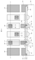
- FIG. 2 is a partially enlarged view of FIG. 1 and its cross-sectional view.
- the upper diagram in FIG. 2 is an enlarged view of the Al electrode group 113 in FIG. 1, and the lower diagram in FIG.
- the semiconductor device 112 of this embodiment has an anode electrode 106 provided in the central active region, and a polysilicon field plate 105 and an Al electrode 108 in the termination region provided on the outer periphery of the active region. have A guard ring 107 is provided on the outer periphery of the termination region.
- an embodiment applied to a diode is described, but the present invention is not limited to this, and may be applied to a switching element such as an IGBT or a MOSFET.
- the termination region comprises, as shown in FIG. 2, a p-type well layer 101 connected to an anode electrode 106 and a plurality of floating p-type field limiters on the surface of the n ⁇ layer substrate 100 to maintain a breakdown voltage.
- a thinning layer 102 and an n+ channel stopper layer 103 formed at the chip edge are provided.
- a p-type well layer 101 extends from the active region and is connected to an anode electrode 106 .
- Channel stopper layer 103 is connected to guard ring electrode 107 .
- the conductivity type (n, p) may be reversed.
- FIG. 2 shows a case where there are four field limiting layers 102, but the number of field limiting layers 102 is not limited as long as it is at least one.
- the field limiting layer 102 in the termination region is electrically connected to the polysilicon field plate 105 through the Al electrode 108.
- the Al electrode 108 is provided only on a part of the polysilicon field plate 105 in order to ensure high temperature and high humidity bias resistance.
- a contact 110 for connecting the Al electrode 108 and the field limiting layer 102 and a contact 109 for connecting the Al electrode 108 and the polysilicon field plate 105 are separately provided. That is, the interlayer film 104a is provided with a contact hole 114 for connecting the Al electrode 108 and the field plate 105 to form a contact 109, and the interlayer films 104a and 104b are provided with the Al electrode 108 and the field limiting layer.
- a contact hole 115 is provided to connect to and constitute a contact 110 .
- there is one contact between one Al electrode 108 and one polysilicon field plate 105 but the number of contacts may be one or more, and may be plural.
- the number of contacts should be one or more, and may be plural.
- a polysilicon extraction region 111 is provided around the contact 110 so that the polysilicon field plate 105 is not provided.
- the Al electrode groups are alternately arranged so that adjacent Al electrodes 108 are not arranged on a straight line. With such a configuration, it is possible to ensure a large distance between the adjacent Al electrodes and prevent the Al electrodes 108 from being corroded and melted due to the potential difference.
- the Al electrode is used to electrically connect the field limiting layer and the polysilicon field plate, but the connection between the field limiting layer and the Al electrode and the connection between the field plate and the Al electrode are different contacts.
- it is possible to reliably contact other than the side wall of the polysilicon field plate and suppress the contact resistance, so that good connection can be realized.
- the electric field applied between the Al electrodes can be relaxed, and high-temperature and high-humidity bias resistance can be ensured.
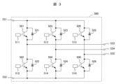
- FIG. 3 is a circuit diagram showing a schematic configuration of the power converter of the present invention.
- FIG. 3 shows an example of the circuit configuration of the power conversion device 500 of this embodiment and the relationship of connection between the DC power supply and the three-phase AC motor (AC load).
- AC load three-phase AC motor
- the semiconductor device of the present invention described above is used as any or all of the power switching elements 501-506 and the diodes 521-526.
- the power switching elements 501-506 are for example IGBTs and the elements 521-526 are diodes.
- the power conversion device 500 of the present embodiment includes a pair of DC terminals, namely, a P terminal 531 and an N terminal 532, and the same number of AC terminals as the number of AC output phases, a U terminal 533 and a V terminal. 534 and a W terminal 535 .
- It also has a switching leg that consists of a pair of power switching elements 501 and 502 connected in series, and that outputs a U terminal 533 connected to the series connection point. It also has a switching leg which is composed of a series connection of power switching elements 503 and 504 having the same configuration and outputs a V terminal 534 connected to the series connection point. A switching leg is also provided, which is composed of a series connection of power switching elements 505 and 506 having the same configuration and has a W terminal 535 connected to the series connection point as an output.
- a three-phase switching leg consisting of power switching elements 501 to 506 is connected between DC terminals of P terminal 531 and N terminal 532, and DC power is supplied from a DC power supply (not shown).
- a U terminal 533, a V terminal 534, and a W terminal 535, which are three-phase AC terminals of the power converter 500, are connected to a three-phase AC motor (not shown) as a three-phase AC power supply.
- a power switching element 501 and a diode 521 connected in antiparallel to the power switching element 501 are connected to form a parallel circuit.
- power switching element 502 and diode 522, power switching element 503 and diode 523, power switching element 504 and diode 524, power switching element 505 and diode 525, and power switching element 506 and diode 526 form a parallel circuit. It is connected to the.
- a parallel circuit including power switching element 501 and a parallel circuit including power switching element 502 are connected in series.
- a parallel circuit including power switching element 503 and a parallel circuit including power switching element 504 are connected in series
- a parallel circuit including power switching element 505 and a parallel circuit including power switching element 506 are connected in series. It is connected.
- Gate circuits 511 to 516 are connected to the input terminals of the gates of the power switching elements 501 to 506 made of IGBTs, and the power switching elements 501 to 506 are controlled by the gate circuits 511 to 516, respectively.
- the gate circuits 511 to 516 are centrally controlled by an overall control circuit (not shown).
- the gate circuits 511 to 516 collectively and appropriately control the power switching elements 501 to 506 to convert the DC power of the DC power supply into three-phase AC power, which is supplied from the U terminal 533, the V terminal 534, and the W terminal 535. output.
- a power conversion device that has higher temperature and humidity bias resistance than the conventional one and realizes a good connection between the field limiting layer and the field plate can be obtained. can provide.
- a semiconductor device capable of improving high-temperature and high-humidity bias resistance as compared with the prior art, and achieving good connection between the field limiting layer and the field plate, and power conversion using the semiconductor device. It was shown that the device can be provided.
- the present invention is not limited to the above-described embodiments, and includes various modifications.
- the above-described embodiments have been described in detail in order to explain the present invention in an easy-to-understand manner, and are not necessarily limited to those having all the described configurations.
- it is possible to replace part of the configuration of one embodiment with the configuration of another embodiment and it is also possible to add the configuration of another embodiment to the configuration of one embodiment.
Landscapes
- Engineering & Computer Science (AREA)
- Power Engineering (AREA)
- Electrodes Of Semiconductors (AREA)
- Bipolar Transistors (AREA)
- Emergency Protection Circuit Devices (AREA)
- Electronic Switches (AREA)
Abstract
Description
図3は本発明の電力変換装置の概略構成を示す回路図である。図3は、本実施形態の電力変換装置500の回路構成の一例と直流電源と三相交流モータ(交流負荷)との接続の関係を示す。
Claims (4)
- ターミネーション領域に設けられたフローティングのフィールドリミッティング層と、前記フィールドリミッティング層に電気的に接続されたフィールドプレートと、を備える半導体装置において、
前記フィールドプレートはポリシリコンにより形成され、
前記フィールドプレートと前記フィールドリミッティング層はAl電極を介して接続されており、
前記フィールドリミッティング層と前記Al電極との接続と、前記フィールドプレートと前記Al電極との接続は、異なるコンタクトで接続されていることを特徴とする半導体装置。 - 請求項1に記載の半導体装置において、
前記フィールドリミッティング層、前記フィールドプレートおよび前記Al電極はそれぞれ複数配置され、
複数の前記Al電極は、前記半導体装置の上面をみたときに、隣り合う前記Al電極が一直線上に並ばないように互い違いに配置されている電極群を構成することを特徴とする半導体装置。 - 請求項2に記載の半導体装置において、
互い違いに配置された複数の前記Al電極の電極群が複数配置されていることを特徴とする半導体装置。 - 一対の直流端子と、
交流出力の相数と同数の交流端子と、
前記一対の直流端子間に接続され、スイッチング素子と前記スイッチング素子に逆並列に接続されたダイオードとで構成された並列回路が2個直列に接続された、交流出力の相数と同数のスイッチングレッグと、
前記スイッチング素子を制御するゲート回路と、を有する電力変換装置であって、
前記スイッチング素子および前記ダイオードの少なくとも一方は、請求項1から3のいずれか1項に記載の半導体装置であることを特徴とする電力変換装置。
Priority Applications (3)
| Application Number | Priority Date | Filing Date | Title |
|---|---|---|---|
| CN202280051169.2A CN117813693A (zh) | 2021-12-13 | 2022-11-11 | 半导体器件和功率转换装置 |
| US18/683,523 US20240355888A1 (en) | 2021-12-13 | 2022-11-11 | Semiconductor device and power conversion device |
| EP22907101.4A EP4451342A4 (en) | 2021-12-13 | 2022-11-11 | SEMICONDUCTOR DEVICE AND POWER CONVERSION DEVICE |
Applications Claiming Priority (2)
| Application Number | Priority Date | Filing Date | Title |
|---|---|---|---|
| JP2021201431A JP7835974B2 (ja) | 2021-12-13 | 2021-12-13 | 半導体装置および電力変換装置 |
| JP2021-201431 | 2021-12-13 |
Publications (1)
| Publication Number | Publication Date |
|---|---|
| WO2023112570A1 true WO2023112570A1 (ja) | 2023-06-22 |
Family
ID=86774088
Family Applications (1)
| Application Number | Title | Priority Date | Filing Date |
|---|---|---|---|
| PCT/JP2022/042064 Ceased WO2023112570A1 (ja) | 2021-12-13 | 2022-11-11 | 半導体装置および電力変換装置 |
Country Status (6)
| Country | Link |
|---|---|
| US (1) | US20240355888A1 (ja) |
| EP (1) | EP4451342A4 (ja) |
| JP (1) | JP7835974B2 (ja) |
| CN (1) | CN117813693A (ja) |
| TW (1) | TWI838936B (ja) |
| WO (1) | WO2023112570A1 (ja) |
Families Citing this family (1)
| Publication number | Priority date | Publication date | Assignee | Title |
|---|---|---|---|---|
| CN115241280B (zh) * | 2022-07-05 | 2026-02-24 | 矽力杰半导体技术(杭州)有限公司 | 双向开关器件、其终端结构及电子设备 |
Citations (4)
| Publication number | Priority date | Publication date | Assignee | Title |
|---|---|---|---|---|
| WO2013140572A1 (ja) * | 2012-03-22 | 2013-09-26 | トヨタ自動車株式会社 | 半導体装置 |
| US20160013265A1 (en) * | 2011-07-19 | 2016-01-14 | Hamza Yilmaz | Semiconductor device with field threshold mosfet for high voltage termination |
| JP2016119434A (ja) * | 2014-12-24 | 2016-06-30 | 株式会社日立製作所 | 半導体装置、その製造方法、それを用いた電力変換装置 |
| US20190109230A1 (en) * | 2017-10-06 | 2019-04-11 | Infineon Technologies Austria Ag | High Voltage Termination Structure of a Power Semiconductor Device |
Family Cites Families (8)
| Publication number | Priority date | Publication date | Assignee | Title |
|---|---|---|---|---|
| JP3111827B2 (ja) * | 1994-09-20 | 2000-11-27 | 株式会社日立製作所 | 半導体装置及びそれを使った電力変換装置 |
| US8008734B2 (en) * | 2007-01-11 | 2011-08-30 | Fuji Electric Co., Ltd. | Power semiconductor device |
| JP5182766B2 (ja) * | 2009-12-16 | 2013-04-17 | 三菱電機株式会社 | 高耐圧半導体装置 |
| JP5611684B2 (ja) * | 2010-06-22 | 2014-10-22 | 株式会社東芝 | 電力変換装置 |
| JP5637154B2 (ja) * | 2012-02-22 | 2014-12-10 | トヨタ自動車株式会社 | 半導体装置 |
| JP6351331B2 (ja) * | 2014-03-28 | 2018-07-04 | 株式会社東芝 | 電力変換装置 |
| JP6287958B2 (ja) * | 2015-05-27 | 2018-03-07 | トヨタ自動車株式会社 | 半導体装置 |
| JP7735629B2 (ja) * | 2020-05-25 | 2025-09-09 | ミネベアパワーデバイス株式会社 | 半導体装置および電力変換装置 |
-
2021
- 2021-12-13 JP JP2021201431A patent/JP7835974B2/ja active Active
-
2022
- 2022-10-31 TW TW111141347A patent/TWI838936B/zh active
- 2022-11-11 EP EP22907101.4A patent/EP4451342A4/en active Pending
- 2022-11-11 WO PCT/JP2022/042064 patent/WO2023112570A1/ja not_active Ceased
- 2022-11-11 US US18/683,523 patent/US20240355888A1/en active Pending
- 2022-11-11 CN CN202280051169.2A patent/CN117813693A/zh active Pending
Patent Citations (4)
| Publication number | Priority date | Publication date | Assignee | Title |
|---|---|---|---|---|
| US20160013265A1 (en) * | 2011-07-19 | 2016-01-14 | Hamza Yilmaz | Semiconductor device with field threshold mosfet for high voltage termination |
| WO2013140572A1 (ja) * | 2012-03-22 | 2013-09-26 | トヨタ自動車株式会社 | 半導体装置 |
| JP2016119434A (ja) * | 2014-12-24 | 2016-06-30 | 株式会社日立製作所 | 半導体装置、その製造方法、それを用いた電力変換装置 |
| US20190109230A1 (en) * | 2017-10-06 | 2019-04-11 | Infineon Technologies Austria Ag | High Voltage Termination Structure of a Power Semiconductor Device |
Non-Patent Citations (1)
| Title |
|---|
| See also references of EP4451342A4 * |
Also Published As
| Publication number | Publication date |
|---|---|
| EP4451342A4 (en) | 2025-11-26 |
| TWI838936B (zh) | 2024-04-11 |
| US20240355888A1 (en) | 2024-10-24 |
| JP2023087192A (ja) | 2023-06-23 |
| CN117813693A (zh) | 2024-04-02 |
| EP4451342A1 (en) | 2024-10-23 |
| JP7835974B2 (ja) | 2026-03-26 |
| TW202339261A (zh) | 2023-10-01 |
Similar Documents
| Publication | Publication Date | Title |
|---|---|---|
| US20110215746A1 (en) | Semiconductor device | |
| US7808070B2 (en) | Power semiconductor component | |
| JP2007522677A (ja) | 集積型iii族−窒化物電力デバイス | |
| CN104011861B (zh) | 集成电路的单块单元并且尤其是单块转换单元 | |
| US11296601B2 (en) | Power transistor with distributed gate | |
| CN108463888A (zh) | 半导体装置 | |
| WO2015121899A1 (ja) | 電力用半導体モジュール | |
| JPH04361571A (ja) | Mos型半導体装置 | |
| CN103426910B (zh) | 功率半导体元件及其边缘终端结构 | |
| TW202339187A (zh) | 半導體裝置及電力轉換裝置 | |
| CN102024814B (zh) | Mos-栅功率半导体器件 | |
| WO2023112570A1 (ja) | 半導体装置および電力変換装置 | |
| KR101060127B1 (ko) | 모스 게이트 전력 반도체 소자 | |
| JP2023074722A (ja) | 半導体装置および電力変換装置 | |
| CN101236964B (zh) | 具有开关元件和两个二极管的半导体装置 | |
| US9654027B2 (en) | Semiconductor device and power converter using the same | |
| US12334427B2 (en) | Semiconductor device | |
| JP2020099039A (ja) | 双方向スイッチ | |
| WO1996029744A1 (en) | Planar semiconductor device, its manufacturing method, and power converter | |
| EP4425780A1 (en) | Semiconductor arrangement and semiconductor module arrangement | |
| JP2023003564A (ja) | 半導体装置 | |
| JP2020035946A (ja) | 電力用半導体装置、電力変換装置、電力用半導体装置の製造方法、および、電力変換装置の製造方法 | |
| CN107924874A (zh) | 复合型半导体装置 | |
| WO1999054940A1 (fr) | Dispositif semiconducteur composite |
Legal Events
| Date | Code | Title | Description |
|---|---|---|---|
| 121 | Ep: the epo has been informed by wipo that ep was designated in this application |
Ref document number: 22907101 Country of ref document: EP Kind code of ref document: A1 |
|
| WWE | Wipo information: entry into national phase |
Ref document number: 202280051169.2 Country of ref document: CN |
|
| WWE | Wipo information: entry into national phase |
Ref document number: 18683523 Country of ref document: US |
|
| WWE | Wipo information: entry into national phase |
Ref document number: 2022907101 Country of ref document: EP |
|
| NENP | Non-entry into the national phase |
Ref country code: DE |
|
| ENP | Entry into the national phase |
Ref document number: 2022907101 Country of ref document: EP Effective date: 20240715 |