WO2023144867A1 - 切削工具及びその製造方法 - Google Patents
切削工具及びその製造方法 Download PDFInfo
- Publication number
- WO2023144867A1 WO2023144867A1 PCT/JP2022/002579 JP2022002579W WO2023144867A1 WO 2023144867 A1 WO2023144867 A1 WO 2023144867A1 JP 2022002579 W JP2022002579 W JP 2022002579W WO 2023144867 A1 WO2023144867 A1 WO 2023144867A1
- Authority
- WO
- WIPO (PCT)
- Prior art keywords
- layer
- less
- silicon
- cutting tool
- hard particles
- Prior art date
- Legal status (The legal status is an assumption and is not a legal conclusion. Google has not performed a legal analysis and makes no representation as to the accuracy of the status listed.)
- Ceased
Links
Images



Classifications
-
- C—CHEMISTRY; METALLURGY
- C23—COATING METALLIC MATERIAL; COATING MATERIAL WITH METALLIC MATERIAL; CHEMICAL SURFACE TREATMENT; DIFFUSION TREATMENT OF METALLIC MATERIAL; COATING BY VACUUM EVAPORATION, BY SPUTTERING, BY ION IMPLANTATION OR BY CHEMICAL VAPOUR DEPOSITION, IN GENERAL; INHIBITING CORROSION OF METALLIC MATERIAL OR INCRUSTATION IN GENERAL
- C23C—COATING METALLIC MATERIAL; COATING MATERIAL WITH METALLIC MATERIAL; SURFACE TREATMENT OF METALLIC MATERIAL BY DIFFUSION INTO THE SURFACE, BY CHEMICAL CONVERSION OR SUBSTITUTION; COATING BY VACUUM EVAPORATION, BY SPUTTERING, BY ION IMPLANTATION OR BY CHEMICAL VAPOUR DEPOSITION, IN GENERAL
- C23C16/00—Chemical coating by decomposition of gaseous compounds, without leaving reaction products of surface material in the coating, i.e. chemical vapour deposition [CVD] processes
- C23C16/44—Chemical coating by decomposition of gaseous compounds, without leaving reaction products of surface material in the coating, i.e. chemical vapour deposition [CVD] processes characterised by the method of coating
- C23C16/458—Chemical coating by decomposition of gaseous compounds, without leaving reaction products of surface material in the coating, i.e. chemical vapour deposition [CVD] processes characterised by the method of coating characterised by the method used for supporting substrates in the reaction chamber
- C23C16/4582—Rigid and flat substrates, e.g. plates or discs
- C23C16/4583—Rigid and flat substrates, e.g. plates or discs the substrate being supported substantially horizontally
- C23C16/4584—Rigid and flat substrates, e.g. plates or discs the substrate being supported substantially horizontally the substrate being rotated
-
- B—PERFORMING OPERATIONS; TRANSPORTING
- B23—MACHINE TOOLS; METAL-WORKING NOT OTHERWISE PROVIDED FOR
- B23B—TURNING; BORING
- B23B27/00—Tools for turning or boring machines; Tools of a similar kind in general; Accessories therefor
- B23B27/14—Cutting tools of which the bits or tips or cutting inserts are of special material
- B23B27/148—Composition of the cutting inserts
-
- C—CHEMISTRY; METALLURGY
- C23—COATING METALLIC MATERIAL; COATING MATERIAL WITH METALLIC MATERIAL; CHEMICAL SURFACE TREATMENT; DIFFUSION TREATMENT OF METALLIC MATERIAL; COATING BY VACUUM EVAPORATION, BY SPUTTERING, BY ION IMPLANTATION OR BY CHEMICAL VAPOUR DEPOSITION, IN GENERAL; INHIBITING CORROSION OF METALLIC MATERIAL OR INCRUSTATION IN GENERAL
- C23C—COATING METALLIC MATERIAL; COATING MATERIAL WITH METALLIC MATERIAL; SURFACE TREATMENT OF METALLIC MATERIAL BY DIFFUSION INTO THE SURFACE, BY CHEMICAL CONVERSION OR SUBSTITUTION; COATING BY VACUUM EVAPORATION, BY SPUTTERING, BY ION IMPLANTATION OR BY CHEMICAL VAPOUR DEPOSITION, IN GENERAL
- C23C16/00—Chemical coating by decomposition of gaseous compounds, without leaving reaction products of surface material in the coating, i.e. chemical vapour deposition [CVD] processes
- C23C16/22—Chemical coating by decomposition of gaseous compounds, without leaving reaction products of surface material in the coating, i.e. chemical vapour deposition [CVD] processes characterised by the deposition of inorganic material, other than metallic material
- C23C16/30—Deposition of compounds, mixtures or solid solutions, e.g. borides, carbides, nitrides
-
- C—CHEMISTRY; METALLURGY
- C23—COATING METALLIC MATERIAL; COATING MATERIAL WITH METALLIC MATERIAL; CHEMICAL SURFACE TREATMENT; DIFFUSION TREATMENT OF METALLIC MATERIAL; COATING BY VACUUM EVAPORATION, BY SPUTTERING, BY ION IMPLANTATION OR BY CHEMICAL VAPOUR DEPOSITION, IN GENERAL; INHIBITING CORROSION OF METALLIC MATERIAL OR INCRUSTATION IN GENERAL
- C23C—COATING METALLIC MATERIAL; COATING MATERIAL WITH METALLIC MATERIAL; SURFACE TREATMENT OF METALLIC MATERIAL BY DIFFUSION INTO THE SURFACE, BY CHEMICAL CONVERSION OR SUBSTITUTION; COATING BY VACUUM EVAPORATION, BY SPUTTERING, BY ION IMPLANTATION OR BY CHEMICAL VAPOUR DEPOSITION, IN GENERAL
- C23C16/00—Chemical coating by decomposition of gaseous compounds, without leaving reaction products of surface material in the coating, i.e. chemical vapour deposition [CVD] processes
- C23C16/22—Chemical coating by decomposition of gaseous compounds, without leaving reaction products of surface material in the coating, i.e. chemical vapour deposition [CVD] processes characterised by the deposition of inorganic material, other than metallic material
- C23C16/30—Deposition of compounds, mixtures or solid solutions, e.g. borides, carbides, nitrides
- C23C16/34—Nitrides
-
- C—CHEMISTRY; METALLURGY
- C23—COATING METALLIC MATERIAL; COATING MATERIAL WITH METALLIC MATERIAL; CHEMICAL SURFACE TREATMENT; DIFFUSION TREATMENT OF METALLIC MATERIAL; COATING BY VACUUM EVAPORATION, BY SPUTTERING, BY ION IMPLANTATION OR BY CHEMICAL VAPOUR DEPOSITION, IN GENERAL; INHIBITING CORROSION OF METALLIC MATERIAL OR INCRUSTATION IN GENERAL
- C23C—COATING METALLIC MATERIAL; COATING MATERIAL WITH METALLIC MATERIAL; SURFACE TREATMENT OF METALLIC MATERIAL BY DIFFUSION INTO THE SURFACE, BY CHEMICAL CONVERSION OR SUBSTITUTION; COATING BY VACUUM EVAPORATION, BY SPUTTERING, BY ION IMPLANTATION OR BY CHEMICAL VAPOUR DEPOSITION, IN GENERAL
- C23C16/00—Chemical coating by decomposition of gaseous compounds, without leaving reaction products of surface material in the coating, i.e. chemical vapour deposition [CVD] processes
- C23C16/22—Chemical coating by decomposition of gaseous compounds, without leaving reaction products of surface material in the coating, i.e. chemical vapour deposition [CVD] processes characterised by the deposition of inorganic material, other than metallic material
- C23C16/30—Deposition of compounds, mixtures or solid solutions, e.g. borides, carbides, nitrides
- C23C16/36—Carbonitrides
-
- C—CHEMISTRY; METALLURGY
- C23—COATING METALLIC MATERIAL; COATING MATERIAL WITH METALLIC MATERIAL; CHEMICAL SURFACE TREATMENT; DIFFUSION TREATMENT OF METALLIC MATERIAL; COATING BY VACUUM EVAPORATION, BY SPUTTERING, BY ION IMPLANTATION OR BY CHEMICAL VAPOUR DEPOSITION, IN GENERAL; INHIBITING CORROSION OF METALLIC MATERIAL OR INCRUSTATION IN GENERAL
- C23C—COATING METALLIC MATERIAL; COATING MATERIAL WITH METALLIC MATERIAL; SURFACE TREATMENT OF METALLIC MATERIAL BY DIFFUSION INTO THE SURFACE, BY CHEMICAL CONVERSION OR SUBSTITUTION; COATING BY VACUUM EVAPORATION, BY SPUTTERING, BY ION IMPLANTATION OR BY CHEMICAL VAPOUR DEPOSITION, IN GENERAL
- C23C16/00—Chemical coating by decomposition of gaseous compounds, without leaving reaction products of surface material in the coating, i.e. chemical vapour deposition [CVD] processes
- C23C16/22—Chemical coating by decomposition of gaseous compounds, without leaving reaction products of surface material in the coating, i.e. chemical vapour deposition [CVD] processes characterised by the deposition of inorganic material, other than metallic material
- C23C16/30—Deposition of compounds, mixtures or solid solutions, e.g. borides, carbides, nitrides
- C23C16/40—Oxides
- C23C16/403—Oxides of aluminium, magnesium or beryllium
-
- C—CHEMISTRY; METALLURGY
- C23—COATING METALLIC MATERIAL; COATING MATERIAL WITH METALLIC MATERIAL; CHEMICAL SURFACE TREATMENT; DIFFUSION TREATMENT OF METALLIC MATERIAL; COATING BY VACUUM EVAPORATION, BY SPUTTERING, BY ION IMPLANTATION OR BY CHEMICAL VAPOUR DEPOSITION, IN GENERAL; INHIBITING CORROSION OF METALLIC MATERIAL OR INCRUSTATION IN GENERAL
- C23C—COATING METALLIC MATERIAL; COATING MATERIAL WITH METALLIC MATERIAL; SURFACE TREATMENT OF METALLIC MATERIAL BY DIFFUSION INTO THE SURFACE, BY CHEMICAL CONVERSION OR SUBSTITUTION; COATING BY VACUUM EVAPORATION, BY SPUTTERING, BY ION IMPLANTATION OR BY CHEMICAL VAPOUR DEPOSITION, IN GENERAL
- C23C16/00—Chemical coating by decomposition of gaseous compounds, without leaving reaction products of surface material in the coating, i.e. chemical vapour deposition [CVD] processes
- C23C16/44—Chemical coating by decomposition of gaseous compounds, without leaving reaction products of surface material in the coating, i.e. chemical vapour deposition [CVD] processes characterised by the method of coating
- C23C16/455—Chemical coating by decomposition of gaseous compounds, without leaving reaction products of surface material in the coating, i.e. chemical vapour deposition [CVD] processes characterised by the method of coating characterised by the method used for introducing gases into reaction chamber or for modifying gas flows in reaction chamber
- C23C16/45502—Flow conditions in reaction chamber
- C23C16/45508—Radial flow
-
- C—CHEMISTRY; METALLURGY
- C23—COATING METALLIC MATERIAL; COATING MATERIAL WITH METALLIC MATERIAL; CHEMICAL SURFACE TREATMENT; DIFFUSION TREATMENT OF METALLIC MATERIAL; COATING BY VACUUM EVAPORATION, BY SPUTTERING, BY ION IMPLANTATION OR BY CHEMICAL VAPOUR DEPOSITION, IN GENERAL; INHIBITING CORROSION OF METALLIC MATERIAL OR INCRUSTATION IN GENERAL
- C23C—COATING METALLIC MATERIAL; COATING MATERIAL WITH METALLIC MATERIAL; SURFACE TREATMENT OF METALLIC MATERIAL BY DIFFUSION INTO THE SURFACE, BY CHEMICAL CONVERSION OR SUBSTITUTION; COATING BY VACUUM EVAPORATION, BY SPUTTERING, BY ION IMPLANTATION OR BY CHEMICAL VAPOUR DEPOSITION, IN GENERAL
- C23C16/00—Chemical coating by decomposition of gaseous compounds, without leaving reaction products of surface material in the coating, i.e. chemical vapour deposition [CVD] processes
- C23C16/44—Chemical coating by decomposition of gaseous compounds, without leaving reaction products of surface material in the coating, i.e. chemical vapour deposition [CVD] processes characterised by the method of coating
- C23C16/455—Chemical coating by decomposition of gaseous compounds, without leaving reaction products of surface material in the coating, i.e. chemical vapour deposition [CVD] processes characterised by the method of coating characterised by the method used for introducing gases into reaction chamber or for modifying gas flows in reaction chamber
- C23C16/45523—Pulsed gas flow or change of composition over time
-
- C—CHEMISTRY; METALLURGY
- C23—COATING METALLIC MATERIAL; COATING MATERIAL WITH METALLIC MATERIAL; CHEMICAL SURFACE TREATMENT; DIFFUSION TREATMENT OF METALLIC MATERIAL; COATING BY VACUUM EVAPORATION, BY SPUTTERING, BY ION IMPLANTATION OR BY CHEMICAL VAPOUR DEPOSITION, IN GENERAL; INHIBITING CORROSION OF METALLIC MATERIAL OR INCRUSTATION IN GENERAL
- C23C—COATING METALLIC MATERIAL; COATING MATERIAL WITH METALLIC MATERIAL; SURFACE TREATMENT OF METALLIC MATERIAL BY DIFFUSION INTO THE SURFACE, BY CHEMICAL CONVERSION OR SUBSTITUTION; COATING BY VACUUM EVAPORATION, BY SPUTTERING, BY ION IMPLANTATION OR BY CHEMICAL VAPOUR DEPOSITION, IN GENERAL
- C23C16/00—Chemical coating by decomposition of gaseous compounds, without leaving reaction products of surface material in the coating, i.e. chemical vapour deposition [CVD] processes
- C23C16/44—Chemical coating by decomposition of gaseous compounds, without leaving reaction products of surface material in the coating, i.e. chemical vapour deposition [CVD] processes characterised by the method of coating
- C23C16/455—Chemical coating by decomposition of gaseous compounds, without leaving reaction products of surface material in the coating, i.e. chemical vapour deposition [CVD] processes characterised by the method of coating characterised by the method used for introducing gases into reaction chamber or for modifying gas flows in reaction chamber
- C23C16/45563—Gas nozzles
- C23C16/45576—Coaxial inlets for each gas
-
- C—CHEMISTRY; METALLURGY
- C23—COATING METALLIC MATERIAL; COATING MATERIAL WITH METALLIC MATERIAL; CHEMICAL SURFACE TREATMENT; DIFFUSION TREATMENT OF METALLIC MATERIAL; COATING BY VACUUM EVAPORATION, BY SPUTTERING, BY ION IMPLANTATION OR BY CHEMICAL VAPOUR DEPOSITION, IN GENERAL; INHIBITING CORROSION OF METALLIC MATERIAL OR INCRUSTATION IN GENERAL
- C23C—COATING METALLIC MATERIAL; COATING MATERIAL WITH METALLIC MATERIAL; SURFACE TREATMENT OF METALLIC MATERIAL BY DIFFUSION INTO THE SURFACE, BY CHEMICAL CONVERSION OR SUBSTITUTION; COATING BY VACUUM EVAPORATION, BY SPUTTERING, BY ION IMPLANTATION OR BY CHEMICAL VAPOUR DEPOSITION, IN GENERAL
- C23C16/00—Chemical coating by decomposition of gaseous compounds, without leaving reaction products of surface material in the coating, i.e. chemical vapour deposition [CVD] processes
- C23C16/44—Chemical coating by decomposition of gaseous compounds, without leaving reaction products of surface material in the coating, i.e. chemical vapour deposition [CVD] processes characterised by the method of coating
- C23C16/455—Chemical coating by decomposition of gaseous compounds, without leaving reaction products of surface material in the coating, i.e. chemical vapour deposition [CVD] processes characterised by the method of coating characterised by the method used for introducing gases into reaction chamber or for modifying gas flows in reaction chamber
- C23C16/45563—Gas nozzles
- C23C16/45578—Elongated nozzles, tubes with holes
-
- C—CHEMISTRY; METALLURGY
- C23—COATING METALLIC MATERIAL; COATING MATERIAL WITH METALLIC MATERIAL; CHEMICAL SURFACE TREATMENT; DIFFUSION TREATMENT OF METALLIC MATERIAL; COATING BY VACUUM EVAPORATION, BY SPUTTERING, BY ION IMPLANTATION OR BY CHEMICAL VAPOUR DEPOSITION, IN GENERAL; INHIBITING CORROSION OF METALLIC MATERIAL OR INCRUSTATION IN GENERAL
- C23C—COATING METALLIC MATERIAL; COATING MATERIAL WITH METALLIC MATERIAL; SURFACE TREATMENT OF METALLIC MATERIAL BY DIFFUSION INTO THE SURFACE, BY CHEMICAL CONVERSION OR SUBSTITUTION; COATING BY VACUUM EVAPORATION, BY SPUTTERING, BY ION IMPLANTATION OR BY CHEMICAL VAPOUR DEPOSITION, IN GENERAL
- C23C16/00—Chemical coating by decomposition of gaseous compounds, without leaving reaction products of surface material in the coating, i.e. chemical vapour deposition [CVD] processes
- C23C16/56—After-treatment
-
- C—CHEMISTRY; METALLURGY
- C23—COATING METALLIC MATERIAL; COATING MATERIAL WITH METALLIC MATERIAL; CHEMICAL SURFACE TREATMENT; DIFFUSION TREATMENT OF METALLIC MATERIAL; COATING BY VACUUM EVAPORATION, BY SPUTTERING, BY ION IMPLANTATION OR BY CHEMICAL VAPOUR DEPOSITION, IN GENERAL; INHIBITING CORROSION OF METALLIC MATERIAL OR INCRUSTATION IN GENERAL
- C23C—COATING METALLIC MATERIAL; COATING MATERIAL WITH METALLIC MATERIAL; SURFACE TREATMENT OF METALLIC MATERIAL BY DIFFUSION INTO THE SURFACE, BY CHEMICAL CONVERSION OR SUBSTITUTION; COATING BY VACUUM EVAPORATION, BY SPUTTERING, BY ION IMPLANTATION OR BY CHEMICAL VAPOUR DEPOSITION, IN GENERAL
- C23C28/00—Coating for obtaining at least two superposed coatings either by methods not provided for in a single one of groups C23C2/00 - C23C26/00 or by combinations of methods provided for in subclasses C23C and C25C or C25D
- C23C28/04—Coating for obtaining at least two superposed coatings either by methods not provided for in a single one of groups C23C2/00 - C23C26/00 or by combinations of methods provided for in subclasses C23C and C25C or C25D only coatings of inorganic non-metallic material
-
- C—CHEMISTRY; METALLURGY
- C23—COATING METALLIC MATERIAL; COATING MATERIAL WITH METALLIC MATERIAL; CHEMICAL SURFACE TREATMENT; DIFFUSION TREATMENT OF METALLIC MATERIAL; COATING BY VACUUM EVAPORATION, BY SPUTTERING, BY ION IMPLANTATION OR BY CHEMICAL VAPOUR DEPOSITION, IN GENERAL; INHIBITING CORROSION OF METALLIC MATERIAL OR INCRUSTATION IN GENERAL
- C23C—COATING METALLIC MATERIAL; COATING MATERIAL WITH METALLIC MATERIAL; SURFACE TREATMENT OF METALLIC MATERIAL BY DIFFUSION INTO THE SURFACE, BY CHEMICAL CONVERSION OR SUBSTITUTION; COATING BY VACUUM EVAPORATION, BY SPUTTERING, BY ION IMPLANTATION OR BY CHEMICAL VAPOUR DEPOSITION, IN GENERAL
- C23C28/00—Coating for obtaining at least two superposed coatings either by methods not provided for in a single one of groups C23C2/00 - C23C26/00 or by combinations of methods provided for in subclasses C23C and C25C or C25D
- C23C28/04—Coating for obtaining at least two superposed coatings either by methods not provided for in a single one of groups C23C2/00 - C23C26/00 or by combinations of methods provided for in subclasses C23C and C25C or C25D only coatings of inorganic non-metallic material
- C23C28/044—Coating for obtaining at least two superposed coatings either by methods not provided for in a single one of groups C23C2/00 - C23C26/00 or by combinations of methods provided for in subclasses C23C and C25C or C25D only coatings of inorganic non-metallic material coatings specially adapted for cutting tools or wear applications
-
- C—CHEMISTRY; METALLURGY
- C23—COATING METALLIC MATERIAL; COATING MATERIAL WITH METALLIC MATERIAL; CHEMICAL SURFACE TREATMENT; DIFFUSION TREATMENT OF METALLIC MATERIAL; COATING BY VACUUM EVAPORATION, BY SPUTTERING, BY ION IMPLANTATION OR BY CHEMICAL VAPOUR DEPOSITION, IN GENERAL; INHIBITING CORROSION OF METALLIC MATERIAL OR INCRUSTATION IN GENERAL
- C23C—COATING METALLIC MATERIAL; COATING MATERIAL WITH METALLIC MATERIAL; SURFACE TREATMENT OF METALLIC MATERIAL BY DIFFUSION INTO THE SURFACE, BY CHEMICAL CONVERSION OR SUBSTITUTION; COATING BY VACUUM EVAPORATION, BY SPUTTERING, BY ION IMPLANTATION OR BY CHEMICAL VAPOUR DEPOSITION, IN GENERAL
- C23C30/00—Coating with metallic material characterised only by the composition of the metallic material, i.e. not characterised by the coating process
- C23C30/005—Coating with metallic material characterised only by the composition of the metallic material, i.e. not characterised by the coating process on hard metal substrates
-
- B—PERFORMING OPERATIONS; TRANSPORTING
- B23—MACHINE TOOLS; METAL-WORKING NOT OTHERWISE PROVIDED FOR
- B23B—TURNING; BORING
- B23B2228/00—Properties of materials of tools or workpieces, materials of tools or workpieces applied in a specific manner
- B23B2228/10—Coatings
- B23B2228/105—Coatings with specified thickness
Definitions
- the present disclosure relates to cutting tools and manufacturing methods thereof.
- US Pat. No. 5,300,001 discloses a nanocomposite coating comprising a nanocrystalline layer of TiC x N 1-x and a second phase of amorphous SiC x N y produced by thermal CVD.
- Patent Document 2 discloses at least a first nanocrystalline phase made of cubic titanium oxycarbonitride produced by a thermal CVD method and a second amorphous phase made of silicon oxycarbonitride or silicon oxycarbide.
- One nanocomposite layer is disclosed.
- Non-Patent Document 1 discloses a TiSiCN film having a nanocomposite structure formed by the PVD method.
- the present disclosure provides a cutting tool that includes a substrate and a coating disposed on the substrate, comprising:
- the coating comprises a first layer of hard particles,
- the hard particles are made of TiSiCN having a cubic crystal structure,
- the hard particles have a lamellar structure in which layers with a relatively high silicon concentration and layers with a relatively low silicon concentration are alternately laminated,
- the maximum value of the percentage ⁇ A Si /(A Si +A Ti ) ⁇ 100 of the number of silicon atoms A Si with respect to the sum of the number of silicon atoms A Si and the number of titanium atoms A Ti in the grain boundary region between the hard grains is the percentage ⁇ B Si /(B Si +B Ti ) ⁇ 100 of the number of silicon atoms B Si to the sum of the number of silicon atoms B Si and the number B Ti of titanium atoms in the first layer big, A cutting tool.
- the present disclosure provides a method for manufacturing the cutting tool, a first step of preparing a substrate; a second step of forming a coating on the substrate; A third step of heat-treating the coating to obtain a cutting tool,
- the coating formed in the second step comprises a first layer composed of a plurality of hard particles,
- the hard particles are made of TiSiCN having a cubic crystal structure,
- the hard particles have a lamellar structure in which a layer having a relatively high silicon concentration and a layer having a relatively low silicon concentration are alternately laminated.
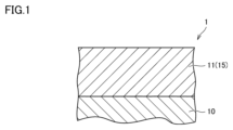
- FIG. 1 is a schematic diagram showing an example of a cross section of a cutting tool according to Embodiment 1.
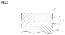
- FIG. FIG. 2 is a schematic diagram showing another example of the cross section of the cutting tool according to Embodiment 1.
- FIG. 3 is a schematic diagram showing another example of the cross section of the cutting tool according to Embodiment 1.
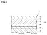
- FIG. 4 is a schematic diagram showing another example of the cross section of the cutting tool according to Embodiment 1.
- FIG. 5 is a diagram schematically showing another example of the cross section of the cutting tool according to Embodiment 1.
- FIG. FIG. 6 is an enlarged view of a rectangular portion surrounded by a frame indicated by symbol a1 in FIG. FIG.
- FIG. 7 is an enlarged view of a rectangular portion enclosed by a frame indicated by reference numeral a2 in FIG. 8 is a diagram showing an example of a high-angle annular dark-field scanning transmission electron microscope (HAADF-STEM) image of a cross section of the first layer of the cutting tool according to Embodiment 1.
- FIG. 9 is an electron diffraction image taken within the region A shown in FIG.
- FIG. 10 is a graph showing the results of line analysis along the arrow directions shown in FIG.
- FIG. 11 is a Fourier transform image obtained by Fourier transforming the area A shown in FIG. 12 is a graph showing the intensity profile within the square frame of the Fourier transform image of FIG. 11.
- FIG. 13 is a diagram showing an example of an STEM image of the cutting tool according to Embodiment 1.
- FIG. 14 is a diagram showing an HAADF-STEM image including grain boundary regions observed in FIG.
- FIG. 15 is a graph showing the results of line analysis along line L2 in FIG.
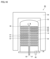
- FIG. 16 is a schematic cross-sectional view of an example of a CVD apparatus used in the method of manufacturing a cutting tool according to Embodiment 2.
- the purpose is to provide a cutting tool that can have a long tool life in high-efficiency machining in general.
- the present disclosure provides a cutting tool comprising a substrate and a coating disposed on the substrate,
- the coating comprises a first layer of hard particles,
- the hard particles are made of TiSiCN having a cubic crystal structure,
- the hard particles have a lamellar structure in which layers with a relatively high silicon concentration and layers with a relatively low silicon concentration are alternately laminated,
- the maximum value of the percentage ⁇ A Si /(A Si +A Ti ) ⁇ 100 of the number of silicon atoms A Si with respect to the sum of the number of silicon atoms A Si and the number of titanium atoms A Ti in the grain boundary region between the hard grains is the percentage ⁇ B Si /(B Si +B Ti ) ⁇ 100 of the number of silicon atoms B Si to the sum of the number of silicon atoms B Si and the number B Ti of titanium atoms in the first layer big, A cutting tool.
- the average value of the percentage ⁇ B Si /(B Si +B Ti ) ⁇ 100 is preferably 0.5% or more and 10% or less. According to this, the tool life is further improved.
- the thickness of the first layer is 3 ⁇ m or more and 15 ⁇ m or less;
- the thickness of the coating is preferably 3 ⁇ m or more and 30 ⁇ m or less. According to this, the tool life is further improved.
- the maximum value of the percentage ⁇ A Si /(A Si +A Ti ) ⁇ 100 is obtained by using STEM-EDX with respect to the grain boundary region in a cross section along the normal line of the coating surface. Measured by line analysis with a length of 60 nm or more in the direction perpendicular to the direction of elongation of the grain boundary region, The average value of the percentage ⁇ B Si /(B Si +B Ti ) ⁇ ⁇ 100 is obtained using STEM-EDX in the cross section with respect to a rectangular measurement field of 100 nm ⁇ 100 nm provided in the first layer. is preferably determined by performing a rectangular analysis on the According to this, the accuracy of the measurement result is good.
- the hard particles preferably have an average aspect ratio of 2 or more. According to this, the tool life is further improved.
- the present disclosure provides a method for manufacturing the cutting tool, a first step of preparing a substrate; a second step of forming a coating on the substrate; A third step of heat-treating the coating to obtain a cutting tool,
- the coating formed in the second step comprises a first layer composed of a plurality of hard particles,
- the hard particles are made of TiSiCN having a cubic crystal structure,
- the hard particles have a lamellar structure in which a layer having a relatively high silicon concentration and a layer having a relatively low silicon concentration are alternately laminated.
- the heat treatment in the third step preferably includes a step of heating the film at 1050° C. or higher and 1100° C. or lower in a hydrogen atmosphere at a pressure of 850 hPa or higher and 950 hPa or lower for 5 minutes or longer and 30 minutes or shorter. This promotes the migration of silicon in the hard grains to the grain boundary region.
- the second step includes a step 2a of forming the first layer by a CVD method using a CVD apparatus
- the 2a step includes a 2a-1 step of ejecting TiCl 4 gas, SiCl 4 gas and CH 3 CN gas toward the surface of the base material,
- the TiCl 4 gas is jetted from a plurality of first injection holes provided in the nozzle of the CVD apparatus
- the SiCl 4 gas is jetted from a plurality of second injection holes provided in the nozzle
- the CH 3 CN gas is jetted from a plurality of third injection holes provided in the nozzle
- the nozzle rotates, the plurality of second injection holes include a 2-1 injection hole and a 2-2 injection hole,
- the diameter r1 of the 2-1 injection hole is preferably different from the diameter r2 of the 2-2 injection hole.
- a compound or the like when represented by a chemical formula, it shall include any conventionally known atomic ratio unless the atomic ratio is particularly limited, and should not necessarily be limited only to those within the stoichiometric range.
- TiSiCN the ratio of the number of atoms constituting TiSiCN includes all conventionally known atomic ratios.
- a cutting tool of one embodiment of the present disclosure (hereinafter also referred to as "this embodiment") is A cutting tool comprising a substrate and a coating disposed on the substrate, The coating comprises a first layer of hard particles, The hard particles consist of TiSiCN having a cubic crystal structure, The hard particles have a lamellar structure in which layers with a relatively high silicon concentration and layers with a relatively low silicon concentration are alternately laminated,
- the maximum value of the percentage ⁇ A Si /(A Si +A Ti ) ⁇ 100 of the number of silicon atoms A Si to the sum of the number of silicon atoms A Si and the number of titanium atoms A Ti in the grain boundary region between the hard grains is the percentage ⁇ B Si /(B Si +B Ti ) ⁇ 100 of the number of silicon atoms B Si to the sum of the number of silicon atoms B Si and the number B Ti of titanium atoms in the first layer A large cutting tool.
- the cutting tool of this embodiment can have a long tool life in high-efficiency machining in general. Although the reason for this is not clear, it is presumed as follows (i) to (v).
- the coating comprises a first layer made of hard particles. Since the hard particles are made of TiSiCN, the first layer can have regions made of columnar crystals extending in the thickness direction (hereinafter also referred to as "columnar structure"). This improves the toughness of the first layer, and even if thermal cracks occur on the surface of the coating due to cutting, the cracks are effectively suppressed from progressing to the substrate. Furthermore, since the first layer has a columnar structure, the direction of crack growth has anisotropy, so the peeling resistance of the coating is improved. Therefore, the cutting tool can have a long tool life.
- the hard particles are made of TiSiCN having a cubic crystal structure.
- the hard particles have high hardness.
- the first layer made of hard particles has high hardness and excellent wear resistance. Therefore, the cutting tool can have a long tool life.
- the hard particles have a lamellar structure in which layers with relatively high silicon concentration and layers with relatively low silicon concentration are alternately laminated. According to this, even if strain occurs in the hard particles and cracks are generated on the surface of the coating due to cutting, the propagation of the cracks to the base material is effectively suppressed. Moreover, the hardness of the hard particles and the first layer increases, and the wear resistance of the cutting tool improves. Therefore, the cutting tool can have a long tool life.
- the percentage of the number of silicon atoms A Si with respect to the sum of the number of silicon atoms A Si and the number of titanium atoms A Ti in the grain boundary region between the hard particles ⁇ A Si /(A Si +A Ti ) ⁇ 100 is the number of silicon atoms B Si and the number B of titanium atoms in the first layer. Larger than the average value of the percentage of the number of silicon atoms B Si to the total of Ti ⁇ B Si /(B Si +B Ti ) ⁇ 100 (hereinafter also referred to as “the average value of the silicon content in the first layer”) .
- the maximum silicon content in the grain boundary regions between the hard grains is greater than the average silicon content in the first layer. According to this, a concentration gradient of silicon occurs in the vicinity of the grain boundaries between hard particles, and along with this, the lattice constant changes in the vicinity of the grain boundaries, resulting in strain. Propagation of cracks is suppressed by the strain. Therefore, the cutting tool can have a long tool life.
- the maximum silicon content in grain boundary regions between hard particles is larger than the average silicon content in the first layer.
- Silicon present in the grain boundary region combines with oxygen that enters the inside of the coating along the grain boundary during high-efficiency machining of the work material. This suppresses oxidation of the hard particles and/or substrate. Therefore, the cutting tool can have a long tool life.
- the cutting tool 1 of this embodiment includes a substrate 10 and a coating 15 placed on the substrate 10 .
- FIG. 1 shows the case where the film 15 is composed only of the first layer 11 .
- the film 15 preferably covers at least a portion of the substrate involved in cutting, and more preferably covers the entire surface of the substrate.
- the portion involved in cutting of the substrate means a region within 500 ⁇ m from the ridgeline of the cutting edge on the surface of the substrate. It would not depart from the scope of the present disclosure if portions of the substrate were not coated with this coating or if the composition of the coating varied.
- Cutting tools of the present disclosure include, for example, drills, end mills (e.g., ball end mills), indexable cutting inserts for drills, indexable cutting inserts for end mills, indexable cutting inserts for milling, indexable cutting inserts for turning. It can be a cutting tip, metal saw, gear cutting tool, reamer, tap, or the like.
- the substrate 10 includes a rake face and a flank, and any conventionally known substrate of this type can be used.
- cemented carbide for example, WC-based cemented carbide containing tungsten carbide and cobalt, the cemented carbide may contain carbonitrides such as Ti, Ta, Nb), cermet (TiC, TiN, TiCN etc.), high speed steel, ceramics (titanium carbide, silicon carbide, silicon nitride, aluminum nitride, aluminum oxide, etc.), cubic boron nitride sintered body or diamond sintered body is preferred.
- a substrate made of a cemented carbide containing tungsten carbide and cobalt, in which the content of cobalt in the cemented carbide is 6% by mass or more and 11% by mass or less, is preferable. According to this, it has an excellent balance of hardness and strength at high temperatures, and has excellent properties as a base material for cutting tools for the above applications.
- a WC-based cemented carbide When a WC-based cemented carbide is used as the substrate, its structure may contain free carbon, an abnormal layer called ⁇ phase or ⁇ phase, and the like.
- the base material may have its surface modified.
- a ⁇ -free layer may be formed on the surface, and in the case of cermet, a hardened surface layer may be formed.
- the substrate exhibits the desired effect even if its surface has been modified.
- the substrate may or may not have a chip breaker.
- the shape of the cutting edge ridgeline is sharp edge (the ridge where the rake face and the flank face intersect), honing (sharp edge with radius), negative land (chamfering), or a combination of honing and negative land. Any of them, such as a combination thereof, can be employed.
- the coating of this embodiment comprises a first layer of hard particles.
- the coating of this embodiment may contain other layers as long as it comprises the first layer.
- the coating 15 can include a surface layer 13 disposed on the first layer 11 in addition to the first layer 11 and the underlying layer 12 .
- Coating 15 may also include a second intermediate layer 16 disposed between first layer 11 and surface layer 13 .
- first layer base layer
- first intermediate layer second intermediate layer
- surface layer The details of the first layer, base layer, first intermediate layer, second intermediate layer, and surface layer will be described later.
- the thickness of the coating in this embodiment is preferably 3 ⁇ m or more and 30 ⁇ m or less.
- the thickness of the coating means the thickness of the entire coating.
- the thickness of the entire coating is 3 ⁇ m or more, excellent abrasion resistance can be obtained.
- the thickness of the entire coating is 30 ⁇ m or less, it is possible to suppress the occurrence of peeling or breakage of the coating when a large stress is applied between the coating and the substrate during cutting.
- the lower limit of the thickness of the entire coating is more preferably 5 ⁇ m or more, and even more preferably 10 ⁇ m or more.
- the upper limit of the thickness of the entire coating is more preferably 25 ⁇ m or less, still more preferably 20 ⁇ m or less, from the viewpoint of suppressing the occurrence of peeling or breakage of the coating.
- the thickness of the entire coating is more preferably 5 ⁇ m or more and 25 ⁇ m or less, and still more preferably 10 ⁇ m or more and 20 ⁇ m or less.
- the thickness of the coating is measured by obtaining a cross-sectional sample parallel to the normal direction of the coating surface and observing this sample with a scanning transmission electron microscope (STEM).
- Scanning transmission electron microscopes include JEM-2100F (trademark) manufactured by JEOL Ltd., for example.
- the thickness means the average thickness.
- the observation magnification of the cross-sectional sample is set to 10000 times, and a rectangular measurement field of (100 ⁇ m in the direction parallel to the substrate surface) ⁇ (distance including the entire thickness of the coating) is set in the electron microscope image, Ten thickness widths are measured in the field of view, and the average value is defined as "thickness”.
- the thickness (average thickness) of each layer described below is similarly measured and calculated.
- FIG. 5 is a diagram schematically showing another example of the cross section of the cutting tool according to Embodiment 1.
- FIG. FIG. 6 is an enlarged view of a rectangular portion surrounded by a frame indicated by symbol a1 in FIG.
- FIG. 7 is an enlarged view of a rectangular portion enclosed by a frame indicated by reference numeral a2 in FIG.
- the first layer 11 of this embodiment consists of a plurality of hard particles 23 .
- the hard particles are made of TiSiCN having a cubic crystal structure, and layers 22 with relatively high silicon concentration and layers 21 with relatively low silicon concentration are alternately laminated. It has a lamellar structure.
- the first layer of the present embodiment contains components other than hard particles as inevitable impurities, such as amorphous phases and intermetallic compounds (such as TiSi 2 , Co 2 Si, etc.), the effects of the present disclosure are exhibited. without departing from the scope of this disclosure in any way.
- the thickness of the first layer in this embodiment is preferably 3 ⁇ m or more and 15 ⁇ m or less.
- the thickness of the first layer is 3 ⁇ m or more, it can have excellent wear resistance and oxidation resistance.
- the thickness of the first layer is 15 ⁇ m or less, it is possible to suppress peeling or breakage of the coating when a large stress is applied between the coating and the substrate during cutting.
- the lower limit of the thickness of the first layer is preferably 3 ⁇ m or more, 4 ⁇ m or more, or 5 ⁇ m or more from the viewpoint of improving wear resistance and oxidation resistance.
- the upper limit of the thickness of the first layer is preferably 15 ⁇ m or less and 10 ⁇ m or less from the viewpoint of suppressing the occurrence of peeling or breakage of the coating.
- the thickness of the first layer is preferably 3 ⁇ m to 15 ⁇ m, 4 ⁇ m to 15 ⁇ m, 5 ⁇ m to 15 ⁇ m, 3 ⁇ m to 10 ⁇ m, 4 ⁇ m to 10 ⁇ m, and 5 ⁇ m to 10 ⁇ m.
- the hard particles are made of TiSiCN having a cubic crystal structure (hereinafter also referred to as "cubic crystal structure").
- cubic crystal structure a cubic crystal structure
- both excellent wear resistance and high toughness can be achieved.
- the composition of hard particles can be confirmed by EDX (Energy Dispersive X-ray Spectroscopy).
- the fact that the hard particles have a cubic crystal structure can be confirmed by pattern analysis of electron beam diffraction using a selected area.
- the hard particles made of TiSiCN are columnar crystals extending in the thickness direction of the first layer.
- the hard particles Even if the hard particles contain inevitable impurities other than TiSiCN, they do not deviate from the scope of the present disclosure as long as the effects of the present disclosure are exhibited.
- the hard particles have a lamellar structure in which layers with relatively high silicon concentration and layers with relatively low silicon concentration are alternately laminated.
- a layer having a relatively high silicon concentration is also referred to as a "silicon high concentration layer”
- a layer having a relatively low silicon concentration is also referred to as a "silicon low concentration layer”. It is confirmed by the following methods (A1) to (A6) that the hard particles have a lamellar structure in which layers having a relatively high silicon concentration and layers having a relatively low silicon concentration are alternately laminated.
- a cutting tool is cut out with a diamond wire along the normal line of the film surface to expose the cross section of the first layer.
- Focused ion beam processing (hereinafter also referred to as “FIB processing”) is performed on the exposed cross section to make the cross section into a mirror surface state.
- FIG. 8 is a diagram showing an example of an HAADF-STEM image of one hard particle in the cutting tool of this embodiment.
- the layer shown in black is a region with a relatively high silicon concentration (silicon high concentration layer), and the layer shown in white or gray is a region with a relatively low silicon concentration (silicon low concentration layer). layer).
- the measurement area (size : 100 nm ⁇ 100 nm).
- area A a square area surrounded by a white frame indicated by symbol A (hereinafter also referred to as "area A”) corresponds to the measurement area.
- FIG. 9 shows an electron diffraction image taken within the area A shown in FIG. In FIG. 8, the lamination direction specified based on the electron diffraction image is indicated by a white arrow.
- the measurement area contains titanium (Ti), silicon (Si), carbon (C) and nitrogen (N).
- the X axis is the distance from the measurement start point
- the Y axis is the number of silicon atoms X Si and the number of titanium atoms X
- the average of percentage ⁇ X Si /(X Si +X Ti ) ⁇ 100 in the measurement area (hereinafter also referred to as “average”) is calculated.
- the percentage ⁇ X Si /(X Si +X Ti ) ⁇ 100 is larger than the average value and where the percentage is smaller.
- a region where the percentage ⁇ X Si /(X Si +X Ti ) ⁇ 100 is larger than the average value corresponds to a layer with a relatively high silicon concentration.
- a region where the percentage ⁇ X Si /(X Si +X Ti ) ⁇ 100 is smaller than the average value corresponds to a layer with a relatively low silicon concentration.
- FIG. 10 An example of the above graph in this embodiment is shown in FIG.
- the X axis is the distance along the stacking direction from the measurement start point
- the Y axis is the percentage of the silicon atomic number X Si with respect to the sum of the silicon atomic number X Si and the titanium atomic number X Ti ⁇ X Si /(X Si +X Ti ) ⁇ 100.
- the average of percentages ⁇ X Si /(X Si +X Ti ) ⁇ 100 in the measurement area is indicated by dotted line L1.
- the percentage of the number of silicon atoms XSi with respect to the sum of the number of silicon atoms XSi and the number of titanium atoms XTi ⁇ XSi /( XSi + XTi ) ⁇ x 100 is preferably 0.1% or more and 10% or less. According to this, the thermal crack resistance of the first layer and the adhesion between the first layer and the adjacent layer are improved in a well-balanced manner.
- the lower limits of the percentage ⁇ X Si /(X Si +X Ti ) ⁇ 100 in each of the high-concentration silicon layer and the low-concentration silicon layer are 0.1% or more and 0.1% or more, from the viewpoint of improving wear resistance and oxidation resistance. 5% or more, 0.7% or more, 1.0% or more, and 1.2% or more are preferable.
- the upper limit of the percentage ⁇ X Si /(X Si +X Ti ) ⁇ 100 in each of the high-concentration silicon layer and the low-concentration silicon layer is 10.0% from the viewpoint of improving wear resistance while maintaining the columnar structure. Below, 8.0% or less, 7.2% or less, 7.0% or less, and 5% or less are preferable.
- the percentage ⁇ X Si /(X Si +X Ti ) ⁇ 100 in each of the high-concentration silicon layer and the low-concentration silicon layer is 0.1% or more and 10.0% or less, 0.5% or more and 10.0% or less, 0.7% to 10.0%, 1.0% to 10.0%, 1.2% to 10.0%, 0.1% to 8.0%, 0.5% to 8.0% .0% or less, 0.7% or more and 8.0% or less, 1.0% or more and 8.0% or less, 1.2% or more and 8.0% or less, 0.1% or more and 7.2% or less, 0 .5% to 7.2%, 0.7% to 7.2%, 1.0% to 7.2%, 1.2% to 7.2%, 0.1% to 7.2%7.
- the lower limit of the percentage ⁇ X Si /(X Si +X Ti ) ⁇ 100 in the silicon high-concentration layer is preferably 1% or more from the viewpoint of improving heat resistance, 1.5% or more, 2.0% or more, and 5.3%. % or more, preferably 6.0% or more.
- the upper limits of the percentage ⁇ X Si /(X Si +X Ti ) ⁇ 100 in the silicon high-concentration layer are 10.0% or less, 9.0% or less, and 8.0% from the viewpoint of maintaining the cubic crystal structure. The following are preferred.
- the percentage ⁇ X Si /(X Si +X Ti ) ⁇ 100 in the silicon high-concentration layer is 1% or more and 10.0% or less, 1.5% or more and 10.0% or less, 2.0% or more and 10.0%.
- the lower limit of the percentage ⁇ X Si /(X Si +X Ti ) ⁇ 100 in the silicon low-concentration layer is preferably 0.1% or more, 0.2% or more, or 0.5% or more from the viewpoint of improving adhesion.
- the upper limit of the percentage ⁇ X Si /(X Si +X Ti ) ⁇ 100 in the silicon low-concentration layer is 2.0% or less, 1.5% or less, or 1.2% or less from the viewpoint of matching between cubic crystals. preferable.
- the percentage ⁇ X Si /(X Si +X Ti ) ⁇ 100 in the silicon low concentration layer is 0.1% or more and 2.0% or less, 0.2% or more and 2.0% or less, 0.5% or more2.
- the percentage ⁇ X Si /(X Si +X Ti ) ⁇ 100 in the low silicon concentration layer is the total of the low silicon concentration layers in the area where the line analysis was performed. Mean value.
- the difference between the percentage ⁇ X Si /(X Si +X Ti ) ⁇ 100 in the silicon high concentration layer and the percentage ⁇ X Si /(X Si +X Ti ) ⁇ 100 in the silicon low concentration layer is , preferably 0.5% or more and less than 10%, preferably 1% or more and 9% or less, preferably 2% or more and 8% or less, and preferably 4% or more and 8% or less.
- the high silicon concentration layer and the low silicon concentration layer preferably have the same crystal orientation. According to this, the interfacial energy can be suppressed.
- the crystal orientation include ⁇ 311 ⁇ , ⁇ 211 ⁇ , ⁇ 110 ⁇ , ⁇ 100 ⁇ , and ⁇ 111 ⁇ . In the crystallographic descriptions herein, ⁇ ⁇ indicate aggregate planes.
- the average periodic width of the lamellar structure in the present embodiment is preferably 2 nm or more and 20 nm or less, more preferably 3 nm or more and 17.0 nm or less, from the viewpoint of maintaining the strain between the high silicon concentration layer and the low silicon concentration layer and improving the fracture resistance. 7 nm or less is preferable, 4 nm or more and 15 nm or less is preferable, and 5 nm or more and 10 nm or less is preferable.
- the periodic width of the lamellar structure refers to the distance from one high-concentration silicon layer to another high-concentration silicon layer adjacent to the high-concentration silicon layer with the low-concentration silicon layer adjacent to the high-concentration silicon layer interposed therebetween. This distance is a distance connecting the midpoints of the high-silicon-concentration layer and the other high-silicon-concentration layers in the thickness direction.
- the average periodic width of the lamellar structure means the average periodic width of all the lamellar structures measured within the measurement area set in (A3) above.
- the method for measuring the period width of the silicon concentration is as follows.
- a measurement area is set by the same method as (A1) to (A3) above.
- a Fourier transform is performed on the measurement area to obtain a Fourier transform image.
- FIG. 11 shows a Fourier transform image obtained by Fourier transforming the area A shown in FIG. In the Fourier transform image, periodicity within the measurement area appears as spots.
- a graph showing the intensity profile within the rectangular frame of the Fourier transform image of FIG. 11 is shown in FIG. In the coordinate system of FIG. 2, the X axis indicates the long side direction of the rectangle of FIG. 11, and the Y axis indicates the intensity of FIG.
- the period width is calculated by calculating the reciprocal of the distance between the spot and the center of the image showing maximum intensity in the Fourier transform image.
- the number of laminated layers (total number of laminated layers) of the high-concentration silicon layer and the low-concentration silicon layer forming the lamellar structure is not particularly limited, but is preferably 10 to 1000 layers, for example.
- the number of laminated layers is 10 or more, coarsening of crystal grains in each high-silicon-concentration layer and each low-silicon-concentration layer is suppressed, and the hardness of the hard particles can be maintained.
- the number of laminated layers is 1000 or less, the thickness of each high-silicon-concentration layer and each low-silicon-concentration layer can be sufficiently secured, and mixing of unit layers can be suppressed.
- the hard particles preferably have an average aspect ratio of 2.0 or more. According to this, since the first layer has a columnar structure, the direction of crack growth has anisotropy, and the peeling resistance of the coating is improved.
- the lower limit of the average aspect ratio of the hard particles is preferably 2 or more, 4 or more, 5 or more, 6 or more, 7 or more, and 8 or more from the viewpoint of improving peeling resistance.
- the upper limit of the aspect ratio of the hard particles is preferably 20 or less, 18 or less, 15 or less, 13 or less, or 10 or less from the viewpoint of maintaining the columnar structure.
- the hard particles have an aspect ratio of 2 to 20, 4 to 20, 5 to 20, 6 to 20, 7 to 20, 8 to 20, 2 to 18, 4 to 18, and 5 to 18. 6 to 18, 7 to 18, 8 to 18, 2 to 15, 4 to 15, 5 to 15, 6 to 15, 7 to 15, 8 to 15, 2 to 13 4 to 13, 5 to 13, 6 to 13, 7 to 13, 8 to 13, 2 to 10, 4 to 10, 5 to 10, 6 to 10, 7 to 10 Below, 8 or more and 10 or less are preferable.
- the average aspect ratio of hard particles is measured by the following procedures (a1) to (d1).
- a cutting tool is cut out with a diamond wire along the normal line of the film surface to expose the cross section of the first layer.
- Focused ion beam processing (hereinafter also referred to as “FIB processing”) is performed on the exposed cross section to make the cross section into a mirror surface state.
- (b1) Set a rectangular observation field in the FIB-processed cross section.
- One set of sides of the measurement field has a length of 30 ⁇ m in the direction parallel to the substrate surface, and the other set of sides has a length that includes the entire first layer in the normal direction of the substrate surface (first 1 layer thickness).
- the inside of the observation field plane is analyzed at intervals of 0.02 ⁇ m, and the cubic crystal structure (hereinafter also referred to as “cubic crystal structure”) within the observation field plane. ) is obtained.
- the measurement points when there is an orientation difference of 5 degrees or more between the measurement point A having a cubic crystal structure and the measurement point B adjacent to the measurement point A, the measurement point A and the measurement point B is defined as a grain boundary.
- the periphery of the measurement point A is defined as the grain boundary.
- a single crystal grain is defined as a region surrounded by grain boundaries that includes a cubic crystal measurement point. However, if a specific measurement point has an orientation difference of 5 degrees or more with all adjacent measurement points, or if the measurement point does not have a cubic crystal structure and exists alone, the measurement point is a crystal grain do not judge. That is, a crystal grain in which two or more measurement points are connected is treated as a crystal grain. In this manner, grain boundary determination is performed to specify crystal grains.
- (d1) image processing is performed to determine the maximum length H in the direction normal to the base material surface, the maximum length W in the direction parallel to the base material surface, and the area S for each crystal grain.
- Twenty grains P 1 to P 20 are arbitrarily selected within the field of view. An aspect ratio is obtained for each of the 20 crystal grains.
- the area-weighted average A ave of the aspect ratios A of the 20 crystal grains P 1 to P 20 is calculated based on the following formula 1.
- Aave ( A1S1 + A2S2 +... + A20S20 ) / ( S1 + S2 +... Sn ) Equation 1
- a 1 to A 20 are the aspect ratios A of the crystal grains P 1 to P 20 , respectively.
- S 1 to S 20 are the areas S of the crystal grains P 1 to P 20 , respectively.
- the obtained area weighted average A ave corresponds to the average aspect ratio of the hard particles. As long as the same sample is measured, there is almost no variation in the measurement results even if the observation field is changed multiple times, and it has been confirmed that even if the observation field is set arbitrarily, it will not be arbitrary. .
- the percentage of the number of silicon atoms A Si with respect to the sum of the number of silicon atoms A Si and the number of titanium atoms A Ti in the grain boundary region between the hard grains ⁇ A Si /(A Si +A Ti ) ⁇ 100 is the percentage of the number of silicon atoms BSi with respect to the sum of the number of silicon atoms BSi and the number BTi of titanium atoms in the first layer ⁇ BSi /( BSi + BTi ) ⁇ 100 greater than the average value of According to this, strain is generated in the vicinity of grain boundaries, and the strain suppresses propagation of cracks. Furthermore, oxidation of hard particles in the vicinity of grain boundaries is suppressed. Therefore, the cutting tool can have a long tool life.
- the difference between the maximum value of the percentage ⁇ A Si /(A Si +A Ti ) ⁇ 100 and the average value of the percentage ⁇ B Si /(B Si +B Ti ) ⁇ 100 is 0.5% or more. is preferred. According to this, the tool life is further improved. From the viewpoint of improving crack propagation resistance and oxidation resistance, the lower limit of the difference is preferably 0.5% or more, 0.7% or more, 1.0% or more, 1.5% or more, and 2.0% or more. The upper limit of the difference is preferably 9.5% or less, 8.0% or less, 4.0% or less, or 3.0% or less from the viewpoint of improving adhesion.
- the above difference is 0.5% or more and 9.5% or less, 0.7% or more and 9.5% or less, 1.0% or more and 9.5% or less, 1.5% or more and 9.5% or less, 2.0 % or more and 9.5% or less, 0.5% or more and 8.0% or less, 0.7% or more and 8.0% or less, 1.0% or more and 8.0% or less, 1.5% or more and 8.0% below, 2.0% or more and 8.0% or less, 0.5% or more and 4.0% or less, 0.7% or more and 4.0% or less, 1.0% or more and 4.0% or less, 1.5% 4.0% or more, 2.0% or more and 4.0% or less, 0.5% or more and 3.0% or less, 0.7% or more and 3.0% or less, 1.0% or more and 3.0% or less , 1.5% to 3.0%, preferably 2.0% to 3.0%.
- the lower limit of the maximum value of the above percentage ⁇ A Si /(A Si +A Ti ) ⁇ ⁇ 100 is 1.0% or more, 1.5% or more, 2.0% from the viewpoint of improving crack propagation resistance and oxidation resistance. % or more, preferably 3.0% or more.
- the upper limit of the maximum value of the above percentage ⁇ A Si /(A Si +A Ti ) ⁇ 100 is preferably 10.0% or less, 8.0% or less, or 7.0% or less from the viewpoint of improving interfacial adhesion.
- the maximum value of the above percentage ⁇ A Si /(A Si +A Ti ) ⁇ 100 is 1.0% or more and 10.0% or less, 1.5% or more and 10.0% or less, 2.0% or more and 10.0%.
- the lower limit of the average value of the above percentage ⁇ B Si /(B Si +B Ti ) ⁇ ⁇ 100 is 0.5% or more, 0.6% or more, 1.0% or more, 1.5% or more from the viewpoint of improving oxidation resistance. % or more, 2.0% or more, and 2.5% or more are preferable. 7.
- the upper limit of the average value of the above percentage ⁇ B Si /(B Si +B Ti ) ⁇ 100 is 10.0% or less, 8.1% or less, 8.0% or less, from the viewpoint of improving interfacial adhesion. 0% or less, 5.0% or less, or 4.9% or less is preferable.
- the average value of the above percentage ⁇ B Si /(B Si +B Ti ) ⁇ ⁇ 100 is 0.5% or more and 10% or less, 0.6% or more and 10% or less, 1.0% or more and 10% or less, 1.5 % or more and 10% or less, 2.0% or more and 10% or less, 2.5% or more and 10% or less, 0.5% or more and 8.1% or less, 0.6% or more and 8.1% or less, 1.0% 8.1% or less, 1.5% or more and 8.1% or less, 2.0% or more and 8.1% or less, 2.5% or more and 8.1% or less, 0.5% or more and 8.0% or less , 0.6% to 8.0%, 1.0% to 8.0%, 1.5% to 8.0%, 2.0% to 8.0%, 2.5% or more 8.0% or less, 0.5% or more and 7.0% or less, 0.6% or more and 7.0% or less, 1.0% or more and 7.0% or less, 1.0% or more and 7.0% or less, 1.5% or more and 7.0% or less, 2.0% or more and 7.0% or less, 2.5% or more and 7.0% or less, 0.5%
- the maximum value of the above percentage ⁇ A Si /(A Si +A Ti ) ⁇ 100 is a hard It is measured by performing a line analysis with a length of 60 nm or more in a direction perpendicular to the extending direction of grain boundary regions between grains. Specifically, it is measured by the following methods (B1) to (B4).
- a cutting tool is cut with a diamond wire along the normal line of the film surface to prepare a thin sample (thickness of about 100 nm) in which the cross section of the first layer is exposed.
- Focused ion beam processing (hereinafter also referred to as “FIB processing”) is performed on the exposed cross section to make the cross section into a mirror surface state.
- FIG. 13 is a diagram showing an example of an STEM image of the cutting tool according to Embodiment 1.
- FIG. 13 a grain boundary region 24 is observed between two hard grains 23A and 23B.
- (B3) Positioning is performed so that the grain boundary region specified above passes through the vicinity of the center of the image, and an HAADF-STEM image is obtained.
- the magnification shall be 500,000 times.
- the grain boundary region exists so as to extend from one end of the image through the vicinity of the center of the image to the other end opposite to the one end.
- an elemental line analysis with a length of 60 nm or more is performed in the direction perpendicular to the elongation direction of the grain boundary region by EDX attached to the STEM to measure the composition.
- the direction perpendicular to the extending direction of the grain boundary region means a direction along a straight line that intersects the extending direction of the grain boundary region at an angle of 90° ⁇ 5°. Since the hard particles of the present embodiment are columnar crystals extending in the thickness direction of the first layer, the grain boundary regions between the hard particles are substantially straight.
- the beam diameter for line analysis is 0.5 nm or less, and the scanning interval is 0.5 nm.
- FIG. 14 A method of setting the measurement region for the above elemental line analysis will be explained using FIG.
- the grain boundary region 24 extends so as to include a straight line connecting the vertices t1 and t2 of the triangle.
- the direction perpendicular to the extending direction of the grain boundary region 24 is indicated by line L2. Accordingly, in FIG. 14, line analysis is performed along line L2.
- a virtual plane S1 is set at a distance of 30 nm or more from the grain boundary region 24 toward the inside of the hard grain 23A (to the left in FIG. 14) and in the direction perpendicular to the extending direction of the grain boundary region 24.
- a virtual plane S2 is set at a distance of 30 nm or more from the grain boundary region 24 toward the inside of the hard grain 23B (to the right in FIG. 14) and in the direction perpendicular to the direction in which the grain boundary region 24 extends.
- a region sandwiched between the virtual surface S1 and the temporary surface S2 is defined as a measurement region for line analysis. That is, the length of line analysis is set to 60 nm or longer.
- the measurement area of the line analysis has a distance of 500 nm or more from the interface on the substrate side of the first layer, and the interface on the surface side of the coating of the first layer (if the first layer is the outermost surface, the first It is set within a region (hereinafter also referred to as “first region”) having a distance of 500 nm or more from the surface of the first layer).
- first region a region having a distance of 500 nm or more from the surface of the first layer.
- FIG. 15 is a graph showing the results of line analysis along line L2 in FIG.
- the horizontal axis (X-axis) indicates the distance (nm) from one end of the measurement area for line analysis
- the vertical axis (Y-axis) indicates the percentage ⁇ A Si /(A Si +A Ti ) ⁇ 100 (%) is shown.
- the percentage ⁇ A Si /(A Si +A Ti ) ⁇ 100(%) has a maximum value of 4.0% at a distance of about 41 nm.
- the average value of the above percentage ⁇ B Si /(B Si +B Ti ) ⁇ 100 is obtained in the first layer in a cross section along the normal line of the film surface using STEM-EDX. It is measured by performing rectangle analysis on a rectangular measurement field of 100 nm ⁇ 100 nm. Specifically, it is measured by the following methods (C1) to (C4).
- a cutting tool is cut with a diamond wire along the normal line of the film surface to prepare a thin sample (thickness of about 100 nm) in which the cross section of the first layer is exposed.
- Focused ion beam processing (hereinafter also referred to as “FIB processing”) is performed on the exposed cross section to make the cross section into a mirror surface state.
- C2 Observe the FIB-processed cross section using a scanning transmission electron microscope (STEM) to identify the first layer.
- STEM scanning transmission electron microscope
- the observation magnification is 500,000 times.
- a BF-STEM of the first layer is obtained.
- a rectangular measurement area of 100 nm ⁇ 100 nm is set in the BF-STEM image.
- the measurement area has a distance of 500 nm or more from the interface of the first layer on the substrate side, and the interface on the surface side of the coating of the first layer (when the first layer is the outermost surface, the surface of the first layer). is set within a region (hereinafter also referred to as “second region”) having a distance of 500 nm or more from the .
- the measurement area for the rectangular analysis is located within the second area, even if the rectangular analysis is performed in different measurement areas, there is almost no variation in the measurement results, and the measurement points can be arbitrarily set. However, it has been confirmed that it is not arbitrary.
- C3 Rectangular analysis is performed on the above measurement area by EDX attached to STEM, and the composition is measured.
- the beam diameter for rectangular analysis is 0.5 nm or less, and the scanning interval is 0.5 nm.
- the average composition of the measurement area is calculated. Based on the average composition, the percentage ⁇ B Si /(B Si +B Ti ) ⁇ 100 in the above measurement area is calculated.
- (C4) Perform the above measurements in each of the five different measurement areas and calculate the percentage ⁇ B Si /(B Si +B Ti ) ⁇ 100 in each measurement area. Calculate the average value of the percentage ⁇ B Si /(B Si +B Ti ) ⁇ 100 of the five measurement areas. In this embodiment, the average value is the average value of percentage ⁇ B Si /(B Si +B Ti ) ⁇ 100 in the first layer.
- the coating comprises an underlayer positioned between the substrate and the first layer.
- the underlayer contains at least one element selected from the group consisting of Group 4 elements, Group 5 elements, Group 6 elements of the periodic table, and aluminum, and at least one element selected from the group consisting of carbon, nitrogen, boron, and oxygen. It is preferably composed of a compound composed of an element. According to this, the adhesion between the coating and the substrate is improved, and the abrasion resistance is also improved.
- the adhesion between the substrate and the coating can be enhanced.
- the Al 2 O 3 layer as the underlayer, the oxidation resistance of the coating can be enhanced.
- the underlayer preferably has an average thickness of 0.1 ⁇ m or more and 20 ⁇ m or less. According to this, the coating can have excellent wear resistance and chipping resistance.
- the coating comprises a surface layer arranged on its outermost surface.
- the surface layer contains at least one element selected from the group consisting of Group 4 elements, Group 5 elements, Group 6 elements, and aluminum of the periodic table, and at least one element selected from the group consisting of carbon, nitrogen, boron, and oxygen. It is preferably composed of a compound composed of an element. According to this, the thermal crack resistance and wear resistance of the coating are improved.
- the surface layer is the layer located closest to the surface side of the coating. However, it may not be formed at the cutting edge ridge.
- the surface layer is arranged, for example, directly above the first layer.
- the surface layer includes a TiN layer or an Al2O3 layer. Since the TiN layer has a clear color (exhibits gold color), its use as a surface layer has the advantage of facilitating identification of the corners of the cutting tip after use for cutting (identification of used portions). By using the Al 2 O 3 layer as the surface layer, the oxidation resistance of the coating can be enhanced.
- the surface layer preferably has an average thickness of 0.05 ⁇ m or more and 2.0 ⁇ m or less. According to this, the oxidation resistance of the coating is improved.
- the first intermediate layer is a layer arranged between the underlayer and the first layer. If the underlying layer is a TiN layer, the first intermediate layer is preferably a TiCN layer. Since the TiCN layer has excellent wear resistance, it can impart more suitable wear resistance to the coating.
- the first intermediate layer preferably has an average thickness of 1 ⁇ m or more and 20 ⁇ m or less.
- a second intermediate layer is a layer disposed between the first layer and the surface layer. If the surface layer is an Al2O3 layer, the second intermediate layer is preferably a TiCNO layer. This improves the adhesion between the first layer and the surface layer.
- the second intermediate layer preferably has an average thickness of 0.1 ⁇ m or more and 3 ⁇ m or less.
- FIG. 16 is a schematic cross-sectional view of an example of a CVD apparatus used for manufacturing the cutting tool of this embodiment.
- the cutting tool manufacturing method of the present embodiment is the cutting tool manufacturing method according to the first embodiment, a first step of preparing a substrate; a second step of forming a coating on the substrate; A third step of heat-treating the coating to obtain a cutting tool,
- the coating formed in the second step comprises a first layer composed of a plurality of hard particles,
- the hard particles consist of TiSiCN having a cubic crystal structure,
- the hard particles have a lamellar structure in which layers with a relatively high silicon concentration and layers with a relatively low silicon concentration are alternately laminated.
- a substrate is provided. The details of the substrate are described in Embodiment 1, so the description thereof will not be repeated.
- a coating is formed on the substrate.
- the coating is formed using, for example, the CVD apparatus shown in FIG.
- a plurality of substrate setting jigs 52 holding substrates 10 can be installed in the CVD apparatus 50, and these are covered with a reaction vessel 53 made of heat-resistant alloy steel.
- a temperature control device 54 is arranged around the reaction container 53 , and the temperature inside the reaction container 53 can be controlled by the temperature control device 54 .
- a nozzle 56 having three inlets 55 and 57 is arranged in the CVD apparatus 50 .
- the nozzle 56 is arranged so as to penetrate the area where the substrate setting jig 52 is arranged.
- a plurality of injection holes (first injection hole 61, second injection hole 62, third injection hole (not shown)) are formed in a portion of the nozzle 56 near the substrate setting jig 52.
- the gases introduced into the nozzle 56 from the inlets 55, 57 and another inlet (not shown) are not mixed in the nozzle 56, and are injected through different injection holes.
- An exhaust pipe 59 is arranged in the CVD apparatus 50 , and the exhaust gas can be discharged to the outside from an exhaust port 60 of the exhaust pipe 59 .
- the jigs and the like in the reaction vessel 53 are generally made of graphite.
- the coating includes a base layer, an intermediate layer and/or a surface layer
- these layers can be formed by conventionally known methods.
- the second step includes a step 2a of forming the first layer by a CVD method using a CVD apparatus,
- the 2a step includes a 2a-1 step of jetting TiCl 4 gas, SiCl 4 gas and CH 3 CN gas toward the surface of the substrate,
- the TiCl 4 gas is ejected from a plurality of first injection holes provided in the nozzle of the CVD apparatus,
- the SiCl 4 gas is jetted from a plurality of second injection holes provided in the nozzle,
- the CH 3 CN gas is jetted from a plurality of third injection holes provided in the nozzle,
- the nozzle rotates,
- the plurality of second injection holes includes a 2-1 injection hole and a 2-2 injection hole,
- the diameter r1 of the 2-1 injection hole is preferably different from the diameter r2 of the 2-2 injection hole.
- TiCl 4 gas is injected from a plurality of first injection holes provided in the nozzle, SiCl 4 gas is injected from a plurality of second injection holes provided in the nozzle, and CH 3 CN gas is injected from the nozzle. is jetted from the plurality of third injection holes.
- the TiCl 4 gas is introduced into the nozzle 56 from the inlet port 55 of the nozzle and ejected from the plurality of first injection holes 61 .
- SiCl 4 gas is introduced into the nozzle 56 through the nozzle inlet 57 and ejected from the plurality of second injection holes 62 .
- the CH 3 CN gas is introduced into the nozzle 56 through an inlet port (not shown) of the nozzle and ejected from a plurality of third injection holes (not shown).
- the nozzle rotates, the plurality of second injection holes includes a 2-1 injection hole and a 2-2 injection hole, and the diameter of the 2-1 injection hole r1 is different from the diameter r2 of the 2-2 injection hole.
- the hard particles can have a lamellar structure in which layers having a relatively high silicon concentration and layers having a relatively low silicon concentration are alternately laminated.
- r1 ⁇ r2 is assumed to facilitate understanding.
- the diameter r1 of the 2-1 injection hole is preferably 0.5 mm or more and 3 mm or less, more preferably 1 mm or more and 2.5 mm or less, and even more preferably 1.5 mm or more and 2 mm or less.
- the diameter r2 of the 2-2 injection hole is preferably 1 mm or more and 4 mm or less, more preferably 1.5 mm or more and 3.5 mm or less, and even more preferably 2 mm or more and 3 mm or less.
- the lower limit of the ratio r1/r2 between the diameter r1 of the 2-1 injection hole and the diameter r2 of the 2-2 injection hole is preferably 0.125 or more, more preferably 0.2 or more, and 0.5 or more. More preferred.
- the upper limit of r1/r2 is preferably less than 1, preferably 0.8 or less, and preferably 0.6 or less.
- r1/r2 is preferably 0.125 or more and less than 1, preferably 0.2 or more and 0.8 or less, and preferably 0.5 or more and 0.6 or less.
- the substrate temperature in the reaction vessel is preferably in the range of 700 to 900° C.
- the pressure in the reaction vessel is preferably in the range of 0.1 to 13 kPa.
- H 2 gas, N 2 gas, Ar gas, or the like can be used as a carrier gas.
- a carrier gas is injected from the 3rd injection hole with CH3CN gas.
- the composition of the layer with relatively high silicon concentration and the layer with low silicon concentration in the lamellar structure depends on the mixing ratio of the raw material gas and the ratio r1 between the diameter r1 of the 2-1 injection hole and the diameter r2 of the 2-2 injection hole /r2.
- the thickness of the first layer can be controlled by adjusting the flow rate of the raw material gas and the film formation time.
- the thickness of each of the first unit layer and the second unit layer, the lamination period, and the number of lamination can be controlled by adjusting the rotation speed of the nozzle and the film formation time.
- the total gas flow rate of the reaction gas can be, for example, 70-90 L/min.
- the “total gas flow rate” indicates the total volumetric flow rate introduced into the CVD furnace per unit time, assuming that the gas under standard conditions (0° C., 1 atm) is an ideal gas.
- the coating formed by the second step includes a first layer composed of a plurality of hard particles, the hard particles being composed of TiSiCN having a cubic crystal structure and having a relatively high concentration of silicon. It has a lamellar structure in which layers and lower layers are alternately stacked.
- the coating formed in the second step is heat-treated to obtain the cutting tool according to the first embodiment.
- the silicon in the hard particles moves to the vicinity of the grain boundary between the hard particles, and the number of silicon atoms in the grain boundary region between the hard particles, A Si , and the number of silicon atoms, A Si, with respect to the sum of the number of silicon atoms, A Si, and the number of titanium atoms, A Ti .
- the maximum value of the percentage ⁇ A Si / (A Si +A Ti ) ⁇ ⁇ 100 is the number of silicon atoms in the first layer B Si and the number of titanium atoms B The number of silicon atoms with respect to the total of B Ti The percentage of Si ⁇ B Si /( BSi + BTi ) ⁇ 100.
- the heat treatment preferably includes a step of heating the film at 1050° C. or higher and 1100° C. or lower in a hydrogen atmosphere at a pressure of 850 hPa or higher and 950 hPa or lower for 5 minutes or longer and 30 minutes or shorter. This promotes the migration of silicon in the hard grains to the grain boundary region.
- the base material 10 with the film formed thereon is cooled.
- the cooling rate does not exceed, for example, 5° C./min, and the cooling rate slows as the temperature of the substrate 10 decreases.
- surface treatment processes such as surface grinding and shot blasting can be performed.
- Substrates A to D shown in Table 1 below were prepared. Specifically, first, the raw material powders having the composition described in the "Composition (% by mass)" column of Table 1 were uniformly mixed to obtain a mixed powder. “Remainder” in Table 1 indicates that WC accounts for the remainder of the composition (% by mass). Next, after pressure molding the mixed powder into the shape described in the "Shape” column of Table 1, it is sintered at 1300 to 1500 ° C. for 1 to 2 hours to obtain a substrate A to substrate made of cemented carbide. got a D.
- ⁇ Second step Formation of coating> Coatings were formed on the surfaces of the substrates A to D obtained above. Specifically, from the substrate side, TiN layer (base layer), TiCN layer (first intermediate layer), TiSiCN layer (first layer), TiCNO layer (second intermediate layer), Al 2 O 3 layer (Surface layer) was formed in the order described above to form a coating.
- TiN layer base layer
- TiCN layer first intermediate layer
- TiCNO layer second intermediate layer
- Al 2 O 3 layer surface layer
- these layers were formed by a conventionally known CVD method.
- the film formation conditions for each layer are as shown in Table 2.
- the row of "TiN (underlying layer)" in Table 2 shows the deposition conditions for the TiN layer as the underlying layer.
- the description of the TiN layer (underlying layer) in Table 2 is based on placing the substrate in the reaction vessel of the CVD apparatus (internal pressure of the reaction vessel: 6.7 kPa, substrate temperature: 915°C), and inserting the "reaction from the reaction gas (2.0 vol.% TiCl4 gas, 39.7 vol.% N2 gas and the balance (58.3 vol.%) H2 gas with the composition given in the column "Gas composition (vol.%)"
- This means that the TiN layer is formed by ejecting a mixed gas of 63.8 L/min (total gas flow rate). Note that the thickness of each layer formed under each film forming condition was controlled by the time during which each reaction gas was ejected.
- total gas flow rate refers to the total volumetric flow rate introduced into the CVD furnace per unit time, assuming that the gas under standard conditions (0° C., 1 atm) is an ideal gas.
- TiSiCN layer The layer having a composition of TiSiCN in the coating (hereinafter also referred to as "TiSiCN layer") is any of film formation conditions A to D in Table 3, film formation conditions X and film formation conditions Y in Table 4. formed by
- the nozzle of the CVD apparatus is provided with a first injection hole, a second injection hole (2-1 injection hole and 2-2 injection hole) and a third injection hole.
- the diameter ⁇ r1 of the 2-1 injection hole and the diameter ⁇ r2 of the 2-2 injection hole in the nozzle of the CVD apparatus used under each film forming condition are calculated in the column "diameter ⁇ (mm) r1/r2 of the injection hole" in Table 3. shown in For example, under film formation condition A, the diameter ⁇ r1 of the 2-1 injection hole is 1.5 mm, and the diameter ⁇ r2 of the 2-2 injection hole is 2.5 mm.
- the nozzle rotates during deposition.
- the pressure of the reaction inner container of the CVD apparatus is the pressure described in the "pressure (kPa)” column of Table 3, and the substrate temperature is the “temperature (° C.) )” column.
- the pressure inside the reaction vessel of the CVD apparatus is set to 9.0 kPa, and the substrate temperature is set to 800.degree.
- reaction gas containing the components listed in the "Reaction gas composition (% by volume)" column of Table 3 is introduced into the reaction vessel to form a TiSiCN layer (first layer) on the substrate.
- “Remainder” in Table 3 indicates that H 2 gas accounts for the balance when the total of the reaction gases is 100% by volume. H2 is mixed with CH3CN gas to adjust the total gas flow.
- the total gas flow rate of the reaction gas is 80 L/min.
- the reaction gas used in film formation condition A is 0.7 vol% SiCl4 gas, 1 vol% TiCl4 gas, 0.5 vol% CH3CH gas and H2 gas (remainder 97.8 vol%). Become.
- the rotational speed of the nozzle during film formation is as shown in the "rotational speed (rpm)" column of Table 3.
- the rotation speed of the nozzle is 2.0 rpm.
- the pressure inside the reaction vessel of the CVD apparatus is set to 6 kPa, and the substrate temperature is set to 800°C.
- reaction gas SiCl 4 : 0.84% by volume, TiCl 4 : 0.17% by volume, CH 3 CN : 0.32% by volume, H 2 : balance
- the total gas flow rate of reaction gases is 80 L/min.
- the first layer is formed by the conventional PVD method.
- Specific conditions of the film-forming condition Y are as shown in the column of "film-forming condition Y" in Table 4.
- ⁇ Third step heat treatment>
- the coating formed in the second step was heat-treated to obtain a cutting tool of each sample.
- the heat treatment conditions are as shown in Table 5, heat treatment conditions C1 to heat treatment conditions C3.
- heat treatment condition C1 the film was heated at 1100° C. for 10 minutes in a hydrogen (H 2 ) atmosphere at a pressure of 900 hP.
- the cutting tool was then cooled.
- the composition of the coating of each sample is as shown in Tables 6, 8, 10, 12 and 14 below.
- a to C, X, and Y in the “TiSiCN layer (first layer) ( ⁇ m)” column in each table refer to film formation conditions A to C shown in Table 3, film formation conditions X shown in Table 4, and It means a layer formed under the film condition Y, and the numerical value in parentheses means the thickness.
- TiSiCN layer (first layer) formed using the film formation conditions A to D is composed of a plurality of hard particles, the hard particles are made of TiSiCN having a cubic crystal structure, and the hard It was confirmed that the particles had a lamellar structure in which layers with a relatively high silicon concentration and layers with a relatively low silicon concentration were alternately laminated. Furthermore, it was confirmed that the layer with relatively high silicon concentration and the layer with relatively low silicon concentration have the same crystal orientation. Since a specific confirmation method is as described in Embodiment 1, the description thereof will not be repeated.
- the cutting tools of Samples 1 to 6 correspond to Examples, and the cutting tools of Samples 1-1 to 1-7 correspond to Comparative Examples. It was confirmed that the cutting tools of Samples 1 to 6 had a longer tool life in high efficiency machining than the cutting tools of Samples 1-1 to 1-7. This is because the hard particles have a lamellar structure, which improves the thermal crack propagation and peeling resistance of the coating. It is presumed that this is because the oxidation of is suppressed and the wear resistance is improved.
- Samples 21 to 23 (Example) have a longer cutting distance in turning cast iron and a longer tool life in high-efficiency machining. rice field. This is presumably because, in Samples 21 to 23, since silicon is concentrated in the grain boundary region, oxidation of the hard particles and/or the substrate is suppressed, and wear resistance is improved.
- Samples 31 to 33 (Examples) have a longer cutting distance in milling of general steel and a longer tool life in high-efficiency machining. was done. This is presumably because, in Samples 31 to 33, since silicon is concentrated in the grain boundary region, oxidation of the hard particles and/or the substrate is suppressed, resulting in improved wear resistance.
- sample A is heated to a temperature of 700° C. in air, held at that temperature for 60 minutes, and then slowly cooled to room temperature.
- Sample B is heated to a temperature of 750° C. in air, held at that temperature for 60 minutes, and then slowly cooled to room temperature.
- Sample C was heated to 800° C. in air, held at that temperature for 60 minutes, and then slowly cooled to room temperature. Thus, the heating temperature was changed by 50° C. for each sample.
- the appearance of the sample after slow cooling was visually observed, and if the base material was exposed and the base material was deformed due to peeling of the coating, it was determined that the coating was oxidized.
- the sample was cut. The lowest temperature at which the oxidized state occurs is taken as the oxidation temperature.
- Sample 51 (Example) had a longer cutting distance in milling of general steel and a longer tool life in high-efficiency machining than Samples 5-1 to 5-2 (Comparative Examples). This is presumably because in sample 51, since silicon is concentrated in the grain boundary region, oxidation of the hard particles and/or the base material is suppressed, and wear resistance is improved.
- 1 cutting tool 10 base material, 11 first layer, 12 base layer, 13 surface layer, 14 first intermediate layer, 15 coating, 16 second intermediate layer, 21 layer with relatively high silicon concentration (silicon high concentration layer), 22 relatively high silicon concentration layer (low silicon concentration layer), 23A, 23B hard particles, 24 grain boundary region, 50 CVD apparatus, 52 substrate setting jig, 53 reaction vessel, 54 adjustment Heating device, 55, 57 introduction port, 56 nozzle, 59 exhaust pipe, 60 exhaust port, 61 first injection hole, 62 second injection hole
Landscapes
- Chemical & Material Sciences (AREA)
- Engineering & Computer Science (AREA)
- Mechanical Engineering (AREA)
- Chemical Kinetics & Catalysis (AREA)
- Materials Engineering (AREA)
- Metallurgy (AREA)
- Organic Chemistry (AREA)
- General Chemical & Material Sciences (AREA)
- Inorganic Chemistry (AREA)
- Cutting Tools, Boring Holders, And Turrets (AREA)
- Drilling Tools (AREA)
- Chemical Vapour Deposition (AREA)
Abstract
Description
前記被膜は、複数の硬質粒子からなる第1層を備え、
前記硬質粒子は、立方晶型の結晶構造を有するTiSiCNからなり、
前記硬質粒子は、珪素の濃度が相対的に高い層と低い層とが交互に積層したラメラ構造を有し、
前記硬質粒子間の粒界領域における珪素の原子数ASi及びチタンの原子数ATiの合計に対する前記珪素の原子数ASiの百分率{ASi/(ASi+ATi)}×100の最大値は、前記第1層における珪素の原子数BSi及びチタンの原子数BTiの合計に対する前記珪素の原子数BSiの百分率{BSi/(BSi+BTi)}×100の平均値よりも大きい、
切削工具である。
基材を準備する第1工程と、
前記基材上に被膜を形成する第2工程と、
前記被膜に対して熱処理を行い切削工具を得る第3工程と、を備え、
前記第2工程で形成される被膜は、複数の硬質粒子からなる第1層を備え、
前記硬質粒子は、立方晶型の結晶構造を有するTiSiCNからなり、
前記硬質粒子は、珪素の濃度が相対的に高い層と低い層とが交互に積層したラメラ構造を有する、切削工具の製造方法である。
本開示によれば、高能率加工全般において、長い工具寿命を有することができる切削工具を提供することが可能となる。
最初に本開示の実施態様を列記して説明する。
(1)本開示は、基材と、前記基材上に配置された被膜とを含む切削工具であって、
前記被膜は、複数の硬質粒子からなる第1層を備え、
前記硬質粒子は、立方晶型の結晶構造を有するTiSiCNからなり、
前記硬質粒子は、珪素の濃度が相対的に高い層と低い層とが交互に積層したラメラ構造を有し、
前記硬質粒子間の粒界領域における珪素の原子数ASi及びチタンの原子数ATiの合計に対する前記珪素の原子数ASiの百分率{ASi/(ASi+ATi)}×100の最大値は、前記第1層における珪素の原子数BSi及びチタンの原子数BTiの合計に対する前記珪素の原子数BSiの百分率{BSi/(BSi+BTi)}×100の平均値よりも大きい、
切削工具である。
前記被膜の厚さは、3μm以上30μm以下であることが好ましい。これによると、工具寿命が更に向上する。
前記百分率{BSi/(BSi+BTi)}×100の平均値は、STEM-EDXを用いて、前記断面において、前記第1層中に設けられた100nm×100nmの矩形の測定視野に対して矩形分析を行うことにより測定されることが好ましい。これによると、測定結果の精度が良好である。
基材を準備する第1工程と、
前記基材上に被膜を形成する第2工程と、
前記被膜に対して熱処理を行い切削工具を得る第3工程と、を備え、
前記第2工程で形成される被膜は、複数の硬質粒子からなる第1層を備え、
前記硬質粒子は、立方晶型の結晶構造を有するTiSiCNからなり、
前記硬質粒子は、珪素の濃度が相対的に高い層と低い層とが交互に積層したラメラ構造を有する、切削工具の製造方法である。
前記第2a工程は、TiCl4ガス、SiCl4ガス及びCH3CNガスを前記基材の表面に向かって噴出する第2a-1工程を含み、
前記TiCl4ガスは、前記CVD装置のノズルに設けられた複数の第1噴射孔から噴出され、
前記SiCl4ガスは、前記ノズルに設けられた複数の第2噴射孔から噴出され、
前記CH3CNガスは、前記ノズルに設けられた複数の第3噴射孔から噴出され、
前記第2a-1工程において、前記ノズルは回転し、
前記複数の第2噴射孔は、第2-1噴射孔と、第2-2噴射孔と、を含み、
前記第2-1噴射孔の径r1は、前記第2-2噴射孔の径r2と異なることが好ましい。
本開示の切削工具及びその製造方法の具体例を、以下に図面を参照しつつ説明する。本開示の図面において、同一の参照符号は、同一部分または相当部分を表すものである。また、長さ、幅、厚さ、深さなどの寸法関係は図面の明瞭化と簡略化のために適宜変更されており、必ずしも実際の寸法関係を表すものではない。
本開示の一実施形態(以下、「本実施形態」とも記す。)の切削工具は、
基材と、該基材上に配置された被膜とを含む切削工具であって、
該被膜は、複数の硬質粒子からなる第1層を備え、
該硬質粒子は、立方晶型の結晶構造を有するTiSiCNからなり、
該硬質粒子は、珪素の濃度が相対的に高い層と低い層とが交互に積層したラメラ構造を有し、
該硬質粒子間の粒界領域における珪素の原子数ASi及びチタンの原子数ATiの合計に対する該珪素の原子数ASiの百分率{ASi/(ASi+ATi)}×100の最大値は、該第1層における珪素の原子数BSi及びチタンの原子数BTiの合計に対する該珪素の原子数BSiの百分率{BSi/(BSi+BTi)}×100の平均値よりも大きい、切削工具である。
図1に示されるように、本実施形態の切削工具1は、基材10と、該基材10上に配置された被膜15とを備える。図1では、該被膜15が第1層11のみから構成される場合を示している。被膜15は、基材の切削に関与する部分の少なくとも一部を被覆することが好ましく、基材の全面を被覆することが更に好ましい。基材の切削に関与する部分とは、基材表面において、刃先稜線からの距離が500μm以内の領域を意味する。基材の一部がこの被膜で被覆されていなかったり被膜の構成が部分的に異なっていたりしていたとしても、本開示の範囲を逸脱するものではない。
本開示の切削工具は、例えば、ドリル、エンドミル(例えば、ボールエンドミル)、ドリル用刃先交換型切削チップ、エンドミル用刃先交換型切削チップ、フライス加工用刃先交換型切削チップ、旋削加工用刃先交換型切削チップ、メタルソー、歯切工具、リーマ、タップ等であり得る。
基材10は、すくい面と逃げ面とを含み、この種の基材として従来公知のものであればいずれも使用することができる。例えば、超硬合金(例えば、炭化タングステンとコバルトとを含むWC基超硬合金、該超硬合金はTi、Ta、Nbなどの炭窒化物を含むことができる)、サーメット(TiC、TiN、TiCNなどを主成分とするもの)、高速度鋼、セラミックス(炭化チタン、炭化ケイ素、窒化ケイ素、窒化アルミニウム、酸化アルミニウムなど)、立方晶型窒化ホウ素焼結体またはダイヤモンド焼結体のいずれかであることが好ましい。
≪被膜の構成≫
本実施形態の被膜は、複数の硬質粒子からなる第1層を備える。本実施形態の被膜は、第1層を備える限り、他の層を含んでいてもよい。
本実施形態の被膜の厚さは、3μm以上30μm以下が好ましい。ここで、被膜の厚さとは、被膜全体の厚さを意味する。被膜全体の厚さが3μm以上であると、優れた耐摩耗性を有することができる。一方、被膜全体の厚さが30μm以下であると、切削加工時に、被膜と基材との間に大きな応力が加わった際の被膜の剥離または破壊の発生を抑制することができる。被膜全体の厚さの下限は、耐摩耗性向上の観点から、5μm以上がより好ましく、10μm以上が更に好ましい。被膜全体の厚さの上限は、被膜の剥離または破壊の発生を抑制する観点から、25μm以下がより好ましく、20μm以下が更に好ましい。被膜全体の厚さは、5μm以上25μm以下がより好ましく、10μm以上20μm以下が更に好ましい。
≪第1層の構成≫
第1層の構成について、図5~図7を用いて説明する。図5は、実施形態1に係る切削工具の断面の他の一例を模式的に示す図である。図6は、図5の符号a1で示される枠線で囲まれた矩形部分の拡大図である。図7は、図5の符号a2で示される枠線で囲まれた矩形部分の拡大図である。図5に示されるように、本実施形態の第1層11は複数の硬質粒子23からなる。図6及び図7に示されるように、該硬質粒子は、立方晶型の結晶構造を有するTiSiCNからなり、かつ、珪素の濃度が相対的に高い層22と低い層21とが交互に積層したラメラ構造を有する。
本実施形態の第1層の厚さは、3μm以上15μm以下が好ましい。第1層の厚さが3μm以上であると、優れた耐摩耗性及び耐酸化性を有することができる。一方、第1層の厚さが15μm以下であると、切削加工時に、被膜と基材との間に大きな応力が加わった際の被膜の剥離または破壊の発生を抑制することができる。第1層の厚さの下限は、耐摩耗性及び耐酸化性向上の観点から、3μm以上、4μm以上、5μm以上が好ましい。第1層の厚さの上限は、被膜の剥離または破壊の発生を抑制する観点から、15μm以下、10μm以下が好ましい。第1層の厚さは、3μm以上15μm以下、4μm以上15μm以下、5μm以上15μm以下、3μm以上10μm以下、4μm以上10μm以下、5μm以上10μm以下が好ましい。
本実施形態において、硬質粒子は、立方晶型の結晶構造(以下、「立方晶構造」とも記す。)を有するTiSiCNからなる。硬質粒子が立方晶構造を有すると、優れた耐摩耗性を有すると共に高い靭性を両立できる。硬質粒子の組成は、EDX(エネルギー分散型X線分光法:Energy Dispersive X-ray Spectroscopy)により確認することができる。硬質粒子が立方晶構造を有することは、制限視野による電子線回折のパターン解析により確認することができる。図5に示されるように、TiSiCNからなる硬質粒子は、第1層の厚み方向に延在する柱状晶である。
珪素高濃度層及び珪素低濃度層のそれぞれにおいて、珪素の原子数XSi及びチタンの原子数XTiの合計に対する、珪素の原子数XSiの百分率{XSi/(XSi+XTi)}×100は、0.1%以上10%以下であることが好ましい。これによると、第1層の耐熱亀裂性、及び、第1層と隣接する層との密着性がバランス良く向上する。珪素高濃度層及び珪素低濃度層のそれぞれにおける百分率{XSi/(XSi+XTi)}×100の下限は、耐摩耗性および耐酸化性向上の観点から、0.1%以上、0.5%以上、0.7%以上、1.0%以上、1.2%以上が好ましい。珪素高濃度層及び珪素低濃度層のそれぞれにおける百分率{XSi/(XSi+XTi)}×100の上限は、柱状組織を維持しつつ、耐摩耗性を向上する観点から、10.0%以下、8.0%以下、7.2%以下、7.0%以下、5%以下が好ましい。珪素高濃度層及び珪素低濃度層のそれぞれにおける百分率{XSi/(XSi+XTi)}×100は、0.1%以上10.0%以下、0.5%以上10.0%以下、0.7%以上10.0%以下、1.0%以上10.0%以下、1.2%以上10.0%以下、0.1%以上8.0%以下、0.5%以上8.0%以下、0.7%以上8.0%以下、1.0%以上8.0%以下、1.2%以上8.0%以下、0.1%以上7.2%以下、0.5%以上7.2%以下、0.7%以上7.2%以下、1.0%以上7.2%以下、1.2%以上7.2%以下、0.1%以上7.0%以下、0.5%以上7.0%以下、0.7%以上7.0%以下、1.0%以上7.0%以下、1.2%以上7.0%以下、0.1%以上5%以下、0.5%以上5%以下、0.7%以上5%以下、1.0%以上5%以下、1.2%以上5%以下が好ましい。
珪素高濃度層と珪素低濃度層とは、同一の結晶方位を有することが好ましい。これによると、界面エネルギーが抑えられる。該結晶方位は、例えば、{311}、{211}、{110}、{100}、{111}などが挙げられる。本明細書中の結晶学的記載においては、{}は集合面を示している。
本実施形態におけるラメラ構造の周期幅の平均は、珪素高濃度層と珪素低濃度層との間の歪みを維持し、耐欠損を向上させる観点から、2nm以上20nm以下が好ましく、3nm以上17.7nm以下が好ましく、4nm以上15nm以下が好ましく、5nm以上10nm以下が好ましい。ここで、ラメラ構造の周期幅とは、1つの珪素高濃度層から、該1つの珪素高濃度層に隣接する珪素低濃度層を挟んで隣接する他の珪素高濃度層までの距離をいう。なお、この距離は、珪素高濃度層および他の珪素高濃度層の各層の厚み方向の中点を結ぶ距離とする。ラメラ構造の周期幅の平均とは、上記(A3)で設定した測定領域内で測定された全てのラメラ構造の周期幅の平均を意味する。
本実施形態おいて、硬質粒子の平均アスペクト比は2.0以上が好ましい。これによると、第1層が柱状組織を有することにより、亀裂進展方向が異方性を有するため、被膜の耐剥離性が向上する。硬質粒子の平均アスペクト比の下限は、耐剥離性向上の観点から、2以上、4以上、5以上、6以上、7以上、8以上が好ましい。硬質粒子のアスペクト比の上限は、柱状組織維持の観点から、20以下、18以下、15以下、13以下、10以下が好ましい。硬質粒子のアスペクト比は、2以上20以下、4以上20以下、5以上20以下、6以上20以下、7以上20以下、8以上20以下、2以上18以下、4以上18以下、5以上18以下、6以上18以下、7以上18以下、8以上18以下、2以上15以下、4以上15以下、5以上15以下、6以上15以下、7以上15以下、8以上15以下、2以上13以下、4以上13以下、5以上13以下、6以上13以下、7以上13以下、8以上13以下、2以上10以下、4以上10以下、5以上10以下、6以上10以下、7以上10以下、8以上10以下が好ましい。
上記式1において、A1~A20は、それぞれ結晶粒P1~P20のアスペクト比Aである。上記式1において、S1~S20は、それぞれ結晶粒P1~P20の面積Sである。
本実施形態の第1層において、硬質粒子間の粒界領域における珪素の原子数ASi及びチタンの原子数ATiの合計に対する珪素の原子数ASiの百分率{ASi/(ASi+ATi)}×100の最大値は、第1層における珪素の原子数BSi及びチタンの原子数BTiの合計に対する珪素の原子数BSiの百分率{BSi/(BSi+BTi)}×100の平均値よりも大きい。これによると、粒界近傍に歪が生じ、該歪により亀裂の伝搬が抑制される。更に、粒界近傍での硬質粒子の酸化が抑制される。よって、切削工具は長い工具寿命を有することができる。
被膜は、基材と第1層との間に配置される下地層を備えることが好ましい。下地層は、周期表の4族元素、5族元素、6族元素及びアルミニウムからなる群より選ばれる1種以上の元素と、炭素、窒素、硼素及び酸素からなる群より選ばれる1種以上の元素と、からなる化合物からなることが好ましい。これによると、被膜と基材との密着性が向上し、耐摩耗性も向上する。
被膜は、その最表面に配置される表面層を備えることが好ましい。表面層は、周期表の4族元素、5族元素、6族元素及びアルミニウムからなる群より選ばれる1種以上の元素と、炭素、窒素、硼素及び酸素からなる群より選ばれる1種以上の元素と、からなる化合物からなることが好ましい。これによると、被膜の耐熱亀裂性及び耐摩耗性が向上する。
第1の中間層は、下地層と第1層との間に配置される層である。下地層がTiN層の場合、第1の中間層はTiCN層であることが好ましい。TiCN層は耐摩耗性に優れるため、被膜により好適な耐摩耗性を付与することができる。第1の中間層は、平均厚さが1μm以上20μm以下であることが好ましい。
第2の中間層は、第1層と表面層との間に配置される層である。表面層がAl2O3層の場合、第2の中間層はTiCNO層であることが好ましい。これにより、第1層と表面層との密着性が向上する。第2の中間層は、平均厚さが0.1μm以上3μm以下であることが好ましい。
本実施形態の切削工具の製造方法について図16を用いて説明する。図16は、本実施形態の切削工具の製造に用いられるCVD装置の一例の概略的な断面図である。
基材を準備する第1工程と、
該基材上に被膜を形成する第2工程と、
該被膜に対して熱処理を行い切削工具を得る第3工程と、を備え、
該第2工程で形成される被膜は、複数の硬質粒子からなる第1層を備え、
該硬質粒子は、立方晶型の結晶構造を有するTiSiCNからなり、
該硬質粒子は、珪素の濃度が相対的に高い層と低い層とが交互に積層したラメラ構造を有する、切削工具の製造方法である。
第1工程において、基材を準備する。基材の詳細は、実施形態1に記載されているため、その説明は繰り返さない。
次に、第2工程において、上記基材上に被膜を形成する。被膜の形成は、例えば図16に示されるCVD装置を用いて行う。CVD装置50内には、基材10を保持した基材セット治具52を複数設置することができ、これらは耐熱合金鋼製の反応容器53でカバーされる。また、反応容器53の周囲には調温装置54が配置されており、この調温装置54により、反応容器53内の温度を制御することができる。
第2工程は、CVD装置を用いたCVD法により上記第1層を形成する第2a工程を含み、
該第2a工程は、TiCl4ガス、SiCl4ガス及びCH3CNガスを該基材の表面に向かって噴出する第2a-1工程を含み、
該TiCl4ガスは、該CVD装置のノズルに設けられた複数の第1噴射孔から噴出され、
該SiCl4ガスは、該ノズルに設けられた複数の第2噴射孔から噴出され、
該CH3CNガスは、該ノズルに設けられた複数の第3噴射孔から噴出され、
該第2a-1工程において、該ノズルは回転し、
該複数の第2噴射孔は、第2-1噴射孔と、第2-2噴射孔と、を含み、
該第2-1噴射孔の径r1は、該第2-2噴射孔の径r2と異なることが好ましい。
次に、第3工程において、第2工程で形成された被膜に対して熱処理を行い、実施形態1に記載の切削工具を得る。これにより、硬質粒子内の珪素が硬質粒子間の粒界近傍に移動し、硬質粒子間の粒界領域における珪素の原子数ASi及びチタンの原子数ATiの合計に対する珪素の原子数ASiの百分率{ASi/(ASi+ATi)}×100の最大値が、第1層における珪素の原子数BSi及びチタンの原子数BTiの合計に対する珪素の原子数BSiの百分率{BSi/(BSi+BTi)}×100の平均値よりも大きくなる。
次に、被膜が形成された基材10を冷却する。冷却速度は、例えば、5℃/minを超えることはなく、また、その冷却速度は基材10の温度が低下するにつれて遅くなる。
以下の表1に記載の基材A~基材Dを準備した。具体的には、まず、表1の「配合組成(質量%)」欄に記載の配合組成からなる原料粉末を均一に混合して混合粉末を得た。表1中の「残り」とは、WCが配合組成(質量%)の残部を占めることを示している。次に、混合粉末を表1の「形状」欄に記載の形状に加圧成形した後、1300~1500℃で1~2時間焼結することにより、超硬合金製の基材A~基材Dを得た。

上記で得られた基材A~基材Dの表面に被膜を形成した。具体的には、基材側から、TiN層(下地層)、TiCN層(第1の中間層)、TiSiCN層(第1層)、TiCNO層(第2の中間層)、Al2O3層(表面層)を前記の順で形成して、被膜を形成した。
被膜中にTiN層(下地層)及び/又はTiCN層(中間層)及び/又はAl2O3層(表面層)を形成する場合、これらの層は、従来公知のCVD法によって形成された。各層の成膜条件は表2に示される通りである。たとえば、表2の「TiN(下地層)」の行には、下地層としてのTiN層の成膜条件が示されている。表2のTiN層(下地層)の記載は、CVD装置の反応容器内(反応容器内圧力6.7kPa、基材温度915℃)に基材を配置し、反応容器内に表2の「反応ガス組成(体積%)」欄に記載の組成を有する反応ガス(2.0体積%のTiCl4ガス、39.7体積%のN2ガスおよび残り(58.3体積%)のH2ガスからなる混合ガス)を63.8L/分の流量(総ガス流量)で噴出することにより、TiN層が形成されることを意味している。なお、各成膜条件によって形成される各層の厚さは、各反応ガスを噴出する時間によって制御した。本明細書において、「総ガス流量」とは、標準状態(0℃、1気圧)における気体を理想気体とし、単位時間当たりにCVD炉に導入された全容積流量を示す。
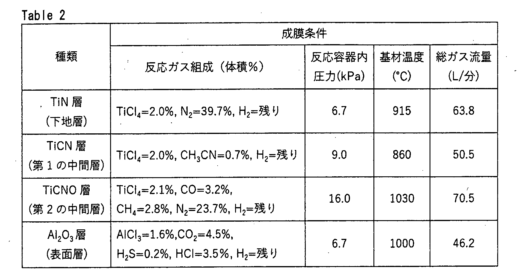
被膜中のTiSiCNの組成を有する層(以下、「TiSiCN層」とも記す。)は、表3の成膜条件A~成膜条件D、表4の成膜条件X及び成膜条件Yのいずれかで形成される。

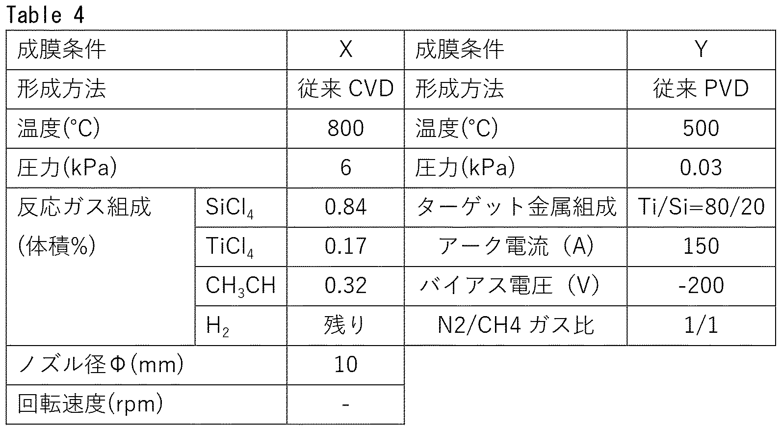
成膜条件A~成膜条件Dでは、図16に示されるCVD装置を用いてTiSiCN層(第1層)を形成する。CVD装置のノズルには、第1噴射孔、第2噴射孔(第2-1噴射孔及び第2-2噴射孔)及び第3噴射孔が設けられている。各成膜条件で用いられるCVD装置のノズルにおける第2-1噴射孔の径φr1及び第2-2噴射孔の径φr2を、表3の「噴射孔の径φ(mm)r1/r2」欄に示す。たとえば、成膜条件Aでは、第2-1噴射孔の径φr1は1.5mmであり、第2-2噴射孔の径φr2は2.5mmである。該ノズルは、成膜中に回転する。
成膜条件Xでは、従来のCVD装置を用いてTiSiCN層を形成する。CVD装置のノズルの噴射孔の径φは全て同一で、10mmである。該ノズルは、成膜中に回転しない。
成膜条件Yでは、従来のPVD法により第1層を形成する。成膜条件Yの具体的な条件は、表4の「成膜条件Y」の列に示す通りである。
次に、第2工程で形成された被膜に対して熱処理を行い、各試料の切削工具を得た。熱処理の条件は、表5の熱処理条件C1~熱処理条件C3に示される通りである。例えば、熱処理条件C1では、被膜を圧力900hPの水素(H2)雰囲気中で、1100℃で10分間加熱した。続いて、切削工具を冷却した。
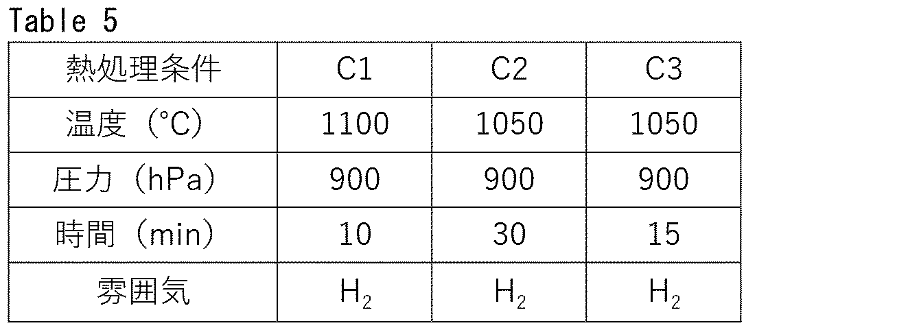
≪TiSiCN層の構造≫
成膜条件A~成膜条件Dを用いて形成されたTiSiCN層(第1層)は、複数の硬質粒子からなり、該硬質粒子は、立方晶型の結晶構造を有するTiSiCNからなり、該硬質粒子は、珪素の濃度が相対的に高い層と低い層とが交互に積層したラメラ構造を有することが確認された。さらに、珪素の濃度が相対的に高い層と低い層とは、同一の結晶方位を有することが確認された。具体的な確認方法は実施形態1に記載の通りであるため、その説明は繰り返さない。
各試料について、ラメラ構造における珪素高濃度層及び珪素低濃度層のそれぞれにおいて、百分率{XSi/(XSi+XTi)}×100を測定した。具体的な測定方法は実施形態1に記載の通りであるため、その説明は繰り返さない。結果を表7、表9、表11、表13、表15の「硬質粒子」の「珪素高濃度層」の「{XSi/(XSi+XTi)}×100(%)」欄、及び、「珪素低濃度層」の「{XSi/(XSi+XTi)}×100(%)」欄に示す。なお「-」の表記は、測定を行わなかったことを示す。
各試料について、硬質粒子の平均アスペクト比を測定した。具体的な測定方法は実施形態1に記載の通りであるため、その説明は繰り返さない。結果を表7、表9、表11、表13、表15の「硬質粒子」の「平均アスペクト比」欄に示す。
各試料のTiSiCN層(第1層)において、硬質粒子間の粒界領域における珪素の原子数ASi及びチタンの原子数ATiの合計に対する珪素の原子数ASiの百分率{ASi/(ASi+ATi)}×100の最大値、及び、第1層における珪素の原子数BSi及びチタンの原子数BTiの合計に対する珪素の原子数BSiの百分率{BSi/(BSi+BTi)}×100の平均値を測定した。具体的な測定方法は実施形態1に記載の通りであるため、その説明は繰り返さない。結果を表7、表9、表11、表13、表15の「粒界領域」の「{ASi/(ASi+ATi)}×100 最大値」欄、及び、「第1層」の「{BSi/(BSi+BTi)}×100 平均値」欄に示す。
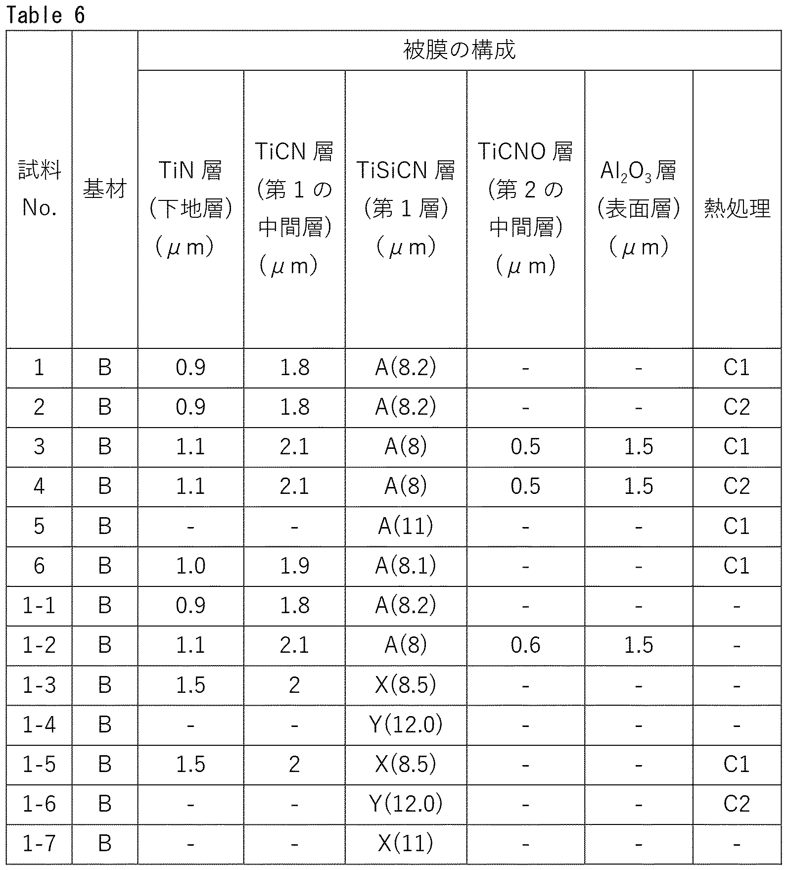


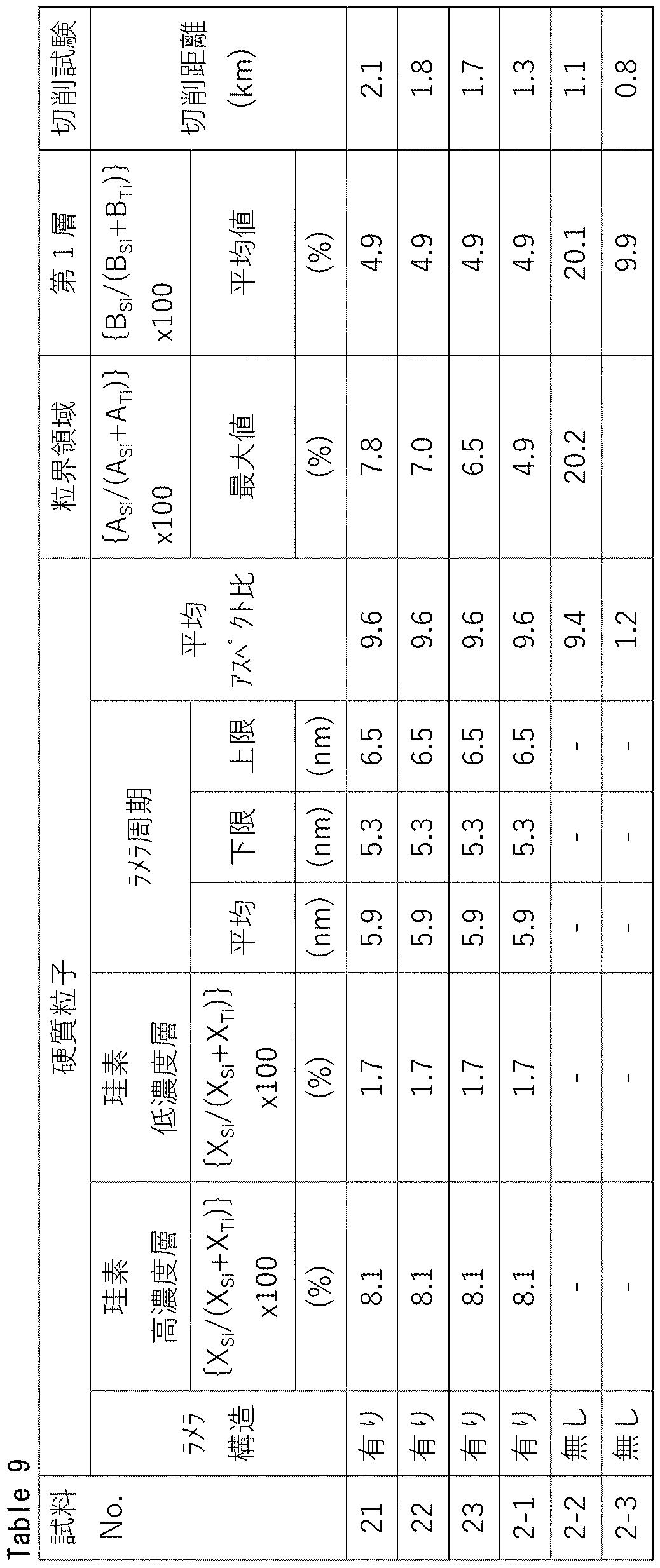
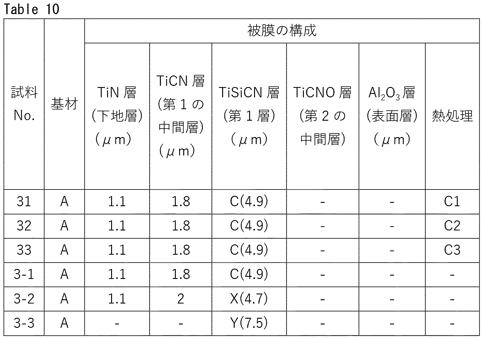

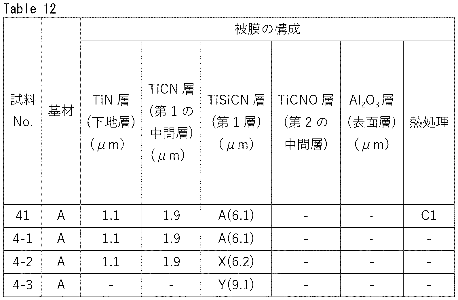
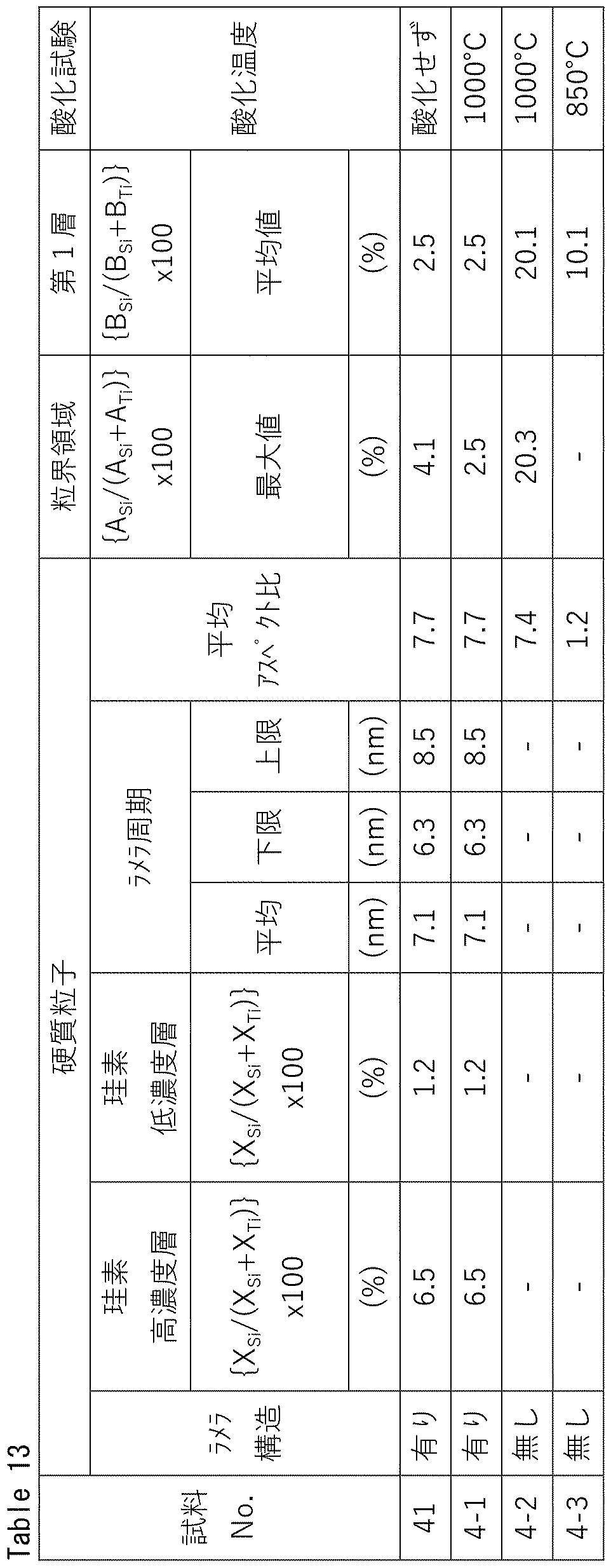

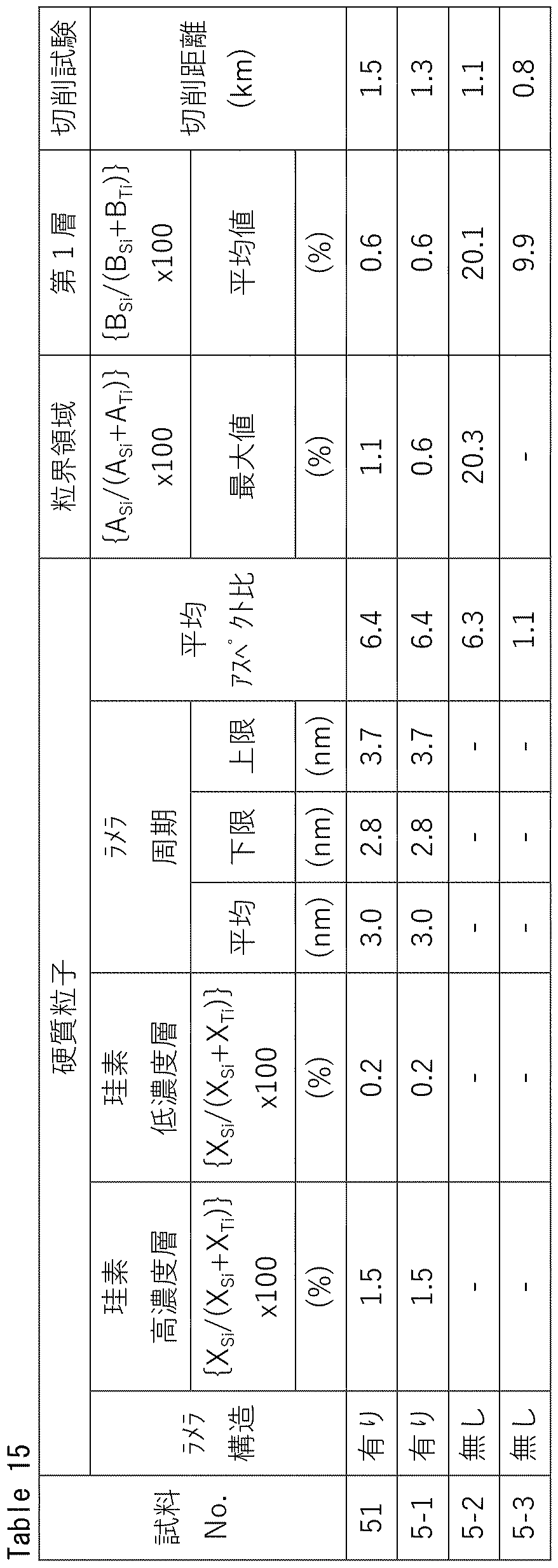
試料1~試料6(実施例)及び試料1-1~1-7(比較例)の切削工具を用いて、以下の切削条件にて切削を行い、工具刃先が欠損状態となるまでの切削距離を測定した。以下の切削条件は、一般鋼の旋削加工であり、高能率加工に該当する。切削距離が長いもの程、工具寿命が長いことを示す。結果を表7の「切削試験」の「切削距離(km)」欄に示す。
被削材:SUJ2 (形状:棒材 φ260mm×1000mm)
ホルダー:DCLNR2525M12
インサート:CMNG120408N-GU
切削速度Vc:300m/min
切り込み深さap:1.5mm
送り量f:0.3mm
切削液:あり(Wet)
試料1~試料6の切削工具は実施例に該当し、試料1-1~試料1-7の切削工具は比較例に該当する。試料1~試料6の切削工具は、試料1-1~試料1-7の切削工具よりも、高能率加工において工具寿命が長いことが確認された。これは、硬質粒子がラメラ構造を有しているため、被膜の耐熱亀裂伝搬性及び耐剥離性が向上し、更に、粒界領域に珪素が濃化していることで硬質粒子および/または基材の酸化が抑制され、耐摩耗性が向上したためと推察される。
試料21~試料23(実施例)及び試料2-1~試料2-3(比較例)の切削工具を用いて、以下の切削条件にて切削を行い、工具刃先が欠損状態となるまでの切削距離を測定した。以下の切削条件は、鋳鉄の旋削加工であり、高能率加工に該当する。切削距離が長いもの程、工具寿命が長いことを示す。結果を表9の「切削試験」の「切削距離(km)」欄に示す。
被削材:FCD700 (形状:棒材 φ260mm×1000mm)
ホルダー:DCLNR2525M12
インサート:CMNG120408N-GZ
切削速度Vc:140m/min
切り込み深さap:1.5mm
送り量f:0.3mm
切削液:あり(Wet)
試料21~試料23(実施例)は、試料2-1~試料2-3(比較例)に比べて、鋳鉄の旋削加工において切削距離が長く、高能率加工において工具寿命が長いことが確認された。これは、試料21~試料23では、粒界領域に珪素が濃化していることで硬質粒子および/または基材の酸化が抑制され、耐摩耗性が向上したためと推察される。
試料31~試料33(実施例)及び試料3-1~試料3-3(比較例)の切削工具を用いて、以下の切削条件にて切削を行い、工具刃先が欠損状態となるまでの切削距離を測定した。以下の切削条件は、一般鋼のフライス加工であり、高能率加工に該当する。切削距離が長いもの程、工具寿命が長いことを示す。結果を表11の「切削試験」の「切削距離(km)」欄に示す。
被削材:S50Cブロック材
カッター:DFC09100RS(住友電工ハードメタル社製)
インサート:XNMU060608PNER-G
切削速度Vc:200m/min
1刃当たりの送り量fz:0.2mm/t
切り込み深さap:3.0mm
切削幅ae:85mm
切削液:なし(Dry)
試料31~試料33(実施例)は、試料3-1~試料3-3(比較例)に比べて、一般鋼のフライス加工において切削距離が長く、高能率加工において工具寿命が長いことが確認された。これは、試料31~試料33では、粒界領域に珪素が濃化していることで硬質粒子および/または基材の酸化が抑制され、耐摩耗性が向上したためと推察される。
試料41(実施例)及び試料4-1~試料4-3(比較例)の切削工具を用いて、耐酸化性試験を行った。耐酸化性試験は以下の手順で行った。
試料41(実施例)は、1000℃に加熱しても酸化しないことが確認された。これは、試料41では、粒界の珪素(Si)が、酸素(O)が粒界に沿って拡散するのを抑制し、耐酸化性が向上したためと推察される。
試料51(実施例)及び試料5-1~試料5-3(比較例)の切削工具を用いて、以下の切削条件にて切削を行い、工具刃先が欠損状態となるまでの切削距離を測定した。以下の切削条件は、一般鋼のフライス加工であり、高能率加工に該当する。切削距離が長いもの程、工具寿命が長いことを示す。結果を表15の「切削試験」の「切削距離(km)」欄に示す。
被削材:SCM435フライス(85mm×100mm×300mm)
カッター:WGC4160R(住友電工ハードメタル社製)
インサート:SEET13T3AGSN-G
切削速度Vc:350m/min
1刃当たりの送り量fz:0.2mm/t
切り込み深さap:2.0mm
切削幅ae:85mm
切削液:なし(Dry)
試料51(実施例)は、試料5-1~試料5-2(比較例)に比べて、一般鋼のフライス加工において切削距離が長く、高能率加工において工具寿命が長いことが確認された。これは、試料51では、粒界領域に珪素が濃化していることで硬質粒子および/または基材の酸化が抑制され、耐摩耗性が向上したためと推察される。
今回開示された実施の形態および実施例はすべての点で例示であって、制限的なものではないと考えられるべきである。本発明の範囲は上記した実施の形態および実施例ではなく請求の範囲によって示され、請求の範囲と均等の意味、および範囲内でのすべての変更が含まれることが意図される。
Claims (9)
- 基材と、前記基材上に配置された被膜とを含む切削工具であって、
前記被膜は、複数の硬質粒子からなる第1層を備え、
前記硬質粒子は、立方晶型の結晶構造を有するTiSiCNからなり、
前記硬質粒子は、珪素の濃度が相対的に高い層と低い層とが交互に積層したラメラ構造を有し、
前記硬質粒子間の粒界領域における珪素の原子数ASi及びチタンの原子数ATiの合計に対する前記珪素の原子数ASiの百分率{ASi/(ASi+ATi)}×100の最大値は、前記第1層における珪素の原子数BSi及びチタンの原子数BTiの合計に対する前記珪素の原子数BSiの百分率{BSi/(BSi+BTi)}×100の平均値よりも大きい、
切削工具。 - 前記百分率{ASi/(ASi+ATi)}×100の最大値と、前記百分率{BSi/(BSi+BTi)}×100の平均値との差は、0.5%以上である、請求項1に記載の切削工具。
- 前記百分率{BSi/(BSi+BTi)}×100の平均値は、0.5%以上10%以下である、請求項1又は請求項2に記載の切削工具。
- 前記第1層の厚さは、3μm以上15μm以下であり、
前記被膜の厚さは、3μm以上30μm以下である、請求項1から請求項3のいずれか1項に記載の切削工具。 - 前記百分率{ASi/(ASi+ATi)}×100の最大値は、STEM-EDXを用いて、前記被膜表面の法線に沿う断面において、前記粒界領域に対して、前記粒界領域の伸長方向に垂直な方向に、長さ60nm以上のライン分析を行うことにより測定され、
前記百分率{BSi/(BSi+BTi)}×100の平均値は、STEM-EDXを用いて、前記断面において、前記第1層中に設けられた100nm×100nmの矩形の測定視野に対して矩形分析を行うことにより測定される、請求項1から請求項4のいずれか1項に記載の切削工具。 - 前記硬質粒子の平均アスペクト比は2以上である、請求項1から請求項5のいずれか1項に記載の切削工具。
- 請求項1から請求項6のいずれか1項に記載の切削工具の製造方法であって、
基材を準備する第1工程と、
前記基材上に被膜を形成する第2工程と、
前記被膜に対して熱処理を行い切削工具を得る第3工程と、を備え、
前記第2工程で形成される被膜は、複数の硬質粒子からなる第1層を備え、
前記硬質粒子は、立方晶型の結晶構造を有するTiSiCNからなり、
前記硬質粒子は、珪素の濃度が相対的に高い層と低い層とが交互に積層したラメラ構造を有する、切削工具の製造方法。 - 前記第3工程における熱処理は、前記被膜を圧力850hPa以上950hPa以下の水素雰囲気中で、1050℃以上1100℃以下で5分以上30分以下加熱する工程を含む、請求項7に記載の切削工具の製造方法。
- 前記第2工程は、CVD装置を用いたCVD法により前記第1層を形成する第2a工程を含み、
前記第2a工程は、TiCl4ガス、SiCl4ガス及びCH3CNガスを前記基材の表面に向かって噴出する第2a-1工程を含み、
前記TiCl4ガスは、前記CVD装置のノズルに設けられた複数の第1噴射孔から噴出され、
前記SiCl4ガスは、前記ノズルに設けられた複数の第2噴射孔から噴出され、
前記CH3CNガスは、前記ノズルに設けられた複数の第3噴射孔から噴出され、
前記第2a-1工程において、前記ノズルは回転し、
前記複数の第2噴射孔は、第2-1噴射孔と、第2-2噴射孔と、を含み、
前記第2-1噴射孔の径r1は、前記第2-2噴射孔の径r2と異なる、請求項7又は請求項8に記載の切削工具の製造方法。
Priority Applications (5)
| Application Number | Priority Date | Filing Date | Title |
|---|---|---|---|
| JP2022530208A JP7332048B1 (ja) | 2022-01-25 | 2022-01-25 | 切削工具及びその製造方法 |
| PCT/JP2022/002579 WO2023144867A1 (ja) | 2022-01-25 | 2022-01-25 | 切削工具及びその製造方法 |
| CN202280028944.2A CN117203010B (zh) | 2022-01-25 | 2022-01-25 | 切削工具及其制造方法 |
| EP22923736.7A EP4292736B1 (en) | 2022-01-25 | 2022-01-25 | Cutting tool and method for manufacturing same |
| US17/794,989 US11786975B2 (en) | 2022-01-25 | 2022-01-25 | Cutting tool and method for manufacturing the same |
Applications Claiming Priority (1)
| Application Number | Priority Date | Filing Date | Title |
|---|---|---|---|
| PCT/JP2022/002579 WO2023144867A1 (ja) | 2022-01-25 | 2022-01-25 | 切削工具及びその製造方法 |
Publications (1)
| Publication Number | Publication Date |
|---|---|
| WO2023144867A1 true WO2023144867A1 (ja) | 2023-08-03 |
Family
ID=87313289
Family Applications (1)
| Application Number | Title | Priority Date | Filing Date |
|---|---|---|---|
| PCT/JP2022/002579 Ceased WO2023144867A1 (ja) | 2022-01-25 | 2022-01-25 | 切削工具及びその製造方法 |
Country Status (5)
| Country | Link |
|---|---|
| US (1) | US11786975B2 (ja) |
| EP (1) | EP4292736B1 (ja) |
| JP (1) | JP7332048B1 (ja) |
| CN (1) | CN117203010B (ja) |
| WO (1) | WO2023144867A1 (ja) |
Cited By (2)
| Publication number | Priority date | Publication date | Assignee | Title |
|---|---|---|---|---|
| JP7729493B1 (ja) * | 2024-05-29 | 2025-08-26 | 住友電気工業株式会社 | 切削工具 |
| JP7729494B1 (ja) * | 2024-05-29 | 2025-08-26 | 住友電気工業株式会社 | 切削工具 |
Families Citing this family (1)
| Publication number | Priority date | Publication date | Assignee | Title |
|---|---|---|---|---|
| EP4575034A4 (en) * | 2023-07-13 | 2025-06-25 | Sumitomo Electric Industries, Ltd. | CUTTING TOOL |
Citations (4)
| Publication number | Priority date | Publication date | Assignee | Title |
|---|---|---|---|---|
| JP2015505902A (ja) | 2011-12-05 | 2015-02-26 | フラウンホーファー−ゲゼルシャフト ツル フェルデルング デル アンゲヴァンテン フォルシュング エー ファウFraunhofer−Gesellschaft zur Foerderung der angewandten Forschung e.V. | 金属、硬質金属、サーメット又はセラミックの硬質材料被覆体並びにこのような物体の製造法 |
| JP2019171547A (ja) * | 2018-03-29 | 2019-10-10 | 住友電工ハードメタル株式会社 | 表面被覆切削工具及びその製造方法 |
| JP2020507679A (ja) | 2017-02-10 | 2020-03-12 | フラウンホーファー−ゲゼルシャフト ツル フェルデルング デル アンゲヴァンテン フォルシュング エー ファウFraunhofer−Gesellschaft zur Foerderung der angewandten Forschung e.V. | 金属、超硬合金、サーメット、またはセラミックスからなる硬質材コーティング体、および該物体の製造方法 |
| CN113529016A (zh) * | 2021-09-16 | 2021-10-22 | 山东天瑞重工有限公司 | TiSiCN纳米涂层及其制备方法以及活塞 |
Family Cites Families (12)
| Publication number | Priority date | Publication date | Assignee | Title |
|---|---|---|---|---|
| JP2004090150A (ja) * | 2002-08-30 | 2004-03-25 | Sumitomo Electric Ind Ltd | 表面被覆切削工具 |
| JP4398224B2 (ja) * | 2003-11-05 | 2010-01-13 | 住友電工ハードメタル株式会社 | 耐摩耗性部材 |
| KR20100015344A (ko) * | 2007-04-18 | 2010-02-12 | 산드빅 인터렉츄얼 프로퍼티 에이비 | 코팅된 절삭 공구 및 이의 제조 방법 |
| JP2009220239A (ja) * | 2008-03-18 | 2009-10-01 | Mitsubishi Materials Corp | 硬質被覆層がすぐれた耐欠損性を発揮する表面被覆切削工具 |
| CN102066617B (zh) * | 2008-04-18 | 2014-04-02 | 山特维克知识产权股份有限公司 | 涂层切削工具和其制造方法 |
| KR102056206B1 (ko) * | 2012-10-01 | 2019-12-16 | 미츠비시 히타치 쓰루 가부시키가이샤 | 경질 피막 피복 공구 및 그 제조 방법 |
| CN104789938A (zh) * | 2014-01-22 | 2015-07-22 | 三菱综合材料株式会社 | 硬质包覆层发挥优异的耐崩刀性的表面包覆切削工具 |
| CN104087898B (zh) * | 2014-07-18 | 2017-05-03 | 上海理工大学 | 一种具有超高硬度、低摩擦系数的TiSiCN纳米复合涂层及制备方法 |
| JP6284034B2 (ja) * | 2014-09-25 | 2018-02-28 | 三菱マテリアル株式会社 | 硬質被覆層がすぐれた耐チッピング性を発揮する表面被覆切削工具 |
| US11220760B2 (en) * | 2016-04-14 | 2022-01-11 | Sumitomo Electric Hardmetal Corp. | Surface-coated cutting tool and method of producing the same |
| JP6973699B2 (ja) * | 2016-04-14 | 2021-12-01 | 住友電工ハードメタル株式会社 | 表面被覆切削工具およびその製造方法 |
| JP6635340B2 (ja) * | 2016-08-24 | 2020-01-22 | 住友電工ハードメタル株式会社 | 表面被覆切削工具およびその製造方法 |
-
2022
- 2022-01-25 JP JP2022530208A patent/JP7332048B1/ja active Active
- 2022-01-25 EP EP22923736.7A patent/EP4292736B1/en active Active
- 2022-01-25 US US17/794,989 patent/US11786975B2/en active Active
- 2022-01-25 CN CN202280028944.2A patent/CN117203010B/zh active Active
- 2022-01-25 WO PCT/JP2022/002579 patent/WO2023144867A1/ja not_active Ceased
Patent Citations (4)
| Publication number | Priority date | Publication date | Assignee | Title |
|---|---|---|---|---|
| JP2015505902A (ja) | 2011-12-05 | 2015-02-26 | フラウンホーファー−ゲゼルシャフト ツル フェルデルング デル アンゲヴァンテン フォルシュング エー ファウFraunhofer−Gesellschaft zur Foerderung der angewandten Forschung e.V. | 金属、硬質金属、サーメット又はセラミックの硬質材料被覆体並びにこのような物体の製造法 |
| JP2020507679A (ja) | 2017-02-10 | 2020-03-12 | フラウンホーファー−ゲゼルシャフト ツル フェルデルング デル アンゲヴァンテン フォルシュング エー ファウFraunhofer−Gesellschaft zur Foerderung der angewandten Forschung e.V. | 金属、超硬合金、サーメット、またはセラミックスからなる硬質材コーティング体、および該物体の製造方法 |
| JP2019171547A (ja) * | 2018-03-29 | 2019-10-10 | 住友電工ハードメタル株式会社 | 表面被覆切削工具及びその製造方法 |
| CN113529016A (zh) * | 2021-09-16 | 2021-10-22 | 山东天瑞重工有限公司 | TiSiCN纳米涂层及其制备方法以及活塞 |
Non-Patent Citations (2)
| Title |
|---|
| See also references of EP4292736A4 |
| SHINYA IMAMURA ET AL.: "Properties and cutting performance of AlTiCrN/TiSiCN bilayer coatings deposited by cathodic-arc ion plating", SURFACE AND COATINGS TECHNOLOGY, vol. 202, 2007, pages 820 - 825, XP022342021, DOI: 10.1016/j.surfcoat.2007.05.087 |
Cited By (5)
| Publication number | Priority date | Publication date | Assignee | Title |
|---|---|---|---|---|
| JP7729493B1 (ja) * | 2024-05-29 | 2025-08-26 | 住友電気工業株式会社 | 切削工具 |
| JP7729494B1 (ja) * | 2024-05-29 | 2025-08-26 | 住友電気工業株式会社 | 切削工具 |
| US12454010B1 (en) | 2024-05-29 | 2025-10-28 | Sumitomo Electric Industries, Ltd. | Cutting tool |
| WO2025248670A1 (ja) * | 2024-05-29 | 2025-12-04 | 住友電気工業株式会社 | 切削工具 |
| WO2025248671A1 (ja) * | 2024-05-29 | 2025-12-04 | 住友電気工業株式会社 | 切削工具 |
Also Published As
| Publication number | Publication date |
|---|---|
| EP4292736A1 (en) | 2023-12-20 |
| CN117203010B (zh) | 2024-06-07 |
| CN117203010A (zh) | 2023-12-08 |
| EP4292736A4 (en) | 2024-05-29 |
| JPWO2023144867A1 (ja) | 2023-08-03 |
| US11786975B2 (en) | 2023-10-17 |
| JP7332048B1 (ja) | 2023-08-23 |
| US20230234141A1 (en) | 2023-07-27 |
| EP4292736B1 (en) | 2026-03-11 |
Similar Documents
| Publication | Publication Date | Title |
|---|---|---|
| JP7332048B1 (ja) | 切削工具及びその製造方法 | |
| JP7517600B2 (ja) | 切削工具 | |
| JP7568076B2 (ja) | 切削工具及びその製造方法 | |
| JP7529147B2 (ja) | 切削工具 | |
| EP3008225A1 (en) | Coated cutting tool | |
| JP7416327B1 (ja) | 切削工具 | |
| JP7416328B1 (ja) | 切削工具 | |
| JP7533347B2 (ja) | 切削工具 | |
| JP7559981B1 (ja) | 切削工具 | |
| JP7559979B1 (ja) | 切削工具 | |
| JP7729494B1 (ja) | 切削工具 | |
| JP7517599B2 (ja) | 切削工具 | |
| JP7124236B1 (ja) | 切削工具 | |
| JP7543975B2 (ja) | 切削工具 | |
| JP7533345B2 (ja) | 切削工具 | |
| JP7533346B2 (ja) | 切削工具 | |
| JP7533344B2 (ja) | 切削工具 | |
| WO2025248670A1 (ja) | 切削工具 | |
| JP2024138692A (ja) | 表面被覆切削工具 | |
| WO2022264196A1 (ja) | 切削工具 |
Legal Events
| Date | Code | Title | Description |
|---|---|---|---|
| WWE | Wipo information: entry into national phase |
Ref document number: 2022530208 Country of ref document: JP |
|
| 121 | Ep: the epo has been informed by wipo that ep was designated in this application |
Ref document number: 22923736 Country of ref document: EP Kind code of ref document: A1 |
|
| WWE | Wipo information: entry into national phase |
Ref document number: 2022923736 Country of ref document: EP |
|
| ENP | Entry into the national phase |
Ref document number: 2022923736 Country of ref document: EP Effective date: 20230915 |
|
| WWE | Wipo information: entry into national phase |
Ref document number: 202280028944.2 Country of ref document: CN |
|
| NENP | Non-entry into the national phase |
Ref country code: DE |
|
| WWG | Wipo information: grant in national office |
Ref document number: 2022923736 Country of ref document: EP |