WO2023149060A1 - 測定装置 - Google Patents
測定装置 Download PDFInfo
- Publication number
- WO2023149060A1 WO2023149060A1 PCT/JP2022/043371 JP2022043371W WO2023149060A1 WO 2023149060 A1 WO2023149060 A1 WO 2023149060A1 JP 2022043371 W JP2022043371 W JP 2022043371W WO 2023149060 A1 WO2023149060 A1 WO 2023149060A1
- Authority
- WO
- WIPO (PCT)
- Prior art keywords
- exposure
- sub
- light
- period
- imaging sensor
- Prior art date
- Legal status (The legal status is an assumption and is not a legal conclusion. Google has not performed a legal analysis and makes no representation as to the accuracy of the status listed.)
- Ceased
Links
Images


Classifications
-
- G—PHYSICS
- G01—MEASURING; TESTING
- G01S—RADIO DIRECTION-FINDING; RADIO NAVIGATION; DETERMINING DISTANCE OR VELOCITY BY USE OF RADIO WAVES; LOCATING OR PRESENCE-DETECTING BY USE OF THE REFLECTION OR RERADIATION OF RADIO WAVES; ANALOGOUS ARRANGEMENTS USING OTHER WAVES
- G01S7/00—Details of systems according to groups G01S13/00, G01S15/00, G01S17/00
- G01S7/48—Details of systems according to groups G01S13/00, G01S15/00, G01S17/00 of systems according to group G01S17/00
- G01S7/483—Details of pulse systems
- G01S7/486—Receivers
- G01S7/4868—Controlling received signal intensity or exposure of sensor
-
- G—PHYSICS
- G01—MEASURING; TESTING
- G01S—RADIO DIRECTION-FINDING; RADIO NAVIGATION; DETERMINING DISTANCE OR VELOCITY BY USE OF RADIO WAVES; LOCATING OR PRESENCE-DETECTING BY USE OF THE REFLECTION OR RERADIATION OF RADIO WAVES; ANALOGOUS ARRANGEMENTS USING OTHER WAVES
- G01S17/00—Systems using the reflection or reradiation of electromagnetic waves other than radio waves, e.g. lidar systems
- G01S17/02—Systems using the reflection of electromagnetic waves other than radio waves
- G01S17/06—Systems determining position data of a target
- G01S17/08—Systems determining position data of a target for measuring distance only
- G01S17/10—Systems determining position data of a target for measuring distance only using transmission of interrupted, pulse-modulated waves
-
- G—PHYSICS
- G01—MEASURING; TESTING
- G01S—RADIO DIRECTION-FINDING; RADIO NAVIGATION; DETERMINING DISTANCE OR VELOCITY BY USE OF RADIO WAVES; LOCATING OR PRESENCE-DETECTING BY USE OF THE REFLECTION OR RERADIATION OF RADIO WAVES; ANALOGOUS ARRANGEMENTS USING OTHER WAVES
- G01S17/00—Systems using the reflection or reradiation of electromagnetic waves other than radio waves, e.g. lidar systems
- G01S17/88—Lidar systems specially adapted for specific applications
- G01S17/89—Lidar systems specially adapted for specific applications for mapping or imaging
- G01S17/894—Three-dimensional [3D] imaging with simultaneous measurement of time-of-flight at a two-dimensional [2D] array of receiver pixels, e.g. time-of-flight cameras or flash lidar
-
- G—PHYSICS
- G01—MEASURING; TESTING
- G01S—RADIO DIRECTION-FINDING; RADIO NAVIGATION; DETERMINING DISTANCE OR VELOCITY BY USE OF RADIO WAVES; LOCATING OR PRESENCE-DETECTING BY USE OF THE REFLECTION OR RERADIATION OF RADIO WAVES; ANALOGOUS ARRANGEMENTS USING OTHER WAVES
- G01S7/00—Details of systems according to groups G01S13/00, G01S15/00, G01S17/00
- G01S7/48—Details of systems according to groups G01S13/00, G01S15/00, G01S17/00 of systems according to group G01S17/00
- G01S7/483—Details of pulse systems
- G01S7/486—Receivers
- G01S7/4861—Circuits for detection, sampling, integration or read-out
- G01S7/4863—Detector arrays, e.g. charge-transfer gates
-
- G—PHYSICS
- G01—MEASURING; TESTING
- G01S—RADIO DIRECTION-FINDING; RADIO NAVIGATION; DETERMINING DISTANCE OR VELOCITY BY USE OF RADIO WAVES; LOCATING OR PRESENCE-DETECTING BY USE OF THE REFLECTION OR RERADIATION OF RADIO WAVES; ANALOGOUS ARRANGEMENTS USING OTHER WAVES
- G01S7/00—Details of systems according to groups G01S13/00, G01S15/00, G01S17/00
- G01S7/48—Details of systems according to groups G01S13/00, G01S15/00, G01S17/00 of systems according to group G01S17/00
- G01S7/483—Details of pulse systems
- G01S7/486—Receivers
- G01S7/4865—Time delay measurement, e.g. time-of-flight measurement, time of arrival measurement or determining the exact position of a peak
Definitions
- the present disclosure relates to measuring devices.
- Patent Document 1 discloses an indirect ToF (Time of Flight) measuring device that measures the distance to an object based on irradiation with laser light (pulse light) and exposure of the reflected light. are doing.
- ToF Time of Flight
- the measuring device of Patent Document 1 exposure is performed with the same width as the pulse width of the emitted light.
- the depth of the area to be measured can be increased, and as a result, the frame rate (FPS) can be increased.
- the light emission pulse width is often limited to a certain range, and if the exposure period is extended beyond that range, the light emission pulse width ⁇ exposure width. Even in this case, the depth of the measurement target area can be increased and the speed can be increased. end up For this reason, it is difficult to increase the frame rate under the condition of light emission pulse width ⁇ exposure width.
- An object of the present disclosure is to increase the frame rate even under the condition of light emission pulse width ⁇ exposure width.
- a measuring device for achieving the above object, a light emitting unit that emits pulsed light; an imaging sensor that outputs a signal value corresponding to the amount of exposure for each pixel; a timing control unit that sets an exposure period corresponding to an area to be measured and exposes the pixels of the imaging sensor to reflected light during the exposure period; a signal acquisition unit that acquires a signal value corresponding to the exposure amount of the pixel in the exposure period based on the output of the imaging sensor;
- the timing control unit is configured to set, as the exposure period, a plurality of sub-exposure periods longer than the width of the pulsed light and having different start timings so as to have overlapping periods corresponding to the width of the pulsed light.
- the signal acquisition unit acquires the signal value corresponding to the sum of the exposure amounts of the pixels in the plurality of sub-exposure periods.
- FIG. 1A is an explanatory view of the configuration of the measuring device 1.
- FIG. 1B is an explanatory diagram of light emission timing and exposure timing.
- FIG. 2 is an explanatory diagram of distance image creation by indirect ToF.
- FIG. 3A is an explanatory diagram of the normal mode.
- FIG. 3B is an explanatory diagram of the high speed mode.
- FIG. 4A is an explanatory diagram of the light emitting operation and the exposure operation in the normal mode, and is an explanatory diagram when the arrival time of the reflected light is earlier than the exposure start timing (delay time Tdelay).
- FIG. 4B is an explanatory diagram of the light emitting operation and the exposure operation in the normal mode, and is an explanatory diagram when the arrival time of the reflected light coincides with the exposure start timing (delay time Tdelay).
- FIG. 4C is an explanatory diagram of the light emitting operation and the exposure operation in the normal mode, and is an explanatory diagram when the arrival time of the reflected light is later than the exposure start timing (delay time Tdelay).
- FIG. 5 is an explanatory diagram of the relationship between the distance to the object and the amount of exposure in the normal mode.
- FIG. 6A is an explanatory diagram of the relationship between the light emission operation and the exposure operation in the normal mode.
- FIG. 6B is a diagram showing the relationship between the exposure amounts and the distances of the exposure operations A and B in FIG. 6A.
- FIG. 7A is an explanatory diagram of processing in the high-speed mode, and is an explanatory diagram when the arrival time of the reflected light coincides with the exposure start timing (delay time Tdelay).
- FIG. 7B is an explanatory diagram of processing in the high-speed mode, and is an explanatory diagram when the arrival time of the reflected light is later than the exposure start timing (delay time Tdelay).
- FIG. 8 is an explanatory diagram of the relationship between the distance to the object and the amount of exposure in high-speed mode.
- FIG. 9A is a timing chart of light emitting operation and exposure operation in high speed mode.
- FIG. 9B is an explanatory diagram of the relationship between the distance to the object and the amount of exposure.
- FIG. 10 is a diagram showing a configuration example of the imaging sensor 22 with 4 taps.
- FIG. 11A is a timing chart of light emitting operation and light receiving operation in the normal mode when the imaging sensor 22 with 4 taps is used.
- FIG. 11B is an explanatory diagram of the relationship between the distance to the object and the amount of exposure.
- FIG. 12A is a timing chart of light emitting operation and light receiving operation in high-speed mode when the imaging sensor 22 with 4 taps is used.
- FIG. 12B is an explanatory diagram of the relationship between the distance to the object and the amount of exposure.
- FIG. 13 is a diagram for explaining alternately performing sub-exposure operations (sub-exposure periods).
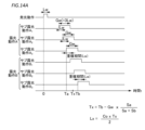
- FIG. 14A is a timing chart of light emission operation and exposure operation when there are three sub-exposure operations.
- FIG. 14B is an explanatory diagram of the relationship between the distance and the exposure amount when there
- FIG. 1A is an explanatory view of the configuration of the measuring device 1.
- FIG. A measuring device 1 illustrated in FIG. 1A is a ToF (Time of Flight) type device that measures the distance to an object in front. In this embodiment, an indirect ToF camera is used. With such a measuring device 1, the effects of fog and rain can be removed, and photography and measurement are possible even in bad weather.
- the measuring device 1 is provided, for example, in a vehicle.
- the measuring device 1 includes a light emitting section 10, an imaging section 20, and a control section 30.
- the light emitting unit 10 irradiates (projects) light onto the space to be photographed.
- the light emitting unit 10 emits light according to instructions from the control unit 30 .
- the light emitting unit 10 has a light source 12 and a light projecting optical system (not shown) that emits the light emitted by the light source 12 .
- the light source 12 is a light source having a light emitting element.
- the light source 12 emits pulsed laser light under the control of the controller 30 .
- this pulsed light (pulsed light) is also referred to as light emission pulse.
- the imaging unit 20 (indirect ToF camera) performs imaging based on exposing the light reflected by the object for distance measurement.
- the imaging unit 20 has an imaging sensor 22 and an exposure optical system (not shown) that guides incident (exposed) light to the imaging sensor 22 .
- the imaging sensor 22 captures an image of an object to be captured according to an instruction from the control unit 30 and outputs image data obtained by the capturing to the image acquisition unit 34 of the control unit 30 .
- the value of each pixel (pixel data) that constitutes this image data indicates a signal value corresponding to the amount of exposure. Note that the imaging sensor 22 will be described later.
- the control unit 30 controls the measuring device 1.
- the control unit 30 is realized by a hardware configuration such as elements and circuits such as a memory and a CPU.
- the control unit 30 implements a predetermined function by having the CPU execute a program stored in the memory.
- the control unit 30 is not limited to being realized by software processing execution by a memory and a CPU.
- it may be realized by hardware such as ASIC and FPGA.
- FIG. 1A Various functions realized by the control unit 30 includes a timing control section 32 , an image acquisition section 34 , a time calculation section 36 and a distance calculation section 38 .
- the timing control section 32 controls the light emission timing of the light emitting section 10 and the exposure timing of the imaging section 20 . Light emission timing and exposure timing will be described later.
- the image acquisition unit 34 acquires image data from the imaging sensor 22 of the imaging unit 20 .
- the image acquisition unit 34 also has a memory (not shown) that stores acquired image data. Note that the image acquisition unit 34 corresponds to a "signal acquisition unit".
- the time calculation unit 36 calculates the arrival time (time of flight of light: ToF) from when the light emitting unit 10 emits light until the reflected light reaches the imaging sensor 22 .
- the time calculator 36 corresponds to a "calculator".
- the distance calculation unit 38 calculates the distance based on the light arrival time. As will be described later, the measuring device 1 can acquire a distance image by having the distance calculator 38 calculate the distance for each pixel.
- FIG. 1B is an explanatory diagram of light emission timing and exposure timing.
- FIG. 2 is an explanatory diagram of creating a distance image by indirect ToF.
- the control unit 30 causes the light emitting unit 10 to emit light pulses.
- the width of this light emission pulse (hereinafter referred to as pulse width) is Lw.
- the control unit 30 (timing control unit 32) exposes the imaging sensor 22 of the imaging unit 20 to reflected light after a time Tdelay has passed since the irradiation of the light emission pulse.
- the exposure period is set by the delay time Tdelay and the exposure width Gw.
- the delay time Tdelay is the time (delay time) from the irradiation of the light emission pulse to the start of the exposure period.
- the delay time Tdelay is set according to the distance to the area to be measured. That is, if the measurement device 1 sets a short time from when the light emitting unit 10 irradiates the light emitting pulse to when the imaging sensor 22 exposes, the image of the object (object that reflects light) in the short range can be obtained. can be obtained. Conversely, the measurement apparatus 1 can acquire an image of an object in a long distance area by setting a long time from when the light emitting unit 10 irradiates the light emitting pulse to when the imaging sensor 22 exposes.
- the exposure width Gw is the width of the exposure period (that is, the period from the start of exposure to the end of exposure).
- the width of the exposure period defines the length of the area to be measured in the measurement direction. Therefore, the shorter the exposure width Gw, the higher the distance resolution.
- different exposure periods are set according to the distance to the area to be measured. Although four regions are shown in FIG. 2 for simplification, the number N of regions is not limited to four in practice.
- Light emission and exposure are repeated multiple times at a cycle Tp illustrated in FIG. 1B. This is due to charge accumulation in the imaging sensor 22, which will be described later. Also, the farther the area to be measured is, the larger the number of repetitions n is set. This is because the farther the area, the weaker the reflected light.
- the object object that reflects light
- the image for each region is sometimes called a "range image”.
- the value (image data) of each pixel forming an image indicates a signal value corresponding to the amount of exposure.
- the number of range images (for example, 4) obtained in one shot is sometimes called a “subframe”.
- a plurality of areas (for example, four areas) measured in one shot may be called a "zone”.
- the measuring device 1 of the present embodiment acquires image data of a plurality of regions at different distances, and based on the acquired plurality of image data, creates a distance image showing the distance to the object. can be obtained.
- the range image is an image obtained by cutting out a part of the distance
- the image obtained by summing these is a composite image of the entire distance (corresponding to a general photographed image).
- distance information is calculated based on the pixel value information of the range image, and an image obtained by arranging the information for each pixel becomes the distance image.
- the term 'frame' refers to the time axis at that time. Therefore, a "frame" in a ToF camera includes an all-range composite image and a range image.
- the control unit 30 causes the light emitting unit 10 to emit light at a period Tp (see FIG. 1B), and controls the exposure timing of the imaging sensor 22 of the imaging unit 20 according to the light emission timing, Allow exposure.
- Tp a period of the imaging sensor 22 of the imaging unit 20
- Allow exposure a period of the imaging sensor 22 of the imaging unit 20
- Tp a period of the imaging sensor 22 of the imaging unit 20
- control unit 30 acquires an image of region 1.
- the timing control unit 32 causes the imaging sensor 22 of the imaging unit 20 to perform exposure for each pixel of the image in an exposure period delayed from the light emission timing.
- the timing control unit 32 causes the imaging sensor 22 of the imaging unit 20 to perform exposure repeatedly (n times) every period Tp, and accumulates electric charges in the storage unit CS (described later) of the imaging sensor 22 .
- the image acquisition unit 34 acquires signal values corresponding to charges accumulated in the imaging sensor 22 (accumulation unit CS). Then, the acquired image data of the area 1 is written in the image memory.
- control unit 30 acquires an image of the area 2 adjacent (continuous) to the area 1 in the measurement direction. Then, the control unit 30 writes the image data of the area 2 to the image memory of the image acquisition unit 34 .
- the delay time Tdelay with respect to the light emission timing in region 2 is set longer than in region 1 . Further, as described above, the number of repetitions (the number of charge accumulations) is set to increase as the area to be measured becomes farther.
- the measuring device 1 of this embodiment can measure in two modes, a normal mode and a high speed mode.
- Figures 3A and 3B are explanatory diagrams of the normal mode and the high-speed mode. 3A and 3B, the length in the measurement direction indicates the distance from the measuring device 1. FIG.
- Normal mode is a mode in which normal measurement (general measurement by indirect ToF) is performed.
- High-speed mode is a mode that performs measurements faster than normal mode.
- the depth of the area to be measured becomes wider than in the normal mode, and the speed can be increased by reducing the number of areas (the number of images acquired when creating the range image).
- FIGS. 4A to 4C are explanatory diagrams of the light emission operation and the exposure operation in the normal mode.
- FIG. 4A is an explanatory diagram when the arrival time of reflected light is earlier than the exposure start timing (delay time Tdelay).
- FIG. 4B is an explanatory diagram when the arrival time of reflected light coincides with the exposure start timing (delay time Tdelay).
- FIG. 4C is an explanatory diagram when the arrival time of reflected light is later than the exposure start timing (delay time Tdelay).
- the horizontal axis of the timing charts of FIGS. 4A to 4C indicates "time”.
- the width Gw of the exposure period in the normal mode is equal to the pulse width Lw of the light emission pulse. Furthermore, the pulse width of the reflected light is also Lw.
- the arrival time of the reflected light matches the delay time Tdelay. At this time, the arrival period of the reflected light coincides with the exposure period of the imaging sensor 22, and all the reflected light can be exposed to the imaging sensor 22, so the exposure peaks.
- the distance to the object is L1 (L1 ⁇ L2) as shown in FIG. 4A
- the overlap between the arrival period of the reflected light and the exposure period of the imaging sensor 22 increases as the distance from L1 to L2 (see FIG. 4B) approaches.
- the amount of exposure gradually increases.
- the distance to the object is L3 (L3>L2) as shown in FIG. 4C, the overlap between the arrival period of the reflected light and the exposure period of the image sensor 22 decreases as the distance from L2 to L3 increases. gradually decreases.
- FIG. 5 is an explanatory diagram of the relationship between the distance to the object and the amount of exposure in normal mode.
- the horizontal axis of the graph in FIG. 5 indicates “distance”, and the vertical axis indicates “exposure amount (signal value)", which corresponds to the shaded area of the exposure operation in FIGS. 4A to 4C.
- FIG. 6A is an explanatory diagram of the relationship between the light emitting operation and the exposure operation in the normal mode.
- FIG. 6B is a diagram showing the relationship between the exposure amounts and the distances of the exposure operations A and B in FIG. 6A.
- the horizontal axis of FIG. 6A indicates time, and the horizontal axis of FIG. 6B indicates distance.
- the hatched area of the light emission pulse in FIG. 6A represents the "exposure amount", and the exposure amount-distance relationship diagram in FIG. 6B shows this area on the vertical axis.
- the pulse width of the light emission pulse is Lw.
- the pulse width of the reflected light is also Lw.
- exposure operation A and exposure operation B are set.
- an exposure period (exposure period A) corresponding to a predetermined area (hereinafter also referred to as one area) is set.
- the delay time of the exposure period A with respect to the light emission start (time 0) of the light emission pulse is the delay time Ta (corresponding to Tdelay in FIG. 1B).
- the exposure period is a period in which the level of the exposure operation in FIG. 6A is high level (H level).
- an exposure period (exposure period B) corresponding to an area continuous in the measurement direction of the predetermined area (hereinafter also referred to as the other area) is set.
- the timing control unit 32 sets such exposure operation A and exposure operation B to expose each pixel of the imaging sensor 22 to the reflected light. Then, the image acquisition unit 34 acquires signal values (here, signal values Sa and Sb illustrated in FIG. 6B ) corresponding to the exposure amount from the imaging sensor 22 .
- the signal value Sa is a signal value corresponding to the exposure amount A when the distance to the object is Lx, and corresponds to the pixel value (pixel data) forming the image data (range image) of one region.
- the signal value Sb is a signal value corresponding to the exposure amount B when the distance to the object is Lx, and corresponds to the pixel value (pixel data) constituting the image data (range image) of the other area. do.
- Tx is the arrival time (time of flight of light: ToF) from when the light source 12 emits light (light emission pulse) until the reflected light reaches the imaging sensor 22 .
- the time calculator 36 calculates the arrival time Tx according to Equation (1).
- the distance Lx to the object is calculated based on the arrival time Tx.
- the light travels twice as long as the distance L during the arrival time Tx.
- Lx (Co ⁇ Tx)/2 (2) becomes.
- the distance calculator 38 calculates the distance Lx for each pixel according to the equation (2) using the arrival time Tx.
- the ratio of the signal value Sa corresponding to the exposure amount A to the total signal value (Sa+Sb) changes according to the change in the distance Lx (arrival time Tx). Then, by having this relationship, the equation (1) is derived using the ratio of the signal value Sa. That is, the calculation of the arrival time Tx in the normal mode utilizes the triangular shape of the graph showing the relationship between the distance and the exposure amount.
- FIGS. 7A and 7B are explanatory diagrams of the processing in high speed mode.
- FIG. 7A is an explanatory diagram when the arrival time of reflected light coincides with the exposure start timing (delay time Tdelay).
- FIG. 7B is an explanatory diagram when the arrival time of reflected light is later than the exposure start timing (delay time Tdelay). In FIG. 7B, the arrival completion time of the reflected light coincides with the exposure end timing.
- the horizontal axis of the timing charts of FIGS. 7A and 7B indicates time.
- the arrival period of the reflected light is equal to the exposure of the imaging sensor 22 both when the distance to the object is L2 (FIG. 7A) and when the distance to the object is L2′ (FIG. 7B). Since it is included in the period, the imaging sensor 22 exposes all the reflected light. That is, the exposure amount is the same when the distance to the object is L2 and when the distance to the object is L2'.
- FIG. 8 is an explanatory diagram of the relationship between the distance to the object and the amount of exposure in high-speed mode. Note that the horizontal axis of the graph in FIG. 8 indicates "distance”.
- the exposure width Gw is set to be larger than the pulse width Lw of the light emission pulse (Gw>Lw). The amount becomes constant, and the graph showing the relationship between distance and exposure becomes "trapezoidal".
- the exposure amount does not change over the distances L2 to L2' (that is, the range of distances L2 to L2' becomes a dead zone). Therefore, simply setting the exposure width Gw long for the high-speed mode does not allow calculation of the arrival time Tx and the distance Lx by the indirect ToF as in the normal mode.
- it is difficult to change the pulse width Lw of the emitted light due to structural and cost constraints of the light source. For example, since heat is concentrated locally (on the time axis) during light emission, it is necessary to define the light emission duty and the light emission pulse width. Therefore, it is difficult to extend (change) the light emission pulse width Lw.
- FIG. 9A is a timing chart of light emission operation and exposure operation in high speed mode.
- FIG. 9B is an explanatory diagram of the relationship between the distance to the object and the amount of exposure.
- the horizontal axis of FIG. 9A indicates “time”, and the horizontal axis of FIG. 9B indicates "distance”.
- the timing control unit 32 of the control unit 30 of the present embodiment performs a plurality of (here, two) sub-exposure operations (sub-exposure operations) longer than the pulse width Lw as exposure operations (exposure periods). period). More specifically, the timing control unit 32 sets two sub-exposure operations (sub-exposure periods) with different start timings so as to have an overlapping period corresponding to the pulse width Lw of the light emission pulse. For example, in the case of exposure operation A, the timing control unit 32 sets sub-exposure operation A1 and sub-exposure operation A2 .
- the start timings of the sub-exposure operation A1 and the sub-exposure operation A2 are different by a time corresponding to the pulse width Lw.
- the exposure period of the sub-exposure operation A1 (sub-exposure period A1 ) and the exposure period of the sub-exposure operation A2 (sub-exposure period A2 ) have an overlapping period corresponding to the pulse width Lw of the light emission pulse. is provided.
- the timing control unit 32 sets two sub-exposure operations (sub-exposure operation B 1 and sub-exposure operation B 2 ) for the exposure operation B as well.
- the start timings of the sub-exposure operation B1 and the sub-exposure operation B2 are different by a time corresponding to the pulse width Lw.
- the exposure period of the sub-exposure operation B1 (sub-exposure period B1 ) and the exposure period of the sub-exposure operation B2 (sub-exposure period B2 ) have an overlapping period corresponding to the pulse width Lw of the light emission pulse. is provided.
- each pixel of the imaging sensor 22 causes each pixel of the imaging sensor 22 to perform two sub-exposure operations to expose the reflected light. Note that the two sub-exposure operations are repeatedly performed as described later.
- Each pixel of the image sensor 22 outputs a signal value corresponding to the total exposure amount in each exposure period of the two sub-exposure operations. As illustrated in FIG. 9B , for example, each pixel of the image sensor 22 sums the exposure amount A1 in the sub-exposure period A1 and the exposure amount A2 in the sub-exposure period A2 as the signal value by the exposure operation A.
- the relationship between the distance and the exposure amount A1 in the sub - exposure operation A1 is trapezoidal as in FIG. It becomes a trapezoid whose timing is shifted by Lw.
- the exposure amount A obtained by adding the exposure amount A1 and the exposure amount A2 (total of the exposure amount A1 and the exposure amount A2 ) has a triangular shape as illustrated in FIG. 9B.
- the relationship between the distance and the exposure amount B1 in the sub-exposure operation B1 has a trapezoidal shape
- the relationship between the distance and the exposure amount B2 in the sub-exposure operation B2 has a timing difference of Lw from the exposure amount B1 . becomes a trapezoidal shape.
- the exposure amount B obtained by adding the exposure amount B1 and the exposure amount B2 (total of the exposure amount B1 and the exposure amount B2 ) has a triangular shape whose timing is shifted from the exposure amount A as shown in FIG. 9B. become.
- the relationship between the exposure amount A and the exposure amount B is , have the same relationship as in FIG. 6B. That is, when the exposure amount A is at its maximum (peak), the exposure amount B is zero, and as the distance Lx increases, the exposure amount A decreases and the exposure amount B increases. Then, when the exposure amount B reaches its peak, the exposure amount A becomes zero. As illustrated in FIGS.
- the image acquisition unit 34 acquires, for each pixel, a signal value corresponding to the exposure amount of each pixel during the exposure period.
- the image acquisition unit 34 sums the exposure amount A1 in the sub-exposure period A1 and the exposure amount A2 in the sub-exposure period A2 as a signal value corresponding to the exposure amount in the exposure period A for each pixel.
- the image acquisition unit 34 sums the exposure amount B1 in the sub-exposure period B1 and the exposure amount B2 in the sub-exposure period B2 as a signal value corresponding to the exposure amount in the exposure period B for each pixel .
- the time calculator 36 calculates the arrival time Tx according to the following equation (3).
- Tx Tb ⁇ Gw ⁇ Sa/(Sa+Sb) ⁇ (3)
- Gw 2Lw
- Sa Signal value corresponding to one area
- Sb Signal value corresponding to the other area
- Tb Time from emission of light emission pulse to start timing of overlapping period of exposure operation
- the time calculation unit 36 calculates the ratio of the signal value Sa corresponding to one region to the sum (Sa+Sb) of the signal values corresponding to the two regions, and the two The arrival time Tx is calculated based on the start timing Tb of the overlapping period of the sub-exposure periods B 1 and B 2 . This makes it possible to calculate the arrival time Tx even in the high-speed mode.
- control unit 30 performs two sub-exposure operations (sub-exposure periods) having different start timings and having the same overlapping period as the pulse width Lw in the high-speed mode. set.
- sub-exposure operations sub-exposure periods
- the frame rate can be increased.
- a multi-tap (4-tap) CMOS image sensor is used as the imaging sensor 22.
- the imaging sensor 22 is not limited to a multi-tap CMOS image sensor. Also, the number of measurable regions for one light emission may be one.
- FIG. 10 is a diagram showing a configuration example of the imaging sensor 22 with 4 taps.
- the imaging sensor 22 has a plurality of pixels 221 arranged two-dimensionally (for example, 640 ⁇ 480).
- Each pixel 221 is provided with one light-receiving element PD and a plurality (here, four) of signal readout units RU1 to RU4 corresponding to the one light-receiving element PD.
- the signal readout units RU1 to RU4 have the same configuration (only the numerals of the reference numerals of the constituent elements are different). In the following description, the signal readout unit will be mainly described using the signal readout unit RU1.
- the light-receiving element PD is an element (for example, a photodiode) that generates electric charge according to the amount of exposure.
- the signal readout unit RU1 has a storage unit CS1, a transistor G1, a reset transistor RT1, a source follower transistor SF1, and a selection transistor SL1.
- the storage section CS1 is formed of a storage capacitor C1 for storing charges generated in the light receiving element PD, and is generally called a floating diffusion (FD).
- FD floating diffusion
- the transistor G1 is provided between the light receiving element PD and the storage section CS1.
- the transistor G1 is turned on during a predetermined exposure period (for example, an exposure period A to be described later) based on an instruction from the timing control section 32 of the control section 30, and supplies the charge generated by the light receiving element PD to the storage section CS1.
- the transistors G2 to G4 supply charges generated by the light receiving element PD to the storage units CS2 to CS4 based on instructions from the timing control unit 32, respectively. That is, the transistors G1 to G4 correspond to a "drive circuit" that distributes the charges generated by the light receiving element PD to the storage units CS1 to CS4 according to the exposure period.
- the image sensor 22 of the present embodiment can store the charges generated in the four exposure periods by dividing them into the storage units (CS1 to CS4) corresponding to each exposure period.
- charges are repeatedly accumulated in each accumulation unit during the corresponding exposure period.
- the charge accumulated in each accumulation section corresponds to the exposure amount of the light receiving element PD during the exposure period.
- a signal value is output based on the charge accumulated in each accumulation unit.
- a signal value based on the charge accumulated in the accumulation unit is a signal value corresponding to the exposure amount of each exposure period.
- each accumulation section corresponds to the exposure amount of the light receiving element PD during the two sub-exposure periods.
- a signal value is output based on the charge accumulated in each accumulation unit.
- a signal value based on the charge accumulated in the accumulation unit is a signal value corresponding to the sum of the exposure amount of each of the two sub-exposure periods. It is also possible to cause each accumulation section to perform sub-exposure (accumulation of electric charge), and add the signal values after reading out the signal values of the accumulation section.
- imaging sensor 22 By using such an imaging sensor 22, it is possible to measure four areas in one shot. In other words, by using the imaging sensor 22, it is possible to photograph four areas (zones) in one photographing operation, and four range images (subframes) can be obtained.
- FIG. 11A is a timing chart of light emitting operation and light receiving operation in the normal mode when the imaging sensor 22 with 4 taps is used.
- FIG. 11B is an explanatory diagram of the relationship between the distance to the object and the exposure amount. Note that the horizontal axis of FIG. 11A indicates time, and the horizontal axis of FIG. 11B indicates distance.
- exposure operations A to D exposure periods A to D are set.
- the exposure period is a period in which the level of exposure (exposure operation) in FIG. 11A is H level.
- H/L levels of the exposure operations A to D indicate ON/OFF of the transistors G1 to G4 in FIG.
- the transistor G1 is turned on, and the charge generated in the light receiving element PD is accumulated in the storage capacitor C1 of the storage section CS1.
- the transistor G2 is turned on during the H level period (exposure period B) of the exposure operation B, and the charge generated in the light receiving element PD is accumulated in the storage capacitor C2 of the storage section CS2.
- the exposure period C charges generated in the light receiving element PD are accumulated in the storage capacitor C3 of the storage section CS3
- charges generated in the light receiving element PD are stored in the storage capacitor C4 of the storage section CS4. be.
- the exposure amounts A to D are triangular, corresponding to the exposure operations (exposure periods) A to D, respectively. Since this is the same as FIG. 6B described above, the description is omitted.
- FIGS. 11 and 11B for the sake of explanation, the explanation is based on one exposure, but in reality, the exposure is repeatedly performed with the number of repetitions n.
- Charge corresponding to the amount of exposure is repeatedly accumulated in each accumulation section (accumulation sections CS1 to CS4) of the imaging sensor 22 .
- the signal output units SO1 to SO4 of the pixels 221 of the imaging sensor 22 output signal values Sa to Sd corresponding to the charges accumulated in the storage units CS1 to CS4, respectively.
- the signal values Sa to Sd correspond to the values of pixels (pixel data) forming the image data of the images (range images) of regions 1 to 4, respectively.
- the image acquisition unit 34 of the control unit 30 acquires the signal values Sa to Sd of each pixel 221 (signal values corresponding to the charges of the storage units CS1 to CS4) from the imaging sensor 22, respectively. Thereby, the image acquisition unit 34 acquires the image data of the regions 1-4. Similarly, the image acquisition unit 34 acquires images up to area N (images of the entire area).
- the time calculator 36 of the controller 30 calculates the arrival time Tx of the reflected light. Specifically, first, the time calculation unit 36 specifies the signal value S obtained by exposing the reflected light from among the signal values S up to the region N. FIG. For example, the time calculator 36 identifies the signal value corresponding to two consecutive exposure periods (in other words, two consecutive regions) and having the highest exposure amount. For example, when the signal value corresponding to the exposure period i in which exposure of the reflected light is started is S i , two signal values S i and S i+1 are specified. For example, when the reflected light is exposed in the exposure period B and the exposure period C, the signal values Sb and Sc correspond to the signal values S i and S i+1 obtained by exposing the reflected light.
- the time calculation unit 36 calculates the flight time (hereinafter also referred to as arrival time) Tx of light according to the following equation (4).
- Tx T i+1 ⁇ Lw ⁇ S i /(S i +S i+1 ) ⁇ (4)
- the distance calculation unit 38 uses the arrival time Tx to calculate the distance Lx to the object according to the above-described formula (2).
- FIG. 12A is a timing chart of light emitting operation and light receiving operation in high-speed mode when the imaging sensor 22 with 4 taps is used.
- FIG. 12B is an explanatory diagram of the relationship between the distance to the object and the exposure amount. Note that the horizontal axis of FIG. 12A indicates time, and the horizontal axis of FIG. 12B indicates distance.
- each of the two sub-exposure periods is provided so as to have an overlapping period corresponding to the pulse width Lw of the light emission pulse. Also in this case, in each exposure operation (two sub-exposure operations), the relationship between the distance and the exposure amount becomes triangular as shown in FIG. 12B. In FIG.
- the exposure amount (exposure amount A 1 to D 1 ) corresponding to one sub-exposure period (sub-exposure period A 1 to D 1 ) is indicated by a dashed line
- the other sub-exposure period (sub-exposure period A 2 to D 2 ) corresponding to the exposure amounts (exposure amounts A 2 to D 2 ) are indicated by dashed lines
- the total exposure amounts (exposure amounts A to D) of the two sub-exposure periods are indicated by solid lines.
- each exposure amount (exposure amount A to D) is triangular, so similarly to FIGS. 9A and 9B, the arrival time Tx and the distance Lx to the object are can be calculated. That is, the time calculation unit 36 identifies the signal values S i and S i+1 (for example, Sa and Sb) that are the signal values corresponding to the two consecutive exposure periods and have the highest exposure amount, and Using the value and the start timing (Tb) of the overlapping period of the sub-exposure periods, the arrival time Tx is obtained according to Equation (3). Further, the distance calculator 36 calculates the distance Lx according to Equation (2) using the arrival time Tx.
- the signal values S i and S i+1 for example, Sa and Sb
- sub-exposure operation A 1 and sub-exposure operation A 2 are shown side by side for each exposure operation for the sake of explanation, but actually there are two sub-exposure operations. are performed alternately.
- FIG. 13 is a diagram for explaining alternately performing sub-exposure operations (sub-exposure periods). Note that the horizontal axis of FIG. 13 indicates time.
- the timing control unit 32 causes the light source 12 to perform the light emitting operation at a cycle Tp, and also controls one sub-exposure operation (sub-exposure period) A 1 to D 1 and the other sub-exposure operation ( Sub-exposure period) A 2 to D 2 are alternately performed by the imaging sensor 22 .
- the timing control unit 32 alternately repeats the two sub-exposure periods, and causes the storage units CS1 to CS4 of the pixels 221 of the image sensor 22 to store charges. This makes it possible to equalize the number of charge accumulations in the two sub-exposure periods.
- the image acquisition unit 34 acquires a signal value corresponding to the total amount of exposure of the pixels 221 (total of charges accumulated in the accumulation units CS1 to CS4) in the two sub-exposure periods.
- sub-exposure operations sub-exposure periods
- the present invention is not limited to this.
- the other sub-exposure operation may be repeated a predetermined number of times.
- one sub-exposure operation (sub-exposure period) A 1 to D 1 is performed a plurality of times and then the other sub-exposure operation (sub-exposure period) A 2 to D 2 is performed a plurality of times
- one sub-exposure operation (sub-exposure period) Multiple exposure operations (sub-exposure periods) A 1 to D 1 and the other sub-exposure operations (sub-exposure periods) A 2 to D 2 are performed alternately to reduce the influence of variations in the distance to the object during measurement. can be dispersed, the measurement accuracy can be improved.
- ⁇ Modification> In the present embodiment, two sub-exposure operations (sub-exposure periods) are provided for each exposure operation. . For example, three sub-exposure operations (sub-exposure periods) may be provided for each exposure operation.
- FIG. 14A is a timing chart of light emission operation and exposure operation when there are three sub-exposure operations.
- FIG. 14B is an explanatory diagram of the relationship between the distance and the exposure amount when there are three sub-exposure operations. Note that the horizontal axis of FIG. 14A indicates time, and the horizontal axis of FIG. 14B indicates distance.
- the timing control unit 32 sets, as the exposure operation A, three sub-exposure operations (sub-exposure periods) A 1 to A 3 with different start timings.
- the start timings of the three sub-exposure periods differ by a time corresponding to the pulse width Lw.
- An overlapping period corresponding to the pulse width Lw of the light emission pulse is provided in the three sub-exposure periods A 1 to A 3 .
- the timing control unit 32 sets three sub-exposure operations (sub-exposure periods) B 1 to B 3 for the exposure operation B (description is omitted).
- the relationship between the distance and the exposure amount in the sub-exposure operations A 1 to A 3 has a trapezoidal shape with the timing shifted by Lw, as illustrated in FIG. 14B.
- the exposure amount A obtained by adding the exposure amounts A 1 to A 3 (total of the exposure amounts A 1 to A 3 ) has a triangular shape as illustrated in FIG. 14B.
- the exposure amount B obtained by adding the exposure amounts B 1 to B 3 (total of the exposure amounts B 1 to B 3 ) has a triangular shape whose timing is shifted from the exposure amount A, and the exposure amount A and the exposure amount B is the same as the relationship in FIG. 9B.
- the distance Lx can also be calculated by Equation (2).
- the measuring device 1 includes a light emitting unit 10 that emits light pulses (pulsed light), an imaging sensor 22, a timing control unit 32, and an image acquisition unit .
- the imaging sensor 22 outputs a signal value corresponding to the amount of exposure for each pixel.
- the timing control unit 32 sets an exposure period corresponding to the area to be measured, and exposes the pixels of the imaging sensor 22 to the reflected light during this exposure period.
- the image acquisition unit 34 acquires a signal value corresponding to the exposure amount of the pixels during the exposure period based on the output of the imaging sensor 22 .
- the timing control section 32 sets a plurality of (for example, two) sub-exposure periods longer than the pulse width Lw of the light emission pulse as the exposure period. Specifically, a plurality of sub-exposure periods with different start timings are set so as to have an overlapping period corresponding to the pulse width Lw of the light emission pulse. Then, the timing control unit 32 exposes the pixels 221 of the imaging sensor 22 to the reflected light during each sub-exposure period. Also, the image acquisition unit 34 acquires a signal value corresponding to the total exposure amount of the pixels 221 in a plurality of sub-exposure periods.
- the measuring apparatus 1 it is possible to measure the arrival time of the reflected light and the distance to the object even in the high-speed mode, thereby increasing the frame rate.
- the measuring device 1 further includes a time calculator 36 that calculates the arrival time Tx of the reflected light based on the signal values corresponding to the two consecutive regions. Thereby, the arrival time Tx can be obtained. Also, the distance Lx to the object can be obtained based on the arrival time Tx.
- the time calculation unit 36 calculates the ratio of the signal value Sa corresponding to one region to the total (Sa+Sb) of the signal values corresponding to the two regions, and the overlap period of the two sub-exposure periods corresponding to the other region.
- the arrival time Tx is calculated based on the start timing Tb of . Thereby, the arrival time Tx can be obtained even in the high-speed mode.
- the width Gw of the sub-exposure period is an integral multiple of the pulse width Lw of the light emission pulse.
- the start timing of the sub-exposure period for each pulse width Lw it is possible to set a plurality of sub-exposure periods so as to have an overlapping period corresponding to the pulse width Lw (as a result, distance and exposure amount
- the graph showing the relationship between is triangular).
- the imaging sensor 22 has, for each pixel 221, a light-receiving element PD that generates charges corresponding to the amount of exposure, and a storage section CS that stores the generated charges. Then, the imaging sensor 22 detects the charge generated in the light receiving element PD during a certain sub-exposure period (for example, sub-exposure period A 1 ) and the charge generated during another sub-exposure period (for example, sub-exposure period A 2 ) having a different start timing.
- the charge generated in the light receiving element PD is stored in the storage section CS (eg, storage section CS1), and a signal value (eg, signal value Sa) corresponding to the charge stored in the storage section CS is output. This makes it possible to obtain signal values corresponding to the exposure amounts of the two sub-exposure periods.
- the imaging sensor 22 alternately and repeatedly accumulates charges generated in the light-receiving element PD during a certain sub-exposure period and charges generated in the light-receiving element PD during another sub-exposure period in the accumulation section CS.
- the imaging sensor 22 then outputs a signal value corresponding to the charge accumulated in the accumulation section CS.
- the imaging sensor 22 also has four storage units CS1 to CS4, and transistors G1 to G4 that distribute and store electric charges in the storage units CS1 to CS4 according to the exposure period. Then, the electric charges generated by one light emission pulse are distributed to and accumulated in the respective accumulation units CS1 to CS4 according to the exposure period. As a result, the frame rate can be further increased.
- a light emitting unit that emits pulsed light; an imaging sensor that outputs a signal value corresponding to the amount of exposure for each pixel; a timing control unit that sets an exposure period corresponding to an area to be measured and exposes the pixels of the imaging sensor to reflected light during the exposure period; a signal acquisition unit that acquires a signal value corresponding to the exposure amount of the pixel in the exposure period based on the output of the imaging sensor;
- the timing control unit is configured to set, as the exposure period, a plurality of sub-exposure periods longer than the width of the pulsed light and having different start timings so as to have overlapping periods corresponding to the width of the pulsed light.
- the measuring device wherein the signal acquisition unit acquires the signal value corresponding to the sum of the exposure amounts of the pixels in a plurality of the sub-exposure periods.
- the measuring apparatus further comprising a calculator that calculates the arrival time of the reflected light based on the signal values corresponding to the two consecutive regions.
- the calculator calculates the ratio of the signal value corresponding to one of the regions to the total of the signal values corresponding to the two regions, and the ratio of the plurality of sub-exposure periods corresponding to the other region.
- the measuring device according to (2) wherein the arrival time is calculated based on the start timing of the overlapping period.
- Gw is the width of the sub-exposure period;
- Sa be the signal value corresponding to one of the regions,
- Sb be the signal value corresponding to the other region,
- the measuring device according to (3) which is calculated as (5)
- Each pixel has a light receiving element that generates an electric charge corresponding to an exposure amount, and an accumulation unit that accumulates the electric charge, The charge generated in the light-receiving element during a certain sub-exposure period and the charge generated in the light-receiving element during another sub-exposure period having a different start timing are accumulated in the accumulation section.
- the measuring device according to any one of (1) to (5), which outputs a signal value corresponding to the charged charge.
- the imaging sensor The charge generated in the light receiving element during a certain sub-exposure period and the charge generated in the light receiving element during another sub-exposure period with different start timing are alternately and repeatedly accumulated in the accumulation unit,
- the measuring device according to (6) which outputs a signal value corresponding to the charge accumulated in the accumulation unit.
- the imaging sensor Having a plurality of storage units, a driving circuit for allocating and accumulating the electric charge to each of the accumulating units according to the exposure period;
- the measurement apparatus according to (6) or (7), wherein the charge generated by one pulsed light is distributed to and accumulated in each of the accumulation units according to the exposure period.
Landscapes
- Engineering & Computer Science (AREA)
- Physics & Mathematics (AREA)
- Computer Networks & Wireless Communication (AREA)
- General Physics & Mathematics (AREA)
- Radar, Positioning & Navigation (AREA)
- Remote Sensing (AREA)
- Electromagnetism (AREA)
- Optical Radar Systems And Details Thereof (AREA)
Abstract
Description
パルス光を発光する発光部と、
画素ごとの露光量に応じた信号値を出力する撮像センサと、
測定対象となる領域に対応する露光期間を設定し、前記露光期間に前記撮像センサの前記画素に反射光を露光させるタイミング制御部と、
前記撮像センサの出力に基づいて、前記露光期間における前記画素の前記露光量に応じた信号値を取得する信号取得部とを備え、
前記タイミング制御部は、前記露光期間として、前記パルス光の幅よりも長い複数のサブ露光期間であって、前記パルス光の幅に相当する重複期間を持つように開始タイミングを異ならせた複数の前記サブ露光期間を設定し、それぞれの前記サブ露光期間に前記撮像センサの前記画素に前記反射光を露光させ、
前記信号取得部は、複数の前記サブ露光期間における前記画素の前記露光量の合計に相当する前記信号値を取得する。
<<測定装置の概略>>
図1Aは、測定装置1の構成説明図である。
図1Aに例示する測定装置1は、前方の物体との距離を測定するToF(Time of Flight)方式の装置である。本実施形態では、間接ToF方式のカメラが用いられている。このような測定装置1では、霧や雨の影響を除去可能であり、悪天候の場合でも撮影や測定が可能である。測定装置1は、例えば車両に設けられる。
図1Bは、発光タイミングと露光タイミングの説明図である。また、図2は、間接ToFによる距離画像作成の説明図である。
まず、制御部30(タイミング制御部32)は、発光部10を周期Tp(図1B参照)で発光させるととともに、発光タイミングに応じて、撮像部20の撮像センサ22の露光タイミングを制御し、露光を行わせる。ここでは、1回の撮影で1つの領域の画像が取得されることとする。
本実施形態の測定装置1は、通常モードと高速モードの2つのモードで測定可能である。
図4A~図4Cは、通常モードにおける発光動作と露光動作の説明図である。図4Aは、反射光の到達時間が、露光開始タイミング(遅延時間Tdelay)よりも早い場合の説明図である。図4Bは、反射光の到達時間が、露光開始タイミング(遅延時間Tdelay)と一致する場合の説明図である。図4Cは、反射光の到達時間が、露光開始タイミング(遅延時間Tdelay)よりも遅い場合の説明図である。なお、図4A~図4Cのタイミングチャートの横軸は「時間」を示している。また、前述したように、通常モードの露光期間の幅Gwは、発光パルスのパルス幅Lwと等しい。さらに、反射光のパルス幅もLwとする。
Tx=Tb-Lw×{Sa/(Sa+Sb)}・・・・・(1)
で求められる。時間算出部36は、式(1)に従って到達時間Txを算出する。
Lx=(Co×Tx)/2・・・・・・・(2)
となる。距離算出部38は、到達時間Txを用いて式(2)に従って、距離Lxを画素ごとに算出する。
図7A及び図7Bは、高速モードの処理の説明図である。図7Aは、反射光の到達時間が、露光開始タイミング(遅延時間Tdelay)と一致する場合の説明図である。図7Bは、反射光の到達時間が、露光開始タイミング(遅延時間Tdelay)よりも遅い場合の説明図である。図7Bでは、反射光の到達完了時間が、露光終了タイミングと一致している。なお、図7A及び図7Bのタイミングチャートの横軸は時間を示している。
Tx=Tb-Gw×{Sa/(Sa+Sb)}・・・・・・(3)
ここで、Gw:サブ受光期間の幅(ここではGw=2Lw)
Sa:一方の領域に対応する信号値
Sb:他方の領域に対応する信号値
Tb:発光パルスの発光から露光動作Bの重複期間の開始タイミングまでの時間
1回の発光に対して測定可能な領域が1つの場合、多数の領域の画像データの取得に時間がかかるため、測定時間が長くなる(FPSの高速化が難しい)。そこで、1回の発光に対して、複数(ここでは4つ)の露光期間を設定し、1回の発光に対して、複数(ここでは4つ)の領域を測定する。ここでは、撮像センサ22として、マルチタップ(4タップ)のCMOSイメージセンサを用いている。但し、撮像センサ22は、マルチタップのCMOSイメージセンサに限られるものではない。また、1回の発光に対して測定可能な領域が1つであっても良い。
図10に例示するように、撮像センサ22には複数の画素221が2次元配置(例えば640×480)されている。そして、それぞれの画素221の中に、1つの受光素子PDと、この1つの受光素子PDに対応する複数(ここでは4つ)の信号読み出し部RU1~RU4が設けられている。なお、信号読み出し部RU1~RU4はそれぞれ同じ構成である(構成要素の符号の数字のみ異なる)。以下の説明において、信号読み出し部については、主に信号読み出し部RU1を用いて説明する。
図11Aは、4タップの撮像センサ22を用いた場合における通常モードの発光動作と受光動作のタイミングチャートである。また、図11Bは、対象物までの距離と露光量の関係の説明図である。なお、図11Aの横軸は時間を示し、図11Bの横軸は距離を示している。
Tx=Ti+1-Lw×{Si/(Si+Si+1)} ・・・・・(4)
図12Aは、4タップの撮像センサ22を用いた場合における高速モードの発光動作と受光動作のタイミングチャートである。また、図12Bは、対象物までの距離と露光量の関係の説明図である。なお、図12Aの横軸は時間を示し、図12Bの横軸は距離を示している。
本実施形態では、各露光動作に対して2つのサブ露光動作(サブ露光期間)を設けていたが、サブ露光動作(サブ露光期間)は、複数であればよく、2つには限られない。例えば、各露光動作に対して3つのサブ露光動作(サブ露光期間)を設けてもよい。
また、距離Lxも式(2)により算出できる。
以上、本実施形態の測定装置1について説明した。測定装置1は、発光パルス(パルス光)を発光する発光部10と、撮像センサ22と、タイミング制御部32と、画像取得部34を備えている。撮像センサ22は、画素ごとの露光量に応じた信号値を出力する。タイミング制御部32は、測定対象となる領域に対応する露光期間を設定し、この露光期間に撮像センサ22の画素に反射光を露光させる。画像取得部34は、撮像センサ22の出力に基づいて、露光期間における画素の露光量に応じた信号値を取得する。このような構成において、タイミング制御部32は、露光期間として、発光パルスのパルス幅Lwよりも長い複数(例えば2つ)のサブ露光期間を設定する。具体的には、発光パルスのパルス幅Lwに相当する重複期間を持つように開始タイミングを異ならせた複数のサブ露光期間を設定する。そして、タイミング制御部32は、それぞれのサブ露光期間に撮像センサ22の画素221に反射光を露光させる。また、画像取得部34は、複数のサブ露光期間における画素221の露光量の合計に相当する信号値を取得する。これにより、露光期間の幅Gwが発光パルスのパルス幅Lwよりも大きい高速モードにおいても、距離と露光量の関係を三角形状にすることができる。よって、測定装置1によれば、高速モードでも、反射光の到達時間や対象物までの距離の測定が可能となりフレームレートの高速化を図ることができる。
Tx=Tb-Gw×{Sa/(Sa+Sb)}
に従い算出する。これにより、到達時間Txを求めることができる。
(1)パルス光を発光する発光部と、
画素ごとの露光量に応じた信号値を出力する撮像センサと、
測定対象となる領域に対応する露光期間を設定し、前記露光期間に前記撮像センサの前記画素に反射光を露光させるタイミング制御部と、
前記撮像センサの出力に基づいて、前記露光期間における前記画素の前記露光量に応じた信号値を取得する信号取得部とを備え、
前記タイミング制御部は、前記露光期間として、前記パルス光の幅よりも長い複数のサブ露光期間であって、前記パルス光の幅に相当する重複期間を持つように開始タイミングを異ならせた複数の前記サブ露光期間を設定し、それぞれの前記サブ露光期間に前記撮像センサの前記画素に前記反射光を露光させ、
前記信号取得部は、複数の前記サブ露光期間における前記画素の前記露光量の合計に相当する前記信号値を取得する、測定装置。
(2)連続する2つの前記領域に対応する前記信号値に基づいて、前記反射光の到達時間を算出する算出部を更に備える、(1)に記載の測定装置。
(3)前記算出部は、2つの前記領域に対応する前記信号値の合計に対する、一方の前記領域に対応する前記信号値の割合と、他方の前記領域に対応する複数の前記サブ露光期間の前記重複期間の開始タイミングとに基づいて、前記到達時間を算出する、(2)に記載の測定装置。
(4)前記サブ露光期間の幅をGwとし、
一方の前記領域に対応する前記信号値をSaとし、
他方の前記領域に対応する前記信号値をSbとし、
前記パルス光の発光から前記重複期間の前記開始タイミングまでの時間をTbとしたとき、
前記算出部は、前記到達時間Txを、
Tx=Tb-Gw×{Sa/(Sa+Sb)}
として算出する、(3)に記載の測定装置。
(5)前記サブ露光期間は、前記パルス光の幅の整数倍である、(1)から(4)のいずれか一つに記載の測定装置。
(6)前記撮像センサは、
前記画素ごとに、露光量に応じた電荷を発生する受光素子と、前記電荷を蓄積する蓄積部とを有し、
或るサブ露光期間に前記受光素子に発生した前記電荷と、前記開始タイミングの異なる別の前記サブ露光期間に前記受光素子に発生した前記電荷とを前記蓄積部に蓄積させ、前記蓄積部に蓄積された前記電荷に応じた信号値を出力する、(1)から(5)のいずれか一つに記載の測定装置。
(7)前記撮像センサは、
或るサブ露光期間に前記受光素子に発生した前記電荷と、前記開始タイミングの異なる別の前記サブ露光期間に前記受光素子に発生した前記電荷と、を交互に繰り返し前記蓄積部に蓄積させ、前記蓄積部に蓄積された前記電荷に応じた信号値を出力する、(6)に記載の測定装置。
(8)前記撮像センサは、
複数の前記蓄積部を有するとともに、
前記露光期間に応じて前記電荷をそれぞれの前記蓄積部に振り分けて蓄積させる駆動回路を有し、
1つの前記パルス光によって発生した前記電荷を前記露光期間に応じてそれぞれの前記蓄積部に振り分けて蓄積させる、(6)または(7)に記載の測定装置。
Claims (8)
- パルス光を発光する発光部と、
画素ごとの露光量に応じた信号値を出力する撮像センサと、
測定対象となる領域に対応する露光期間を設定し、前記露光期間に前記撮像センサの前記画素に反射光を露光させるタイミング制御部と、
前記撮像センサの出力に基づいて、前記露光期間における前記画素の前記露光量に応じた信号値を取得する信号取得部とを備え、
前記タイミング制御部は、前記露光期間として、前記パルス光の幅よりも長い複数のサブ露光期間であって、前記パルス光の幅に相当する重複期間を持つように開始タイミングを異ならせた複数の前記サブ露光期間を設定し、それぞれの前記サブ露光期間に前記撮像センサの前記画素に前記反射光を露光させ、
前記信号取得部は、複数の前記サブ露光期間における前記画素の前記露光量の合計に相当する前記信号値を取得する、測定装置。 - 連続する2つの前記領域に対応する前記信号値に基づいて、前記反射光の到達時間を算出する算出部を更に備える、請求項1に記載の測定装置。
- 前記算出部は、2つの前記領域に対応する前記信号値の合計に対する、一方の前記領域に対応する前記信号値の割合と、他方の前記領域に対応する複数の前記サブ露光期間の前記重複期間の開始タイミングとに基づいて、前記到達時間を算出する、請求項2に記載の測定装置。
- 前記サブ露光期間の幅をGwとし、
一方の前記領域に対応する前記信号値をSaとし、
他方の前記領域に対応する前記信号値をSbとし、
前記パルス光の発光から前記重複期間の前記開始タイミングまでの時間をTbとしたとき、
前記算出部は、前記到達時間Txを、
Tx=Tb-Gw×{Sa/(Sa+Sb)}
として算出する、請求項3に記載の測定装置。 - 前記サブ露光期間は、前記パルス光の幅の整数倍である、請求項1又は請求項2に記載の測定装置。
- 前記撮像センサは、
前記画素ごとに、露光量に応じた電荷を発生する受光素子と、前記電荷を蓄積する蓄積部とを有し、
或るサブ露光期間に前記受光素子に発生した前記電荷と、前記開始タイミングの異なる別の前記サブ露光期間に前記受光素子に発生した前記電荷とを前記蓄積部に蓄積させ、前記蓄積部に蓄積された前記電荷に応じた信号値を出力する、請求項1又は請求項2に記載の測定装置。 - 前記撮像センサは、
或るサブ露光期間に前記受光素子に発生した前記電荷と、前記開始タイミングの異なる別の前記サブ露光期間に前記受光素子に発生した前記電荷と、を交互に繰り返し前記蓄積部に蓄積させ、前記蓄積部に蓄積された前記電荷に応じた信号値を出力する、請求項6に記載の測定装置。 - 前記撮像センサは、
複数の前記蓄積部を有するとともに、
前記露光期間に応じて前記電荷をそれぞれの前記蓄積部に振り分けて蓄積させる駆動回路を有し、
1つの前記パルス光によって発生した前記電荷を前記露光期間に応じてそれぞれの前記蓄積部に振り分けて蓄積させる、請求項6に記載の測定装置。
Priority Applications (4)
| Application Number | Priority Date | Filing Date | Title |
|---|---|---|---|
| US18/834,898 US20250123374A1 (en) | 2022-02-01 | 2022-11-24 | Measurement device |
| JP2023578391A JP7828371B2 (ja) | 2022-02-01 | 2022-11-24 | 測定装置 |
| EP22924965.1A EP4474860A4 (en) | 2022-02-01 | 2022-11-24 | Measurement device |
| CN202280090804.8A CN118647894A (zh) | 2022-02-01 | 2022-11-24 | 测定装置 |
Applications Claiming Priority (2)
| Application Number | Priority Date | Filing Date | Title |
|---|---|---|---|
| JP2022-014089 | 2022-02-01 | ||
| JP2022014089 | 2022-02-01 |
Publications (1)
| Publication Number | Publication Date |
|---|---|
| WO2023149060A1 true WO2023149060A1 (ja) | 2023-08-10 |
Family
ID=87552047
Family Applications (1)
| Application Number | Title | Priority Date | Filing Date |
|---|---|---|---|
| PCT/JP2022/043371 Ceased WO2023149060A1 (ja) | 2022-02-01 | 2022-11-24 | 測定装置 |
Country Status (5)
| Country | Link |
|---|---|
| US (1) | US20250123374A1 (ja) |
| EP (1) | EP4474860A4 (ja) |
| JP (1) | JP7828371B2 (ja) |
| CN (1) | CN118647894A (ja) |
| WO (1) | WO2023149060A1 (ja) |
Cited By (1)
| Publication number | Priority date | Publication date | Assignee | Title |
|---|---|---|---|---|
| JP2025091560A (ja) * | 2023-12-07 | 2025-06-19 | キヤノン株式会社 | 信号生成装置、信号生成システム |
Citations (7)
| Publication number | Priority date | Publication date | Assignee | Title |
|---|---|---|---|---|
| JP2016095234A (ja) * | 2014-11-14 | 2016-05-26 | 株式会社デンソー | 光飛行型測距装置 |
| WO2017022152A1 (ja) * | 2015-07-31 | 2017-02-09 | パナソニックIpマネジメント株式会社 | 測距撮像装置、及び、固体撮像装置 |
| WO2021009997A1 (ja) * | 2019-07-12 | 2021-01-21 | ソニーセミコンダクタソリューションズ株式会社 | 半導体装置 |
| JP2021025833A (ja) | 2019-08-01 | 2021-02-22 | 株式会社ブルックマンテクノロジ | 距離画像撮像装置、及び距離画像撮像方法 |
| JP2021060246A (ja) * | 2019-10-04 | 2021-04-15 | 株式会社日立エルジーデータストレージ | 測距装置および測距システム |
| US20210199781A1 (en) * | 2019-12-27 | 2021-07-01 | Samsung Electronics Co., Ltd. | ELECTRONIC DEVICE INCLUDING LIGHT SOURCE AND ToF SENSOR, AND LIDAR SYSTEM |
| JP2022014089A (ja) | 2020-07-06 | 2022-01-19 | 崎永海運株式会社 | 移乗支援装置 |
Family Cites Families (1)
| Publication number | Priority date | Publication date | Assignee | Title |
|---|---|---|---|---|
| EP3864432A4 (en) * | 2018-11-20 | 2022-06-29 | Sense Photonics, Inc. | Methods and systems for spatially distributed strobing |
-
2022
- 2022-11-24 JP JP2023578391A patent/JP7828371B2/ja active Active
- 2022-11-24 CN CN202280090804.8A patent/CN118647894A/zh active Pending
- 2022-11-24 EP EP22924965.1A patent/EP4474860A4/en active Pending
- 2022-11-24 WO PCT/JP2022/043371 patent/WO2023149060A1/ja not_active Ceased
- 2022-11-24 US US18/834,898 patent/US20250123374A1/en active Pending
Patent Citations (7)
| Publication number | Priority date | Publication date | Assignee | Title |
|---|---|---|---|---|
| JP2016095234A (ja) * | 2014-11-14 | 2016-05-26 | 株式会社デンソー | 光飛行型測距装置 |
| WO2017022152A1 (ja) * | 2015-07-31 | 2017-02-09 | パナソニックIpマネジメント株式会社 | 測距撮像装置、及び、固体撮像装置 |
| WO2021009997A1 (ja) * | 2019-07-12 | 2021-01-21 | ソニーセミコンダクタソリューションズ株式会社 | 半導体装置 |
| JP2021025833A (ja) | 2019-08-01 | 2021-02-22 | 株式会社ブルックマンテクノロジ | 距離画像撮像装置、及び距離画像撮像方法 |
| JP2021060246A (ja) * | 2019-10-04 | 2021-04-15 | 株式会社日立エルジーデータストレージ | 測距装置および測距システム |
| US20210199781A1 (en) * | 2019-12-27 | 2021-07-01 | Samsung Electronics Co., Ltd. | ELECTRONIC DEVICE INCLUDING LIGHT SOURCE AND ToF SENSOR, AND LIDAR SYSTEM |
| JP2022014089A (ja) | 2020-07-06 | 2022-01-19 | 崎永海運株式会社 | 移乗支援装置 |
Non-Patent Citations (1)
| Title |
|---|
| See also references of EP4474860A4 |
Cited By (1)
| Publication number | Priority date | Publication date | Assignee | Title |
|---|---|---|---|---|
| JP2025091560A (ja) * | 2023-12-07 | 2025-06-19 | キヤノン株式会社 | 信号生成装置、信号生成システム |
Also Published As
| Publication number | Publication date |
|---|---|
| JPWO2023149060A1 (ja) | 2023-08-10 |
| JP7828371B2 (ja) | 2026-03-11 |
| CN118647894A (zh) | 2024-09-13 |
| US20250123374A1 (en) | 2025-04-17 |
| EP4474860A4 (en) | 2025-04-30 |
| EP4474860A1 (en) | 2024-12-11 |
Similar Documents
| Publication | Publication Date | Title |
|---|---|---|
| JP6676866B2 (ja) | 測距撮像装置及び固体撮像素子 | |
| JP6296401B2 (ja) | 距離測定装置および固体撮像素子 | |
| JPWO2017150246A1 (ja) | 撮像装置、及びそれに用いられる固体撮像素子 | |
| JP7463671B2 (ja) | 距離画像撮像装置、及び距離画像撮像方法 | |
| JP6701199B2 (ja) | 測距撮像装置 | |
| JP4530571B2 (ja) | 3次元画像検出装置 | |
| JP6435513B2 (ja) | 測距撮像装置及びその測距方法、固体撮像素子 | |
| JP5675468B2 (ja) | 測距システム | |
| US20200137330A1 (en) | A pixel structure | |
| JP2021507218A (ja) | 物体までの距離を測定するためのシステムおよび方法 | |
| US20120287242A1 (en) | Adaptive high dynamic range camera | |
| WO2017013857A1 (ja) | 測距装置 | |
| JP5675469B2 (ja) | 測距システム | |
| CN105991933B (zh) | 图像传感器 | |
| CN110749896A (zh) | 距离测量装置 | |
| US20220206155A1 (en) | Ranging apparatus and control method | |
| WO2023149060A1 (ja) | 測定装置 | |
| CN112698342A (zh) | 测距装置和测距系统 | |
| CN112513671B (zh) | 摄像装置、在该摄像装置中使用的固体摄像元件及摄像方法 | |
| WO2023139916A1 (ja) | 測定装置 | |
| WO2023120012A1 (ja) | 測定装置 | |
| WO2021084891A1 (ja) | 移動量推定装置、移動量推定方法、移動量推定プログラム、及び移動量推定システム | |
| WO2023166988A1 (ja) | 測定装置 | |
| JP2001148868A (ja) | 3次元画像検出装置 | |
| US20230213627A1 (en) | A method and active pixel array for a time of flight detection |
Legal Events
| Date | Code | Title | Description |
|---|---|---|---|
| 121 | Ep: the epo has been informed by wipo that ep was designated in this application |
Ref document number: 22924965 Country of ref document: EP Kind code of ref document: A1 |
|
| ENP | Entry into the national phase |
Ref document number: 2023578391 Country of ref document: JP Kind code of ref document: A |
|
| WWE | Wipo information: entry into national phase |
Ref document number: 18834898 Country of ref document: US |
|
| WWE | Wipo information: entry into national phase |
Ref document number: 202280090804.8 Country of ref document: CN |
|
| WWE | Wipo information: entry into national phase |
Ref document number: 2022924965 Country of ref document: EP |
|
| NENP | Non-entry into the national phase |
Ref country code: DE |
|
| ENP | Entry into the national phase |
Ref document number: 2022924965 Country of ref document: EP Effective date: 20240902 |
|
| WWP | Wipo information: published in national office |
Ref document number: 18834898 Country of ref document: US |