WO2023149081A1 - 半導体レーザ素子 - Google Patents
半導体レーザ素子 Download PDFInfo
- Publication number
- WO2023149081A1 WO2023149081A1 PCT/JP2022/045514 JP2022045514W WO2023149081A1 WO 2023149081 A1 WO2023149081 A1 WO 2023149081A1 JP 2022045514 W JP2022045514 W JP 2022045514W WO 2023149081 A1 WO2023149081 A1 WO 2023149081A1
- Authority
- WO
- WIPO (PCT)
- Prior art keywords
- layer
- semiconductor laser
- laser device
- semiconductor
- output
- Prior art date
- Legal status (The legal status is an assumption and is not a legal conclusion. Google has not performed a legal analysis and makes no representation as to the accuracy of the status listed.)
- Ceased
Links
Images

Classifications
-
- H—ELECTRICITY
- H01—ELECTRIC ELEMENTS
- H01S—DEVICES USING THE PROCESS OF LIGHT AMPLIFICATION BY STIMULATED EMISSION OF RADIATION [LASER] TO AMPLIFY OR GENERATE LIGHT; DEVICES USING STIMULATED EMISSION OF ELECTROMAGNETIC RADIATION IN WAVE RANGES OTHER THAN OPTICAL
- H01S5/00—Semiconductor lasers
- H01S5/40—Arrangement of two or more semiconductor lasers, not provided for in groups H01S5/02 - H01S5/30
- H01S5/4025—Array arrangements, e.g. constituted by discrete laser diodes or laser bar
- H01S5/4031—Edge-emitting structures
- H01S5/4043—Edge-emitting structures with vertically stacked active layers
-
- H—ELECTRICITY
- H01—ELECTRIC ELEMENTS
- H01S—DEVICES USING THE PROCESS OF LIGHT AMPLIFICATION BY STIMULATED EMISSION OF RADIATION [LASER] TO AMPLIFY OR GENERATE LIGHT; DEVICES USING STIMULATED EMISSION OF ELECTROMAGNETIC RADIATION IN WAVE RANGES OTHER THAN OPTICAL
- H01S5/00—Semiconductor lasers
- H01S5/02—Structural details or components not essential to laser action
- H01S5/028—Coatings ; Treatment of the laser facets, e.g. etching, passivation layers or reflecting layers
- H01S5/0282—Passivation layers or treatments
-
- H—ELECTRICITY
- H01—ELECTRIC ELEMENTS
- H01S—DEVICES USING THE PROCESS OF LIGHT AMPLIFICATION BY STIMULATED EMISSION OF RADIATION [LASER] TO AMPLIFY OR GENERATE LIGHT; DEVICES USING STIMULATED EMISSION OF ELECTROMAGNETIC RADIATION IN WAVE RANGES OTHER THAN OPTICAL
- H01S5/00—Semiconductor lasers
- H01S5/02—Structural details or components not essential to laser action
- H01S5/028—Coatings ; Treatment of the laser facets, e.g. etching, passivation layers or reflecting layers
- H01S5/0287—Facet reflectivity
-
- H—ELECTRICITY
- H01—ELECTRIC ELEMENTS
- H01S—DEVICES USING THE PROCESS OF LIGHT AMPLIFICATION BY STIMULATED EMISSION OF RADIATION [LASER] TO AMPLIFY OR GENERATE LIGHT; DEVICES USING STIMULATED EMISSION OF ELECTROMAGNETIC RADIATION IN WAVE RANGES OTHER THAN OPTICAL
- H01S5/00—Semiconductor lasers
- H01S5/30—Structure or shape of the active region; Materials used for the active region
- H01S5/34—Structure or shape of the active region; Materials used for the active region comprising quantum well or superlattice structures, e.g. single quantum well [SQW] lasers, multiple quantum well [MQW] lasers or graded index separate confinement heterostructure [GRINSCH] lasers
- H01S5/3407—Structure or shape of the active region; Materials used for the active region comprising quantum well or superlattice structures, e.g. single quantum well [SQW] lasers, multiple quantum well [MQW] lasers or graded index separate confinement heterostructure [GRINSCH] lasers characterised by special barrier layers
-
- H—ELECTRICITY
- H01—ELECTRIC ELEMENTS
- H01S—DEVICES USING THE PROCESS OF LIGHT AMPLIFICATION BY STIMULATED EMISSION OF RADIATION [LASER] TO AMPLIFY OR GENERATE LIGHT; DEVICES USING STIMULATED EMISSION OF ELECTROMAGNETIC RADIATION IN WAVE RANGES OTHER THAN OPTICAL
- H01S5/00—Semiconductor lasers
- H01S5/30—Structure or shape of the active region; Materials used for the active region
- H01S5/34—Structure or shape of the active region; Materials used for the active region comprising quantum well or superlattice structures, e.g. single quantum well [SQW] lasers, multiple quantum well [MQW] lasers or graded index separate confinement heterostructure [GRINSCH] lasers
- H01S5/343—Structure or shape of the active region; Materials used for the active region comprising quantum well or superlattice structures, e.g. single quantum well [SQW] lasers, multiple quantum well [MQW] lasers or graded index separate confinement heterostructure [GRINSCH] lasers in AIIIBV compounds, e.g. AlGaAs-laser, InP-based laser
- H01S5/34333—Structure or shape of the active region; Materials used for the active region comprising quantum well or superlattice structures, e.g. single quantum well [SQW] lasers, multiple quantum well [MQW] lasers or graded index separate confinement heterostructure [GRINSCH] lasers in AIIIBV compounds, e.g. AlGaAs-laser, InP-based laser with a well layer based on Ga(In)N or Ga(In)P, e.g. blue laser
-
- H—ELECTRICITY
- H01—ELECTRIC ELEMENTS
- H01S—DEVICES USING THE PROCESS OF LIGHT AMPLIFICATION BY STIMULATED EMISSION OF RADIATION [LASER] TO AMPLIFY OR GENERATE LIGHT; DEVICES USING STIMULATED EMISSION OF ELECTROMAGNETIC RADIATION IN WAVE RANGES OTHER THAN OPTICAL
- H01S5/00—Semiconductor lasers
- H01S5/40—Arrangement of two or more semiconductor lasers, not provided for in groups H01S5/02 - H01S5/30
- H01S5/4025—Array arrangements, e.g. constituted by discrete laser diodes or laser bar
- H01S5/4031—Edge-emitting structures
- H01S5/4062—Edge-emitting structures with an external cavity or using internal filters, e.g. Talbot filters
-
- H—ELECTRICITY
- H01—ELECTRIC ELEMENTS
- H01S—DEVICES USING THE PROCESS OF LIGHT AMPLIFICATION BY STIMULATED EMISSION OF RADIATION [LASER] TO AMPLIFY OR GENERATE LIGHT; DEVICES USING STIMULATED EMISSION OF ELECTROMAGNETIC RADIATION IN WAVE RANGES OTHER THAN OPTICAL
- H01S5/00—Semiconductor lasers
- H01S5/10—Construction or shape of the optical resonator, e.g. extended or external cavity, coupled cavities, bent-guide, varying width, thickness or composition of the active region
- H01S5/14—External cavity lasers
- H01S5/141—External cavity lasers using a wavelength selective device, e.g. a grating or etalon
- H01S5/143—Littman-Metcalf configuration, e.g. laser - grating - mirror
-
- H—ELECTRICITY
- H01—ELECTRIC ELEMENTS
- H01S—DEVICES USING THE PROCESS OF LIGHT AMPLIFICATION BY STIMULATED EMISSION OF RADIATION [LASER] TO AMPLIFY OR GENERATE LIGHT; DEVICES USING STIMULATED EMISSION OF ELECTROMAGNETIC RADIATION IN WAVE RANGES OTHER THAN OPTICAL
- H01S5/00—Semiconductor lasers
- H01S5/20—Structure or shape of the semiconductor body to guide the optical wave ; Confining structures perpendicular to the optical axis, e.g. index or gain guiding, stripe geometry, broad area lasers, gain tailoring, transverse or lateral reflectors, special cladding structures, MQW barrier reflection layers
- H01S5/22—Structure or shape of the semiconductor body to guide the optical wave ; Confining structures perpendicular to the optical axis, e.g. index or gain guiding, stripe geometry, broad area lasers, gain tailoring, transverse or lateral reflectors, special cladding structures, MQW barrier reflection layers having a ridge or stripe structure
-
- H—ELECTRICITY
- H01—ELECTRIC ELEMENTS
- H01S—DEVICES USING THE PROCESS OF LIGHT AMPLIFICATION BY STIMULATED EMISSION OF RADIATION [LASER] TO AMPLIFY OR GENERATE LIGHT; DEVICES USING STIMULATED EMISSION OF ELECTROMAGNETIC RADIATION IN WAVE RANGES OTHER THAN OPTICAL
- H01S5/00—Semiconductor lasers
- H01S5/30—Structure or shape of the active region; Materials used for the active region
- H01S5/34—Structure or shape of the active region; Materials used for the active region comprising quantum well or superlattice structures, e.g. single quantum well [SQW] lasers, multiple quantum well [MQW] lasers or graded index separate confinement heterostructure [GRINSCH] lasers
- H01S5/343—Structure or shape of the active region; Materials used for the active region comprising quantum well or superlattice structures, e.g. single quantum well [SQW] lasers, multiple quantum well [MQW] lasers or graded index separate confinement heterostructure [GRINSCH] lasers in AIIIBV compounds, e.g. AlGaAs-laser, InP-based laser
- H01S5/34346—Structure or shape of the active region; Materials used for the active region comprising quantum well or superlattice structures, e.g. single quantum well [SQW] lasers, multiple quantum well [MQW] lasers or graded index separate confinement heterostructure [GRINSCH] lasers in AIIIBV compounds, e.g. AlGaAs-laser, InP-based laser characterised by the materials of the barrier layers
-
- H—ELECTRICITY
- H01—ELECTRIC ELEMENTS
- H01S—DEVICES USING THE PROCESS OF LIGHT AMPLIFICATION BY STIMULATED EMISSION OF RADIATION [LASER] TO AMPLIFY OR GENERATE LIGHT; DEVICES USING STIMULATED EMISSION OF ELECTROMAGNETIC RADIATION IN WAVE RANGES OTHER THAN OPTICAL
- H01S5/00—Semiconductor lasers
- H01S5/40—Arrangement of two or more semiconductor lasers, not provided for in groups H01S5/02 - H01S5/30
- H01S5/4025—Array arrangements, e.g. constituted by discrete laser diodes or laser bar
- H01S5/4087—Array arrangements, e.g. constituted by discrete laser diodes or laser bar emitting more than one wavelength
Definitions
- the present disclosure relates to a semiconductor laser device.
- an external resonance type laser device that includes an external resonator that forms a resonant state of laser light with an optical component such as a diffraction grating that is spaced apart from a semiconductor laser element.
- an optical component such as a diffraction grating that is spaced apart from a semiconductor laser element.
- a high-output and high-quality laser light can be emitted by constructing a synthesizing optical system for synthesizing a plurality of laser lights emitted from a semiconductor laser element in the external cavity.
- the spatial synthesis method is a method of spatially synthesizing a plurality of laser beams without focusing them on the same optical axis.
- the wavelength combining method is a method of condensing a plurality of laser beams having different wavelengths on the same optical axis.
- a wavelength synthesis method is preferable to a spatial synthesis method in which a plurality of optical axes are different from each other.
- a semiconductor laser element having a plurality of light emitting points is adopted as the semiconductor laser element.
- the reflectance of the laser light emitting side facet of the laser array element is required to be 1% or less.
- FIG. 1 is a schematic diagram showing a planar configuration of the multi-wavelength semiconductor laser device of Patent Document 1. As shown in FIG.
- the multi-wavelength semiconductor laser device disclosed in Patent Document 1 has a first light emitting section 11 that emits laser light in the 650 nm band and a second light emitting section 12 that emits laser light in the 780 nm band.
- the multi-wavelength semiconductor laser element also has an emission-side protective layer 14 composed of a plurality of dielectric layers 14A, 14B, and 14C on the laser light emission-side facet.
- the emission-side protective layer 14 reduces the reflectance of the emission-side facet for laser light in a wavelength range including the 650 nm band and the 780 nm band.
- a semiconductor laser device includes a semiconductor laminate that emits laser light; an output-side protective layer disposed on the laser light output-side facet of the semiconductor laminate; a non-emission-side protective layer arranged on an end face opposite to the laser light emission-side end face of the semiconductor laminate and reflecting the laser light; with
- the emission-side protective layer has a control layer that suppresses the reflectance on the emission side with respect to the wavelength of the laser beam to a predetermined value or less,
- the control layer has a strain relief layer that suppresses strain due to thermal expansion of the control layer.
- FIG. 1 is a schematic diagram showing a planar configuration of the multi-wavelength semiconductor laser device of Patent Document 1.
- FIG. 2 is a schematic cross-sectional view showing the semiconductor laser device according to the first embodiment.
- FIG. 3 is a schematic diagram showing a semiconductor laser device including the semiconductor laser element according to the first embodiment.
- FIG. 4 is a schematic cross-sectional view showing a semiconductor laser device according to a second embodiment.
- FIG. 5 is a graph showing the reflectance of the semiconductor laser element on the side of the laser light emitting facet, showing the wavelength characteristics of the reflectance for each type of the emitting facet-side protective layer.
- the structure of the emission-side protective layer of the semiconductor laser element is appropriately adjusted, for example, by increasing the types and thicknesses of the constituent layers, in order to ensure the reliability of the laser light.
- the structure of the output-side protective layer is appropriately adjusted so as to suppress the overall reflectance on the output-side facet including reflection inside the output-side protective layer in order to achieve desired laser characteristics.
- the output-side protective layer includes a layer with a high coefficient of thermal expansion
- the internal stress caused by the thermal expansion of the output-side protective layer may cause peeling of the output-side protective layer or damage to the laser light output-side facet of the multi-wavelength semiconductor laser device. , which may lead to deterioration of laser quality.
- An object of the present disclosure is to provide a semiconductor laser element capable of reducing the reflectance on the laser light emitting end face side and improving the laser quality.
- the terms “upper” and “lower” do not refer to the upward direction (vertical upward) and the downward direction (vertical downward) in absolute spatial recognition, but to the stacking of semiconductor stacks described later. It is used as a term defined by a relative positional relationship based on the stacking order in the configuration. Also, the terms “above” and “below” are used not only when two components are spaced apart from each other and there is another component between the two components, but also when two components are spaced apart from each other. It also applies when they are arranged in contact with each other.
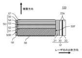
- FIG. 2 is a schematic cross-sectional view showing the semiconductor laser device 100 according to the first embodiment.
- FIG. 2 shows a cross-section of the semiconductor laser element 100 along a plane along the lamination direction of each layer of the semiconductor laminate 50 (described later) and the emission direction of the laser light.
- the semiconductor laser device 100 is a semiconductor light emitting device that emits a plurality of laser beams, a so-called semiconductor laser array.
- the semiconductor laser device 100 is a gallium nitride-based semiconductor laser device, and emits laser light having a wavelength in a band of about 390 nm to 530 nm.
- the semiconductor laser element 100 includes a semiconductor laminate 50, an emitting-side protective layer 1F, and a non-emitting-side protective layer 1R.
- the semiconductor laminate 50 is a laminate of a plurality of semiconductor layers.
- the semiconductor laminate 50 has a substrate 51 , a first semiconductor layer 52 , an active layer 53 , a second semiconductor layer 54 and a contact layer 55 .
- the substrate 51 is a plate-like member that serves as the base material of the semiconductor laminate 50 .
- the substrate 51 is a GaN single crystal substrate.
- the thickness of the substrate 51 is, for example, approximately 100 ⁇ m.
- the material forming the substrate 51 may be single crystal such as Al 2 O 3 (sapphire), SiC, GaAs, or InP. Also, the thickness of the substrate 51 may be, for example, 50 ⁇ m or more and 120 ⁇ m or less.
- the first semiconductor layer 52 is a semiconductor layer formed above the substrate 51 .
- the first semiconductor layer 52 is an n-type semiconductor layer and includes an n-type clad layer.
- the n-type clad layer is a layer made of n-Al 0.2 Ga 0.8 N.
- the thickness of the n-type clad layer is, for example, about 1 ⁇ m.
- the n-type cladding layer may be made of, for example, n-Al x Ga 1-x N (0 ⁇ x ⁇ 1). Also, the thickness of the n-type cladding layer may be, for example, 0.5 ⁇ m or more and 5 ⁇ m or less.
- an n-type Al x InyGa 1-x-yN (0 ⁇ x+y ⁇ 1) guide layer or an undoped Al x InyGa 1-x-yN (0 ⁇ x+y ⁇ 1) guide layer is formed on the n-type cladding layer. may be formed.
- the active layer 53 is a layer formed above the first semiconductor layer 52 .
- the active layer 53 functions as a light emitting layer.
- the active layer 53 has two well layers.
- the active layer 53 is a quantum well active layer in which well layers made of In 0.18 Ga 0.82 N and barrier layers made of GaN are alternately laminated.
- the thickness of the well layer is, for example, approximately 5 nm
- the thickness of the barrier layer is, for example, approximately 10 nm.
- the active layer 53 is composed of a well layer made of InxGa1 -xN (0 ⁇ x ⁇ 1) and AlxInyGa1 -x-yN (0 ⁇ x+y ⁇ 1) . Quantum well active layers in which barrier layers are alternately laminated may be used.
- the active layer 53 may have a guide layer at least one of above and below the quantum well active layer. Although the number of well layers is two in this embodiment, it may be one to four. In addition, the In composition of the well layer may be appropriately selected so that light with a desired wavelength is emitted within the wavelength range of 390 nm or more and 530 nm or less.
- the second semiconductor layer 54 is a semiconductor layer formed above the active layer 53 .
- the second semiconductor layer 54 is a p-type semiconductor layer and includes a p-type clad layer.
- the p-type cladding layer is a superlattice layer in which 100 layers of p-Al 0.2 Ga 0.8 N and 100 layers of GaN are alternately laminated.
- the thickness of the p-Al 0.2 Ga 0.8 N layer is, for example, approximately 3 nm, and the thickness of the GaN layer is, for example, approximately 3 nm.
- the p-type cladding layer may be a layer formed of Al x Ga 1-x N (0 ⁇ x ⁇ 1) instead of the superlattice layer described above.
- the thickness of this layer may be, for example, 0.3 ⁇ m or more and 1 ⁇ m or less.
- the p-type clad layer may be a bulk clad layer made of Al x Ga 1-x N (0 ⁇ x ⁇ 1).
- AlGaN is used as the material of the p-type clad layer.
- the reason is that AlGaN has a refractive index suitable for confining laser light in the active layer 53 .
- Materials other than AlGaN may be used as the material of the p-type cladding layer.
- ITO may be used as the material of the p-type clad layer.
- a material that transmits emitted laser light such as a transparent dielectric oxide such as In 2 O 3 , Ga 2 O 3 , SnO, or InGaO 3 may be used.
- the second semiconductor layer 54 includes a p-type Al x In y Ga 1-x-y N (0 ⁇ x+y ⁇ 1) guide layer and undoped Al x In y Ga 1-x under the p-type cladding layer.
- a plurality of -yN (0 ⁇ x+y ⁇ 1) guide layers may be provided.
- the contact layer 55 is a semiconductor layer formed above the second semiconductor layer 54 and is in ohmic contact with the second electrode 57 .
- the contact layer 55 is a p-type semiconductor layer made of p-GaN.
- the thickness of the contact layer 55 is, for example, approximately 10 nm.
- the material of the contact layer 55 is not limited to p-GaN. Also, the thickness of the contact layer 55 may be, for example, 5 nm or more and 200 nm or less.
- two or more ridges are formed in the second semiconductor layer 54 and contact layer 55 .
- a region of the active layer 53 corresponding to each ridge portion serves as a light emitting point, and laser light is emitted from a plurality of light emitting points.
- a first electrode 56 is arranged as an electrode on the lower main surface of the substrate 51 (that is, the main surface on which the first semiconductor layer 52 and the like are not arranged).
- the first electrode 56 is an n-side electrode and has a laminated structure in which a Ti layer, a Pt layer, and an Au layer are laminated in order from the substrate 51 side.
- the first electrode 56 may have another laminated structure, for example, a laminated structure in which a Ti layer and an Au layer are laminated.
- a second electrode 57 is arranged on the contact layer 55 as an electrode.
- the second electrode 57 has a p-side electrode that makes ohmic contact with the contact layer 55 and a pad electrode that is arranged on the p-side electrode.
- the p-side electrode has a laminated structure in which a Pd layer and a Pt layer are laminated in order from the contact layer 55 side. Also, the configuration of the p-side electrode is not limited to this.
- the p-side electrode may have a single layer structure or a multilayer structure including at least one of a Cr layer, Ti layer, Ni layer, Pd layer, Pt layer and Au layer, for example.
- the p-side electrode may be an ITO layer used as a transparent oxide electrode, an In 2 O 3 layer, a Ga 2 O 3 layer, an SnO layer, or an InGaO 3 layer.
- the pad electrode is a pad-shaped electrode arranged above the p-side electrode.
- the pad electrode has a laminated structure in which layers formed of a Ti layer and an Au layer are laminated in order from the p-side electrode side, and are arranged on the ridge and its periphery.
- the pad electrode may be composed of, for example, only an Au layer, or may have a laminated structure in which a Ti layer, a Pt layer and an Au layer are laminated, or a laminated structure in which a Ni layer and an Au layer are laminated. may be Also, the pad electrode may have a laminated structure in which two or more layers made of another metal are laminated.
- the semiconductor laminate 50 may further include an insulating layer such as an SiO 2 film covering the sidewalls of the ridge.
- Non-emission-side protective layer 1R is a layer arranged on the laser light non-emission-side facet 50R of the semiconductor laminate 50 (hereinafter referred to as "non-emission-side facet 50R").
- the non-emission-side protective layer 1R protects the non-emission-side facet 50R and increases the reflectance of the non-emission side of the semiconductor laminate 50 with respect to laser light to a certain value (eg, 90%) or higher.
- the “reflectance on the non-emission side” means the reflectance that is comprehensively evaluated by combining the non-emission-side end surface 50R and the non-emission-side protective layer 1R.
- the non-emission-side protective layer 1R has a multi-layer structure in which a plurality of pairs of SiO 2 layers and AlO 1-x N x (0 ⁇ x ⁇ 1) layers are laminated.
- the thicknesses of the SiO 2 layer and the AlO 1-x N x (0 ⁇ x ⁇ 1) layer are, for example, SiO 2 layer and AlO 1-x N x (0 ⁇ x ⁇ 1), where ⁇ a is the average wavelength of a plurality of laser beams. ⁇ 1)
- ⁇ a is the average wavelength of a plurality of laser beams.
- ⁇ 1 When the refractive index of each layer is n, it is approximately ⁇ a/(4n).
- the reflectance of the non-emission side with respect to the laser light becomes 90% or more.
- the semiconductor laser device 100 with high slope efficiency and low threshold current can be realized.
- the laminated structure of the non-emitting side protective layer 1R is not limited as long as a desired value of reflectance on the non-emitting side can be obtained.
- the non-emission-side protective layer 1R includes a set of SiO 2 layer and ZrO 2 layer, a set of SiO 2 layer and Ta 2 O 5 layer, a set of SiO 2 layer and AlN layer, a set of SiO 2 layer and TiO 2 layer. , a set of SiO 2 layers and HfO 2 layers, a set of SiO 2 layers and Nb 2 O 5 layers, or a set of SiO 2 layers and Al 2 O 3 layers, etc. good.
- the Al 2 O 3 layer may be used as the low refractive index layer.
- the non-emission-side protective layer 1R may have a single-layer structure or a multi-layer structure including at least one of an oxynitride layer and a nitride layer.
- the emission-side protective layer 1F is a layer arranged on the laser light emission-side facet 50F of the semiconductor laminate 50 (hereinafter referred to as the "emission-side facet 50F").
- the emission-side protective layer 1F protects the emission-side facet 50F and reduces the reflectance of the semiconductor laminate 50 on the emission side of the laser beam.
- the “output-side reflectance” means the reflectance that is comprehensively evaluated by combining the output-side end face 50F and the output-side protective layer 1F.
- the exit-side protective layer 1F includes a barrier layer 21 and a control layer 22.
- the reflectance on the output side may be simply called "reflectance”.
- the barrier layer 21 is arranged in contact with the emission-side end surface 50F.
- the barrier layer 21 has a function of suppressing deterioration of the output-side facet 50 ⁇ /b>F of the semiconductor stacked body 50 .
- the barrier layer 21 is a dielectric layer, specifically an oxynitride layer or a nitride layer.
- the barrier layer 21 is a single layer made of AlO 1-x N x (0 ⁇ x ⁇ 1), for example. Moreover, the thickness of the barrier layer 21 is, for example, about 20 nm.
- the barrier layer 21 may be, for example, an oxynitride layer such as a SiO 1-x N x (0 ⁇ x ⁇ 1) layer, or a nitride layer such as an AlN layer or a SiN layer. may
- the control layer 22 is arranged in contact with the emission-side surface of the barrier layer 21 .
- the control layer 22 has a function of adjusting the reflectance of the output side of the semiconductor laminate 50 . More specifically, the control layer 22 suppresses the reflectance on the emission side to a predetermined value (for example, 1%) or less for each oscillation wavelength of the laser light.
- the control layer 22 has a main control layer 22a that contributes to adjusting the reflectance, and a strain relaxation layer 30 that relaxes the strain of the control layer 22 as a whole.
- the main control layer 22a and the strain relaxation layer 30 are made of different materials.
- the main control layer 22a is a dielectric layer, specifically an oxynitride layer, a nitride layer, or an oxide layer.
- the main control layer 22a is a layer made of Al2O3 , for example.
- the total thickness of the main control layer 22a on both sides of the strain relaxation layer 30 is, for example, about 55 nm.
- the main control layer 22a is an oxynitride layer such as an AlO 1-x N x (0 ⁇ x ⁇ 1) layer or a SiO 1-x N x (0 ⁇ x ⁇ 1) layer, an AlN layer, or an SiN layer. It may be a nitride layer, such as a layer, or an oxide layer, such as TiO 2 layer, Nb 2 O 5 layer, ZrO 2 layer, Ta 2 O 5 layer, or HfO 2 layer. Since the main control layer 22a has such a structure, the reflectance on the output side can be suppressed to 1% or less for each wavelength of laser light. As a result, stable external resonance characteristics can be realized in a laser device including the semiconductor laser element 100 .
- the strain relaxation layer 30 is arranged so as to be inserted at an intermediate position in the control layer 22 in the traveling direction of the laser light. That is, the strain relaxation layer 30 is sandwiched between two main control layers 22a.
- the two main control layers 22a may be made of the same material, or may be made of different materials.
- the strain relaxation layer 30 has a function of suppressing strain due to thermal expansion of the entire emission-side protective layer 1F including the control layer 22. It should be noted that the thermal expansion of the control layer 22 is caused by the heat generated by the emitted laser light.
- the strain relaxation layer 30 is a dielectric layer, and has a smaller thermal expansion coefficient than at least the main control layer 22a.
- the strain relaxation layer 30 is made of a material having the smallest coefficient of thermal expansion among the layers included in the output-side protective layer 1F.
- a material with low light absorption in the wavelength range near the 450 nm band is selected in order to suppress light absorption of laser light.
- the strain relaxation layer 30 is made of SiO2 .
- SiO 2 is a substance with a relatively small thermal expansion coefficient and little light absorption in the vicinity of the 450 nm band. Also, since SiO 2 is an oxide layer, it is less susceptible to the effects of surrounding layers and the outside air.
- ⁇ Action of strain relaxation layer> When a laser beam is emitted from the semiconductor laser element 100, the vicinity of the emission-side facet 50F becomes a high temperature state, and the emission-side protective layer 1F thermally expands. At this time, tensile stress is generated at the interface between the semiconductor laminate 50 and the output-side protective layer 1F. In particular, when a part of the exit-side protective layer 1F includes a layer formed of a material having a large coefficient of thermal expansion, the tensile stress increases.
- the entire output-side protective layer 1F including the control layer 22 can be restrained from being strained due to thermal expansion. More specifically, the thermal expansion of the output-side protective layer 1F can be suppressed, and the tensile stress generated at the interface between the output-side protective layer 1F and the output-side end surface 50F can be reduced.
- SiO 2 forming the strain relaxation layer 30 has a smaller thermal expansion coefficient than Al 2 O 3 or the like forming the main control layer 22a. Therefore, by arranging the strain relaxation layer 30 between the two main control layers 22a (Al 2 O 3 layers), it is possible to effectively suppress strain due to thermal expansion of the output-side protective layer 1F.
- the material for the strain relaxation layer 30 should have a smaller thermal expansion coefficient than the material for the main control layer 22a. It is more desirable if the material of the strain relaxation layer 30 is a material with the smallest coefficient of thermal expansion among the layers included in the output-side protective layer 1F.
- the light absorption is small with respect to the oscillation wavelength of each laser light (for example, the extinction coefficient is 2.0 ⁇ 10 ⁇ 3 or less)
- materials other than SiO 2 may be used.
- the strain relaxation layer 30 does not necessarily have to be a SiO 2 layer.
- the strain relaxation layer 30 is, for example, another dielectric layer with a small thermal expansion coefficient, such as an AlN layer, a nitride layer such as an SiN layer, an AlO 1-x N x (0 ⁇ x ⁇ 1) layer, or , SiO 1-x N x (0 ⁇ x ⁇ 1) layers, or oxynitride layers, or oxide layers such as Al 2 O 3 layers, Ta 2 O 5 layers, or HfO 2 layers. good.
- the total thickness of the main control layer 22a is, for example, about 55 nm.
- the thickness of the strain relaxation layer 30 may be 2 nm or less, and is 1 nm in this embodiment.
- the semiconductor laser device 100 does not have the strain relaxation layer 30 and does not have the emission side protective layer 30 except for the fact that it does not have the strain relaxation layer 30 .
- the wavelength characteristics with respect to the laser light are equivalent.
- the output-side protective layer without the strain relaxation layer 30 is disposed on the output-side facet 50F, the output-side reflectance is 1.0% or less for each oscillation wavelength of the laser light.
- the main control layer 22a so as to suppress it, even if the strain relaxation layer 30 is added to the output side protective layer 1F, the output side reflectance can be maintained at 1.0% or less.
- the output-side protective layer without the strain relaxation layer 30 when the output-side protective layer without the strain relaxation layer 30 is disposed on the output-side facet 50F, the output-side reflectance is 1.0 for each oscillation wavelength of the laser light. % or less, the main control layer 22a is configured. Therefore, although the semiconductor laser device 100 according to the present embodiment has the strain relaxation layer 30, the reflectance on the emission side can be maintained at 1.0% or less. Therefore, a stable external resonance characteristic can be realized in a laser device including the semiconductor laser element 100.
- the strain relief layer 30 may exist at any position on the control layer 22 . That is, the main control layer 22a is arranged so that the reflectance on the output side is 1% or less with respect to the oscillation wavelength of each laser beam when the output-side protective layer without the strain relaxation layer 30 is arranged. is configured, regardless of the position of the strain relaxation layer 30 in the control layer 22, the reflectance on the output side is suppressed to 1% or less with respect to the oscillation wavelength of each laser beam.
- a semiconductor wafer which is the base of the semiconductor laminate 50, is formed.
- a substrate 51 is prepared.
- a first semiconductor layer 52 as an n-type clad layer, an active layer 53, a second semiconductor layer 54 as a p-type clad layer, and a contact layer 55 are laminated in this order on the substrate 51 .
- Each layer can be formed by, for example, a metal organic chemical vapor deposition (MOCVD) method.
- MOCVD metal organic chemical vapor deposition
- a ridge portion is formed in the second semiconductor layer 54 and the contact layer 55 .
- the ridge portion can be formed by, for example, high-frequency inductively coupled plasma (ICP) type reactive ion etching.
- ICP inductively coupled plasma
- a semiconductor wafer is formed through the above process.
- an insulating layer such as a SiO 2 layer is formed on the entire surface by, for example, plasma CVD. Then, at least part of the upper surface of the ridge portion of the insulating layer is removed by wet etching or the like, and an insulating layer is formed on the sidewalls of the ridge portion.
- a second electrode 57 and a first electrode 56 are formed on the region where the insulating layer on the ridge is removed and on the lower surface of the substrate 51 by vacuum deposition or the like.
- the semiconductor laminate 50 having the emitting side facet 50F and the non-emitting side facet 50R is formed as a laser bar.
- an output-side protective layer 1F and a non-output-side protective layer 1R are formed on the output-side end surface 50F and the non-output-side end surface 50R of the semiconductor laminate 50, respectively.
- a solid source ECR (Electron Cyclotron Resonance) sputtering plasma deposition apparatus is used to form a dielectric layer. By using this apparatus, it is possible to suppress damage to the exit-side facet 50F and the already formed layers when forming each layer of the exit-side facet 50F.
- the emission-side facet 50F and the non-emission-side facet 50R may be formed using a vapor deposition device or the like, an ablation deposition device using PLD (PULSE Laser Deposition) or ALD (Atomic Layer Deposition), or , an epitaxial growth apparatus using MOCVD, or the like.
- a vapor deposition device or the like an ablation deposition device using PLD (PULSE Laser Deposition) or ALD (Atomic Layer Deposition), or , an epitaxial growth apparatus using MOCVD, or the like.
- the semiconductor laser device 100 according to this embodiment is manufactured through the above processes.
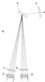
- FIG. 3 is a schematic diagram showing a semiconductor laser device 90 including the semiconductor laser element according to the first embodiment.
- the semiconductor laser device 90 is an external resonator type semiconductor laser device that combines wavelengths.
- a semiconductor laser device 90 includes semiconductor laser elements 101 and 102 , optical lenses 91 and 92 , a diffraction grating 95 and a partially reflecting mirror 97 .
- the semiconductor laser elements 101 and 102 are elements having the same structure and the same function as the semiconductor laser element 100 according to the first embodiment.
- the semiconductor laser elements 101 and 102 are laser array elements having a plurality of light emitting points. That is, the semiconductor laser elements 101 and 102 are used as small laser light sources that emit a plurality of laser beams. Therefore, the semiconductor laser device 90 can be, for example, a small semiconductor laser device on which the semiconductor laser elements 101 and 102 are mounted.
- Each of the semiconductor laser elements 101 and 102 has N light emitting points E11 to E1N (N is an integer equal to or greater than 2) and N light emitting points E21 to E2N.
- a plurality of laser beams are emitted from the light emitting points E11 to E1N.
- a plurality of laser beams are emitted from the light emitting points E21 to E2N.
- the wavelength of the laser light emitted from each light emitting point is determined according to the wavelength selection action by the external resonator including the diffraction grating 95 . Therefore, a plurality of laser beams having different wavelengths ⁇ 11 to ⁇ 1N are emitted from the light emitting points E11 to E1N as external resonance laser beams.
- a plurality of laser beams of ⁇ 2N are emitted as external resonance laser beams.
- the semiconductor laser elements 101 and 102 are arranged so that a plurality of laser beams propagate within the same plane.
- the optical lenses 91 and 92 are optical elements that condense a plurality of laser beams emitted from the semiconductor laser elements 101 and 102 onto the diffraction grating 95 .
- the optical lenses 91 and 92 may have a function of collimating the laser light.
- the semiconductor laser device 90 may include a collimating lens for collimating each laser beam.
- the diffraction grating 95 is a wavelength dispersive element that multiplexes a plurality of laser beams having different wavelengths, and is specifically a transmissive diffraction grating.
- a plurality of laser beams with different propagation directions can be transmitted on substantially the same optical axis. Can be synthesized.
- the diffraction grating 95 may be an element other than a transmissive diffraction grating, such as a prism or a reflective diffraction grating.
- the partially reflecting mirror 97 forms an external resonator with the non-emitting end faces of the semiconductor laser elements 101 and 102 .
- the partially reflecting mirror 97 functions as an output coupler that transmits (that is, emits) a portion of the laser light.
- the reflectance and transmittance of the partially reflecting mirror 97 are appropriately set according to the gains of the semiconductor laser elements 101 and 102 and the like.
- the semiconductor laser elements 101 and 102 each emit N laser beams when current is supplied.
- the N laser beams emitted from the semiconductor laser element 101 are condensed at a condensing point on the diffraction grating 95 by the optical lens 91 . Also, the N laser beams emitted from the semiconductor laser element 102 are condensed at a condensing point on the diffraction grating 95 by the optical lens 92 . Note that the laser light from the semiconductor laser element 101 and the laser light from the semiconductor laser element 102 are condensed at the same condensing point.
- the 2N laser beams are diffracted by the diffraction grating 95 and propagate along substantially the same optical axis toward the partially reflecting mirror 97 .
- a part of the laser light incident on the partial reflection mirror 97 is reflected by the partial reflection mirror 97, returns to the semiconductor laser element 101 or 102 via the diffraction grating 95 and the optical lens 91 or 92, and is reflected by each element. It is reflected by the output side end surface 50R. In this manner, an external resonator is formed between the non-emitting end face 50R of the semiconductor laser elements 101 and 102 and the partially reflecting mirror 97.
- the semiconductor laser elements 101 and 102 are arranged together with the optical lenses 91 and 92, the diffraction grating 95 and the partially reflecting mirror 97 to form an external resonator.
- the other portion of the laser light directed from the diffraction grating 95 toward the partially reflecting mirror 97 is transmitted through the partially reflecting mirror 97 and becomes the output light of the semiconductor laser device 90 .
- the output light is output as high-output laser light to the outside of the semiconductor laser device 90 via, for example, an optical fiber arranged on the optical axis of the output light.
- the wavelength synthesizing method used in the semiconductor laser device 90 of FIG. 3 and a spatial synthesizing method for spatially synthesizing laser beams.
- the wavelength combining method of condensing light of different wavelengths on the same optical axis is more advantageous than the spatial combining method.
- the optical path lengths from the emission side facet 50F to the diffraction grating 95 and the incident angles with respect to the diffraction grating 95 of the laser beams with wavelengths ⁇ 11 to ⁇ 1N emitted from the semiconductor laser element 101 are different from each other.
- the optical path lengths from the emission side facet 50F to the diffraction grating 95 and the incident angles with respect to the diffraction grating 95 of the laser beams with wavelengths ⁇ 21 to ⁇ 2N emitted from the semiconductor laser element 102 are different from each other. Therefore, the laser beams of different wavelengths ⁇ 11 to ⁇ 1N and ⁇ 21 to ⁇ 2N are diffracted by the diffraction grating 95, thereby changing the wavelengths of the laser beams.
- the semiconductor laser device 90 includes two semiconductor laser elements 101 and 102 in this embodiment, the semiconductor laser device 90 may include three or more semiconductor laser elements. As the number of semiconductor laser elements included in the semiconductor laser device 90 increases, the optical output value of the semiconductor laser device 90 can be increased.
- a plurality of semiconductor laser devices 90 that combine wavelengths may be used, and the output light from the semiconductor laser devices 90 may be combined by a spatial combining method to further increase the optical output.
- the semiconductor laser device 100 includes the semiconductor laminate 50 that emits laser light, the emission-side protective layer 1F disposed on the emission-side facet 50F of the semiconductor laminate 50, and the semiconductor laminate. and a non-emission-side protective layer 1R disposed on the end face (non-emission-side end face 50R) opposite to the emission-side end face 50F of the body 50 and reflecting the laser light.
- the output-side protective layer 1F has a control layer 22 that suppresses the reflectance on the output side with respect to the wavelength of the laser light to a predetermined value or less, and the control layer 22 suppresses distortion due to thermal expansion of the control layer 22. It has a strain relief layer 30 .
- the reflectance on the output side of the semiconductor laminate 50 can be maintained at a predetermined value or less.
- the thermal expansion of the output-side protective layer 1F can be suppressed, and the tensile stress generated at the interface between the output-side end surface 50F of the semiconductor laminate 50 and the output-side protective layer 1F can be reduced, deterioration of the output-side end surface 50F and deterioration of the output-side protective layer 1F can be prevented. Peeling of the protective layer 1F can be suppressed.
- the semiconductor laminate 50 has a plurality of light emitting points located on the emitting side facet 50F and emitting a plurality of laser beams. Moreover, the reflectance on the output side is less than or equal to a predetermined value with respect to the wavelength of the laser light.
- the semiconductor laser device 100 can emit a plurality of laser beams and can output high-quality laser beams. Further, by mounting the above-described semiconductor laser device 100 in an external resonator type semiconductor laser device 90 that performs wavelength synthesis, a semiconductor laser device that outputs high-quality laser light can be realized.
- the semiconductor laser device 100 when used in an external cavity type semiconductor laser device 90 that performs wavelength synthesis, an external cavity is formed between the partially reflecting mirror 97 and the non-emitting facet of the semiconductor laser device. That is, a plurality of laser beams having different wavelengths are transmitted through the emission-side protective layer 1F.
- the reflectance on the emission side with respect to the wavelength of each laser beam can be reduced. can be suppressed to a predetermined value or less. Therefore, the configuration and manufacturing process of the semiconductor laser device 90 can be simplified. That is, manufacturing errors of the semiconductor laser device can be reduced, the manufacturing process can be stabilized, and cost reduction can be realized.
- the reflectance on the emission side with respect to the wavelength of the laser light emitted from the semiconductor laser element 100 is suppressed to 1.0% or less.
- the strain relaxation layer 30 is arranged at an intermediate position in the control layer 22 in the traveling direction of the laser light.
- the exit-side protective layer 1F further has a barrier layer 21 arranged between the exit-side end face 50F and the control layer 22.
- the semiconductor laser element 100 is a gallium nitride-based semiconductor laser element
- diffusion of oxygen from the outside of the output-side protective layer 1F to the semiconductor laminate 50 easily deteriorates the output-side protective layer 1F and the output-side facet 50F.
- the barrier layer 21 on the output-side protective layer 1F
- diffusion of oxygen from the outside of the output-side protective layer 1F to the semiconductor stacked body 50 can be reduced. Therefore, it is possible to suppress the deterioration of the output-side protective layer 1F and the exit-side end surface 50F. Therefore, the reliability of the output of the semiconductor laser device 100 can be improved, and the operation period can be lengthened.
- the emission-side protective layer 1F tends to be thick.
- the thicker the output-side protective layer 1F the greater the tensile stress generated at the interface between the output-side protective layer 1F and the output-side end surface 50F when the output-side protective layer 1F thermally expands. Therefore, the emission-side end surface 50F is likely to deteriorate.
- the exit-side protective layer 1F of this embodiment has a barrier layer 21 and is relatively thick as a whole. However, the exit-side protective layer 1F has the control layer 22 including the strain relaxation layer 30. FIG. Therefore, in a device that emits high-energy laser light, such as a gallium nitride-based semiconductor laser device, it is possible to output high-energy laser light and improve the quality of the laser light while keeping the reflectance on the emission side low. can.
- the protection performance of the exit-side facet 50F can be enhanced.
- the thickness of the strain relaxation layer 30 is 2 nm or less.
- strain relaxation layer 30 Since the strain relaxation layer 30 is thin, even if the control layer 22 has the strain relaxation layer 30, compared with the emission side protective layer without the strain relaxation layer 30, the emission side of the output side for a plurality of wavelengths of laser light is reduced. Reflectance values and wavelength characteristics are unchanged.
- the strain relaxation layer 30 has the smallest coefficient of thermal expansion among the layers included in the output-side protective layer 1F.
- the strain relaxation layer 30 is made of SiO 2 .
- SiO 2 has a particularly small coefficient of thermal expansion (approximately 0.5), so deterioration of the emission-side facet 50F can be further suppressed.
- SiO 2 has a low light absorption in the wavelength band of the laser light emitted from the gallium nitride based semiconductor laser device. Therefore, absorption of laser light by the strain relaxation layer 30 can be suppressed.
- FIG. 4 is a schematic cross-sectional view showing a semiconductor laser device 200 according to the second embodiment.
- FIG. 4 shows a cross section of the semiconductor laser element 200 along a plane along the lamination direction of each layer of the semiconductor layered body 50 provided in the semiconductor laser element 200 and the emission direction of the laser light.
- the semiconductor laser element 200 is a semiconductor light emitting element that emits a plurality of laser beams.
- the semiconductor laser device 200 is a gallium nitride based semiconductor laser device.
- the semiconductor laser element 200 includes a semiconductor laminate 50, an emitting side protective layer 2F, and a non-emitting side protective layer 1R.
- the semiconductor laser device 200 differs from the semiconductor laser device 100 according to the first embodiment only in the structure and function of the emission-side protective layer 2F, and is otherwise the same in structure and function.
- the exit-side protective layer 2 ⁇ /b>F has a barrier layer 21 and a control layer 22 .
- the barrier layer 21 of the first embodiment has a single-layer structure
- the barrier layer 21 of this embodiment has a two-layer structure composed of the first layer 31 and the second layer 32 .
- the first layer 31 is in contact with the emission-side end surface 50F of the semiconductor laminate 50.
- the first layer 31 is a dielectric layer, specifically an oxynitride layer or a nitride layer.
- the first layer 31 is the same material as the barrier layer 21 of the first embodiment.
- the first layer 31 is a layer made of AlO 1-x N x (0 ⁇ x ⁇ 1), for example.
- the thickness of the first layer 31 is, for example, about 20 nm.
- the first layer 31 may be an oxynitride layer such as a SiO 1-x N x (0 ⁇ x ⁇ 1) layer, or a nitride layer such as an AlN layer or a SiN layer.
- the second layer 32 is a layer arranged in contact with the output side surface of the first layer 31 .
- the second layer 32 has a function of enhancing the protection performance of the emission-side end surface 50F.
- the second layer 32 is a dielectric layer, specifically an oxynitride layer, a nitride layer, or an oxide layer.
- the second layer 32 is a layer made of Al 2 O 3 , for example.
- the thickness of the second layer 32 is, for example, about 10 nm.
- the second layer 32 is a SiO 1-x N x (0 ⁇ x ⁇ 1) layer, an oxynitride layer such as an AlO 1-x N x (0 ⁇ x ⁇ 1) layer, a SiN layer, or , a nitride layer such as an AlN layer, or an oxide layer such as a SiO2 layer.
- the control layer 22 is farther from the emission-side end surface 50F than the barrier layer 21 and is arranged in contact with the emission side surface of the barrier layer 21 .
- the control layer 22 has an inner layer 33 , an intermediate layer 34 and an outer layer 35 . These layers are all dielectric layers, and are arranged in order of the inner layer 33 , the intermediate layer 34 and the outer layer 35 from the side closer to the barrier layer 21 .
- control layer 22 Since the control layer 22 has three types of layers, the inner layer 33, the intermediate layer 34, and the outer layer 35, the reflectance on the output side is 1% or less for a wider range of wavelengths than in the first embodiment. can be suppressed to
- the inner layer 33 is a layer made of Al2O3 , for example.
- the thickness of the inner layer 33 is, for example, about 100 nm.
- the outer layer 35 is, for example, a layer made of SiO2 .
- the thickness of the outer layer 35 is, for example, about 100 nm.
- the intermediate layer 34 has a main intermediate layer 34 a that contributes to adjusting the reflectance, and a strain relaxation layer 30 that relaxes the strain of the control layer 22 as a whole.
- the materials of the main intermediate layer 34a and the strain relaxation layer 30 are different.
- the main intermediate layer 34a is, for example, a layer made of ZrO2 .
- the main intermediate layer 34a may be a layer formed of a material having a higher refractive index with respect to laser light than either of the inner layer 33 and the outer layer 35 .
- the main intermediate layer 34a is, for example, an AlO 1-x N x (0 ⁇ x ⁇ 1) layer, an oxynitride layer such as a SiO 1-x N x (0 ⁇ x ⁇ 1) layer, a SiN layer, or , a nitride layer such as an AlN layer, an oxide layer such as a TiO 2 layer, a Nb 2 O 5 layer, a Ta 2 O 5 layer, or an HfO 2 layer.
- the inner layer 33 may be a layer other than the Al 2 O 3 layer. If the inner layer 33 is a layer other than an Al2O3 layer, the main intermediate layer 34a may be an Al2O3 layer.
- the inner layer 33 and the outer layer 35 may be layers formed of a material having a lower refractive index for laser light than the main intermediate layer 34a.
- the inner layer 33 is, for example, an AlO 1-x N x (0 ⁇ x ⁇ 1) layer, an oxynitride layer such as a SiO 1-x N x (0 ⁇ x ⁇ 1) layer, or an SiO 2 layer. It may be an oxide layer such as
- the outer layer 35 is, for example, an AlO 1-x N x (0 ⁇ x ⁇ 1) layer, an oxynitride layer such as a SiO 1-x N x (0 ⁇ x ⁇ 1) layer, or an Al It may also be an oxide layer such as a 2 O 3 layer.
- the strain relaxation layer 30 is arranged so as to be inserted in an intermediate position of the intermediate layer 34 in the traveling direction of the laser light. That is, the strain relaxation layer 30 is sandwiched between two main intermediate layers 34a.
- the two main intermediate layers 34a may be made of the same material, or may be made of different materials.
- the strain relaxation layer 30 is made of SiO 2 and has a thickness of about 2 nm, as in the first embodiment. On the other hand, the total thickness of the main intermediate layers 34a on both sides of the strain relaxation layer 30 is, for example, about 50 nm.
- the strain relaxation layer 30 may be made of a material having a smaller thermal expansion coefficient than at least the main intermediate layer 34a. More desirably, the strain relaxation layer 30 is made of a material having the smallest coefficient of thermal expansion among the layers included in the output-side protective layer 2F. Further, the strain relaxation layer 30 may be an AlO 1-x N x (0 ⁇ x ⁇ 1) layer or a SiO 1-x N layer depending on the materials of the layers other than the strain relaxation layer 30 in the output-side protective layer 2F.
- an oxynitride layer such as an x (0 ⁇ x ⁇ 1) layer, a nitride layer such as an AlN layer or a SiN layer, or an Al 2 O 3 layer, a Ta 2 O 5 layer or a HfO 2 layer It may be an oxide layer.
- control layer 22 has the strain relaxation layer 30, so that the same effect as in the first embodiment can be obtained.
- control layer 22 since the control layer 22 has the strain relaxation layer 30 made of a material with a small thermal expansion coefficient, the tensile stress generated at the interface between the output-side protective layer 2F and the output-side end surface 50F can be reduced. Therefore, the reflectance of the semiconductor laser element 200 on the emission side can be reduced, and the laser quality can be improved.
- the strain relaxation layer 30 is arranged at an intermediate position in the intermediate layer 34 in the traveling direction of the laser light. Therefore, it is possible to further suppress distortion due to thermal expansion of the output-side protective layer 2F as a whole, and to further suppress deterioration of the output-side protective layer 2F.
- the thickness of the strain relaxation layer 30 should be 2 nm or less.
- the semiconductor laser device 200 does not have the strain relaxation layer 30, and the output side is protected in the points other than not having the strain relaxation layer 30.
- the wavelength characteristics with respect to laser light are equivalent.
- the control layer 22 of this embodiment has an inner layer 33, a main intermediate layer 34a, and an outer layer 35, and an output-side protective layer without the strain relaxation layer 30 is disposed on the output-side end surface 50F.
- the inner layer 33, the main intermediate layer 34a, and the outer layer 35 are configured so that the reflectance on the output side is suppressed to 1.0% or less for each oscillation wavelength of the laser light. . Therefore, the reflectance on the output side of the laser light can be suppressed to 1.0% or less.
- the reflectance on the output side can be suppressed to 1.0% or less for a wider range of wavelengths.
- the semiconductor laser device 200 of the second embodiment has the output side facet 50F, so that the reflectance on the output side is 1% for wavelengths included in a wavelength range with a wavelength width of 50 nm or more. can be reduced to the following.
- the reflectance on the output side can be appropriately changed.
- the strain relaxation layer 30 has substantially the same reflectance and wavelength characteristics on the exit side regardless of the position of the strain relaxation layer 30 on the control layer 22 . That is, the strain relief layer 30 may be placed anywhere in the control layer 22 , for example, the inner layer 33 or the outer layer 35 may have the strain relief layer 30 .
- the barrier layer 21 of the second embodiment has a two-layer structure, it may have a layer structure composed of three or more layers.
- at least the layer in contact with the emission-side facet 50F should be a layer corresponding to the first layer 31, that is, an oxynitride layer or a nitride layer.
- the two or more layers other than the layer in contact with the output-side facet 50F are necessarily AlO 1-x N x (0 ⁇ x ⁇ 1) layers or SiO 1-x N x (0 ⁇ x ⁇ 1) layers. It may not be an oxynitride layer, or a nitride layer such as an AlN layer or a SiN layer, but may be an oxide layer such as an Al2O3 layer or an SiO2 layer.
- the first layer 31 may have a multi-layer structure composed of at least one layer of an oxynitride layer and a nitride layer.
- the semiconductor laser device 200 is a gallium nitride based semiconductor laser device, and the barrier layer 21 includes the first layer 31 which is an oxynitride layer or a nitride layer. .
- the first layer 31 on the output-side facet 50F By arranging the first layer 31 on the output-side facet 50F, diffusion of oxygen from the outside of the output-side protective layer 2F to the semiconductor laminate 50 can be reduced. Therefore, the deterioration of the emission-side protective layer 2F can be suppressed, the reliability of the output of the semiconductor laser device 100 can be improved, and the operation period can be lengthened.
- the layer (first layer 31) in contact with the emission-side facet 50F is an oxynitride layer or a nitride layer having the same crystallinity as the semiconductor stacked body 50. Therefore, it is possible to enhance the protective performance of the emission-side end surface 50F.
- the barrier layer 21 includes, in addition to the first layer 31, a second layer 32 which is an oxynitride layer, a nitride layer, or an oxide layer.
- the diffusion of oxygen from the outside of the emission-side protective layer 2F to the semiconductor laminate 50 can be further reduced.
- deterioration of the emission-side facet 50F can be further suppressed, so that the quality of the laser light from the semiconductor laser device 100 can be further improved, and the operating period can be extended.
- the control layer 22 has an inner layer 33 , an intermediate layer 34 and an outer layer 35 , the inner layer 33 , the intermediate layer 34 and the outer layer 35 having the inner layer 33 , the intermediate layer 34 and the outer layer 35 with respect to the barrier layer 21 .
- 34 and the outer layer 35 are arranged in this order.
- the intermediate layer 34 has the strain relief layer 30 , and the main intermediate layer 34 a of the intermediate layer 34 is made of a material different from that of the inner layer 33 and the outer layer 35 .
- the refractive index of the main intermediate layer 34a for laser light is greater than that of both the inner layer 33 and the outer layer 35 for laser light.
- the reflectance on the output side can be suppressed to 1% or less for a wider range of wavelengths than in the first embodiment.
- the inner layer 33 and the outer layer 35 are AlO 1-x N x (0 ⁇ x ⁇ 1), SiO 1-x N x (0 ⁇ x ⁇ 1), SiO 2 and Al 2 O 3 respectively. is formed by Thus, inner layer 33 and outer layer 35 with relatively low refractive indices are realized.
- the main intermediate layer 34a is made of AlO 1-x N x (0 ⁇ x ⁇ 1), SiO 1-x N x (0 ⁇ x ⁇ 1), AlN, SiN, Al 2 O 3 , ZrO 2 , TiO 2 , Nb 2 O 5 , Ta 2 O 5 or HfO 2 . Therefore, the main intermediate layer 34a having a relatively high refractive index is realized.
- the output-side protective layers 1F and 2F have at least one or more of an oxynitride layer, a nitride layer, or an oxide layer in addition to the strain relaxation layer 30. Even with such a structure, the reflectance on the output side can be suppressed to a predetermined value or less, and the laser quality can be improved.
- the non-emission side protective layer 1R may have any layer structure as long as the reflectance on the non-emission side can be secured at a certain value or higher. As long as the non-emission-side protective layer 1R has at least one layer of an oxynitride layer, a nitride layer, or an oxide layer, any layer structure may be used. And the effects of the second embodiment are not reduced.
- the semiconductor laser device 100 has a plurality of light emitting points, but even if it has a single light emitting point, the same effect can be obtained. That is, it is possible to suppress the reflectance on the output side with respect to the wavelength of the laser light emitted from the semiconductor laser device 100 to a predetermined value or less, thereby realizing improvements in laser quality and output.
- the semiconductor laser element does not have to be a gallium nitride semiconductor laser element.
- the semiconductor laser device may be an AlGaInP semiconductor laser device, a gallium arsenide semiconductor laser device, or an InP semiconductor laser device.
- the semiconductor laser element is an AlGaInP-based semiconductor laser element
- the wavelength of the emitted laser light is in the red wavelength band (band of 600 nm or more and 700 nm or less).
- the semiconductor laser device is a gallium arsenide-based semiconductor laser device
- the wavelength of the emitted laser light is in the infrared wavelength band (750 nm or more and 1100 nm or less).
- the semiconductor laser element is an InP-based semiconductor laser element, the wavelength of the emitted laser light is in the 1 ⁇ m band.
- the semiconductor laser device 100 does not necessarily have to have the barrier layer 21 .
- the semiconductor laser device is an AlGaInP semiconductor laser device, a gallium arsenide semiconductor laser device, or an InP semiconductor laser device
- the diffusion of oxygen from the outside of the emission-side protective layers 1F and 2F to the semiconductor laminate 50 causes Deterioration of the outgoing end face 50F is less likely to occur.
- first embodiment Both the semiconductor laser device having the strain relaxation layer 30 (hereinafter referred to as “first embodiment”) and the semiconductor laser device having no strain relaxation layer 30 (hereinafter referred to as “comparative example”) were tested.
- the catastrophic optical damage (COD) level of the element was examined.
- the following conditions (1) and (2) are common to the first embodiment and the comparative example.
- (1) When the wavelength of the laser light emitted from the semiconductor laser element is ⁇ , the total thickness of the protective layer on the output side is approximately ⁇ /2.
- the thickness of the control layer 22 is about 3 ⁇ /8 Specifically, a reliability test was performed on the semiconductor laser devices of the first example and the comparative example, and the COD level was evaluated based on the change in optical output value before and after the reliability test. As a reliability test, the inventor continuously output laser light from the semiconductor laser devices of Examples and Comparative Examples for a long time (here, 1000 hours). The measurement results of the light output values of both devices are shown in Table 2 below.
- the light output value of the semiconductor laser device of the comparative example decreased significantly after the reliability test. That is, the COD level was significantly lowered.
- the amount of decrease in the optical output value after the reliability test was smaller than that before the reliability test. That is, it can be said that the decrease in the COD level was suppressed.
- the semiconductor laser device 100 according to the first embodiment has a strain relief layer in which the control layer 22 is made of a material having a smaller thermal expansion coefficient than the material of the main control layer 22a. has 30. Therefore, similarly to the semiconductor laser device of the first embodiment, it can be said that the tensile stress generated at the interface between the emission-side protective layer 1F and the emission-side facet 50F can be reduced, and deterioration of the emission-side facet 50F can be suppressed. Therefore, it can be said that the reflectance on the emission side of the semiconductor laser device 100 can be reduced and the laser quality can be improved.
- the semiconductor laser device 200 according to the second embodiment has the strain relief layer 30 in which the intermediate layer 34 of the control layer 22 is made of a material having a smaller thermal expansion coefficient than the material of the main intermediate layer 34a. Therefore, it can be said that an effect similar to that of the first embodiment can be obtained. Therefore, it can be said that the reflectance on the emission side of the semiconductor laser device 200 can be reduced and the laser quality can be improved.
- This appropriate value is the thickness of the strain relaxation layer 30 required to obtain the same reflectance as that of the semiconductor laser device having the emission side protective layer that does not include the strain relaxation layer 30. That is.
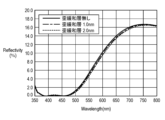
- FIG. 5 is a graph showing the reflectance on the emission side of the semiconductor laser device according to the second example.
- the solid line in FIG. 5 indicates the wavelength characteristics of the reflectance of a semiconductor laser device without a strain relaxation layer
- the one-dot chain line indicates the wavelength of the reflectance of a semiconductor laser device having a strain relaxation layer 30 with a thickness of 1 nm.
- the dashed line indicates the wavelength characteristics of the reflectance of the semiconductor laser device having the strain relaxation layer 30 with a thickness of 2 nm.
- These semiconductor laser devices according to the second example have control layers according to the second embodiment, that is, control layers composed of an inner layer, an intermediate layer, and an outer layer. Also, the intermediate layer of the semiconductor laser device having the strain relaxation layer 30 has a SiO 2 layer as the strain relaxation layer 30 .
- the thickness of the strain relaxation layer was 2.0 nm or less, the reflectance wavelength characteristics equivalent to those of the semiconductor laser device without the strain relaxation layer 30 were exhibited. Moreover, when the thickness of the strain relaxation layer is 2.0 nm or less, a reflectance of 1.0% or less can be achieved in the 450 nm band including the oscillation wavelength of the laser light.
- the thickness of the strain relaxation layer 30 is set to 2.0 nm or less, wavelength characteristics of reflectance equivalent to those of a semiconductor laser device without the strain relaxation layer 30 can be obtained. Further, when the output-side protective layer without the strain relaxation layer 30 suppresses the reflectance on the output side to 1.0% or less at the oscillation wavelength of the laser light, the strain-relaxing layer It can be said that even with the addition of layer 30, the reflectance on the output side is maintained below 1.0%.
- the semiconductor laser device 100 has the strain relaxation layer 30 with a thickness of 2.0 nm or less. It can be said that the wavelength characteristics of the reflectance on the output side of the device 100 are not changed.
- the main control layer is arranged such that the reflectance on the output side is suppressed to 1.0% or less with respect to the oscillation wavelength of the laser light. 22a, even if the strain relaxation layer 30 is added to the output-side protective layer 1F, it can be said that the output-side reflectance can be maintained at 1.0% or less with respect to the oscillation wavelength of the laser light.
- the semiconductor laser device 200 according to the second embodiment has the strain relaxation layer 30 with a thickness of 2.0 nm or less. It can be said that the wavelength characteristics of the reflectance on the emission side of the semiconductor laser element 200 defined by the above are not changed.
- the inner side is arranged so that the reflectance on the output side is suppressed to 1.0% or less with respect to the oscillation wavelength of the laser light.
- the semiconductor laser device 200 of the second embodiment and the semiconductor laser device of the second example are similar in structure. That is, in the semiconductor laser device 200 according to the second embodiment, the control layer 22 has the inner layer 33, the intermediate layer 34, and the outer layer 35, like the semiconductor laser device according to the second embodiment. Therefore, according to the semiconductor laser device 200 according to the second embodiment, it can be said that the wavelength characteristics of the reflectance on the output side are close to the wavelength characteristics of FIG.
- the semiconductor laser device 200 of the second embodiment has the emission-side protective layer 2F, so that the reflectance on the emission side can be suppressed to 1% or less in a wavelength range having a wavelength width of 50 nm or more. guessed.
- the reflectance on the output side is 1% or less in the wavelength range where the center wavelength is about 420 nm and the wavelength width is about 130 nm. is assumed to be reduced to
- the reflectance on the exit side can be suppressed to 1.0% or less for a wider range of wavelengths than in the first embodiment.
- the inventor changed the position of the strain relaxation layer 30 in the control layer 22 and examined the wavelength characteristics of the reflectance on the output side. had the same reflectance. That is, when layers other than the strain relaxation layer 30 included in the output side protective layers 1F and 2F are configured so that the reflectance on the output side is 1% or less with respect to the oscillation wavelength of the laser light, the strain relief It can be said that regardless of the position of the layer 30 in the control layer 22, the reflectance on the output side is suppressed to 1% or less with respect to the oscillation wavelength of the laser light. For example, in the second embodiment, even if the inner layer 33 or the outer layer 35 has the strain relaxation layer 30, the reflectance on the output side and its wavelength characteristics are substantially the same.
- the present disclosure it is possible to provide a semiconductor laser device capable of reducing the reflectance on the laser light emitting end face side and improving the laser quality.
- the present disclosure can be suitably applied to a semiconductor laser device in which a protective layer is arranged on the laser light emitting facet side.
Landscapes
- Physics & Mathematics (AREA)
- Condensed Matter Physics & Semiconductors (AREA)
- General Physics & Mathematics (AREA)
- Electromagnetism (AREA)
- Optics & Photonics (AREA)
- Semiconductor Lasers (AREA)
Abstract
Description
レーザ光を出射する半導体積層体と、
前記半導体積層体のレーザ光出射側端面に配置される出射側保護層と、
前記半導体積層体の前記レーザ光出射側端面とは反対側の端面に配置され、前記レーザ光を反射させる非出射側保護層と、
を備え、
前記出射側保護層は、前記レーザ光の波長に対する出射側の反射率を所定値以下に抑制する制御層を有しており、
前記制御層は、前記制御層の熱膨張に伴う歪みを抑制する歪緩和層を有する。
以下、図2を参照しながら、第1実施形態に係る半導体レーザ素子100について説明する。図2は、第1実施形態に係る半導体レーザ素子100を示す模式的な断面図である。図2には、半導体積層体50(後述)の各層の積層方向、及び、レーザ光の出射方向に沿う平面による半導体レーザ素子100の断面が示されている。
半導体レーザ素子100は、複数のレーザ光を出射する半導体発光素子、いわゆる、半導体レーザアレイである。本実施形態では、半導体レーザ素子100は、窒化ガリウム系半導体レーザ素子であり、390nm以上530nm以下程度の帯域の波長を有するレーザ光を出射する。
半導体積層体50は、複数の半導体層の積層体である。
非出射側保護層1Rは、半導体積層体50のレーザ光非出射側端面50R(以下、「非出射側端面50R」と称す。)に配置される層である。非出射側保護層1Rは、非出射側端面50Rを保護し、レーザ光に対する半導体積層体50の非出射側の反射率を一定値(例えば、90%)以上に高める。ここで、「非出射側の反射率」とは、非出射側端面50Rと非出射側保護層1Rとを合わせて総合的に評価される反射率を意味する。
出射側保護層1Fは、半導体積層体50のレーザ光出射側端面50F(以下、「出射側端面50F」と称す。)に配置される層である。出射側保護層1Fは、出射側端面50Fを保護するとともに、レーザ光に対する半導体積層体50の出射側の反射率を低減する。ここで、「出射側の反射率」とは、出射側端面50Fと出射側保護層1Fとを合わせて総合的に評価される反射率を意味する。
バリア層21は、出射側端面50Fに接して配置されている。バリア層21は、半導体積層体50の出射側端面50Fの劣化を抑制する機能を有する。バリア層21は、誘電体層であり、具体的には、酸窒化物層または窒化物層である。
制御層22は、バリア層21の出射側の面に接して配置される。制御層22は、半導体積層体50の出射側の反射率を調整する機能を有する。より詳しく説明すると、制御層22は、各レーザ光の発振波長に対して、出射側の反射率を所定値(例えば、1%)以下に抑制する。
半導体レーザ素子100からレーザ光が出射されると、出射側端面50F付近は高温状態となり、出射側保護層1Fが熱膨張する。このとき、半導体積層体50と出射側保護層1Fとの界面に引張応力が生じる。特に、出射側保護層1Fの一部に、熱膨張係数が大きい材料で形成されている層が含まれる場合、引張応力は大きくなる。

歪緩和層30は、制御層22のどの位置に存在していてもよい。すなわち、歪緩和層30を有さない状態の出射側保護層を配置したときに、各レーザ光の発振波長に対して、出射側の反射率が1%以下となるように、主制御層22aが構成されているならば、歪緩和層30が制御層22のどの位置に存在しても、出射側の反射率は、各レーザ光の発振波長に対して、1%以下に抑制される。
次に、本実施形態に係る半導体レーザ素子200の製造方法について説明する。
次に、本実施形態に係る半導体レーザ素子100の適用例について説明する。
図3は、第1実施形態に係る半導体レーザ素子を備える半導体レーザ装置90を示す模式図である。半導体レーザ装置90は、波長合成を行う外部共振器型の半導体レーザ装置である。
以下、半導体レーザ装置90の動作を説明する。
以下、第2実施形態について、主に第1実施形態と異なる点について説明する。
図4は、第2実施形態に係る半導体レーザ素子200を示す模式的な断面図である。図4には、半導体レーザ素子200が備える半導体積層体50の各層の積層方向、及び、レーザ光の出射方向に沿う平面による半導体レーザ素子200の断面が示されている。
出射側保護層2Fは、バリア層21と、制御層22とを有している。
第1実施形態のバリア層21は、1層構造であったが、本実施形態のバリア層21は、第1層31及び第2層32から構成される2層構造を有している。
出射側保護層1F、2Fは、歪緩和層30を含む制御層22を有し、かつ、半導体レーザ素子の出射側の反射率が所定値以下に抑制できれば、どのような層構造を有していてもよい。出射側保護層1F、2Fは、歪緩和層30に加えて、酸窒化物層、窒化物層、または、酸化物層のうちの少なくとも1以上の層を有していれば、どのような層構造であったとしても、出射側の反射率を所定値以下に抑制し、レーザ品質を向上させることができる。
歪緩和層30を有する半導体レーザ素子(以下、「第1実施例」と称す。)、及び、歪緩和層30を有さない半導体レーザ素子(以下、「比較例」と称す。)について、両素子の端面光破壊(Catastrophic Optical Damage:COD)レベルを調べた。第1実施例及び比較例において、以下の条件(1)~(2)は、共通である。
(1)半導体レーザ素子が出射するレーザ光の波長をλとしたとき、出射側保護層全体の厚さが約λ/2
(2)制御層22の厚さ(第1実施例の場合は主制御層22aの厚さ)が約3λ/8
具体的には、第1実施例及び比較例の半導体レーザ素子について、信頼性試験を実行し、信頼性試験前後の光出力値の変化に基づいて、CODレベルを評価した。発明者は、信頼性試験として、実施例及び比較例の半導体レーザ素子からレーザ光を長時間(ここでは、1000時間)継続的に出力させた。両素子の光出力値の測定結果が下記表2に示されている。

発明者は、歪緩和層30の厚さの適値を調べた。この適値は、出射側の反射率として、半導体レーザ素子が歪緩和層30を含まない出射側保護層を有するときと同等の反射率を得るために要求される歪緩和層30の厚さのことである。
発明者は、制御層22における歪緩和層30の位置を変更して、出射側の反射率の波長特性を調べたところ、図5に示されている波長特性とほぼ同じであり、かつ、ほぼ同じ反射率であった。すなわち、レーザ光の発振波長に対して、出射側の反射率が1%以下となるように、出射側保護層1F、2Fに含まれる歪緩和層30以外の層が構成される場合、歪緩和層30が制御層22のどの位置に存在しても、出射側の反射率は、レーザ光の発振波長に対して、1%以下に抑制されると言える。例えば、第2実施形態において、内側層33または外側層35が、歪緩和層30を有していても、出射側の反射率及びその波長特性はほぼ同じである。
1R 非出射側保護層
11 第1発光部
12 第2発光部
14 出射側保護層
14A、14B、14C 誘電体層
21 バリア層
22 制御層
22a 主制御層
30 歪緩和層
31 第1層
32 第2層
33 内側層
34 中間層
34a 主中間層
35 外側層
50 半導体積層体
50F レーザ光出射側端面
50R レーザ光非出射側端面
51 基板
52 第1半導体層
53 活性層
54 第2半導体層
55 コンタクト層
56 第1電極
57 第2電極
90 半導体レーザ装置
91、92 光学レンズ
95 回折格子
97 部分反射ミラー
100、101、102、200 半導体レーザ素子
Claims (17)
- レーザ光を出射する半導体積層体と、
前記半導体積層体のレーザ光出射側端面に配置される出射側保護層と、
前記半導体積層体の前記レーザ光出射側端面とは反対側の端面に配置され、前記レーザ光を反射させる非出射側保護層と、
を備え、
前記出射側保護層は、前記レーザ光の波長に対する出射側の反射率を所定値以下に抑制する制御層を有しており、
前記制御層は、前記制御層の熱膨張に伴う歪みを抑制する歪緩和層を有する、
半導体レーザ素子。 - 前記半導体積層体は、前記レーザ光出射側端面に位置し、かつ、複数のレーザ光が出射される複数の発光点を有し、
前記複数のレーザ光の波長に対して、前記反射率は、前記所定値以下である、
請求項1に記載の半導体レーザ素子。 - 前記歪緩和層は、前記制御層における前記レーザ光の進行方向の中間位置に配置される、
請求項1または2に記載の半導体レーザ素子。 - 前記出射側保護層は、前記レーザ光出射側端面と前記制御層との間に配置されるバリア層をさらに有する、
請求項1から3のいずれかに記載の半導体レーザ素子。 - 前記半導体レーザ素子は、窒化ガリウム系半導体レーザ素子であり、
前記バリア層は、酸窒化物層または窒化物層である第1層を含む、
請求項4に記載の半導体レーザ素子。 - 前記第1層は、AlO1-xNx(0<x<1)、SiO1-xNx(0<x<1)、AlN、または、SiNで形成されている、
請求項5に記載の半導体レーザ素子。 - 前記バリア層は、酸窒化物層、窒化物層、または、酸化物層である第2層をさらに含む、
請求項5または6に記載の半導体レーザ素子。 - 前記第2層は、SiO1-xNx(0<x<1)、AlO1-xNx(0<x<1)、SiN、AlN、Al2O3、または、SiO2で形成されている、
請求項7記載の半導体レーザ素子。 - 前記制御層は、内側層と、中間層と、外側層と、を有し、
前記内側層、前記中間層、及び、前記外側層は、前記バリア層に対して前記内側層、前記中間層、及び、前記外側層の順に配置されており、
前記中間層は、前記歪緩和層を有し、
前記中間層のうちの前記歪緩和層以外の層は、前記内側層及び前記外側層とは異なる材料で形成されている、
請求項4から8のいずれかに記載の半導体レーザ素子。 - 前記内側層及び前記外側層は、それぞれAlO1-xNx(0<x<1)、SiO1-xNx(0<x<1)、SiO2、または、Al2O3のいずれかで形成されている、
請求項9に記載の半導体レーザ素子。 - 前記中間層のうちの前記歪緩和層以外の層は、SiO1-xNx(0<x<1)、AlO1-xNx(0<x<1)、SiN、AlN、Al2O3、ZrO2、TiO2、Nb2O5、Ta2O5、または、HfO2で形成されている、
請求項9または10に記載の半導体レーザ素子。 - 前記中間層のうちの前記歪緩和層以外の層の屈折率は、前記内側層の屈折率及び前記外側層の屈折率のいずれよりも大きい、
請求項9から11のいずれかに記載の半導体レーザ素子。 - 前記歪緩和層の厚さは、2nm以下である、
請求項1から12のいずれかに記載の半導体レーザ素子。 - 前記歪緩和層は、前記出射側保護層に含まれる層の中で、最も熱膨張係数が小さい、
請求項1から13のいずれかに記載の半導体レーザ素子。 - 前記歪緩和層は、SiO2で形成されている、
請求項1から14のいずれかに記載の半導体レーザ素子。 - 前記レーザ光の波長に対する前記反射率は、1.0%以下である、
請求項1から15のいずれかに記載の半導体レーザ素子。 - 前記制御層は、さらに、第1主制御層および第2主制御層を含み、前記歪緩和層は、前記第1主制御層および前記第2主制御層の間に位置する、
請求項1に記載の半導体レーザ素子。
Priority Applications (3)
| Application Number | Priority Date | Filing Date | Title |
|---|---|---|---|
| JP2022568378A JPWO2023149081A1 (ja) | 2022-02-01 | 2022-12-09 | |
| EP22924985.9A EP4475361A4 (en) | 2022-02-01 | 2022-12-09 | Semiconductor laser element |
| US18/780,856 US20240380186A1 (en) | 2022-02-01 | 2024-07-23 | Semiconductor laser element |
Applications Claiming Priority (2)
| Application Number | Priority Date | Filing Date | Title |
|---|---|---|---|
| JP2022014354 | 2022-02-01 | ||
| JP2022-014354 | 2022-02-01 |
Related Child Applications (1)
| Application Number | Title | Priority Date | Filing Date |
|---|---|---|---|
| US18/780,856 Continuation US20240380186A1 (en) | 2022-02-01 | 2024-07-23 | Semiconductor laser element |
Publications (1)
| Publication Number | Publication Date |
|---|---|
| WO2023149081A1 true WO2023149081A1 (ja) | 2023-08-10 |
Family
ID=87552069
Family Applications (1)
| Application Number | Title | Priority Date | Filing Date |
|---|---|---|---|
| PCT/JP2022/045514 Ceased WO2023149081A1 (ja) | 2022-02-01 | 2022-12-09 | 半導体レーザ素子 |
Country Status (4)
| Country | Link |
|---|---|
| US (1) | US20240380186A1 (ja) |
| EP (1) | EP4475361A4 (ja) |
| JP (1) | JPWO2023149081A1 (ja) |
| WO (1) | WO2023149081A1 (ja) |
Citations (4)
| Publication number | Priority date | Publication date | Assignee | Title |
|---|---|---|---|---|
| JP2010219436A (ja) | 2009-03-18 | 2010-09-30 | Sony Corp | 多波長半導体レーザおよび光学記録再生装置 |
| US20110051767A1 (en) * | 2009-08-28 | 2011-03-03 | M2K-Laser Gmbh | High-power diode laser and method for producing a high-power diode laser |
| WO2019159449A1 (ja) * | 2018-02-14 | 2019-08-22 | パナソニックIpマネジメント株式会社 | 窒化物半導体レーザ素子及び照明光源モジュール |
| WO2021187081A1 (ja) * | 2020-03-17 | 2021-09-23 | パナソニック株式会社 | 半導体レーザ素子 |
Family Cites Families (2)
| Publication number | Priority date | Publication date | Assignee | Title |
|---|---|---|---|---|
| US8565280B2 (en) * | 2010-09-14 | 2013-10-22 | Sanyo Electric Co., Ltd. | Semiconductor laser element, semiconductor laser device, and optical apparatus employing the same |
| CN104364983B (zh) * | 2012-12-19 | 2016-03-09 | 松下知识产权经营株式会社 | 氮化物半导体激光元件 |
-
2022
- 2022-12-09 EP EP22924985.9A patent/EP4475361A4/en not_active Withdrawn
- 2022-12-09 JP JP2022568378A patent/JPWO2023149081A1/ja active Pending
- 2022-12-09 WO PCT/JP2022/045514 patent/WO2023149081A1/ja not_active Ceased
-
2024
- 2024-07-23 US US18/780,856 patent/US20240380186A1/en active Pending
Patent Citations (4)
| Publication number | Priority date | Publication date | Assignee | Title |
|---|---|---|---|---|
| JP2010219436A (ja) | 2009-03-18 | 2010-09-30 | Sony Corp | 多波長半導体レーザおよび光学記録再生装置 |
| US20110051767A1 (en) * | 2009-08-28 | 2011-03-03 | M2K-Laser Gmbh | High-power diode laser and method for producing a high-power diode laser |
| WO2019159449A1 (ja) * | 2018-02-14 | 2019-08-22 | パナソニックIpマネジメント株式会社 | 窒化物半導体レーザ素子及び照明光源モジュール |
| WO2021187081A1 (ja) * | 2020-03-17 | 2021-09-23 | パナソニック株式会社 | 半導体レーザ素子 |
Non-Patent Citations (1)
| Title |
|---|
| See also references of EP4475361A4 |
Also Published As
| Publication number | Publication date |
|---|---|
| EP4475361A1 (en) | 2024-12-11 |
| EP4475361A4 (en) | 2025-05-28 |
| US20240380186A1 (en) | 2024-11-14 |
| JPWO2023149081A1 (ja) | 2023-08-10 |
Similar Documents
| Publication | Publication Date | Title |
|---|---|---|
| JP7696887B2 (ja) | 半導体レーザ素子 | |
| US7518153B2 (en) | Nitride semiconductor light emitting device | |
| KR20040003020A (ko) | 반도체 레이저 소자 | |
| CN111435782B (zh) | 发光元件 | |
| US7830940B2 (en) | Nitride semiconductor laser element having nitride semiconductor substrate and nitride semiconductor layer laminated thereon with nitride semiconductor substrate and nitride semiconductor layer having recesses formed in high dislocation density region of nitride semiconductor substrate and nitride semiconductor layer having portions with different film thicknesses | |
| WO2020170675A1 (ja) | 垂直共振器型発光素子 | |
| JPH08191171A (ja) | 窒化物半導体レーザ素子 | |
| KR20140127034A (ko) | 에지 에미팅 레이저 다이오드 및 그의 제조방법 | |
| US20060258026A1 (en) | Multi-wavelength semiconductor laser device and its manufacturing method | |
| JP3646302B2 (ja) | 半導体レーザ | |
| US8077753B2 (en) | Semiconductor laser device | |
| WO2023149081A1 (ja) | 半導体レーザ素子 | |
| JP2006228826A (ja) | 半導体レーザ | |
| CN102738704B (zh) | 多波长半导体激光器件 | |
| JP2010034221A (ja) | 端面発光型半導体レーザおよびその製造方法 | |
| JP7708740B2 (ja) | 窒化物半導体レーザ素子 | |
| JP4292786B2 (ja) | 半導体レーザ装置 | |
| JP2000216476A (ja) | 半導体発光素子 | |
| WO2013125376A1 (ja) | 半導体発光素子 | |
| JPH10303493A (ja) | 窒化物半導体レーザ素子 | |
| US20250118946A1 (en) | Semiconductor laser element | |
| JP2025070683A (ja) | 半導体レーザ発光素子 | |
| JP2000036633A (ja) | 半導体レ―ザ | |
| US20100303116A1 (en) | Semiconductor laser device and optical apparatus employing the same | |
| JP5803167B2 (ja) | 窒化物半導体レーザ素子の製造方法 |
Legal Events
| Date | Code | Title | Description |
|---|---|---|---|
| 121 | Ep: the epo has been informed by wipo that ep was designated in this application |
Ref document number: 22924985 Country of ref document: EP Kind code of ref document: A1 |
|
| ENP | Entry into the national phase |
Ref document number: 2022568378 Country of ref document: JP Kind code of ref document: A |
|
| WWE | Wipo information: entry into national phase |
Ref document number: 2022924985 Country of ref document: EP |
|
| NENP | Non-entry into the national phase |
Ref country code: DE |
|
| ENP | Entry into the national phase |
Ref document number: 2022924985 Country of ref document: EP Effective date: 20240902 |
|
| WWW | Wipo information: withdrawn in national office |
Ref document number: 2022924985 Country of ref document: EP |