WO2023157442A1 - エッチング方法 - Google Patents
エッチング方法 Download PDFInfo
- Publication number
- WO2023157442A1 WO2023157442A1 PCT/JP2022/045919 JP2022045919W WO2023157442A1 WO 2023157442 A1 WO2023157442 A1 WO 2023157442A1 JP 2022045919 W JP2022045919 W JP 2022045919W WO 2023157442 A1 WO2023157442 A1 WO 2023157442A1
- Authority
- WO
- WIPO (PCT)
- Prior art keywords
- etching
- atom
- compound
- gas
- carbon atoms
- Prior art date
- Legal status (The legal status is an assumption and is not a legal conclusion. Google has not performed a legal analysis and makes no representation as to the accuracy of the status listed.)
- Ceased
Links
Images

Classifications
-
- C—CHEMISTRY; METALLURGY
- C09—DYES; PAINTS; POLISHES; NATURAL RESINS; ADHESIVES; COMPOSITIONS NOT OTHERWISE PROVIDED FOR; APPLICATIONS OF MATERIALS NOT OTHERWISE PROVIDED FOR
- C09K—MATERIALS FOR MISCELLANEOUS APPLICATIONS, NOT PROVIDED FOR ELSEWHERE
- C09K13/00—Etching, surface-brightening or pickling compositions
-
- H—ELECTRICITY
- H10—SEMICONDUCTOR DEVICES; ELECTRIC SOLID-STATE DEVICES NOT OTHERWISE PROVIDED FOR
- H10P—GENERIC PROCESSES OR APPARATUS FOR THE MANUFACTURE OR TREATMENT OF DEVICES COVERED BY CLASS H10
- H10P50/00—Etching of wafers, substrates or parts of devices
- H10P50/20—Dry etching; Plasma etching; Reactive-ion etching
- H10P50/24—Dry etching; Plasma etching; Reactive-ion etching of semiconductor materials
- H10P50/242—Dry etching; Plasma etching; Reactive-ion etching of semiconductor materials of Group IV materials
-
- H—ELECTRICITY
- H10—SEMICONDUCTOR DEVICES; ELECTRIC SOLID-STATE DEVICES NOT OTHERWISE PROVIDED FOR
- H10P—GENERIC PROCESSES OR APPARATUS FOR THE MANUFACTURE OR TREATMENT OF DEVICES COVERED BY CLASS H10
- H10P50/00—Etching of wafers, substrates or parts of devices
- H10P50/20—Dry etching; Plasma etching; Reactive-ion etching
- H10P50/28—Dry etching; Plasma etching; Reactive-ion etching of insulating materials
- H10P50/282—Dry etching; Plasma etching; Reactive-ion etching of insulating materials of inorganic materials
- H10P50/283—Dry etching; Plasma etching; Reactive-ion etching of insulating materials of inorganic materials by chemical means
-
- H—ELECTRICITY
- H10—SEMICONDUCTOR DEVICES; ELECTRIC SOLID-STATE DEVICES NOT OTHERWISE PROVIDED FOR
- H10P—GENERIC PROCESSES OR APPARATUS FOR THE MANUFACTURE OR TREATMENT OF DEVICES COVERED BY CLASS H10
- H10P50/00—Etching of wafers, substrates or parts of devices
- H10P50/20—Dry etching; Plasma etching; Reactive-ion etching
- H10P50/26—Dry etching; Plasma etching; Reactive-ion etching of conductive or resistive materials
- H10P50/264—Dry etching; Plasma etching; Reactive-ion etching of conductive or resistive materials by chemical means
- H10P50/266—Dry etching; Plasma etching; Reactive-ion etching of conductive or resistive materials by chemical means by vapour etching only
- H10P50/267—Dry etching; Plasma etching; Reactive-ion etching of conductive or resistive materials by chemical means by vapour etching only using plasmas
- H10P50/268—Dry etching; Plasma etching; Reactive-ion etching of conductive or resistive materials by chemical means by vapour etching only using plasmas of silicon-containing layers
-
- H—ELECTRICITY
- H10—SEMICONDUCTOR DEVICES; ELECTRIC SOLID-STATE DEVICES NOT OTHERWISE PROVIDED FOR
- H10P—GENERIC PROCESSES OR APPARATUS FOR THE MANUFACTURE OR TREATMENT OF DEVICES COVERED BY CLASS H10
- H10P50/00—Etching of wafers, substrates or parts of devices
- H10P50/20—Dry etching; Plasma etching; Reactive-ion etching
- H10P50/26—Dry etching; Plasma etching; Reactive-ion etching of conductive or resistive materials
- H10P50/264—Dry etching; Plasma etching; Reactive-ion etching of conductive or resistive materials by chemical means
- H10P50/266—Dry etching; Plasma etching; Reactive-ion etching of conductive or resistive materials by chemical means by vapour etching only
- H10P50/269—Dry etching; Plasma etching; Reactive-ion etching of conductive or resistive materials by chemical means by vapour etching only pre- or post-treatments, e.g. anti-corrosion processes
Definitions
- the present invention relates to an etching method.
- the plasma etching used in manufacturing semiconductor devices is required to have a low side etch rate. That is, it is preferable that the etching target layer (for example, the silicon-containing layer) directly under the mask is not easily etched in the lateral direction during the etching of the high-aspect-ratio opening.
- the high-temperature etching method does not generate particles easily, but the side etch rate is not sufficiently low.
- a plasma etching method with a low side etch rate a low-temperature etching method in which etching is performed at a temperature of 0° C. or less is known (see Patent Document 1, for example).
- the low-temperature etching method has a low side etch rate, it sometimes causes problems such as a low etching rate and a low etching selectivity. Details are given below. Impurities (for example, impurities derived from the manufacturing process of the etching gas) may be mixed in the etching gas, and the mixed impurities may condense during etching to reduce the etching rate and etching selectivity.
- Impurities for example, impurities derived from the manufacturing process of the etching gas
- Impurities may be mixed in the etching gas, and the mixed impurities may condense during etching to reduce the etching rate and etching selectivity.
- An object of the present invention is to provide a low-temperature etching method in which bowing and etch stop are less likely to occur.
- an etching step of etching the object to be etched by setting the temperature of a member to be etched having an object to be etched containing silicon to 0° C. or lower and bringing an etching gas containing an etching compound into contact with the object to be etched.
- the etching gas has at least one atom selected from a fluorine atom, a chlorine atom, a bromine atom, an iodine atom, a hydrogen atom, and an oxygen atom in the molecule, and has a boiling point of 20° C. or higher under a pressure of 101 kPa.
- An etching method that contains or does not contain high boiling point impurities that are compounds, and if the high boiling point impurities are contained, the total concentration of all the high boiling point impurities contained is 500 ppm by volume or less.
- the etching compound has in its molecule at least one atom selected from a fluorine atom, a chlorine atom, a bromine atom, an iodine atom, and a hydrogen atom, and has a boiling point of 15°C or less under a pressure of 101 kPa.
- the etching method according to any one of [1] to [3], which is a compound.
- the etching compound is a compound having a fluorine atom in the molecule, and sulfur hexafluoride, nitrogen trifluoride, chlorine trifluoride, iodine heptafluoride, phosphorus trifluoride, silicon tetrafluoride, fluorine gas, trifluoroiodomethane, carbonyl fluoride, trifluoromethylhypofluoride, chain saturated perfluorocarbons having 1 to 3 carbon atoms, chain saturated hydrofluorocarbons having 1 to 3 carbon atoms, and 2 to 5 carbon atoms unsaturated perfluorocarbons, unsaturated hydrofluorocarbons having 2 to 4 carbon atoms, cyclic perfluorocarbons having 3 to 5 carbon atoms, and cyclic hydrofluorocarbons having 3 to 5 carbon atoms [4] The etching method described in .
- the etching compound is a compound having a chlorine atom in the molecule, and is boron trichloride, chlorine gas, hydrogen chloride, chlorine trifluoride, a chain saturated chlorinated hydrocarbon having 1 to 3 carbon atoms, and The etching method according to [4], wherein at least one of unsaturated chlorinated hydrocarbons having 2 or 3 carbon atoms is used.
- the etching compound is a compound having a bromine atom in the molecule, and is composed of hydrogen bromide, a chain saturated brominated hydrocarbon having 1 to 3 carbon atoms, and an unsaturated brominated hydrocarbon having 2 carbon atoms. The etching method according to [4], wherein at least one of them is used.
- the etching compound is a compound having an iodine atom in the molecule and is at least one of iodine heptafluoride, hydrogen iodide, trifluoroiodomethane, and pentafluoroiodoethane. etching method.
- the etching compound is a compound having a hydrogen atom in the molecule, and is a chain saturated hydrocarbon having 1 to 4 carbon atoms, an unsaturated hydrocarbon having 2 to 4 carbon atoms, and 3 or 4 carbon atoms.
- the etching method according to [4] wherein at least one of the cyclic hydrocarbons of
- bowing and etch stop are less likely to occur.
- the temperature of a member to be etched having an etching target containing silicon is set to 0° C. or lower, and an etching gas containing an etching compound is brought into contact with the member to be etched to etch the etching target.
- An etching step is provided.
- the etching gas has at least one atom selected from a fluorine atom, a chlorine atom, a bromine atom, an iodine atom, a hydrogen atom, and an oxygen atom in its molecule, and has a boiling point of 20° C. or higher under a pressure of 101 kPa.
- boiling points of high-boiling impurities and etching compounds are the boiling points under a pressure of 101 kPa (that is, the boiling points under atmospheric pressure), but in the following description, they may be simply referred to as "boiling points".
- the etching gas containing the etching compound When the etching gas containing the etching compound is brought into contact with the member to be etched, the object to be etched containing silicon reacts with the etching compound in the etching gas, so that the etching of the object to be etched proceeds.
- non-etching objects such as masks hardly react with the etching compound, so etching of the non-etching objects hardly progresses. Therefore, according to the etching method according to the present embodiment, it is possible to selectively etch the etching target compared to the non-etching target.
- the etching method according to the present embodiment is a low-temperature etching method in which etching is performed at a temperature of 0° C. or less, etching can be performed with a low side etch rate.
- the etching gas does not contain high-boiling-point impurities, or even if it does, the amount is very small. is less likely to occur. Therefore, the etching rate and the etching selectivity are high because problems due to condensation of high-boiling-point impurities are less likely to occur.
- the etching method according to the present embodiment can be used for manufacturing semiconductor devices.
- a semiconductor device can be manufactured by applying the etching method according to the present embodiment to a semiconductor substrate having a thin film made of a silicon compound to etch the thin film made of the silicon compound. Since the etching method according to the present embodiment has a high etching rate and etching selectivity, the productivity of semiconductor devices is high.
- etching refers to processing the member to be etched into a predetermined shape (for example, a three-dimensional shape) by removing part or all of the object to be etched of the member to be etched (for example, the member to be etched is processing a film-like etching object made of a silicon compound to have a predetermined film thickness).
- etching method For the etching method according to this embodiment, both plasma etching using plasma and plasmaless etching not using plasma can be used.
- plasma etching include reactive ion etching (RIE: Reactive Ion Etching), inductively coupled plasma (ICP: Inductively Coupled Plasma) etching, capacitively coupled plasma (CCP: Capacitively Coupled Plasma) etching, electron cyclotron resonance (ECR : Electron Cyclotron Resonance) plasma etching and microwave plasma etching.
- RIE reactive ion etching
- ICP Inductively Coupled Plasma
- CCP Capacitively Coupled Plasma
- ECR Electron Cyclotron Resonance
- plasma may be generated in a chamber in which the member to be etched is placed, or the plasma generation chamber and the chamber in which the member to be etched is placed may be separated (that is, remote plasma may be used). may be used). Etching using a remote plasma may etch silicon-containing etch targets with higher selectivity.
- the etching compound contained in the etching gas is a compound that reacts with the etching object containing silicon to advance the etching of the etching object.
- the type of the etching compound is not particularly limited as long as it is a compound that advances the etching of the object to be etched.
- a compound having an atom in the molecule and a boiling point of 15° C. or less under a pressure of 101 kPa is preferred.
- the boiling point of the etching compound under a pressure of 101 kPa is preferably 15° C. or lower, more preferably 10° C. or lower, and even more preferably 0° C. or lower. Examples of etching compounds are given below.
- etching compounds having fluorine atoms in the molecule include sulfur hexafluoride ( SF6 ), nitrogen trifluoride ( NF3 ), chlorine trifluoride ( ClF3 ), iodine heptafluoride ( IF7 ), Phosphorus trifluoride (PF 3 ), silicon tetrafluoride (SiF 4 ), fluorine gas (F 2 ), trifluoroiodomethane (CF 3 I), carbonyl fluoride (COF 2 ), trifluoromethyl hypofluoride ( CF 3 OF), chain saturated perfluorocarbons having 1 to 3 carbon atoms, saturated chain hydrofluorocarbons having 1 to 3 carbon atoms, unsaturated perfluorocarbons having 2 to 5 carbon atoms, Examples include unsaturated hydrofluorocarbons, cyclic perfluorocarbons having 3 to 5 carbon atoms, and cyclic hydrofluorocarbons having 3 to 5 carbon atoms.
- chain saturated perfluorocarbons having 1 to 3 carbon atoms include tetrafluoromethane (CF 4 ), hexafluoroethane (C 2 F 6 ), and octafluoropropane (C 3 F 8 ).
- chain saturated hydrofluorocarbons having 1 to 3 carbon atoms include fluoromethane (CH 3 F), difluoromethane (CH 2 F 2 ), trifluoromethane (CHF 3 ), fluoroethane (C 2 H 5 F ), difluoroethane (C 2 H 4 F 2 ), trifluoroethane (C 2 H 3 F 3 ), tetrafluoroethane (C 2 H 2 F 4 ), pentafluoroethane (C 2 HF 5 ), fluoropropane (C 3H7F ) , difluoropropane ( C3H6F2 ) , trifluoropropane (C3H5F3 ) , tetrafluoropropane (C3H4F4 ) , pentafluoropropane ( C3H3F 5 ), hexafluoropropane (C 3 H 2 F 6 ), and heptafluorofluor
- unsaturated perfluorocarbons having 2 to 5 carbon atoms include tetrafluoroethylene ( C2F4 ), difluoroacetylene ( C2F2 ), hexafluoropropylene ( C3F6 ), and tetrafluoropropyne .
- C 3 F 4 tetrafluoroethylene
- C 4 F 8 octafluorobutene
- C 4 F 6 hexafluorobutyne
- octafluoropentyne C 5 F 8 ).
- unsaturated hydrofluorocarbons having 2 to 4 carbon atoms include fluoroethylene (C 2 H 3 F), difluoroethylene (C 2 H 2 F 2 ), trifluoroethylene (C 2 HF 3 ), and fluoropropylene.
- cyclic perfluorocarbons having 3 to 5 carbon atoms include hexafluorocyclopropane (C 3 F 6 ), octafluorocyclobutane (C 4 F 8 ), and decafluorocyclopentane (C 5 F 10 ). .
- cyclic hydrofluorocarbons having 3 to 5 carbon atoms include fluorocyclopropane (C 3 H 5 F), difluorocyclopropane (C 3 H 4 F 2 ), trifluorocyclopropane (C 3 H 3 F 3 ), tetrafluorocyclopropane (C 3 H 2 F 4 ), pentafluorocyclopropane (C 3 HF 5 ), heptafluorocyclobutane (C 4 HF 7 ).
- hydrofluorocarbon means a compound in which a portion of the hydrogen atoms of a hydrocarbon are substituted with fluorine atoms.
- etching compounds having a chlorine atom in the molecule include boron trichloride (BCl 3 ), chlorine gas (Cl 2 ), hydrogen chloride (HCl), chlorine trifluoride (ClF 3 ), and 1 to 3 carbon atoms. chain saturated chlorinated hydrocarbons and unsaturated chlorinated hydrocarbons having 2 or 3 carbon atoms.
- chain saturated chlorinated hydrocarbons having 1 to 3 carbon atoms include chloromethane (CH 3 Cl), chlorodifluoromethane (CHClF 2 ), chlorofluoromethane (CH 2 ClF), dichlorofluoromethane (CHCl 2 F), chlorotrifluoromethane ( CClF3 ), dichlorodifluoromethane ( CCl2F2 ) , chloroethane ( C2H5Cl ) , chlorodifluoroethane ( C2H3ClF2 ) , chlorotetrafluoroethane ( C2HClF 4 ) , chloropentafluoroethane ( C2ClF5 ), dichlorotetrafluoroethane ( C2Cl2F4 ), chlorohexafluoropropane (C3HClF6 ) , chloroheptafluoropropane ( C3ClF7 )
- unsaturated chlorinated hydrocarbons having 2 or 3 carbon atoms include chloroethylene (C 2 H 3 Cl), chlorofluoroethylene (C 2 H 2 ClF), chlorodifluoroethylene (C 2 HClF 2 ), chloro trifluoroethylene (C 2 ClF 3 ), chlorotrifluoropropylene (C 3 H 2 ClF 3 ), chlorotetrafluoropropylene (C 3 HClF 4 ), chloropentafluoropropylene (C 3 ClF 5 ).
- etching compounds having a bromine atom in the molecule include hydrogen bromide (HBr), chain saturated brominated hydrocarbons having 1 to 3 carbon atoms, and unsaturated brominated hydrocarbons having 2 carbon atoms.
- chain saturated brominated hydrocarbons having 1 to 3 carbon atoms include bromomethane (CH 3 Br), bromodifluoromethane (CHBrF 2 ), bromofluoromethane (CH 2 BrF), bromotrifluoromethane (CBrF 3 ), bromotetrafluoroethane (C 2 HBrF 4 ), bromopentafluoroethane (C 2 BrF 5 ), and bromoheptafluoropropane (C 3 BrF 7 ).
- unsaturated brominated hydrocarbons having 2 carbon atoms include bromofluoroethylene ( C2H2BrF ), bromodifluoroethylene ( C2HBrF2 ), and bromotrifluoroethylene ( C2BrF3 ) .
- etching compounds having an iodine atom in the molecule include iodine heptafluoride, hydrogen iodide (HI), trifluoroiodomethane, and pentafluoroiodoethane ( C2F5I ).
- etching compounds having hydrogen atoms in the molecule include chain saturated hydrocarbons having 1 to 4 carbon atoms, unsaturated hydrocarbons having 2 to 4 carbon atoms, and cyclic hydrocarbons having 3 or 4 carbon atoms. mentioned. Specific examples of chain saturated hydrocarbons having 1 to 4 carbon atoms include methane (CH 4 ), ethane (C 2 H 6 ), propane (C 3 H 8 ), and butane (C 4 H 10 ). .
- unsaturated hydrocarbons having 2 to 4 carbon atoms include ethylene (C 2 H 4 ), acetylene (C 2 H 2 ), propylene (C 3 H 6 ), propyne (C 3 H 4 ), and butene. ( C4H8 ) , butyne ( C4H6 ).
- cyclic hydrocarbons having 3 or 4 carbon atoms include cyclopropane (C 3 H 6 ), cyclobutane (C 4 H 8 ), and cyclobutene (C 4 H 6 ).
- These etching compounds may be used individually by 1 type, and may be used in combination of 2 or more type.
- An etching gas is a gas containing the etching compound described above.
- the etching gas may be a gas consisting only of the above etching compound, or may be a mixed gas containing the above etching compound and a diluent gas. Moreover, it may be a mixed gas containing the above etching compound, a diluent gas and an additive gas.
- the type of diluent gas is not particularly limited as long as it is an inert gas. Examples include nitrogen gas (N 2 ), helium (He), neon (Ne), argon (Ar), krypton (Kr), and xenon (Xe).
- the content of the diluent gas is preferably 90% by volume or less, more preferably 50% by volume or less, with respect to the total amount of the etching gas. Also, the content of the diluent gas is preferably 10% by volume or more with respect to the total amount of the etching gas. From the viewpoint of improving the etching rate, the content of the etching compound in the etching gas is preferably 5% by volume or more, more preferably 10% by volume or more, relative to the total amount of the etching gas. From the viewpoint of suppressing the amount of the etching compound used, it is preferably 90% by volume or less, more preferably 80% by volume or less, relative to the total amount of the etching gas.
- the etching gas can be obtained by mixing a plurality of components (etching compound, diluent gas, etc.) that constitute the etching gas, but the mixing of the plurality of components may be performed either inside or outside the chamber. That is, a plurality of components constituting the etching gas may be independently introduced into the chamber and mixed in the chamber, or a plurality of components constituting the etching gas may be mixed to obtain the etching gas. etchant gas may be introduced into the chamber.
- the etching gas may or may not contain high boiling point impurities, but if it does contain high boiling point impurities, the sum of the concentrations of all the high boiling point impurities contained is 500% with respect to the total amount of the gasified etching gas. Since the concentration is volume ppm or less, problems due to condensation of high-boiling-point impurities are unlikely to occur as described above, and the etching rate and etching selectivity are high.
- the total concentration of all kinds of high boiling point impurities contained in the etching gas may be 0.01 volume ppm or more and 300 volume ppm or less.
- each concentration of all kinds of high boiling point impurities contained in the etching gas may be 0.01 ppm by volume or more.
- high-boiling-point impurities are defined as having in the molecule at least one atom selected from fluorine, chlorine, bromine, iodine, hydrogen, and oxygen atoms, and is a compound whose boiling point is 20° C. or higher.
- the etching gas or etching compound may contain one or more high boiling impurities.
- the concentration of high-boiling-point impurities contained in the etching gas or etching compound can be quantified by methods such as gas chromatography, infrared spectroscopy, ultraviolet-visible spectroscopy, and mass spectrometry.
- does not contain high-boiling-point impurities means that it cannot be quantified by any of gas chromatography, infrared spectroscopy, and mass spectrometry.
- Methods for removing high-boiling impurities from the etching gas or etching compound include, for example, a method of contacting with an adsorbent, a method of separating with a membrane, a method of separating by distillation, and the like.
- an etching gas or an etching compound is enclosed in a stainless steel cylinder and held at a temperature below the boiling point of the etching compound under the pressure inside the cylinder (for example, the etching compound is difluoromethane
- the high boiling point impurities are separated by extracting the gas phase part by the method described in the examples below while maintaining the temperature at -50 ° C. under the cylinder internal pressure slightly higher than 1 atm. can be done.
- the etching gas is preferably subjected to etching.
- the total concentration of high-boiling impurities with a boiling point of 20 ° C. or higher and lower than 60 ° C. must be 500 ppm by volume or less, preferably 50 ppm by volume or less, with respect to the total amount of the gasified etching gas. ppm or less is more preferable.
- the total concentration of high-boiling impurities having a boiling point of 20° C. or more and less than 60° C. may be 0.01 ppm by volume or more.
- dichloromethane (CH 2 Cl 2 , boiling point 40° C.), trichlorotrifluoroethane (C 2 Cl 3 F 3 , boiling point 47.7° C.), dichlorotrifluoroethane (C 2 HCl 2 F 3 , boiling point 27.8° C.), Dichlorofluoroethane (C 2 H 3 Cl 2 F, boiling point 32° C.), iodomethane (CH 3 I, boiling point 42.4° C.), nitrogen dioxide (NO 2 , boiling point 21.1° C.).
- the total concentration of high-boiling impurities with a boiling point of 60° C. or more and less than 100° C. must be 500 ppm by volume or less with respect to the total amount of the gasified etching gas, preferably 50 ppm by volume or less. ppm or less is more preferable.
- the total concentration of high-boiling impurities having a boiling point of 60° C. or more and less than 100° C. may be 0.01 volume ppm or more.
- ethanol CH 3 CH 2 OH, boiling point 78° C.
- isopropanol C 3 H 7 OH, boiling point 82.0° C.
- 4° C. chloroform (CHCl 3 , boiling point 61.2° C.), tetrachlorodifluoroethane (C 2 Cl 4 F 2 , boiling point 92.8° C.)
- benzene C 6 H 6 , boiling point 80° C.
- cyclohexane C 6 H 12 , boiling point 81° C.
- hexafluorobenzene C 6 F 6 , boiling point 80.5° C.
- tetrachloroethylene C 2 Cl 4 , boiling point 87.2° C.
- phosphorus trichloride PCl 3 , boiling point 74° C.
- the total concentration of high-boiling impurities with a boiling point of 100° C. or more and less than 200° C. must be 500 ppm by volume or less, preferably 50 ppm by volume or less, with respect to the total amount of the gasified etching gas. ppm or less is more preferable.
- the total concentration of high-boiling impurities having a boiling point of 100° C. or more and less than 200° C. may be 0.01 ppm by volume or more.
- the types of high-boiling impurities having a boiling point of 100° C. or more and less than 200° C. are not particularly limited.
- Carbon tetrabromide ( CBr4 , boiling point 190°C), tribromofluoromethane ( CBr3F , boiling point 108°C), iodine pentafluoride ( IF5 , boiling point 104°C), phosphorus tribromide ( PBr3 , boiling point 173°C) .2° C.).
- the number of high boiling point impurities contained may be one or two or more.
- Etching gases containing high-boiling impurities include, in particular, etching gases containing at least one of water, hydrogen fluoride, ethanol, isopropanol, chloroform, dichloromethane, cyclohexane, benzene, molecular iodine, and molecular bromine. can.
- Some of the high-boiling impurities shown above as specific examples have isomers, and all isomers are included in the high-boiling impurities in the etching method according to the present embodiment.
- the etching gas may contain a compound having a boiling point of less than 20° C. as an impurity.
- the total concentration of impurities with a boiling point of less than 20° C. is preferably 1000 ppm by volume or less, more preferably 50 ppm by volume or less, and 1 ppm by volume or less with respect to the total amount of the gasified etching gas. is more preferred.
- the total concentration of impurities with boiling points of less than 20° C. may be 0.01 ppm by volume or more.
- the etching is performed with the temperature of the member to be etched set to 0° C. or lower. is more preferable. If etching is performed with the temperature of the member to be etched within the above range, etching can be performed with a lower side etch rate.
- the temperature of the temperature condition is the temperature of the member to be etched, but the temperature of the stage supporting the member to be etched, which is installed in the chamber of the etching apparatus, can also be used.
- the bias power that constitutes the potential difference between the plasma generated during etching and the member to be etched may be selected from 0 to 10000 W depending on the desired etching shape, and 0 to 1000 W when selective etching is performed. degree is preferred.
- the pressure condition of the etching step in the etching method according to the present embodiment is not particularly limited, but is preferably 10 Pa or less, more preferably 5 Pa or less. If the pressure conditions are within the above range, it is easy to stably generate plasma. On the other hand, the pressure condition of the etching process is preferably 0.05 Pa or higher. If the pressure conditions are within the above range, a large number of ionized ions are generated and a sufficient plasma density can be easily obtained.
- the flow rate of the etching gas may be appropriately set according to the volume of the chamber and the ability of the exhaust equipment to reduce the pressure in the chamber so that the pressure in the chamber is kept constant.
- a member to be etched to be etched by the etching method according to the present embodiment has an etching target that is an etching target, but may further have a non-etching target that is not an etching target.
- the member to be etched may be a member having a portion formed by the object to be etched and a portion formed by the object not to be etched, A member formed of a mixture of an etching target and a non-etching target may also be used.
- the member to be etched may have an object other than the object to be etched and the object not to be etched.
- the shape of the member to be etched is not particularly limited, and may be, for example, plate-like, foil-like, film-like, powder-like, or block-like. Examples of the member to be etched include the semiconductor substrate described above.
- the object to be etched may be made of only a silicon-containing material, or may have a portion made only of a silicon-containing material and a portion made of another material. or a mixture of a silicon-containing material and other materials.
- Materials containing silicon include, for example, silicon oxide, silicon nitride, polysilicon, and silicon germanium (SiGe). These silicon-containing materials may be used singly or in combination of two or more.
- silicon oxides include silicon dioxide ( SiO2 ).
- silicon nitride refers to a compound containing silicon and nitrogen in an arbitrary ratio, and an example thereof is Si 3 N 4 .
- the purity of silicon nitride is not particularly limited, but is preferably 30% by mass or more, more preferably 60% by mass or more, and still more preferably 90% by mass or more.
- the shape of the etching object is not particularly limited, and may be, for example, plate-like, foil-like, film-like, powder-like, or block-like.
- the object to be etched may or may not have a shape such as a pattern or a hole.
- Non-etching object does not substantially react with the etching compound, or the reaction with the etching compound is extremely slow, so that etching hardly progresses even if etching is performed by the etching method according to the present embodiment. is.
- the non-etching target is not particularly limited as long as it has the above properties, but for example, photoresist, amorphous carbon, titanium nitride, metals such as copper, nickel, cobalt, and oxidation of these metals materials and nitrides. Among these, photoresist and amorphous carbon are more preferable from the viewpoint of handling and availability.
- the non-etching target can be used as a resist or mask for suppressing etching of the etching target by the etching gas. Therefore, in the etching method according to the present embodiment, the patterned non-etching object is used as a resist or mask to process the etching object into a predetermined shape (for example, a film-like etching object possessed by the member to be etched). processing an object to have a predetermined film thickness), it can be suitably used for the manufacture of semiconductor devices. In addition, since the non-etching target is hardly etched, it is possible to suppress the etching of the portion of the semiconductor element that should not be etched, thereby preventing the loss of the characteristics of the semiconductor element due to the etching. can.
- the etching apparatus of FIG. 1 is a plasma etching apparatus that performs etching using plasma. First, the etching apparatus shown in FIG. 1 will be described.
- the etching apparatus of FIG. 1 supports a chamber 3 in which etching is performed, a plasma generator (not shown) that generates plasma inside the chamber 3, and a member 4 to be etched to be etched.
- a stage 5 a cooling unit 6 for cooling the member 4 to be etched via the stage 5, a thermometer (not shown) for measuring the temperature of the member 4 to be etched, and a vacuum pump 8 for reducing the pressure inside the chamber 3.
- a pressure gauge 7 for measuring the pressure inside the chamber 3 .
- the type of plasma generation mechanism of the plasma generator is not particularly limited, and may be one in which a high-frequency voltage is applied to parallel plates, or one in which a high-frequency current is passed through a coil.
- the stage 5 is connected to the high frequency power source of the plasma generator so that the stage 5 can be applied with a high frequency voltage.
- the etching apparatus of FIG. 1 also includes an etching gas supply section that supplies an etching gas to the inside of the chamber 3 .
- the etching gas supply unit includes an etching compound gas supply unit 1 that supplies an etching compound gas, a diluent gas supply unit 2 that supplies a diluent gas, a pipe connecting the etching compound gas supply unit 1 and the chamber 3, and a diluent. and a pipe connecting the gas supply unit 2 and the chamber 3 .
- a facility for supplying an additive gas may be installed (not shown).
- the gas such as the etching gas supplied into the chamber 3 can be discharged outside the chamber 3 through an exhaust pipe (not shown).
- the inside of the chamber 3 is decompressed by the vacuum pump 8, and then the etching compound gas is sent out from the etching compound gas supply unit 1 to supply the etching compound through the pipe.
- Gas may be supplied to the chamber 3 .
- a mixed gas of an etching compound gas and a diluent gas such as an inert gas
- the pressure inside the chamber 3 is reduced by the vacuum pump 8, and then the etching compound is supplied from the etching compound gas supply unit 1.
- the diluent gas may be sent out from the diluent gas supply unit 2 while the gas is sent out.
- the etching compound gas and the diluent gas are mixed in the chamber 3 to form an etching gas.
- the etching method according to the present embodiment can be performed using a general plasma etching apparatus used in the semiconductor device manufacturing process, such as the etching apparatus shown in FIG. not.
- a general plasma etching apparatus used in the semiconductor device manufacturing process
- the structure of the temperature control mechanism of the chamber 3 should be able to control the temperature of the member 4 to be etched to an arbitrary temperature. or a configuration in which a cooling unit for cooling the stage 5 is provided directly on the stage 5 .
- Etch compound gases containing various concentrations of high boiling impurities were prepared. An example of the preparation of the etching compound gas is described below.
- difluoromethane gas 400 g was extracted from the upper outlet of cylinder A, where the gas phase portion was present, and transferred to cylinder B in a decompressed state. 100 g of difluoromethane remaining in cylinder A is designated as sample 1-1. After that, the difluoromethane gas remaining in the cylinder A was extracted from the upper outlet, and the concentrations of various impurities such as high-boiling impurities were measured by infrared spectroscopic analysis and gas chromatography. Table 1 shows the results. The concentrations of impurities were measured by infrared spectroscopy for hydrogen fluoride and water, and by gas chromatography for dichloromethane and trifluoromethane.
- the temperature of the cylinder B is raised to ⁇ 50° C. to form a liquid phase portion and a gas phase portion, and 300 g of difluoromethane gas is extracted from the upper outlet where the gas phase portion of the cylinder B exists, Transferred to cylinder C under vacuum.
- 100 g of difluoromethane remaining in cylinder B is designated as sample 1-2.
- the difluoromethane gas remaining in the cylinder B was extracted from the upper outlet, and the concentrations of various impurities such as high-boiling impurities were measured by infrared spectroscopic analysis and gas chromatography. Table 1 shows the results.
- the temperature of cylinder C is raised to ⁇ 50° C. to form a liquid phase portion and a gas phase portion, 200 g of difluoromethane gas is extracted from the upper outlet where the gas phase portion of cylinder C exists, and the pressure is reduced. Transferred to Cylinder D in state. 100 g of difluoromethane remaining in cylinder C is designated as sample 1-3. After that, the difluoromethane gas remaining in the cylinder C was extracted from the upper outlet, and the concentrations of various impurities such as high-boiling impurities were measured by infrared spectroscopic analysis and gas chromatography. Table 1 shows the results.
- the temperature of cylinder D is raised to -50 ° C. to form a liquid phase portion and a gas phase portion, 100 g of difluoromethane gas is extracted from the upper outlet where the gas phase portion of cylinder D exists, and the pressure is reduced. Transferred to Cylinder E in state. 100 g of difluoromethane remaining in cylinder D is designated as sample 1-4. After that, the difluoromethane gas remaining in the cylinder D was extracted from the upper outlet, and the concentrations of various impurities such as high-boiling impurities were measured by infrared spectroscopic analysis and gas chromatography. Table 1 shows the results. Also, 100 g of difluoromethane in cylinder E is used as sample 1-5.
- Difluoromethane gas was extracted from the upper outlet of the cylinder E where the gas phase portion exists, and the concentrations of various impurities such as high boiling point impurities were measured by infrared spectroscopic analysis and gas chromatography. Table 1 shows the results.
- Preparation Example 2 The same operation as in Preparation Example 1 was performed except that chlorine gas (boiling point at a pressure of 101 kPa: ⁇ 34° C.) was used as the etching compound and the liquefaction temperature was ⁇ 30° C., and samples 2-1 to 2-1 were obtained. 2-5 were prepared. Then, the concentrations of various impurities such as high-boiling impurities contained in each sample were measured by infrared spectroscopy and gas chromatography. Table 2 shows the results. The concentrations of impurities were measured by infrared spectroscopy for hydrogen chloride and water, and by gas chromatography for dichloromethane and chloroform.
- Preparation Example 3 The same operation as in Preparation Example 1 was performed except that hydrogen bromide (boiling point at a pressure of 101 kPa: -66 ° C.) was used as an etching compound and the liquefaction temperature was -60 ° C., and sample 3-1 ⁇ 3-5 were prepared. Then, the concentrations of various impurities such as high-boiling impurities contained in each sample were measured by infrared spectroscopy, gas chromatography, and mass spectrometry. Table 3 shows the results. The concentration of impurities was measured by infrared spectroscopy for water, gas chromatography for carbon dioxide, and mass spectrometry for bromine molecules.
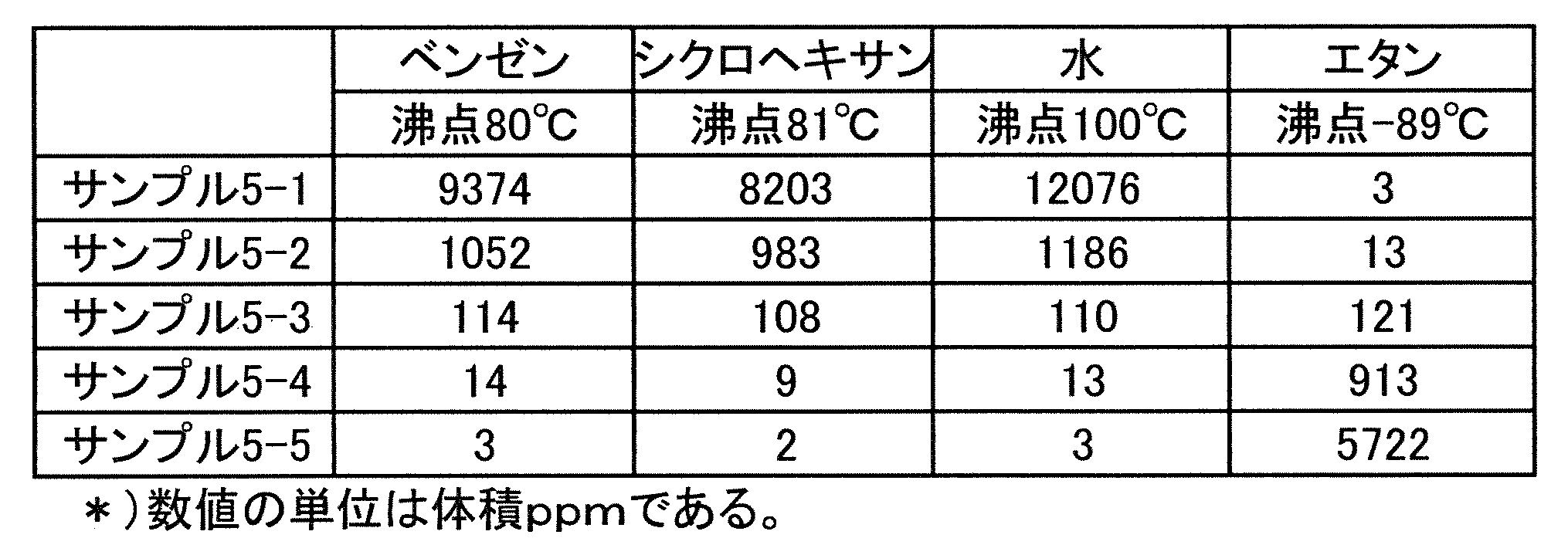
- Preparation Example 5 The same operation as in Preparation Example 1 was performed except that propylene (boiling point at a pressure of 101 kPa: -48 ° C.) was used as an etching compound and the liquefaction temperature was -45 ° C., Samples 5-1 to 5-5. -5 was prepared. Then, the concentrations of various impurities such as high-boiling impurities contained in each sample were measured by infrared spectroscopy and gas chromatography. Table 5 shows the results. The concentrations of impurities were measured by infrared spectroscopy for water, and by gas chromatography for benzene, cyclohexane, and ethane.
- Example 1 A silicon nitride film with a thickness of 1000 nm was formed on the surface of a semiconductor wafer, and a resist film with a thickness of 500 nm was further formed thereon. A hole having a diameter of 200 nm was formed in the resist film by performing exposure and development, and this was used as a test sample. Then, the specimen was etched using an etching gas. As an etching device, an ICP etching device RIE-230iP manufactured by Samco Corporation was used.
- an etching gas was prepared by introducing difluoromethane of sample 1-5 at a flow rate of 10 mL/min and argon at a flow rate of 40 mL/min into the chamber independently of each other and mixing them in the chamber.
- a high frequency voltage of 500 W was applied to convert the etching gas into plasma in the chamber.
- the test piece in the chamber was etched for 1 minute under etching conditions of a pressure of 3 Pa, a temperature of the test piece of ⁇ 50° C., and a bias power of 100 W.
- the temperature of the specimen was set to 20° C., and argon was introduced into the chamber at a flow rate of 40 mL/min to purge the surface of the specimen.
- Example 2 Etching of the specimen was carried out in the same manner as in Example 1, except that the temperature of the specimen was -5°C.
- Table 6 shows the etching rate of the silicon nitride film and the result of confirming whether or not bowing and etch stop occurred. As shown in Table 6, it was confirmed that etching progressed normally at an etching rate of 80 nm/min without bowing and etch stop.
- Example 3 A specimen was etched in the same manner as in Example 1, except that the difluoromethane of Sample 1-4 was used instead of the difluoromethane of Sample 1-5.
- Table 6 shows the etching rate of the silicon nitride film and the result of confirming whether or not bowing and etch stop occurred. As shown in Table 6, it was confirmed that the etching progressed normally at an etching rate of 87 nm/min without bowing or etch stop.
- Example 4 A specimen was etched in the same manner as in Example 1, except that the difluoromethane of Sample 1-3 was used instead of the difluoromethane of Sample 1-5.
- Table 6 shows the etching rate of the silicon nitride film and the result of confirming whether or not bowing and etch stop occurred. As shown in Table 6, it was confirmed that the etching progressed normally at an etching rate of 91 nm/min without bowing and etch stop.
- Example 1 A specimen was etched in the same manner as in Example 1, except that the difluoromethane of Sample 1-2 was used instead of the difluoromethane of Sample 1-5.
- Table 6 shows the etching rate of the silicon nitride film and the result of confirming whether or not bowing and etch stop occurred. As shown in Table 6, bowing was observed in the silicon nitride film immediately below the resist film to increase the diameter of the hole, confirming that etching in the lateral direction had progressed. The etching rate was 83 nm/min.
- Example 2 The same procedure as in Example 1 was performed except that the difluoromethane of Sample 1-1 was used instead of the difluoromethane of Sample 1-5 to etch the specimen.
- Table 6 shows the etching rate of the silicon nitride film and the result of confirming whether or not bowing and etch stop occurred. As shown in Table 6, bowing was observed in the silicon nitride film immediately below the resist film to increase the diameter of the hole, confirming that etching in the lateral direction had progressed. Also, the etching rate was 33 nm/min, and the occurrence of etch stop was confirmed.
- Example 4 Etching of the specimen was performed in the same manner as in Example 1, except that the temperature of the specimen was set to 25°C.
- Table 6 shows the etching rate of the silicon nitride film and the result of confirming whether or not bowing and etch stop occurred. As shown in Table 6, bowing was observed in the silicon nitride film immediately below the resist film to increase the diameter of the hole, confirming that etching in the lateral direction had progressed. The etching rate was 74 nm/min.
- Example 5 Example 1 except that a polysilicon film with a thickness of 1000 nm was formed instead of the silicon nitride film with a thickness of 1000 nm, and chlorine gas of sample 2-5 was used instead of difluoromethane of sample 1-5. Etching of the specimen was performed by performing the same operation. Table 6 shows the etching rate of the polysilicon film and the result of confirming whether or not bowing and etch stop occurred. As shown in Table 6, it was confirmed that etching progressed normally at an etching rate of 121 nm/min without bowing and etch stop.
- Example 6 The specimen was etched in the same manner as in Example 5, except that the chlorine gas of sample 2-4 was used instead of the chlorine gas of sample 2-5. Table 6 shows the etching rate of the polysilicon film and the result of confirming whether or not bowing and etch stop occurred. As shown in Table 6, it was confirmed that etching proceeded normally at an etching rate of 118 nm/min without occurrence of bowing and etch stop.
- Example 7 The specimen was etched in the same manner as in Example 5, except that the chlorine gas of sample 2-3 was used instead of the chlorine gas of sample 2-5.
- Table 6 shows the etching rate of the polysilicon film and the result of confirming whether or not bowing and etch stop occurred. As shown in Table 6, it was confirmed that etching proceeded normally at an etching rate of 119 nm/min without bowing or etch stop.
- Example 5 The specimen was etched in the same manner as in Example 5, except that the chlorine gas of sample 2-2 was used instead of the chlorine gas of sample 2-5.
- Table 6 shows the etching rate of the polysilicon film and the result of confirming whether or not bowing and etch stop occurred. As shown in Table 6, the etching rate was 47 nm/min, and the occurrence of etch stop was confirmed.
- Example 6 The specimen was etched in the same manner as in Example 5, except that the chlorine gas of sample 2-1 was used instead of the chlorine gas of sample 2-5.
- Table 6 shows the etching rate of the polysilicon film and the result of confirming whether or not bowing and etch stop occurred. As shown in Table 6, the etching rate was 32 nm/min, and the occurrence of etch stop was confirmed.
- Example 8 Example except that a polysilicon film with a thickness of 1000 nm was formed instead of the silicon nitride film with a thickness of 1000 nm, and hydrogen bromide of sample 3-5 was used instead of difluoromethane of sample 1-5. The same operation as in 1 was performed to etch the specimen. Table 6 shows the etching rate of the polysilicon film and the result of confirming whether or not bowing and etch stop occurred. As shown in Table 6, it was confirmed that the etching progressed normally at an etching rate of 63 nm/min without bowing or etch stop.
- Example 9 The specimen was etched in the same manner as in Example 8, except that the hydrogen bromide sample 3-4 was used instead of the hydrogen bromide sample 3-5.
- Table 6 shows the etching rate of the polysilicon film and the result of confirming whether or not bowing and etch stop occurred. As shown in Table 6, it was confirmed that etching proceeded normally at an etching rate of 67 nm/min without bowing or etch stop.
- Example 10 The specimen was etched in the same manner as in Example 8, except that the hydrogen bromide sample 3-3 was used instead of the hydrogen bromide sample 3-5.
- Table 6 shows the etching rate of the polysilicon film and the result of confirming whether or not bowing and etch stop occurred. As shown in Table 6, it was confirmed that etching progressed normally at an etching rate of 64 nm/min without bowing or etch stop.
- Example 7 Etching of the specimen was carried out in the same manner as in Example 8, except that the hydrogen bromide of sample 3-2 was used instead of the hydrogen bromide of sample 3-5.
- Table 6 shows the etching rate of the polysilicon film and the result of confirming whether or not bowing and etch stop occurred. As shown in Table 6, the etching rate was 28 nm/min, and the occurrence of etch stop was confirmed.
- Example 8 The specimen was etched in the same manner as in Example 8, except that the hydrogen bromide sample 3-1 was used instead of the hydrogen bromide sample 3-5.
- Table 6 shows the etching rate of the polysilicon film and the result of confirming whether or not bowing and etch stop occurred. As shown in Table 6, the etching rate was 21 nm/min, and the occurrence of etch stop was confirmed.
- Example 11 Except that a silicon oxide film with a thickness of 1000 nm was formed instead of the silicon nitride film with a thickness of 1000 nm, and trifluoroiodomethane of sample 4-5 was used instead of difluoromethane of sample 1-5.
- Table 6 shows the etching rate of the silicon oxide film and the result of confirming whether or not bowing and etch stop occurred. As shown in Table 6, it was confirmed that the etching progressed normally at an etching rate of 71 nm/min without bowing or etch stop.
- Example 12 Etching of the specimen was carried out in the same manner as in Example 11, except that the trifluoroiodomethane of sample 4-4 was used instead of the trifluoroiodomethane of sample 4-5.
- Table 6 shows the etching rate of the silicon oxide film and the result of confirming whether or not bowing and etch stop occurred. As shown in Table 6, it was confirmed that etching proceeded normally at an etching rate of 74 nm/min without bowing or etch stop.
- Example 13 The same operation as in Example 11 was performed except that the trifluoroiodomethane of Sample 4-3 was used instead of the trifluoroiodomethane of 4-5 to etch the specimen.
- Table 6 shows the etching rate of the silicon oxide film and the result of confirming whether or not bowing and etch stop occurred. As shown in Table 6, it was confirmed that etching progressed normally at an etching rate of 81 nm/min without bowing or etch stop.
- Example 9 The same procedure as in Example 11 was performed except that the trifluoroiodomethane of Sample 4-2 was used instead of the trifluoroiodomethane of 4-5 to etch the specimen.
- Table 6 shows the etching rate of the silicon oxide film and the result of confirming whether or not bowing and etch stop occurred. As shown in Table 6, bowing was observed in the silicon oxide film immediately below the resist film to increase the diameter of the hole, confirming that etching in the lateral direction had progressed. Also, the etching rate was 33 nm/min, and the occurrence of etch stop was confirmed.
- Example 10 The same operation as in Example 11 was performed except that the trifluoroiodomethane of sample 4-1 was used instead of the trifluoroiodomethane of 4-5 to etch the specimen.
- Table 6 shows the etching rate of the silicon oxide film and the result of confirming whether or not bowing and etch stop occurred. As shown in Table 6, bowing was observed in the silicon oxide film immediately below the resist film to increase the diameter of the hole, confirming that etching in the lateral direction had progressed. Also, the etching rate was 18 nm/min, and the occurrence of etch stop was confirmed.
- Example 14 The same operation as in Example 1 was performed except that a mixture of propylene of sample 5-5 and tetrafluoromethane with a purity of 99.99% by volume was used instead of difluoromethane of sample 1-5. Etching the body. Specifically, propylene of sample 5-5 was introduced into the chamber at a flow rate of 10 mL/min, tetrafluoromethane at a flow rate of 10 mL/min, and argon at a flow rate of 30 mL/min, respectively, and mixed in the chamber. An etching gas was prepared. Table 6 shows the etching rate of the silicon nitride film and the result of confirming whether or not bowing and etch stop occurred. As shown in Table 6, it was confirmed that the etching proceeded normally at an etching rate of 137 nm/min without bowing or etch stop.
- Example 15 A specimen was etched in the same manner as in Example 14, except that the propylene of Sample 5-4 was used instead of the propylene of Sample 5-5.
- Table 6 shows the etching rate of the silicon nitride film and the result of confirming whether or not bowing and etch stop occurred. As shown in Table 6, it was confirmed that the etching progressed normally at an etching rate of 133 nm/min without bowing and etch stop.
- Example 16 A specimen was etched in the same manner as in Example 14, except that the propylene of Sample 5-3 was used instead of the propylene of Sample 5-5.
- Table 6 shows the etching rate of the silicon nitride film and the result of confirming whether or not bowing and etch stop occurred. As shown in Table 6, it was confirmed that the etching proceeded normally at an etching rate of 134 nm/min without bowing or etch stop.
- Example 11 A specimen was etched in the same manner as in Example 14 except that the propylene of Sample 5-2 was used instead of the propylene of Sample 5-5.
- Table 6 shows the etching rate of the silicon nitride film and the result of confirming whether or not bowing and etch stop occurred. As shown in Table 6, the etching rate was 42 nm/min, and the occurrence of etch stop was confirmed.
- Example 12 A specimen was etched in the same manner as in Example 14, except that the propylene of Sample 5-1 was used instead of the propylene of Sample 5-5.
- Table 6 shows the etching rate of the silicon nitride film and the result of confirming whether or not bowing and etch stop occurred. As shown in Table 6, the etching rate was 39 nm/min, and the occurrence of etch stop was confirmed.
Landscapes
- Chemical & Material Sciences (AREA)
- Engineering & Computer Science (AREA)
- Materials Engineering (AREA)
- Organic Chemistry (AREA)
- Drying Of Semiconductors (AREA)
- Physics & Mathematics (AREA)
- Plasma & Fusion (AREA)
Abstract
Description
エッチングガスには不純物(例えば、エッチングガスの製造工程に由来する不純物)が混入するおそれがあり、混入した不純物はエッチング時に凝縮して、エッチング速度及びエッチングの選択性を低下させるおそれがあった。
本発明は、ボーイング及びエッチストップが発生しにくい低温エッチング方法を提供することを課題とする。
[1] ケイ素を含有するエッチング対象物を有する被エッチング部材の温度を0℃以下にし、エッチング化合物を含有するエッチングガスを前記被エッチング部材に接触させて、前記エッチング対象物をエッチングするエッチング工程を備え、
前記エッチングガスは、フッ素原子、塩素原子、臭素原子、ヨウ素原子、水素原子、及び酸素原子のうち少なくとも1種の原子を分子内に有し且つ101kPaの圧力下での沸点が20℃以上である化合物である高沸点不純物を含有するか又は含有せず、前記高沸点不純物を含有する場合は、含有する全種の前記高沸点不純物の濃度の総和が500体積ppm以下であるエッチング方法。
[3] 前記高沸点不純物が、水、フッ化水素、エタノール、イソプロパノール、クロロホルム、ジクロロメタン、シクロヘキサン、ベンゼン、ヨウ素分子、及び臭素分子のうち少なくとも1種である[1]又は[2]に記載のエッチング方法。
[4] 前記エッチング化合物は、フッ素原子、塩素原子、臭素原子、ヨウ素原子、及び水素原子のうち少なくとも1種の原子を分子内に有し且つ101kPaの圧力下での沸点が15℃以下である化合物である[1]~[3]のいずれか一項に記載のエッチング方法。
[7] 前記エッチング化合物が、臭素原子を分子内に有する化合物であり、臭化水素、炭素数1以上3以下の鎖状飽和臭素化炭化水素、及び炭素数2の不飽和臭素化炭化水素のうち少なくとも1種である[4]に記載のエッチング方法。
[9] 前記エッチング化合物が、水素原子を分子内に有する化合物であり、炭素数1以上4以下の鎖状飽和炭化水素、炭素数2以上4以下の不飽和炭化水素、及び炭素数3又は4の環状炭化水素のうち少なくとも1種である[4]に記載のエッチング方法。
なお、高沸点不純物及びエッチング化合物の沸点は、101kPaの圧力下での沸点(すなわち、大気圧下での沸点)であるが、これ以降の記載では、単に「沸点」と記すこともある。
よって、本実施形態に係るエッチング方法は、半導体素子の製造に利用することができる。例えば、ケイ素化合物からなる薄膜を有する半導体基板に対して、本実施形態に係るエッチング方法を適用し、ケイ素化合物からなる薄膜のエッチングを行えば、半導体素子を製造することができる。本実施形態に係るエッチング方法は、エッチング速度及びエッチングの選択性が高いので、半導体素子の生産性が高い。
〔エッチング方法〕
本実施形態に係るエッチング方法には、プラズマを使用するプラズマエッチング、プラズマを使用しないプラズマレスエッチングのいずれも用いることができる。プラズマエッチングとしては、例えば、反応性イオンエッチング(RIE:Reactive Ion Etching)、誘導結合型プラズマ(ICP:Inductively Coupled Plasma)エッチング、容量結合型プラズマ(CCP:Capacitively Coupled Plasma)エッチング、電子サイクロトロン共鳴(ECR:Electron Cyclotron Resonance)プラズマエッチング、マイクロ波プラズマエッチングが挙げられる。
また、プラズマエッチングにおいては、プラズマは被エッチング部材が設置されたチャンバー内で発生させてもよいし、プラズマ発生室と被エッチング部材を設置するチャンバーとを分けてもよい(すなわち、遠隔プラズマを用いてもよい)。遠隔プラズマを用いたエッチングにより、ケイ素を含有するエッチング対象物をより高い選択性でエッチングできる場合がある。
エッチングガスに含有されるエッチング化合物は、ケイ素を含有するエッチング対象物と反応して、エッチング対象物のエッチングを進行させる化合物である。エッチング化合物は、エッチング対象物のエッチングを進行させる化合物であれば、その種類は特に限定されるものではないが、フッ素原子、塩素原子、臭素原子、ヨウ素原子、及び水素原子のうち少なくとも1種の原子を分子内に有し且つ101kPaの圧力下での沸点が15℃以下である化合物であることが好ましい。
エッチング化合物の101kPaの圧力下での沸点は、15℃以下であることが好ましいが、10℃以下であることがより好ましく、0℃以下であることがさらに好ましい。エッチング化合物の例を以下に示す。
炭素数1以上3以下の鎖状飽和ハイドロフルオロカーボンの具体例としては、フルオロメタン(CH3F)、ジフルオロメタン(CH2F2)、トリフルオロメタン(CHF3)、フルオロエタン(C2H5F)、ジフルオロエタン(C2H4F2)、トリフルオロエタン(C2H3F3)、テトラフルオロエタン(C2H2F4)、ペンタフルオロエタン(C2HF5)、フルオロプロパン(C3H7F)、ジフルオロプロパン(C3H6F2)、トリフルオロプロパン(C3H5F3)、テトラフルオロプロパン(C3H4F4)、ペンタフルオロプロパン(C3H3F5)、ヘキサフルオロプロパン(C3H2F6)、ヘプタフルオロプロパン(C3HF7)が挙げられる。
炭素数2以上4以下の不飽和ハイドロフルオロカーボンの具体例としては、フルオロエチレン(C2H3F)、ジフルオロエチレン(C2H2F2)、トリフルオロエチレン(C2HF3)、フルオロプロピレン(C3H5F)、ジフルオロプロピレン(C3H4F2)、トリフルオロプロピレン(C3H3F3)、テトラフルオロプロピレン(C3H2F4)、ペンタフルオロプロピレン(C3HF5)、フルオロプロピン(C3H3F)、ジフルオロプロピン(C3H2F2)、トリフルオロプロピン(C3HF3)、ジフルオロブテン(C4H6F2)、トリフルオロブテン(C4H5F3)、ペンタフルオロブテン(C4H3F5)、ヘキサフルオロブテン(C4H2F6)、ヘプタフルオロブテン(C4HF7)、フルオロブチン(C4H5F)、ジフルオロブチン(C4H4F2)、トリフルオロブチン(C4H3F3)、テトラフルオロブチン(C4H2F4)、ペンタフルオロブチン(C4HF5)が挙げられる。
炭素数3以上5以下の環状ハイドロフルオロカーボンの具体例としては、フルオロシクロプロパン(C3H5F)、ジフルオロシクロプロパン(C3H4F2)、トリフルオロシクロプロパン(C3H3F3)、テトラフルオロシクロプロパン(C3H2F4)、ペンタフルオロシクロプロパン(C3HF5)、ヘプタフルオロシクロブタン(C4HF7)が挙げられる。
なお、本発明においては、ハイドロフルオロカーボンとは、炭化水素が有する水素原子の一部がフッ素原子で置換された化合物を意味する。
炭素数1以上3以下の鎖状飽和臭素化炭化水素の具体例としては、ブロモメタン(CH3Br)、ブロモジフルオロメタン(CHBrF2)、ブロモフルオロメタン(CH2BrF)、ブロモトリフルオロメタン(CBrF3)、ブロモテトラフルオロエタン(C2HBrF4)、ブロモペンタフルオロエタン(C2BrF5)、ブロモヘプタフルオロプロパン(C3BrF7)が挙げられる。
ヨウ素原子を分子内に有するエッチング化合物の例としては、七フッ化ヨウ素、ヨウ化水素(HI)、トリフルオロヨードメタン、及びペンタフルオロヨードエタン(C2F5I)が挙げられる。
水素原子を分子内に有するエッチング化合物の例としては、炭素数1以上4以下の鎖状飽和炭化水素、炭素数2以上4以下の不飽和炭化水素、及び炭素数3又は4の環状炭化水素が挙げられる。
炭素数1以上4以下の鎖状飽和炭化水素の具体例としては、メタン(CH4)、エタン(C2H6)、プロパン(C3H8)、ブタン(C4H10)が挙げられる。
炭素数3又は4の環状炭化水素の具体例としては、シクロプロパン(C3H6)、シクロブタン(C4H8)、シクロブテン(C4H6)が挙げられる。
これらのエッチング化合物は、1種を単独で使用してもよいし、2種以上を組み合わせて使用してもよい。なお、具体例として上記に示したエッチング化合物の一部には、異性体が存在するものがあるが、いずれの異性体も、本実施形態に係るエッチング方法におけるエッチング化合物として使用することができる。
エッチングガスは、上記エッチング化合物を含有するガスである。エッチングガスは、上記エッチング化合物のみからなるガスであってもよいし、上記エッチング化合物と希釈ガスを含有する混合ガスであってもよい。また、上記エッチング化合物と希釈ガスと添加ガスを含有する混合ガスであってもよい。
希釈ガスの種類は、不活性ガスであれば特に限定されるものではないが、例えば、窒素ガス(N2)、ヘリウム(He)、ネオン(Ne)、アルゴン(Ar)、クリプトン(Kr)、及びキセノン(Xe)から選ばれる少なくとも1種を用いることができる。
エッチングガス中のエッチング化合物の含有量は、エッチング速度を向上させる観点から、エッチングガスの総量に対して5体積%以上が好ましく、10体積%以上がより好ましい。また、エッチング化合物の使用量を抑制する観点から、エッチングガスの総量に対して90体積%以下が好ましく、80体積%以下がより好ましい。
エッチングガスは、高沸点不純物を含有するか又は含有しないが、高沸点不純物を含有する場合は、含有する全種の高沸点不純物の濃度の総和が、ガス化したエッチングガスの総量に対して500体積ppm以下であるため、前述したように高沸点不純物の凝縮に起因する不具合が生じにくく、エッチング速度及びエッチングの選択性が高い。エッチングガスが含有する全種の高沸点不純物の濃度の総和は、0.01体積ppm以上300体積ppm以下であってもよい。また、エッチングガスが含有する全種の高沸点不純物の各濃度は、いずれも0.01体積ppm以上であってもよい。
なお、本発明においては、高沸点不純物とは、フッ素原子、塩素原子、臭素原子、ヨウ素原子、水素原子、及び酸素原子のうち少なくとも1種の原子を分子内に有し且つ101kPaの圧力下での沸点が20℃以上である化合物である。エッチングガス又はエッチング化合物には、1種又は複数種の高沸点不純物が含有されている場合がある。
エッチングガス又はエッチング化合物から高沸点不純物を除去する方法としては、例えば、吸着剤と接触させる方法、膜で分離する方法、蒸留で分離する方法等が挙げられる。蒸留で分離する方法の具体例を示すと、ステンレス製シリンダーにエッチングガス又はエッチング化合物を封入して、シリンダー内圧下でのエッチング化合物の沸点以下の温度に保持した状態で(例えばエッチング化合物がジフルオロメタンである場合は、1気圧よりやや高めのシリンダー内圧下で-50℃に保持した状態で)、後述の実施例に記載する方法等によって気相部を抜き出すことで、高沸点不純物を分離することができる。このような高沸点不純物を除去する工程によって、エッチングガスが含有する高沸点不純物の濃度の総和を500体積ppm以下とした後に、エッチングガスをエッチングに供するとよい。
沸点が20℃以上60℃未満の高沸点不純物の濃度の総和は、ガス化したエッチングガスの総量に対して500体積ppm以下である必要があり、50体積ppm以下であることが好ましく、1体積ppm以下であることがより好ましい。沸点が20℃以上60℃未満の高沸点不純物の濃度の総和は、0.01体積ppm以上であってもよい。
沸点が20℃以上60℃未満の高沸点不純物の種類は特に限定されるものではないが、例えば、フッ化水素(HF、沸点20℃)、臭素分子(Br2、沸点58.8℃)、ジクロロメタン(CH2Cl2、沸点40℃)、トリクロロトリフルオロエタン(C2Cl3F3、沸点47.7℃)、ジクロロトリフルオロエタン(C2HCl2F3、沸点27.8℃)、ジクロロフルオロエタン(C2H3Cl2F、沸点32℃)、ヨードメタン(CH3I、沸点42.4℃)、二酸化窒素(NO2、沸点21.1℃)が挙げられる。
沸点が60℃以上100℃未満の高沸点不純物の種類は特に限定されるものではないが、例えば、エタノール(CH3CH2OH、沸点78℃)、イソプロパノール(C3H7OH、沸点82.4℃)、クロロホルム(CHCl3、沸点61.2℃)、テトラクロロジフルオロエタン(C2Cl4F2、沸点92.8℃)、ベンゼン(C6H6、沸点80℃)、シクロヘキサン(C6H12、沸点81℃)、ヘキサフルオロベンゼン(C6F6、沸点80.5℃)、テトラクロロエチレン(C2Cl4、沸点87.2℃)、三塩化リン(PCl3、沸点74℃)が挙げられる。
沸点が100℃以上200℃未満の高沸点不純物の種類は特に限定されるものではないが、例えば、水(H2O、沸点100℃)、ヨウ素分子(I2、沸点184.3℃)、四臭化炭素(CBr4、沸点190℃)、トリブロモフルオロメタン(CBr3F、沸点108℃)、五フッ化ヨウ素(IF5、沸点104℃)、三臭化リン(PBr3、沸点173.2℃)が挙げられる。
なお、エッチングガスには、沸点が20℃未満の化合物が不純物として含有されていてもよい。沸点が20℃未満の不純物の濃度の総和は、ガス化したエッチングガスの総量に対して1000体積ppm以下であることが好ましく、50体積ppm以下であることがより好ましく、1体積ppm以下であることがさらに好ましい。沸点が20℃未満の不純物の濃度の総和は、0.01体積ppm以上であってもよい。
本実施形態に係るエッチング方法は低温エッチングであるので、被エッチング部材の温度を0℃以下にしてエッチングを行うが、被エッチング部材の温度は-20℃以下とすることが好ましく、-40℃以下とすることがより好ましい。被エッチング部材の温度を上記範囲内としてエッチングを行えば、より低いサイドエッチ率でエッチングを行うことができる。
ここで、温度条件の温度とは、被エッチング部材の温度であるが、エッチング装置のチャンバー内に設置された、被エッチング部材を支持するステージの温度を使用することもできる。
エッチングを行う際に発生させるプラズマと被エッチング部材との間の電位差を構成するバイアスパワーについては、所望するエッチング形状により0~10000Wから選択すればよく、選択的にエッチングを行う場合は0~1000W程度が好ましい。
本実施形態に係るエッチング方法におけるエッチング工程の圧力条件は特に限定されるものではないが、10Pa以下とすることが好ましく、5Pa以下とすることがより好ましい。圧力条件が上記の範囲内であれば、プラズマを安定して発生させやすい。一方、エッチング工程の圧力条件は0.05Pa以上であることが好ましい。圧力条件が上記の範囲内であれば、電離イオンが多く発生し十分なプラズマ密度が得られやすい。
エッチングガスの流量は、チャンバーの容積やチャンバー内を減圧する排気設備の能力に応じて、チャンバー内の圧力が一定に保たれるように適宜設定すればよい。
本実施形態に係るエッチング方法によりエッチングする被エッチング部材は、エッチングの対象であるエッチング対象物を有するが、エッチングの対象ではない非エッチング対象物をさらに有していてもよい。
被エッチング部材がエッチング対象物と非エッチング対象物を有する場合は、被エッチング部材は、エッチング対象物で形成されている部分と非エッチング対象物で形成されている部分とを有する部材でもよいし、エッチング対象物と非エッチング対象物の混合物で形成されている部材でもよい。また、被エッチング部材は、エッチング対象物、非エッチング対象物以外のものを有していてもよい。
また、被エッチング部材の形状は特に限定されるものではなく、例えば、板状、箔状、膜状、粉末状、塊状であってもよい。被エッチング部材の例としては、前述した半導体基板が挙げられる。
エッチング対象物は、ケイ素を含有する材料のみで形成されているものであってもよいし、ケイ素を含有する材料のみで形成されている部分と他の材質で形成されている部分とを有するものであってもよいし、ケイ素を含有する材料と他の材質の混合物で形成されているものであってもよい。ケイ素を含有する材料としては、例えば、酸化ケイ素、窒化ケイ素、ポリシリコン、シリコンゲルマニウム(SiGe)が挙げられる。これらのケイ素を含有する材料は、1種を単独で使用してもよいし、2種以上を組み合わせて使用してもよい。
また、エッチング対象物の形状は、特に限定されるものではなく、例えば、板状、箔状、膜状、粉末状、塊状であってもよい。さらに、エッチング対象物には、パターンやホール等の形状が形成されていてもよいし、形成されていなくてもよい。
非エッチング対象物は、上記エッチング化合物と実質的に反応しないか、又は、上記エッチング化合物との反応が極めて遅いため、本実施形態に係るエッチング方法によりエッチングを行っても、エッチングがほとんど進行しないものである。非エッチング対象物は、上記のような性質を有するならば特に限定されるものではないが、例えば、フォトレジスト、アモルファスカーボン、窒化チタンや、銅、ニッケル、コバルト等の金属や、これら金属の酸化物、窒化物が挙げられる。これらの中でも、取扱性及び入手容易性の観点から、フォトレジスト、アモルファスカーボンがより好ましい。
プラズマ発生装置のプラズマ生成機構の種類は特に限定されるものではなく、平行板に高周波電圧をかけるものであってもよいし、コイルに高周波電流を流すものであってもよい。プラズマ中で被エッチング部材4に高周波電圧をかけると被エッチング部材4に負の電圧がかかり、プラスイオンが被エッチング部材4に高速且つ垂直に入射するので、異方性エッチングが可能となる。図1のエッチング装置においては、ステージ5とプラズマ発生装置の高周波電源とが接続されていて、ステージ5に高周波電圧を印加することができるようになっている。
また、エッチングガスとしてエッチング化合物ガスと不活性ガス等の希釈ガスとの混合ガスを使用する場合には、チャンバー3の内部を真空ポンプ8で減圧した上で、エッチング化合物ガス供給部1からエッチング化合物ガスを送り出すとともに、希釈ガス供給部2から希釈ガスを送り出せばよい。これにより、チャンバー3内においてエッチング化合物ガスと希釈ガスが混合されてエッチングガスとなる。
例えば、チャンバー3の温度調節機構の構成は、被エッチング部材4の温度を任意の温度に調節できればよいので、図1のエッチング装置のように外付けの冷却部6でチャンバー3の外側からステージ5を冷却する構成でもよいし、ステージ5を冷却する冷却部をステージ5上に直接備える構成でもよい。
マンガン鋼製の容量1Lのシリンダー(密閉可能な円筒型容器)を5個用意した。それらシリンダーを順に、シリンダーA、シリンダーB、シリンダーC、シリンダーD、シリンダーEと呼ぶ。シリンダーAにはジフルオロメタン(圧力101kPaでの沸点:-52℃)500gを充填し、-50℃に冷却することにより液化させ、100kPaよりもやや高い圧力状態で液相部と気相部とを形成させた。シリンダーB、C、D、Eは、真空ポンプで内部を1kPa以下に減圧した後に-196℃に冷却した。

また、シリンダーE内のジフルオロメタン100gを、サンプル1-5とする。シリンダーEの気相部が存在している上側出口からジフルオロメタンのガスを抜き出し、赤外分光分析法とガスクロマトグラフィー法で高沸点不純物等の各種不純物の濃度を測定した。結果を表1に示す。
エッチング化合物として塩素ガス(圧力101kPaでの沸点:-34℃)を使用した点と、液化温度を-30℃とした点以外は、調製例1と同様の操作を行って、サンプル2-1~2-5を調製した。そして、それぞれのサンプルに含有される高沸点不純物等の各種不純物の濃度を赤外分光分析法とガスクロマトグラフィー法で測定した。結果を表2に示す。なお、不純物の濃度の測定は、塩化水素と水については赤外分光分析法で、ジクロロメタンとクロロホルムについてはガスクロマトグラフィー法で行った。

エッチング化合物として臭化水素(圧力101kPaでの沸点:-66℃)を使用した点と、液化温度を-60℃とした点以外は、調製例1と同様の操作を行って、サンプル3-1~3-5を調製した。そして、それぞれのサンプルに含有される高沸点不純物等の各種不純物の濃度を赤外分光分析法とガスクロマトグラフィー法と質量分析法で測定した。結果を表3に示す。なお、不純物の濃度の測定は、水については赤外分光分析法で、二酸化炭素についてはガスクロマトグラフィー法で、臭素分子については質量分析法で行った。

エッチング化合物としてトリフルオロヨードメタン(圧力101kPaでの沸点:-23℃)を使用した点と、液化温度を-20℃とした点以外は、調製例1と同様の操作を行って、サンプル4-1~4-5を調製した。そして、それぞれのサンプルに含有される高沸点不純物等の各種不純物の濃度を赤外分光分析法と質量分析法で測定した。結果を表4に示す。なお、不純物の濃度の測定は、水、フッ化水素、ヨウ化水素については赤外分光分析法で、ヨウ素分子については質量分析法で行った。

エッチング化合物としてプロピレン(圧力101kPaでの沸点:-48℃)を使用した点と、液化温度を-45℃とした点以外は、調製例1と同様の操作を行って、サンプル5-1~5-5を調製した。そして、それぞれのサンプルに含有される高沸点不純物等の各種不純物の濃度を赤外分光分析法とガスクロマトグラフィー法で測定した。結果を表5に示す。なお、不純物の濃度の測定は、水については赤外分光分析法で、ベンゼン、シクロヘキサン、エタンについてはガスクロマトグラフィー法で行った。
半導体ウエハの表面上に、厚さ1000nmの窒化ケイ素膜を形成し、さらにその上に厚さ500nmのレジスト膜を形成した。露光及び現像を行うことによりレジスト膜に直径200nmのホールを形成して、これを試験体とした。そして、エッチングガスを用いて試験体のエッチングを行った。
エッチング装置としては、サムコ株式会社製のICPエッチング装置RIE-230iPを使用した。具体的には、サンプル1-5のジフルオロメタンを流量10mL/minで、アルゴンを流量40mL/minでそれぞれ独立してチャンバー内に導入して、チャンバー内で混合しエッチングガスを調製した。
エッチングが終了したら、試験体の温度を20℃とするとともに、アルゴンを流量40mL/minでチャンバー内に導入して、試験体の表面をパージした。

試験体の温度を-5℃とした点以外は、実施例1と同様の操作を行って、試験体のエッチングを行った。窒化ケイ素膜のエッチング速度と、ボーイング及びエッチストップが発生したか否かの確認結果を、表6に示す。表6に示すように、ボーイング及びエッチストップが発生することなく、エッチング速度80nm/minで正常にエッチングが進行したことが確認された。
試験体の温度を25℃とした点以外は、実施例1と同様の操作を行って、試験体のエッチングを行った。窒化ケイ素膜のエッチング速度と、ボーイング及びエッチストップが発生したか否かの確認結果を、表6に示す。表6に示すように、ボーイング及びエッチストップが発生することなく、エッチング速度79nm/minで正常にエッチングが進行したことが確認された。
サンプル1-5のジフルオロメタンの代わりにサンプル1-4のジフルオロメタンを使用した点以外は、実施例1と同様の操作を行って、試験体のエッチングを行った。窒化ケイ素膜のエッチング速度と、ボーイング及びエッチストップが発生したか否かの確認結果を、表6に示す。表6に示すように、ボーイング及びエッチストップが発生することなく、エッチング速度87nm/minで正常にエッチングが進行したことが確認された。
サンプル1-5のジフルオロメタンの代わりにサンプル1-3のジフルオロメタンを使用した点以外は、実施例1と同様の操作を行って、試験体のエッチングを行った。窒化ケイ素膜のエッチング速度と、ボーイング及びエッチストップが発生したか否かの確認結果を、表6に示す。表6に示すように、ボーイング及びエッチストップが発生することなく、エッチング速度91nm/minで正常にエッチングが進行したことが確認された。
サンプル1-5のジフルオロメタンの代わりにサンプル1-2のジフルオロメタンを使用した点以外は、実施例1と同様の操作を行って、試験体のエッチングを行った。窒化ケイ素膜のエッチング速度と、ボーイング及びエッチストップが発生したか否かの確認結果を、表6に示す。表6に示すように、窒化ケイ素膜のうちレジスト膜の直下部で穴の直径が大きくなるボーイングの発生が観測され、横方向のエッチングが進行したことが確認された。エッチング速度は83nm/minであった。
サンプル1-5のジフルオロメタンの代わりにサンプル1-1のジフルオロメタンを使用した点以外は、実施例1と同様の操作を行って、試験体のエッチングを行った。窒化ケイ素膜のエッチング速度と、ボーイング及びエッチストップが発生したか否かの確認結果を、表6に示す。表6に示すように、窒化ケイ素膜のうちレジスト膜の直下部で穴の直径が大きくなるボーイングの発生が観測され、横方向のエッチングが進行したことが確認された。また、エッチング速度は33nm/minで、エッチストップの発生が確認された。
試験体の温度を-5℃とした点以外は、実施例1と同様の操作を行って、試験体のエッチングを行った。窒化ケイ素膜のエッチング速度と、ボーイング及びエッチストップが発生したか否かの確認結果を、表6に示す。表6に示すように、窒化ケイ素膜のうちレジスト膜の直下部で穴の直径が大きくなるボーイングの発生が観測され、横方向のエッチングが進行したことが確認された。エッチング速度は81nm/minであった。
試験体の温度を25℃とした点以外は、実施例1と同様の操作を行って、試験体のエッチングを行った。窒化ケイ素膜のエッチング速度と、ボーイング及びエッチストップが発生したか否かの確認結果を、表6に示す。表6に示すように、窒化ケイ素膜のうちレジスト膜の直下部で穴の直径が大きくなるボーイングの発生が観測され、横方向のエッチングが進行したことが確認された。エッチング速度は74nm/minであった。
厚さ1000nmの窒化ケイ素膜の代わりに厚さ1000nmのポリシリコン膜を形成した点と、サンプル1-5のジフルオロメタンの代わりにサンプル2-5の塩素ガスを使用した点以外は、実施例1と同様の操作を行って、試験体のエッチングを行った。ポリシリコン膜のエッチング速度と、ボーイング及びエッチストップが発生したか否かの確認結果を、表6に示す。表6に示すように、ボーイング及びエッチストップが発生することなく、エッチング速度121nm/minで正常にエッチングが進行したことが確認された。
2-5の塩素ガスの代わりにサンプル2-4の塩素ガスを使用した点以外は、実施例5と同様の操作を行って、試験体のエッチングを行った。ポリシリコン膜のエッチング速度と、ボーイング及びエッチストップが発生したか否かの確認結果を、表6に示す。表6に示すように、ボーイング及びエッチストップが発生することなく、エッチング速度118nm/minで正常にエッチングが進行したことが確認された。
2-5の塩素ガスの代わりにサンプル2-3の塩素ガスを使用した点以外は、実施例5と同様の操作を行って、試験体のエッチングを行った。ポリシリコン膜のエッチング速度と、ボーイング及びエッチストップが発生したか否かの確認結果を、表6に示す。表6に示すように、ボーイング及びエッチストップが発生することなく、エッチング速度119nm/minで正常にエッチングが進行したことが確認された。
2-5の塩素ガスの代わりにサンプル2-2の塩素ガスを使用した点以外は、実施例5と同様の操作を行って、試験体のエッチングを行った。ポリシリコン膜のエッチング速度と、ボーイング及びエッチストップが発生したか否かの確認結果を、表6に示す。表6に示すように、エッチング速度は47nm/minで、エッチストップの発生が確認された。
2-5の塩素ガスの代わりにサンプル2-1の塩素ガスを使用した点以外は、実施例5と同様の操作を行って、試験体のエッチングを行った。ポリシリコン膜のエッチング速度と、ボーイング及びエッチストップが発生したか否かの確認結果を、表6に示す。表6に示すように、エッチング速度は32nm/minで、エッチストップの発生が確認された。
厚さ1000nmの窒化ケイ素膜の代わりに厚さ1000nmのポリシリコン膜を形成した点と、サンプル1-5のジフルオロメタンの代わりにサンプル3-5の臭化水素を使用した点以外は、実施例1と同様の操作を行って、試験体のエッチングを行った。ポリシリコン膜のエッチング速度と、ボーイング及びエッチストップが発生したか否かの確認結果を、表6に示す。表6に示すように、ボーイング及びエッチストップが発生することなく、エッチング速度63nm/minで正常にエッチングが進行したことが確認された。
3-5の臭化水素の代わりにサンプル3-4の臭化水素を使用した点以外は、実施例8と同様の操作を行って、試験体のエッチングを行った。ポリシリコン膜のエッチング速度と、ボーイング及びエッチストップが発生したか否かの確認結果を、表6に示す。表6に示すように、ボーイング及びエッチストップが発生することなく、エッチング速度67nm/minで正常にエッチングが進行したことが確認された。
3-5の臭化水素の代わりにサンプル3-3の臭化水素を使用した点以外は、実施例8と同様の操作を行って、試験体のエッチングを行った。ポリシリコン膜のエッチング速度と、ボーイング及びエッチストップが発生したか否かの確認結果を、表6に示す。表6に示すように、ボーイング及びエッチストップが発生することなく、エッチング速度64nm/minで正常にエッチングが進行したことが確認された。
3-5の臭化水素の代わりにサンプル3-2の臭化水素を使用した点以外は、実施例8と同様の操作を行って、試験体のエッチングを行った。ポリシリコン膜のエッチング速度と、ボーイング及びエッチストップが発生したか否かの確認結果を、表6に示す。表6に示すように、エッチング速度は28nm/minで、エッチストップの発生が確認された。
3-5の臭化水素の代わりにサンプル3-1の臭化水素を使用した点以外は、実施例8と同様の操作を行って、試験体のエッチングを行った。ポリシリコン膜のエッチング速度と、ボーイング及びエッチストップが発生したか否かの確認結果を、表6に示す。表6に示すように、エッチング速度は21nm/minで、エッチストップの発生が確認された。
厚さ1000nmの窒化ケイ素膜の代わりに厚さ1000nmの酸化ケイ素膜を形成した点と、サンプル1-5のジフルオロメタンの代わりにサンプル4-5のトリフルオロヨードメタンを使用した点以外は、実施例1と同様の操作を行って、試験体のエッチングを行った。酸化ケイ素膜のエッチング速度と、ボーイング及びエッチストップが発生したか否かの確認結果を、表6に示す。表6に示すように、ボーイング及びエッチストップが発生することなく、エッチング速度71nm/minで正常にエッチングが進行したことが確認された。
4-5のトリフルオロヨードメタンの代わりにサンプル4-4のトリフルオロヨードメタンを使用した点以外は、実施例11と同様の操作を行って、試験体のエッチングを行った。酸化ケイ素膜のエッチング速度と、ボーイング及びエッチストップが発生したか否かの確認結果を、表6に示す。表6に示すように、ボーイング及びエッチストップが発生することなく、エッチング速度74nm/minで正常にエッチングが進行したことが確認された。
4-5のトリフルオロヨードメタンの代わりにサンプル4-3のトリフルオロヨードメタンを使用した点以外は、実施例11と同様の操作を行って、試験体のエッチングを行った。酸化ケイ素膜のエッチング速度と、ボーイング及びエッチストップが発生したか否かの確認結果を、表6に示す。表6に示すように、ボーイング及びエッチストップが発生することなく、エッチング速度81nm/minで正常にエッチングが進行したことが確認された。
4-5のトリフルオロヨードメタンの代わりにサンプル4-2のトリフルオロヨードメタンを使用した点以外は、実施例11と同様の操作を行って、試験体のエッチングを行った。酸化ケイ素膜のエッチング速度と、ボーイング及びエッチストップが発生したか否かの確認結果を、表6に示す。表6に示すように、酸化ケイ素膜のうちレジスト膜の直下部で穴の直径が大きくなるボーイングの発生が観測され、横方向のエッチングが進行したことが確認された。また、エッチング速度は33nm/minで、エッチストップの発生が確認された。
4-5のトリフルオロヨードメタンの代わりにサンプル4-1のトリフルオロヨードメタンを使用した点以外は、実施例11と同様の操作を行って、試験体のエッチングを行った。酸化ケイ素膜のエッチング速度と、ボーイング及びエッチストップが発生したか否かの確認結果を、表6に示す。表6に示すように、酸化ケイ素膜のうちレジスト膜の直下部で穴の直径が大きくなるボーイングの発生が観測され、横方向のエッチングが進行したことが確認された。また、エッチング速度は18nm/minで、エッチストップの発生が確認された。
サンプル1-5のジフルオロメタンの代わりに、サンプル5-5のプロピレンと純度99.99体積%のテトラフルオロメタンとの混合物を使用した点以外は、実施例1と同様の操作を行って、試験体のエッチングを行った。詳述すると、サンプル5-5のプロピレンを流量10mL/minで、テトラフルオロメタンを流量10mL/minで、アルゴンを流量30mL/minでそれぞれ独立してチャンバー内に導入して、チャンバー内で混合しエッチングガスを調製した。
窒化ケイ素膜のエッチング速度と、ボーイング及びエッチストップが発生したか否かの確認結果を、表6に示す。表6に示すように、ボーイング及びエッチストップが発生することなく、エッチング速度137nm/minで正常にエッチングが進行したことが確認された。
サンプル5-5のプロピレンの代わりにサンプル5-4のプロピレンを使用した点以外は、実施例14と同様の操作を行って、試験体のエッチングを行った。窒化ケイ素膜のエッチング速度と、ボーイング及びエッチストップが発生したか否かの確認結果を、表6に示す。表6に示すように、ボーイング及びエッチストップが発生することなく、エッチング速度133nm/minで正常にエッチングが進行したことが確認された。
サンプル5-5のプロピレンの代わりにサンプル5-3のプロピレンを使用した点以外は、実施例14と同様の操作を行って、試験体のエッチングを行った。窒化ケイ素膜のエッチング速度と、ボーイング及びエッチストップが発生したか否かの確認結果を、表6に示す。表6に示すように、ボーイング及びエッチストップが発生することなく、エッチング速度134nm/minで正常にエッチングが進行したことが確認された。
サンプル5-5のプロピレンの代わりにサンプル5-2のプロピレンを使用した点以外は、実施例14と同様の操作を行って、試験体のエッチングを行った。窒化ケイ素膜のエッチング速度と、ボーイング及びエッチストップが発生したか否かの確認結果を、表6に示す。表6に示すように、エッチング速度は42nm/minで、エッチストップの発生が確認された。
サンプル5-5のプロピレンの代わりにサンプル5-1のプロピレンを使用した点以外は、実施例14と同様の操作を行って、試験体のエッチングを行った。窒化ケイ素膜のエッチング速度と、ボーイング及びエッチストップが発生したか否かの確認結果を、表6に示す。表6に示すように、エッチング速度は39nm/minで、エッチストップの発生が確認された。
2・・・希釈ガス供給部
3・・・チャンバー
4・・・被エッチング部材
5・・・ステージ
6・・・冷却部
7・・・圧力計
8・・・真空ポンプ
Claims (9)
- ケイ素を含有するエッチング対象物を有する被エッチング部材の温度を0℃以下にし、エッチング化合物を含有するエッチングガスを前記被エッチング部材に接触させて、前記エッチング対象物をエッチングするエッチング工程を備え、
前記エッチングガスは、フッ素原子、塩素原子、臭素原子、ヨウ素原子、水素原子、及び酸素原子のうち少なくとも1種の原子を分子内に有し且つ101kPaの圧力下での沸点が20℃以上である化合物である高沸点不純物を含有するか又は含有せず、前記高沸点不純物を含有する場合は、含有する全種の前記高沸点不純物の濃度の総和が500体積ppm以下であるエッチング方法。 - 含有する全種の前記高沸点不純物の濃度の総和が0.01体積ppm以上300体積ppm以下である請求項1に記載のエッチング方法。
- 前記高沸点不純物が、水、フッ化水素、エタノール、イソプロパノール、クロロホルム、ジクロロメタン、シクロヘキサン、ベンゼン、ヨウ素分子、及び臭素分子のうち少なくとも1種である請求項1又は請求項2に記載のエッチング方法。
- 前記エッチング化合物は、フッ素原子、塩素原子、臭素原子、ヨウ素原子、及び水素原子のうち少なくとも1種の原子を分子内に有し且つ101kPaの圧力下での沸点が15℃以下である化合物である請求項1~3のいずれか一項に記載のエッチング方法。
- 前記エッチング化合物が、フッ素原子を分子内に有する化合物であり、六フッ化硫黄、三フッ化窒素、三フッ化塩素、七フッ化ヨウ素、三フッ化リン、四フッ化ケイ素、フッ素ガス、トリフルオロヨードメタン、フッ化カルボニル、トリフルオロメチルハイポフルオリド、炭素数1以上3以下の鎖状飽和パーフルオロカーボン、炭素数1以上3以下の鎖状飽和ハイドロフルオロカーボン、炭素数2以上5以下の不飽和パーフルオロカーボン、炭素数2以上4以下の不飽和ハイドロフルオロカーボン、炭素数3以上5以下の環状パーフルオロカーボン、及び炭素数3以上5以下の環状ハイドロフルオロカーボンのうち少なくとも1種である請求項4に記載のエッチング方法。
- 前記エッチング化合物が、塩素原子を分子内に有する化合物であり、三塩化ホウ素、塩素ガス、塩化水素、三フッ化塩素、炭素数1以上3以下の鎖状飽和塩素化炭化水素、及び炭素数2又は3の不飽和塩素化炭化水素のうち少なくとも1種である請求項4に記載のエッチング方法。
- 前記エッチング化合物が、臭素原子を分子内に有する化合物であり、臭化水素、炭素数1以上3以下の鎖状飽和臭素化炭化水素、及び炭素数2の不飽和臭素化炭化水素のうち少なくとも1種である請求項4に記載のエッチング方法。
- 前記エッチング化合物が、ヨウ素原子を分子内に有する化合物であり、七フッ化ヨウ素、ヨウ化水素、トリフルオロヨードメタン、及びペンタフルオロヨードエタンのうち少なくとも1種である請求項4に記載のエッチング方法。
- 前記エッチング化合物が、水素原子を分子内に有する化合物であり、炭素数1以上4以下の鎖状飽和炭化水素、炭素数2以上4以下の不飽和炭化水素、及び炭素数3又は4の環状炭化水素のうち少なくとも1種である請求項4に記載のエッチング方法。
Priority Applications (5)
| Application Number | Priority Date | Filing Date | Title |
|---|---|---|---|
| CN202280091493.7A CN118679553A (zh) | 2022-02-16 | 2022-12-13 | 蚀刻方法 |
| JP2024500976A JPWO2023157442A1 (ja) | 2022-02-16 | 2022-12-13 | |
| EP22927328.9A EP4481795A4 (en) | 2022-02-16 | 2022-12-13 | ENGRAVING PROCESS |
| KR1020247027142A KR20240148842A (ko) | 2022-02-16 | 2022-12-13 | 에칭 방법 |
| US18/839,049 US20250154409A1 (en) | 2022-02-16 | 2022-12-13 | Etching method |
Applications Claiming Priority (2)
| Application Number | Priority Date | Filing Date | Title |
|---|---|---|---|
| JP2022022024 | 2022-02-16 | ||
| JP2022-022024 | 2022-02-16 |
Publications (1)
| Publication Number | Publication Date |
|---|---|
| WO2023157442A1 true WO2023157442A1 (ja) | 2023-08-24 |
Family
ID=87577938
Family Applications (1)
| Application Number | Title | Priority Date | Filing Date |
|---|---|---|---|
| PCT/JP2022/045919 Ceased WO2023157442A1 (ja) | 2022-02-16 | 2022-12-13 | エッチング方法 |
Country Status (7)
| Country | Link |
|---|---|
| US (1) | US20250154409A1 (ja) |
| EP (1) | EP4481795A4 (ja) |
| JP (1) | JPWO2023157442A1 (ja) |
| KR (1) | KR20240148842A (ja) |
| CN (1) | CN118679553A (ja) |
| TW (1) | TWI861644B (ja) |
| WO (1) | WO2023157442A1 (ja) |
Cited By (2)
| Publication number | Priority date | Publication date | Assignee | Title |
|---|---|---|---|---|
| WO2025254704A1 (en) * | 2024-06-04 | 2025-12-11 | L'air Liquide, Societe Anonyme Pour L'etude Et L'exploitation Des Procedes Georges Claude | Cryogenic etching using carbon oxy halides |
| WO2026075112A1 (ja) * | 2024-10-02 | 2026-04-09 | セントラル硝子株式会社 | エッチング方法、半導体デバイスの製造方法及びエッチング装置 |
Citations (5)
| Publication number | Priority date | Publication date | Assignee | Title |
|---|---|---|---|---|
| WO2001027987A1 (fr) * | 1999-10-13 | 2001-04-19 | Daikin Industries, Ltd. | Gaz de gravure a sec |
| JP2007302663A (ja) * | 2006-05-09 | 2007-11-22 | Ulsan Chemical Co Ltd | 半導体製造用ドライエッチングガスおよびその製造方法 |
| WO2014129488A1 (ja) * | 2013-02-21 | 2014-08-28 | 日本ゼオン株式会社 | 高純度1h-ヘプタフルオロシクロペンテン |
| WO2020085468A1 (ja) * | 2018-10-26 | 2020-04-30 | 関東電化工業株式会社 | 不飽和結合を有する硫黄含有フルオロカーボン化合物を含むドライエッチングガス組成物及びそれを用いたドライエッチング方法 |
| JP2021509538A (ja) * | 2017-12-29 | 2021-03-25 | レール・リキード−ソシエテ・アノニム・プール・レテュード・エ・レクスプロワタシオン・デ・プロセデ・ジョルジュ・クロード | 3D NANDデバイスアプリケーションのための非プラズマ乾式処理によるSiO2に対するSiN選択的エッチング |
Family Cites Families (4)
| Publication number | Priority date | Publication date | Assignee | Title |
|---|---|---|---|---|
| US153771A (en) | 1874-08-04 | Improvement in sash-holders | ||
| JP3013446B2 (ja) * | 1990-12-28 | 2000-02-28 | ソニー株式会社 | ドライエッチング方法 |
| JP6896522B2 (ja) * | 2017-06-27 | 2021-06-30 | レール・リキード−ソシエテ・アノニム・プール・レテュード・エ・レクスプロワタシオン・デ・プロセデ・ジョルジュ・クロード | エッチング方法およびプラズマエッチング用材料 |
| TWI886105B (zh) * | 2018-10-26 | 2025-06-11 | 日商關東電化工業股份有限公司 | 含有含硫氟碳化合物之乾蝕刻氣體組成物及使用其之乾蝕刻方法 |
-
2022
- 2022-12-13 JP JP2024500976A patent/JPWO2023157442A1/ja active Pending
- 2022-12-13 WO PCT/JP2022/045919 patent/WO2023157442A1/ja not_active Ceased
- 2022-12-13 EP EP22927328.9A patent/EP4481795A4/en active Pending
- 2022-12-13 KR KR1020247027142A patent/KR20240148842A/ko active Pending
- 2022-12-13 CN CN202280091493.7A patent/CN118679553A/zh active Pending
- 2022-12-13 US US18/839,049 patent/US20250154409A1/en active Pending
- 2022-12-26 TW TW111149911A patent/TWI861644B/zh active
Patent Citations (5)
| Publication number | Priority date | Publication date | Assignee | Title |
|---|---|---|---|---|
| WO2001027987A1 (fr) * | 1999-10-13 | 2001-04-19 | Daikin Industries, Ltd. | Gaz de gravure a sec |
| JP2007302663A (ja) * | 2006-05-09 | 2007-11-22 | Ulsan Chemical Co Ltd | 半導体製造用ドライエッチングガスおよびその製造方法 |
| WO2014129488A1 (ja) * | 2013-02-21 | 2014-08-28 | 日本ゼオン株式会社 | 高純度1h-ヘプタフルオロシクロペンテン |
| JP2021509538A (ja) * | 2017-12-29 | 2021-03-25 | レール・リキード−ソシエテ・アノニム・プール・レテュード・エ・レクスプロワタシオン・デ・プロセデ・ジョルジュ・クロード | 3D NANDデバイスアプリケーションのための非プラズマ乾式処理によるSiO2に対するSiN選択的エッチング |
| WO2020085468A1 (ja) * | 2018-10-26 | 2020-04-30 | 関東電化工業株式会社 | 不飽和結合を有する硫黄含有フルオロカーボン化合物を含むドライエッチングガス組成物及びそれを用いたドライエッチング方法 |
Non-Patent Citations (1)
| Title |
|---|
| See also references of EP4481795A4 * |
Cited By (2)
| Publication number | Priority date | Publication date | Assignee | Title |
|---|---|---|---|---|
| WO2025254704A1 (en) * | 2024-06-04 | 2025-12-11 | L'air Liquide, Societe Anonyme Pour L'etude Et L'exploitation Des Procedes Georges Claude | Cryogenic etching using carbon oxy halides |
| WO2026075112A1 (ja) * | 2024-10-02 | 2026-04-09 | セントラル硝子株式会社 | エッチング方法、半導体デバイスの製造方法及びエッチング装置 |
Also Published As
| Publication number | Publication date |
|---|---|
| EP4481795A4 (en) | 2026-02-25 |
| US20250154409A1 (en) | 2025-05-15 |
| TWI861644B (zh) | 2024-11-11 |
| CN118679553A (zh) | 2024-09-20 |
| EP4481795A1 (en) | 2024-12-25 |
| KR20240148842A (ko) | 2024-10-11 |
| TW202347491A (zh) | 2023-12-01 |
| JPWO2023157442A1 (ja) | 2023-08-24 |
Similar Documents
| Publication | Publication Date | Title |
|---|---|---|
| KR102398461B1 (ko) | 다중 적층을 에칭하기 위한 화학물질 | |
| JP7470834B2 (ja) | 半導体構造エッチング用ヨウ素含有化合物 | |
| US9728422B2 (en) | Dry etching method | |
| US20140302683A1 (en) | Dry etching agent | |
| TWI631618B (zh) | Dry etching method, dry etchant, and method of manufacturing semiconductor device | |
| WO2023157442A1 (ja) | エッチング方法 | |
| JP6544215B2 (ja) | ドライエッチング方法 | |
| WO2023157441A1 (ja) | エッチング方法 | |
| JP7445150B2 (ja) | ドライエッチング方法及び半導体デバイスの製造方法 | |
| TWI532097B (zh) | 蝕刻氣體及蝕刻方法 | |
| US20250329516A1 (en) | Etching method | |
| WO2023234304A1 (ja) | エッチング方法 | |
| TWI819443B (zh) | 金屬氧化物之圖案形成方法及半導體元件之製造方法 | |
| WO2020129725A1 (ja) | ハロゲンフッ化物によるエッチング方法、半導体の製造方法 | |
| WO2025121309A1 (ja) | エッチング方法 |
Legal Events
| Date | Code | Title | Description |
|---|---|---|---|
| 121 | Ep: the epo has been informed by wipo that ep was designated in this application |
Ref document number: 22927328 Country of ref document: EP Kind code of ref document: A1 |
|
| ENP | Entry into the national phase |
Ref document number: 2024500976 Country of ref document: JP Kind code of ref document: A |
|
| WWE | Wipo information: entry into national phase |
Ref document number: 202280091493.7 Country of ref document: CN |
|
| ENP | Entry into the national phase |
Ref document number: 20247027142 Country of ref document: KR Kind code of ref document: A |
|
| WWE | Wipo information: entry into national phase |
Ref document number: 18839049 Country of ref document: US |
|
| WWE | Wipo information: entry into national phase |
Ref document number: 2022927328 Country of ref document: EP |
|
| NENP | Non-entry into the national phase |
Ref country code: DE |
|
| ENP | Entry into the national phase |
Ref document number: 2022927328 Country of ref document: EP Effective date: 20240916 |
|
| WWP | Wipo information: published in national office |
Ref document number: 18839049 Country of ref document: US |