WO2023157497A1 - 光検出装置およびその製造方法 - Google Patents
光検出装置およびその製造方法 Download PDFInfo
- Publication number
- WO2023157497A1 WO2023157497A1 PCT/JP2022/048449 JP2022048449W WO2023157497A1 WO 2023157497 A1 WO2023157497 A1 WO 2023157497A1 JP 2022048449 W JP2022048449 W JP 2022048449W WO 2023157497 A1 WO2023157497 A1 WO 2023157497A1
- Authority
- WO
- WIPO (PCT)
- Prior art keywords
- photodetector
- electrode
- layer
- photodetector according
- resistor
- Prior art date
- Legal status (The legal status is an assumption and is not a legal conclusion. Google has not performed a legal analysis and makes no representation as to the accuracy of the status listed.)
- Ceased
Links
Images
























Classifications
-
- H—ELECTRICITY
- H10—SEMICONDUCTOR DEVICES; ELECTRIC SOLID-STATE DEVICES NOT OTHERWISE PROVIDED FOR
- H10F—INORGANIC SEMICONDUCTOR DEVICES SENSITIVE TO INFRARED RADIATION, LIGHT, ELECTROMAGNETIC RADIATION OF SHORTER WAVELENGTH OR CORPUSCULAR RADIATION
- H10F39/00—Integrated devices, or assemblies of multiple devices, comprising at least one element covered by group H10F30/00, e.g. radiation detectors comprising photodiode arrays
- H10F39/80—Constructional details of image sensors
- H10F39/811—Interconnections
-
- H—ELECTRICITY
- H10—SEMICONDUCTOR DEVICES; ELECTRIC SOLID-STATE DEVICES NOT OTHERWISE PROVIDED FOR
- H10F—INORGANIC SEMICONDUCTOR DEVICES SENSITIVE TO INFRARED RADIATION, LIGHT, ELECTROMAGNETIC RADIATION OF SHORTER WAVELENGTH OR CORPUSCULAR RADIATION
- H10F39/00—Integrated devices, or assemblies of multiple devices, comprising at least one element covered by group H10F30/00, e.g. radiation detectors comprising photodiode arrays
- H10F39/80—Constructional details of image sensors
- H10F39/803—Pixels having integrated switching, control, storage or amplification elements
-
- H—ELECTRICITY
- H10—SEMICONDUCTOR DEVICES; ELECTRIC SOLID-STATE DEVICES NOT OTHERWISE PROVIDED FOR
- H10F—INORGANIC SEMICONDUCTOR DEVICES SENSITIVE TO INFRARED RADIATION, LIGHT, ELECTROMAGNETIC RADIATION OF SHORTER WAVELENGTH OR CORPUSCULAR RADIATION
- H10F30/00—Individual radiation-sensitive semiconductor devices in which radiation controls the flow of current through the devices, e.g. photodetectors
- H10F30/20—Individual radiation-sensitive semiconductor devices in which radiation controls the flow of current through the devices, e.g. photodetectors the devices having potential barriers, e.g. phototransistors
- H10F30/21—Individual radiation-sensitive semiconductor devices in which radiation controls the flow of current through the devices, e.g. photodetectors the devices having potential barriers, e.g. phototransistors the devices being sensitive to infrared, visible or ultraviolet radiation
- H10F30/22—Individual radiation-sensitive semiconductor devices in which radiation controls the flow of current through the devices, e.g. photodetectors the devices having potential barriers, e.g. phototransistors the devices being sensitive to infrared, visible or ultraviolet radiation the devices having only one potential barrier, e.g. photodiodes
- H10F30/225—Individual radiation-sensitive semiconductor devices in which radiation controls the flow of current through the devices, e.g. photodetectors the devices having potential barriers, e.g. phototransistors the devices being sensitive to infrared, visible or ultraviolet radiation the devices having only one potential barrier, e.g. photodiodes the potential barrier working in avalanche mode, e.g. avalanche photodiodes
-
- H—ELECTRICITY
- H10—SEMICONDUCTOR DEVICES; ELECTRIC SOLID-STATE DEVICES NOT OTHERWISE PROVIDED FOR
- H10F—INORGANIC SEMICONDUCTOR DEVICES SENSITIVE TO INFRARED RADIATION, LIGHT, ELECTROMAGNETIC RADIATION OF SHORTER WAVELENGTH OR CORPUSCULAR RADIATION
- H10F30/00—Individual radiation-sensitive semiconductor devices in which radiation controls the flow of current through the devices, e.g. photodetectors
- H10F30/20—Individual radiation-sensitive semiconductor devices in which radiation controls the flow of current through the devices, e.g. photodetectors the devices having potential barriers, e.g. phototransistors
-
- H—ELECTRICITY
- H10—SEMICONDUCTOR DEVICES; ELECTRIC SOLID-STATE DEVICES NOT OTHERWISE PROVIDED FOR
- H10F—INORGANIC SEMICONDUCTOR DEVICES SENSITIVE TO INFRARED RADIATION, LIGHT, ELECTROMAGNETIC RADIATION OF SHORTER WAVELENGTH OR CORPUSCULAR RADIATION
- H10F30/00—Individual radiation-sensitive semiconductor devices in which radiation controls the flow of current through the devices, e.g. photodetectors
- H10F30/20—Individual radiation-sensitive semiconductor devices in which radiation controls the flow of current through the devices, e.g. photodetectors the devices having potential barriers, e.g. phototransistors
- H10F30/21—Individual radiation-sensitive semiconductor devices in which radiation controls the flow of current through the devices, e.g. photodetectors the devices having potential barriers, e.g. phototransistors the devices being sensitive to infrared, visible or ultraviolet radiation
- H10F30/22—Individual radiation-sensitive semiconductor devices in which radiation controls the flow of current through the devices, e.g. photodetectors the devices having potential barriers, e.g. phototransistors the devices being sensitive to infrared, visible or ultraviolet radiation the devices having only one potential barrier, e.g. photodiodes
- H10F30/225—Individual radiation-sensitive semiconductor devices in which radiation controls the flow of current through the devices, e.g. photodetectors the devices having potential barriers, e.g. phototransistors the devices being sensitive to infrared, visible or ultraviolet radiation the devices having only one potential barrier, e.g. photodiodes the potential barrier working in avalanche mode, e.g. avalanche photodiodes
- H10F30/2255—Individual radiation-sensitive semiconductor devices in which radiation controls the flow of current through the devices, e.g. photodetectors the devices having potential barriers, e.g. phototransistors the devices being sensitive to infrared, visible or ultraviolet radiation the devices having only one potential barrier, e.g. photodiodes the potential barrier working in avalanche mode, e.g. avalanche photodiodes in which the active layers form heterostructures, e.g. SAM structures
-
- H—ELECTRICITY
- H10—SEMICONDUCTOR DEVICES; ELECTRIC SOLID-STATE DEVICES NOT OTHERWISE PROVIDED FOR
- H10F—INORGANIC SEMICONDUCTOR DEVICES SENSITIVE TO INFRARED RADIATION, LIGHT, ELECTROMAGNETIC RADIATION OF SHORTER WAVELENGTH OR CORPUSCULAR RADIATION
- H10F39/00—Integrated devices, or assemblies of multiple devices, comprising at least one element covered by group H10F30/00, e.g. radiation detectors comprising photodiode arrays
- H10F39/011—Manufacture or treatment of image sensors covered by group H10F39/12
- H10F39/014—Manufacture or treatment of image sensors covered by group H10F39/12 of CMOS image sensors
-
- H—ELECTRICITY
- H10—SEMICONDUCTOR DEVICES; ELECTRIC SOLID-STATE DEVICES NOT OTHERWISE PROVIDED FOR
- H10F—INORGANIC SEMICONDUCTOR DEVICES SENSITIVE TO INFRARED RADIATION, LIGHT, ELECTROMAGNETIC RADIATION OF SHORTER WAVELENGTH OR CORPUSCULAR RADIATION
- H10F39/00—Integrated devices, or assemblies of multiple devices, comprising at least one element covered by group H10F30/00, e.g. radiation detectors comprising photodiode arrays
- H10F39/10—Integrated devices
- H10F39/12—Image sensors
- H10F39/18—Complementary metal-oxide-semiconductor [CMOS] image sensors; Photodiode array image sensors
-
- H—ELECTRICITY
- H10—SEMICONDUCTOR DEVICES; ELECTRIC SOLID-STATE DEVICES NOT OTHERWISE PROVIDED FOR
- H10F—INORGANIC SEMICONDUCTOR DEVICES SENSITIVE TO INFRARED RADIATION, LIGHT, ELECTROMAGNETIC RADIATION OF SHORTER WAVELENGTH OR CORPUSCULAR RADIATION
- H10F39/00—Integrated devices, or assemblies of multiple devices, comprising at least one element covered by group H10F30/00, e.g. radiation detectors comprising photodiode arrays
- H10F39/10—Integrated devices
- H10F39/12—Image sensors
- H10F39/18—Complementary metal-oxide-semiconductor [CMOS] image sensors; Photodiode array image sensors
- H10F39/182—Colour image sensors
-
- H—ELECTRICITY
- H10—SEMICONDUCTOR DEVICES; ELECTRIC SOLID-STATE DEVICES NOT OTHERWISE PROVIDED FOR
- H10F—INORGANIC SEMICONDUCTOR DEVICES SENSITIVE TO INFRARED RADIATION, LIGHT, ELECTROMAGNETIC RADIATION OF SHORTER WAVELENGTH OR CORPUSCULAR RADIATION
- H10F39/00—Integrated devices, or assemblies of multiple devices, comprising at least one element covered by group H10F30/00, e.g. radiation detectors comprising photodiode arrays
- H10F39/80—Constructional details of image sensors
- H10F39/802—Geometry or disposition of elements in pixels, e.g. address-lines or gate electrodes
-
- H—ELECTRICITY
- H10—SEMICONDUCTOR DEVICES; ELECTRIC SOLID-STATE DEVICES NOT OTHERWISE PROVIDED FOR
- H10F—INORGANIC SEMICONDUCTOR DEVICES SENSITIVE TO INFRARED RADIATION, LIGHT, ELECTROMAGNETIC RADIATION OF SHORTER WAVELENGTH OR CORPUSCULAR RADIATION
- H10F39/00—Integrated devices, or assemblies of multiple devices, comprising at least one element covered by group H10F30/00, e.g. radiation detectors comprising photodiode arrays
- H10F39/80—Constructional details of image sensors
- H10F39/809—Constructional details of image sensors of hybrid image sensors
-
- H—ELECTRICITY
- H10—SEMICONDUCTOR DEVICES; ELECTRIC SOLID-STATE DEVICES NOT OTHERWISE PROVIDED FOR
- H10F—INORGANIC SEMICONDUCTOR DEVICES SENSITIVE TO INFRARED RADIATION, LIGHT, ELECTROMAGNETIC RADIATION OF SHORTER WAVELENGTH OR CORPUSCULAR RADIATION
- H10F71/00—Manufacture or treatment of devices covered by this subclass
-
- H—ELECTRICITY
- H10—SEMICONDUCTOR DEVICES; ELECTRIC SOLID-STATE DEVICES NOT OTHERWISE PROVIDED FOR
- H10F—INORGANIC SEMICONDUCTOR DEVICES SENSITIVE TO INFRARED RADIATION, LIGHT, ELECTROMAGNETIC RADIATION OF SHORTER WAVELENGTH OR CORPUSCULAR RADIATION
- H10F77/00—Constructional details of devices covered by this subclass
- H10F77/20—Electrodes
- H10F77/206—Electrodes for devices having potential barriers
-
- H—ELECTRICITY
- H10—SEMICONDUCTOR DEVICES; ELECTRIC SOLID-STATE DEVICES NOT OTHERWISE PROVIDED FOR
- H10F—INORGANIC SEMICONDUCTOR DEVICES SENSITIVE TO INFRARED RADIATION, LIGHT, ELECTROMAGNETIC RADIATION OF SHORTER WAVELENGTH OR CORPUSCULAR RADIATION
- H10F77/00—Constructional details of devices covered by this subclass
- H10F77/40—Optical elements or arrangements
- H10F77/413—Optical elements or arrangements directly associated or integrated with the devices, e.g. back reflectors
-
- H—ELECTRICITY
- H10—SEMICONDUCTOR DEVICES; ELECTRIC SOLID-STATE DEVICES NOT OTHERWISE PROVIDED FOR
- H10F—INORGANIC SEMICONDUCTOR DEVICES SENSITIVE TO INFRARED RADIATION, LIGHT, ELECTROMAGNETIC RADIATION OF SHORTER WAVELENGTH OR CORPUSCULAR RADIATION
- H10F77/00—Constructional details of devices covered by this subclass
- H10F77/95—Circuit arrangements
- H10F77/953—Circuit arrangements for devices having potential barriers
- H10F77/959—Circuit arrangements for devices having potential barriers for devices working in avalanche mode
-
- H—ELECTRICITY
- H10—SEMICONDUCTOR DEVICES; ELECTRIC SOLID-STATE DEVICES NOT OTHERWISE PROVIDED FOR
- H10W—GENERIC PACKAGES, INTERCONNECTIONS, CONNECTORS OR OTHER CONSTRUCTIONAL DETAILS OF DEVICES COVERED BY CLASS H10
- H10W20/00—Interconnections in chips, wafers or substrates
- H10W20/40—Interconnections external to wafers or substrates, e.g. back-end-of-line [BEOL] metallisations or vias connecting to gate electrodes
- H10W20/498—Resistive arrangements or effects of, or between, wiring layers
-
- H—ELECTRICITY
- H10—SEMICONDUCTOR DEVICES; ELECTRIC SOLID-STATE DEVICES NOT OTHERWISE PROVIDED FOR
- H10F—INORGANIC SEMICONDUCTOR DEVICES SENSITIVE TO INFRARED RADIATION, LIGHT, ELECTROMAGNETIC RADIATION OF SHORTER WAVELENGTH OR CORPUSCULAR RADIATION
- H10F39/00—Integrated devices, or assemblies of multiple devices, comprising at least one element covered by group H10F30/00, e.g. radiation detectors comprising photodiode arrays
- H10F39/10—Integrated devices
- H10F39/12—Image sensors
- H10F39/199—Back-illuminated image sensors
-
- H—ELECTRICITY
- H10—SEMICONDUCTOR DEVICES; ELECTRIC SOLID-STATE DEVICES NOT OTHERWISE PROVIDED FOR
- H10F—INORGANIC SEMICONDUCTOR DEVICES SENSITIVE TO INFRARED RADIATION, LIGHT, ELECTROMAGNETIC RADIATION OF SHORTER WAVELENGTH OR CORPUSCULAR RADIATION
- H10F39/00—Integrated devices, or assemblies of multiple devices, comprising at least one element covered by group H10F30/00, e.g. radiation detectors comprising photodiode arrays
- H10F39/80—Constructional details of image sensors
- H10F39/806—Optical elements or arrangements associated with the image sensors
- H10F39/8067—Reflectors
-
- H—ELECTRICITY
- H10—SEMICONDUCTOR DEVICES; ELECTRIC SOLID-STATE DEVICES NOT OTHERWISE PROVIDED FOR
- H10F—INORGANIC SEMICONDUCTOR DEVICES SENSITIVE TO INFRARED RADIATION, LIGHT, ELECTROMAGNETIC RADIATION OF SHORTER WAVELENGTH OR CORPUSCULAR RADIATION
- H10F39/00—Integrated devices, or assemblies of multiple devices, comprising at least one element covered by group H10F30/00, e.g. radiation detectors comprising photodiode arrays
- H10F39/80—Constructional details of image sensors
- H10F39/807—Pixel isolation structures
Definitions
- the present disclosure relates to, for example, a photodetector using an avalanche photodiode and a manufacturing method thereof.
- APD avalanche photodiodes
- a photodetector includes a semiconductor substrate, a light receiving section, a multiplier section, a first electrode, a second electrode, and a resistor.
- the semiconductor substrate has a first surface and a second surface facing each other, and a pixel array section in which a plurality of pixels are arranged in an array in the in-plane direction.
- the light receiving section is provided inside the semiconductor substrate for each pixel, and generates carriers according to the amount of light received by photoelectric conversion.
- the multiplication section is provided on the first surface of the semiconductor substrate for each pixel, has a laminated structure of a first conductivity type region and a second conductivity type region, and avalanche multiplies the carriers generated in the light receiving section. double.
- the first electrode is electrically connected to the multiplier.
- the second electrode is electrically connected to the light receiving section.
- the resistor is made of a polycrystalline semiconductor material provided so as to face the first surface and be in contact with the first electrode.
- a resistor made of a polycrystalline semiconductor material is connected to the first electrode electrically connected to the multiplier section. Therefore, the structural stability of the semiconductor substrate is higher than when the resistor is made of metal.
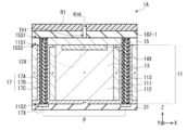
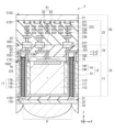
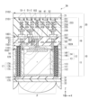
- FIG. 1 is a schematic cross-sectional view showing a configuration example of a lamination cross-section of a photodetector according to a first embodiment of the present disclosure.
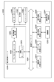
- FIG. 2 is a block diagram showing an example of a schematic configuration of the photodetector shown in FIG.
- FIG. 3A is an example of an equivalent circuit diagram of a unit pixel of the photodetector shown in FIG.
- FIG. 3B is a waveform diagram explaining the operation of the pixel circuit shown in FIG. 3A.
- 4A is a schematic cross-sectional view showing a first structural example of a horizontal cross section of the photodetector shown in FIG. 1.
- FIG. 1 is a schematic cross-sectional view showing a configuration example of a lamination cross-section of a photodetector according to a first embodiment of the present disclosure.
- FIG. 2 is a block diagram showing an example of a schematic configuration of the photodetector shown in FIG.
- FIG. 3A is an example of an
- FIG. 4B is a schematic cross-sectional view showing a second configuration example of the horizontal cross section of the photodetector shown in FIG. 1.
- FIG. 4C is a schematic cross-sectional view showing a third configuration example of the horizontal cross section of the photodetector shown in FIG. 1.
- FIG. 4D is a schematic cross-sectional view showing a fourth configuration example of the horizontal cross section of the photodetector shown in FIG. 1.
- FIG. 4E is a schematic cross-sectional view showing a fifth configuration example of the horizontal cross section of the photodetector shown in FIG. 1.
- FIG. 4F is a schematic cross-sectional view showing a sixth configuration example of the horizontal cross section of the photodetector shown in FIG. 1.
- FIG. 4G is a schematic cross-sectional view showing a seventh structural example of the horizontal cross section of the photodetector shown in FIG. 1.
- FIG. 4H is a schematic cross-sectional view showing an eighth configuration example of the horizontal cross section of the photodetector shown in FIG. 1.
- FIG. FIG. 5 is a schematic cross-sectional view showing a configuration example of a lamination cross-section of the photodetector according to the first modification of the first embodiment.
- 6A is a schematic cross-sectional view showing a first structural example of a horizontal cross section of the photodetector shown in FIG. 5.
- FIG. 6B is a schematic cross-sectional view showing a second configuration example of the horizontal cross section of the photodetector shown in FIG. 5.
- FIG. 5 is a schematic cross-sectional view showing a configuration example of the horizontal cross section of the photodetector shown in FIG. 5.
- FIG. 6C is a schematic cross-sectional view showing a third configuration example of the horizontal cross section of the photodetector shown in FIG. 5.
- FIG. FIG. 7A is a schematic cross-sectional view showing a configuration example of a lamination cross-section of a photodetector according to a second modification of the first embodiment
- FIG. 7B is a schematic cross-sectional view showing a configuration example of a horizontal cross section of the photodetector shown in FIG. 7A
- 8A is a schematic cross-sectional view of lamination representing one step of the method for manufacturing the photodetector shown in FIG. 5.
- FIG. FIG. 8B is a schematic diagram of a lamination cross section showing one step following FIG. 8A.
- FIG. 8C is a schematic diagram of a lamination cross section showing one step following FIG. 8B.
- FIG. 8D is a schematic diagram of a lamination cross section showing one step following FIG. 8C.
- FIG. 8E is a schematic diagram of a lamination cross section showing one step following FIG. 8D.
- FIG. 8F is a schematic diagram of a lamination cross section showing one step following FIG. 8E.
- FIG. 8G is a schematic diagram of a lamination cross section showing one step following FIG. 8F.
- FIG. 8H is a schematic diagram of a lamination cross section showing one step following FIG. 8G.
- FIG. 8I is a schematic diagram of a lamination cross section showing one step following FIG. 8H.
- FIG. 8J is a schematic diagram of a lamination cross section showing one step following FIG. 8I.
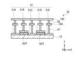
- FIG. 9 is a schematic cross-sectional view showing a configuration example of a lamination cross-section of the photodetector according to the second embodiment of the present disclosure.
- 10A is a schematic cross-sectional view showing one structural example of a horizontal cross section of the photodetector shown in FIG. 9.
- FIG. 10B is a schematic cross-sectional view showing one configuration example of a horizontal cross section of the photodetector shown in FIG. 9.
- FIG. 11 is a schematic cross-sectional view showing a configuration example of a lamination cross-section of a photodetector according to the first modification of the second embodiment.
- FIG. 12 is a schematic cross-sectional view showing a configuration example of a lamination cross-section of a photodetector according to a second modification of the second embodiment.
- 13A is a schematic cross-sectional view showing a configuration example of a lamination cross-section of a photodetector according to a third modification of the second embodiment;
- FIG. 13B is a schematic diagram showing a planar configuration example (planar layout) of the photodetector shown in FIG. 13A.
- 14A is a schematic cross-sectional view showing a configuration example of a lamination cross-section of a photodetector according to a fourth modification of the second embodiment;
- FIG. 14B is a schematic diagram illustrating a planar configuration example (planar layout) of the photodetector illustrated in FIG. 14A.
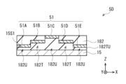
- FIG. 15 is a schematic cross-sectional view showing a configuration example of a lamination cross-section of the photodetector according to the third embodiment of the present disclosure.
- 16A is a schematic cross-sectional view showing a first structural example of a horizontal cross section of the photodetector shown in FIG. 15.
- FIG. 16B is a schematic cross-sectional view showing a second configuration example of the horizontal cross section of the photodetector shown in FIG. 15.
- FIG. FIG. 17 is a schematic cross-sectional view showing a configuration example of a lamination cross-section of the photodetector according to the first modification of the third embodiment.
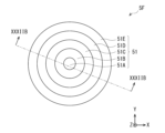
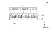
- FIG. 18 is a schematic cross-sectional view showing a configuration example of a lamination cross-section of the photodetector according to the fourth embodiment of the present disclosure.
- 19A is a schematic diagram showing a first structural example of a planar structural example (planar layout) of the photodetector shown in FIG. 18.
- FIG. 19B is a schematic diagram illustrating a second configuration example of the planar configuration example (planar layout) of the photodetector illustrated in FIG. 18.
- FIG. FIG. 20 is an example of an equivalent circuit diagram of a unit pixel of the photodetector shown in FIG. FIG.
- 21A is a schematic diagram illustrating a configuration example of a planar configuration example (planar layout) of a photodetector according to the first modification of the fourth embodiment
- FIG. 21B is a schematic diagram showing a configuration example of a planar configuration example (planar layout) of the photodetector according to the second modification of the fourth embodiment
- 21C is a schematic diagram illustrating a configuration example of a planar configuration example (planar layout) of the photodetector according to the third modification of the fourth embodiment
- FIG. FIG. 22 is a schematic cross-sectional view showing a configuration example of a lamination cross-section of the photodetector according to the fifth embodiment of the present disclosure.
- FIG. 23 is an enlarged cross-sectional view showing an enlarged part of the photodetector shown in FIG. 22.
- FIG. FIG. 24 is a schematic diagram showing a configuration example of a planar configuration example (planar layout) of the photodetector shown in FIG. 25A is a schematic cross-sectional view of a lamination showing one step of the method for manufacturing the photodetector shown in FIG. 22.
- FIG. FIG. 25B is a schematic diagram of a lamination cross section showing one step following FIG. 25A.
- FIG. 25C is a schematic diagram of a lamination cross section showing one step following FIG. 25B.
- FIG. 25D is a schematic diagram of a lamination cross section showing one step following FIG. 25C.
- FIG. 25E is a schematic diagram of a lamination cross section showing one step following FIG. 25D.
- FIG. 25F is a schematic diagram of a lamination cross section showing one step following FIG. 25E.
- FIG. 25G is a schematic diagram of a lamination cross section showing one step following FIG. 25F.
- FIG. 25H is a schematic diagram of a lamination cross section showing one step following FIG. 25G.
- FIG. 25I is a schematic diagram of a lamination cross section showing one step following FIG. 25H.
- FIG. 26 is an enlarged cross-sectional view showing an enlarged part of the photodetector according to the first modification of the fifth embodiment of the present disclosure.
- FIG. 27A is a schematic cross-sectional view of a lamination showing one step of the method for manufacturing the photodetector shown in FIG. 26.
- FIG. FIG. 27B is a schematic diagram of a lamination cross section showing one step following FIG. 27A.
- FIG. 27C is a schematic diagram of a lamination cross section showing one step following FIG. 27B.
- FIG. 27D is a schematic diagram of a lamination cross section showing one step following FIG. 27C.
- FIG. 27E is a schematic diagram of a lamination cross section showing one step following FIG. 27D.
- FIG. 27F is a schematic diagram of a lamination cross section showing one step following FIG. 27E.
- FIG. 28 is an enlarged cross-sectional view showing an enlarged part of the photodetector according to the second modification of the fifth embodiment of the present disclosure.
- FIG. 29 is an enlarged cross-sectional view showing an enlarged part of the photodetector according to the third modification of the fifth embodiment of the present disclosure.
- FIG. 30 is an enlarged cross-sectional view showing an enlarged part of the photodetector according to the fourth modification of the fifth embodiment of the present disclosure.
- FIG. 31 is an enlarged cross-sectional view showing an enlarged part of the photodetector according to the fifth modification of the fifth embodiment of the present disclosure.
- FIG. 32A is an enlarged plan view showing an enlarged part of the photodetector according to the sixth modification of the fifth embodiment of the present disclosure.
- FIG. 32B is an enlarged cross-sectional view showing an enlarged part of the photodetector shown in FIG. 32A.
- FIG. 33 is an enlarged plan view showing an enlarged part of the photodetector according to the seventh modification of the fifth embodiment of the present disclosure.
- FIG. 34 is a functional block diagram showing an example of an electronic device using the photodetector shown in FIG. 1 and the like.
- FIG. 35 is a block diagram showing an example of a schematic configuration of a vehicle control system.
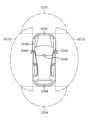
- FIG. 36 is an explanatory diagram showing an example of installation positions of the vehicle exterior information detection unit and the imaging unit.
- the above patent document discloses a structure in which a quench resistor is connected to the cathode via a metal electrode.
- the high-concentration layer is formed by, for example, ion implantation.
- ion implantation may cause crystal defects.
- the Si substrate may be damaged during the formation of the metal electrodes. Such a possibility is a factor in reducing the reliability of APDs.
- the graphene layer constitutes the quench resistor in the above patent document, a certain length is required in order to secure a sufficient resistance value as the quench resistor, which may hinder miniaturization. Therefore, the applicant of the present application has come to provide a highly reliable photodetector that is compatible with miniaturization.
- FIG. 1 schematically illustrates an example of a cross-sectional configuration of a photodetector 1 according to the first embodiment of the present disclosure.
- FIG. 2 is a block diagram showing a schematic configuration of the photodetector 1 shown in FIG. 3A is a circuit diagram showing an example of an equivalent circuit of the unit pixel P of the photodetector 1 shown in FIG. 1.
- FIG. The photodetector 1 can be applied to, for example, a distance image sensor (distance image apparatus 1000 described later, see FIG. 34), an image sensor, or the like that measures distance by the ToF (Time-of-Flight) method.
- a distance image sensor distance image apparatus 1000 described later, see FIG. 34
- ToF Time-of-Flight
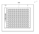
- the photodetector 1 has, for example, a pixel array section 100A in which a plurality of unit pixels P are arranged in an array in row and column directions.
- the photodetector 1 has a pixel array section 100A and a bias voltage application section 110, as shown in FIG.
- the bias voltage applying section 110 applies a bias voltage to each unit pixel P of the pixel array section 100A.
- a case of reading electrons as signal charges will be described.
- the unit pixel P includes a light receiving element 12, a clamp circuit 50 as a protection circuit, a first control transistor 71, a current source 72, a terminal 73, and a second control transistor 74. , and a readout circuit 75 .
- the light receiving element 12 converts incident light into an electric signal by photoelectric conversion and outputs the electric signal. Additionally, the light-receiving element 12 converts incident light (photons) into an electrical signal by photoelectric conversion, and outputs a pulse corresponding to the incidence of the photons.
- the light receiving element 12 is, for example, a SPAD element.
- the SPAD element forms an avalanche multiplication region (depletion layer) 12X, for example, by applying a large negative voltage to the cathode, and generates light in response to the incidence of one photon. It has the characteristic that electrons cause avalanche multiplication and a large current flows.
- the anode of the light receiving element 12 is connected, for example, to the bias voltage applying section 110 .
- the cathode of the light receiving element 12 is connected to a terminal 73 to which a power supply voltage VDD is applied via, for example, a first control transistor 71 and a current source 72 .
- a power supply voltage VDD for example, a voltage of about 3V is applied.
- a cathode of the light receiving element 12 is connected to a source terminal of the first control transistor 71 .
- a device voltage VB is applied to the anode of the light receiving element 12 from a device voltage applying section.
- the device voltage VB a large negative voltage at which avalanche multiplication occurs, that is, a voltage higher than the breakdown voltage (for example, about -20 V) is applied.
- the first control transistor 71 is composed of a p-type MOSFET (Metal-Oxide-Semiconductor Field-Effect Transistor) and is also called a quenching resistance element.
- the first control transistor 71 is connected in series with the light receiving element 12 via the clamp circuit 50 .
- the source terminal of the first control transistor 71 is connected to the cathode of the light receiving element 12 and the drain terminal of the first control transistor 71 is connected to the terminal 73 via the current source 72 .
- the first control transistor 71 becomes conductive when the enable signal EN applied to the gate electrode becomes low level, and the current from the current source 72 flows to the light receiving element 12 .
- the second control transistor 74 is connected between the cathode of the light receiving element 12 and a reference potential node (eg, ground).
- the second control transistor 74 is, for example, an N-type MOS transistor.
- the second control transistor 74 becomes conductive when the signal xEN opposite in phase to the enable signal EN is applied to the gate electrode, and makes the voltage applied to the light receiving element 12 equal to or lower than the breakdown voltage. It is designed to be in an activated state.
- the readout circuit 75 is, for example, a CMOS inverter circuit including a P-type MOS transistor Qp and an N-type MOS transistor Qn.
- the readout circuit 75 has an input terminal connected to the cathode of the light receiving element 12, the source terminal of the first control transistor 71, and the second control transistor 74, and an output terminal connected to the arithmetic processing section 76, which will be described later. .
- the readout circuit 75 outputs a received light signal based on the carrier (signal charge) multiplied by the light receiving element 12 . More specifically, the readout circuit 75 shapes the voltage generated by the electrons multiplied by the light receiving element 12 .
- the readout circuit 75 outputs, to the arithmetic processing section 76, a light reception signal, for example, a pulse waveform generated from the arrival time of one photon.
- a light reception signal for example, a pulse waveform generated from the arrival time of one photon.
- the arithmetic processing unit 76 calculates the distance for each unit pixel P by performing arithmetic processing to obtain the distance to the object based on the timing at which a pulse indicating the arrival time of one photon is generated in each light reception signal. Based on these distances, a distance image is generated in which the distances to the subject detected by the plurality of unit pixels P are arranged two-dimensionally.
- the clamp circuit 50 is a protection circuit provided between the light receiving element 12 and the input end of the readout circuit 75 .
- the clamp circuit 50 suppresses the P-type MOS transistor Qp and the N-type MOS transistor Qn constituting the readout circuit 75 and the first control transistor from an overvoltage generated when the light receiving element 12 is irradiated with a large amount of laser light, for example.
- 71 and the second control transistor 74 are overvoltage protection circuits.
- the clamp circuit 50 between the light receiving element 12 and the input terminal of the readout circuit 75, even if the light receiving element 12 is irradiated with a large amount of laser light exceeding a predetermined light amount (more than expected), Even if there is, the read circuit 75 and the like can be protected from overvoltage.
- the clamp circuit 50 has, for example, a resistive element 51, a first clamp element 54, and a second clamp element 55, as specifically shown in FIG.
- One end of the resistance element 51 is connected to the cathode electrode of the light receiving element 12 .
- the first clamp element 54 is, for example, a clamp diode having a cathode connected to the other end (output end) of the resistance element 51 and an anode connected to a reference potential node (eg, ground).
- the resistance element 51 is provided to limit the current value flowing through the first clamping element 54 so as not to exceed its rated forward current when overvoltage occurs in the light receiving element 12 .
- the clamp diode which is the first clamp element 54, clamps the overvoltage to a constant voltage (forward voltage VF) when an overvoltage exceeding the clamp voltage occurs in the light receiving element 12.
- first clamping element 54 is not limited to a clamping diode.
- a Schottky barrier diode or the like can be used as the first clamping element 54 in addition to the clamping diode.
- the second clamp element 55 is composed of, for example, a P-type MOS transistor.
- the second clamping element 55 is connected between the first clamping element 72 (for example, the anode of the clamping diode) and a node N to which the input terminal of the readout circuit 75 is connected.
- a P-type MOS transistor as the second clamp element 55 has a gate electrode connected to a reference potential node (for example, ground) and a back gate connected to a source electrode.
- the clamping operation when an overvoltage of minus several tens of volts is generated in the light receiving element 12 will be described with reference to the waveform diagram of FIG. 3B.
- the clamp diode as the first clamp element 54 clamps the overvoltage generated in the light receiving element 12 to a constant voltage (forward voltage VF). Due to this clamping operation, the overvoltage generated in the light receiving element 12 is clamped to a negative voltage of about -1V to -3V, for example.
- the negative voltage when a negative voltage is generated by the clamping operation of the first clamping element 54, the negative voltage may exceed the withstand voltage of the MOS transistor, which will be described later.
- a second clamping device 55 is provided to address this negative voltage problem. That is, the second clamp element 55 clamps the voltage of the node N to which the input terminal of the readout circuit 75 is connected to the gate-source voltage Vgs (for example, about 0.5 V) of the P-type MOS transistor. As a result, the clamping operation of the first clamping element 54 can solve the negative voltage problem.
- the photodetector 1 is a so-called back-illuminated photodetector.
- the photodetector 1 includes, for example, a logic substrate 20 laminated on a surface of a sensor substrate 10 (for example, a first surface 11S1 which is a surface of a semiconductor substrate 11 constituting the sensor substrate 10). Light is received from the rear surface of the sensor substrate 10 (the second surface 11S2, which is the rear surface of the semiconductor substrate 11 forming the sensor substrate 10).
- the photodetector 1 has a light receiving element 12 for each unit pixel P. As shown in FIG.
- the light-receiving element 12 has a light-receiving portion 13 and a multiplier portion 14 , and the light-receiving portion 13 is embedded in the semiconductor substrate 11 .
- Semiconductor substrate 11 further includes p-type semiconductor region (p+) 14X among p-type semiconductor region (p+) 14X and n-type semiconductor region (n+) 14Y forming multiplier section 14 on first surface 11S1. It is A semiconductor layer 15 is provided on the first surface 11S1 side of the semiconductor substrate 11 .
- the semiconductor layer 15 is provided with an n-type semiconductor region (n+) 14 ⁇ /b>Y forming the multiplier section 14 .
- the sensor substrate 10 has, for example, a semiconductor substrate 11 made of a silicon substrate, a semiconductor layer 15, and a multilayer wiring layer 18.
- the semiconductor substrate 11 has a first surface 11S1 and a second surface 11S2 facing each other.
- the semiconductor substrate 11 has a p-well (p) 111 common to a plurality of unit pixels P.
- the semiconductor substrate 11 is provided with an n-type semiconductor region (n) 112 whose impurity concentration is controlled to be n-type, for example, for each unit pixel P, thereby forming a light receiving element 12 for each unit pixel P.
- n semiconductor region
- the semiconductor substrate 11 is further provided with a pixel separation portion 17 extending from the first surface 1S1 to the second surface 11S2.
- the light receiving element 12 has a multiplication region for avalanche multiplication of carriers by a high electric field region, that is, an avalanche multiplication region.
- the light receiving element 12 is a SPAD capable of forming an avalanche multiplication region (depletion layer) by applying a large positive voltage to the cathode and avalanche-multiplying electrons generated by the incidence of one photon. element.
- the light receiving element 12 has a light receiving section 13 and a multiplier section 14 .
- the light receiving section 13 performs photoelectric conversion by absorbing light incident from the second surface 11S2 side of the semiconductor substrate 11 and generating carriers according to the amount of received light.
- the light receiving portion 13 includes the n-type semiconductor region (n) 112 whose impurity concentration is controlled to be n-type, as described above. Carriers (electrons) generated in the light receiving section 13 are transferred to the multiplication section 14 due to the potential gradient. Note that the light receiving unit 13 is a specific example corresponding to the “light receiving unit” of the present disclosure.
- the multiplication unit 14 avalanche-multiplies the carriers (here, electrons) generated in the light receiving unit 13 .
- the multiplication unit 14 includes, for example, a p-type semiconductor region (p+) 14X having a higher impurity concentration than the p-well (p) 111 and an n-type semiconductor region (n+) 14X having a higher impurity concentration than the n-type semiconductor region (n) 112. ) 14Y.
- the p-type semiconductor region (p+) 14X is provided in the semiconductor substrate 11 so as to face the first surface 11S1.
- the n-type semiconductor region (n+) 14Y is provided so as to protrude from the first surface 11S1 of the semiconductor substrate 11 .
- the multiplier 14 is a specific example corresponding to the “multiplier” of the present disclosure.
- a p-type semiconductor region (p+) 14X provided facing the first surface 11S1 of the semiconductor substrate 11 and an n-type semiconductor region (p+) provided facing the second surface 15S2 of the semiconductor layer 15
- An avalanche multiplication region 12X is formed at the junction with n+) 14Y.
- the avalanche multiplication region 12X is a high electric field region, ie a depletion layer, formed by a large negative voltage applied to the anode.
- the avalanche multiplication region 12X is formed at the interface between the p-type semiconductor region (p+) 14X and the n-type semiconductor region (n+) 14Y. In the avalanche multiplication region 12X, electrons (e ⁇ ) generated by one photon incident on the light receiving element 12 are multiplied.
- the semiconductor layer 15 is a semiconductor layer made of silicon, for example, formed on the first surface 11S1 of the semiconductor substrate 11 using, for example, an epitaxial crystal growth method, and corresponds to a specific example of the "semiconductor layer" of the present disclosure. It is.
- the semiconductor layer 15 has a first surface 15S1 and a second surface 15S2 facing each other.
- the first surface 15 S 1 faces the multilayer wiring layer 18 and the second surface 15 S 2 faces the semiconductor substrate 11 .
- the semiconductor layer 15 is embedded with the n-type semiconductor region (n+) 14Y facing the second surface 15S2.
- a contact electrode 16 is further provided on the n-type semiconductor region (n+) 14Y so as to face the first surface 15S1.
- the contact electrode 16 is a cathode as a specific example corresponding to the “first electrode” of the present disclosure, and is electrically connected to the multiplier section 14 .
- the contact electrode 16 is composed of, for example, an n-type semiconductor region (n++) having a higher impurity concentration than the n-type semiconductor region (n+) 14Y.
- the pixel separating section 17 electrically separates the adjacent unit pixels P, and is provided in the pixel array section 100A in a grid pattern so as to surround each of the plurality of unit pixels P in plan view, for example. .
- the pixel separating portion 17 extends from the second surface 11S2 of the semiconductor substrate 11 to the first surface 15S1 of the semiconductor layer 15. As shown in FIG. That is, the pixel separating portion 17 penetrates the semiconductor substrate 11 and the semiconductor layer 15 .
- the pixel separation section 17 is formed using insulating films 17B and 17C such as silicon oxide (SiOx) films and a light shielding film 17A.
- a p-type semiconductor region (p+) 113 having a higher impurity concentration than the p-well 111 is provided around the pixel isolation portion 17 .
- the p-type semiconductor region (p+) 113 includes an extension portion 113X extending toward the inside of the unit pixel P in the vicinity of the first surface 11S1 of the semiconductor substrate 11 (see FIG. 1).
- the extended portion 113X is an anode as a specific example corresponding to the “second electrode” of the present disclosure, and also serves as a contact electrode electrically connected to the light receiving portion 13 .
- the p-type semiconductor region (p+) 113 further extends along the second surface 11S2 of the semiconductor substrate 11. As shown in FIG.
- a semiconductor layer 15 and a multilayer wiring layer 18 are laminated in order on the first surface 11S1 of the semiconductor substrate 11 opposite to the second surface 11S2, which is the light incident surface.
- a wiring layer 181 made up of one or more wirings is embedded in an interlayer insulating layer 182 .
- the wiring layer 181 is, for example, a path for supplying a voltage to be applied to the semiconductor substrate 11 and the light receiving element 12 and extracting carriers generated in the light receiving element 12 .
- Some of the wirings in the wiring layer 181 are electrically connected to the contact electrodes 16 and the extended portions 113X through the vias V1.
- a plurality of pad electrodes 183 are embedded in the vicinity of the surface of the interlayer insulating layer 182 opposite to the semiconductor substrate 11 (the surface 18S1 of the multilayer wiring layer 18).
- the plurality of pad electrodes 183 are electrically connected to some wirings of the wiring layer 181 via vias V2.
- FIG. 1 shows an example in which one wiring layer 181 is formed in the multilayer wiring layer 18, the number of layers of the wiring layers 181 embedded in the multilayer wiring layer 18 is not limited.
- a wiring layer may be formed.
- the interlayer insulating layer 182 is, for example, a single layer film made of one of silicon oxide (SiOx), TEOS, silicon nitride (SiNx) and silicon oxynitride (SiOxNy), or made of two or more of these. It is composed of a laminated film.
- the wiring layer 181 is formed using, for example, aluminum (Al), copper (Cu), tungsten (W), or the like.
- the pad electrode 183 is exposed on the surface 18S1 of the multilayer wiring layer 18, which is the bonding surface with the logic substrate 20. As shown in FIG. The pad electrode 183 is used for connection with the logic substrate 20, for example.
- the pad electrode 183 is formed using copper (Cu), for example.
- a resistance element 51 is further provided in the interlayer insulating layer 182 .
- the resistor element 51 is electrically connected to the contact layer 16 and is a resistor made of a polycrystalline semiconductor material such as polysilicon (Poly-Si) containing an n-type impurity element.
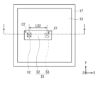
- the resistive element 51 is, for example, the first It has a body portion 52 extending parallel to the surface 11S1, that is, extending along the XY plane, and a lead-out portion 53 connecting the body portion 52 and the contact layer 16 .
- the body portion 52 is formed on the same layer as the wiring layer 181 in the example of the structure shown in FIG. However, the body portion 52 of the resistance element 51 may be provided on a layer different from the wiring layer 181 .
- the distance between the lower surface of the body portion 52 and the upper surface of the contact layer 16, that is, the thickness G1 of the portion of the interlayer insulating layer 182 sandwiched between the body portion 52 and the contact layer 16 (see FIG. 1) is preferably greater than 150 nm when the dielectric constant ⁇ of the material forming the interlayer insulating layer 182 is 4.2. If the thickness G1 is smaller than this, a strong electric field is generated at an unintended location between the main body portion 52 and the multiplier portion 14, that is, at a location other than the first connection portion C1, and unintended avalanche multiplication of electrons occurs. This is because it may occur.
- a via V2 is provided upright on the upper surface of the main body portion 52 .
- the resistance element 51 is electrically connected to the pad electrode 183 through the via V2.
- another wiring layer such as the wiring layer 181 may be further provided between the body portion 52 and the via V2, for example.
- the via V2 connected to the resistance element 51 is a specific example corresponding to the "first wiring" of the present disclosure.
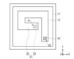
- the position in the XY plane of the first connection portion C1 between the extraction portion 53 of the resistance element 51 and the contact layer 16 and the main body portion 52 of the resistance element 51 and the positions of the second connecting portion C2 with the via V2 in the XY plane are preferably different from each other in the XY plane. That is, it is preferable that the lead-out portion 53 and the via V2 are arranged so as not to overlap each other in the stacking direction (Z-axis direction) orthogonal to the first surface 11S1. This is because the resistance value of the resistance element 51, that is, the resistance value between the contact layer 16 and the via V2 increases in proportion to the path length L52.
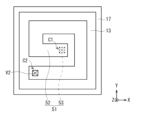
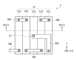
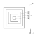
- 4A is a schematic cross-sectional view showing a first configuration example (planar layout) of the XY cross section of the photodetector 1.
- the first connection portion C1 is located, for example, in the central region of the pixel P in the XY plane, and the second connection portion C2 is located in the peripheral region of the pixel P in the XY plane. do.
- the main body portion 52 extends linearly in the XY plane, but the present disclosure is not limited to this.
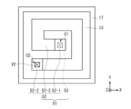
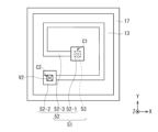
- the body portion 52 includes one bent portion on the path from the first connection portion C1 to the second connection portion C2.
- the body portion 52 includes two bent portions on the route from the first connection portion C1 to the second connection portion C2.
- the body portion 52 includes three bent portions on the route from the first connection portion C1 to the second connection portion C2. Furthermore, in the fifth configuration example of FIG. 4E, the body portion 52 spirally extends from the central region of the pixel P toward the peripheral region of the pixel P in the XY plane. In FIG. 4E, the body portion 52 has a shape that makes only about one turn, but in the present disclosure, the body portion 52 may have a spiral shape that makes multiple turns.
- 4B to 4E are schematic cross-sectional views showing second to fifth configuration examples of the XY cross section of the photodetector 1. FIG.
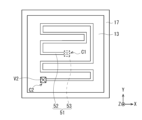
- the shape of the body portion 52 in the XY plane is not limited to being spiral, and may include a serpentine portion, as shown in FIG. 4F, for example.
- the width of the body portion 52 may be smaller than the dimensions of the lead-out portion 53 in the XY plane and the dimensions of the via V2 in the XY plane.
- FIG. 4F is a schematic cross-sectional view showing a sixth configuration example of the XY cross section of the photodetector 1 .
- the first portion 52-1 is a portion of the body portion 52 that is connected to the extraction portion 53
- the second portion 52-2 is a portion of the body portion 52 that is connected to the via V2
- 52-3 is a central portion in the longitudinal direction connecting the first portion 52-1 and the second portion 52-2 of the body portion 52.
- the third portion 52-3 has the highest volume resistivity, and the first portion 52-1 and the second portion 52-2 are lower than the third portion 52-3. It is preferable to have volume resistivity.
- the third portion 52-3 may be made to have a high resistance.
- the third portion 52-3 may be made to have a high resistance.
- the resistance of the third portion 52-3 may be increased by adding at least one of O (oxygen) and N (nitrogen) to the third portion 52-3 and performing heat treatment.
- Si silicon
- Ar argon
- the resistance of the third portion 52-3 is increased. You may do so.
- the width of the third portion 52-3 of the main body portion 52 is set to the width of the first portion 52-1, for example, as in the eighth configuration example of the XY cross section of the photodetector 1 shown in FIG. 4H. and the width of the second portion 52-2 to increase the resistance of the third portion 52-3.
- the logic board 20 has, for example, a semiconductor substrate 21 made of a silicon substrate and a multilayer wiring layer 22 .
- the logic board 20 includes, for example, the bias voltage application section 110 described above, a readout circuit for outputting pixel signals based on charges output from the unit pixels P of the pixel array section 100A, a vertical drive circuit, a horizontal drive circuit, and an output circuit.
- a logic circuit including circuits and the like is configured. Note that the logic circuit may include a column signal processing circuit.
- a gate wiring 221 of a transistor constituting a readout circuit and wiring layers 222, 223, 224, 225 including one or more wirings are stacked in order from the semiconductor substrate 21 side.
- An interlayer insulating layer 226 is provided in the gap between the gate wiring 221 of the transistor and the wiring layers 222, 223, 224, 225 including one or more wirings.
- a plurality of pad electrodes 227 are embedded in a surface 22S1 of the multilayer wiring layer 22, which is the surface of the interlayer insulating layer 226 opposite to the semiconductor substrate 21. As shown in FIG. The plurality of pad electrodes 227 are electrically connected to some wirings of the wiring layer 225 via vias V3.
- the interlayer insulating layer 117 is, for example, a single-layer film made of one of silicon oxide (SiOx), TEOS, silicon nitride (SiNx), silicon oxynitride (SiOxNy), or the like. It is composed of a laminated film composed of two or more kinds of single-layer films.
- the gate wiring 221 and the wiring layers 222, 223, 224, and 225 are formed using, for example, aluminum (Al), copper (Cu), or tungsten (W), like the wiring layer 181.
- the pad electrodes 227 are exposed on the surface 22S1 of the multilayer wiring layer 22, which is the joint surface with the sensor substrate 10, and are connected to the pad electrodes 183 of the sensor substrate 10, for example.
- the pad electrode 227 is formed using copper (Cu), for example, like the pad electrode 183 .
- the pad electrode 183 and the pad electrode 227 are, for example, CuCu bonded.
- the cathode of the light receiving element 12 is electrically connected to the quenching resistance element 120 provided on the logic substrate 20 side, and the anode of the light receiving element 12 is electrically connected to the bias voltage applying section 110 .
- a microlens 33 is provided for each unit pixel P, for example, via a passivation film 31 and a color filter 32, for example.
- the microlens 33 converges the light incident from above onto the light receiving element 12, and is made of, for example, silicon oxide (SiOx).
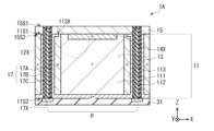
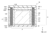
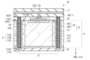
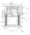
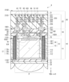
- FIG. 5 schematically illustrates an example of a layered cross-sectional configuration of a photodetector 1A as a first modified example according to the first embodiment of the present disclosure.
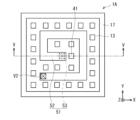
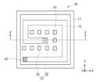
- 6A to 6C are schematic cross-sectional views showing first to third configuration examples (planar layout) of the XY cross section of the photodetector 1A shown in FIG. 5, respectively.
- the photodetector 1A further includes a reflective layer 41 as shown in FIGS. 5 and 6A to 6C.
- the configuration of the photodetector 1A is substantially the same as the configuration of the photodetector 1, except that the reflective layer 41 is further provided.
- a plurality of reflective layers 41 are discretely arranged along the XY plane around the body portion 52 , for example, on the same layer as the body portion 52 .
- the reflective layer 41 can be formed using, for example, a wiring material having light reflectivity such as aluminum (Al).
- the reflective layer 41 can also be formed using a nonmetallic material such as silicon oxide.
- the reflective layer 41 may be made of the same kind of material as the polycrystalline semiconductor material forming the body portion 52 .
- the reflective layer 41 is provided in the photodetector 1A of this modified example.
- the light transmitted through the light receiving section 13 without being absorbed is reflected by the reflective layer 41 and enters the light receiving section 13 again. Therefore, compared with the photodetector 1 that does not have the reflective layer 41, it is possible to further improve the sensitivity to incident light.
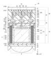
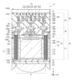
- FIG. 7A schematically illustrates an example of a laminated cross-sectional configuration of a photodetector 1B as a second modified example according to the first embodiment of the present disclosure.
- FIG. 7B is a schematic cross-sectional view showing a configuration example (planar layout) of the XY cross section of the photodetector 1B shown in FIG. 7A.
- the photodetector 1B like the photodetector 1A, further includes a plurality of reflective layers 41 as shown in FIGS. 7A and 7B.
- a plurality of reflective layers 41 are discretely arranged along the XY plane.
- the photodetector 1B further includes a plurality of reflective layers 41 in the layer between the layer on which the body portion 52 is provided and the layer on which the contact layer 16 is provided.
- the body portion 52 and one reflective layer 41C of the plurality of reflective layers 41 overlap in the thickness direction (Z-axis direction).
- the reflective layer 41 ⁇ /b>C may electrically connect the body portion 52 and the contact layer 16 .
- the reflective layer 41C is connected to the body portion 52 through the extraction portion 53, and is connected to the contact layer 16 through the via V2.
- the reflective layer 41 can be formed using, for example, a wiring material having light reflectivity such as aluminum (Al).
- the reflective layer 41 can also be formed using a nonmetallic material such as silicon oxide.
- the reflective layer 41 may be made of the same kind of polycrystalline semiconductor material as the polycrystalline semiconductor material forming the body portion 52, or may be made of a polycrystalline semiconductor material different in kind from the polycrystalline semiconductor material forming the body portion 52. It may be configured by
- FIGS. 8A to 8J are schematic cross-sectional views of laminated layers representing one step of the method for manufacturing the photodetector 1A.
- a semiconductor substrate 11 is prepared.
- a p-well (p) 111, an n-type semiconductor region (n) 112, a p-type semiconductor region (p+) 113 and p-type semiconductor regions (p+) 113 are formed in the semiconductor substrate 11 by controlling the concentration of p-type or n-type impurities.
- type semiconductor regions (p+) 14X are respectively formed.
- a semiconductor layer 15 made of, for example, silicon (Si) is formed on the first surface 11S1 of the semiconductor substrate 11 by an epitaxial crystal growth method such as a metal organic chemical vapor deposition (MOCVD) method. do.
- MOCVD metal organic chemical vapor deposition
- the semiconductor layer 15 and the semiconductor substrate are etched by etching. 11 is formed through a through hole.
- the insulating films 17B and 17C and the light shielding film 17A are sequentially formed inside the through holes by, for example, a CVD (Chemical Vapor Deposition) method, a PVD (Physical Vapor Deposition) method, an ALD (Atomic Layer Deposition) method, or a vapor deposition method. film.
- CVD Chemical Vapor Deposition
- PVD Physical Vapor Deposition
- ALD Atomic Layer Deposition
- an interlayer insulating layer 182-1 is formed on the first surface 15S1 of the semiconductor layer 15, as shown in FIG. 8B.
- the first surface 15S1 of the semiconductor layer 15 may be planarized by, for example, CMP (Chemical Mechanical Polishing) before forming the interlayer insulating layer 182-1.
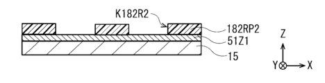
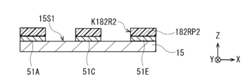
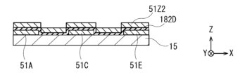
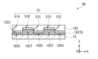
- a resist mask R1 including an opening R1K is formed on the interlayer insulating layer 182-1 by photolithography. Further, a through hole TH1 is formed in the interlayer insulating layer 182-1 by dry etching such as RIE using the resist mask R1 or wet etching. The through hole TH1 is formed at a position overlapping the p-type semiconductor region (p+) 14X near the center of the light receiving portion 13. As shown in FIG. After forming the through hole TH1, the resist mask R1 is removed.
- a polycrystalline semiconductor material such as polysilicon doped with an n-type impurity element such as P (phosphorus) or As (arsenic) is deposited so as to cover the interlayer insulating layer 182-1. is used to form a polycrystalline semiconductor layer 52Z.
- a film of pure polysilicon containing no n-type impurities may be formed, and then n-type impurities may be ion-implanted.
- the contact layer 16 and the n-type semiconductor region (n+) 14Y are formed in a self-aligned manner by diffusing the n-type impurity from the lead-out portion 53. Therefore, compared with the case of forming by ion implantation, for example, Thus, the contact layer 16 and the n-type semiconductor region (n+) 14Y can be formed in a narrower region with high precision.
- the insulating film Z is removed.
- a photolithographic method is used on the polycrystalline semiconductor layer 52Z to form a resist mask R2 including an opening R2K at a predetermined position.
- the semiconductor layer 52Z is selectively removed by RIE or the like.
- the body portion 52 and the reflective layer 41 are formed at predetermined positions on the interlayer insulating layer 182-1.
- the resistive element 51 composed of the extraction portion 53 and the main body portion 52 is obtained.
- an interlayer insulating layer 182-2 is formed so as to cover the interlayer insulating layer 182-1, the main body portion 52, and the reflective layer 41.
- the upper surface of the interlayer insulating layer 182-2 is planarized in accordance with the above.
- an interlayer insulating layer 182 consisting of an interlayer insulating layer 182-1 and an interlayer insulating layer 182-2 is obtained.
- a portion of the interlayer insulating layer 182 and a portion of the semiconductor layer 15 are selectively removed using, for example, photolithography, and a position corresponding to the extended portion 113X in the Z-axis direction is removed.
- the via V1 is formed by filling the opening with a conductive metal material such as W (tungsten).
- W tungsten
- the interlayer insulating layer 182 around the via V1 is selectively removed to form the wiring layer 181 on the via V1.
- through holes TH2 are formed in the interlayer insulating layer 182.
- the through holes TH2 are formed at a position corresponding to the wiring layer 181 and at a position corresponding to the main body portion 52 .
- vias V2 are formed by filling the through holes TH2 with a conductive metal material such as W (tungsten).
- pad electrodes 183 are formed so as to be in contact with the upper surfaces of the vias V2, and the periphery of the pad electrodes 183 is filled with an interlayer insulating layer 182. Then, as shown in FIG. Furthermore, by flattening the upper surfaces of the pad electrodes 183 and the interlayer insulating layer 182, the multilayer wiring layer 18 having a flat surface 18S1 is obtained. Thereby, the sensor substrate 10 is completed.
- the separately produced logic board 20 is attached to the sensor board 10 .
- a plurality of pad electrodes 183 exposed on the surface 18S1 of the multilayer wiring layer 18 serving as the bonding surface of the sensor substrate 10 and a plurality of pad portions exposed on the surface 22S of the multilayer wiring layer 22 serving as the bonding surface of the logic substrate 20 are formed.
- 217 are Cu—Cu bonded.
- the photodetector 1A shown in FIG. 5 is completed.
- the photodetector 1 of the present embodiment the photodetector 1A as the first modified example, and the photodetector 1B as the second modified example (hereinafter referred to as the photodetector 1 of the present embodiment, etc.) 1
- a resistance element 51 made of a polycrystalline semiconductor material is connected to the contact layer 16 electrically connected to the multiplier section 14 .
- the semiconductor substrate 11 such as a Si substrate does not come into direct contact with the metal, a silicidation reaction between Si and the metal element does not occur, and the metal element can be prevented from entering the semiconductor substrate 11 . can. Therefore, the structural stability of the semiconductor substrate 11 is enhanced as compared with the case where the resistance element 51 is made of metal. That is, since it is possible to suppress the occurrence of crystal structure defects in the semiconductor substrate 11, it is possible to obtain high operational reliability of the semiconductor substrate 11, such as ensuring a sufficient withstand voltage.
- the resistance element 51 has a body portion 52 extending in the XY plane, and a take-out portion 53 extending in the stacking direction (Z-axis direction) so as to connect the contact layer 16 and the body portion 52 . Therefore, the resistance value of the resistance element 51 can be arbitrarily set by forming the body portion 52 in a linear shape and adjusting the length of the path.
- the resistance element 51 is made of a polycrystalline semiconductor such as polysilicon, it is easier to achieve a higher resistance than when the resistance element 51 is made of a metal material, and an unintended parasitic capacitance is also reduced. can be reduced. Furthermore, it is possible to reduce the power consumption required during operation, and it is also advantageous for speeding up.
- the diffusion layer such as the contact layer 16 is manufactured in a self-aligned manner by diffusing the n-type impurity contained in the lead-out portion 53 of the resistance element 51. It is possible. Therefore, it is not necessary to implant ions into the semiconductor substrate 11 to form a diffusion layer, and the crystal structure of the semiconductor substrate 11 can be stably maintained.
- the resistance element 51 constitutes a clamp circuit 50 as a protection circuit. Therefore, it is possible to avoid damage to the readout circuit 75 and the like due to an overvoltage that occurs when the light receiving element 12 is irradiated with a large amount of laser light, for example.
- the photodetection devices 1A and 1B since a plurality of reflection layers 41 are provided, the light that has been incident from the second surface 11S2 and has passed through the light receiving section 13 is reflected and made to enter the light receiving section 13 again. can be done. Therefore, higher photodetection sensitivity can be obtained.
- a single photon avalanche diode (SPAD) element for example, is known as a light receiving element that generates a signal in response to receiving a photon.
- SPAD single photon avalanche diode
- a voltage higher than the breakdown voltage is applied to the anode electrode (or cathode electrode) of the SPAD element to use the SPAD element ( For example, see JP-A-2019-125717).
- the SPAD element when the SPAD element is irradiated with a large amount of laser light more than expected (a predetermined amount of light or more), such as when the SPAD element is directly irradiated with the laser beam, the SPAD element cannot perform photoelectric conversion with the large amount of light. As the influence becomes stronger, the internal impedance drops significantly. As a result, an excessive voltage is applied to the readout circuit that reads out the signal generated by the SPAD element, and the circuit elements constituting the readout circuit may be damaged. Therefore, in order to protect the readout circuit, a configuration has been proposed in which a resistive element made of metal is directly connected to the SPAD element (for example, Japanese Patent Application Laid-Open No. 2020-153929). Recently, however, there has been an increasing demand for further miniaturization of such light receiving elements and photodetectors equipped with such light receiving elements. Under these circumstances, the applicant of the present application has come to provide a highly reliable photodetector that can be miniaturized.
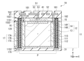
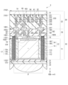
- FIG. 9 schematically illustrates an example of a cross-sectional configuration of the photodetector 2 according to the second embodiment of the present disclosure.
- FIGS. 10A and 10B are schematic cross-sectional views showing one structural example of the horizontal cross section of the photodetector 2 shown in FIG. 9, respectively.
- FIG. 10A represents a horizontal cross section at the height position Lv1 shown in FIG. 9, and
- FIG. 10B represents a horizontal cross section at the height position Lv2 shown in FIG.
- FIG. 9 shows a cross section in the arrow direction along the IX-IX section line shown in FIGS. 10A and 10B.
- the same reference numerals are given to the same components as those of the photodetector 1 of the first embodiment, and the description thereof will be omitted as appropriate.
- the via V1 electrically connected to the p-type semiconductor region (p+) 113 as an anode corresponds to the light receiving section 13 of each pixel P in the cross section parallel to the XY plane. It is provided so as to surround the area where the Also, the vias V1 surrounding the light receiving portions 13 of the adjacent pixels P are provided so as to be connected to each other. Therefore, contact resistance on the anode side can be reduced.
- the pixel separation section 17 is provided inside the semiconductor substrate 11 so as to surround the light receiving section 13 in a cross section parallel to the XY plane, and separates the plurality of pixels P from each other.
- the wiring layer 181 is provided so as to form a lattice shape in a cross section parallel to the XY plane so as to overlap the pixel separating portion 17 in the thickness direction (Z-axis direction), and is electrically connected to the via V1.
- the via V1 and the take-out portion 53 are made of a polycrystalline semiconductor material such as polysilicon.
- the wiring layer 181 and the main body 52 are composed of a single layer film made of a metal material such as tungsten.
- the via V2 may be made of Cu (copper).
- the resistance value of the resistive element 51 is, for example, 5 k ⁇ or more.
- the polysilicon forming the extraction portion 53 of the resistance element 51 and the via V1 has an impurity concentration of, for example, 1019 atoms/cm3 or more and less than 1021 atoms/cm3.
- the contact layer 16 electrically connected to the multiplier section 14 is connected to the resistive element 51 including the extraction section 53 made of a polycrystalline semiconductor material.
- the semiconductor substrate 11 such as a Si substrate does not come into direct contact with the metal, a silicidation reaction between Si and the metal element does not occur, and the metal element can be prevented from entering the semiconductor substrate 11 . can. Therefore, the structural stability of the semiconductor substrate 11 is enhanced as compared with the case where the resistance element 51 is made of metal.
- the resistance element 51 constitutes a clamp circuit 50 as a protection circuit. Therefore, it is possible to avoid damage to the readout circuit 75 and the like due to an overvoltage that occurs when the light receiving element 12 is irradiated with a large amount of laser light, for example.
- the vias V1 are provided so as to surround the regions corresponding to the light receiving portions 13 of the pixels P in the cross section parallel to the XY plane, and the vias V1 surrounding the light receiving portions 13 of the adjacent pixels P are provided. are connected to each other. Therefore, contact resistance on the anode side can be reduced.
- the via V1 is not made of a polycrystalline semiconductor material such as polysilicon, but a metal such as W (tungsten) having a lower resistance than the polycrystalline semiconductor material. It may be made of material.
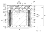
- FIG. 11 schematically illustrates an example of a layered cross-sectional configuration of a photodetector 2A as a first modified example according to the second embodiment of the present disclosure.
- the photodetector 2A is such that the wiring layer 181 and the body portion 52 each have a two-layer structure.
- the configuration of the photodetector 2A is substantially the same as the configuration of the photodetector 2 except for this point.
- the body portion 52 extending parallel to the XY plane has two layers: a first layer 52A in contact with the upper end of the lead-out portion 53 and a second layer 52B that covers the first layer 52A and contacts the via V2. It has a layered structure.
- the wiring layer 181 has a two-layer structure of a first layer 181A in contact with the upper end of the via V1 and a second layer 181B covering the first layer 181A and in contact with the via V2.
- the first layer 52A and the first layer 181A are preferably made of the same material, have the same thickness, and are positioned on substantially the same level.
- the first layer 52A and the first layer 181A are, for example, WSi (tungsten silicon) layers.
- the second layer 52B and the second layer 181B are preferably made of the same material, have the same thickness, and are positioned on substantially the same level.
- the second layer 52B and the second layer 181B are, for example, W (tungsten) layers.
- the lead-out portion 53 and the via V1 made of polysilicon are in contact with the first layer 52A and the first layer 181A, which are WSi (tungsten silicon) layers.
- the extraction portion 53 and the via V1 made of polysilicon are in contact with the body portion 52 and the first layer 181 made of W (tungsten), respectively. there is Therefore, the contact resistance between the extraction portion 53 and the main body portion 52 and the contact resistance between the via V1 and the wiring layer 181 can be stabilized at a lower level than in the photodetector 2 of the second embodiment.
- FIG. 12 schematically illustrates an example of a laminated cross-sectional configuration of a photodetector 2B as a second modified example according to the second embodiment of the present disclosure.
- the photodetector 2B has a via V2 arranged directly above the lead-out portion 53 of the resistive element 51. As shown in FIG. That is, the take-out portion 53 and the via V2 provided on the main body portion 52 are provided at positions overlapping each other in the Z-axis direction.
- the configuration of the photodetector 2B is substantially the same as the configuration of the photodetector 2 except for this point.
- the via V2 is provided directly above the take-out portion 53, so that the dimension of the body portion 52 in the XY plane direction can be further reduced.
- FIG. 13A schematically illustrates an example of a laminated cross-sectional configuration of a photodetector 2C as a third modified example according to the second embodiment of the present disclosure.
- FIG. 13B is a schematic diagram showing a planar configuration example (planar layout) of the photodetector 2C shown in FIG. 13A. Note that FIG. 13A shows a cross section in the arrow direction along the XIIIA-XIIIA cutting line shown in FIG. 13B. Also, FIG. 13B shows an XY cross section of a layer including the reflective layer 41 and the like.
- the photodetector 2C further includes a plurality of reflective layers 41 as shown in FIGS. 13A and 13B. Except for this point, the configuration of the photodetector 2C is the same as that of the photodetector 2B.
- a plurality of reflective layers 41 are discretely arranged along the XY plane. Specifically, the plurality of reflective layers 41 are arranged two-dimensionally periodically to form a check pattern along the XY plane. That is, a gap is provided between the reflective layers 41 adjacent to each other in the X-axis direction and the Y-axis direction.
- the multiple reflective layers 41 are provided on the same layer as the main body 52 and the wiring layer 181 , for example.
- the multiple reflective layers 41 are made of a polycrystalline semiconductor such as polysilicon.
- the body portion 52 and the wiring layer 181 are preferably made of the same kind of constituent material as the constituent material of the reflective layer 41 (the same kind of polycrystalline semiconductor such as polysilicon). This is because the reflective layer 41, the body portion 52, and the wiring layer 181 can be formed collectively.
- the photodetector 2C of this modified example since a plurality of reflective layers 41 are provided, the light that is incident from the second surface 11S2 and has passed through the light receiving section 13 is reflected, can be made incident on Therefore, higher photodetection sensitivity can be obtained.
- FIG. 14A schematically illustrates an example of a laminated cross-sectional configuration of a photodetector 2D as a fourth modified example according to the second embodiment of the present disclosure.
- FIG. 14B is a schematic diagram showing a planar configuration example (planar layout) of the photodetector 2D shown in FIG. 14A. It should be noted that FIG. 14A represents a cross section in the arrow direction along the XIVA-XIVA cutting line shown in FIG. 14B.
- the photodetector 2C further includes a plurality of reflective layers 41 and a plurality of reflective layers 42, as shown in FIGS. 14A and 14B. Except for this point, the configuration of the photodetector 2D is the same as that of the photodetector 2B.
- a plurality of reflective layers 41 are discretely arranged along the XY plane. Specifically, the plurality of reflective layers 41 are arranged two-dimensionally periodically to form a check pattern along the XY plane. That is, a gap is provided between the reflective layers 41 adjacent to each other in the X-axis direction and the Y-axis direction. In the photodetector 2 ⁇ /b>D, the multiple reflective layers 41 are provided on the same layer as the main body 52 and the wiring layer 181 , for example.
- the multiple reflective layers 41 are made of a polycrystalline semiconductor such as polysilicon.
- the body portion 52 and the wiring layer 181 are preferably made of the same kind of constituent material as the constituent material of the reflective layer 41 (the same kind of polycrystalline semiconductor such as polysilicon). This is because the reflective layer 41, the body portion 52, and the wiring layer 181 can be formed collectively.
- a plurality of reflective layers 42 are also arranged discretely along the XY plane. Specifically, the plurality of reflective layers 42 are arranged two-dimensionally periodically to form a check pattern along the XY plane. However, the plurality of reflective layers 42 are on a layer different from the layer on which the plurality of reflective layers 41 are provided, and are provided at positions that fill gap regions between the plurality of reflective layers 41 in the XY plane. That is, the multiple reflective layers 42 are provided at positions corresponding to the gaps between the multiple reflective layers 41 in the thickness direction (Z-axis direction). The multiple reflective layers 42 are embedded in the semiconductor layer 15, for example. The plurality of reflective layers 42 may be made of SiO2, for example.
- the plurality of reflective layers 41 and the plurality of reflective layers 42 are provided.
- the light can be efficiently reflected and made incident on the light receiving section 13 again. Therefore, even higher photodetection sensitivity can be obtained.
- the via V1 and the take-out portion 53 are made of a polycrystalline semiconductor material such as polysilicon, while the wiring layer 181 and the body portion 52 are made of a metal material such as tungsten. It was made to consist of However, the present disclosure is not so limited.
- the wiring layer 181 and the body portion 52 in addition to the via V1 and the extraction portion 53 may be made of a polycrystalline semiconductor such as polysilicon. This is because the via V1, the extraction portion 53, the wiring layer 181, and the main body portion 52 can be collectively formed.
- the via V2 is preferably made of W (tungsten) instead of Cu (copper). This is because interdiffusion may occur when polysilicon and Cu are in direct contact with each other. Such interdiffusion can be avoided at the contact interface between polysilicon and W (tungsten).
- FIG. 15 schematically illustrates an example of the cross-sectional configuration of the photodetector 3 according to the third embodiment of the present disclosure.
- 16A and 16B are cross-sectional schematic diagrams showing a first configuration example and a second configuration example, respectively, of the horizontal cross section of the photodetector 3 shown in FIG. 15.
- FIGS. 16A and 16B show horizontal cross sections at positions including the resistance element 51 shown in FIG.
- FIG. 15 shows a cross section in the arrow direction along the XV-XV cutting line shown in FIGS. 16A and 16B.
- the resistive element 51 and the contact layer 16 are electrically connected via the wiring layer 183 as the fourth wiring.
- the wiring layer 183 is provided on the side opposite to the semiconductor substrate 11 when viewed from the resistance element 51 . More specifically, the resistance element 51 is connected to the contact layer 183 via a via V4 connected to the upper end of the contact layer 16, a wiring layer 183, and a via V5 sandwiched between the wiring layer 183 and the resistance element 51. 16 is connected.
- the via V4 extends in the Z-axis direction inside the interlayer insulating layer 182 so as to connect the contact layer 16 and the wiring layer 183 .
- the via V5 is provided in the same layer as the via V2.
- the distance G1 (see FIG. 15) between the lower surface of the resistance element 51 and the upper surface of the contact layer 16, that is, the portion 182A of the interlayer insulating layer 182 sandwiched between the resistance element 51 and the contact layer 16 is The thickness is desirably greater than 150 nm when the dielectric constant ⁇ of the material forming the interlayer insulating layer 182 is 4.2. If the gap (thickness) G1 is even smaller than this, a strong electric field is generated at an unintended location between the main body portion 52 and the multiplier portion 14, that is, at a location other than the first connection portion C1, resulting in unintended avalanche of electrons. This is because multiplication may occur.
- the resistance element 51 has resistance portions 51A to 51D extending substantially linearly along the XY plane and connected to each other by connection portions 56A to 56C made of copper or the like. be.
- the resistance portions 51A to 51D are made of polycrystalline semiconductor such as polysilicon.
- the resistance element 51 has only the resistance portions 51A to 51D extending substantially linearly. Easy to control resistance value.
- the resistive element 51 may have a shape that circles along the inner edge of the pixel separating portion 17 that partitions the pixel P in the XY plane.
- the path length of the resistance element 51 can be lengthened, and a larger resistance value can be obtained in a limited area.
- it is somewhat difficult to obtain a desired resistance value because the resistance element 51 includes a bent portion.
- FIG. 17 schematically illustrates an example of a laminated cross-sectional configuration of a photodetector 3A as a first modified example according to the third embodiment of the present disclosure.
- the resistive element 51 includes two or more resistive layers 51-1 and 51-2 provided on different layers.
- the configuration of the photodetector 3A is substantially the same as the configuration of the photodetector 3 except for this point.
- the resistive element 51 is composed of a resistive layer 51-1 and a resistive layer 51-2 laminated thereon. Therefore, compared to the photodetector 3 or the like, the resistive element 51 can obtain a larger resistance value without increasing the area occupied in the XY plane.
- a polycrystalline semiconductor such as polysilicon is connected to the cathode as a resistance element, it will have the same potential as the cathode (eg, +3 V), and the potential inside the semiconductor substrate may be modulated. In that case, the withstand voltage of the insulating film between the polysilicon as the resistance element and the semiconductor substrate is lowered. Also, dark current may increase.
- the applicant of the present application has come to provide a highly reliable photodetector that is compatible with miniaturization.
- FIG. 18 schematically illustrates an example of a cross-sectional configuration of the photodetector 4 according to the fourth embodiment of the present disclosure.
- 19A and 19B are schematic diagrams showing first configuration examples and second configuration examples of the planar layout of the photodetector 4 shown in FIG.
- FIGS. 19A and 19B mainly describe the shape, size, and arrangement position of the electrode body 61 (described later) and the resistance element 51, and partially omit other components.
- FIG. 18 shows a cross section in the arrow direction along the XVIII-XVIII cutting line shown in FIGS. 19A and 19B.
- FIG. 20 is a circuit diagram showing an example of an equivalent circuit of the unit pixel P of the photodetector 4 shown in FIG.
- the photodetector 4 further includes an electrode body 61 .
- a voltage different from the voltage applied to the resistance element 51 is applied to the electrode body 61 .
- the polarity of the voltage applied to the electrode body 61 is preferably opposite to the polarity of the voltage applied to the resistance element 51 .
- a voltage of +3 V is applied to the resistance element 51
- a voltage of -3 V for example, from the power supply voltage VDD2 (see FIG. 20) is applied to the electrode body 61 via the via V6 (see FIGS. 19A and 19B).
- the constituent material of the electrode body 61 may be the same as the constituent material of the resistance element 51, for example.
- the electrode body 61 can be made of a polycrystalline semiconductor such as polysilicon.
- the electrode body 61 may be made of a metal material such as W (tungsten) or Cu (copper).
- the gap G2 between the electrode body 61 and the first surface 15S1 is preferably narrower than the gap G1 between the resistance element 51 and the first surface 15S1.
- the resistance element 51 has, for example, four resistance portions 51A to 51D each having a rectangular planar shape extending in the Y-axis direction.
- the four resistance portions 51A-51D are connected in series with each other via connection portions 56A-56C made of copper or the like.
- two electrode bodies 61A and 61B are provided as the electrode body 61 .
- Each of the electrode bodies 61A and 61B has, for example, a rectangular planar shape extending in the Y-axis direction, like the resistor portions 51A to 51D.
- the electrode body 61A is provided, for example, between the resistance portion 51A and the pixel separating portion 17 in the light receiving region in which the light receiving portion 13 is provided. Further, the electrode body 61B is provided, for example, between the resistance portion 51D and the pixel separating portion 17 in the light receiving region in which the light receiving portion 13 is provided.
- each of the electrode bodies 61C and 61D has a rectangular planar shape extending in the X-axis direction.
- the electrode bodies 61C and 61D are provided, for example, in the gaps between the four resistance portions 51A to 51D and the pixel separating portion 17 in the light receiving region in which the light receiving portion 13 is provided.
- the photodetector 4 of the present embodiment further includes an electrode body provided at a position facing the first surface 11S1 and to which a voltage different from the voltage applied to the resistance element 51 can be applied. Therefore, compared to the configuration in which the electrode body 61 is not provided as in the photodetector 3 of the above-described third embodiment, the potential modulation inside the semiconductor substrate 11 in the direction along the first surface 11S1. can be suppressed. As a result, sufficient withstand voltage is ensured without increasing the thickness of the insulating layer 182A provided between the resistance element 51 and the contact layer 16.
- the resistance element 51 can be provided in the region of the light receiving section 13 instead of the region of the pixel separation section 17. can be done. Therefore, in the photodetector 4, a sufficiently large area for the light receiving portion 13 can be secured, and sufficient light receiving sensitivity can be obtained.
- the electrode body 61 at a position facing the first surface 11S1 on the side opposite to the light incident surface of the semiconductor substrate 11, the photons transmitted through the semiconductor substrate 11 are reflected and diffused, and the photons transmitted through the semiconductor substrate 11 are reflected and diffused again. Photons can be incident on the light receiving section 13 . That is, the length of the path along which photons reentering the light receiving section 13 of the semiconductor substrate 11 travel, that is, the actual optical path length inside the light receiving section 13 is longer than when the electrode body 61 is not provided. Therefore, in the photodetector 4, the quantum efficiency is improved and the light receiving sensitivity is improved.
- the interlayer insulating layer between the resistance element 51 and the first surface 15S1 It is possible to more effectively suppress potential modulation inside the semiconductor substrate 11 while sufficiently ensuring the withstand voltage of the portion 182A of the portion 182 .
- FIG. 21A schematically illustrates an example of a planar layout of a photodetector 4A as a first modified example according to the fourth embodiment of the present disclosure.
- the photodetector 4A six electrode bodies 61A to 61F each extending in the Y-axis direction are arranged in the X-axis direction.
- resistance portions 51A to 51D that extend in the Y-axis direction and constitute the resistance element 51 are provided.
- Resistive portion 51A is disposed between electrode body 61A and all pole body 61B
- resistive portion 51B is disposed between electrode body 61B and all pole body 61C
- resistive portion 51C is disposed between electrode body 61D and all pole body 61E.
- the resistive portion 51D is arranged between the electrode body 61E and the total pole body 61F.
- FIG. 21B schematically illustrates an example of a planar layout of a photodetector 4B as a second modified example according to the fourth embodiment of the present disclosure.
- one electrode body 61 is provided in an annular shape along the outer edge of the light receiving section 13 .
- FIG. 21C schematically illustrates an example of a planar layout of a photodetector 4C as a third modified example according to the fourth embodiment of the present disclosure.
- the photodetector 4C includes one electrode body 61 having a spirally wound planar shape and one resistance element 51 having a spirally wound planar shape.
- the plurality of wound portions of the electrode body 61 are arranged in the gaps between the plurality of wound portions of the resistive element 51 .
- the applicant has come to provide a semiconductor device having a resistance element that can be adapted to high integration, and a method of manufacturing the same.
- FIG. 22 schematically illustrates an example of the cross-sectional configuration of the photodetector 5 according to the fifth embodiment of the present disclosure.
- FIG. 23 is an enlarged cross-sectional view showing an enlarged part of the photodetector 5 shown in FIG.
- the structure of the resistance element 51 is different from that of the photodetector 2B described in the second embodiment, for example.
- the configuration of the photodetector 5 is substantially the same as the configuration of the photodetector 2B (FIG. 12) except for the above points.
- the resistive element 51 has resistive portions 51A to 51E.
- the resistance portions 51A, 51C, 51E and the resistance portions 51B, 51D are provided at different height positions in the Z-axis direction.
- the resistance portions 51A, 51C, 51E are formed on the first surface 15S1 of the semiconductor layer 15.
- the resistance portions 51B and 51D are formed on the convex portion 182T forming part of the insulating layer 182.
- the convex portion 182T is provided between the resistance portion 51A and the resistance portion 51C and between the resistance portion 51C and the resistance portion 51E in the X-axis direction.
- a resistance portion 51B is provided between the resistance portions 51A and 51C
- a resistance portion 51D is provided between the resistance portions 51C and 51E.
- FIG. 24 shows a configuration example of a planar layout of the resistance element 51.
- FIG. Each of the resistance portions 51A to 51E has a rectangular planar shape extending in the Y-axis direction.
- the resistance portions 51A to 51E are laid out without gaps in the X-axis direction in plan view.
- the resistance portions 51A, 51C, 51E and the resistance portions 51B, 51D are provided at different height positions in the Z-axis direction. , and the resistance portions 51B and 51D are separated from each other without being in direct contact with each other.
- the resistance portions 51A-51E are connected in series by connection portions 56A-56D.
- connection portion 56A connects the resistance portion 51C and the resistance portion 51E
- connection portion 56B connects the resistance portion 51E and the resistance portion 51D
- connection portion 56C connects the resistance portion 51D and the resistance portion 51B
- connection portion 56D connects the resistance portion 51D and the resistance portion 51B. It connects the portion 51B and the resistance portion 51A. Therefore, the resistance portions 51A to 51E are integrated as the resistance element 51.
- a connection portion 56E is provided at the opposite end of the resistance portion 51A to the connection portion 56D.
- the resistance portion 51A is connected to the readout circuit 75 via the connection portion 56E. It is desirable that the thicknesses of the resistance portions 51A to 51E are constant in the XY plane and equal to each other.
- FIGS. 25A to 25I are schematic cross-sectional views of laminated layers representing one step of the method of manufacturing the resistive element 51 of the photodetector 5, respectively.
- an insulating film 182Z1 is formed on the semiconductor layer 15. Then, as shown in FIG. 25A, an insulating film 182Z1 is formed on the semiconductor layer 15. Then, as shown in FIG. 25A, an insulating film 182Z1 is formed on the semiconductor layer 15. Then, as shown in FIG. 25A, an insulating film 182Z1 is formed on the semiconductor layer 15. Then, as shown in FIG. 25A, an insulating film 182Z1 is formed on the semiconductor layer 15. Then, as shown in FIG.
- a resist layer 182R1 is formed on the insulating film 182Z1.
- a resist pattern 182RP1 having openings K182R1 at predetermined positions is formed by photolithography.
- an etching process is performed using the resist pattern 182RP1 as a mask to select a portion of the insulating film 182Z1 that is exposed without being covered with the resist pattern 182RP1, that is, a portion corresponding to the opening K182R1. effectively remove. Thereby, a plurality of convex portions 182T are formed. At this time, the first surface 15S1 of the semiconductor layer 15 is exposed between the plurality of protrusions 182T.
- a resistive film 51Z is formed so as to cover the plurality of protrusions 182T and the entire exposed first surface 15S1.
- the resistive film 51Z is formed by, for example, a CVD (chemical vapor deposition) method, a PVD (Physical Vapor Deposition) method, or the like, using a polycrystalline semiconductor material such as polysilicon.
- CVD chemical vapor deposition
- PVD Physical Vapor Deposition
- an insulating film 182Z2 is formed so as to entirely cover the resistive film 51Z.
- isotropic etching is performed to remove the portion of the insulating film 182Z2 that covers the side surface of the projection 182T.
- the resistive film 51Z covering the side surface of the projection 182T is removed.
- the resistive film 51Z is separated into resistive portions 51A to 51E. That is, the resistance portions 51A, 51C, and 51E are formed in a self-aligning manner so as to match the widths W1, W3, and W5 of the regions where the first surface 15S1 is exposed without the protrusion 182T.
- the resistance portions 51B and 51D are formed in a self-aligning manner so as to match the widths W2 and W4 of the projections 182T1 and 182T2, respectively. Therefore, the sum of the widths W1 to W5 of the resistance portions 51A to 51E matches the width W51 of the area occupied by the resistance element 51.
- FIG. 25I after obtaining the insulating layer 182 by forming the insulating layer 182Z3 so as to cover the entire surface, the via V7 and the connecting portions 56A to 56E are formed to form the resistance portion 51A. 51E are connected to each other to complete the resistive element 51.
- FIG. 25I after obtaining the insulating layer 182 by forming the insulating layer 182Z3 so as to cover the entire surface, the via V7 and the connecting portions 56A to 56E are formed to form the resistance portion 51A. 51E are connected to each other to complete the resistive element 51.
- the resistance element 51 is formed such that the resistance portions adjacent to each other in the X-axis direction are formed at different height positions. Therefore, the plurality of resistance portions 51A to 51E can be arranged without gaps in the X-axis direction. As a result, more resistance portions can be formed within a region of a given area. That is, the resistance value of the resistance element 51 formed within a region of a certain area can be further increased. Therefore, according to the photodetector 5, it is possible to cope with further high integration.
- the resistance element 51 has a structure in which a plurality of resistance portions 51A to 51E constituting the resistance element 51 can be collectively formed. For this reason, compared with the case of forming the plurality of resistance portions 51A to 51E individually, for example, the manufacturing efficiency is high, and variations in film thickness and film quality of the plurality of resistance portions 51A to 51E can be suppressed. Furthermore, even if the widths (dimensions in the X-axis direction) of the resistance portions 51A to 51E are different from each other, the total width of the resistance portions 51A to 51E is brought close to a constant value, thereby increasing the resistance value of the resistance element 51 as a whole. Variation can be reduced.
- FIG. 26 is an enlarged cross-sectional view showing an enlarged part of a photodetector 5A as a first modified example according to the fifth embodiment of the present disclosure.
- the resistive element 51 has resistive portions 51A to 51E.
- the resistor portions 51A to 51E are provided in a layer between the semiconductor layer 15 and an insulating layer 182E forming a part of the insulating layer 182, and extend in the Y-axis direction like the photodetector 5. are doing.
- the resistance portions 51A, 51C, 51E and the resistance portions 51B, 51D are provided at different height positions in the Z-axis direction.
- the resistance portions 51A, 51C, 51E are formed on the first surface 15S1 of the semiconductor layer 15.
- the resistance portions 51B and 51D are formed on an insulating layer 182D forming part of the insulating layer 182.
- the resistance portions 51B and 51D are separated from the first surface 15S1 of the semiconductor layer 15 by the thickness of the insulating layer 182D. That is, the height positions of the lower surfaces of the resistance portions 51A, 51C, 51E and the height positions of the lower surfaces of the resistance portions 51B, 51D are shifted by the thickness of the insulating layer 182D.
- the insulating layer 182D is provided so as to fill the gaps between the resistance portions 51A to 51E. It is desirable that the thicknesses of the resistance portions 51A to 51E are constant in the XY plane and equal to each other.
- the resistive element 51 of the photodetector 5A as this modified example, a gap corresponding to the thickness of the insulating layer 182D is generated between the resistive portions adjacent to each other in the X-axis direction.
- the resistance portions 51A to 51E are formed on substantially the same layer as each other. That is, when viewed in the X-axis direction, the resistance portions 51A to 51E are provided at positions where at least portions of the resistance portions 51A to 51E overlap in the layer between the semiconductor layer 15 and the insulating layer 182E. . Therefore, in the photodetector 5A, the thickness of the resistive element 51 is made thinner than in the photodetector 5A. Therefore, the embodiment of the photodetector 5A is more suitable for further thinning.
- FIGS. 27A to 27F are schematic cross-sectional views of laminated layers representing one step of the method of manufacturing the resistive element 51 of the photodetector 5A.
- a resistive film 51Z1 is formed entirely on the semiconductor layer 15. Then, as shown in FIG. 27A, a resistive film 51Z1 is formed entirely on the semiconductor layer 15. Then, as shown in FIG. The resistive film 51Z1 is formed by CVD or PVD using a polycrystalline semiconductor material such as polysilicon. Thereafter, a resist layer 182R1 is formed over the entire surface of the resistive film 51Z1.
- a resist pattern 182RP2 having openings K182R2 at predetermined positions is formed by photolithography.
- an etching process is performed using the resist pattern 182RP2 as a mask to select a portion of the resistive film 51Z1 that is exposed without being covered with the resist pattern 182RP2, that is, a portion corresponding to the opening K182R2. effectively remove. Thereby, resistance portions 51A, 51C and 51E are formed. At this time, the first surface 15S1 of the semiconductor layer 15 is exposed in the gaps between the resistor portions 51A, 51C, 51E.
- an insulating film 182D is formed to entirely cover the resistance portions 51A, 51C, 51E and the first surface 15S1 of the semiconductor layer 15, as shown in FIG. 27D.
- a resistive film 51Z2 is formed to entirely cover the insulating film 182D.
- the entire surface is polished by CMP or the like to remove protruding portions of the resistance film 51Z2 until the insulating film 182D covering the resistance portions 51A, 51C and 51E is exposed.
- a resistance portion 51B is formed between the resistance portions 51A and 51C
- a resistance portion 51D is formed between the resistance portions 51C and 51E.
- the photodetector device 5A of this modified example can also cope with higher integration.
- FIG. 28 is an enlarged cross-sectional view showing an enlarged part of a photodetector 5B as a second modified example according to the fifth embodiment of the present disclosure.
- an uneven structure 182TU having alternating convex portions 182T and concave portions 182U is provided on the first surface 15S1 of the semiconductor layer 15.
- the concave portion 182U is provided with resistance portions 51A, 51C, and 51E
- the convex portion 182T is provided with resistance portions 51B and 51D.
- the resistance portions 51A to 51E are provided in the concave-convex structure 182TU. It is held by the uneven structure 182TU.
- FIG. 29 is an enlarged cross-sectional view showing an enlarged part of a photodetector 5C as a third modified example according to the fifth embodiment of the present disclosure.
- each of the resistance portions 51A to 51E is connected to the wiring layer 184 through the via V7, and further connected to the wiring layer 185 through the via V8.
- the vias V7 and V8 and the wiring layers 184 and 185 are formed with predetermined resistance materials, respectively, a higher resistance structure including the resistance element 51, the vias V7 and V8 and the wiring layers 184 and 185 can be formed. .
- FIG. 30 is an enlarged cross-sectional view showing an enlarged part of a photodetector 5D as a fourth modified example according to the fifth embodiment of the present disclosure.
- the resistance portions 51A to 51E are provided at three different height positions. Specifically, in the Z-axis direction, the resistance portions 51A and 51E are provided at the lowest position, the resistance portion 51C is provided at the highest position, and the resistance portions 51B and 51D are provided at an intermediate height position. ing.
- FIG. 31 is an enlarged cross-sectional view showing an enlarged part of a photodetector 5E as a fifth modified example according to the fifth embodiment of the present disclosure.
- the resistive element 51 has a two-layer structure. Specifically, the resistance portions 51F to 51J are formed in the first layer, and the resistance portions 51A to 51E are formed in the second layer. The resistance portions 51F to 51J and the resistance portions 51A to 51E are connected in series to form one resistance element 51.
- the photodetector 5 has a rectangular planar shape in which the resistive portions 51A to 51E each extend in one direction, the present disclosure is not limited to this.
- 32A and 32B are a plan view and a cross-sectional view schematically showing a resistive element 51 that constitutes a photodetector 5F as a sixth modification according to the fifth embodiment of the present disclosure.
- the resistance portions 51B to 51E forming the resistance element 51 are annular patterns having circular outer and inner edges, respectively, and are arranged concentrically around the resistance portion 51A.
- FIG. 33 is a plan view schematically showing a resistive element 51 that configures a photodetector 5G as a seventh modification according to the fifth embodiment of the present disclosure.
- the resistance portions 51B to 51E forming the resistance element 51 are annular patterns each having a rectangular outer edge and inner edge, and are arranged concentrically around the resistance portion 51A.
- FIG. 34 illustrates an example of a schematic configuration of a distance imaging device 1000 as an electronic device including the photodetector (for example, photodetector 1) of the present disclosure.
- the range imaging device 1000 is a specific example corresponding to the "ranging device" of the present disclosure.
- the distance imaging device 1000 has, for example, a light source device 1100, an optical system 1200, a photodetector device 1, an image processing circuit 1300, a monitor 1400, and a memory 1500.
- the distance imaging device 1000 projects light from the light source device 1100 toward the object to be irradiated 2000 and receives light (modulated light or pulsed light) reflected from the surface of the object to be irradiated 2000 . It is possible to acquire a distance image corresponding to the distance of .
- the optical system 1200 includes one or more lenses, guides the image light (incident light) from the irradiation object 2000 to the photodetector 1, and directs it to the light receiving surface (sensor section) of the photodetector 1. to form an image.
- the image processing circuit 1300 performs image processing for constructing a distance image based on the distance signal supplied from the photodetector 1, and the distance image (image data) obtained by the image processing is supplied to the monitor 1400. It is displayed, or is supplied to the memory 1500 and stored (recorded).
- the distance imaging device 1000 configured in this way, by applying the above-described photodetector (for example, the photodetector 1), the irradiation object 2000 can be detected based only on the light reception signal from the unit pixel P with high stability. It is possible to calculate the distance to and generate a highly accurate distance image. That is, the distance imaging device 1000 can acquire a more accurate distance image.
- the photodetector for example, the photodetector 1
- the technology according to the present disclosure can be applied to various products.
- the technology according to the present disclosure can be applied to any type of movement such as automobiles, electric vehicles, hybrid electric vehicles, motorcycles, bicycles, personal mobility, airplanes, drones, ships, robots, construction machinery, agricultural machinery (tractors), etc. It may also be implemented as a body-mounted device.
- FIG. 35 is a block diagram showing a schematic configuration example of a vehicle control system, which is an example of a mobile control system to which the technology according to the present disclosure can be applied.
- a vehicle control system 12000 includes a plurality of electronic control units connected via a communication network 12001.
- the vehicle control system 12000 includes a drive system control unit 12010, a body system control unit 12020, an outside information detection unit 12030, an inside information detection unit 12040, and an integrated control unit 12050.
- a microcomputer 12051, an audio/image output section 12052, and an in-vehicle network I/F (interface) 12053 are illustrated.
- the drive system control unit 12010 controls the operation of devices related to the drive system of the vehicle according to various programs.
- the driving system control unit 12010 includes a driving force generator for generating driving force of the vehicle such as an internal combustion engine or a driving motor, a driving force transmission mechanism for transmitting the driving force to the wheels, and a steering angle of the vehicle. It functions as a control device such as a steering mechanism to adjust and a brake device to generate braking force of the vehicle.
- the body system control unit 12020 controls the operation of various devices equipped on the vehicle body according to various programs.
- the body system control unit 12020 functions as a keyless entry system, a smart key system, a power window device, or a control device for various lamps such as headlamps, back lamps, brake lamps, winkers or fog lamps.
- body system control unit 12020 can receive radio waves transmitted from a portable device that substitutes for a key or signals from various switches.
- the body system control unit 12020 receives the input of these radio waves or signals and controls the door lock device, power window device, lamps, etc. of the vehicle.
- the vehicle exterior information detection unit 12030 detects information outside the vehicle in which the vehicle control system 12000 is installed.
- the vehicle exterior information detection unit 12030 is connected with an imaging section 12031 .
- the vehicle exterior information detection unit 12030 causes the imaging unit 12031 to capture an image of the exterior of the vehicle, and receives the captured image.
- the vehicle exterior information detection unit 12030 may perform object detection processing or distance detection processing such as people, vehicles, obstacles, signs, or characters on the road surface based on the received image.
- the imaging unit 12031 is an optical sensor that receives light and outputs an electrical signal according to the amount of received light.
- the imaging unit 12031 can output the electric signal as an image, and can also output it as distance measurement information.
- the light received by the imaging unit 12031 may be visible light or non-visible light such as infrared rays.
- the in-vehicle information detection unit 12040 detects in-vehicle information.
- the in-vehicle information detection unit 12040 is connected to, for example, a driver state detection section 12041 that detects the state of the driver.
- the driver state detection unit 12041 includes, for example, a camera that captures an image of the driver, and the in-vehicle information detection unit 12040 detects the degree of fatigue or concentration of the driver based on the detection information input from the driver state detection unit 12041. It may be calculated, or it may be determined whether the driver is dozing off.
- the microcomputer 12051 calculates control target values for the driving force generator, the steering mechanism, or the braking device based on the information inside and outside the vehicle acquired by the vehicle exterior information detection unit 12030 or the vehicle interior information detection unit 12040, and controls the drive system control unit.
- a control command can be output to 12010 .
- the microcomputer 12051 realizes the functions of ADAS (Advanced Driver Assistance System) including collision avoidance or shock mitigation, follow-up driving based on inter-vehicle distance, vehicle speed maintenance driving, vehicle collision warning, or vehicle lane deviation warning. Cooperative control can be performed for the purpose of ADAS (Advanced Driver Assistance System) including collision avoidance or shock mitigation, follow-up driving based on inter-vehicle distance, vehicle speed maintenance driving, vehicle collision warning, or vehicle lane deviation warning. Cooperative control can be performed for the purpose of ADAS (Advanced Driver Assistance System) including collision avoidance or shock mitigation, follow-up driving based on inter-vehicle distance, vehicle speed maintenance driving, vehicle collision warning, or vehicle
- the microcomputer 12051 controls the driving force generator, the steering mechanism, the braking device, etc. based on the information about the vehicle surroundings acquired by the vehicle exterior information detection unit 12030 or the vehicle interior information detection unit 12040, so that the driver's Cooperative control can be performed for the purpose of autonomous driving, etc., in which vehicles autonomously travel without depending on operation.
- the microcomputer 12051 can output a control command to the body system control unit 12020 based on the information outside the vehicle acquired by the information detection unit 12030 outside the vehicle.
- the microcomputer 12051 controls the headlamps according to the position of the preceding vehicle or the oncoming vehicle detected by the vehicle exterior information detection unit 12030, and performs cooperative control aimed at anti-glare such as switching from high beam to low beam. It can be carried out.
- the audio/image output unit 12052 transmits at least one of audio and/or image output signals to an output device capable of visually or audibly notifying the passengers of the vehicle or the outside of the vehicle.
- an audio speaker 12061, a display unit 12062, and an instrument panel 12063 are illustrated as output devices.
- the display unit 12062 may include at least one of an on-board display and a head-up display, for example.
- FIG. 36 is a diagram showing an example of the installation position of the imaging unit 12031.
- the imaging unit 12031 has imaging units 12101, 12102, 12103, 12104, and 12105.
- the imaging units 12101, 12102, 12103, 12104, and 12105 are provided at positions such as the front nose of the vehicle 12100, the side mirrors, the rear bumper, the back door, and the upper part of the windshield in the vehicle interior, for example.
- An image pickup unit 12101 provided in the front nose and an image pickup unit 12105 provided above the windshield in the passenger compartment mainly acquire images in front of the vehicle 12100 .
- Imaging units 12102 and 12103 provided in the side mirrors mainly acquire side images of the vehicle 12100 .
- An imaging unit 12104 provided in the rear bumper or back door mainly acquires an image behind the vehicle 12100 .
- the imaging unit 12105 provided above the windshield in the passenger compartment is mainly used for detecting preceding vehicles, pedestrians, obstacles, traffic lights, traffic signs, lanes, and the like.
- FIG. 36 shows an example of the imaging range of the imaging units 12101 to 12104.
- the imaging range 12111 indicates the imaging range of the imaging unit 12101 provided in the front nose
- the imaging ranges 12112 and 12113 indicate the imaging ranges of the imaging units 12102 and 12103 provided in the side mirrors, respectively
- the imaging range 12114 The imaging range of an imaging unit 12104 provided in the rear bumper or back door is shown. For example, by superimposing the image data captured by the imaging units 12101 to 12104, a bird's-eye view image of the vehicle 12100 viewed from above can be obtained.
- At least one of the imaging units 12101 to 12104 may have a function of acquiring distance information.
- at least one of the imaging units 12101 to 12104 may be a stereo camera composed of a plurality of imaging elements, or may be an imaging element having pixels for phase difference detection.
- the microcomputer 12051 determines the distance to each three-dimensional object within the imaging ranges 12111 to 12114 and changes in this distance over time (relative velocity with respect to the vehicle 12100). , it is possible to extract, as the preceding vehicle, the closest three-dimensional object on the course of the vehicle 12100, which runs at a predetermined speed (for example, 0 km/h or more) in substantially the same direction as the vehicle 12100. can. Furthermore, the microcomputer 12051 can set the inter-vehicle distance to be secured in advance in front of the preceding vehicle, and perform automatic brake control (including following stop control) and automatic acceleration control (including following start control). In this way, cooperative control can be performed for the purpose of automatic driving in which the vehicle runs autonomously without relying on the operation of the driver.
- automatic brake control including following stop control
- automatic acceleration control including following start control
- the microcomputer 12051 converts three-dimensional object data related to three-dimensional objects to other three-dimensional objects such as motorcycles, ordinary vehicles, large vehicles, pedestrians, and utility poles. It can be classified and extracted and used for automatic avoidance of obstacles. For example, the microcomputer 12051 distinguishes obstacles around the vehicle 12100 into those that are visible to the driver of the vehicle 12100 and those that are difficult to see. Then, the microcomputer 12051 judges the collision risk indicating the degree of danger of collision with each obstacle, and when the collision risk is equal to or higher than the set value and there is a possibility of collision, an audio speaker 12061 and a display unit 12062 are displayed. By outputting an alarm to the driver via the drive system control unit 12010 and performing forced deceleration and avoidance steering via the drive system control unit 12010, driving support for collision avoidance can be performed.
- At least one of the imaging units 12101 to 12104 may be an infrared camera that detects infrared rays.
- the microcomputer 12051 can recognize a pedestrian by determining whether or not the pedestrian exists in the captured images of the imaging units 12101 to 12104 .
- recognition of a pedestrian is performed by, for example, a procedure for extracting feature points in images captured by the imaging units 12101 to 12104 as infrared cameras, and performing pattern matching processing on a series of feature points indicating the outline of an object to determine whether or not the pedestrian is a pedestrian.
- the audio image output unit 12052 outputs a rectangular outline for emphasis to the recognized pedestrian. is superimposed on the display unit 12062 . Also, the audio/image output unit 12052 may control the display unit 12062 to display an icon or the like indicating a pedestrian at a desired position.
- the content of the present disclosure is not limited to the above-described embodiments and the like, and various modifications are possible.
- the photodetector of the present disclosure need not include all of the constituent elements described in the above embodiments and the like, and conversely, may include other layers.
- polysilicon was exemplified as the polycrystalline semiconductor that constitutes the resistance element, but in the present disclosure, other polycrystalline semiconductors may be used to constitute the resistor.
- both the main body portion 52 and the extraction portion 53 of the resistance element 51 are made of polycrystalline semiconductor, but the present disclosure is not limited to this.
- part or all of the body portion 52 may be replaced with a cermet resistor, and part of the extraction portion 53 may be replaced with a cermet resistor.
- a portion of the lead-out portion 53 that constitutes the first connection portion C1 connected to the contact layer 16 is made of a polycrystalline semiconductor.
- the p-type semiconductor region (p+) 113 which is the anode, is connected to the via V1 on the first surface 11S1 of the semiconductor substrate 11, and the wiring layer 181 and the like are connected. is used to secure a conduction path between the anode and the outside.
- the connection with the p-type semiconductor region (p+) 113, which is the anode may be made on the second surface 11S2 of the semiconductor substrate 11.
- the polarities of the semiconductor regions forming the photodetector of the present disclosure may be reversed.
- the photodetector of the present disclosure may use holes as signal charges.
- the respective potentials are not limited as long as avalanche multiplication is caused by applying a reverse bias between the anode and the cathode.
- the semiconductor substrate 11 and the semiconductor layer 15 may be, for example, germanium (Ge) or silicon (Si) and germanium ( Ge) and compound semiconductors (eg, silicon germanium (SiGe)) can also be used.
- a resistor made of a polycrystalline semiconductor material is connected to the first electrode electrically connected to the multiplier section. Therefore, the structural stability of the semiconductor substrate is higher than when the resistor is made of metal. That is, since it is possible to suppress the occurrence of crystal structure defects in the semiconductor substrate, it is possible to obtain high reliability of the semiconductor substrate 11, such as ensuring a sufficient withstand voltage.
- the present disclosure may be configured as follows.
- a semiconductor substrate having a first surface and a second surface facing each other and having a pixel array section in which a plurality of pixels are arranged in an array in an in-plane direction; a light receiving unit provided inside the semiconductor substrate for each pixel and configured to generate carriers according to the amount of light received by photoelectric conversion; provided on the first surface of the semiconductor substrate for each of the pixels, has a laminated structure of a first conductivity type region and a second conductivity type region, and avalanche-increases the carriers generated in the light receiving section; a multiplier for doubling; a first electrode electrically connected to the multiplier; a second electrode electrically connected to the light receiving section; A photodetector comprising: a resistor made of a polycrystalline semiconductor material provided so as to face the first surface and be in contact with the first electrode.
- the photodetector according to . (5) The main body portion extends from the central region of the pixel toward the peripheral region of the pixel in a plane parallel to the first plane so that the traveling direction changes in at least one or more locations. 4) The photodetector as described. (6) The photodetector according to (4) above, wherein the body extends spirally from a central region of the pixel toward a peripheral region of the pixel in a plane parallel to the first plane. (7) The photodetector according to (4) above, further comprising a plurality of first reflective layers discretely arranged along the first surface on the same layer as the main body.
- the first electrode is made of a first conductivity type semiconductor containing a first conductivity type impurity element, The photodetector according to any one of (1) to (14) above, wherein the resistor includes the first conductivity type impurity element.
- the resistor has a resistance value of 5 k ⁇ or more.
- the second wiring is made of the polycrystalline semiconductor material;
- the resistor has a body portion extending parallel to the first surface and a lead-out portion connecting the body portion and the first electrode, the second wiring and the extraction portion are made of the polycrystalline semiconductor material;
- the photodetector according to (20) above, wherein the third wiring and the main body are formed of a laminate of a tungsten silicon layer and a tungsten layer.
- (25) a fourth wiring provided on the side opposite to the semiconductor substrate when viewed from the resistor; An insulating film provided between the resistor and the first electrode, The photodetector according to (1), wherein the resistor and the first electrode are electrically connected through the fourth wiring.
- a semiconductor substrate having a first surface and a second surface facing each other and having a pixel array section in which a plurality of pixels are arranged in an array in an in-plane direction; a light receiving unit provided inside the semiconductor substrate for each pixel and configured to generate carriers according to the amount of light received by photoelectric conversion; provided on the first surface of the semiconductor substrate for each of the pixels, has a laminated structure of a first conductivity type region and a second conductivity type region, and avalanche-increases the carriers generated in the light receiving section; a multiplier for doubling; a first electrode electrically connected to the multiplier; a second electrode electrically connected to the light receiving section; a resistor made of a polycrystalline semiconductor material provided so as to be electrically connected to the first electrode at a position facing the first surface; and an electrode body provided at a position facing the first surface and to which a voltage different from the voltage applied to the resistive element can be applied.
- one or more first resistive film portions positioned at a first height in the thickness direction; and at least one second resistive film portion positioned at a second height in the thickness direction and adjacent to the first resistive film portion in a first direction orthogonal to the thickness direction.
- a method of manufacturing a semiconductor device comprising: forming an insulating film made of an insulating material on the semiconductor layer; selectively removing the insulating film to form, on the semiconductor layer, a convex portion made of the insulating material and including a top surface and a side surface; forming a resistive film made of a resistive material so as to cover both the convex portion and a portion of the semiconductor layer surrounding the convex portion; By removing a portion of the resistive film covering the side surface of the protrusion, the first resistive film portion covering the upper surface of the protrusion and the second resistive film portion covering the peripheral portion of the protrusion are formed.
- a method of manufacturing a semiconductor device comprising:
Landscapes
- Solid State Image Pick-Up Elements (AREA)
- Light Receiving Elements (AREA)
- Engineering & Computer Science (AREA)
- Manufacturing & Machinery (AREA)
Abstract
Description
1.第1の実施の形態
(カソード電極を挟んで増倍部と電気的に接続された非金属導電性材料からなる抵抗体を備える光検出装置)
1-0.経緯
1-1.構成
1-2.変形例
1-3.製造方法
1-4.作用・効果
2.第2の実施の形態
2-0.経緯
2-1.構成
2-2.作用・効果
2-3.変形例
3.第3の実施の形態
3-1.構成
3-2.作用・効果
3-3.変形例
4.第4の実施の形態
4-0.経緯
4-1.構成
4-2.作用・効果
4-3.変形例
5.第5の実施の形態
4-0.経緯
4-1.構成
4-2.作用・効果
4-3.変形例
6.適用例
7.応用例
[1-0.経緯]
従来、光を用いたリモートセンシング技術の一つであるLIDAR(Light Detection and Ranging)に適用されるAPD (avalanche photodiode)に関する技術が提案されている(例えば特開2020-150161号公報参照)。LIDARとは、対象物に照射された光の反射光を受光して、対象物までの距離をセンシングする技術もしくはそれを用いた装置である。上記のAPDに関する特許文献(特開2020-150161号公報)には、クエンチ抵抗により、フォトンが入射した際の電子なだれを収束させ、検出感度を上げる技術が公開されている。上記特許文献では、カソードに金属電極を介してクエンチ抵抗を接続する構造が開示されている。ところで上記の技術では、Si基板中に金属電極を形成するため高濃度のn型不純物層が必要となるので、例えばイオン注入による高濃度層の形成が行われる。しかしながら、イオン注入により結晶欠陥が生じる可能性がある。また、金属電極を形成する際にSi基板がダメージを負う可能性もある。そうした可能性はAPDの信頼性低下の要因となる。また、上記特許文献ではグラフェン層によりクエンチ抵抗を構成しているが、クエンチ抵抗として十分な抵抗値を確保するためにある程度の長さが必要となり、微細化を阻害する可能性がある。そこで、本出願人は、小型化に対応しつつ、高い信頼性を有する光検出装置を提供するに至った。
図1は、本開示の第1の実施の形態に係る光検出装置1の断面構成の一例を模式的に表したものである。図2は、図1に示した光検出装置1の概略構成を表したブロック図である。図3Aは、図1に示した光検出装置1の単位画素Pの等価回路の一例を表した回路図である。光検出装置1は、例えば、ToF(Time-of-Flight)法により距離計測を行う距離画像センサ(後述の距離画像装置1000、図34参照)やイメージセンサ等に適用され得る。
図3Aに示したように、単位画素Pは、受光素子12と、保護回路としてのクランプ回路50と、第1の制御トランジスタ71と、電流源72と、端子73と、第2の制御トランジスタ74と、読出し回路75とを備えている。
ンジスタ71は、クランプ回路50を介して受光素子12と直列に接続されている。第1の制御トランジスタ71のソース端子は受光素子12のカソードと接続され、第1の制御トランジスタ71のドレイン端子は電流源72を介して端子73と接続されている。第1の制御トランジスタ71は、ゲート電極に印加されるイネーブル信号ENが低レベルになることで導通状態となり、電流源72からの電流を受光素子12に流すようになっている。第2の制御トランジスタ74は、受光素子12のカソードと基準電位ノード(例えば、グランド)との間に接続されている。第2の制御トランジスタ74は、例えばN型MOSトランジスタからなる。第2の制御トランジスタ74は、イネーブル信号ENと逆相の信号xENがゲート電極に印加されることで導通状態となり、受光素子12に印加される電圧をブレークダウン電圧以下とし、受光素子12を非活性化状態とするようになっている。
発生した過電圧は、例えば、-1V~-3V程度の負電圧にクランプされる。
光検出装置1は、いわゆる裏面照射型の光検出装置である。図1に示したように、光検出装置1は、例えば、センサ基板10の表面(例えば、センサ基板10を構成する半導体基板11の表面である第1面11S1)にロジック基板20が積層されており、センサ基板10の裏面(センサ基板10を構成する半導体基板11の裏面である第2面11S2)から光を受光するようになっている。光検出装置1は、単位画素P毎に受光素子12を有している。受光素子12は、受光部13と増倍部14とを有し、半導体基板11内に受光部13が埋め込み形成されている。半導体基板11にはさらに、第1面11S1に、増倍部14を構成するp型半導体領域(p+)14Xとn型半導体領域(n+)14Yのうちのp型半導体領域(p+)14Xが設けられている。半導体基板11の第1面11S1側には半導体層15が設けられている。半導体層15には、増倍部14を構成するn型半導体領域(n+)14Yが設けられている。
面11S1に平行に延在する、すなわちXY面に沿って延在する本体部52と、本体部52とコンタクト層16とを繋ぐ取り出し部53とを有する。本体部52は、図1に示した構造の例では配線層181と同じ階層に形成されている。但し、抵抗素子51の本体部52は、配線層181と異なる階層に設けられていてもよい。ここで、本体部52の下面とコンタクト層16の上面との距離、すなわち、層間絶縁層182のうち、本体部52とコンタクト層16との間に挟まれた部分の厚みG1(図1参照)は、層間絶縁層182を構成する材料の比誘電率εが4.2であるとき、150nmよりも大きいことが望ましい。これによりも厚みG1が小さい場合、本体部52と増倍部14との間の意図しない箇所、すなわち第1接続部C1以外の箇所で強い電界が生じてしまい、意図しない電子のアバランシェ増倍が生じる可能性があるからである。また、本体部52の上面にはビアV2が立設している。すなわち、抵抗素子51は、ビアV2を介してパッド電極183と電気的に接続されている。但し、例えば本体部52とビアV2との間に配線層181など他の配線層をさらに設けるようにしてもよい。なお、抵抗素子51と接続されたビアV2が本開示の「第1の配線」に対応する一具体例である。
なお、図4Aは、光検出装置1のXY断面の第1の構成例(平面レイアウト)を表す断面模式図である。
なお、図4B~4Eは、光検出装置1のXY断面の第2~5の構成例を表す断面模式図である。
なお、図4Fは、光検出装置1のXY断面の第6の構成例を表す断面模式図である。
うに、本体部52が、互いに異なる体積抵抗率を有する第1~第3部分52-1~52-3を含むようにしてもよい。第1部分52-1は本体部52のうちの取り出し部53と接続される部分であり、第2部分52-2は本体部52のうちのビアV2と接続される部分であり、第3部分52-3は本体部52のうちの第1部分52-1と第2部分52-2とを繋ぐ、長手方向の中央部分である。図4Gの第7の構成例では、例えば第3部分52-3が最も高い体積抵抗率を有し、第1部分52-1および第2部分52-2は第3部分52-3よりも低い体積抵抗率を有するとよい。その場合、例えば第1部分52-1および第2部分52-2におけるn型不純物濃度よりも低いn型不純物濃度を第3部分52-3が有するようにすることで、第3部分52-3の高抵抗化を図るようにしてもよい。あるいは、第3部分52-3にのみp型不純物をイオン注入などにより添加することで、第3部分52-3における実効的なn型不純物濃度を下げることで、第3部分52-3の高抵抗化を図るようにしてもよい。または、第3部分52-3にO(酸素)およびN(窒素)のうちの少なくとも一方を添加して熱処理を行うことにより、第3部分52-3の高抵抗化を図るようにしてもよい。さらには、第3部分52-3にSi(珪素)やAr(アルゴン)などをイオン注入してポリシリコンなどの多結晶半導体の結晶を壊すことにより第3部分52-3の高抵抗化を図るようにしてもよい。
(第1変形例)
図5は、本開示の第1の実施の形態に係る第1変形例としての光検出装置1Aの積層断面構成の一例を模式的に表したものである。図6A~6Cは、それぞれ、図5に示した光検出装置1AのXY断面の第1~第3の構成例(平面レイアウト)を表す断面模式図である。
図7Aは、本開示の第1の実施の形態に係る第2変形例としての光検出装置1Bの積層断面構成の一例を模式的に表したものである。図7Bは、図7Aに示した光検出装置1BのXY断面の構成例(平面レイアウト)を表す断面模式図である。
以下、図8Aから図8Jを参照して、本開示の光検出装置の製造方法について説明する。ここでは、図5に示した第1の実施の形態に係る第1変形例としての光検出装置1Aの製造方法について説明する。図8Aから図8Jは、それぞれ、光検出装置1Aの製造方法の一工程を表す積層断面の模式図である。
このように、本実施の形態の光検出装置1ならびに第1変形例としての光検出装置1Aおよび第2変形例としての光検出装置1B(以下、本実施の形態の光検出装置1等という)によれば、増倍部14と電気的に接続されたコンタクト層16に、多結晶半導体材料により構成される抵抗素子51を接続するようにしている。このため、例えばSi基板などの半導体基板11に金属が直接触れない構造であるので、Siと金属元素とのシリサイド反応が生じることがなく、半導体基板11への金属元素の侵入を回避することができる。したがって、抵抗素子51が金属により構成される場合よりも半導体基板11の構造的安定性が高まる。すなわち、半導体基板11の結晶構造欠陥が生じるのを抑制することができるので、十分な絶縁耐圧が確保されるなど、半導体基板11の高い動作信頼性を得ることができる。
[2-0.経緯]
光子の受光に応じて信号を発生する受光素子としては、例えば、SPAD(Single Photon Avalanche Diode:単一光子アバランシェダイオード)素子が知られている。SPAD素子を受光素子として用いた受光装置では、受光装置の構成上、SPAD素子のアノード電極(もしくは、カソード電極)にブレークダウン電圧以上の電圧を印加してSPAD素子を使用する構成がとられる(例えば、特開2019-125717号公報参照)。ところで、SPAD素子に直接レーザ光が照射される場合のような、想定以上(所定の光量以上)の大光量のレーザ光がSPAD素子に照射された場合、SPAD素子は、大光量による光電変換の影響が強くなることで、内部インピーダンスが大きく低下する。その結果、SPAD素子が発生する信号を読み出す読出し回路に過剰な電圧が加わることになり、読出し回路を構成する回路素子が損傷を受ける可能性がある。そこで、読出し回路を保護するため、SPAD素子に金属からなる抵抗素子を直接に接続する構成が提案されている(例えば特開2020-153929号公報)。しかしながら、最近、このような受光素子、およびそれを備えた光検出装置に対して、さらなる小型化の要請が高まっている。そのような経緯から、本出願人は、小型化に対応しつつ、高い信頼性を有する光検出装置を提供するに至った。
図9は、本開示の第2の実施の形態に係る光検出装置2の断面構成の一例を模式的に表したものである。図10Aおよび図10Bは、それぞれ、図9に示した光検出装置2の水平断面の一構成例を表す断面模式図である。但し、図10Aは、図9に示した高さ位置Lv1での水平断面を表し、図10Bは、図9に示した高さ位置Lv2での水平断面を表している。また、図9は、図10Aおよび図10Bにそれぞれ示したIX-IX切断線に沿った矢視方向の断面を表している。
なお、本実施の形態の光検出装置2では、上記第1の実施の形態の光検出装置1の構成要素と共通する構成要素については同じ符号を付し、適宜その説明を省略する。
このように、本実施の形態の光検出装置2では、増倍部14と電気的に接続されたコンタクト層16に、多結晶半導体材料により構成される取り出し部53を含む抵抗素子51を接続するようにしている。このため、例えばSi基板などの半導体基板11に金属が直接触れない構造であるので、Siと金属元素とのシリサイド反応が生じることがなく、半導体基板11への金属元素の侵入を回避することができる。したがって、抵抗素子51が金属により構成される場合よりも半導体基板11の構造的安定性が高まる。すなわち、半導体基板11の結晶構造欠陥が生じるのを抑制することができるので、十分な絶縁耐圧が確保されるなど、半導体基板11の高い信頼性を得ることができる。そのうえ、多層配線層18に抵抗素子51を埋設するようにしているので、さらなる小型化、薄型化にも対応可能である。
(第1変形例)
図11は、本開示の第2の実施の形態に係る第1変形例としての光検出装置2Aの積層断面構成の一例を模式的に表したものである。
図12は、本開示の第2の実施の形態に係る第2変形例としての光検出装置2Bの積層断面構成の一例を模式的に表したものである。
図13Aは、本開示の第2の実施の形態に係る第3変形例としての光検出装置2Cの積層断面構成の一例を模式的に表したものである。図13Bは、図13Aに示した光検出装置2Cの平面構成例(平面レイアウト)を表す模式図である。なお、図13Aは、図13Bに示したXIIIA-XIIIA切断線に沿った矢視方向の断面を表している。また、図13Bは、反射層41などを含む階層のXY断面を表している。
図14Aは、本開示の第2の実施の形態に係る第4変形例としての光検出装置2Dの積層断面構成の一例を模式的に表したものである。図14Bは、図14Aに示した光検出装置2Dの平面構成例(平面レイアウト)を表す模式図である。なお、図14Aは、図14Bに示したXIVA-XIVA切断線に沿った矢視方向の断面を表している。
上記第2の実施の形態の光検出装置2では、ビアV1および取り出し部53がポリシリコンなどの多結晶半導体材料により構成される一方、配線層181および本体部52が、例えばタングステンなどの金属材料により構成されるようにした。しかしながら、本開示はこれに限定されるものではない。例えばビアV1および取り出し部53に加えて配線層181および本体部52についてもポリシリコンなどの多結晶半導体により構成してもよい。ビアV1、取り出し部53、配線層181および本体部52を一括して形成可能となるからである。その場合、ビアV2を、Cu(銅)ではなくW(タングステン)により構成することが望ましい。ポリシリコンとCuとが直接的に接触すると、相互拡散が生じる可能性があるためである。ポリシリコンとW(タングステン)との接触界面ではそのような相互拡散を回避できる。
[3-1.構成]
図15は、本開示の第3の実施の形態に係る光検出装置3の断面構成の一例を模式的に表したものである。図16Aおよび図16Bは、それぞれ、図15に示した光検出装置3の水平断面の第1構成例および第2構成例を表す断面模式図である。但し、図16Aおよび図16Bは、図15に示した抵抗素子51を含む位置での水平断面を表している。また、図15は、図16Aおよび図16Bにそれぞれ示したXV-XV切断線に沿った矢視方向の断面を表している。
このように、光検出装置3においても抵抗素子51を設けるようにしたので、例えば大光量のレーザ光が受光素子12に照射されたときに生ずる過電圧から、読出し回路75などの損傷を回避することができる。
(第1変形例)
図17は、本開示の第3の実施の形態に係る第1変形例としての光検出装置3Aの積層断面構成の一例を模式的に表したものである。
[4-0.経緯]
既に述べたように、想定以上(所定の光量以上)の大光量のレーザ光がSPAD素子に照射された場合に、SPAD素子が発生する信号を読み出す読出し回路に過剰な電圧が加わることになり、読出し回路を構成する回路素子が損傷を受ける可能性がある。そのための対策として、抵抗素子をSPAD素子と読み出し回路との間に挿入し、読出し回路への過電流の流入を防ぐことが有効であることについても上述した通りである。さらに、抵抗素子として、金属材料ではなくポリシリコンなどの多結晶半導体を用いたほうがよいことについても上述の説明のとおりである。
図18は、本開示の第4の実施の形態に係る光検出装置4の断面構成の一例を模式的に表したものである。図19Aおよび図19Bは、図18に示した光検出装置4の平面レイアウトの第1構成例および第2構成例を表す模式図である。但し、図19Aおよび図19Bでは、主に、電極体61(後述)および抵抗素子51の形状、大きなおよび配置位置について記載し、他の構成要素については一部省略している。また、図18は、図19Aおよび図19Bにそれぞれ示したXVIII-XVIII切断線に沿った矢視方向の断面を表している。さらに、図20は、図18に示した光検出装置4の単位画素Pの等価回路の一例を表した回路図である。
このように、本実施の形態の光検出装置4では、第1面11S1と対向する位置に設けられて、抵抗素子51に付与される電圧と異なる電圧が付与され得る電極体をさらに備える。このため、上述の第3の実施の形態の光検出装置3のように電極体61を設けない構成と比較して、第1面11S1に沿った方向における半導体基板11の内部でのポテンシャルの変調を抑制できる。その結果、抵抗素子51とコンタクト層16との間に設けられた絶縁層182Aの厚さを厚くしなくても十分な絶縁耐圧が確保される。また、絶縁層182Aの厚さを増大させなくても、半導体基板11の第1面11S1に沿った暗電流の発生を抑制できる。その結果、受光素子12の誤動作を回避できる。また、カソードの電圧(抵抗素子51の電圧)と異なる電圧が印加される電極体61を設けるようにしたことにより、画素分離部17の領域ではなく受光部13の領域に抵抗素子51を設けることができる。このため、光検出装置4では、受光部13の領域を十分に大きく確保でき、十分な受光感度が得られる。
本実施の形態は、例えば以下に説明する種々の変形例を含み得る。以下の第1~第3の変形例においても上記実施の形態の光検出装置4と同様の効果が期待できる。
図21Aは、本開示の第4の実施の形態に係る第1変形例としての光検出装置4Aの平面レイアウトの一例を模式的に表したものである。光検出装置4Aでは、それぞれY軸方向に延在する6つの電極体61A~61FがX軸方向に並んでいる。また、それぞれY軸方向に延在し、抵抗素子51を構成する抵抗部分51A~51Dが設けられている。抵抗部分51Aは電極体61Aと全極体61Bとの間に配置され、抵抗部分51Bは電極体61Bと全極体61Cとの間に配置され、抵抗部分51Cは電極体61Dと全極体61Eとの間に配置され、抵抗部分51Dは電極体61Eと全極体61Fとの間に配置されている。
図21Bは、本開示の第4の実施の形態に係る第2変形例としての光検出装置4Bの平面レイアウトの一例を模式的に表したものである。光検出装置4Bでは、1つの電極体61が受光部13の外縁に沿って環状をなすように設けられている。
図21Cは、本開示の第4の実施の形態に係る第3変形例としての光検出装置4Cの平面レイアウトの一例を模式的に表したものである。光検出装置4Cは、らせん状に巻回する平面形状を有する1つの電極体61と、らせん状に巻回する平面形状を有する1つの抵抗素子51とを備えている。光検出装置4Cでは、抵抗素子51の複数の巻回部分同士の隙間に電極体61の複数の巻回部分が配置されるようになっている。
[5-0.経緯]
一般に、センサなどの電子デバイスや、それを備えた電子機器は、それらの性能向上と共に小型化が求められている。これまでに説明した光検出装置についても例外ではない。例えば上記いくつかの実施の形態で説明した光検出装置では抵抗素子を埋設するようにしているが、高解像度を得るための各画素のさらなる縮小化に対応するため、抵抗素子の抵抗値を向上させつつ高集積化することが望まれる。
図22は、本開示の第5の実施の形態に係る光検出装置5の断面構成の一例を模式的に表したものである。図23は、図22に示した光検出装置5の一部を拡大して表す拡大断面図である。
以下、図25Aから図25Iを参照して、本実施の形態の光検出装置5のうちの抵抗素子51の製造方法について説明する。図25Aから図25Iは、それぞれ、光検出装置5の抵抗素子51の製造方法の一工程を表す積層断面の模式図である。
このように、本実施の形態の光検出装置5によれば、抵抗素子51が、X軸方向に互いに隣り合う抵抗部分同士が異なる高さ位置に形成されるようにしている。このため、複数の抵抗部分51A~51Eを、X軸方向に隙間なく並べることができる。その結果、一定の面積の領域内において、より多くの抵抗部分を形成することができる。すなわち、一定の面積の領域内に形成される抵抗素子51の抵抗値を、より増大させることができる。したがって、光検出装置5によれば、さらなる高集積化に対応することができる。
(第1変形例)
図26は、本開示の第5の実施の形態に係る第1変形例としての光検出装置5Aの一部を拡大して表す拡大断面図である。図26に示したように、光検出装置5Aでは、抵抗素子51が抵抗部分51A~51Eを有している。抵抗部分51A~51Eは、半導体層15と、絶縁層182の一部を構成する絶縁層182Eとの間の階層に設けられており、光検出装置5と同じようにそれぞれY軸方向に延在している。抵抗部分51A,51C,51Eと、抵抗部分51B,51Dとは、Z軸方向において互いに異なる高さ位置に設けられている。具体的には、抵抗部分51A,51C,51Eは、半導体層15の第1面15S1の上に形成されている。これに対し、抵抗部分51B,51Dは、絶縁層182の一部を構成する絶縁層182Dの上に形成されている。したがって、抵抗部分51B,51Dは、絶縁層182Dの厚み分だけ半導体層15の第1面15S1から離れている。すなわち、抵抗部分51A,51C,51Eの下面の高さ位置と、抵抗部分51B,51Dの下面の高さ位置とは絶縁層182Dの厚み分だけずれている。絶縁層182Dは、抵抗部分51A~51Eの隙間を埋めるように設けられている。抵抗部分51A~51Eの厚みはXY面内において一定であると共に、互いに等しいことが望ましい。
図28は、本開示の第5の実施の形態に係る第2変形例としての光検出装置5Bの一部を拡大して表す拡大断面図である。光検出装置5Bでは、半導体層15の第1面15S1の上に、凸部182Tと凹部182Uとを交互に有する凹凸構造182TUを設けるようにしている。光検出装置5Bでは、凹部182Uに抵抗部分51A,51C,51Eが設けられ、凸部182Tに抵抗部分51B,51Dが設けられている。本変形例の光検出装置5Bによれば、抵抗部分51A~51Eが凹凸構造182TUに設けられているので、光検出装置5,5Aなどに比較して、より安定的に抵抗部分51A~51Eが凹凸構造182TUに保持される。
図29は、本開示の第5の実施の形態に係る第3変形例としての光検出装置5Cの一部を拡大して表す拡大断面図である。光検出装置5Cでは、抵抗部分51A~51EのそれぞれについてビアV7を介して配線層184と接続し、さらにビアV8を介して配線層185と接続するようにしている。ビアV7,V8および配線層184,185をそれぞれ所定の抵抗材料により構成することにより、抵抗素子51、ビアV7,V8および配線層184,185を含む、より高抵抗の構造を形成することができる。
図30は、本開示の第5の実施の形態に係る第4変形例としての光検出装置5Dの一部を拡大して表す拡大断面図である。光検出装置5Dでは、抵抗部分51A~51Eが3段階の異なる高さ位置に設けられている。具体的には、Z軸方向において、抵抗部分51A,51Eが最も低い位置に設けられ、抵抗部分51Cが最も高い位置に設けられ、抵抗部分51B,51Dがそれらの中間の高さ位置に設けられている。
図31は、本開示の第5の実施の形態に係る第5変形例としての光検出装置5Eの一部を拡大して表す拡大断面図である。光検出装置5Eでは、抵抗素子51が2層構造を有する。具体的には、1層目には抵抗部分51F~51Jが形成されており、2層目には抵抗部分51A~51Eが形成されている。抵抗部分51F~51Jと抵抗部分51A~51Eとは互いに直列に接続され、一の抵抗素子51を構成している。
光検出装置5は抵抗部分51A~51Eがそれぞれ一方向に延在する矩形の平面形状を有するようにしたが、本開示はこれに限定されるものではない。図32Aおよび図32Bは、本開示の第5の実施の形態に係る第6変形例としての光検出装置5Fを構成する抵抗素子51を模式的に表す平面図および断面図である。光検出装置5Fでは、抵抗素子51を構成する抵抗部分51B~51Eがそれぞれ円形状の外縁および内縁を有する環状パターンであり、抵抗部分51Aを中心として同心円状に配置されるようになっている。
図33は、本開示の第5の実施の形態に係る第7変形例としての光検出装置5Gを構成する抵抗素子51を模式的に表す平面図である。光検出装置5Gでは、抵抗素子51を構成する抵抗部分51B~51Eがそれぞれ矩形状の外縁および内縁を有する環状パターンであり、抵抗部分51Aを中心として同心円状に配置されるようになっている。
図34は、本開示の光検出装置(例えば、光検出装置1)を備えた電子機器としての距離画像装置1000の概略構成の一例を表したものである。距離画像装置1000が、本開示の「測距装置」に対応する一具体例である。
(移動体への応用例)
本開示に係る技術は、様々な製品へ応用することができる。例えば、本開示に係る技術は、自動車、電気自動車、ハイブリッド電気自動車、自動二輪車、自転車、パーソナルモビリティ、飛行機、ドローン、船舶、ロボット、建設機械、農業機械(トラクター)などのいずれかの種類の移動体に搭載される装置として実現されてもよい。
なお、本開示は、以下のような構成であってもよい。
対向する第1の面および第2の面を有すると共に、面内方向に複数の画素がアレイ状に配置された画素アレイ部を有する半導体基板と、
前記画素毎に前記半導体基板の内部に設けられ、受光量に応じたキャリアを光電変換により生成する受光部と、
前記画素毎に前記半導体基板の前記第1の面に設けられ、第1の導電型領域と第2の導電型領域との積層構造を有し、前記受光部において生成された前記キャリアをアバランシェ増倍する増倍部と、
前記増倍部と電気的に接続された第1の電極と、
前記受光部と電気的に接続された第2の電極と、
前記第1の面と対向しつつ前記第1の電極と接するように設けられた多結晶半導体材料からなる抵抗体と
を備えた光検出装置。
(2)
前記抵抗体と電気的に接続された第1の配線をさらに備え、
前記抵抗体と前記第1の電極との第1接続部の位置と、前記抵抗体と前記配線との第2接続部の位置とは、前記第1の面に平行な面内において互いに異なっている
上記(1)記載の光検出装置。
(3)
前記第1接続部は、前記第1の面に平行な面内における前記画素の中央領域に位置し、
前記第2接続部は、前記第1の面に平行な面内における前記画素の周辺領域に位置する
上記(2)記載の光検出装置。
(4)
前記抵抗体は、前記第1の面に平行に延在する本体部と、前記本体部と前記第1の電極とを繋ぐ取り出し部とを有する
上記(1)から(3)のいずれか1つに記載の光検出装置。
(5)
前記本体部は、前記第1の面に平行な面内における前記画素の中央領域から前記画素の周辺領域に向けて、少なくとも1か所以上において進行方向が変わるように延在している
上記(4)記載の光検出装置。
(6)
前記本体部は、前記第1の面に平行な面内における前記画素の中央領域から前記画素の周辺領域に向けてらせん状に延在している
上記(4)記載の光検出装置。
(7)
前記本体部と同じ階層に、前記第1の面に沿って離散的に配置された複数の第1反射層をさらに備える
上記(4)記載の光検出装置。
(8)
前記多結晶半導体材料と前記複数の第1反射層とは、同種の材料からなる
上記(7)記載の光検出装置。
(9)
前記複数の第1反射層が設けられた階層と異なる階層であって前記第1の面と直交する厚さ方向において前記複数の第1反射層の隙間と対応する位置に設けられ、前記第1の面に沿って離散的に配置された複数の第2反射層をさらに備え、
前記抵抗体および前記複数の第1反射層は、いずれもポリシリコンからなり、
前記複数の第2反射層はSiO2からなる
上記(7)または(8)記載の光検出装置。
(10)
前記複数の第1反射層および前記複数の第2反射層は、それぞれ、前記第1の面に沿って二次元周期配列されている
上記(9)記載の光検出装置。
(11)
前記本体部と前記第1の電極との間の階層に、前記第1の面に沿って離散的に配置された複数の反射層をさらに備え、
前記本体部と前記複数の反射層のうちの一部とは、前記第1の面と直交する厚さ方向に重なり合っている
上記(4)記載の光検出装置。
(12)
前記複数の反射層のうちの1つは、前記本体部と前記第1の電極とを電気的に接続している
上記(11)記載の光検出装置。
(13)
前記抵抗素子と前記複数の反射層とは、同種の材料からなる
上記(11)または(12)記載の光検出装置。
(14)
前記多結晶半導体材料は、ポリシリコンである
上記(1)から(13)のいずれか1つに記載の光検出装置。
(15)
前記第1の電極は第1導電型不純物元素を含む第1導電型半導体からなり、
前記抵抗体は、前記第1導電型不純物元素を含む
上記(1)から(14)のいずれか1つに記載の光検出装置。
(16)
前記抵抗体の抵抗値は5kΩ以上である
上記(1)から(15)のいずれか1つに記載の光検出装置。
(17)
前記抵抗体は、1019原子/cm3以上1021原子/cm3未満の不純物濃度を有
するポリシリコンからなる
上記(1)から(16)のいずれか1つに記載の光検出装置。
(18)
前記第2の電極と電気的に接続された第2の配線をさらに備え、
前記第2の配線は、前記第1の面に平行な断面において前記受光部と対応する領域を取り囲むように設けられている
上記(1)から(17)のいずれか1つに記載の光検出装置。
(19)
前記第1の面に平行な断面において前記受光部を取り囲むように前記半導体基板の内部に設けられ、前記複数の画素を分離する画素分離部をさらに備えた
上記(18)記載の光検出装置。
(20)
前記第1の面に直交する厚さ方向に前記画素分離部と重なり合うように、前記第1の面に平行な断面において格子状をなすように設けられ、前記第2の配線と電気的に接続された第3の配線をさらに備えた
上記(19)記載の光検出装置。
(21)
前記第2の配線および前記第3の配線は、いずれも、前記多結晶半導体材料からなる
上記(20)記載の光検出装置。
(22)
前記多結晶半導体材料は、ポリシリコンである
上記(21)記載の光検出装置。
(23)
前記第2の配線は前記多結晶半導体材料からなり、
前記第3の配線は、タングステンの単層膜からなり、または、タングステンシリコン層とタングステン層との積層体からなる
上記(20)記載の光検出装置。
(24)
前記抵抗体は、前記第1の面に平行に延在する本体部と、前記本体部と前記第1の電極とを繋ぐ取り出し部とを有し、
前記第2の配線および前記取り出し部は前記多結晶半導体材料からなり、
前記第3の配線および前記本体部は、タングステンシリコン層とタングステン層との積層体からなる
上記(20)記載の光検出装置。
(25)
前記抵抗体から見て前記半導体基板と反対側に設けられた第4の配線と、
前記抵抗体と前記第1の電極との間に設けられた絶縁膜と
をさらに備え、
前記第4の配線を介して前記抵抗体と前記第1電極とが電気的に接続されている
上記(1)記載の光検出装置。
(26)
前記絶縁膜は、比誘電率εが4.2であり、150nmよりも大きな厚みを有する酸化膜である
上記(25)記載の光検出装置。
(27)
前記抵抗体は、互いに異なる階層に設けられた2以上の抵抗体層を含む
上記(25)または(26)に記載の光検出装置。
(28)
対向する第1の面および第2の面を有すると共に、面内方向に複数の画素がアレイ状に配置された画素アレイ部を有する半導体基板と、
前記画素毎に前記半導体基板の内部に設けられ、受光量に応じたキャリアを光電変換により生成する受光部と、
前記画素毎に前記半導体基板の前記第1の面に設けられ、第1の導電型領域と第2の導電型領域との積層構造を有し、前記受光部において生成された前記キャリアをアバランシェ増倍する増倍部と、
前記増倍部と電気的に接続された第1の電極と、
前記受光部と電気的に接続された第2の電極と、
前記第1の面と対向する位置に前記第1の電極と導通するように設けられた、多結晶半導体材料からなる抵抗体と、
前記第1の面と対向する位置に設けられ、前記抵抗素子に付与される電圧と異なる電圧が付与され得る電極体と
を備えた光検出装置。
(29)
前記電極体に付与される電圧は、前記抵抗素子に付与される電圧の極性と逆の極性を有する
上記(28)記載の光検出装置。
(30)
前記電極体と前記第1の面との間隔は、前記抵抗素子前記第1の面との間隔よりも狭い
上記(28)または(29)に記載の光検出装置。
(31)
前記抵抗素子と、前記電極体とが実質的に同じ構成材料からなる
上記(28)から(30)のいずれか1つに記載の光検出装置。
(32)
前記抵抗素子と、前記電極体とが実質的に同じ方向に延在している
上記(28)から(31)のいずれか1つに記載の光検出装置。
(33)
厚さ方向において第1の高さに位置する1以上の第1抵抗膜部分と、
前記厚さ方向において第2の高さに位置すると共に、前記厚さ方向と直交する第1方向に前記第1抵抗膜部分と隣り合う1以上の第2抵抗膜部分と
を有する抵抗素子を備え、
前記第1抵抗膜部分と前記第2抵抗膜部分とは互いに離間している
半導体装置。
(34)
前記厚さ方向および前記第1方向の双方と直交する第2方向にそれぞれ延在する、複数の前記第1抵抗膜部分および複数の前記第2抵抗膜部分を有し、
前記複数の第1抵抗膜部分と、前記複数の第2抵抗膜部分とは、前記第1方向に、交互に配置されている
上記(33)記載の半導体装置。
(35)
厚さ方向において第1の高さに位置する1以上の第1抵抗膜部分と、
前記厚さ方向において第2の高さに位置すると共に、前記厚さ方向と直交する第1方向に前記第1抵抗膜部分と隣り合う1以上の第2抵抗膜部分と
を有する抵抗素子を備えた半導体装置の製造方法であって、
半導体層の上に、絶縁材料からなる絶縁膜を形成することと、
前記絶縁膜を選択的に除去することにより、前記半導体層の上に、前記絶縁材料からなると共に上面および側面を含む凸部を形成することと、
前記凸部と、前記半導体層のうちの前記凸部の周囲の部分との双方を覆うように抵抗材料からなる抵抗膜を形成することと、
前記抵抗膜のうち前記凸部の側面を覆う部分を除去することにより、前記凸部の上面を覆う前記第1抵抗膜部分と、前記凸部の周囲の部分を覆う前記第2抵抗膜部分とに分離することと
を含む
半導体装置の製造方法。
Claims (35)
- 対向する第1の面および第2の面を有すると共に、面内方向に複数の画素がアレイ状に配置された画素アレイ部を有する半導体基板と、
前記画素毎に前記半導体基板の内部に設けられ、受光量に応じたキャリアを光電変換により生成する受光部と、
前記画素毎に前記半導体基板の前記第1の面に設けられ、第1の導電型領域と第2の導電型領域との積層構造を有し、前記受光部において生成された前記キャリアをアバランシェ増倍する増倍部と、
前記増倍部と電気的に接続された第1の電極と、
前記受光部と電気的に接続された第2の電極と、
前記第1の面と対向しつつ前記第1の電極と接するように設けられた多結晶半導体材料からなる抵抗体と
を備えた光検出装置。 - 前記抵抗体と電気的に接続された第1の配線をさらに備え、
前記抵抗体と前記第1の電極との第1接続部の位置と、前記抵抗体と前記配線との第2接続部の位置とは、前記第1の面に平行な面内において互いに異なっている
請求項1記載の光検出装置。 - 前記第1接続部は、前記第1の面に平行な面内における前記画素の中央領域に位置し、
前記第2接続部は、前記第1の面に平行な面内における前記画素の周辺領域に位置する
請求項2記載の光検出装置。 - 前記抵抗体は、前記第1の面に平行に延在する本体部と、前記本体部と前記第1の電極とを繋ぐ取り出し部とを有する
請求項1記載の光検出装置。 - 前記本体部は、前記第1の面に平行な面内における前記画素の中央領域から前記画素の周辺領域に向けて、少なくとも1か所以上において進行方向が変わるように延在している
請求項4記載の光検出装置。 - 前記本体部は、前記第1の面に平行な面内における前記画素の中央領域から前記画素の周辺領域に向けてらせん状に延在している
請求項4記載の光検出装置。 - 前記本体部と同じ階層に、前記第1の面に沿って離散的に配置された複数の第1反射層をさらに備える
請求項4記載の光検出装置。 - 前記多結晶半導体材料と前記複数の第1反射層とは、同種の材料からなる
請求項7記載の光検出装置。 - 前記複数の第1反射層が設けられた階層と異なる階層であって前記第1の面と直交する厚さ方向において前記複数の第1反射層の隙間と対応する位置に設けられ、前記第1の面に沿って離散的に配置された複数の第2反射層をさらに備え、
前記抵抗体および前記複数の第1反射層は、いずれもポリシリコンからなり、
前記複数の第2反射層はSiO2からなる
請求項7記載の光検出装置。 - 前記複数の第1反射層および前記複数の第2反射層は、それぞれ、前記第1の面に沿って二次元周期配列されている
請求項9記載の光検出装置。 - 前記本体部と前記第1の電極との間の階層に、前記第1の面に沿って離散的に配置された複数の反射層をさらに備え、
前記本体部と前記複数の反射層のうちの一部とは、前記第1の面と直交する厚さ方向に重なり合っている
請求項4記載の光検出装置。 - 前記複数の反射層のうちの1つは、前記本体部と前記第1の電極とを電気的に接続している
請求項11記載の光検出装置。 - 前記抵抗素子と前記複数の反射層とは、同種の材料からなる
請求項11記載の光検出装置。 - 前記多結晶半導体材料は、ポリシリコンである
請求項1記載の光検出装置。 - 前記第1の電極は第1導電型不純物元素を含む第1導電型半導体からなり、
前記抵抗体は、前記第1導電型不純物元素を含む
請求項1記載の光検出装置。 - 前記抵抗体の抵抗値は5kΩ以上である
請求項1記載の光検出装置。 - 前記抵抗体は、1019原子/cm3以上1021原子/cm3未満の不純物濃度を有するポリシリコンからなる
請求項1記載の光検出装置。 - 前記第2の電極と電気的に接続された第2の配線をさらに備え、
前記第2の配線は、前記第1の面に平行な断面において前記受光部と対応する領域を取り囲むように設けられている
請求項1記載の光検出装置。 - 前記第1の面に平行な断面において前記受光部を取り囲むように前記半導体基板の内部に設けられ、前記複数の画素を分離する画素分離部をさらに備えた
請求項18記載の光検出装置。 - 前記第1の面に直交する厚さ方向に前記画素分離部と重なり合うように、前記第1の面に平行な断面において格子状をなすように設けられ、前記第2の配線と電気的に接続された第3の配線をさらに備えた
請求項19記載の光検出装置。 - 前記第2の配線および前記第3の配線は、いずれも、前記多結晶半導体材料からなる
請求項20記載の光検出装置。 - 前記多結晶半導体材料は、ポリシリコンである
請求項21記載の光検出装置。 - 前記第2の配線は前記多結晶半導体材料からなり、
前記第3の配線は、タングステンの単層膜からなり、または、タングステンシリコン層とタングステン層との積層体からなる
請求項20記載の光検出装置。 - 前記抵抗体は、前記第1の面に平行に延在する本体部と、前記本体部と前記第1の電極とを繋ぐ取り出し部とを有し、
前記第2の配線および前記取り出し部は前記多結晶半導体材料からなり、
前記第3の配線および前記本体部は、タングステンシリコン層とタングステン層との積層体からなる
請求項20記載の光検出装置。 - 前記抵抗体から見て前記半導体基板と反対側に設けられた第4の配線と、
前記抵抗体と前記第1の電極との間に設けられた絶縁膜と
をさらに備え、
前記第4の配線を介して前記抵抗体と前記第1電極とが電気的に接続されている
請求項1記載の光検出装置。 - 前記絶縁膜は、比誘電率εが4.2であり、150nmよりも大きな厚みを有する酸化膜である
請求項25記載の光検出装置。 - 前記抵抗体は、互いに異なる階層に設けられた2以上の抵抗体層を含む
請求項25記載の光検出装置。 - 対向する第1の面および第2の面を有すると共に、面内方向に複数の画素がアレイ状に配置された画素アレイ部を有する半導体基板と、
前記画素毎に前記半導体基板の内部に設けられ、受光量に応じたキャリアを光電変換により生成する受光部と、
前記画素毎に前記半導体基板の前記第1の面に設けられ、第1の導電型領域と第2の導電型領域との積層構造を有し、前記受光部において生成された前記キャリアをアバランシェ増倍する増倍部と、
前記増倍部と電気的に接続された第1の電極と、
前記受光部と電気的に接続された第2の電極と、
前記第1の面と対向する位置に前記第1の電極と導通するように設けられた、多結晶半導体材料からなる抵抗体と、
前記第1の面と対向する位置に設けられ、前記抵抗素子に付与される電圧と異なる電圧が付与され得る電極体と
を備えた光検出装置。 - 前記電極体に付与される電圧は、前記抵抗素子に付与される電圧の極性と逆の極性を有する
請求項28記載の光検出装置。 - 前記電極体と前記第1の面との間隔は、前記抵抗素子前記第1の面との間隔よりも狭い
請求項28記載の光検出装置。 - 前記抵抗素子と、前記電極体とが実質的に同じ構成材料からなる
請求項28記載の光検出装置。 - 前記抵抗素子と、前記電極体とが実質的に同じ方向に延在している
請求項28記載の光検出装置。 - 厚さ方向において第1の高さに位置する1以上の第1抵抗膜部分と、
前記厚さ方向において第2の高さに位置すると共に、前記厚さ方向と直交する第1方向に前記第1抵抗膜部分と隣り合う1以上の第2抵抗膜部分と
を有する抵抗素子を備え、
前記第1抵抗膜部分と前記第2抵抗膜部分とは互いに離間している
半導体装置。 - 前記厚さ方向および前記第1方向の双方と直交する第2方向にそれぞれ延在する、複数の前記第1抵抗膜部分および複数の前記第2抵抗膜部分を有し、
前記複数の第1抵抗膜部分と、前記複数の第2抵抗膜部分とは、前記第1方向に、交互に配置されている
請求項33記載の半導体装置。 - 厚さ方向において第1の高さに位置する1以上の第1抵抗膜部分と、
前記厚さ方向において第2の高さに位置すると共に、前記厚さ方向と直交する第1方向に前記第1抵抗膜部分と隣り合う1以上の第2抵抗膜部分と
を有する抵抗素子を備えた半導体装置の製造方法であって、
半導体層の上に、絶縁材料からなる絶縁膜を形成することと、
前記絶縁膜を選択的に除去することにより、前記半導体層の上に、前記絶縁材料からなると共に上面および側面を含む凸部を形成することと、
前記凸部と、前記半導体層のうちの前記凸部の周囲の部分との双方を覆うように抵抗材料からなる抵抗膜を形成することと、
前記抵抗膜のうち前記凸部の側面を覆う部分を除去することにより、前記凸部の上面を覆う前記第1抵抗膜部分と、前記凸部の周囲の部分を覆う前記第2抵抗膜部分とに分離することと
を含む
半導体装置の製造方法。
Priority Applications (5)
| Application Number | Priority Date | Filing Date | Title |
|---|---|---|---|
| US18/836,664 US20250120213A1 (en) | 2022-02-17 | 2022-12-28 | Photodetection device and method of manufacturing photodetection device |
| KR1020247029584A KR20240149416A (ko) | 2022-02-17 | 2022-12-28 | 광 검출 장치 및 그 제조 방법 |
| JP2024501008A JPWO2023157497A1 (ja) | 2022-02-17 | 2022-12-28 | |
| CN202280089216.2A CN118575286A (zh) | 2022-02-17 | 2022-12-28 | 光电检测装置和光电检测装置的制造方法 |
| EP22927379.2A EP4481836A4 (en) | 2022-02-17 | 2022-12-28 | PHOTODETECTION DEVICE AND METHOD FOR MANUFACTURING SAME |
Applications Claiming Priority (2)
| Application Number | Priority Date | Filing Date | Title |
|---|---|---|---|
| JP2022-023216 | 2022-02-17 | ||
| JP2022023216 | 2022-02-17 |
Publications (1)
| Publication Number | Publication Date |
|---|---|
| WO2023157497A1 true WO2023157497A1 (ja) | 2023-08-24 |
Family
ID=87578062
Family Applications (1)
| Application Number | Title | Priority Date | Filing Date |
|---|---|---|---|
| PCT/JP2022/048449 Ceased WO2023157497A1 (ja) | 2022-02-17 | 2022-12-28 | 光検出装置およびその製造方法 |
Country Status (7)
| Country | Link |
|---|---|
| US (1) | US20250120213A1 (ja) |
| EP (1) | EP4481836A4 (ja) |
| JP (1) | JPWO2023157497A1 (ja) |
| KR (1) | KR20240149416A (ja) |
| CN (1) | CN118575286A (ja) |
| TW (1) | TW202343765A (ja) |
| WO (1) | WO2023157497A1 (ja) |
Cited By (3)
| Publication number | Priority date | Publication date | Assignee | Title |
|---|---|---|---|---|
| WO2025192019A1 (ja) * | 2024-03-11 | 2025-09-18 | ソニーセミコンダクタソリューションズ株式会社 | 光検出装置及び測距システム |
| WO2025197027A1 (ja) * | 2024-03-21 | 2025-09-25 | ソニーセミコンダクタソリューションズ株式会社 | 光検出素子および距離センサ |
| WO2026079610A1 (ko) * | 2024-10-10 | 2026-04-16 | 엘지이노텍 주식회사 | 미앤더 구조의 저항기를 포함하는 일체형 spad 픽셀 구조 |
Families Citing this family (1)
| Publication number | Priority date | Publication date | Assignee | Title |
|---|---|---|---|---|
| WO2025181975A1 (ja) * | 2024-02-28 | 2025-09-04 | ソニーセミコンダクタソリューションズ株式会社 | 光検出装置 |
Citations (9)
| Publication number | Priority date | Publication date | Assignee | Title |
|---|---|---|---|---|
| JP2011056906A (ja) * | 2009-09-14 | 2011-03-24 | Canon Inc | 液体吐出ヘッドの製造方法 |
| JP2013135210A (ja) * | 2011-12-26 | 2013-07-08 | Samsung Electronics Co Ltd | 半導体装置及びその製造方法 |
| JP2019125717A (ja) | 2018-01-17 | 2019-07-25 | シャープ株式会社 | シングルフォトンアバランシェダイオード制御回路 |
| JP2020021889A (ja) * | 2018-07-18 | 2020-02-06 | 浜松ホトニクス株式会社 | 半導体光検出装置 |
| JP2020150161A (ja) | 2019-03-14 | 2020-09-17 | 株式会社東芝 | 光検出器及びライダー装置 |
| JP2020153929A (ja) | 2019-03-22 | 2020-09-24 | 株式会社東芝 | センサ及び距離計測装置 |
| JP2021072347A (ja) * | 2019-10-30 | 2021-05-06 | 株式会社東芝 | 光検出器、光検出システム、ライダー装置、及び車 |
| WO2021172216A1 (ja) * | 2020-02-27 | 2021-09-02 | ソニーセミコンダクタソリューションズ株式会社 | 受光素子、光学デバイス、及び電子機器 |
| JP2022023216A (ja) | 2017-08-31 | 2022-02-07 | イミューンメッド インコーポレイテッド | ビメンチン由来のペプチドに特異的に結合する物質を含む皮膚疾患の予防及び治療用組成物 |
Family Cites Families (2)
| Publication number | Priority date | Publication date | Assignee | Title |
|---|---|---|---|---|
| JP5832852B2 (ja) * | 2011-10-21 | 2015-12-16 | 浜松ホトニクス株式会社 | 光検出装置 |
| WO2021124697A1 (ja) * | 2019-12-16 | 2021-06-24 | ソニーセミコンダクタソリューションズ株式会社 | 半導体装置及び電子機器 |
-
2022
- 2022-12-28 CN CN202280089216.2A patent/CN118575286A/zh active Pending
- 2022-12-28 KR KR1020247029584A patent/KR20240149416A/ko active Pending
- 2022-12-28 EP EP22927379.2A patent/EP4481836A4/en active Pending
- 2022-12-28 JP JP2024501008A patent/JPWO2023157497A1/ja active Pending
- 2022-12-28 WO PCT/JP2022/048449 patent/WO2023157497A1/ja not_active Ceased
- 2022-12-28 US US18/836,664 patent/US20250120213A1/en active Pending
-
2023
- 2023-01-16 TW TW112101758A patent/TW202343765A/zh unknown
Patent Citations (9)
| Publication number | Priority date | Publication date | Assignee | Title |
|---|---|---|---|---|
| JP2011056906A (ja) * | 2009-09-14 | 2011-03-24 | Canon Inc | 液体吐出ヘッドの製造方法 |
| JP2013135210A (ja) * | 2011-12-26 | 2013-07-08 | Samsung Electronics Co Ltd | 半導体装置及びその製造方法 |
| JP2022023216A (ja) | 2017-08-31 | 2022-02-07 | イミューンメッド インコーポレイテッド | ビメンチン由来のペプチドに特異的に結合する物質を含む皮膚疾患の予防及び治療用組成物 |
| JP2019125717A (ja) | 2018-01-17 | 2019-07-25 | シャープ株式会社 | シングルフォトンアバランシェダイオード制御回路 |
| JP2020021889A (ja) * | 2018-07-18 | 2020-02-06 | 浜松ホトニクス株式会社 | 半導体光検出装置 |
| JP2020150161A (ja) | 2019-03-14 | 2020-09-17 | 株式会社東芝 | 光検出器及びライダー装置 |
| JP2020153929A (ja) | 2019-03-22 | 2020-09-24 | 株式会社東芝 | センサ及び距離計測装置 |
| JP2021072347A (ja) * | 2019-10-30 | 2021-05-06 | 株式会社東芝 | 光検出器、光検出システム、ライダー装置、及び車 |
| WO2021172216A1 (ja) * | 2020-02-27 | 2021-09-02 | ソニーセミコンダクタソリューションズ株式会社 | 受光素子、光学デバイス、及び電子機器 |
Non-Patent Citations (1)
| Title |
|---|
| See also references of EP4481836A4 |
Cited By (3)
| Publication number | Priority date | Publication date | Assignee | Title |
|---|---|---|---|---|
| WO2025192019A1 (ja) * | 2024-03-11 | 2025-09-18 | ソニーセミコンダクタソリューションズ株式会社 | 光検出装置及び測距システム |
| WO2025197027A1 (ja) * | 2024-03-21 | 2025-09-25 | ソニーセミコンダクタソリューションズ株式会社 | 光検出素子および距離センサ |
| WO2026079610A1 (ko) * | 2024-10-10 | 2026-04-16 | 엘지이노텍 주식회사 | 미앤더 구조의 저항기를 포함하는 일체형 spad 픽셀 구조 |
Also Published As
| Publication number | Publication date |
|---|---|
| EP4481836A1 (en) | 2024-12-25 |
| EP4481836A4 (en) | 2025-10-15 |
| KR20240149416A (ko) | 2024-10-14 |
| TW202343765A (zh) | 2023-11-01 |
| CN118575286A (zh) | 2024-08-30 |
| JPWO2023157497A1 (ja) | 2023-08-24 |
| US20250120213A1 (en) | 2025-04-10 |
Similar Documents
| Publication | Publication Date | Title |
|---|---|---|
| TWI872166B (zh) | 受光元件及測距系統 | |
| JP7454549B2 (ja) | センサチップ、電子機器、及び測距装置 | |
| WO2023157497A1 (ja) | 光検出装置およびその製造方法 | |
| JP2022142865A (ja) | 固体撮像装置および電子機器 | |
| CN110739321A (zh) | 受光元件以及测距模块 | |
| US20220181363A1 (en) | Sensor chip and distance measurement device | |
| CN110739322A (zh) | 受光元件以及测距模块 | |
| CN116568991A (zh) | 光检测装置及测距装置 | |
| CN110739324B (zh) | 受光元件以及测距模块 | |
| US20250072140A1 (en) | Photodetection device | |
| JP2023059071A (ja) | 光検出装置および測距装置 | |
| US20250386615A1 (en) | Light detection apparatus and its manufacturing method | |
| US20240210529A1 (en) | Photodetector and distance measurement apparatus | |
| US20250199137A1 (en) | Photodetector and distance measurement apparatus | |
| WO2024166532A1 (ja) | 光検出装置及び測距システム | |
| WO2023234070A1 (ja) | 光検出装置および測距装置 | |
| JP7835696B2 (ja) | 光検出装置および測距装置 | |
| WO2025191768A1 (ja) | 光検出装置および光検出装置の製造方法ならびに測距装置 | |
| WO2025099884A1 (ja) | 光検出装置及び測距システム | |
| WO2025192019A1 (ja) | 光検出装置及び測距システム | |
| TW202612541A (zh) | 光檢測裝置及測距裝置 | |
| WO2026004127A1 (ja) | 光検出装置および測距装置 | |
| WO2023090053A1 (ja) | 光検出装置及び電子機器 |
Legal Events
| Date | Code | Title | Description |
|---|---|---|---|
| 121 | Ep: the epo has been informed by wipo that ep was designated in this application |
Ref document number: 22927379 Country of ref document: EP Kind code of ref document: A1 |
|
| WWE | Wipo information: entry into national phase |
Ref document number: 202280089216.2 Country of ref document: CN |
|
| ENP | Entry into the national phase |
Ref document number: 2024501008 Country of ref document: JP Kind code of ref document: A |
|
| WWE | Wipo information: entry into national phase |
Ref document number: 18836664 Country of ref document: US |
|
| ENP | Entry into the national phase |
Ref document number: 20247029584 Country of ref document: KR Kind code of ref document: A |
|
| WWE | Wipo information: entry into national phase |
Ref document number: 1020247029584 Country of ref document: KR |
|
| WWE | Wipo information: entry into national phase |
Ref document number: 2022927379 Country of ref document: EP |
|
| NENP | Non-entry into the national phase |
Ref country code: DE |
|
| ENP | Entry into the national phase |
Ref document number: 2022927379 Country of ref document: EP Effective date: 20240917 |
|
| WWP | Wipo information: published in national office |
Ref document number: 18836664 Country of ref document: US |