WO2023189149A1 - 蓄電装置 - Google Patents
蓄電装置 Download PDFInfo
- Publication number
- WO2023189149A1 WO2023189149A1 PCT/JP2023/007634 JP2023007634W WO2023189149A1 WO 2023189149 A1 WO2023189149 A1 WO 2023189149A1 JP 2023007634 W JP2023007634 W JP 2023007634W WO 2023189149 A1 WO2023189149 A1 WO 2023189149A1
- Authority
- WO
- WIPO (PCT)
- Prior art keywords
- spacer
- seal portion
- active material
- material layer
- electrode active
- Prior art date
- Legal status (The legal status is an assumption and is not a legal conclusion. Google has not performed a legal analysis and makes no representation as to the accuracy of the status listed.)
- Ceased
Links
Images






Classifications
-
- H—ELECTRICITY
- H01—ELECTRIC ELEMENTS
- H01G—CAPACITORS; CAPACITORS, RECTIFIERS, DETECTORS, SWITCHING DEVICES, LIGHT-SENSITIVE OR TEMPERATURE-SENSITIVE DEVICES OF THE ELECTROLYTIC TYPE
- H01G11/00—Hybrid capacitors, i.e. capacitors having different positive and negative electrodes; Electric double-layer [EDL] capacitors; Processes for the manufacture thereof or of parts thereof
- H01G11/10—Multiple hybrid or EDL capacitors, e.g. arrays or modules
- H01G11/12—Stacked hybrid or EDL capacitors
-
- H—ELECTRICITY
- H01—ELECTRIC ELEMENTS
- H01G—CAPACITORS; CAPACITORS, RECTIFIERS, DETECTORS, SWITCHING DEVICES, LIGHT-SENSITIVE OR TEMPERATURE-SENSITIVE DEVICES OF THE ELECTROLYTIC TYPE
- H01G11/00—Hybrid capacitors, i.e. capacitors having different positive and negative electrodes; Electric double-layer [EDL] capacitors; Processes for the manufacture thereof or of parts thereof
- H01G11/04—Hybrid capacitors
- H01G11/06—Hybrid capacitors with one of the electrodes allowing ions to be reversibly doped thereinto, e.g. lithium ion capacitors [LIC]
-
- H—ELECTRICITY
- H01—ELECTRIC ELEMENTS
- H01G—CAPACITORS; CAPACITORS, RECTIFIERS, DETECTORS, SWITCHING DEVICES, LIGHT-SENSITIVE OR TEMPERATURE-SENSITIVE DEVICES OF THE ELECTROLYTIC TYPE
- H01G11/00—Hybrid capacitors, i.e. capacitors having different positive and negative electrodes; Electric double-layer [EDL] capacitors; Processes for the manufacture thereof or of parts thereof
- H01G11/78—Cases; Housings; Encapsulations; Mountings
- H01G11/80—Gaskets; Sealings
-
- H—ELECTRICITY
- H01—ELECTRIC ELEMENTS
- H01G—CAPACITORS; CAPACITORS, RECTIFIERS, DETECTORS, SWITCHING DEVICES, LIGHT-SENSITIVE OR TEMPERATURE-SENSITIVE DEVICES OF THE ELECTROLYTIC TYPE
- H01G11/00—Hybrid capacitors, i.e. capacitors having different positive and negative electrodes; Electric double-layer [EDL] capacitors; Processes for the manufacture thereof or of parts thereof
- H01G11/78—Cases; Housings; Encapsulations; Mountings
- H01G11/82—Fixing or assembling a capacitive element in a housing, e.g. mounting electrodes, current collectors or terminals in containers or encapsulations
-
- H—ELECTRICITY
- H01—ELECTRIC ELEMENTS
- H01M—PROCESSES OR MEANS, e.g. BATTERIES, FOR THE DIRECT CONVERSION OF CHEMICAL ENERGY INTO ELECTRICAL ENERGY
- H01M10/00—Secondary cells; Manufacture thereof
- H01M10/04—Construction or manufacture in general
-
- H—ELECTRICITY
- H01—ELECTRIC ELEMENTS
- H01M—PROCESSES OR MEANS, e.g. BATTERIES, FOR THE DIRECT CONVERSION OF CHEMICAL ENERGY INTO ELECTRICAL ENERGY
- H01M10/00—Secondary cells; Manufacture thereof
- H01M10/05—Accumulators with non-aqueous electrolyte
- H01M10/052—Li-accumulators
-
- H—ELECTRICITY
- H01—ELECTRIC ELEMENTS
- H01M—PROCESSES OR MEANS, e.g. BATTERIES, FOR THE DIRECT CONVERSION OF CHEMICAL ENERGY INTO ELECTRICAL ENERGY
- H01M10/00—Secondary cells; Manufacture thereof
- H01M10/05—Accumulators with non-aqueous electrolyte
- H01M10/052—Li-accumulators
- H01M10/0525—Rocking-chair batteries, i.e. batteries with lithium insertion or intercalation in both electrodes; Lithium-ion batteries
-
- H—ELECTRICITY
- H01—ELECTRIC ELEMENTS
- H01M—PROCESSES OR MEANS, e.g. BATTERIES, FOR THE DIRECT CONVERSION OF CHEMICAL ENERGY INTO ELECTRICAL ENERGY
- H01M10/00—Secondary cells; Manufacture thereof
- H01M10/05—Accumulators with non-aqueous electrolyte
- H01M10/056—Accumulators with non-aqueous electrolyte characterised by the materials used as electrolytes, e.g. mixed inorganic/organic electrolytes
- H01M10/0564—Accumulators with non-aqueous electrolyte characterised by the materials used as electrolytes, e.g. mixed inorganic/organic electrolytes the electrolyte being constituted of organic materials only
- H01M10/0566—Liquid materials
-
- H—ELECTRICITY
- H01—ELECTRIC ELEMENTS
- H01M—PROCESSES OR MEANS, e.g. BATTERIES, FOR THE DIRECT CONVERSION OF CHEMICAL ENERGY INTO ELECTRICAL ENERGY
- H01M10/00—Secondary cells; Manufacture thereof
- H01M10/05—Accumulators with non-aqueous electrolyte
- H01M10/058—Construction or manufacture
- H01M10/0585—Construction or manufacture of accumulators having only flat construction elements, i.e. flat positive electrodes, flat negative electrodes and flat separators
-
- H—ELECTRICITY
- H01—ELECTRIC ELEMENTS
- H01M—PROCESSES OR MEANS, e.g. BATTERIES, FOR THE DIRECT CONVERSION OF CHEMICAL ENERGY INTO ELECTRICAL ENERGY
- H01M4/00—Electrodes
- H01M4/02—Electrodes composed of, or comprising, active material
-
- H—ELECTRICITY
- H01—ELECTRIC ELEMENTS
- H01M—PROCESSES OR MEANS, e.g. BATTERIES, FOR THE DIRECT CONVERSION OF CHEMICAL ENERGY INTO ELECTRICAL ENERGY
- H01M4/00—Electrodes
- H01M4/02—Electrodes composed of, or comprising, active material
- H01M4/13—Electrodes for accumulators with non-aqueous electrolyte, e.g. for lithium-accumulators; Processes of manufacture thereof
-
- H—ELECTRICITY
- H01—ELECTRIC ELEMENTS
- H01M—PROCESSES OR MEANS, e.g. BATTERIES, FOR THE DIRECT CONVERSION OF CHEMICAL ENERGY INTO ELECTRICAL ENERGY
- H01M50/00—Constructional details or processes of manufacture of the non-active parts of electrochemical cells other than fuel cells, e.g. hybrid cells
- H01M50/10—Primary casings; Jackets or wrappings
- H01M50/183—Sealing members
- H01M50/184—Sealing members characterised by their shape or structure
-
- H—ELECTRICITY
- H01—ELECTRIC ELEMENTS
- H01M—PROCESSES OR MEANS, e.g. BATTERIES, FOR THE DIRECT CONVERSION OF CHEMICAL ENERGY INTO ELECTRICAL ENERGY
- H01M50/00—Constructional details or processes of manufacture of the non-active parts of electrochemical cells other than fuel cells, e.g. hybrid cells
- H01M50/10—Primary casings; Jackets or wrappings
- H01M50/183—Sealing members
- H01M50/186—Sealing members characterised by the disposition of the sealing members
-
- H—ELECTRICITY
- H01—ELECTRIC ELEMENTS
- H01M—PROCESSES OR MEANS, e.g. BATTERIES, FOR THE DIRECT CONVERSION OF CHEMICAL ENERGY INTO ELECTRICAL ENERGY
- H01M50/00—Constructional details or processes of manufacture of the non-active parts of electrochemical cells other than fuel cells, e.g. hybrid cells
- H01M50/10—Primary casings; Jackets or wrappings
- H01M50/183—Sealing members
- H01M50/19—Sealing members characterised by the material
- H01M50/197—Sealing members characterised by the material having a layered structure
-
- H—ELECTRICITY
- H01—ELECTRIC ELEMENTS
- H01M—PROCESSES OR MEANS, e.g. BATTERIES, FOR THE DIRECT CONVERSION OF CHEMICAL ENERGY INTO ELECTRICAL ENERGY
- H01M50/00—Constructional details or processes of manufacture of the non-active parts of electrochemical cells other than fuel cells, e.g. hybrid cells
- H01M50/40—Separators; Membranes; Diaphragms; Spacing elements inside cells
- H01M50/46—Separators, membranes or diaphragms characterised by their combination with electrodes
-
- H—ELECTRICITY
- H01—ELECTRIC ELEMENTS
- H01M—PROCESSES OR MEANS, e.g. BATTERIES, FOR THE DIRECT CONVERSION OF CHEMICAL ENERGY INTO ELECTRICAL ENERGY
- H01M50/00—Constructional details or processes of manufacture of the non-active parts of electrochemical cells other than fuel cells, e.g. hybrid cells
- H01M50/40—Separators; Membranes; Diaphragms; Spacing elements inside cells
- H01M50/471—Spacing elements inside cells other than separators, membranes or diaphragms; Manufacturing processes thereof
- H01M50/474—Spacing elements inside cells other than separators, membranes or diaphragms; Manufacturing processes thereof characterised by their position inside the cells
-
- H—ELECTRICITY
- H01—ELECTRIC ELEMENTS
- H01M—PROCESSES OR MEANS, e.g. BATTERIES, FOR THE DIRECT CONVERSION OF CHEMICAL ENERGY INTO ELECTRICAL ENERGY
- H01M50/00—Constructional details or processes of manufacture of the non-active parts of electrochemical cells other than fuel cells, e.g. hybrid cells
- H01M50/40—Separators; Membranes; Diaphragms; Spacing elements inside cells
- H01M50/471—Spacing elements inside cells other than separators, membranes or diaphragms; Manufacturing processes thereof
- H01M50/477—Spacing elements inside cells other than separators, membranes or diaphragms; Manufacturing processes thereof characterised by their shape
-
- H—ELECTRICITY
- H01—ELECTRIC ELEMENTS
- H01M—PROCESSES OR MEANS, e.g. BATTERIES, FOR THE DIRECT CONVERSION OF CHEMICAL ENERGY INTO ELECTRICAL ENERGY
- H01M50/00—Constructional details or processes of manufacture of the non-active parts of electrochemical cells other than fuel cells, e.g. hybrid cells
- H01M50/60—Arrangements or processes for filling or topping-up with liquids; Arrangements or processes for draining liquids from casings
- H01M50/609—Arrangements or processes for filling with liquid, e.g. electrolytes
- H01M50/627—Filling ports
-
- H—ELECTRICITY
- H01—ELECTRIC ELEMENTS
- H01G—CAPACITORS; CAPACITORS, RECTIFIERS, DETECTORS, SWITCHING DEVICES, LIGHT-SENSITIVE OR TEMPERATURE-SENSITIVE DEVICES OF THE ELECTROLYTIC TYPE
- H01G11/00—Hybrid capacitors, i.e. capacitors having different positive and negative electrodes; Electric double-layer [EDL] capacitors; Processes for the manufacture thereof or of parts thereof
- H01G11/66—Current collectors
- H01G11/72—Current collectors specially adapted for integration in multiple or stacked hybrid or EDL capacitors
-
- H—ELECTRICITY
- H01—ELECTRIC ELEMENTS
- H01M—PROCESSES OR MEANS, e.g. BATTERIES, FOR THE DIRECT CONVERSION OF CHEMICAL ENERGY INTO ELECTRICAL ENERGY
- H01M4/00—Electrodes
- H01M4/02—Electrodes composed of, or comprising, active material
- H01M2004/026—Electrodes composed of, or comprising, active material characterised by the polarity
- H01M2004/027—Negative electrodes
-
- H—ELECTRICITY
- H01—ELECTRIC ELEMENTS
- H01M—PROCESSES OR MEANS, e.g. BATTERIES, FOR THE DIRECT CONVERSION OF CHEMICAL ENERGY INTO ELECTRICAL ENERGY
- H01M4/00—Electrodes
- H01M4/02—Electrodes composed of, or comprising, active material
- H01M2004/026—Electrodes composed of, or comprising, active material characterised by the polarity
- H01M2004/028—Positive electrodes
-
- Y—GENERAL TAGGING OF NEW TECHNOLOGICAL DEVELOPMENTS; GENERAL TAGGING OF CROSS-SECTIONAL TECHNOLOGIES SPANNING OVER SEVERAL SECTIONS OF THE IPC; TECHNICAL SUBJECTS COVERED BY FORMER USPC CROSS-REFERENCE ART COLLECTIONS [XRACs] AND DIGESTS
- Y02—TECHNOLOGIES OR APPLICATIONS FOR MITIGATION OR ADAPTATION AGAINST CLIMATE CHANGE
- Y02E—REDUCTION OF GREENHOUSE GAS [GHG] EMISSIONS, RELATED TO ENERGY GENERATION, TRANSMISSION OR DISTRIBUTION
- Y02E60/00—Enabling technologies; Technologies with a potential or indirect contribution to GHG emissions mitigation
- Y02E60/10—Energy storage using batteries
-
- Y—GENERAL TAGGING OF NEW TECHNOLOGICAL DEVELOPMENTS; GENERAL TAGGING OF CROSS-SECTIONAL TECHNOLOGIES SPANNING OVER SEVERAL SECTIONS OF THE IPC; TECHNICAL SUBJECTS COVERED BY FORMER USPC CROSS-REFERENCE ART COLLECTIONS [XRACs] AND DIGESTS
- Y02—TECHNOLOGIES OR APPLICATIONS FOR MITIGATION OR ADAPTATION AGAINST CLIMATE CHANGE
- Y02P—CLIMATE CHANGE MITIGATION TECHNOLOGIES IN THE PRODUCTION OR PROCESSING OF GOODS
- Y02P70/00—Climate change mitigation technologies in the production process for final industrial or consumer products
- Y02P70/50—Manufacturing or production processes characterised by the final manufactured product
Definitions
- the present disclosure relates to a power storage device.
- a power storage device that includes a laminate including a plurality of electrodes and a sealing body for sealing the side surface of the laminate (for example, see Patent Document 1).
- the sealing body includes a member including a seal portion welded to one side of the current collector of the electrode.
- a liquid injection port for injecting electrolyte into the internal space is formed in the seal portion.
- the thickness of the seal portion may be required to be relatively large. However, if the thickness of the seal portion becomes large, the current collector may be deformed due to thermal contraction of the seal portion when the seal portion is welded to one surface of the current collector.
- An object of the present disclosure is to provide a power storage device that can suppress deformation of a current collector.
- a power storage device of the present disclosure includes a laminate including a first electrode and a second electrode stacked in a stacking direction, and a sealing body for sealing a side surface of the laminate, and the first electrode includes a first electrode and a second electrode.
- the second electrode has a first current collector including one surface, and a positive electrode active material layer provided on the first surface, and the second electrode has a second current collector including a second surface opposite to the first surface.
- a negative electrode active material layer provided on the second surface, and the sealing body includes a first seal portion welded to the first surface so as to surround the positive electrode active material layer when viewed from the stacking direction.
- a second seal part including a second seal part welded to the second surface so as to surround the negative electrode active material layer when viewed from the stacking direction; a first seal part and a second seal part. and the respective outer edges of the first seal portion, the second seal portion, and the spacer located outside the respective outer edges of the first current collector and the second current collector when viewed from the stacking direction.
- a welded part formed by welding the spacer, and the spacer has a first liquid inlet that is formed by the first electrode, the second electrode, and the sealing body and communicates with the internal space in which the electrolyte is accommodated.
- the weld portion includes a second liquid inlet communicating with the first liquid inlet, and the thickness of the spacer is larger than the thickness of each of the first seal portion and the second seal portion.
- a first seal portion is welded to the first surface of the first current collector, and a second seal portion is welded to the second surface of the second current collector.
- the welded portion is formed by welding the outer edges of the first seal portion, the second seal portion, and the spacer.
- the thickness of the spacer is greater than the thickness of each of the first seal portion and the second seal portion, and the first liquid injection port is formed in the spacer.
- the thickness of the first seal portion or the second seal portion can be made sufficiently small while ensuring a sufficient thickness of the spacer to form the first liquid injection port. Therefore, according to this power storage device, deformation of the current collector due to welding of the first seal portion to the first surface or welding of the second seal portion to the second surface can be suppressed.
- the width of the second liquid inlet may be smaller than the width of the first liquid inlet. Thereby, backflow of the electrolytic solution accommodated in the internal space to the outside can be suppressed.
- the power storage device further includes a separator provided between the positive electrode active material layer and the negative electrode active material layer, the peripheral edge of the separator is located between the spacer and the second seal portion, and the separator
- the volume of the first region between the separator and the first electrode may be larger than the volume of the second region between the separator and the second electrode. In this case, since the first liquid injection port communicates with the first region having a large volume, smooth liquid injection can be realized.
- the area of the positive electrode active material layer may be smaller than the area of the negative electrode active material layer.
- the volume of the first region can be made larger than the volume of the second region, and as described above, smooth liquid injection can be realized.
- the thickness of the positive electrode active material layer may be greater than the thickness of the negative electrode active material layer.
- the volume of the first region can be made larger than the volume of the second region, and as described above, smooth liquid injection can be realized.
- the positive electrode active material layer may include a groove extending in the direction in which the first liquid injection port and the internal space are lined up. This prevents the flow of the electrolytic solution from being obstructed by the positive electrode active material layer, so that smooth injection can be achieved.
- the spacers may each have a frame shape and include a first spacer and a second spacer stacked in the stacking direction. This makes it easy to adjust the thickness of the spacer, making it easy to manufacture the power storage device.
- the power storage device further includes a separator provided between the positive electrode active material layer and the negative electrode active material layer, the first liquid injection port is formed in the first spacer, and the peripheral edge of the separator is formed in the second spacer. It may be welded to. Thereby, the peripheral edge of the separator can be fixed more reliably than, for example, when the peripheral edge of the separator is welded to the first spacer. Therefore, short circuit between the first electrode and the second electrode can be suppressed.
- the inner edge of the second spacer may be located inside the inner edge of the first spacer when viewed from the stacking direction. Thereby, it is possible to sufficiently secure a region of the second spacer for welding the separator. Therefore, the peripheral edge of the separator can be fixed more reliably, and a short circuit between the first electrode and the second electrode can be more reliably suppressed.
- the spacer may further include a third spacer stacked on the opposite side of the first spacer to the second spacer, and the first liquid injection port may be formed in each of the first spacer and the third spacer. .
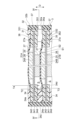
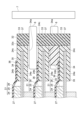
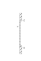
- FIG. 1 is a schematic cross-sectional view of a power storage device according to a first embodiment.
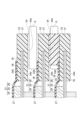
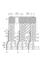
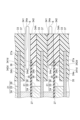
- FIG. 2 is a partially enlarged view of FIG. 1.
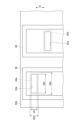
- FIG. 3 is a side view of the power storage device shown in FIG. 1.
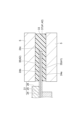
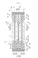
- FIG. 4 is a sectional view taken along line IV-IV in FIG. 2.
- FIG. 5 is a diagram showing steps of a method for manufacturing the power storage device shown in FIG. 1.
- FIG. 6 is a diagram showing steps of a method for manufacturing the power storage device shown in FIG. 1.
- FIG. 7 is a diagram showing steps of a method for manufacturing the power storage device shown in FIG. 1.
- FIG. 8 is a diagram showing steps of a method for manufacturing the power storage device shown in FIG. 1.
- FIG. 1 is a schematic cross-sectional view of a power storage device according to a first embodiment.
- FIG. 2 is a partially enlarged view of FIG. 1.
- FIG. 3 is a side view of the power storage device shown in FIG. 1.
- FIG. 4
- FIG. 9 is a diagram showing steps of a method for manufacturing the power storage device shown in FIG. 1.
- FIG. 10 is a diagram showing steps of a method for manufacturing the power storage device shown in FIG. 1.
- FIG. 11 is a diagram showing steps of a method for manufacturing the power storage device shown in FIG. 1.
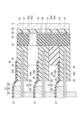
- FIG. 12 is a partially enlarged cross-sectional view of the power storage device according to the second embodiment.
- FIG. 13 is a diagram showing steps of a method for manufacturing the power storage device shown in FIG. 12.
- FIG. 14 is a diagram showing steps of a method for manufacturing the power storage device shown in FIG. 12.
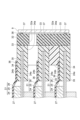
- FIG. 15 is a partially enlarged sectional view of a power storage device according to a third embodiment.
- FIG. 16 is a diagram showing steps of a method for manufacturing the power storage device shown in FIG. 15.
- FIG. 17 is a diagram showing steps of a method for manufacturing the power storage device shown in FIG. 15.
- a power storage device 1 according to the first embodiment shown in FIG. 1 is, for example, a power storage module used in a battery of a forklift, a hybrid vehicle, an electric vehicle, or the like.
- the power storage device 1 is, for example, a secondary battery such as a nickel-metal hydride secondary battery or a lithium ion secondary battery.
- power storage device 1 is a lithium ion secondary battery.
- power storage device 1 includes a laminate 2 and a sealing body 3.
- the laminate 2 includes a plurality of bipolar electrodes 21 , a positive terminal electrode 22 , and a negative terminal electrode 23 .
- the plurality of bipolar electrodes 21, positive terminal electrode 22, and negative terminal electrode 23 are stacked in the stacking direction D.
- Bipolar electrode 21 includes a current collector 24 , a positive electrode active material layer 25 , and a negative electrode active material layer 26 .
- the current collector 24 has, for example, a rectangular shape when viewed from the stacking direction D.
- Current collector 24 includes a surface 24a and a surface 24b opposite to surface 24a.
- the positive electrode active material layer 25 is provided on the surface 24a.
- the positive electrode active material layer 25 has, for example, a rectangular shape when viewed from the stacking direction D.
- the surface 24a includes an uncoated area where the positive electrode active material layer 25 is not provided.
- the uncoated area of the surface 24a surrounds the positive electrode active material layer 25 when viewed from the stacking direction D.
- the negative electrode active material layer 26 is provided on the surface 24b.
- the negative electrode active material layer 26 has, for example, a rectangular shape when viewed from the stacking direction D.
- the surface 24b includes an uncoated area where the negative electrode active material layer 26 is not provided.
- the uncoated area of the surface 24b surrounds the negative electrode active material layer 26 when viewed from the stacking direction D.
- the plurality of bipolar electrodes 21 are stacked such that the positive electrode active material layer 25 of one bipolar electrode 21 and the negative electrode active material layer 26 of the other bipolar electrode 21 face each other. That is, the plurality of bipolar electrodes 21 are arranged such that the surface 24a of the current collector 24 of one of the adjacent bipolar electrodes 21 and the surface 24b of the current collector 24 of the other bipolar electrode 21 face each other. are laminated on.
- the positive terminal electrode 22 is arranged on one side of the plurality of bipolar electrodes 21 in the stacking direction D.
- the positive terminal electrode 22 includes a current collector 24 and a positive active material layer 25 .
- the positive terminal electrode 22 differs from the bipolar electrode 21 in that it does not have the negative active material layer 26.
- the other configuration of the positive terminal electrode 22 may be the same as that of the bipolar electrode 21.
- the positive terminal electrode 22 is arranged such that the positive active material layer 25 of the positive terminal electrode 22 faces the negative active material layer 26 of the bipolar electrode 21 . That is, the positive terminal electrode 22 is stacked such that the surface 24a of the current collector 24 of the positive terminal electrode 22 and the surface 24b of the current collector 24 of the bipolar electrode 21 adjacent to the positive terminal electrode 22 face each other. .
- the negative terminal electrode 23 is arranged on the other side of the plurality of bipolar electrodes 21 in the stacking direction D.
- the negative terminal electrode 23 includes a current collector 24 and a negative active material layer 26 .
- the negative terminal electrode 23 differs from the bipolar electrode 21 in that it does not have the positive active material layer 25.
- the other configuration of the negative terminal electrode 23 may be the same as that of the bipolar electrode 21.
- the negative terminal electrode 23 is arranged such that the negative active material layer 26 of the negative terminal electrode 23 faces the positive active material layer 25 of the bipolar electrode 21 . That is, the negative terminal electrode 23 is stacked such that the surface 24b of the current collector 24 of the negative terminal electrode 23 and the surface 24a of the current collector 24 of the bipolar electrode 21 adjacent to the negative terminal electrode 23 face each other. .
- An internal space S containing an electrolytic solution is formed between each bipolar electrode 21, between the bipolar electrode 21 and the positive terminal electrode 22, and between the bipolar electrode 21 and the negative terminal electrode 23.
- the laminate 2 includes a plurality of separators 27.
- the separator 27 is arranged between each bipolar electrode 21 , between the bipolar electrode 21 and the positive terminal electrode 22 , and between the bipolar electrode 21 and the negative terminal electrode 23 .
- the separator 27 is located between the positive electrode active material layer 25 and the negative electrode active material layer 26 that face each other.
- the separator 27 has a sheet shape, for example.
- the separator 27 has, for example, a rectangular shape when viewed from the stacking direction D. When viewed from the stacking direction D, the outer edge of the separator 27 is located on the outer side of each of the outer edges of the positive electrode active material layer 25 and the outer edge of the negative electrode active material layer 26.
- the separator 27 is a member that allows charge carriers such as lithium ions to pass through. Separator 27 isolates adjacent electrodes 21, 22, and 23 from each other. This prevents electrical short circuits due to contact between the electrodes 21, 22, and 23.
- the current collector 24 is a chemically inert electrical conductor that allows current to continue flowing through the positive electrode active material layer 25 and the negative electrode active material layer 26 during discharging or charging of the lithium ion secondary battery.
- the material of the current collector 24 is, for example, a metal material, a conductive resin material, a conductive inorganic material, or the like.
- the conductive resin material include resins in which a conductive filler is added to a conductive polymer material or a non-conductive polymer material.
- the current collector 24 may include one or more layers containing the above-mentioned metal material or conductive resin material.
- a coating layer may be formed on the surface of the current collector 24 by a known method such as plating or spray coating.
- the current collector 24 may have a plate shape, a foil shape, a sheet shape, a film shape, a mesh shape, or the like, for example.
- the current collector 24 may be, for example, aluminum foil, copper foil, nickel foil, titanium foil, or stainless steel foil.
- the current collector 24 may be an alloy foil or clad foil of the above metal.
- the thickness of the current collector 24 may be in the range of 1 ⁇ m or more and 100 ⁇ m or less.
- the current collector 24 may be a laminate having a plurality of metal layers stacked in the stacking direction D.
- the current collector 24 may be a laminate in which an aluminum layer and a copper layer are integrated by, for example, plating one side of an aluminum foil with copper.
- the current collector 24 may be a laminate formed by bonding a plurality of metal foils together via a conductive adhesive.
- the current collector 24 has a first layer 241 and a second layer 242 stacked in the stacking direction D, and the first layer 241 and the second layer 242 are electrically connected. ing.
- the surface 24a of the current collector 24 is the surface of the first layer 241.
- the surface 24b of the current collector 24 is the surface of the second layer 242.
- the first layer 241 of the current collector 24 contains aluminum, and is, for example, aluminum foil.
- the second layer 242 of the current collector 24 contains copper, and is, for example, a copper foil. Note that the current collector 24 of the positive terminal electrode 22 does not need to have the second layer 242.
- the positive electrode active material layer 25 includes a positive electrode active material that can insert and release charge carriers such as lithium ions.
- the positive electrode active material include composite oxides, metallic lithium, and sulfur.
- the composition of the composite oxide includes, for example, at least one of iron, manganese, titanium, nickel, cobalt, and aluminum and lithium.
- the composite oxide include olivine-type lithium iron phosphate (LiFePO 4 ), LiCoO 2 , LiNiMnCoO 2 , and the like.
- the negative electrode active material layer 26 includes a negative electrode active material that can insert and release charge carriers such as lithium ions.
- negative electrode active materials include graphite, artificial graphite, highly oriented graphite, mesocarbon microbeads, carbon such as hard carbon and soft carbon, metal compounds, elements that can be alloyed with lithium or their compounds, boron-added carbon, etc. Can be mentioned.
- elements that can be alloyed with lithium include silicon and tin.
- Each of the positive electrode active material layer 25 and the negative electrode active material layer 26 may contain a binder and a conductive aid in addition to the active material.
- the binder plays the role of binding the active materials or conductive aids to each other and maintaining the conductive network in the electrode.
- fluororesins such as polyvinylidene fluoride, polytetrafluoroethylene, and fluororubber, thermoplastic resins such as polypropylene and polyethylene, imide resins such as polyimide and polyamideimide, alkoxysilyl group-containing resins, and polyacrylics are used.
- the conductive aid is a conductive material such as acetylene black, carbon black, graphite, etc., and can improve electrical conductivity.
- N-methyl-2-pyrrolidone or the like is used as the viscosity adjusting solvent.
- an active material layer-forming composition is prepared in the form of a slurry by mixing an active material, a solvent, and, if necessary, a binder and a conductive aid. After coating on 24a or surface 24b, it is dried.
- Solvents are, for example, N-methyl-2-pyrrolidone, methanol, methyl isobutyl ketone, water. In order to increase the electrode density, the dried material may be compressed.
- the separator 27 is, for example, a porous sheet or nonwoven fabric containing a polymer that absorbs and retains the electrolyte.
- the material of the separator 27 is, for example, polypropylene, polyethylene, polyolefin, polyester, or the like.
- the separator 27 may have a single layer structure or a multilayer structure.
- the separator 27 includes, for example, a base material layer and a pair of adhesive layers, and may be adhesively fixed to the positive electrode active material layer 25 and the negative electrode active material layer 26 by the pair of adhesive layers.
- Separator 27 may include a ceramic layer serving as a heat-resistant layer.
- the separator 27 may be reinforced with a vinylidene fluoride resin compound.
- Examples of the electrolytic solution impregnated into the separator 27 include a liquid containing a non-aqueous solvent and an electrolyte salt dissolved in the non-aqueous solvent.
- the electrolyte salt of the electrolytic solution known lithium salts such as LiClO 4 , LiAsF 6 , LiPF 6 , LiBF 4 , LiCF 3 SO 3 , LiN(FSO 2 ) 2 , LiN(CF 3 SO 2 ) 2 and the like can be used.
- the nonaqueous solvent known solvents such as cyclic carbonates, cyclic esters, chain carbonates, chain esters, and ethers can be used. Note that two or more of these known solvent materials may be used in combination.
- the sealing body 3 is a member that seals the internal space S.
- the sealing body 3 is provided on the side surface of the laminate 2 .
- the sealing body 3 seals the side surface of the laminate 2 .
- the sealing body 3 has a rectangular cylindrical shape, for example.
- the sealing body 3 has electrical insulation properties.
- the sealing body 3 has a main body portion 31 and a welded portion 32.
- the main body portion 31 is provided at the outer edge of the laminate 2 .
- the main body portion 31 is composed of a plurality of independent members.
- the main body part 31 has a plurality of seal parts 33 and a plurality of spacers 34.
- the seal portion 33 includes a seal portion 35 provided on the surface 24a of the current collector 24, a seal portion 36 provided on the surface 24b of the current collector 24, and a seal portion 37 provided on the side surface of the current collector 24. It has .
- Each seal portion 35, 36 has a rectangular frame shape, for example, when viewed from the stacking direction.
- the seal portion 35 surrounds the positive electrode active material layer 25 and the negative electrode active material layer 26 when viewed from the stacking direction D.
- An inner edge 35d of the seal portion 35 is separated from the positive electrode active material layer 25.
- the outer edge 35c of the seal portion 35 substantially coincides with the outer edge 24c of the current collector 24 when viewed from the stacking direction D.
- Seal portion 35 is welded to surface 24a.
- the seal portion 36 surrounds the positive electrode active material layer 25 and the negative electrode active material layer 26 when viewed from the stacking direction D.
- An inner edge 36d of the seal portion 36 is separated from the negative electrode active material layer 26.
- the inner edge 36d of the seal portion 36 substantially coincides with the inner edge 35d of the seal portion 35 when viewed from the stacking direction D.
- the outer edge 36c of the seal portion 36 substantially coincides with the outer edge 24c of the current collector 24 when viewed from the stacking direction D. Seal portion 36 is welded to surface 24b.
- the seal portion 37 is provided on the side surface of the current collector 24.
- the seal portion 37 covers the side surface of the current collector 24.
- the seal portion 37 is welded to the side surface of the current collector 24.
- the seal portion 37 seals between the first layer 241 and the second layer 242.
- the seal portion 37 is connected to an outer edge 35c of the seal portion 35 and an outer edge 36c of the seal portion 36, respectively.
- the seal portions 35, 36, and 37 are part of the seal portion 33 integrally formed of the same material.
- the spacer 34 has, for example, a rectangular frame shape (see FIG. 4) with a portion cut out for a liquid injection port 34a to be described later.
- the spacer 34 is provided between a pair of adjacent seal portions 33 in the stacking direction D.
- the inner edge 34d of the spacer 34 is located on the opposite side of the positive electrode active material layer 25 or the negative electrode active material layer 26 with respect to the inner edge 35d of the seal portion 35 and the inner edge 36d of the seal portion 36, respectively, when viewed from the stacking direction. You may do so. That is, the inner edge 34d of the spacer 34 may be located further away from the positive electrode active material layer 25 or the negative electrode active material layer 26 than the inner edge 35d of the seal portion 35 and the inner edge 36d of the seal portion 36.
- the outer edge 34c of the spacer 34 substantially coincides with the outer edge 33c of the seal portion 33 when viewed from the stacking direction D.
- the inner edge 34d of the spacer 34 may be located closer to the positive electrode active material layer 25 or the negative electrode active material layer 26 than the inner edge 35d of the seal portion 35 and the inner edge 36d of the seal portion 36.
- each of the seal portion 33 and the spacer 34 is, for example, acid-modified polyethylene (acid-modified PE), acid-modified polypropylene (acid-modified PP), polyethylene, or polypropylene.
- Each of the seal portion 33 and the spacer 34 has electrolyte resistance.
- the materials of the seal portion 33 and the spacer 34 may be the same or different.
- the material of the seal portion 33 is, for example, acid-modified polyethylene or acid-modified polypropylene.
- the material of the spacer 34 is, for example, polyethylene or polypropylene.
- Acid-modified polyethylene and acid-modified polypropylene are easier to bond to metals than non-acid-modified polyethylene and non-acid-modified polypropylene.
- the bonding strength of the seal portions 35, 36 to the current collector 24 can be improved by forming the seal portions 35, 36 from acid-modified polyethylene or acid-modified polypropylene.
- the welded part 32 is provided on the outside of the main body part 31.
- the welded portion 32 is integrated by welding the outer edges of each seal portion 33 and each spacer 34 .
- the welded portion 32 has, for example, a rectangular cylindrical shape.
- the welded portion 32 extends continuously in the stacking direction D from one end of the stacked body 2 to the other end.
- each seal portion 33 and each A welded portion 32 is formed by welding the outer edges of each of the spacers 34.
- the welded portion 32 may be formed such that the inner edge of the welded portion 32 does not overlap each current collector 24 when viewed from the stacking direction D.
- power storage device 1 includes a first electrode 21A and a second electrode 21B adjacent to the first electrode 21A.
- the first electrode 21A and the second electrode 21B are a pair of mutually adjacent bipolar electrodes 21 shown in FIG.
- the first electrode 21A has a first current collector 24A
- the second electrode 21B has a second current collector 24B.
- Each of the first current collector 24A and the second current collector 24B is the current collector 24 shown in FIG.
- Each of the first current collector 24A and the second current collector 24B includes a first surface 24d and a second surface 24e.
- the first surface 24d is the surface 24a shown in FIG. 1, and the second surface 24e is the surface 24b shown in FIG.
- the main body portion 31 has a first seal portion 331 and a second seal portion 332.
- the first seal portion 331 is provided on the first current collector 24A
- the second seal portion 332 is provided on the second current collector 24B.
- Each of the first seal portion 331 and the second seal portion 332 is the seal portion 33 shown in FIG.
- the first seal portion 331 includes a first seal portion 351.
- the first seal portion 351 is welded to the first surface 24d of the first current collector 24A.
- the first seal portion 351 is the seal portion 35 shown in FIG.
- the second seal portion 332 includes a second seal portion 362.
- the second seal portion 362 is welded to the second surface 24e of the second current collector 24B.
- Second seal portion 362 is seal portion 36 shown in FIG.
- the spacer 34 together with the first electrode 21A, the first seal portion 331, the second electrode 21B, and the second seal portion 332, forms an internal space S for accommodating the electrolyte.
- the spacer 34 is sandwiched between a first seal portion 351 and a second seal portion 362.
- the spacer 34 is a separate member from the first seal part 331 and the second seal part 332.
- the spacer 34 is in contact with each of the first seal portion 351 and the second seal portion 362.
- the spacer 34 is not welded to each of the first seal portion 351 and the second seal portion 362.
- the thickness T1 of the spacer 34 is larger than the thickness T2 of the first seal portion 351 and the thickness T3 of the second seal portion 362, respectively.
- the thickness T1 of the spacer 34 is, for example, twice or more the thickness T2 of the first seal portion 351 or the thickness T3 of the second seal portion 362.
- the thickness T1 of the spacer 34 is smaller than the thickness T4 of the first seal portion 331 or the second seal portion 332. That is, the thickness T1 of the spacer 34 is smaller than the sum of the thickness of the current collector 24, the thickness T2 of the first seal portion 351, and the thickness T3 of the second seal portion 362. Note that the thickness T2 of the first seal portion 351 and the thickness T3 of the second seal portion 362 may be the same or different.
- the peripheral edge 27a of the separator 27 is located between the spacer 34 and the second seal portion 362.
- the peripheral edge 27a of the separator 27 may be sandwiched between the spacer 34 and the second seal portion 362 in a region excluding a liquid injection port 34a, which will be described later.
- the peripheral edge portion 27a of the separator 27 may be welded and fixed to the second seal portion 362.
- the separator 27 divides the internal space S into a first region S1 and a second region S2.
- the first region S1 is a region in the internal space S between the separator 27 and the first electrode 21A.
- the second region S2 is a region of the internal space S between the separator 27 and the second electrode 21B.
- the volume of the first region S1 is larger than the volume of the second region S2.
- the area of the positive electrode active material layer 25 is smaller than the area of the negative electrode active material layer 26.
- the outer edge of the positive electrode active material layer 25 is located inside the outer edge of the negative electrode active material layer 26.
- a plurality of grooves 25a are formed in the positive electrode active material layer 25.
- the peripheral edge 27a of the separator 27 is located between the spacer 34 and the second seal portion 362.
- the volume of the first region S1 is larger than the volume of the second region S2.
- the thickness of the positive electrode active material layer 25 may be greater than the thickness of the negative electrode active material layer 26. In this case, the volume of the first region S1 becomes even larger than the volume of the second region S2.
- the spacer 34 includes a liquid injection port (first liquid injection port) 34a.
- the liquid injection port 34a penetrates the spacer 34.
- the liquid injection port 34a opens at each of the outer edge 34c and the inner edge 34d of the spacer 34.
- the liquid injection port 34a communicates with the internal space S.
- the liquid injection port 34a functions as a path for injecting the electrolyte into the internal space S.
- the liquid injection ports 34a of the plurality of spacers 34 may be formed at different positions when viewed from the stacking direction D. As an example, the liquid injection ports 34a of the plurality of spacers 34 lined up in the stacking direction D are arranged diagonally with respect to the stacking direction D.
- the respective liquid injection ports 34a communicating with the internal spaces S adjacent to each other in the stacking direction D are arranged at shifted positions so as not to overlap each other when viewed from the stacking direction D.
- the liquid injection port 34a has, for example, a rectangular shape when viewed from a direction intersecting the outer surface 32b of the welded portion 32.
- the welded part 32 includes a plurality of liquid injection ports (second liquid injection ports) 32a.
- the liquid injection port 32a penetrates the welded portion 32.
- the liquid injection port 32a opens on the outer surface 32b of the welded portion 32.
- the liquid inlet 32a communicates with the liquid inlet 34a.
- the liquid injection port 32a functions as a path for injecting the electrolyte into the internal space S via the liquid injection port 34a.
- Each liquid injection port 32a is arranged diagonally with respect to the stacking direction D, similarly to the liquid injection port 34a.
- the respective liquid injection ports 32a communicating with the internal spaces S adjacent to each other in the stacking direction D are arranged at shifted positions so as not to overlap each other when viewed from the stacking direction D.
- the liquid injection port 32a has, for example, a rectangular shape when viewed from a direction intersecting the outer surface 32b of the welded portion 32.
- the area of the liquid inlet 32a is smaller than the area of the liquid inlet 34a.
- the liquid inlet 32a may be located inside the liquid inlet 34a, for example.
- the width W1 of the liquid injection port 32a in the stacking direction D is smaller than the width W2 of the liquid injection port 34a in the stacking direction D.
- the width W3 of the liquid inlet 32a in the direction intersecting the stacking direction D is smaller than the width W4 of the liquid inlet 34a in the direction intersecting the stacking direction D.
- a frame portion 38 surrounding the liquid injection port 32a is formed on the outer surface 32b.
- the frame portion 38 protrudes from the outer surface 32b.
- the frame portion 38 has a rectangular frame shape, for example, when viewed from a direction intersecting the outer surface 32b.
- the inner edge of the frame portion 38 is located on the outer side of the liquid inlet 32a and the liquid inlet 34a.
- the inner region of the frame portion 38 communicates with the liquid injection port 34a via the liquid injection port 32a.
- the positive electrode active material layer 25 includes a plurality of grooves 25a.
- Each groove 25a extends in the direction in which the liquid inlet 32a, the liquid inlet 34a, and the internal space S are lined up.
- Each groove 25a reaches both ends of the positive electrode active material layer 25 in the extending direction of the groove 25a.
- the depth of each groove 25a in the stacking direction D is the same as the thickness of the positive electrode active material layer 25 in the stacking direction D. That is, each groove 25a is formed in the stacking direction D to reach the first surface 24d of the first current collector 24A.
- the first surface 24d of the first current collector 24A is exposed in each groove 25a.
- Each groove 25a is a part of the first region S1.
- the electrolytic solution injected from the liquid injection ports 32a and 34a can move through the region between the positive electrode active material layer 25 and the spacer 34 and each groove 25a in the first region S1.
- the bipolar electrode 21, the seal member 41, and the seal member 42 are prepared. Subsequently, the seal member 41 is placed on the surface 24a of the current collector 24, and the seal member 42 is placed on the surface 24b of the current collector 24.
- the sealing member 41 and the sealing member 42 are arranged so as to protrude from the outer edge 24c of the current collector 24, respectively. That is, when viewed from the stacking direction D, the sealing member 41 disposed on the surface 24a of the current collector 24 and the sealing member 42 disposed on the surface 24b of the current collector 24 are connected to the current collector 24, respectively. It has an overlapping portion and a portion that does not overlap with the current collector 24.
- each of the sealing member 41 and the sealing member 42 are heated by the heater 5.
- the heater 5 is, for example, an impulse sealer. Heating of the sealing member 41 and the sealing member 42 is performed with the heater 5 sandwiching the current collector 24 via the sealing member 41 and the sealing member 42, respectively. As a result, a portion of the seal member 41 that overlaps with the surface 24a is welded to the surface 24a, thereby forming a seal portion 35, and a portion of the seal member 42 that overlaps with the surface 24b is welded to the surface 24b. A seal portion 36 is thereby formed.
- seal portion 33 is formed on the bipolar electrode 21.
- a seal portion 33 is also formed on the positive terminal electrode 22 and the negative terminal electrode 23 by a similar process.
- each electrode 21, 22, 23 with a seal portion 33 formed thereon and each spacer 34 are stacked.
- a spacer 34 is arranged between each seal portion 33 .
- the liquid injection port forming member 6 is inserted into the liquid injection port 34a of the spacer 34.
- the liquid injection port forming member 6 has a plate shape, for example.
- the liquid injection port forming member 6 extends from the outside of the spacer 34 to the internal space S.
- the width of the liquid injection port forming member 6 is smaller than the width of the liquid injection port 34a. That is, a clearance exists between the liquid injection port forming member 6 and the liquid injection port 34a.
- the heating device 7 is, for example, an infrared heater.
- the heating device 7 irradiates the outer surfaces of each seal portion 33 and each spacer 34 with infrared rays.
- the temperature of each seal portion 33 and each spacer 34 increases.
- the heating of each seal portion 33 and each spacer 34 is controlled by the heating device 7 so that the temperature thereof is equal to or higher than the melting point. As a result, the outer edges of each seal portion 33 and each spacer 34 are melted.
- each seal portion 33 and each spacer 34 When the outer edges of each seal portion 33 and each spacer 34 are melted, the melted liquid portion flows to fill the gap between the liquid injection port 34a and the liquid injection port forming member 6. When heating by the heating device 7 is stopped, the melted outer edges of each seal portion 33 and each spacer 34 cool and solidify to become a welded portion 32.
- each liquid injection port forming member 6 is pulled out from the liquid injection port 34a.
- a liquid injection port 32a is formed in the welded portion 32.
- the frame portion 38 is formed on the outer surface 32b of the welded portion 32 by, for example, injection molding.
- the electrolytic solution is injected into each internal space S through each liquid injection port 32a and each liquid injection port 34a.
- the equipment side nozzle 8 is pressed against the frame portion 38.
- the equipment side nozzle 8 has a support member 81 and a seal member 82.
- the seal member 82 is provided on the surface of the support member 81.
- the seal member 82 is, for example, an elastic body.
- the seal member 82 is, for example, a packing.
- a plurality of liquid injection ports 8a are formed in the equipment side nozzle 8. Each liquid injection port 8a corresponds to each liquid injection port 32a and each liquid injection port 34a. The surface of the seal member 82 is pressed against the frame portion 38.
- the seal member 82 When the surface of the seal member 82 is pressed against the frame portion 38, at least a portion of the frame portion 38 bites into the seal member 82. Thereby, the space between the frame portion 38 and the seal member 82 is sealed. Subsequently, the electrolytic solution is injected into the internal space S using the equipment side nozzle 8.
- each liquid injection port 32a is sealed. Specifically, by joining the sealing material 9 to the frame 38, the liquid injection port 32a surrounded by the frame 38 is sealed. Thereby, power storage device 1 shown in FIG. 1 is manufactured. Note that in FIG. 1, illustration of the frame portion 38 and the sealing material 9 is omitted.
- the first seal portion 351 is welded to the first surface 24d of the first current collector 24A, and the second seal portion 351 is welded to the second surface 24e of the second current collector 24B. 362 is welded. Furthermore, the welded portion 32 is formed by welding the outer edges of each seal portion 33 and each spacer 34 . Thereby, the internal space S can be reliably sealed. Further, the thickness T1 of the spacer 34 is larger than each of the thickness T2 of the first seal portion 351 and the thickness T3 of the second seal portion 362, and the liquid injection port 34a is formed in the spacer 34. .
- the sealing body 3 that defines the internal space S together with the electrodes disposed opposite to each other a sufficient thickness in the stacking direction D of the spacer 34 for forming the liquid injection port 34a is ensured, and the first set of The thickness in the stacking direction D of the first seal portion 351 welded to the electric body 24A or the second seal portion 362 welded to the second current collector 24B can be made sufficiently small. Therefore, according to the power storage device 1, the deformation (for example, wrinkles, etc.) of the first current collector 24A due to welding of the first seal portion 351 to the first surface 24d, or the deformation of the second seal portion to the second surface 24e.
- the width in the stacking direction D of the liquid injection port 34a, which serves as a flow path when injecting the electrolyte, can be increased, and the electrolyte can be efficiently injected into the internal space S. Can be done.
- the width of the liquid inlet 32a is smaller than the width of the liquid inlet 34a. Thereby, backflow of the electrolytic solution accommodated in the internal space S to the outside can be suppressed.
- the peripheral edge 27a of the separator 27 is fixed to the seal portion 36.
- the volume of the first region S1 of the interior space S is larger than the volume of the second region S2 of the interior space S.
- the area of the positive electrode active material layer 25 is smaller than the area of the negative electrode active material layer 26.
- the volume of the first region S1 can be made larger than the volume of the second region S2, and as described above, smooth liquid injection can be realized.
- the thickness of the positive electrode active material layer 25 is greater than the thickness of the negative electrode active material layer 26. Thereby, the volume of the first region S1 can be made larger than the volume of the second region S2, and as described above, smooth liquid injection can be realized.
- the positive electrode active material layer 25 includes a groove 25a extending in the direction in which the liquid injection port 34a and the internal space S are lined up. This prevents the flow of the electrolytic solution from being obstructed by the positive electrode active material layer 25, so that smooth injection can be achieved. In addition, since the grooves 25a reach the surface 24a of the current collector 24, gases generated during the formation of the positive electrode active material layer 25 on the surface 24a are efficiently removed from between the surface 24a and the positive electrode active material layer 25. It can be discharged well.
- the current collector 24 has a first layer 241 and a second layer 242.
- the seal portion 33 includes a seal portion 35 welded to the surface 24a, a seal portion 36 welded to the surface 24b, and a seal portion 37 welded to the side surface of the current collector 24.
- the seal length between the first layer 241 and the seal portion 33 is ensured, so that the electrolyte is distributed between the seal portion 35 and the surface 24a of the first layer 241 and between the seal portion 37 and the side surface of the first layer 241. It is possible to prevent the second layer 242 from coming into contact with the second layer 242 after entering between the two layers.
- the electrolyte is allowed to flow between the seal portion 36 and the surface 24b of the second layer 242 and between the seal portion 37 and the side surface of the second layer 242. It is possible to prevent the first layer 241 from coming into contact with the first layer 241 after entering between the two layers.
- the power storage device of the second embodiment mainly differs from the power storage device 1 of the first embodiment in that it includes a spacer 34A instead of the spacer 34.
- the spacer 34A is provided between the first seal part 331 and the second seal part 332.
- the spacer 34A includes a first spacer 341 and a second spacer 342. Each of the first spacer 341 and the second spacer 342 is a separate member.
- the first spacer 341 has, for example, a rectangular frame shape with a portion cut out for a liquid injection port 34a to be described later.
- the first spacer 341 is in contact with the first seal portion 351 of the first seal portion 331 .
- the first spacer 341 is not welded to the first seal portion 351.
- the inner edge 341d of the first spacer 341 is located on the opposite side of the positive electrode active material layer 25 with respect to the inner edge 35d of the first seal portion 351 when viewed from the stacking direction D. That is, the inner edge 341d of the first spacer 341 is located further away from the positive electrode active material layer 25 than the inner edge 35d of the first seal portion 351.
- the first spacer 341 includes a liquid injection port (first liquid injection port) 34a. That is, the liquid injection port 34a is formed in the first spacer 341.
- the liquid injection port 34a penetrates the first spacer 341.
- the liquid injection port 34a opens at each of the outer edge and inner edge 341d
- the second spacer 342 has a rectangular frame shape, for example.
- the second spacer 342 is provided between the first spacer 341 and the second seal portion 332.
- the second spacer 342 is in contact with the first spacer 341.
- the second spacer 342 is in contact with the second seal portion 362 of the second seal portion 332 .
- the second spacer 342 is not welded to the second seal portion 362.
- the inner edge 342d of the second spacer 342 is located on the opposite side of the negative electrode active material layer 26 with respect to the inner edge 36d of the second seal portion 362 when viewed from the stacking direction D. That is, the inner edge 342d of the second spacer 342 is located further away from the negative electrode active material layer 26 than the inner edge 36d of the second seal portion 362.
- the inner edge 342d of the second spacer 342 substantially coincides with the inner edge 341d of the first spacer 341 when viewed from the stacking direction D.
- the second spacer 342 does not include a liquid injection port.
- the second spacer 342 has a frame shape that is continuously connected in the circumferential direction.
- the thickness T11 of the first spacer 341 is larger than the thickness T2 of the first seal portion 351 and the thickness T3 of the second seal portion 362, respectively.
- the thickness T12 of the second spacer 342 is larger than the thickness T2 of the first seal portion 351 and the thickness T3 of the second seal portion 362, respectively.
- the thickness T11 of the first spacer 341 and the thickness T12 of the second spacer 342 are the same. That is, each of the thickness T11 of the first spacer 341 and the thickness T12 of the second spacer 342 is about half the thickness T1 of the spacer 34A.
- the thickness T11 of the first spacer 341 and the thickness T12 of the second spacer 342 may be different.
- the thickness T11 of the first spacer 341 may be greater than the thickness T12 of the second spacer 342.
- the thickness T11 of the first spacer 341 may be smaller than the thickness T12 of the second spacer 342.
- the thickness T11 of the first spacer 341 may be less than or equal to the thickness T2 of the first seal portion 351 or the thickness T3 of the second seal portion 362.
- the thickness T12 of the second spacer 342 may be less than or equal to the thickness T2 of the first seal portion 351 or the thickness T3 of the second seal portion 362.
- the peripheral edge 27a of the separator 27 is located between the first spacer 341 and the second spacer 342.
- the peripheral edge 27a of the separator 27 is welded to the second spacer 342.
- the peripheral edge 27a of the separator 27 is welded to the surface of the second spacer 342 that faces the first spacer 341.
- the peripheral edge 27a of the separator 27 is welded to the second spacer 342 over the entire circumference of the second spacer 342. That is, the portion of the separator 27 that is welded to the second spacer 342 has a rectangular frame shape when viewed from the stacking direction D.
- seal portions 33 are formed on each electrode 21, 22, 23 (see FIGS. 5 and 6).
- the peripheral edge 27a of the separator 27 is welded to the second spacer 342. Specifically, after the peripheral edge 27a of the separator 27 is placed on one side of the second spacer 342, the peripheral edge 27a of the separator 27 and the second spacer 342 are heated.
- the electrodes 21, 22, 23 on which the seal portion 33 is formed, the second spacer 342 and the first spacer 341 on which the separator 27 is welded are stacked.
- the first spacer 341 is arranged on one side of the second spacer 342 to which the peripheral edge 27a of the separator 27 is welded.
- the first spacer 341 and the second spacer 342 are arranged between each seal portion 33.
- the liquid injection port forming member 6 is inserted into the liquid injection port 34a.
- formation of a welded portion, injection of an electrolytic solution, sealing of a liquid injection port, etc. are performed. In this way, the power storage device of the second embodiment is manufactured.
- the spacer 34A includes a first spacer 341 and a second spacer 342, each of which is formed into a frame shape and stacked in the stacking direction D. This makes it easy to adjust the thickness of spacer 34A, making it easy to manufacture the power storage device. Further, since the spacer 34A includes a plurality of spacers, the thickness of each spacer 341, 342 is smaller than the distance between adjacent seal parts 33, and as a result, it is thinner than when a single spacer is used. can do. This makes it easier to wind the precursors of the spacers 341 and 342 into a roll, for example. Therefore, the precursors of the spacers 341 and 342 can be easily handled, and as a result, the power storage device can be manufactured easily.
- the peripheral edge 27a of the separator 27 is welded to the second spacer 342.
- the separator 27 is not welded to the first spacer 341 in the region of the first spacer 341 where the liquid injection port 34a is formed. Fixation may be insufficient.
- the peripheral edge 27a of the separator 27 is welded to the second spacer 342 in which the liquid injection port 34a is not formed. can be fixed to. Therefore, short circuit between each electrode 21, 22, 23 can be suppressed.
- the separator 27 When the separator 27 is welded to the first seal portion 351 or the second seal portion 362, after welding the first seal portion 351 or the second seal portion 362 to the current collector 24, the separator 27 is welded to the first seal portion 351 or the second seal portion 362. It may be welded to the portion 351 or the second seal portion 362. In such a case, since the first seal portion 351 or the second seal portion 362 is heated multiple times, the welding strength of the first seal portion 351 or the second seal portion 362 to the current collector 24 is reduced. There is a risk of it getting lost.
- the peripheral edge 27a of the separator 27 is welded to the second spacer 342, so that the first seal portion 351 or the second seal portion 362 is connected to the current collector 24. Decrease in welding strength is suppressed.
- the power storage device of the third embodiment differs from the power storage device of the second embodiment mainly in that it includes a spacer 34B instead of spacer 34A. As shown in FIG. 15, the spacer 34B is provided between the first seal part 331 and the second seal part 332.
- the spacer 34B includes a first spacer 341, a second spacer 342, and a third spacer 343. Each of the first spacer 341, second spacer 342, and third spacer 343 is a separate member.
- the thickness T11 of the first spacer 341 is approximately 1 ⁇ 3 of the thickness T1 of the spacer 34B.
- the other points of the first spacer 341 are the same as the first spacer 341 of the second embodiment.
- the second spacer 342 is provided between the first spacer 341 and the third spacer 343.
- the thickness T12 of the second spacer 342 is the same as the thickness T11 of the first spacer 341. That is, the thickness T12 of the second spacer 342 is about 1 ⁇ 3 of the thickness T1 of the spacer 34B.
- the inner edge 342d of the second spacer 342 is located inside the inner edge 341d of the first spacer 341 when viewed from the stacking direction D.
- the inner edge 342d of the second spacer 342 is located inside the inner edge 35d of the first seal portion 351 or the inner edge 36d of the second seal portion 362 when viewed from the stacking direction D.
- the width of the side portion of the second spacer 342 is greater than the width of the side portion of the first spacer 341.
- the other points of the second spacer 342 are the same as the second spacer 342 of the second embodiment.
- the third spacer 343 is stacked on the side opposite to the first spacer 341 with respect to the second spacer 342.
- the third spacer 343 has a rectangular frame shape, for example.
- the thickness T13 of the third spacer 343 is the same as the thickness T11 of the first spacer 341. That is, the thickness T13 of the third spacer 343 is about 1 ⁇ 3 of the thickness T1 of the spacer 34B.
- the third spacer 343 is in contact with the second seal portion 362 of the second seal portion 332 .
- the third spacer 343 is not welded to the second seal portion 362.
- the inner edge 343d of the third spacer 343 is located on the opposite side of the negative electrode active material layer 26 with respect to the inner edge 36d of the second seal portion 362 when viewed from the stacking direction D.
- the inner edge 343d of the third spacer 343 substantially coincides with the inner edge 341d of the first spacer 341 when viewed from the stacking direction D.
- the third spacer 343 includes a liquid injection port (first liquid injection port) 34a. That is, the liquid injection port 34a is also formed in the third spacer 343. The liquid injection port 34a passes through the third spacer 343. The liquid injection port 34a opens at each of the outer edge and inner edge 343d of the third spacer 343.
- the thickness T11 of the first spacer 341, the thickness T12 of the second spacer 342, and the thickness T13 of the third spacer 343 are each different from the thickness T2 of the first seal portion 351 and the thickness T3 of the second seal portion 362. greater than each.
- the thickness T11 of the first spacer 341, the thickness T12 of the second spacer 342, and the thickness T13 of the third spacer 343 may be different from each other similarly to the power storage device of the second embodiment.
- the thickness T13 of the third spacer 343 may be less than or equal to the thickness T2 of the first seal portion 351 or the thickness T3 of the second seal portion 362.
- the peripheral edge 27a of the separator 27 is welded to the second spacer 342.
- the peripheral edge 27a of the separator 27 is welded to the surface of the second spacer 342 that faces the first spacer 341.
- the peripheral edge 27a of the separator 27 is welded to a portion of the second spacer 342 that is inside the first spacer 341.
- the peripheral edge 27a of the separator 27 is welded to the second spacer 342 over the entire circumference of the second spacer 342. That is, the portion of the separator 27 that is welded to the second spacer 342 has a rectangular frame shape when viewed from the stacking direction D. Note that the peripheral edge portion 27a of the separator 27 may extend between the first spacer 341 and the second spacer 342.
- seal portions 33 are formed on each electrode 21, 22, 23 (see FIGS. 5 and 6).
- the peripheral edge 27a of the separator 27 is welded to the second spacer 342. Specifically, after the peripheral edge 27a of the separator 27 is placed on one side of the second spacer 342, the peripheral edge 27a of the separator 27 and the second spacer 342 are heated.
- the electrodes 21, 22, 23 on which the seal portion 33 is formed, the second spacer 342 on which the separator 27 is welded, the first spacer 341, and the third spacer 343 are stacked.
- the first spacer 341 is arranged on one side of the second spacer 342 to which the peripheral edge 27a of the separator 27 is welded.
- the third spacer 343 is arranged on the opposite side of the first spacer 341 with respect to the second spacer 342 .
- the first spacer 341 , the second spacer 342 , and the third spacer 343 are arranged between each seal portion 33 .
- the liquid injection port forming member 6 is inserted into the liquid injection port 34a.
- formation of a welded portion, injection of an electrolytic solution, sealing of a liquid injection port, etc. are performed. In this way, the power storage device of the third embodiment is manufactured.
- the inner edge 342d of the second spacer 342 is located inside the inner edge 341d of the first spacer 341. Thereby, a sufficient area of the second spacer 342 for welding the separator 27 can be secured. Therefore, the peripheral edge 27a of the separator 27 can be fixed more reliably, and short circuits between the electrodes 21, 22, 23 can be more reliably suppressed.
- the spacer 34B includes a third spacer 343 stacked on the opposite side of the first spacer 341 to the second spacer 342.
- the liquid injection port 34a is formed in each of the first spacer 341 and the third spacer 343. Thereby, liquid can be injected from both sides of the separator 27 in the stacking direction D. Therefore, smooth liquid injection can be achieved.
- the first electrode 21A is the positive terminal electrode 22
- the second electrode 21B is the bipolar electrode 21 adjacent to the positive terminal electrode 22.
- attention may be paid to the negative terminal electrode 23 and the bipolar electrode 21 adjacent to the negative terminal electrode 23.
- the first electrode 21A is the bipolar electrode 21 adjacent to the negative terminal electrode 23, and the second electrode 21B is the negative terminal electrode 23.
- the current collector 24 has the first layer 241 and the second layer 242, but the current collector 24 may have only one layer.
- the peripheral edge 27a of the separator 27 is welded to the surface of the second spacer 342 that faces the first spacer 341, but the peripheral edge 27a of the separator 27 is , may be welded to the surface of the second spacer 342 opposite to the first spacer 341.
- an example was shown in which the peripheral edge part 27a of the separator 27 is welded to the second spacer 342 over the entire circumference of the second spacer 342, but the peripheral edge part of the separator 27 27a may be welded to the second spacer 342 at predetermined intervals in the circumferential direction of the second spacer 342.
- the peripheral edge 27a of the separator 27 may be partially welded to the second spacer 342. Even in this case, the separator 27 can be welded to the second spacer 342 at intervals independent of the width of the liquid injection port 34a, so the peripheral edge 27a of the separator 27 can be reliably fixed. Note that in the second embodiment and the third embodiment, the separator 27 does not need to be welded to the spacers 34A, 34B. In the second embodiment and the third embodiment, the peripheral edge 27a of the separator 27 may be welded to the first seal portion 351 or the second seal portion 362. In the second embodiment and the third embodiment, the separator 27 does not need to be welded.
- the gist of the present disclosure is as follows [1] to [10].
- a laminate including a first electrode and a second electrode laminated in a stacking direction, and a sealing body for sealing a side surface of the laminate, wherein the first electrode has a first surface. and a positive electrode active material layer provided on the first surface, and the second electrode has a second current collector including a second surface opposite to the first surface. and a negative electrode active material layer provided on the second surface, and the sealing body is welded to the first surface so as to surround the positive electrode active material layer when viewed from the stacking direction.
- a first seal portion including a first seal portion; a second seal portion including a second seal portion welded to the second surface so as to surround the negative electrode active material layer when viewed from the stacking direction; a spacer sandwiched between the first seal portion and the second seal portion; and the spacer located outside the respective outer edges of the first current collector and the second current collector when viewed from the stacking direction.
- a welded part formed by welding outer edges of each of the first seal part, the second seal part, and the spacer, and the spacer includes the first electrode, the second electrode, and the sealing body.
- the welded portion includes a first liquid inlet that is formed by the spacer and communicates with an internal space in which an electrolytic solution is accommodated, and the welded part includes a second liquid inlet that communicates with the first liquid inlet, and the welded part includes a second liquid inlet that communicates with the first liquid inlet, and
- the power storage device has a thickness larger than each of the first seal portion and the second seal portion.
- the power storage device according to [7] Further comprising a separator provided between the positive electrode active material layer and the negative electrode active material layer, the first liquid injection port is formed in the first spacer, and the peripheral edge of the separator is , the power storage device according to [7], which is welded to the second spacer.
- the spacer further includes a third spacer stacked on a side opposite to the first spacer with respect to the second spacer, and the first liquid inlet is connected to the first spacer and the third spacer.
- SYMBOLS 1 Power storage device, 2... Laminated body, 3... Sealing body, 21... Bipolar electrode, 24... Current collector, 24a, 24b... Surface, 25... Positive electrode active material layer, 25a... Groove, 26... Negative electrode active material layer , 27... Separator, 27a... Peripheral part, 32... Welding part, 34... Spacer, 32a, 34a... Liquid inlet, 33... Seal part, 35, 36... Seal part, 341... First spacer, 342... Second spacer , 343...Third spacer, S...Internal space, S1...First region, S2...Second region.
Landscapes
- Chemical & Material Sciences (AREA)
- Chemical Kinetics & Catalysis (AREA)
- Electrochemistry (AREA)
- General Chemical & Material Sciences (AREA)
- Engineering & Computer Science (AREA)
- Manufacturing & Machinery (AREA)
- Power Engineering (AREA)
- Materials Engineering (AREA)
- Microelectronics & Electronic Packaging (AREA)
- Condensed Matter Physics & Semiconductors (AREA)
- General Physics & Mathematics (AREA)
- Inorganic Chemistry (AREA)
- Physics & Mathematics (AREA)
- Secondary Cells (AREA)
Abstract
Description
図1に示される第1実施形態に係る蓄電装置1は、例えば、フォークリフト、ハイブリッド自動車、又は電気自動車等のバッテリに用いられる蓄電モジュールである。蓄電装置1は、例えばニッケル水素二次電池又はリチウムイオン二次電池等のような二次電池である。本実施形態では、蓄電装置1は、リチウムイオン二次電池である。
第2実施形態の蓄電装置は、スペーサ34に代えてスペーサ34Aを備えている点で、第1実施形態の蓄電装置1と主に異なる。図12に示されるように、スペーサ34Aは、第1シール部331と第2シール部332との間に設けられている。スペーサ34Aは、第1スペーサ341及び第2スペーサ342を含んでいる。第1スペーサ341及び第2スペーサ342のそれぞれは、別部材である。
第3実施形態の蓄電装置は、スペーサ34Aに代えてスペーサ34Bを備えている点で、第2実施形態の蓄電装置と主に異なる。図15に示されるように、スペーサ34Bは、第1シール部331と第2シール部332との間に設けられている。スペーサ34Bは、第1スペーサ341、第2スペーサ342及び第3スペーサ343を含んでいる。第1スペーサ341、第2スペーサ342及び第3スペーサ343のそれぞれは、別部材である。
[1]積層方向に積層された第1電極及び第2電極を含む積層体と、前記積層体の側面を封止するための封止体と、を備え、前記第1電極は、第1表面を含む第1集電体と、前記第1表面に設けられた正極活物質層と、を有し、前記第2電極は、前記第1表面に対向する第2表面を含む第2集電体と、前記第2表面に設けられた負極活物質層と、を有し、前記封止体は、前記積層方向から見た場合に前記正極活物質層を囲むように前記第1表面に溶着された第1シール部分を含む第1シール部と、前記積層方向から見た場合に前記負極活物質層を囲むように前記第2表面に溶着された第2シール部分を含む第2シール部と、前記第1シール部分及び前記第2シール部分によって挟まれたスペーサと、前記積層方向から見た場合に前記第1集電体及び前記第2集電体のそれぞれの外縁よりも外側に位置する前記第1シール部、前記第2シール部及び前記スペーサのそれぞれの外縁部の溶着によって形成された溶着部と、を有し、前記スペーサは、前記第1電極、前記第2電極及び前記封止体によって形成されると共に電解液が収容される内部空間に連通する第1注液口を含み、前記溶着部は、前記第1注液口に連通する第2注液口を含み、前記スペーサの厚さは、前記第1シール部分及び前記第2シール部分のそれぞれの厚さよりも大きい、蓄電装置。
[2]前記第2注液口の幅は、前記第1注液口の幅よりも小さい、[1]に記載の蓄電装置。
[3]前記正極活物質層と前記負極活物質層との間に設けられたセパレータを更に備え、前記セパレータの周縁部は、前記スペーサと前記第2シール部分との間に位置し、前記内部空間のうち、前記セパレータと前記第1電極との間の第1領域の容積は、前記セパレータと前記第2電極との間の第2領域の容積よりも大きい、[1]又は[2]に記載の蓄電装置。
[4]前記積層方向から見た場合に、前記正極活物質層の面積は、前記負極活物質層の面積よりも小さい、[3]に記載の蓄電装置。
[5]前記正極活物質層の厚さは、前記負極活物質層の厚さよりも大きい、[3]又は[4]に記載の蓄電装置。
[6]前記正極活物質層は、前記第1注液口と前記内部空間とが並ぶ方向において延在する溝を含んでいる、[1]~[5]のいずれか一項に記載の蓄電装置。
[7]前記スペーサは、それぞれが枠状に形成され、前記積層方向に積層された第1スペーサ及び第2スペーサを含んでいる、[1]に記載の蓄電装置。
[8]前記正極活物質層と前記負極活物質層との間に設けられたセパレータを更に備え、前記第1注液口は、前記第1スペーサに形成されており、前記セパレータの周縁部は、前記第2スペーサに溶着されている、[7]に記載の蓄電装置。
[9]前記積層方向から見た場合に、前記第2スペーサの内縁は、前記第1スペーサの内縁よりも内側に位置している、[8]に記載の蓄電装置。
[10]前記スペーサは、前記第2スペーサに対して前記第1スペーサとは反対側に積層された第3スペーサを更に含み、前記第1注液口は、前記第1スペーサ及び前記第3スペーサのそれぞれに形成されている、[7]~[9]のいずれか一項に記載の蓄電装置。
Claims (10)
- 積層方向に積層された第1電極及び第2電極を含む積層体と、
前記積層体の側面を封止するための封止体と、を備え、
前記第1電極は、第1表面を含む第1集電体と、前記第1表面に設けられた正極活物質層と、を有し、
前記第2電極は、前記第1表面に対向する第2表面を含む第2集電体と、前記第2表面に設けられた負極活物質層と、を有し、
前記封止体は、前記積層方向から見た場合に前記正極活物質層を囲むように前記第1表面に溶着された第1シール部分を含む第1シール部と、
前記積層方向から見た場合に前記負極活物質層を囲むように前記第2表面に溶着された第2シール部分を含む第2シール部と、
前記第1シール部分及び前記第2シール部分によって挟まれたスペーサと、
前記積層方向から見た場合に前記第1集電体及び前記第2集電体のそれぞれの外縁よりも外側に位置する前記第1シール部、前記第2シール部及び前記スペーサのそれぞれの外縁部の溶着によって形成された溶着部と、を有し、
前記スペーサは、前記第1電極、前記第2電極及び前記封止体によって形成されると共に電解液が収容される内部空間に連通する第1注液口を含み、
前記溶着部は、前記第1注液口に連通する第2注液口を含み、
前記スペーサの厚さは、前記第1シール部分及び前記第2シール部分のそれぞれの厚さよりも大きい、蓄電装置。 - 前記第2注液口の幅は、前記第1注液口の幅よりも小さい、請求項1に記載の蓄電装置。
- 前記正極活物質層と前記負極活物質層との間に設けられたセパレータを更に備え、
前記セパレータの周縁部は、前記スペーサと前記第2シール部分との間に位置し、
前記内部空間のうち、前記セパレータと前記第1電極との間の第1領域の容積は、前記セパレータと前記第2電極との間の第2領域の容積よりも大きい、請求項1又は2に記載の蓄電装置。 - 前記積層方向から見た場合に、前記正極活物質層の面積は、前記負極活物質層の面積よりも小さい、請求項3に記載の蓄電装置。
- 前記正極活物質層の厚さは、前記負極活物質層の厚さよりも大きい、請求項3に記載の蓄電装置。
- 前記正極活物質層は、前記第1注液口と前記内部空間とが並ぶ方向において延在する溝を含んでいる、請求項1に記載の蓄電装置。
- 前記スペーサは、それぞれが枠状に形成され、前記積層方向に積層された第1スペーサ及び第2スペーサを含んでいる、請求項1に記載の蓄電装置。
- 前記正極活物質層と前記負極活物質層との間に設けられたセパレータを更に備え、
前記第1注液口は、前記第1スペーサに形成されており、
前記セパレータの周縁部は、前記第2スペーサに溶着されている、請求項7に記載の蓄電装置。 - 前記積層方向から見た場合に、前記第2スペーサの内縁は、前記第1スペーサの内縁よりも内側に位置している、請求項8に記載の蓄電装置。
- 前記スペーサは、前記第2スペーサに対して前記第1スペーサとは反対側に積層された第3スペーサを更に含み、
前記第1注液口は、前記第1スペーサ及び前記第3スペーサのそれぞれに形成されている、請求項8に記載の蓄電装置。
Priority Applications (4)
| Application Number | Priority Date | Filing Date | Title |
|---|---|---|---|
| KR1020247024881A KR102841786B1 (ko) | 2022-03-29 | 2023-03-01 | 축전 장치 |
| CN202380031005.8A CN118974988A (zh) | 2022-03-29 | 2023-03-01 | 蓄电装置 |
| EP23779179.3A EP4439751A4 (en) | 2022-03-29 | 2023-03-01 | ENERGY STORAGE DEVICE |
| US18/834,529 US20250132397A1 (en) | 2022-03-29 | 2023-03-01 | Power storage device |
Applications Claiming Priority (4)
| Application Number | Priority Date | Filing Date | Title |
|---|---|---|---|
| JP2022-053493 | 2022-03-29 | ||
| JP2022053493 | 2022-03-29 | ||
| JP2022-094629 | 2022-06-10 | ||
| JP2022094629A JP7779204B2 (ja) | 2022-03-29 | 2022-06-10 | 蓄電装置 |
Publications (1)
| Publication Number | Publication Date |
|---|---|
| WO2023189149A1 true WO2023189149A1 (ja) | 2023-10-05 |
Family
ID=88201112
Family Applications (1)
| Application Number | Title | Priority Date | Filing Date |
|---|---|---|---|
| PCT/JP2023/007634 Ceased WO2023189149A1 (ja) | 2022-03-29 | 2023-03-01 | 蓄電装置 |
Country Status (4)
| Country | Link |
|---|---|
| US (1) | US20250132397A1 (ja) |
| EP (1) | EP4439751A4 (ja) |
| KR (1) | KR102841786B1 (ja) |
| WO (1) | WO2023189149A1 (ja) |
Families Citing this family (1)
| Publication number | Priority date | Publication date | Assignee | Title |
|---|---|---|---|---|
| US20250201984A1 (en) * | 2022-04-08 | 2025-06-19 | Kabushiki Kaisha Toyota Jidoshokki | Power storage device |
Citations (4)
| Publication number | Priority date | Publication date | Assignee | Title |
|---|---|---|---|---|
| JP2018120718A (ja) * | 2017-01-24 | 2018-08-02 | 株式会社豊田自動織機 | 蓄電モジュールの製造方法 |
| JP2019129070A (ja) * | 2018-01-24 | 2019-08-01 | 株式会社豊田自動織機 | バイポーラ電池の製造方法及びバイポーラ電池 |
| JP2019200955A (ja) | 2018-05-18 | 2019-11-21 | 株式会社豊田自動織機 | 蓄電モジュールの製造方法 |
| JP2021015699A (ja) * | 2019-07-11 | 2021-02-12 | 株式会社豊田自動織機 | 蓄電モジュール |
Family Cites Families (5)
| Publication number | Priority date | Publication date | Assignee | Title |
|---|---|---|---|---|
| JP2006318662A (ja) * | 2005-05-10 | 2006-11-24 | Ngk Spark Plug Co Ltd | 薄型電池およびその製造方法 |
| JP7059837B2 (ja) * | 2018-07-06 | 2022-04-26 | 株式会社豊田自動織機 | 蓄電モジュールの製造方法及び供給装置 |
| JP2020071951A (ja) * | 2018-10-30 | 2020-05-07 | 株式会社豊田自動織機 | 蓄電モジュール及び蓄電モジュールの製造方法 |
| JP7103272B2 (ja) * | 2019-02-28 | 2022-07-20 | 株式会社豊田自動織機 | 蓄電モジュール及びその製造方法 |
| JP2021140971A (ja) * | 2020-03-06 | 2021-09-16 | 株式会社豊田自動織機 | 蓄電セル、及び、蓄電セルの製造方法 |
-
2023
- 2023-03-01 US US18/834,529 patent/US20250132397A1/en active Pending
- 2023-03-01 EP EP23779179.3A patent/EP4439751A4/en active Pending
- 2023-03-01 WO PCT/JP2023/007634 patent/WO2023189149A1/ja not_active Ceased
- 2023-03-01 KR KR1020247024881A patent/KR102841786B1/ko active Active
Patent Citations (4)
| Publication number | Priority date | Publication date | Assignee | Title |
|---|---|---|---|---|
| JP2018120718A (ja) * | 2017-01-24 | 2018-08-02 | 株式会社豊田自動織機 | 蓄電モジュールの製造方法 |
| JP2019129070A (ja) * | 2018-01-24 | 2019-08-01 | 株式会社豊田自動織機 | バイポーラ電池の製造方法及びバイポーラ電池 |
| JP2019200955A (ja) | 2018-05-18 | 2019-11-21 | 株式会社豊田自動織機 | 蓄電モジュールの製造方法 |
| JP2021015699A (ja) * | 2019-07-11 | 2021-02-12 | 株式会社豊田自動織機 | 蓄電モジュール |
Non-Patent Citations (1)
| Title |
|---|
| See also references of EP4439751A4 |
Also Published As
| Publication number | Publication date |
|---|---|
| EP4439751A4 (en) | 2025-09-03 |
| KR20240128944A (ko) | 2024-08-27 |
| EP4439751A1 (en) | 2024-10-02 |
| KR102841786B1 (ko) | 2025-08-04 |
| US20250132397A1 (en) | 2025-04-24 |
Similar Documents
| Publication | Publication Date | Title |
|---|---|---|
| JP2024037418A (ja) | 蓄電装置及び蓄電装置の製造方法 | |
| JP7779204B2 (ja) | 蓄電装置 | |
| JP7559840B2 (ja) | 蓄電セル及び蓄電装置 | |
| JP2021096910A (ja) | 蓄電装置の製造方法及び蓄電装置 | |
| KR102841786B1 (ko) | 축전 장치 | |
| US20250105458A1 (en) | Power storage device | |
| WO2024062824A1 (ja) | 蓄電モジュール及び蓄電装置 | |
| CN114747061B (zh) | 蓄电装置和蓄电装置的制造方法 | |
| WO2023120171A1 (ja) | 蓄電装置 | |
| JP7750402B2 (ja) | 蓄電装置 | |
| JP2022077634A (ja) | 蓄電装置 | |
| CN118974988A (zh) | 蓄电装置 | |
| JP2021082532A (ja) | 蓄電セルの製造方法 | |
| JP2025097647A (ja) | 蓄電モジュールの製造方法及び蓄電モジュールの製造装置 | |
| JP2025179995A (ja) | 蓄電モジュール製造方法 | |
| JP2025037409A (ja) | バイポーラ電池の製造方法 | |
| WO2025249117A1 (ja) | 蓄電モジュール | |
| JP2021082534A (ja) | 蓄電セルの製造方法及び蓄電セル | |
| JP2024162813A (ja) | 蓄電モジュール | |
| JP2025002705A (ja) | 蓄電装置 | |
| JP2024113307A (ja) | 蓄電装置の製造方法 | |
| WO2024053312A1 (ja) | 蓄電装置 | |
| JP2025072870A (ja) | バイポーラ電池の製造方法 | |
| JP2021082533A (ja) | 蓄電セルの製造方法 | |
| JP2022086271A (ja) | 蓄電装置 |
Legal Events
| Date | Code | Title | Description |
|---|---|---|---|
| 121 | Ep: the epo has been informed by wipo that ep was designated in this application |
Ref document number: 23779179 Country of ref document: EP Kind code of ref document: A1 |
|
| WWE | Wipo information: entry into national phase |
Ref document number: 2023779179 Country of ref document: EP |
|
| ENP | Entry into the national phase |
Ref document number: 2023779179 Country of ref document: EP Effective date: 20240626 |
|
| ENP | Entry into the national phase |
Ref document number: 20247024881 Country of ref document: KR Kind code of ref document: A |
|
| WWE | Wipo information: entry into national phase |
Ref document number: 18834529 Country of ref document: US |
|
| WWE | Wipo information: entry into national phase |
Ref document number: 202417066270 Country of ref document: IN |
|
| WWE | Wipo information: entry into national phase |
Ref document number: 202380031005.8 Country of ref document: CN |
|
| NENP | Non-entry into the national phase |
Ref country code: DE |
|
| WWP | Wipo information: published in national office |
Ref document number: 18834529 Country of ref document: US |