WO2023195236A1 - パッケージおよびパッケージの製造方法 - Google Patents
パッケージおよびパッケージの製造方法 Download PDFInfo
- Publication number
- WO2023195236A1 WO2023195236A1 PCT/JP2023/004705 JP2023004705W WO2023195236A1 WO 2023195236 A1 WO2023195236 A1 WO 2023195236A1 JP 2023004705 W JP2023004705 W JP 2023004705W WO 2023195236 A1 WO2023195236 A1 WO 2023195236A1
- Authority
- WO
- WIPO (PCT)
- Prior art keywords
- chip
- dummy
- optical
- substrate
- molding material
- Prior art date
- Legal status (The legal status is an assumption and is not a legal conclusion. Google has not performed a legal analysis and makes no representation as to the accuracy of the status listed.)
- Ceased
Links
Images


Classifications
-
- H—ELECTRICITY
- H10—SEMICONDUCTOR DEVICES; ELECTRIC SOLID-STATE DEVICES NOT OTHERWISE PROVIDED FOR
- H10F—INORGANIC SEMICONDUCTOR DEVICES SENSITIVE TO INFRARED RADIATION, LIGHT, ELECTROMAGNETIC RADIATION OF SHORTER WAVELENGTH OR CORPUSCULAR RADIATION
- H10F39/00—Integrated devices, or assemblies of multiple devices, comprising at least one element covered by group H10F30/00, e.g. radiation detectors comprising photodiode arrays
- H10F39/80—Constructional details of image sensors
- H10F39/804—Containers or encapsulations
-
- H—ELECTRICITY
- H10—SEMICONDUCTOR DEVICES; ELECTRIC SOLID-STATE DEVICES NOT OTHERWISE PROVIDED FOR
- H10W—GENERIC PACKAGES, INTERCONNECTIONS, CONNECTORS OR OTHER CONSTRUCTIONAL DETAILS OF DEVICES COVERED BY CLASS H10
- H10W90/00—Package configurations
-
- H—ELECTRICITY
- H10—SEMICONDUCTOR DEVICES; ELECTRIC SOLID-STATE DEVICES NOT OTHERWISE PROVIDED FOR
- H10F—INORGANIC SEMICONDUCTOR DEVICES SENSITIVE TO INFRARED RADIATION, LIGHT, ELECTROMAGNETIC RADIATION OF SHORTER WAVELENGTH OR CORPUSCULAR RADIATION
- H10F39/00—Integrated devices, or assemblies of multiple devices, comprising at least one element covered by group H10F30/00, e.g. radiation detectors comprising photodiode arrays
- H10F39/011—Manufacture or treatment of image sensors covered by group H10F39/12
- H10F39/026—Wafer-level processing
-
- H—ELECTRICITY
- H10—SEMICONDUCTOR DEVICES; ELECTRIC SOLID-STATE DEVICES NOT OTHERWISE PROVIDED FOR
- H10F—INORGANIC SEMICONDUCTOR DEVICES SENSITIVE TO INFRARED RADIATION, LIGHT, ELECTROMAGNETIC RADIATION OF SHORTER WAVELENGTH OR CORPUSCULAR RADIATION
- H10F39/00—Integrated devices, or assemblies of multiple devices, comprising at least one element covered by group H10F30/00, e.g. radiation detectors comprising photodiode arrays
- H10F39/10—Integrated devices
- H10F39/12—Image sensors
- H10F39/199—Back-illuminated image sensors
-
- H—ELECTRICITY
- H10—SEMICONDUCTOR DEVICES; ELECTRIC SOLID-STATE DEVICES NOT OTHERWISE PROVIDED FOR
- H10F—INORGANIC SEMICONDUCTOR DEVICES SENSITIVE TO INFRARED RADIATION, LIGHT, ELECTROMAGNETIC RADIATION OF SHORTER WAVELENGTH OR CORPUSCULAR RADIATION
- H10F39/00—Integrated devices, or assemblies of multiple devices, comprising at least one element covered by group H10F30/00, e.g. radiation detectors comprising photodiode arrays
- H10F39/80—Constructional details of image sensors
- H10F39/811—Interconnections
-
- H—ELECTRICITY
- H10—SEMICONDUCTOR DEVICES; ELECTRIC SOLID-STATE DEVICES NOT OTHERWISE PROVIDED FOR
- H10W—GENERIC PACKAGES, INTERCONNECTIONS, CONNECTORS OR OTHER CONSTRUCTIONAL DETAILS OF DEVICES COVERED BY CLASS H10
- H10W70/00—Package substrates; Interposers; Redistribution layers [RDL]
- H10W70/60—Insulating or insulated package substrates; Interposers; Redistribution layers
- H10W70/611—Insulating or insulated package substrates; Interposers; Redistribution layers for connecting multiple chips together
-
- H—ELECTRICITY
- H10—SEMICONDUCTOR DEVICES; ELECTRIC SOLID-STATE DEVICES NOT OTHERWISE PROVIDED FOR
- H10W—GENERIC PACKAGES, INTERCONNECTIONS, CONNECTORS OR OTHER CONSTRUCTIONAL DETAILS OF DEVICES COVERED BY CLASS H10
- H10W70/00—Package substrates; Interposers; Redistribution layers [RDL]
- H10W70/60—Insulating or insulated package substrates; Interposers; Redistribution layers
- H10W70/62—Insulating or insulated package substrates; Interposers; Redistribution layers characterised by their interconnections
- H10W70/63—Vias, e.g. via plugs
- H10W70/635—Through-vias
-
- H—ELECTRICITY
- H10—SEMICONDUCTOR DEVICES; ELECTRIC SOLID-STATE DEVICES NOT OTHERWISE PROVIDED FOR
- H10W—GENERIC PACKAGES, INTERCONNECTIONS, CONNECTORS OR OTHER CONSTRUCTIONAL DETAILS OF DEVICES COVERED BY CLASS H10
- H10W70/00—Package substrates; Interposers; Redistribution layers [RDL]
- H10W70/60—Insulating or insulated package substrates; Interposers; Redistribution layers
- H10W70/62—Insulating or insulated package substrates; Interposers; Redistribution layers characterised by their interconnections
- H10W70/65—Shapes or dispositions of interconnections
-
- H—ELECTRICITY
- H10—SEMICONDUCTOR DEVICES; ELECTRIC SOLID-STATE DEVICES NOT OTHERWISE PROVIDED FOR
- H10W—GENERIC PACKAGES, INTERCONNECTIONS, CONNECTORS OR OTHER CONSTRUCTIONAL DETAILS OF DEVICES COVERED BY CLASS H10
- H10W72/00—Interconnections or connectors in packages
- H10W72/90—Bond pads, in general
-
- H—ELECTRICITY
- H10—SEMICONDUCTOR DEVICES; ELECTRIC SOLID-STATE DEVICES NOT OTHERWISE PROVIDED FOR
- H10W—GENERIC PACKAGES, INTERCONNECTIONS, CONNECTORS OR OTHER CONSTRUCTIONAL DETAILS OF DEVICES COVERED BY CLASS H10
- H10W74/00—Encapsulations, e.g. protective coatings
- H10W74/10—Encapsulations, e.g. protective coatings characterised by their shape or disposition
- H10W74/131—Encapsulations, e.g. protective coatings characterised by their shape or disposition the semiconductor body being only partially enclosed
- H10W74/141—Encapsulations, e.g. protective coatings characterised by their shape or disposition the semiconductor body being only partially enclosed the encapsulations being on at least the sidewalls of the semiconductor body
-
- H—ELECTRICITY
- H10—SEMICONDUCTOR DEVICES; ELECTRIC SOLID-STATE DEVICES NOT OTHERWISE PROVIDED FOR
- H10W—GENERIC PACKAGES, INTERCONNECTIONS, CONNECTORS OR OTHER CONSTRUCTIONAL DETAILS OF DEVICES COVERED BY CLASS H10
- H10W90/00—Package configurations
- H10W90/401—Package configurations characterised by multiple insulating or insulated package substrates, interposers or RDLs
Definitions
- the present technology relates to a package and a method for manufacturing the package. Specifically, the present technology relates to a package on which a chip is mounted and a method for manufacturing the package.
- a three-dimensional integrated structure in which solidified semiconductor chips are stacked is sometimes used in order to suppress an increase in the mounting area.
- a three-dimensional integrated structure for example, there is a structure in which a first chip and a second chip are mounted on an interposer substrate, and a third chip is stacked on the second chip (see, for example, Patent Document 1).
- This technology was created in view of this situation, and its purpose is to suppress the increase in package size while supporting expansion of functionality.
- the present technology was developed to solve the above-mentioned problems, and its first aspect is that it includes a plurality of chips including optical chips, a wiring layer on which the plurality of chips are mounted, and a wiring layer on which the plurality of chips are mounted.
- the package includes a molding material that is arranged to surround at least one of the chips and has a flattened surface. This brings about the effect that the optical chip with the transparent member provided above is sealed with the molding material.
- the heightwise position of the flat surface of the molding material is approximately equal to the heightwise position of the top surface of at least one of the plurality of chips. Good too. This brings about the effect that the surface of the transparent member is exposed from the molding material.
- the optical chip may include at least one of a light receiving element and a light emitting element. This brings about the effect that the optical chip functions as a light receiving element or a light emitting element.
- the wiring layer on which the plurality of chips are mounted may be a wiring layer formed on an interposer substrate or a rewiring layer formed on the chip. This brings about the effect that the optical chip is supported on the wiring layer.
- the first side surface may further include an antireflection film formed on at least one of the chips other than the optical chip and the mold material. This provides the effect of avoiding the influence of reflected light from around the optical chip.
- the first side surface may further include a lower chip on which at least one of the plurality of chips is mounted, and a through electrode formed in the lower chip. This brings about the effect that the mounting area of the chip is reduced.
- the first side surface is arranged at a distance around one of the plurality of chips in a state where the periphery is surrounded by the mold material, and has a height that is approximately the same as the flat surface of the mold material.
- the device may further include a dummy chip, the top surface of which is located at the top. This brings about the effect of improving the uniformity of the height of the mounting area where chips of different sizes are mounted.
- the first side further includes a transparent member provided above the optical chip, and the mold material is positioned so as to surround the optical chip with the surface of the transparent member exposed. You may. This brings about the effect that the optical chip with the transparent member provided above is sealed with the molding material.
- the transparent member may include at least one of a transparent resin and a transparent substrate. This brings about the effect that the upper part of the optical chip is sealed with the transparent member and the periphery of the optical chip is sealed with the molding material.
- the transparent member may include an optically functional layer. This brings about the effect of adding an optical function while sealing the periphery of the optical chip with the molding material.
- the top surface of the optical chip may be located at a lower position than the top surface of the mold material. This brings about the effect that the periphery of the optical chip is protected by the molding material.
- the first side surface may further include a transparent substrate or an optical member placed above the optical chip and supported by the dummy chip. This brings about the effect that the optical chip can be sealed or an optical function can be added without providing a transparent substrate or a supporting member for the optical member separately from the dummy chip.
- the top surface of the optical chip may be located at a higher position than the top surface of the mold material. This provides the effect of avoiding the effect of the molding material on the optical characteristics of the optical chip.
- the first side surface may further include an underfill provided between at least one chip of the plurality of chips and the wiring layer and around the chip. This brings about the effect of improving the sealing properties of the chip.
- At least a portion of the surfaces of the dummy chip, including the upper end of one surface facing the chip, is larger than the other surface facing the chip.
- the distance between the chip and the chip surrounded by the periphery may be large. This has the effect of enlarging the underfill inflow path between the dummy chip and the chip.
- At least one of the surfaces of the dummy chip facing the chip may have a forward tapered shape. This brings about the effect that the underfill can easily flow into the gap between the dummy chip and the chip.
- the second side surface includes an optical chip mounted on the substrate, a transparent member provided on the optical chip, and a surface flattened so that the surface of the transparent member is exposed, and the optical chip and a sealing resin formed on the substrate so as to surround the periphery of the substrate. This brings about the effect that the optical chip with the transparent member provided above is sealed with the sealing resin.
- the flattened surface may be a polished surface where polishing is stopped at the position of the transparent member. This brings about the effect that the optical function of the optical chip is ensured while sealing the optical chip provided above with the transparent member with the sealing resin.
- the third side surface includes a first chip on which a first wiring layer is formed, and extended rewiring that is electrically connected to the first wiring layer and that extends laterally from the mounting area of the first chip. and a second chip having a second wiring layer mounted on the extended redistribution layer and electrically connected to the extended redistribution layer, separated from the first chip. be. This brings about the effect that the second chip is mounted on the extended rewiring layer electrically connected to the first wiring layer of the first chip.
- the third side surface is formed on the extended rewiring layer so as to surround at least one of the first chip and the second chip, and has a flattened surface. It may further include. This brings about the effect that the chips on the extended redistribution layer on which a plurality of chips are mounted are sealed.
- the third side surface is placed on the expanded redistribution layer in a spaced apart manner around at least one of the first chip and the second chip, with the periphery surrounded by the molding material.
- the device may further include a dummy chip whose top surface is located at substantially the same height as the surface of the mold material. This brings about the effect of improving the uniformity of the height of the mounting area on the extended redistribution layer on which a plurality of chips of different sizes are mounted.
- a fourth side surface includes an optical chip mounted on the substrate, a dummy chip arranged on the substrate at a distance around the optical chip, and protruding from a top surface of the optical chip, and the optical chip. and a transparent member disposed above the dummy chip and supported by the dummy chip. This brings about the effect that the optical chip is sealed without providing a support member for the transparent substrate separately from the dummy chip.
- the fourth side surface may further include a molding material formed on the substrate so as to surround the dummy chip and having a flattened surface. This brings about the effect that the upper part of the optical chip is sealed with the transparent substrate and the periphery of the optical chip is sealed.
- the fifth aspect includes a step of sealing the optical chip with the transparent member provided above with a molding material together with a dummy substrate, and flattening the surface of the molding material so that the surfaces of the transparent member and the dummy substrate are sealed.
- a method of manufacturing a package includes the steps of exposing, removing at least a portion of the dummy substrate from which the surface is exposed, and mounting a chip in the region from which the dummy substrate has been removed. This brings about the effect that while the upper part of the optical chip is sealed with the transparent member, the periphery of the optical chip is sealed with the molding material, and the chip is later attached to a position surrounded by the dummy substrate.
- the flattening of the surface of the molding material may be stopped at the position of the transparent member. This brings about the effect that the optical function of the optical chip is ensured while sealing the optical chip with the transparent member provided above with the molding material.
- the sixth aspect includes a step of sealing the chip and the dummy substrate with a molding material, a step of flattening the surface of the molding material to expose the surface of the dummy substrate, and a step of sealing the chip and the dummy substrate with a molding material.
- This method of manufacturing a package includes a step of removing at least a portion of a dummy substrate, and a step of mounting an optical chip in a region from which the dummy substrate has been removed. This brings about the effect that the optical chip is later attached to a position surrounded by the dummy substrate while the periphery of the chip is sealed with the molding material.
- FIG. 3 is a diagram illustrating a configuration example of a package according to the first embodiment.
- FIG. 7 is a cross-sectional view showing an example of the configuration of a package according to a second embodiment.
- FIG. 7 is a plan view showing a configuration example of a package according to a second embodiment.
- FIG. 7 is a first cross-sectional view and a plan view showing an example of a method for manufacturing a package according to a second embodiment.
- FIG. 7 is a second cross-sectional view showing an example of a method for manufacturing a package according to a second embodiment.
- FIG. 7 is a third cross-sectional view showing an example of the method for manufacturing the package according to the second embodiment.
- FIG. 7 is a fourth cross-sectional view showing an example of the method for manufacturing a package according to the second embodiment.
- FIG. 7 is a fifth cross-sectional view showing an example of the method for manufacturing a package according to the second embodiment.
- FIG. 7 is a sixth cross-sectional view showing an example of the method for manufacturing a package according to the second embodiment.
- FIG. 7 is a seventh cross-sectional view showing an example of the method for manufacturing a package according to the second embodiment.
- FIG. 8 is an eighth cross-sectional view showing an example of the method for manufacturing a package according to the second embodiment.
- FIG. 9 is a ninth cross-sectional view showing an example of the method for manufacturing a package according to the second embodiment.
- FIG. 10 is a tenth cross-sectional view showing an example of the method for manufacturing a package according to the second embodiment.
- FIG. 11 is an eleventh cross-sectional view showing an example of the method for manufacturing a package according to the second embodiment.
- FIG. 7 is a cross-sectional view showing a configuration example of a package according to a third embodiment.
- FIG. 7 is a cross-sectional view showing a modified example of the structure of the package according to the third embodiment.
- FIG. 7 is a first cross-sectional view showing an example of a method for manufacturing a package according to a third embodiment.
- FIG. 7 is a second cross-sectional view showing an example of a method for manufacturing a package according to a third embodiment.
- FIG. 7 is a cross-sectional view showing a configuration example of a package according to a fourth embodiment.
- FIG. 7 is a cross-sectional view showing a configuration example of a package according to a fifth embodiment. It is a figure showing the example of composition of the package concerning a 6th embodiment.
- FIG. 7 is a cross-sectional view showing an example of the configuration of a package according to a seventh embodiment.
- FIG. 12 is a cross-sectional view showing an example of the configuration of a package according to an eightieth embodiment.
- FIG. 7 is a plan view showing an example of the configuration of a dummy chip of a package according to an eighth embodiment.
- FIG. 9 is a cross-sectional view showing an example of the configuration of a package according to a ninth embodiment.
- FIG. 7 is a cross-sectional view showing an example of the configuration of a package according to a tenth embodiment.
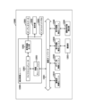
- FIG. 1 is a block diagram showing a schematic configuration example of a vehicle control system.
- FIG. 3 is an explanatory diagram showing an example of an installation position of an imaging unit.
- First embodiment an example in which an optical chip with a transparent member placed above and surrounded by a molding material with a flattened surface is mounted on an interposer substrate
- Second embodiment an example in which a semiconductor chip is retrofitted onto an interposer substrate on which an optical chip is mounted, which is surrounded by a molding material whose surface is flattened and a transparent member is placed above
- Third embodiment (example in which an optical functional layer is provided on a transparent member placed above an optical chip) 4.
- Fourth Embodiment Example in which a semiconductor chip is retrofitted on an extended redistribution layer on which an optical chip is mounted and a transparent member supported by a molding material is placed above.
- Fifth embodiment example in which an antireflection film is provided on the mold material and on the dummy chip.
- Sixth embodiment example in which a transparent member located above an optical chip is supported by a dummy chip.
- Seventh embodiment an example in which a transparent substrate positioned above an optical chip retrofitted to an interposer substrate mounted with a semiconductor chip surrounded by a molding material whose surface is flattened is supported by a dummy chip) ) 8.
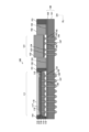
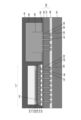
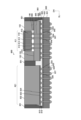
- FIG. 1 is a diagram showing an example of the configuration of a package according to the first embodiment. Note that a in the same figure is a cross-sectional view showing an example of the structure of the package according to the first embodiment, and b in the same figure is a plan view showing an example of the structure of the package according to the first embodiment. A in the same figure shows a sectional view taken along the line A1-A2 of b in the same figure.
- a package 100 includes an optical chip 111.
- Optical chip 111 is mounted on interposer substrate 130.
- the optical element is formed on the optical chip 111.
- the optical element may be a solid-state imaging device such as a CCD (Charged Coupled Device) or a CMOS (Complementary Metal-Oxide Semiconductor).
- the light received by the solid-state image sensor may be visible light, near infrared light (NIR), short wavelength infrared (SWIR), ultraviolet light, or X-rays.
- the optical element may be a light receiving element such as a PD (Photo Diode), or a light emitting element such as an LD (Laser Diode), an LED (Light Emitting Diode), or a VCSEL (Vertical Cavity Surface Emitting Laser).
- the optical element may be a MEMS (Micro Electro Mechanical Systems) element such as an optical switch or a mirror device.
- the material used for the base material of the optical chip 111 may be a semiconductor such as Si, GaAS, or InGaAsP, or may be a dielectric such as LiNbO 3 , glass, or transparent resin. Note that in the following description, a back-illuminated solid-state image sensor is taken as an example of the optical chip 111.
- the optical chip 111 includes a semiconductor layer 112 and a wiring layer 113.
- the semiconductor layer 112 is provided with an imaging region and a non-imaging region. In the imaging region, pixels and pixel transistors are arranged in a matrix along the row direction and the column direction. Peripheral circuits that drive pixel transistors and output signals read out from pixels are provided in the non-imaging area.
- an on-chip lens 116 is formed for each pixel.
- the material of the on-chip lens 116 for example, transparent resin such as acrylic or polycarbonate can be used.
- a color filter may be provided between the semiconductor layer 112 and the on-chip lens 116 for each pixel. At this time, the color filters can form a Bayer array, for example.
- a transparent resin 117 is formed on the back side of the semiconductor layer 112 so as to cover the on-chip lens 116 .
- a transparent substrate 118 is arranged on the transparent resin 117.
- the material of the transparent resin 117 is, for example, silicone, acrylic, or polycarbonate. At this time, the refractive index of the transparent resin 117 can be made smaller than the refractive index of the on-chip lens 116.
- the material of the transparent substrate 118 may be, for example, quartz, glass, or Al 2 O 3 , CaF 2 , MgF 2 , LiF, etc. depending on the wavelength of the optical element.
- the transparent resin 117 may be used as an adhesive for bonding the transparent substrate 118.
- the combined thickness of the transparent resin 117 and the transparent substrate 118 is preferably about 3 to 400 ⁇ m. Note that the transparent resin 117 and the transparent substrate 118 are examples of transparent members described in the claims.
- a wiring layer 113 is formed on the surface side of the semiconductor layer 112.
- the wiring layer 113 is provided with wiring embedded in an insulating layer. Furthermore, a pad electrode to which the through electrode 110 is connected can be formed in the wiring layer 113.
- the wiring layer 113 is supported by a support substrate 114.
- a land electrode 115 is formed on the support substrate 114, and a through electrode 110 is embedded in the support substrate 114.
- the wiring layer 113 is electrically connected to the land electrode 115 via the through electrode 110.
- the material of the insulating layer used for the wiring layer 113 for example, SiO 2 can be used.
- the material of the support substrate 114 for example, Si or glass can be used.
- the material of the wiring and pad electrode used in the wiring layer 113 can be, for example, a metal such as Al or Cu.
- metals such as Cu, Ti, Ta, Al, W, Ni, Ru, and Co can be used, and a laminated structure of a plurality of materials may be used.
- the interposer substrate 130 includes a support substrate 131 and a wiring layer 132.
- a semiconductor substrate such as Si, an organic substrate, or a ceramic substrate can be used.
- a land electrode 133 is formed on the wiring layer 132.
- Wiring (not shown) may be formed in the wiring layer 132.
- a land electrode 134 is formed on the back surface of the support substrate 131.
- Backside wiring may be formed on the backside of the support substrate 131.
- through electrodes 135 are formed in the support substrate 131 and the wiring layer 132. Land electrodes 133 and 134 are electrically connected to each other via a through electrode 135.
- the material of the through electrode 135 and the land electrodes 133 and 134 for example, metals such as Cu, Ti, Ta, Al, W, Ni, Ru, and Co can be used. Good too.
- the thickness of the interposer substrate 130 is preferably 30 to 300 ⁇ m.
- the land electrode 115 is connected to the land electrode 133 via a bump electrode 136.
- the bump electrode 136 may be a solder ball or a pillar electrode.
- an underfill 119 is provided between the interposer substrate 130 and the optical chip 111 and around the optical chip 111.
- the material of the underfill 119 is, for example, a thermosetting resin such as epoxy resin.
- a molding material 151 is arranged on the interposer substrate 130 so as to surround the optical chip 111. At this time, the molding material 151 can contact the side surface of the optical chip 111 and the side surface of the underfill 119. Furthermore, the position of the end of the molding material 151 in the lateral direction DL and the position of the end of the interposer substrate 130 in the lateral direction DL can coincide with each other. At this time, by cutting out the mold material 151 surrounding the optical chip 111 together with the interposer substrate 130, the package 100 can be made into a solid piece.
- the material of the mold material 151 may be thermosetting resin such as epoxy resin.
- the material of the mold material 151 may be a thermosetting resin mixed with silica filler.
- the surface of the molding material 151 is flattened at a position surrounding the optical chip 111.
- the flat surface of the mold material 151 may be a polished surface.
- the transparent substrate 118 can be used as a stopper for polishing the mold material 151.
- the position of the flat surface of the mold material 151 in the height direction DH can be made approximately equal to the position of the top surface of the optical chip 111 in the height direction DH. Note that the position of the flat surface of the molding material 151 in the height direction DH does not necessarily have to be strictly equal to the position of the top surface of the optical chip 111 in the height direction DH; It may be lower or higher than the DH position.
- the optical chip 111 with the transparent substrate 118 disposed above and surrounded by the molding material 151 whose surface is flattened is mounted on the interposer substrate 130. be done.
- Second embodiment> In the first embodiment described above, the optical chip 111 with the transparent substrate 118 disposed above is mounted on the interposer substrate 130 so as to be surrounded by the molding material 151 with a flattened surface.
- a semiconductor chip is later attached onto an interposer substrate 130 on which an optical chip 111 is mounted and a transparent substrate 118 is placed above so as to be surrounded by a molding material 151 whose surface is flattened.
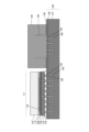
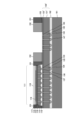
- FIG. 2 is a sectional view showing an example of the structure of a package according to the second embodiment
- FIG. 3 is a plan view showing an example of the structure of the package according to the second embodiment.
- FIG. 2 shows a cross-sectional view taken along line B1-B2 in FIG.
- a package 160 has a semiconductor chip 121 and a dummy chip 152 added to the package 100 of the first embodiment described above. Additionally, land electrodes 143 and 144 and a through electrode 145 are added to the interposer substrate 130.
- the other configuration of the package 160 of the second embodiment is similar to the configuration of the package 100 of the first embodiment described above.
- the optical chip 111 and the semiconductor chip 121 are mounted on an interposer substrate 130.
- the semiconductor chip 121 is an example of a chip described in the claims.
- a semiconductor element is formed on the semiconductor chip 121.
- Semiconductor elements may include transistors, resistors, capacitors, and the like.
- the semiconductor chip 121 may include a memory, a processor, a signal processing circuit, a data processing circuit, or an interface circuit. or an optical element may be formed.
- a hardware circuit such as an FPGA (Field-Programmable Gate Array) or an ASIC (Application Specific Integrated Circuit) may be formed on the semiconductor chip 121.
- the material used for the base material of the semiconductor chip 121 may be Si, GaAS, SiC, GaN, InGaAsP, or the like.
- the semiconductor chip 121 includes a semiconductor substrate 122 and a wiring layer 123.
- the wiring layer 123 is formed on the semiconductor substrate 122.
- the wiring layer 123 is provided with wiring embedded in an insulating layer. Further, a land electrode 124 to which a bump electrode 146 is connected can be formed on the wiring layer 123.
- land electrodes 143 are formed on the wiring layer 132 of the interposer substrate 130.
- a land electrode 144 is formed on the back surface of the support substrate 131.
- a through electrode 145 is formed in the support substrate 131 and the wiring layer 132. Land electrodes 143 and 144 are electrically connected to each other via a through electrode 145.
- metals such as Cu, Ti, Ta, Al, W, Ni, Ru, and Co can be used, and a laminated structure of a plurality of materials can also be used. good.
- the land electrode 124 is connected to the land electrode 143 via a bump electrode 146.
- the bump electrode 146 may be a solder ball or a pillar electrode.
- a dummy chip 152 is arranged on the interposer substrate 130 so as to surround the semiconductor chip 121.
- the dummy chip 152 can be placed on the interposer substrate 130 apart from the semiconductor chip 121.
- the dummy chip 152 can be fixed to the interposer substrate 130 via an adhesive 153.
- the surface of the dummy chip 152 is flattened.
- the position of the flat surface of the dummy chip 152 in the height direction DH can be made approximately equal to the position of the top surface of the optical chip 111 in the height direction DH.
- the position of the flat surface of the dummy chip 152 in the height direction DH does not necessarily have to be strictly equal to the position of the top surface of the optical chip 111 in the height direction DH; It may be lower or higher than the DH position.
- the material of the dummy chip 152 may be a semiconductor such as Si, or an inorganic material such as glass or ceramics.
- FIG. 3 shows an example in which the semiconductor chip 121 is placed in the center of the dummy chip 152, the dummy chip may be placed in an area including the front, rear, right, and left ends. Further, the dummy chip 152 may not be provided.
- the mold material 151 is placed on the interposer substrate 130 so as to surround the optical chip 111 and the dummy chip 152, respectively. At this time, the molding material 151 can contact the side surface of the optical chip 111, the side surface of the underfill 119, and the outer peripheral surface of the dummy chip 152. Furthermore, the position of the end of the molding material 151 in the lateral direction DL and the position of the end of the interposer substrate 130 in the lateral direction DL can coincide with each other.
- the surface of the molding material 151 is flattened at positions surrounding the optical chip 111 and the dummy chip 152, respectively.
- the flat surface of the mold material 151 may be a polished surface.
- the transparent substrate 118 can be used as a stopper for polishing the mold material 151.
- the position of the flat surface of the mold material 151 in the height direction DH can be made approximately equal to the position of the top surface of the optical chip 111 in the height direction DH.
- the top surface of the optical chip 111 is the surface of the transparent substrate 118.
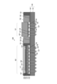
- FIG. 4 is a cross-sectional view and a plan view showing an example of a method for manufacturing a package according to the second embodiment
- FIGS. 5 to 14 are cross-sectional views showing an example of a method for manufacturing a package according to the second embodiment. It is a diagram. Note that b in FIG. 4 shows a cross-sectional view taken along the C1-C2 line of a in FIG. 4.
- a continuous rectangular groove 155 is formed in the dummy substrate 154.
- the groove 155 can be formed along the inner peripheral surface of the dummy chip 152.
- the dummy chip 152 can be separated from the dummy substrate 154 along the groove 155.
- the depth of the groove 155 is made greater than the height of the dummy chip 152.
- the depth of the groove 155 is approximately 20 to 400 ⁇ m.
- the material of the dummy substrate 154 may be a semiconductor such as Si, or an inorganic material such as glass or ceramics.
- the grooves 155 may be formed by using lithography and dry etching, or by laser processing or cutting. Note that when the dummy chip 152 is not provided in the package 160, the groove 155 is not necessary.
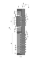
- an interposer wafer 130' is formed.
- a plurality of interposer substrates 130 used for the package 160 in FIG. 2 can be cut out from this interposer wafer 130'.
- embedded electrodes 135' and 145' are formed on the interposer wafer 130'.
- the thickness of the support substrate wafer 131' is made larger than the depth of the embedded electrodes 135' and 145'.
- the depth of the buried electrodes 135' and 145' is made equal to the length of the through electrodes 135 and 145.
- a wiring layer 132' having land electrodes 133 and 143 formed on its surface is formed on the support substrate wafer 131'. At this time, each land electrode 133 and 143 is formed at a position connected to buried electrodes 135' and 145'.
- optical elements are formed chip by chip on the semiconductor wafer 112'.
- a photodiode can be formed on the semiconductor wafer 112' for each chip.
- a wiring layer 113 is formed on the semiconductor wafer 112'.
- the semiconductor wafer 112' is bonded to the support substrate wafer 114' via the wiring layer 113.
- the semiconductor wafer 112' is thinned from the back side by a method such as CMP (Chemical Mechanical Polishing). At this time, a light-receiving surface is formed on the back surface side of the semiconductor wafer 112' after the film is thinned.
- CMP Chemical Mechanical Polishing
- an on-chip lens 116 is formed on the back side of the semiconductor wafer 112'.
- a color filter may be formed on the semiconductor wafer 112' before forming the on-chip lens 116.
- a transparent resin 117 is applied onto the semiconductor wafer 112' so that the on-chip lens 116 is covered, and a transparent wafer 118' is bonded to the semiconductor wafer 112' via the transparent resin 117.
- the support substrate wafer 114' is thinned by a method such as CMP.
- through electrodes 110 electrically connected to the wiring layer 113 are formed on the support substrate wafer 114'.
- a land electrode 115 is formed on the back side of the support substrate wafer 114' and connected to the through electrode 110 by backside wiring or the like.
- a bump electrode 136 is formed on the land electrode 115.
- the semiconductor wafer 112' supported by the support substrate wafer 114' is cut together with the transparent wafer 118' by blade dicing or the like to solidify the semiconductor wafer 112' to have the same planar size as the optical chip 111 shown in FIG. At this time, an optical chip 111' is formed before the transparent substrate 118 in FIG. 2 is thinned.
- the optical chip 111' is mounted on the interposer wafer 130'.
- a plurality of optical chips 111' can be mounted horizontally side by side on one interposer wafer 130'.
- the land electrode 115 of the optical chip 111' is connected to the land electrode 133 via the bump electrode 136.
- the bump electrode 136 is a solder bump
- the bump electrode 136 may be bonded to the land electrode 133 by thermal reflow or the like.
- an underfill 119 is filled between the interposer wafer 130' and the optical chip 111' and around the optical chip 111'.
- a plurality of dummy substrates 154 are placed on the interposer wafer 130' so as to be adjacent to each of the plurality of optical chips 111' mounted on the interposer wafer 130'.
- the dummy substrate 154 may be bonded onto the interposer wafer 130' via the adhesive 153.
- the adhesive 153 is prevented from being attached to the inner region of the lower surface of the dummy substrate 154 surrounded by the groove 155.
- a gap is formed between the inner region of the lower surface of the dummy substrate 154 surrounded by the groove 155 and the interposer wafer 130'.
- a molding material 151 is formed on the interposer wafer 130' so that all the optical chips 111' and the dummy substrate 154 on the interposer wafer 130' are covered. At this time, the molding material 151 is placed not only around the optical chip 111' and the dummy substrate 154, but also above each of the optical chip 111' and the dummy substrate 154.
- the interposer wafer 130' is thinned and the embedded electrodes 135' and 145' are exposed from the back side, thereby forming through electrodes 135 and 145 on the interposer wafer 130'.
- a method such as a grinder, CMP, or dry etching can be used to reduce the thickness of the interposer wafer 130'.
- land electrodes 134 and 144 electrically connected to each through electrode 135 and 145 are formed on the back side of interposer wafer 130', and bump electrodes 137 and 147 are formed on each land electrode 134 and 144.
- a dummy wafer 161 is temporarily bonded to the back surface of the interposer wafer 130' via an adhesive 162.
- the material of the dummy wafer 161 may be Si or glass.
- the molding material 151 is polished from the upper surface side to flatten and thin the molding material 151.
- CMP CMP
- a grinder, plasma etching, or the like can be used for polishing the mold material 151.
- the transparent substrate 118 can be used as a stopper for polishing the mold material 151, and the polishing of the mold material 151 can be stopped when the entire surface of the transparent substrate 118 is exposed. Therefore, the optical chip 111 surrounded by the molding material 151 can be formed on the interposer wafer 130', and the molding material 151 can be prevented from interfering with the optical function of the optical chip 111. be able to.
- the dummy substrate 154 also becomes thinner, and the groove 155 penetrates through the dummy substrate 154. Therefore, the inner and outer portions of the dummy substrate 154 are separated with the groove 155 as a boundary.
- the outer portion of the dummy substrate 154 is fixed onto the interposer wafer 130' via the adhesive 153, and can be used as the dummy chip 152.
- the inner portion of the dummy substrate 154 is separated from the dummy chip 152 and the interposer wafer 130'.
- the dummy substrate 154 inside the dummy chip 152 is removed.
- the dummy substrate 154 inside the dummy chip 152 can be easily removed because it is not bonded to the interposer wafer 130' with the adhesive 153.
- the semiconductor chip 121 is mounted on the interposer wafer 130' so as to be located inside the dummy chip 152.
- the land electrode 124 of the semiconductor chip 121 is connected to the land electrode 143 via the bump electrode 146.
- the bump electrode 146 is a solder bump
- the bump electrode 146 may be joined to the land electrode 143 by thermal reflow or the like.
- the semiconductor chips 121 can be mounted on the interposer wafer 130'. This eliminates the need to individually align the solidified interposer wafers 130' before the semiconductor chips 121 are mounted, and the efficiency of mounting the semiconductor chips 121 can be improved.
- the dummy wafer 161 and the adhesive 162 are debonded.
- the package 160 is formed by solidifying the interposer wafer 130' on which the optical chip 111 and the semiconductor chip 121 are mounted together with the molding material 151.
- the timing for debonding the dummy wafer 161 and the adhesive material 162 may be after the step in FIG. 12, after the step in FIG. 13, or after the step in FIG. 14.
- the dummy substrate 154 may be removed by a method such as plasma etching.
- the dummy substrate 154 may be bonded using an adhesive for temporary bonding, and the entire dummy substrate 154 may be removed in a subsequent process.
- a semiconductor is mounted on the interposer substrate 130 on which the optical chip 111 is mounted, on which the transparent substrate 118 is placed so as to be surrounded by the molding material 151 whose surface is flattened.
- Chip 121 is retrofitted. This makes it possible to seal the optical chip 111 with the molding material 151 without impairing the optical function of the optical chip 111, and to reduce the mounting area of the package 160 in which the optical chip 111 and the semiconductor chip 121 are mounted. The increase can be suppressed.
- the dummy chip 152 around the semiconductor chip 121, even when the planar size of the semiconductor chip 121 is smaller than the planar size of the optical chip 111, the division of the chip mounting area on the interposer wafer 130' can be made uniform. can do. Therefore, after packaging a plurality of packages combined via the interposer wafer 130', it is possible to solidify them into individual packages 160 by blade dicing or the like, making packaging more efficient. be able to.
- the semiconductor chip 121 is retrofitted onto the interposer substrate 130 on which the optical chip 111 is mounted, on which the transparent substrate 118 is placed so as to be surrounded by a molding material 151 with a flattened surface. It had been.
- an optically functional layer is provided on a transparent substrate 118, and the optical chip provided with the optically functional layer is surrounded by a molding material 151.
- FIG. 15 is a cross-sectional view showing a configuration example of a package according to the third embodiment.
- a package 200 includes an optical chip 211 in place of the optical chip 111 of the package 160 of the second embodiment described above.
- the optical chip 211 has an optical functional layer 212 added to the optical chip 111 of the second embodiment described above.
- the other configuration of the package 200 of the third embodiment is similar to the configuration of the package 160 of the second embodiment described above.
- the optical functional layer 212 is arranged on the transparent substrate 118.
- the optical functional layer 212 is, for example, an antireflection layer, an optical filter, a lens, or a mirror.
- the molding material 151 is arranged on the interposer substrate 130 so as to surround the optical chip 211 and the dummy chip 152, respectively.
- the position of the flat surface of the molding material 151 in the height direction DH can be made approximately equal to the position of the top surface of the optical chip 211 in the height direction DH.
- the top surface of the optical chip 211 is the surface of the optical functional layer 212.
- FIG. 16 is a cross-sectional view showing a modification of the structure of the package according to the third embodiment.
- a package 220 has an optical functional layer 222 added to the package 160 of the second embodiment described above.
- the other configuration of the package 220 is similar to the configuration of the package 160 of the second embodiment described above.
- the optical functional layer 222 is arranged on the transparent substrate 118. Further, the optical functional layer 222 is stretched over the mold material 151 and the dummy chip 152.
- the optical functional layer 222 is, for example, an antireflection layer, an optical filter, a lens, or a mirror.
- FIGS. 17 and 18 are cross-sectional views showing an example of a method for manufacturing a package according to the third embodiment. Note that FIGS. 17 and 18 show a method of manufacturing the package 200 of FIG. 15.
- an optical functional layer 212 is formed on a transparent substrate 118 in an optical chip 211.
- the thickness of the transparent substrate 118 is thinner than the thickness of the transparent substrate 118' shown in FIG.
- the surface of the transparent substrate 118 may be lower than the bottom of the groove 155 of the dummy substrate 154.
- the molding material 151 is placed not only around the optical chip 211 and the dummy substrate 154, but also above each of the optical chip 211 and the dummy substrate 154.
- the molding material 151 is polished from its upper surface side to make it flat and thin.
- CMP CMP
- a grinder, plasma etching, or the like can be used for polishing the mold material 151.
- the optical functional layer 212 can be used as a stopper for polishing the mold material 151, and the polishing of the mold material 151 can be stopped when the entire surface of the optical functional layer 212 is exposed. Therefore, the optical chip 211 surrounded by the molding material 151 can be formed on the interposer wafer 130', and the molding material 151 can be prevented from interfering with the optical function of the optical chip 211. be able to. Note that a dummy layer or the like may be provided on the optical functional layer 212 and removed after the molding material 151 is polished.
- the performance of the optical chip 211 can be improved without increasing the planar size of the package 200. I can do it.
- the semiconductor chip 121 is retrofitted onto the interposer substrate 130 on which the optical chip 111 is mounted, on which the transparent substrate 118 is placed so as to be surrounded by a molding material 151 with a flattened surface. It had been.
- a semiconductor chip 121 is mounted on an extended redistribution layer 311 on which an optical chip 111 is mounted and a transparent substrate 118 is placed above so as to be surrounded by a molding material 151 with a flattened surface. Add it later.
- FIG. 19 is a cross-sectional view showing a configuration example of a package according to the fourth embodiment.
- a package 300 includes an extended redistribution layer 311 in place of the interposer substrate 130 of the package 160 of the second embodiment described above.
- the other configuration of the package 300 of the fourth embodiment is similar to the configuration of the package 160 of the second embodiment described above.
- a wiring 313 is formed, and a via 315 for connecting the wiring 313 between layers is formed. Further, a land electrode 312 is formed on the front side of the extended rewiring layer 311, and a land electrode 314 is formed on the back side of the extended rewiring layer 311.
- the material of the insulating layer used for the extended redistribution layer 311 is, for example, an inorganic film made of SiO 2 , SiON, SiN, SiOC, or SiCN, and an organic film made of silicone, polyimide, acrylic, or epoxy. A photosensitive insulating resin can be used.
- the wiring 313, the land electrodes 312 and 314, and the via 315 can be made of, for example, metal such as Cu, Ti, Ta, Al, W, Ni, Ru, or Co. It's okay.
- a bump electrode 316 is formed on the land electrode 314. Note that the bump electrode 316 may be a solder ball or a pillar electrode.
- the extended redistribution layer 311 can be formed in the same manner as a redistribution layer used in FOWLP (Fan Out Wafer Level Package).
- the extended rewiring layer 311 is electrically connected to the wiring layer 113 of the optical chip 111 and includes an extended region 302 that extends from the mounting region 301 of the optical chip 111 in the lateral direction DH.
- the semiconductor chip 121 and the dummy chip 152 are mounted in the extended region 302 of the extended redistribution layer 311.
- the dummy chip 152 can be fixed to the extended redistribution layer 311 via an adhesive 153.
- Land electrode 115 is electrically connected to land electrode 312 via bump electrode 136
- land electrode 124 is electrically connected to land electrode 312 via bump electrode 146 .
- An underfill 119 is provided between the extended redistribution layer 311 and the optical chip 111 and around the optical chip 111.
- the mold material 151 is placed on the extended redistribution layer 311 so as to surround the optical chip 111 and the dummy chip 152, respectively. At this time, the molding material 151 can contact the side surface of the optical chip 111, the side surface of the underfill 119, and the outer peripheral surface of the dummy chip 152.
- the position of the end of the molding material 151 in the horizontal direction DL and the position of the end of the extended redistribution layer 311 in the horizontal direction DL can coincide with each other.
- the packages 300 can be solidified into pieces by blade dicing or the like from a state where the plurality of packages 300 are integrated into a wafer shape.
- the extended rewiring layer extends in the lateral direction DL from the mounting area 301 of the optical chip 111 on which the transparent substrate 118 is placed so as to be surrounded by the molding material 151.
- a semiconductor chip 121 is mounted on 311. This makes it possible to make the package 300 thinner and to reduce costs compared to the case where the interposer substrate 130 is used to mount the optical chip 111 and the semiconductor chip 121.
- the optical chip 111 was provided at a position where the mold material 151 contacts, and the semiconductor chip 121 was provided at a position surrounded by the dummy chip 152.
- a semiconductor chip is provided at a position where molding material 151 contacts, and an optical chip is provided at a position surrounded by dummy chips 152.
- FIG. 20 is a cross-sectional view showing an example of the configuration of a package according to the fifth embodiment.
- a package 400 includes an optical chip 411 and a semiconductor chip 421 in place of the optical chip 111 and semiconductor chip 121 of the package 160 of the second embodiment described above. Furthermore, the package 400 has an antireflection film 431 added to the package 160 of the second embodiment described above.
- the other configuration of the package 400 of the fifth embodiment is similar to the configuration of the package 160 of the second embodiment described above.
- the optical chip 411 and the semiconductor chip 421 are mounted on the interposer substrate 130.
- the optical chip 411 includes a semiconductor layer 412 and a wiring layer 413.
- a light-receiving surface is formed in the semiconductor layer 412.
- a wiring layer 413 is formed on the surface side of the semiconductor layer 412.
- the wiring layer 413 is supported by a support substrate 414.
- a land electrode 415 is formed on the support substrate 414, and a through electrode 410 is embedded in the support substrate 414.
- the wiring layer 413 is electrically connected to the land electrode 415 via the through electrode 410. Further, the land electrode 415 is electrically connected to the land electrode 143 via the bump electrode 146.
- a dummy chip 152 is arranged around the optical chip 411.
- the dummy chip 152 can be placed on the interposer substrate 130 apart from the optical chip 411.
- the position of the top surface of the optical chip 411 in the height direction DH can be set higher than the position of the flat surfaces of the mold material 151 and the dummy chip 152 in the height direction DH.
- the light emitting surface of the optical chip 411 may be located at a higher position than the flat surfaces of the mold material 151 and the dummy chip 152.
- a semiconductor element is formed on the semiconductor chip 421.
- a signal processing circuit, a memory, an optical element, or the like may be formed on the semiconductor chip 421.
- the optical chip 111 may be mounted on the interposer substrate 130.
- the semiconductor chip 421 includes a semiconductor substrate 422 and a wiring layer 423.
- the wiring layer 423 is formed on the semiconductor substrate 422.
- the wiring layer 423 is provided with wiring embedded in an insulating layer.
- a land electrode 424 to which the bump electrode 136 is connected can be formed on the wiring layer 423.
- An underfill 119 is provided between the interposer substrate 130 and the semiconductor chip 421 and around the semiconductor chip 421. Furthermore, a molding material 151 is arranged on the interposer substrate 130 so as to surround the semiconductor chip 421 . At this time, the molding material 151 can contact the side surface of the semiconductor chip 421 and the side surface of the underfill 119.
- An antireflection film 431 is formed on the semiconductor chip 421, dummy chip 152, and molding material 151. By providing the antireflection film 431 on the package 400, flare and ghosting caused by reflected light from the semiconductor chip 421, dummy chip 152, and mold material 151 can be suppressed.
- a black color filter can be used as the antireflection film 431.
- resin can be used as the material of the anti-reflection film 431.
- the material of the antireflection film 431 is, for example, hafnium oxide (HfO 2 ), aluminum oxide (Al 2 O 3 ) film, zirconium oxide (ZrO 2 ) film, tantalum oxide (Ta 2 O 5 ) film, titanium oxide (TiO 2 ) , etc.
- the optical chip 411 is mounted on the interposer substrate 130 so as to be surrounded by the dummy chip 152. Thereby, the optical chip 411 can be mounted on the interposer substrate 130 after the semiconductor chip 421 is mounted on the interposer substrate 130, and thermal damage to the optical chip 411 caused by mounting the semiconductor chip 421 can be suppressed. be able to.
- the position of the top surface of the optical chip 411 in the height direction DH is set higher than the position of the flat surface of the dummy chip 152 in the height direction DH. Therefore, it is possible to prevent the dummy chip 152 from obstructing the incidence of light into the optical chip 411, and the optical characteristics of the optical chip 411 can be maintained.
- the optical chip 111 with the transparent substrate 118 disposed above is mounted on the interposer substrate 130 so as to be surrounded by the molding material 151 with a flattened surface.
- a dummy chip supporting a transparent member located above the optical chip is mounted on the interposer substrate 130 together with the optical chip.
- FIG. 21 is a diagram showing an example of the configuration of a package according to the sixth embodiment. Note that a in the same figure is a cross-sectional view showing an example of the configuration of a package according to the sixth embodiment, and b in the same figure is a plan view showing an example of the configuration of the package according to the sixth embodiment. A in the same figure shows a sectional view taken along the line D1-D2 of b in the same figure.
- a package 500 includes an optical chip 511 and a dummy chip 152.
- Optical chip 511 is mounted on interposer substrate 130.
- the dummy chip 152 is mounted on the interposer substrate 130 so as to surround the optical chip 511.
- the dummy chip 152 can be placed on the interposer substrate 130 apart from the optical chip 511.
- the optical chip 511 includes a semiconductor layer 512 and a wiring layer 513.
- a light-receiving surface is formed in the semiconductor layer 512.
- On the back side of the semiconductor layer 512 an on-chip lens 516 is formed for each pixel.
- a wiring layer 513 is formed on the surface side of the semiconductor layer 512.
- the wiring layer 513 is supported by a support substrate 514.
- a land electrode 515 is formed on the support substrate 514, and a through electrode 510 is embedded in the support substrate 514.
- the wiring layer 513 is electrically connected to the land electrode 515 via the through electrode 510.
- the land electrode 515 is electrically connected to the land electrode 143 via the bump electrode 146.
- the position of the top surface of the optical chip 511 in the height direction DH can be lower than the position of the flat surface of the dummy chip 152 in the height direction DH.
- the top surface of the optical chip 511 is the top surface of the on-chip lens 516.
- the flat surface of the dummy chip 152 can be made to protrude from the top surface of the optical chip 511 in the height direction DH.
- the packages 500 can be solidified into pieces by blade dicing or the like from a state in which the plurality of packages 500 are integrated into a wafer shape.
- a dummy wafer from which a plurality of dummy chips 152 can be cut out and an interposer wafer from which a plurality of interposer substrates 130 can be cut out are bonded together, and the optical chip 511 is mounted on the interposer wafer. Then, by cutting the bonded wafer on which the optical chip 511 is mounted using blade dicing or the like, the package 500 can be made into solid pieces.
- a transparent member 531 is provided above the optical chip 511.
- the transparent member 531 is supported by a dummy chip 152 at a position spaced apart from the optical chip 511. At this time, the end of the transparent member 531 may be supported at the shoulder position inside the dummy chip 152.
- the transparent member 531 may be a transparent substrate, a lens, an optical filter, a mirror, a prism, or a combination of these.
- the material of the transparent member 531 may be glass, quartz, Al 2 O 3 , CaF 2 , MgF 2 or LiF depending on the wavelength of the optical element.
- the dummy chip 152 that supports the transparent member 531 located above the optical chip 511 is mounted on the interposer substrate 130 together with the optical chip 511. This eliminates the need to arrange a frame member on the interposer substrate 130 to support the transparent member 531 above the optical chip 511, making it possible to streamline the assembly process. Further, the dummy chip 152 can be used as a sealing material for sealing the optical chip 511, and the reliability of the optical chip 511 can be improved.
- a molding material 151 may be placed on the interposer substrate 130 so as to surround the dummy chip 152.
- the semiconductor chip 421 is provided at a position where the molding material 151 contacts, and the optical chip 411 whose top surface is higher than the dummy chip 152 is provided at a position surrounded by the dummy chip 152. .
- a semiconductor chip 421 is provided at a position where the mold material 151 contacts, and an optical chip 511 whose top surface is lower than the dummy chip 152 is provided at a position surrounded by the dummy chip 152.
- FIG. 22 is a cross-sectional view showing an example of the configuration of a package according to the seventh embodiment.
- a package 550 includes an optical chip 511 and a transparent member 531 according to the sixth embodiment described above, in place of the optical chip 411 of the package 400 according to the fifth embodiment described above. Furthermore, in the package 550, the antireflection film 431 of the fifth embodiment described above is omitted.
- the other configuration of the package 550 of the seventh embodiment is the same as the configuration of the package 400 of the fifth embodiment described above.
- the optical chip 511 and the semiconductor chip 421 are mounted on the interposer substrate 130.
- a dummy chip 152 is arranged around the optical chip 511.
- the dummy chip 152 can be placed on the interposer substrate 130 apart from the optical chip 511.
- the position of the top surface of the optical chip 511 in the height direction DH can be lower than the position of the flat surface of the dummy chip 152 in the height direction DH.
- the top surface of the optical chip 511 is the top surface of the on-chip lens 516.
- the flat surface of the dummy chip 152 can be made to protrude from the top surface of the optical chip 511 in the height direction DH.
- a molding material 151 is arranged on the interposer substrate 130 so as to surround each of the semiconductor chip 421 and the dummy chip 152. At this time, the molding material 151 can contact the side surface of the semiconductor chip 421, the side surface of the underfill 119, and the outer peripheral surface of the dummy chip 152.
- a transparent member 531 is provided above the optical chip 511.
- the transparent member 531 is supported by a dummy chip 152 at a position spaced apart from the optical chip 511. At this time, the end portion may be supported by the transparent member 531 at the shoulder position of the dummy chip 152.
- the semiconductor chip 421 surrounded by the molding material 151 is mounted on the interposer substrate 130, and the optical chip whose top surface is lower than the dummy chip 152 is mounted. 511 will be retrofitted.
- the optical chip 511 can be mounted on the interposer substrate 130 after the semiconductor chip 421 is mounted on the interposer substrate 130, and thermal damage to the optical chip 511 caused by mounting the semiconductor chip 421 can be suppressed. be able to.
- the position of the top surface of the optical chip 511 in the height direction DH is lower than the position of the flat surface of the dummy chip 152 in the height direction DH, and the transparent member 531 supported by the dummy chip 152 is placed above the optical chip 511. Place it in Thereby, without increasing the planar size of the package 550, the sealing performance of the optical chip 511 and the optical characteristics can be improved.
- the semiconductor chip 421 placed in a position where the molding material 151 contacts and the optical chip 411 placed in a position surrounded by the dummy chip 152 are mounted on the interposer substrate 130. Ta.
- the distance between the dummy chip and the optical chip 411 is increased in order to facilitate filling of the underfill around the optical chip 411, which is placed in a position surrounded by the dummy chip. Set up an area.
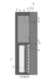
- FIG. 23 is a cross-sectional view showing an example of the configuration of a package according to the eighth embodiment
- FIG. 24 is a plan view showing an example of the configuration of a dummy chip of the package according to the eighth embodiment. Note that a in FIG. 24 shows a first configuration example of the dummy chip of the eighth embodiment, and b in FIG. 24 shows a second configuration example of the dummy chip of the eighth embodiment.
- a package 600 has an underfill 611 added to the package 400 of the fifth embodiment described above. Furthermore, the package 600 is provided with a dummy chip 652 in place of the dummy chip 152 of the fifth embodiment described above.
- the other configuration of the package 600 of the eighth embodiment is similar to the configuration of the package 400 of the fifth embodiment described above. Note that in the package 600 of the eighth embodiment, the antireflection film 431 of the fifth embodiment described above is omitted, but the antireflection film 431 may or may not be present.
- the distance D2 of a portion including the upper end of one surface facing the optical chip 411 is larger than the distance D1 of the other surface facing the optical chip 411.
- a recessed portion reaching the upper end of the surface may be formed on the surface.
- An underfill 611 is provided between the interposer substrate 130 and the optical chip 411 and between the optical chip 411 and the dummy chip 652.
- the material of the underfill 611 is, for example, thermosetting resin such as epoxy resin.
- the underfill 611 can be injected from a position where the distance between the optical chip 411 and the dummy chip 652 is D2.
- the interval D2 of a portion of the surface of the dummy chip 652 including the upper end of one surface facing the optical chip 411 is set to The distance between the surfaces is made larger than the distance D1. This makes it easier to fill the underfill 611 around the optical chip 411 placed in a position surrounded by the dummy chip 652, improving the reliability of the connection between the optical chip 411 and the interposer substrate 130. be able to.
- a dummy chip 653 b in FIG. 24 may be used.
- the distance D2 between the entire surfaces of one surface facing the optical chip 411 is larger than the distance D1 between the other surfaces facing the optical chip 411.
- FIG. 25 is a cross-sectional view showing an example of the configuration of a package according to the ninth embodiment.
- a package 700 is provided with a dummy chip 752 instead of the dummy chip 652 of the eighth embodiment described above.
- the rest of the configuration of the package 700 of the ninth embodiment is the same as the configuration of the package 600 of the eighth embodiment described above.
- the surface facing the optical chip 411 is provided with a forward tapered shape.
- Such a dummy chip 752 can be easily realized by processing the groove 155 into a forward tapered shape when forming the groove 155 in the dummy substrate 154 of FIG.
- An underfill 611 is provided between the interposer substrate 130 and the optical chip 411 and between the optical chip 411 and the dummy chip 752.
- a forward tapered shape is provided on the surface of the dummy chip 752 that faces the optical chip 411. This makes it easier to fill the underfill 611 around the optical chip 411 placed in a position surrounded by the dummy chip 752, thereby improving the reliability of the connection between the optical chip 411 and the interposer substrate 130. be able to.
- a forward tapered shape may be provided only on one surface facing 411.
- the semiconductor chip 421 placed in a position where the molding material 151 contacts and the optical chip 411 placed in a position surrounded by the dummy chip 152 are mounted on the interposer substrate 130.
- an optical chip 411 is mounted on a semiconductor chip mounted on an interposer substrate 130.
- FIG. 26 is a cross-sectional view showing an example of the structure of a package according to the tenth embodiment.
- a package 800 includes an optical chip 411, semiconductor chips 821 and 861, and a dummy chip 152.
- Semiconductor chips 821 and 861 are mounted on interposer substrate 830.
- Optical chip 411 is mounted on semiconductor chip 861.
- the dummy chip 152 is mounted on the semiconductor chip 861 so as to surround the optical chip 411.
- the dummy chip 152 can be placed on the semiconductor chip 861 apart from the optical chip 411.
- the semiconductor chip 861 is an example of a lower layer chip described in the claims.
- a semiconductor element is formed on the semiconductor chip 821.
- a signal processing circuit, a memory, an optical element, or the like may be formed on the semiconductor chip 821.
- an optical chip may be mounted on the interposer substrate 130.
- the optical chip may include a transparent resin and a transparent substrate.
- the semiconductor chip 821 includes a semiconductor substrate 822 and a wiring layer 823.
- the wiring layer 823 is formed on the semiconductor substrate 822.
- the wiring layer 823 is provided with wiring embedded in an insulating layer.
- a land electrode 815 to which a bump electrode 836 is connected can be formed on the wiring layer 823.
- a semiconductor element is formed on the semiconductor chip 861.
- a signal processing circuit, a memory, an optical element, or the like may be formed on the semiconductor chip 861.
- the semiconductor chip 861 includes a semiconductor substrate 862 and a wiring layer 863.
- the wiring layer 863 is formed on the semiconductor substrate 862.
- the wiring layer 863 is provided with wiring embedded in an insulating layer.
- a land electrode 864 to which the bump electrode 846 is connected can be formed on the wiring layer 863.
- a through electrode 865 is formed in the semiconductor substrate 862.
- the through electrode 865 is connected to the wiring layer 863.
- a land electrode 866 connected to the through electrode 865 is formed on the back side of the semiconductor substrate 862. Land electrode 866 is electrically connected to land electrode 415 via bump electrode 146.
- the interposer substrate 830 includes a support substrate 831 and a wiring layer 832.
- Land electrodes 833 and 843 are formed on the wiring layer 832. Wiring (not shown) may be formed in the wiring layer 832.
- Land electrodes 834 and 844 are formed on the back surface of support substrate 831. Further, through electrodes 835 and 845 are formed in the support substrate 831 and the wiring layer 832. Land electrodes 833 and 834 are electrically connected to each other via a through electrode 835. Land electrodes 843 and 844 are electrically connected to each other via a through electrode 845.
- a bump electrode 837 is formed on the land electrode 834, and a bump electrode 847 is formed on the land electrode 844.
- Land electrode 815 is connected to land electrode 833 via bump electrode 836.
- Land electrode 864 is connected to land electrode 844 via bump electrode 846.
- an underfill 819 is provided between the interposer substrate 830 and each of the semiconductor chips 821 and 861 and around each of the semiconductor chips 821 and 861.
- the material of the underfill 819 is, for example, thermosetting resin such as epoxy resin.
- a molding material 851 is arranged on the interposer substrate 830 so as to surround each of the semiconductor chip 821 and the dummy chip 152. At this time, the molding material 851 can contact the side surfaces of the semiconductor chip 821, the dummy chip 152, and the underfill 819. Furthermore, the position of the end of the molding material 851 in the lateral direction DL and the position of the end of the interposer substrate 830 in the lateral direction DL can coincide with each other.
- the surface of the molding material 851 is flattened at a position surrounding the semiconductor chip 821.
- the flat surface of the mold material 851 may be a polished surface.
- the position of the flat surface of the molding material 851 in the height direction DH can be made approximately equal to the position of the top surface of the semiconductor chip 821 in the height direction DH.
- the position of the flat surface of the dummy chip 152 in the height direction DH can be made approximately equal to the position of the flat surface of the mold material 851 in the height direction DH.
- the optical chip 411 is mounted on the semiconductor chip 861 mounted on the interposer substrate 830.
- three-dimensional integration of solidified chips can be achieved without increasing the mounting area of the interposer substrate 830.
- the wiring layer 413 of the optical chip 411 can be electrically connected to the outside while suppressing an increase in the wiring length. Therefore, it is possible to transmit and receive electrical signals to and from the optical chip 411 while suppressing an increase in the delay of the electrical signals transmitted and received between the optical chip and the optical chip 411.
- each chip can be electrically connected via a through electrode, and the optical chip can be placed on the top layer.
- the technology according to the present disclosure (this technology) can be applied to various products.
- the technology according to the present disclosure may be realized as a device mounted on any type of moving body such as a car, electric vehicle, hybrid electric vehicle, motorcycle, bicycle, personal mobility, airplane, drone, ship, robot, etc. It's okay.
- FIG. 27 is a block diagram showing a schematic configuration example of a vehicle control system, which is an example of a mobile object control system to which the technology according to the present disclosure can be applied.
- the vehicle control system 12000 includes a plurality of electronic control units connected via a communication network 12001.
- the vehicle control system 12000 includes a drive system control unit 12010, a body system control unit 12020, an outside vehicle information detection unit 12030, an inside vehicle information detection unit 12040, and an integrated control unit 12050.
- a microcomputer 12051, an audio/image output section 12052, and an in-vehicle network I/F (interface) 12053 are illustrated.
- the drive system control unit 12010 controls the operation of devices related to the drive system of the vehicle according to various programs.
- the drive system control unit 12010 includes a drive force generation device such as an internal combustion engine or a drive motor that generates drive force for the vehicle, a drive force transmission mechanism that transmits the drive force to wheels, and a drive force transmission mechanism that controls the steering angle of the vehicle. It functions as a control device for a steering mechanism to adjust and a braking device to generate braking force for the vehicle.
- the body system control unit 12020 controls the operations of various devices installed in the vehicle body according to various programs.
- the body system control unit 12020 functions as a keyless entry system, a smart key system, a power window device, or a control device for various lamps such as a headlamp, a back lamp, a brake lamp, a turn signal, or a fog lamp.
- radio waves transmitted from a portable device that replaces a key or signals from various switches may be input to the body control unit 12020.
- the body system control unit 12020 receives input of these radio waves or signals, and controls the door lock device, power window device, lamp, etc. of the vehicle.
- the external information detection unit 12030 detects information external to the vehicle in which the vehicle control system 12000 is mounted.
- an imaging section 12031 is connected to the outside-vehicle information detection unit 12030.
- the vehicle exterior information detection unit 12030 causes the imaging unit 12031 to capture an image of the exterior of the vehicle, and receives the captured image.
- the external information detection unit 12030 may perform object detection processing such as a person, car, obstacle, sign, or text on the road surface or distance detection processing based on the received image.
- the imaging unit 12031 is an optical sensor that receives light and outputs an electrical signal according to the amount of received light.
- the imaging unit 12031 can output the electrical signal as an image or as distance measurement information.
- the light received by the imaging unit 12031 may be visible light or non-visible light such as infrared rays.
- the in-vehicle information detection unit 12040 detects in-vehicle information.
- a driver condition detection section 12041 that detects the condition of the driver is connected to the in-vehicle information detection unit 12040.
- the driver condition detection unit 12041 includes, for example, a camera that images the driver, and the in-vehicle information detection unit 12040 detects the degree of fatigue or concentration of the driver based on the detection information input from the driver condition detection unit 12041. It may be calculated, or it may be determined whether the driver is falling asleep.
- the microcomputer 12051 calculates control target values for the driving force generation device, steering mechanism, or braking device based on the information inside and outside the vehicle acquired by the vehicle exterior information detection unit 12030 or the vehicle interior information detection unit 12040, Control commands can be output to 12010.
- the microcomputer 12051 realizes ADAS (Advanced Driver Assistance System) functions, including vehicle collision avoidance or shock mitigation, following distance based on vehicle distance, vehicle speed maintenance, vehicle collision warning, vehicle lane departure warning, etc. It is possible to perform cooperative control for the purpose of ADAS (Advanced Driver Assistance System) functions, including vehicle collision avoidance or shock mitigation, following distance based on vehicle distance, vehicle speed maintenance, vehicle collision warning, vehicle lane departure warning, etc. It is possible to perform cooperative control for the purpose of
- ADAS Advanced Driver Assistance System
- the microcomputer 12051 controls the driving force generating device, steering mechanism, braking device, etc. based on information about the surroundings of the vehicle acquired by the vehicle exterior information detection unit 12030 or the vehicle interior information detection unit 12040. It is possible to perform cooperative control for the purpose of autonomous driving, etc., which does not rely on operation.
- the microcomputer 12051 can output a control command to the body system control unit 12020 based on the information outside the vehicle acquired by the outside information detection unit 12030.
- the microcomputer 12051 controls the headlamps according to the position of the preceding vehicle or oncoming vehicle detected by the vehicle exterior information detection unit 12030, and performs cooperative control for the purpose of preventing glare, such as switching from high beam to low beam. It can be carried out.
- the audio and image output unit 12052 transmits an output signal of at least one of audio and images to an output device that can visually or audibly notify information to the occupants of the vehicle or to the outside of the vehicle.
- an audio speaker 12061, a display section 12062, and an instrument panel 12063 are illustrated as output devices.
- the display unit 12062 may include, for example, at least one of an on-board display and a head-up display.
- FIG. 28 is a diagram showing an example of the installation position of the imaging section 12031.
- the imaging unit 12031 includes imaging units 12101, 12102, 12103, 12104, and 12105.
- the imaging units 12101, 12102, 12103, 12104, and 12105 are provided, for example, at positions such as the front nose, side mirrors, rear bumper, back door, and the top of the windshield inside the vehicle 12100.
- An imaging unit 12101 provided in the front nose and an imaging unit 12105 provided above the windshield inside the vehicle mainly acquire images in front of the vehicle 12100.
- Imaging units 12102 and 12103 provided in the side mirrors mainly capture images of the sides of the vehicle 12100.
- An imaging unit 12104 provided in the rear bumper or back door mainly captures images of the rear of the vehicle 12100.
- the imaging unit 12105 provided above the windshield inside the vehicle is mainly used to detect preceding vehicles, pedestrians, obstacles, traffic lights, traffic signs, lanes, and the like.
- FIG. 28 shows an example of the imaging range of the imaging units 12101 to 12104.
- An imaging range 12111 indicates the imaging range of the imaging unit 12101 provided on the front nose
- imaging ranges 12112 and 12113 indicate imaging ranges of the imaging units 12102 and 12103 provided on the side mirrors, respectively
- an imaging range 12114 shows the imaging range of the imaging unit 12101 provided on the front nose.
- the imaging range of the imaging unit 12104 provided in the rear bumper or back door is shown. For example, by overlapping the image data captured by the imaging units 12101 to 12104, an overhead image of the vehicle 12100 viewed from above can be obtained.
- At least one of the imaging units 12101 to 12104 may have a function of acquiring distance information.
- at least one of the imaging units 12101 to 12104 may be a stereo camera including a plurality of image sensors, or may be an image sensor having pixels for phase difference detection.
- the microcomputer 12051 determines the distance to each three-dimensional object within the imaging ranges 12111 to 12114 and the temporal change in this distance (relative speed with respect to the vehicle 12100) based on the distance information obtained from the imaging units 12101 to 12104. In particular, by determining the three-dimensional object that is closest to the vehicle 12100 on its path and that is traveling at a predetermined speed (for example, 0 km/h or more) in approximately the same direction as the vehicle 12100, it is possible to extract the three-dimensional object as the preceding vehicle. can.
- a predetermined speed for example, 0 km/h or more
- the microcomputer 12051 can set an inter-vehicle distance to be secured in advance in front of the preceding vehicle, and perform automatic brake control (including follow-up stop control), automatic acceleration control (including follow-up start control), and the like. In this way, it is possible to perform cooperative control for the purpose of autonomous driving, etc., in which the vehicle travels autonomously without depending on the driver's operation.
- the microcomputer 12051 transfers three-dimensional object data to other three-dimensional objects such as two-wheeled vehicles, regular vehicles, large vehicles, pedestrians, and utility poles based on the distance information obtained from the imaging units 12101 to 12104. It can be classified and extracted and used for automatic obstacle avoidance. For example, the microcomputer 12051 identifies obstacles around the vehicle 12100 into obstacles that are visible to the driver of the vehicle 12100 and obstacles that are difficult to see. Then, the microcomputer 12051 determines a collision risk indicating the degree of risk of collision with each obstacle, and when the collision risk exceeds a set value and there is a possibility of a collision, the microcomputer 12051 transmits information via the audio speaker 12061 and the display unit 12062. By outputting a warning to the driver via the vehicle control unit 12010 and performing forced deceleration and avoidance steering via the drive system control unit 12010, driving support for collision avoidance can be provided.
- the microcomputer 12051 determines a collision risk indicating the degree of risk of collision with each obstacle, and when the collision risk exceed
- At least one of the imaging units 12101 to 12104 may be an infrared camera that detects infrared rays.
- the microcomputer 12051 can recognize a pedestrian by determining whether the pedestrian is present in the images captured by the imaging units 12101 to 12104.
- pedestrian recognition involves, for example, a procedure for extracting feature points in images captured by the imaging units 12101 to 12104 as infrared cameras, and a pattern matching process is performed on a series of feature points indicating the outline of an object to determine whether it is a pedestrian or not.
- the audio image output unit 12052 creates a rectangular outline for emphasis on the recognized pedestrian.
- the display unit 12062 is controlled to display the .
- the audio image output unit 12052 may control the display unit 12062 to display an icon or the like indicating a pedestrian at a desired position.
- the technology according to the present disclosure can not only be applied to the imaging section 12031 and the driver state detection section 12041 among the configurations described above, but also can realize at least part of the functions of the electronic control unit.
- the package 100 in FIG. 1 can be applied to the imaging section 12031 while realizing at least part of the functions of the electronic control unit.
- the present technology can also have the following configuration.
- a plurality of chips including an optical chip, a wiring layer on which the plurality of chips are mounted; and a molding material having a flattened surface, the molding material being arranged so as to surround at least one of the plurality of chips.
- the optical chip includes at least one of a light receiving element and a light emitting element.
- (8) further comprising a transparent member provided above the optical chip, The package according to any one of (1) to (7), wherein the molding material is positioned so as to surround the optical chip with the surface of the transparent member exposed.
- the transparent member includes at least one of a transparent resin and a transparent substrate.
- the transparent member includes an optically functional layer.
- At least a portion of the surfaces of the dummy chip, including the upper end of one surface facing the chip, is more similar to the chip surrounded by the dummy chip than the other surface facing the chip.
- the flattened surface is a polished surface where polishing is stopped at the position of the transparent member.
- a package comprising: a second chip mounted on the extended redistribution layer apart from the first chip, and on which a second wiring layer electrically connected to the extended redistribution layer is formed.
- the above further includes a molding material formed on the extended redistribution layer so as to surround at least one of the first chip and the second chip, and having a flattened surface.
- a step of sealing the chip and the dummy substrate with a molding material flattening the surface of the molding material and exposing the surface of the dummy substrate; removing at least a portion of the dummy substrate with the exposed surface;
- a method for manufacturing a package comprising the step of mounting an optical chip in a region from which the dummy substrate has been removed.
Landscapes
- Light Receiving Elements (AREA)
- Structures Or Materials For Encapsulating Or Coating Semiconductor Devices Or Solid State Devices (AREA)
- Solid State Image Pick-Up Elements (AREA)
- Engineering & Computer Science (AREA)
- Manufacturing & Machinery (AREA)
Abstract
Description
1.第1の実施の形態(表面が平坦化されたモールド材で周囲を囲むようにして透明部材が上方に配置された光学チップがインターポーザ基板上に実装された例)
2.第2の実施の形態(表面が平坦化されたモールド材で周囲を囲むようにして透明部材が上方に配置された光学チップが実装されたインターポーザ基板上に半導体チップを後付けした例)
3.第3の実施の形態(光学チップの上方に配置された透明部材上に光学的機能層を設けた例)
4.第4の実施の形態(モールド材で支持された透明部材が上方に配置された光学チップが実装された拡張再配線層上に半導体チップを後付けした例)
5.第5の実施の形態(モールド材上およびダミーチップ上に反射防止膜を設けた例)
6.第6の実施の形態(光学チップの上方に位置する透明部材がダミーチップで支持された例)
7.第7の実施の形態(表面が平坦化されたモールド材で周囲を囲まれた半導体チップが実装されたインターポーザ基板に後付けされた光学チップの上方に位置する透明基板がダミーチップで支持された例)
8.第8の実施の形態(アンダーフィルが注入される光学チップとダミーチップとの間の隙間を広げた例)
9.第9の実施の形態(ダミーチップの内面に順テーパ形状を持たせた例)
10.第10の実施の形態(光学チップが実装される下層チップを設けた例)
11.移動体への応用例
図1は、第1の実施の形態に係るパッケージの構成例を示す図である。なお、同図におけるaは、第1の実施の形態に係るパッケージの構成例を示す断面図、同図におけるbは、第1の実施の形態に係るパッケージの構成例を示す平面図である。同図におけるaは、同図におけるbのA1-A2線に沿って切断した断面図を示す。
上述の第1の実施の形態では、表面が平坦化されたモールド材151で周囲を囲むようにして透明基板118が上方に配置された光学チップ111をインターポーザ基板130上に実装していた。この第2の実施の形態では、表面が平坦化されたモールド材151で周囲を囲むようにして透明基板118が上方に配置された光学チップ111が実装されたインターポーザ基板130上に半導体チップを後付けする。
上述の第1の実施の形態では、表面が平坦化されたモールド材151で周囲を囲むようにして透明基板118が上方に配置された光学チップ111が実装されたインターポーザ基板130上に半導体チップ121が後付けされていた。この第3の実施の形態では、透明基板118上に光学的機能層を設け、その光学的機能層が設けられた光学チップの周囲がモールド材151で囲まれるようにする。
上述の第2の実施の形態では、表面が平坦化されたモールド材151で周囲を囲むようにして透明基板118が上方に配置された光学チップ111が実装されたインターポーザ基板130上に半導体チップ121を後付けされていた。この第4の実施の形態では、表面が平坦化されたモールド材151で周囲を囲むようにして透明基板118が上方に配置された光学チップ111が実装された拡張再配線層311上に半導体チップ121を後付けする。
上述の第2の実施の形態では、モールド材151が接触する位置に光学チップ111を設け、ダミーチップ152で囲まれる位置に半導体チップ121を設けていた。この第5の実施の形態では、モールド材151が接触する位置に半導体チップを設け、ダミーチップ152で囲まれる位置に光学チップを設ける。
上述の第1の実施の形態では、表面が平坦化されたモールド材151で周囲を囲むようにして透明基板118が上方に配置された光学チップ111をインターポーザ基板130上に実装していた。この第6の実施の形態では、光学チップの上方に位置する透明部材を支持するダミーチップを光学チップとともにインターポーザ基板130上に実装する。
上述の第5実施の形態では、モールド材151が接触する位置に半導体チップ421を設け、ダミーチップ152よりもトップ面が高い位置にある光学チップ411をダミーチップ152で囲まれる位置に設けていた。この第7の実施の形態では、モールド材151が接触する位置に半導体チップ421を設け、ダミーチップ152よりもトップ面が低い位置にある光学チップ511をダミーチップ152で囲まれる位置に設ける。
上述の第5の実施の形態では、モールド材151が接触する位置に配置された半導体チップ421と、ダミーチップ152で囲まれる位置に配置された光学チップ411とをインターポーザ基板130上に実装していた。この第8の実施の形態では、ダミーチップで囲まれる位置に配置された光学チップ411の周囲へのアンダーフィルの充填を容易化するために、ダミーチップと光学チップ411との間隔が拡大された領域を設ける。
上述の第8の実施の形態では、ダミーチップ152で囲まれる位置に配置された光学チップ411の周囲へのアンダーフィル611の充填を容易化するために、ダミーチップ152と光学チップ411との間隔が拡大された領域を設けていた。この第9の実施の形態では、ダミーチップで囲まれる位置に配置された光学チップ411の周囲へのアンダーフィル611の充填を容易化するために、ダミーチップの面のうち光学チップ411に対向する面に順テーパ形状を設ける。
上述の第5の実施の形態では、モールド材151が接触する位置に配置された半導体チップ421と、ダミーチップ152で囲まれる位置に配置された光学チップ411とをインターポーザ基板130上に実装していた。この第10の実施の形態では、インターポーザ基板130上に実装された半導体チップ上に光学チップ411を実装する。
本開示に係る技術(本技術)は、様々な製品へ応用することができる。例えば、本開示に係る技術は、自動車、電気自動車、ハイブリッド電気自動車、自動二輪車、自転車、パーソナルモビリティ、飛行機、ドローン、船舶、ロボット等のいずれかの種類の移動体に搭載される装置として実現されてもよい。
(1)光学チップを含む複数のチップと、
前記複数のチップが実装された配線層と、
前記複数のチップのうちの少なくともいずれか1つのチップの周囲を囲むように配置され、表面が平坦化されたモールド材と
を具備するパッケージ。
(2)前記モールド材の平坦面の高さ方向の位置は、前記複数のチップのうちの少なくともいずれか1つのチップのトップ面の高さ方向の位置に略等しい
前記(1)記載のパッケージ。
(3)前記光学チップは、受光素子および発光素子の少なくともいずれか1つを含む
前記(1)または(2)記載のパッケージ。
(4)前記複数のチップが実装された配線層は、インターポーザ基板に形成されている配線層または前記チップに形成された再配線層である
前記(1)から(3)のいずれかに記載のパッケージ。
(5)前記光学チップ以外のチップおよび前記モールド材のうちの少なくともいずれか1つの上に形成された反射防止膜をさらに具備する前記(1)から(4)のいずれかに記載のパッケージ。
(6)前記複数のチップのうちの少なくともいずれか1つのチップが実装される下層チップと、
前記下層チップに形成された貫通電極と
をさらに具備する前記(1)から(5)のいずれかに記載のパッケージ。
(7)前記モールド材で周囲が囲まれた状態で前記複数のチップのうちのいずれかのチップの周囲に離間して配置され、前記モールド材の平坦面と略同一の高さにトップ面が位置するダミーチップをさらに具備する前記(1)から(6)のいずれかに記載のパッケージ。
(8)前記光学チップの上方に設けられた透明部材をさらに具備し、
前記モールド材は、前記透明部材の表面が露出された状態で前記光学チップの周囲を囲むように位置する
前記(1)から(7)のいずれかに記載のパッケージ。
(9)前記透明部材は、透明樹脂および透明基板のうちの少なくともいずれか1つを含む
前記(8)記載のパッケージ。
(10)前記透明部材は、光学的機能層を備える
前記(9)記載のパッケージ。
(11)前記光学チップのトップ面は、前記モールド材のトップ面より低い位置にある
前記(7)記載のパッケージ。
(12)前記光学チップの上方に配置され、前記ダミーチップで支持された透明基板または光学部材をさらに具備する前記(11)記載のパッケージ。
(13)前記光学チップのトップ面は、前記モールド材のトップ面より高い位置にある
前記(7)記載のパッケージ。
(14)前記複数のチップのうちの少なくとも1つのチップと前記配線層との間および前記チップの周囲に設けられたアンダーフィルをさらに具備する前記(13)記載のパッケージ。
(15)前記ダミーチップの面のうち、前記チップに対向する1つの面の上端を含む少なくとも一部は、前記チップに対向する他の面に比べて、前記ダミーチップで周囲が囲まれるチップとの間隔が大きい
前記(14)記載のパッケージ。
(16)前記ダミーチップの面のうち、前記チップに対向する少なくとも1つの面は、順テーパ形状を備える
前記(14)記載のパッケージ。
(17)基板上に実装された光学チップと、
前記光学チップ上に設けられた透明部材と、
前記透明部材の表面が露出されるように表面が平坦化され、前記光学チップの周囲を囲むように前記基板上に形成された封止樹脂と
を具備するパッケージ。
(18)前記平坦化された表面は、前記透明部材の位置で研磨がストップされた研磨面である
前記(15)記載のパッケージ。
(19)第1配線層が形成された第1チップと、
前記第1配線層に電気的に接続され、前記第1チップの実装領域から横方向に拡張された拡張再配線層と、
前記第1チップと離間して前記拡張再配線層上に実装され、前記拡張再配線層に電気的に接続された第2配線層が形成された第2チップと
を具備するパッケージ。
(20)前記第1チップおよび前記第2チップのうちの少なくともいずれか1つのチップの周囲を囲むように前記拡張再配線層上に形成され、表面が平坦化されたモールド材をさらに具備する前記(17)記載のパッケージ。
(21)前記モールド材で周囲が囲まれた状態で前記第1チップおよび前記第2チップのうち1少なくともいずれか1つのチップの周囲に離間して前記拡張再配線層上に配置され、前記モールド材の表面と略同一の高さにトップ面が位置するダミーチップをさらに具備する前記(17)または(18)に記載のパッケージ。
(22)基板上に実装された光学チップと、
前記光学チップの周囲に離間して前記基板上に配置され、前記光学チップのトップ面から突出したダミーチップと、
前記光学チップの上方に配置され、前記ダミーチップで支持された透明部材と
を具備するパッケージ。
(23)前記ダミーチップの周囲を囲むように前記基板上に形成され、表面が平坦化されたモールド材をさらに具備する前記(20)記載のパッケージ。
(24)透明部材が上方に設けられた光学チップをダミー基板とともにモールド材で封止する工程と、
前記モールド材の表面を平坦化し、前記透明部材と前記ダミー基板の表面を露出させる工程と、
前記表面が露出された前記ダミー基板の少なくとも一部を除去する工程と、
前記ダミー基板が除去された領域にチップを実装する工程と
を具備するパッケージの製造方法。
(25)前記モールド材の表面の平坦化は、前記透明部材の位置でストップされる
前記(22)記載のパッケージの製造方法。
(26)チップとダミー基板とをモールド材で封止する工程と、
前記モールド材の表面を平坦化し、前記ダミー基板の表面を露出させる工程と、
前記表面が露出された前記ダミー基板の少なくとも一部を除去する工程と、
前記ダミー基板が除去された領域に光学チップを実装する工程と
を具備するパッケージの製造方法。
111 光学チップ
121 半導体チップ
130 インターポーザ基板
112 半導体層
113、123、132 配線層
114、131 支持基板
115、124、133、134、143、144 ランド電極
116 オンチップレンズ
117 透明樹脂
118 透明基板
122 半導体基板
135、145 貫通電極
136、137 バンプ電極
151 モールド材
152 ダミーチップ
153 接着材
Claims (26)
- 光学チップを含む複数のチップと、
前記複数のチップが実装された配線層と、
前記複数のチップのうちの少なくともいずれか1つのチップの周囲を囲むように配置され、表面が平坦化されたモールド材と
を具備するパッケージ。 - 前記モールド材の平坦面の高さ方向の位置は、前記複数のチップのうちの少なくともいずれか1つのチップのトップ面の高さ方向の位置に略等しい
請求項1記載のパッケージ。 - 前記光学チップは、受光素子および発光素子の少なくともいずれか1つを含む
請求項1記載のパッケージ。 - 前記複数のチップが実装された配線層は、インターポーザ基板に形成されている配線層または前記チップに形成された再配線層である
請求項1記載のパッケージ。 - 前記光学チップ以外のチップおよび前記モールド材のうちの少なくともいずれか1つの上に形成された反射防止膜をさらに具備する請求項1記載のパッケージ。
- 前記複数のチップのうちの少なくともいずれか1つのチップが実装される下層チップと、
前記下層チップに形成された貫通電極と
をさらに具備する請求項1記載のパッケージ。 - 前記モールド材で周囲が囲まれた状態で前記複数のチップのうちのいずれかのチップの周囲に離間して配置され、前記モールド材の平坦面と略同一の高さにトップ面が位置するダミーチップをさらに具備する請求項1記載のパッケージ。
- 前記光学チップの上方に設けられた透明部材をさらに具備し、
前記モールド材は、前記透明部材の表面が露出された状態で前記光学チップの周囲を囲むように位置する
請求項1記載のパッケージ。 - 前記透明部材は、透明樹脂および透明基板のうちの少なくともいずれか1つを含む
請求項8記載のパッケージ。 - 前記透明部材は、光学的機能層を備える
請求項9記載のパッケージ。 - 前記光学チップのトップ面は、前記モールド材のトップ面より低い位置にある
請求項7記載のパッケージ。 - 前記光学チップの上方に配置され、前記ダミーチップで支持された透明基板または光学部材をさらに具備する請求項11記載のパッケージ。
- 前記光学チップのトップ面は、前記モールド材のトップ面より高い位置にある
請求項7記載のパッケージ。 - 前記複数のチップのうちの少なくとも1つのチップと前記配線層との間および前記チップの周囲に設けられたアンダーフィルをさらに具備する請求項13記載のパッケージ。
- 前記ダミーチップの面のうち、前記チップに対向する1つの面の上端を含む少なくとも一部は、前記チップに対向する他の面に比べて、前記ダミーチップで周囲が囲まれるチップとの間隔が大きい
請求項14記載のパッケージ。 - 前記ダミーチップの面のうち、前記チップに対向する少なくとも1つの面は、順テーパ形状を備える
請求項14記載のパッケージ。 - 基板上に実装された光学チップと、
前記光学チップ上に設けられた透明部材と、
前記透明部材の表面が露出されるように表面が平坦化され、前記光学チップの周囲を囲むように前記基板上に形成された封止樹脂と
を具備するパッケージ。 - 前記平坦化された表面は、前記透明部材の位置で研磨がストップされた研磨面である
請求項16記載のパッケージ。 - 第1配線層が形成された第1チップと、
前記第1配線層に電気的に接続され、前記第1チップの実装領域から横方向に拡張された拡張再配線層と、
前記第1チップと離間して前記拡張再配線層上に実装され、前記拡張再配線層に電気的に接続された第2配線層が形成された第2チップと
を具備するパッケージ。 - 前記第1チップおよび前記第2チップのうちの少なくともいずれか1つのチップの周囲を囲むように前記拡張再配線層上に形成され、表面が平坦化されたモールド材をさらに具備する請求項19記載のパッケージ。
- 前記モールド材で周囲が囲まれた状態で前記第1チップおよび前記第2チップのうちの少なくともいずれか1つのチップの周囲に離間して前記拡張再配線層上に配置され、前記モールド材の表面と略同一の高さにトップ面が位置するダミーチップをさらに具備する請求項19記載のパッケージ。
- 基板上に実装された光学チップと、
前記光学チップの周囲に離間して前記基板上に配置され、前記光学チップのトップ面から突出したダミーチップと、
前記光学チップの上方に配置され、前記ダミーチップで支持された透明部材と
を具備するパッケージ。 - 前記ダミーチップの周囲を囲むように前記基板上に形成され、表面が平坦化されたモールド材をさらに具備する請求項22記載のパッケージ。
- 透明部材が上方に設けられた光学チップをダミー基板とともにモールド材で封止する工程と、
前記モールド材の表面を平坦化し、前記透明部材と前記ダミー基板の表面を露出させる工程と、
前記表面が露出された前記ダミー基板の少なくとも一部を除去する工程と、
前記ダミー基板が除去された領域にチップを実装する工程と
を具備するパッケージの製造方法。 - 前記モールド材の表面の平坦化は、前記透明部材の位置でストップされる
請求項24記載のパッケージの製造方法。 - チップとダミー基板とをモールド材で封止する工程と、
前記モールド材の表面を平坦化し、前記ダミー基板の表面を露出させる工程と、
前記表面が露出された前記ダミー基板の少なくとも一部を除去する工程と、
前記ダミー基板が除去された領域に光学チップを実装する工程と
を具備するパッケージの製造方法。
Priority Applications (4)
| Application Number | Priority Date | Filing Date | Title |
|---|---|---|---|
| CN202380030521.9A CN118946976A (zh) | 2022-04-08 | 2023-02-13 | 包装和用于制造包装的方法 |
| US18/851,881 US20250219037A1 (en) | 2022-04-08 | 2023-02-13 | Package and method for manufacturing package |
| KR1020247035365A KR20250002282A (ko) | 2022-04-08 | 2023-02-13 | 패키지 및 패키지의 제조방법 |
| EP23784530.0A EP4507010A4 (en) | 2022-04-08 | 2023-02-13 | HOUSING AND METHOD FOR MANUFACTURING HOUSING |
Applications Claiming Priority (2)
| Application Number | Priority Date | Filing Date | Title |
|---|---|---|---|
| JP2022064203 | 2022-04-08 | ||
| JP2022-064203 | 2022-04-08 |
Publications (1)
| Publication Number | Publication Date |
|---|---|
| WO2023195236A1 true WO2023195236A1 (ja) | 2023-10-12 |
Family
ID=88242824
Family Applications (1)
| Application Number | Title | Priority Date | Filing Date |
|---|---|---|---|
| PCT/JP2023/004705 Ceased WO2023195236A1 (ja) | 2022-04-08 | 2023-02-13 | パッケージおよびパッケージの製造方法 |
Country Status (6)
| Country | Link |
|---|---|
| US (1) | US20250219037A1 (ja) |
| EP (1) | EP4507010A4 (ja) |
| KR (1) | KR20250002282A (ja) |
| CN (1) | CN118946976A (ja) |
| TW (1) | TW202347527A (ja) |
| WO (1) | WO2023195236A1 (ja) |
Cited By (2)
| Publication number | Priority date | Publication date | Assignee | Title |
|---|---|---|---|---|
| WO2025115400A1 (ja) * | 2023-12-01 | 2025-06-05 | ソニーセミコンダクタソリューションズ株式会社 | 半導体パッケージ、半導体装置、および、半導体パッケージの製造方法 |
| WO2025234202A1 (ja) * | 2024-05-07 | 2025-11-13 | ソニーセミコンダクタソリューションズ株式会社 | 半導体パッケージ、半導体装置、および、半導体パッケージの製造方法 |
Citations (7)
| Publication number | Priority date | Publication date | Assignee | Title |
|---|---|---|---|---|
| JP2001127236A (ja) * | 1999-10-28 | 2001-05-11 | Mitsumi Electric Co Ltd | Icパッケージ |
| JP2005268440A (ja) * | 2004-03-17 | 2005-09-29 | Mitsumi Electric Co Ltd | 電子部品の製造方法及び電子部品 |
| JP2006270036A (ja) * | 2005-02-28 | 2006-10-05 | Sony Corp | ハイブリットモジュール及びその製造方法 |
| US20120104454A1 (en) * | 2010-10-28 | 2012-05-03 | Stmicroelectronics (Grenoble 2) Sas | Optical device, process for fabricating it and an electronic package comprising this optical device |
| JP2016166939A (ja) * | 2015-03-09 | 2016-09-15 | 富士通株式会社 | 光通信装置、光通信モジュール、及び光通信装置の製造方法 |
| US20190237454A1 (en) | 2018-02-01 | 2019-08-01 | Taiwan Semiconductor Manufacturing Company, Ltd. | Integrated circuit package and method of forming same |
| US20210210542A1 (en) * | 2018-09-21 | 2021-07-08 | Ningbo Semiconductor International Corporation | Photoelectric sensing integrated system and packaging method, lens module, and electronic device |
Family Cites Families (2)
| Publication number | Priority date | Publication date | Assignee | Title |
|---|---|---|---|---|
| US7791014B2 (en) * | 2005-03-09 | 2010-09-07 | Asahi Kasei Emd Corporation | Optical device and a method of manufacturing an optical device having a photoelectric conversion element and an optical adjustment element |
| US10866373B2 (en) * | 2018-06-27 | 2020-12-15 | Taiwan Semiconductor Manufacturing Company, Ltd. | Optical transceiver and manufacturing method thereof |
-
2023
- 2023-02-13 KR KR1020247035365A patent/KR20250002282A/ko active Pending
- 2023-02-13 CN CN202380030521.9A patent/CN118946976A/zh active Pending
- 2023-02-13 EP EP23784530.0A patent/EP4507010A4/en active Pending
- 2023-02-13 WO PCT/JP2023/004705 patent/WO2023195236A1/ja not_active Ceased
- 2023-02-13 US US18/851,881 patent/US20250219037A1/en active Pending
- 2023-03-23 TW TW112110825A patent/TW202347527A/zh unknown
Patent Citations (7)
| Publication number | Priority date | Publication date | Assignee | Title |
|---|---|---|---|---|
| JP2001127236A (ja) * | 1999-10-28 | 2001-05-11 | Mitsumi Electric Co Ltd | Icパッケージ |
| JP2005268440A (ja) * | 2004-03-17 | 2005-09-29 | Mitsumi Electric Co Ltd | 電子部品の製造方法及び電子部品 |
| JP2006270036A (ja) * | 2005-02-28 | 2006-10-05 | Sony Corp | ハイブリットモジュール及びその製造方法 |
| US20120104454A1 (en) * | 2010-10-28 | 2012-05-03 | Stmicroelectronics (Grenoble 2) Sas | Optical device, process for fabricating it and an electronic package comprising this optical device |
| JP2016166939A (ja) * | 2015-03-09 | 2016-09-15 | 富士通株式会社 | 光通信装置、光通信モジュール、及び光通信装置の製造方法 |
| US20190237454A1 (en) | 2018-02-01 | 2019-08-01 | Taiwan Semiconductor Manufacturing Company, Ltd. | Integrated circuit package and method of forming same |
| US20210210542A1 (en) * | 2018-09-21 | 2021-07-08 | Ningbo Semiconductor International Corporation | Photoelectric sensing integrated system and packaging method, lens module, and electronic device |
Non-Patent Citations (1)
| Title |
|---|
| See also references of EP4507010A4 |
Cited By (2)
| Publication number | Priority date | Publication date | Assignee | Title |
|---|---|---|---|---|
| WO2025115400A1 (ja) * | 2023-12-01 | 2025-06-05 | ソニーセミコンダクタソリューションズ株式会社 | 半導体パッケージ、半導体装置、および、半導体パッケージの製造方法 |
| WO2025234202A1 (ja) * | 2024-05-07 | 2025-11-13 | ソニーセミコンダクタソリューションズ株式会社 | 半導体パッケージ、半導体装置、および、半導体パッケージの製造方法 |
Also Published As
| Publication number | Publication date |
|---|---|
| KR20250002282A (ko) | 2025-01-07 |
| CN118946976A (zh) | 2024-11-12 |
| US20250219037A1 (en) | 2025-07-03 |
| EP4507010A1 (en) | 2025-02-12 |
| TW202347527A (zh) | 2023-12-01 |
| EP4507010A4 (en) | 2025-08-06 |
Similar Documents
| Publication | Publication Date | Title |
|---|---|---|
| JP7660061B2 (ja) | 半導体パッケージ、電子装置、および、半導体パッケージの製造方法 | |
| JP7802782B2 (ja) | 固体撮像素子、固体撮像素子の製造方法および電子機器 | |
| US20250219037A1 (en) | Package and method for manufacturing package | |
| US20250366251A1 (en) | Photodetection element and method of manufacturing photodetection element | |
| JP7462620B2 (ja) | 半導体パッケージ、半導体パッケージの製造方法、および、電子装置 | |
| US20250364513A1 (en) | Package, semiconductor device, and method for manufacturing package | |
| WO2023176122A1 (ja) | 半導体パッケージ、および、半導体パッケージの製造方法 | |
| WO2026083700A1 (ja) | 光学パッケージおよび光学パッケージの製造方法 | |
| WO2025248954A1 (ja) | パッケージおよびパッケージの製造方法 | |
| WO2025052679A1 (ja) | 電子デバイスおよび電子デバイスの製造方法 | |
| US20250386602A1 (en) | Solid-state imaging device | |
| WO2025115391A1 (ja) | パッケージおよびパッケージの製造方法 | |
| WO2024024278A1 (ja) | パッケージおよびパッケージの製造方法 | |
| WO2025204130A1 (ja) | パッケージ | |
| WO2024257483A1 (ja) | 半導体パッケージ、および、半導体パッケージの製造方法 | |
| WO2025079331A1 (ja) | パッケージおよびパッケージの製造方法 | |
| CN120202742A (zh) | 光检测装置 | |
| WO2025253766A1 (ja) | パッケージおよびパッケージの製造方法 | |
| WO2025159072A1 (ja) | 電子デバイスおよび電子デバイスの製造方法 | |
| JP2024016742A (ja) | 電子デバイス | |
| CN117897816A (zh) | 半导体封装、半导体设备以及半导体封装的制造方法 | |
| WO2026078991A1 (ja) | 半導体装置および半導体装置の製造方法 | |
| WO2024122177A1 (ja) | 半導体パッケージ、および、半導体パッケージの製造方法 | |
| WO2024057709A1 (ja) | 半導体パッケージ、および、電子装置 | |
| WO2025204106A1 (ja) | パッケージ |
Legal Events
| Date | Code | Title | Description |
|---|---|---|---|
| 121 | Ep: the epo has been informed by wipo that ep was designated in this application |
Ref document number: 23784530 Country of ref document: EP Kind code of ref document: A1 |
|
| WWE | Wipo information: entry into national phase |
Ref document number: 202380030521.9 Country of ref document: CN |
|
| WWE | Wipo information: entry into national phase |
Ref document number: 18851881 Country of ref document: US |
|
| WWE | Wipo information: entry into national phase |
Ref document number: 2023784530 Country of ref document: EP |
|
| NENP | Non-entry into the national phase |
Ref country code: DE |
|
| ENP | Entry into the national phase |
Ref document number: 2023784530 Country of ref document: EP Effective date: 20241108 |
|
| NENP | Non-entry into the national phase |
Ref country code: JP |
|
| WWP | Wipo information: published in national office |
Ref document number: 18851881 Country of ref document: US |