WO2023206400A1 - 显示基板以及显示装置 - Google Patents
显示基板以及显示装置 Download PDFInfo
- Publication number
- WO2023206400A1 WO2023206400A1 PCT/CN2022/090401 CN2022090401W WO2023206400A1 WO 2023206400 A1 WO2023206400 A1 WO 2023206400A1 CN 2022090401 W CN2022090401 W CN 2022090401W WO 2023206400 A1 WO2023206400 A1 WO 2023206400A1
- Authority
- WO
- WIPO (PCT)
- Prior art keywords
- sub
- pixel
- electrode
- edge
- layer
- Prior art date
- Legal status (The legal status is an assumption and is not a legal conclusion. Google has not performed a legal analysis and makes no representation as to the accuracy of the status listed.)
- Ceased
Links
Images




Classifications
-
- H—ELECTRICITY
- H10—SEMICONDUCTOR DEVICES; ELECTRIC SOLID-STATE DEVICES NOT OTHERWISE PROVIDED FOR
- H10K—ORGANIC ELECTRIC SOLID-STATE DEVICES
- H10K59/00—Integrated devices, or assemblies of multiple devices, comprising at least one organic light-emitting element covered by group H10K50/00
- H10K59/10—OLED displays
- H10K59/12—Active-matrix OLED [AMOLED] displays
- H10K59/131—Interconnections, e.g. wiring lines or terminals
-
- G—PHYSICS
- G09—EDUCATION; CRYPTOGRAPHY; DISPLAY; ADVERTISING; SEALS
- G09G—ARRANGEMENTS OR CIRCUITS FOR CONTROL OF INDICATING DEVICES USING STATIC MEANS TO PRESENT VARIABLE INFORMATION
- G09G3/00—Control arrangements or circuits, of interest only in connection with visual indicators other than cathode-ray tubes
- G09G3/20—Control arrangements or circuits, of interest only in connection with visual indicators other than cathode-ray tubes for presentation of an assembly of a number of characters, e.g. a page, by composing the assembly by combination of individual elements arranged in a matrix no fixed position being assigned to or needed to be assigned to the individual characters or partial characters
- G09G3/22—Control arrangements or circuits, of interest only in connection with visual indicators other than cathode-ray tubes for presentation of an assembly of a number of characters, e.g. a page, by composing the assembly by combination of individual elements arranged in a matrix no fixed position being assigned to or needed to be assigned to the individual characters or partial characters using controlled light sources
- G09G3/30—Control arrangements or circuits, of interest only in connection with visual indicators other than cathode-ray tubes for presentation of an assembly of a number of characters, e.g. a page, by composing the assembly by combination of individual elements arranged in a matrix no fixed position being assigned to or needed to be assigned to the individual characters or partial characters using controlled light sources using electroluminescent panels
- G09G3/32—Control arrangements or circuits, of interest only in connection with visual indicators other than cathode-ray tubes for presentation of an assembly of a number of characters, e.g. a page, by composing the assembly by combination of individual elements arranged in a matrix no fixed position being assigned to or needed to be assigned to the individual characters or partial characters using controlled light sources using electroluminescent panels semiconductive, e.g. using light-emitting diodes [LED]
- G09G3/3208—Control arrangements or circuits, of interest only in connection with visual indicators other than cathode-ray tubes for presentation of an assembly of a number of characters, e.g. a page, by composing the assembly by combination of individual elements arranged in a matrix no fixed position being assigned to or needed to be assigned to the individual characters or partial characters using controlled light sources using electroluminescent panels semiconductive, e.g. using light-emitting diodes [LED] organic, e.g. using organic light-emitting diodes [OLED]
- G09G3/3225—Control arrangements or circuits, of interest only in connection with visual indicators other than cathode-ray tubes for presentation of an assembly of a number of characters, e.g. a page, by composing the assembly by combination of individual elements arranged in a matrix no fixed position being assigned to or needed to be assigned to the individual characters or partial characters using controlled light sources using electroluminescent panels semiconductive, e.g. using light-emitting diodes [LED] organic, e.g. using organic light-emitting diodes [OLED] using an active matrix
- G09G3/3233—Control arrangements or circuits, of interest only in connection with visual indicators other than cathode-ray tubes for presentation of an assembly of a number of characters, e.g. a page, by composing the assembly by combination of individual elements arranged in a matrix no fixed position being assigned to or needed to be assigned to the individual characters or partial characters using controlled light sources using electroluminescent panels semiconductive, e.g. using light-emitting diodes [LED] organic, e.g. using organic light-emitting diodes [OLED] using an active matrix with pixel circuitry controlling the current through the light-emitting element
-
- H—ELECTRICITY
- H10—SEMICONDUCTOR DEVICES; ELECTRIC SOLID-STATE DEVICES NOT OTHERWISE PROVIDED FOR
- H10K—ORGANIC ELECTRIC SOLID-STATE DEVICES
- H10K59/00—Integrated devices, or assemblies of multiple devices, comprising at least one organic light-emitting element covered by group H10K50/00
- H10K59/10—OLED displays
- H10K59/12—Active-matrix OLED [AMOLED] displays
- H10K59/122—Pixel-defining structures or layers, e.g. banks
-
- G—PHYSICS
- G09—EDUCATION; CRYPTOGRAPHY; DISPLAY; ADVERTISING; SEALS
- G09G—ARRANGEMENTS OR CIRCUITS FOR CONTROL OF INDICATING DEVICES USING STATIC MEANS TO PRESENT VARIABLE INFORMATION
- G09G2300/00—Aspects of the constitution of display devices
- G09G2300/04—Structural and physical details of display devices
- G09G2300/0421—Structural details of the set of electrodes
- G09G2300/0426—Layout of electrodes and connections
-
- H—ELECTRICITY
- H10—SEMICONDUCTOR DEVICES; ELECTRIC SOLID-STATE DEVICES NOT OTHERWISE PROVIDED FOR
- H10K—ORGANIC ELECTRIC SOLID-STATE DEVICES
- H10K59/00—Integrated devices, or assemblies of multiple devices, comprising at least one organic light-emitting element covered by group H10K50/00
- H10K59/30—Devices specially adapted for multicolour light emission
- H10K59/35—Devices specially adapted for multicolour light emission comprising red-green-blue [RGB] subpixels
- H10K59/351—Devices specially adapted for multicolour light emission comprising red-green-blue [RGB] subpixels comprising more than three subpixels, e.g. red-green-blue-white [RGBW]
-
- H—ELECTRICITY
- H10—SEMICONDUCTOR DEVICES; ELECTRIC SOLID-STATE DEVICES NOT OTHERWISE PROVIDED FOR
- H10K—ORGANIC ELECTRIC SOLID-STATE DEVICES
- H10K59/00—Integrated devices, or assemblies of multiple devices, comprising at least one organic light-emitting element covered by group H10K50/00
- H10K59/80—Constructional details
- H10K59/82—Interconnections, e.g. terminals
Definitions
- At least one embodiment of the present disclosure relates to a display substrate and a display device.
- Transparent display is an important personalized display field in display technology. It refers to image display in a transparent state. Viewers can not only see the image in the display device, but also see the scene behind the display device.
- Transparent display devices using AMOLED technology usually divide each pixel into a display area and a non-luminous area. The display area is equipped with a pixel drive circuit and a light-emitting device to achieve image display, and the non-luminous area allows light to pass through.
- At least one embodiment of the present disclosure also provides a display substrate, which includes: a substrate substrate and a display unit. is provided on the base substrate and includes a display area; the display area includes a plurality of sub-display unit pixels, each of the plurality of sub-pixels includes a driving transistor and a light-emitting device, the driving transistor is configured to control a flow The size of the driving current through the light-emitting device, and includes a gate electrode, a first electrode and a second electrode; the light-emitting device is configured to receive the driving current and be driven by the driving current to emit light, and includes a first electrode , the first electrode is connected to the first pole of the driving transistor; the display unit further includes a pixel defining layer, the pixel defining layer defines opening areas of the plurality of sub-pixels; the plurality of sub-pixels of the display unit The two adjacent sub-pixels in the pixel are respectively the upper sub-pixel and the lower sub-pixel, and the direction perpendicular to the arrangement direction of the upper
- first edge and a second edge that intersects its first edge and is located on the first side of which its first edge is in the reference direction; the first edge of the first electrode of the upper sub-pixel to the upper sub-pixel
- the spacing between the first edges of the opening area of the pixel is a first spacing
- the spacing between the second edge of the first electrode of the upper sub-pixel and the second edge of the opening area of the upper sub-pixel is a second spacing. spacing, the first spacing is greater than the second spacing.
- the display substrate provided by at least one embodiment of the present disclosure further includes a first sub-scanning signal line, a second sub-scanning signal line, a data signal line and a detection signal line provided on the base substrate;
- the first sub-scanning signal line The signal line transmits a first scan signal
- the second sub-signal line transmits a second scan signal
- the data signal line transmits a data signal
- the detection signal line transmits a detection signal
- each sub-pixel in the plurality of sub-pixels further Includes: data writing transistor and detection transistor.
- the data writing transistor is configured to transmit the data signal to the driving transistor under the control of the first scan signal
- the detection transistor is configured to detect the detection signal using the detection signal under the control of the second scan signal.
- the orthographic projection of the channel region of the detection transistor on the base substrate is located within the orthographic projection of the first electrode on the base substrate, and, The first edge of the first electrode of the upper subpixel is located on the side of the channel region of the detection transistor of the upper subpixel that is close to the lower subpixel in the arrangement direction, and the first edge of the first electrode of the lower subpixel is An edge is located on a side of the channel region of the detection transistor of the lower sub-pixel that is close to the upper sub-pixel in the arrangement direction.
- the detection transistor includes a gate electrode, a first electrode and a second electrode, and the first electrode of the detection transistor of the upper sub-pixel is located at the second electrode thereof.
- the first pole of the detection transistor of the lower sub-pixel is located on the side of the second pole away from the upper sub-electrode; in the arrangement direction, the upper sub-pixel
- the distance between the first pole of the detection transistor and the first pole of the detection transistor of the lower sub-pixel is less than the length of the opening area of the upper sub-pixel in the arrangement direction and smaller than the length of the opening area of the lower sub-pixel in the arrangement direction. The length in the arrangement direction.
- the second sub-scanning signal line includes a ring portion, and the active layer of the ring portion and the detection transistor of the upper sub-pixel is perpendicular to the substrate.
- the portion that overlaps in the direction of the base substrate and the portion that overlaps with the active layer of the detection transistor of the lower sub-pixel in the direction perpendicular to the base substrate respectively constitute the gate electrode of the detection transistor of the upper sub-pixel.
- the orthographic projection of the annular portion on the base substrate constitutes an annular area, the second electrode of the detection transistor of the upper sub-pixel and the detection transistor of the lower sub-pixel
- the orthographic projections of the second pole on the base substrate are all located in the annular area.
- the first electrode of the lower sub-pixel has a first edge close to the upper sub-pixel and intersects its first edge and is located at the reference direction.
- the second edge of the first side upward;
- the opening area of the lower sub-pixel has a first edge close to the upper sub-pixel and intersects its first edge and is located on its first edge in the reference direction.
- the second edge of the first side the distance between the first edge of the first electrode of the lower sub-pixel and the first edge of the opening area of the lower sub-pixel is a third distance
- the first electrode of the lower sub-pixel The distance between the second edge and the second edge of the opening area of the lower sub-pixel is a fourth distance, and the third distance is greater than the fourth distance.
- the first electrode of the detection transistor in the upper sub-pixel, is electrically connected to the active layer of the detection transistor through an upper via hole; in the lower sub-pixel , the first pole of the detection transistor is electrically connected to the active layer of the detection transistor through the lower via hole; the second pole of the detection transistor of the upper sub-pixel is formed with the second pole of the detection transistor of the lower sub-pixel.
- the active layer of the detection transistor of the upper sub-pixel and the active layer of the detection transistor of the lower sub-pixel constitute a continuous integrated active layer
- the integrated electrode is connected to the upper sub-pixel through the middle via hole
- the integrated active layer is electrically connected; the orthographic projection of the first edge of the first electrode of the upper sub-pixel on the base substrate and the middle via hole are away from the lower sub-pixel in the arrangement direction.
- the orthographic projection of the edge of the first electrode on the base substrate at least partially overlaps, and the orthographic projection of the first edge of the first electrode of the lower sub-pixel on the base substrate is consistent with the arrangement of the middle via hole. Orthographic projections of edges directionally away from the upper sub-pixel on the base substrate at least partially overlap.
- the integrated electrode spans the gap between the first electrode of the upper sub-pixel and the first electrode of the lower sub-pixel along the arrangement direction, so Two ends of the integrated electrode that are opposite to each other in the arrangement direction are respectively located on both sides of the interval between the first electrode of the upper sub-pixel and the first electrode of the lower sub-pixel in the arrangement direction.
- the display unit further includes a conductive middle connection portion, the middle connection portion is located on a side of the active layer of the detection transistor close to the base substrate, and The orthographic projection of the intermediate connection portion on the base substrate is at least partially located on the orthographic projection of the interval between the first electrode of the upper sub-pixel and the first electrode of the lower sub-pixel on the base substrate.
- the detection signal line is connected to the middle connection part through a first connection via hole
- the integrated active layer is connected to the middle connection part through a second connection via hole
- the first of the upper sub-pixel The orthographic projection of the first edge of the electrode on the base substrate and the orthographic projection of the edge of the first connection via hole away from the lower sub-pixel in the arrangement direction on the base substrate, and the The orthographic projections of the edges of the second connection vias away from the lower sub-pixel in the arrangement direction on the base substrate at least partially overlap, and the first edge of the first electrode of the lower sub-pixel is at least partially overlapped.
- the orthographic projection on the base substrate and the orthographic projection of the edge of the second connection via hole away from the upper sub-pixel in the arrangement direction on the base substrate, and the second connection via hole The orthographic projections of the edges far away from the upper sub-pixels in the arrangement direction on the base substrate at least partially overlap.
- the third spacing and the first spacing are both larger than the spacing between the first electrode of the upper sub-pixel and the first electrode of the lower sub-pixel.
- the width in the arrangement direction is only larger than the spacing between the first electrode of the upper sub-pixel and the first electrode of the lower sub-pixel.
- the first electrode of the upper sub-pixel also has a third edge away from the lower sub-pixel, and the opening area of the upper sub-pixel further has a third edge away from the lower sub-pixel.
- the third edge of the upper sub-pixel; the distance between the third edge of the first electrode of the upper sub-pixel and the third edge of the opening area of the upper sub-pixel is a fifth pitch, and the first pitch is greater than the fifth spacing.
- the distance between the channel region of the driving transistor of the upper sub-pixel and the third edge of the opening region of the upper sub-pixel is greater than the distance between the channel region of the driving transistor of the upper sub-pixel and the third edge of the opening region of the upper sub-pixel. The distance between the channel region of the transistor and the first edge of the opening region of the upper sub-pixel is detected.
- the first electrode of the lower sub-pixel also has a third edge away from the upper sub-pixel
- the opening area of the lower sub-pixel also has a third edge away from the upper sub-pixel.
- the distance between the third edge of the pixel, the third edge of the lower sub-pixel and the third edge of the opening area of the lower sub-pixel is a sixth pitch, and the third pitch is greater than the sixth pitch.
- the distance between the channel region of the driving transistor of the lower sub-pixel and the third edge of the opening region of the lower sub-pixel is greater than the distance of the detection transistor of the lower sub-pixel.
- the distance between the channel region and the first edge of the opening region of the lower sub-pixel is greater than the distance of the detection transistor of the lower sub-pixel.
- the orthographic projection of the driving transistor and the data writing transistor on the base substrate is located at the orthographic projection of the opening area on the base substrate.
- at least part of the orthographic projection of the detection transistor on the base substrate is located outside the orthographic projection of the opening area on the base substrate.
- the first electrode in each sub-pixel of the plurality of sub-pixels, includes a first part and a second part arranged in the arrangement direction and spaced apart from each other, The first part of the first electrode and the second part of the first electrode are connected to the first pole of the driving transistor.
- the opening area includes a first sub-opening and a second sub-opening.
- the first electrode covers the first sub-opening, and the second part of the first electrode covers the second sub-opening; the edge of the first part of the first electrode of the upper sub-pixel close to the lower sub-pixel serves as the The first edge of the first electrode of the upper sub-pixel, the edge of the first part of the first electrode of the upper sub-pixel that intersects its first edge and is located on the first side of its first edge in the reference direction is used as the first edge of the first electrode of the upper sub-pixel.
- the second edge of the first electrode of the upper sub-pixel, and the edge of the second part of the first electrode of the upper sub-pixel away from the lower sub-pixel serves as the third edge of the first electrode of the upper sub-pixel;
- the edge of the first sub-opening of the above sub-pixel close to the lower sub-pixel serves as the first edge of the first sub-opening of the upper sub-pixel, and the edge of the first sub-opening of the upper sub-pixel intersects with its first edge and
- the edge of the first part of the first electrode of the lower sub-pixel close to the upper sub-pixel serves as the first edge of the first electrode of the lower sub-pixel, and the lower sub-pixel
- the orthographic projection of the channel region of the driving transistor on the base substrate is located on the first electrode
- the second part is within the orthographic projection on the base substrate
- the orthographic projection of the channel region of the data writing transistor on the base substrate is located on the third
- a first portion of an electrode is within an orthographic projection of the base substrate and is located adjacent to a second portion of the first electrode of an orthographic projection of the channel region of the detection transistor on the base substrate. side.
- the area of the opening area of the lower sub-pixel is larger than the area of the opening area of the upper sub-pixel, and the third pitch is greater than the first pitch.
- the first sub-scanning signal line extends along a first direction, and the first direction is the same as the reference direction;
- the display unit also includes a non-luminous area, and the The non-emitting area and the display area are arranged in the first direction and adjacent to the upper sub-pixel and the lower sub-pixel;
- the second edge of the first electrode of the upper sub-pixel is the upper sub-pixel
- the edge of the first electrode close to the non-emitting area, the second edge of the opening area of the upper sub-pixel is the edge of the opening area of the upper sub-pixel close to the non-emitting area;
- the second edge of the first electrode is the edge of the first electrode of the lower sub-pixel close to the non-emitting area, and the second edge of the opening area of the lower sub-pixel is the edge of the opening area of the lower sub-pixel close to the non-emitting area.
- the edge of the glowing area is the edge of the first electrode of the lower sub-pixel close to the non-emitting area.
- a plurality of sub-pixels of the display unit are arranged in an array, and the array includes a first pixel row extending along the first direction and a first pixel row extending along the first direction.
- the first pixel row includes adjacently arranged first sub-pixels and second sub-pixels
- the second pixel row includes adjacently arranged third sub-pixels and fourth sub-pixels
- the The length of each sub-pixel in the plurality of sub-pixels in the second direction is greater than the width of the sub-pixel in the first direction, and the first portion of the first electrode and the second portion of the first electrode are in are arranged in the second direction, and the area of the orthographic projection of the first sub-pixel on the base substrate and the area of the orthogonal projection of the third sub-pixel on the base substrate are both larger than the The area of the orthographic projection of the second sub-pixel on the base substrate and the area of the orthogonal projection of the fourth sub-pixel on the base substrate;
- the first sub-pixel serves as the upper sub-electrode
- the third sub-pixel serves as the lower sub-electrode
- the second sub-pixel serves as the upper sub-electrode
- the fourth sub-pixel serves as the lower sub
- the first sub-pixel emits red light
- the second sub-pixel emits blue light
- the third sub-pixel emits white light
- the fourth sub-pixel emits green light. Light.
- the display substrate provided by at least one embodiment of the present disclosure further includes: a first power line and a second power line.
- the first power line is connected to the first voltage terminal and is configured to provide a first power voltage to the plurality of sub-pixels, and includes a longitudinal portion extending overall along the second direction;
- the second power line is connected to the second voltage terminal and is configured In order to provide the plurality of sub-pixels with a second power supply voltage that is different from the first power supply voltage and extends along the second direction;
- the longitudinal portion of the first power supply line and the second power supply line are in the They are arranged at intervals in the first direction and are respectively located at the first edge of the display area in the first direction and the second edge of the display area opposite to the first edge in the first direction;
- the area between the edge of the longitudinal portion of the first power line away from the second power line and the edge of the second power line away from the longitudinal portion of the first power line is the display area.
- At least one embodiment disclosed also provides a display device, which includes any display substrate provided in the embodiments of the present disclosure.
- 1A is an overall plan view of a display substrate provided by an embodiment of the present disclosure
- 1B is a block diagram of a display substrate provided by at least one embodiment of the present disclosure.
- FIG. 2A is an equivalent circuit diagram of a pixel circuit of a display unit of a display substrate provided by an embodiment of the present disclosure
- 2B-2D are signal timing diagrams of the driving method of the pixel circuit provided by the embodiment of the present disclosure.
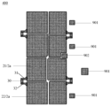
- 3A is a schematic plan view of a display unit of a display substrate provided by at least one embodiment of the present disclosure
- Figure 3B is a schematic diagram of the third sub-pixel in Figure 3A;
- Figure 3C is an enlarged view of the part including the connection structure in Figure 3B;
- Figure 4A is a schematic cross-sectional view along line A-A’ in Figure 3B;
- Figure 4B is a schematic cross-sectional view along line B-B’ and line C-C’ in Figure 3B;
- Figure 4C is a schematic cross-sectional view along line D-D' in Figure 3A;
- 4D is a schematic cross-section of a display substrate provided by another embodiment of the present disclosure at line A-A’ in FIG. 3B;
- FIG. 5A is a schematic plan view of the first conductive layer of the display unit shown in FIG. 3A;
- Figure 5B is a schematic plan view of the first insulating layer of the display unit shown in Figure 3A;
- FIG. 5C is a schematic plan view of the semiconductor layer of the display unit shown in FIG. 3A;
- FIG. 5D is a schematic plan view of the second conductive layer of the display unit shown in FIG. 3A;
- Figure 5E is a schematic plan view of the third insulating layer of the display unit shown in Figure 3A;
- Figure 5F is a schematic plan view of the third conductive layer of the display unit shown in Figure 3A;
- Figure 5G is a schematic plan view of the fourth insulating layer of the display unit shown in Figure 3A;
- Figure 5H is a schematic plan view of the fifth insulating layer of the display unit shown in Figure 3A;
- Figure 5I is a schematic plan view of the fourth conductive layer of the display unit shown in Figure 3A;
- Figure 5J is a schematic plan view of the fifth conductive layer of the display unit shown in Figure 3A;
- Figure 5K is a schematic plan view of the pixel defining layer of the display unit shown in Figure 3A;
- Figure 6A is an enlarged schematic view of part A of Figure 3A including at least one outer ring portion;
- Figure 6B is an enlarged schematic view of part B including at least one inner ring portion in Figure 3A;
- Figure 7 is another schematic cross-sectional view along line A-A' in Figure 3B;
- Figure 8A is an enlarged schematic diagram of part C in Figure 7;
- Figure 8B is an enlarged schematic view of another display substrate provided by an embodiment of the present disclosure at the position of part C in Figure 7;
- Figure 9 is a schematic plan view of part C shown in Figure 8A;
- Figure 10 is a schematic diagram of the arrangement of multiple sub-pixels of a display unit according to an embodiment of the present disclosure
- Figure 11A is a partial plan view of the first auxiliary unit H1 of the display unit shown in Figure 3A;
- Figure 11B is a schematic cross-sectional view along line E-E' in Figure 11A;
- Figure 11C is a schematic plan view showing the positional relationship of the second stacked layer, the fourth stacked layer, the fifth stacked layer and the eighth stacked layer in Figure 11B;
- Figure 12A is a partial plan view of the second auxiliary unit H2 of the display unit shown in Figure 3A;
- Figure 12B is a schematic cross-sectional view along line F-F' in Figure 12A;
- Figure 13A is a partial plan view of the third auxiliary unit H3 of the display unit shown in Figure 3A;
- Figure 13B is a schematic cross-sectional view along line G-G' in Figure 13A;
- FIG. 14A is a schematic diagram of a portion of the layers of the display unit shown in FIG. 3A including the pixel defining layer and the first electrode;
- Figure 14B is an enlarged schematic diagram of the local P0 shown by the dotted box in Figure 14A;
- FIG. 15 is a schematic diagram of a display device according to an embodiment of the present disclosure.
- the orthographic projection of a certain structure on the base substrate refers to the orthographic projection of the structure on the surface of the base substrate on which various transistors and various signal lines are disposed.
- structure A and structure B form a continuous one-piece structure means that structure A and structure B are made of the same material and have no seams between them. They are integrated structures with uniform texture, for example, through the same patterning process. Formed by craftsmanship.
- the letters A, B are used to refer to the corresponding structures described in the text.
- At least one embodiment of the present disclosure provides a display substrate, which includes: a base substrate and a display unit.
- a display unit is provided on the base substrate and includes a display area and a non-light-emitting area; the display area includes sub-pixels, and the sub-pixels include a driving transistor and a light-emitting device; the driving transistor is configured to control the flow through the The size of the driving current of the light-emitting device, and includes a gate electrode, a first electrode and a second electrode; the light-emitting device is configured to receive the driving current and be driven by the driving current to emit light, and includes a first electrode, the The first electrode includes a first part and a second part spaced apart from each other; the display unit also includes a connection structure and a first transfer electrode, the connection structure connects the first part of the first electrode and the second part of the first electrode , and includes a connection portion located in the non-emitting area; the first transfer electrode is connected to the first pole of the driving transistor and includes a
- At least one embodiment of the present disclosure also provides a display substrate, which includes: a substrate substrate, a display unit, a scanning signal line and a vertical signal line.
- a display unit is provided on the base substrate and includes a display area and a non-light-emitting area; the display area includes sub-pixels, the sub-pixels include a driving transistor and a light-emitting device, the driving transistor is configured to control the flow through the The size of the driving current of the light-emitting device, the light-emitting device is configured to receive the driving current and be driven by the driving current to emit light;
- the scanning signal line is provided on the base substrate, extends overall along the first direction, and passes through Scanning signals are transmitted through the non-luminescent area and the display area; vertical signal lines are provided on the base substrate and located in the display area, extending overall along a second direction that intersects with the first direction;
- the scanning signal line includes at least one outer loop portion, and each of the at least one outer loop portion includes a first conductive
- the first conductive line extends entirely along the first direction and extends from the non-light-emitting area to the display area; the second conductive line extends overall along the first direction and extends from the non-light-emitting area to the display area.
- the display area is spaced apart from the first conductive line in the second direction; both the first conductive line and the second conductive line overlap with the longitudinal signal line in a direction perpendicular to the base substrate.
- the scanning signal line includes a trunk portion extending in the first direction as a whole, and the first conductor and the second conductor are both electrically connected to the trunk portion.
- the first conductive line and the second conductive line transmit the same scanning signal, and the first conductive line and the second conductive line of at least one outer ring portion extend from the non-luminous area to the display area to overlap with the vertical signal line.
- At least one embodiment of the present disclosure also provides a display substrate, which includes: a substrate substrate and a display unit. is provided on the base substrate and includes a display area; the display area includes a plurality of sub-display unit pixels, each of the plurality of sub-pixels includes a driving transistor and a light-emitting device, the driving transistor is configured to control a flow The size of the driving current through the light-emitting device, and includes a gate electrode, a first electrode and a second electrode; the light-emitting device is configured to receive the driving current and be driven by the driving current to emit light, and includes a first electrode , the first electrode is connected to the first pole of the driving transistor; the display unit further includes a pixel defining layer, the pixel defining layer defines opening areas of the plurality of sub-pixels; the plurality of sub-pixels of the display unit The two adjacent sub-pixels in the pixel are respectively the upper sub-pixel and the lower sub-pixel, and the direction perpendicular to the arrangement direction of the upper
- first edge and a second edge that intersects its first edge and is located on the first side of which its first edge is in the reference direction; the first edge of the first electrode of the upper sub-pixel to the upper sub-pixel
- the spacing between the first edges of the opening area of the pixel is a first spacing
- the spacing between the second edge of the first electrode of the upper sub-pixel and the second edge of the opening area of the upper sub-pixel is a second spacing. spacing, the first spacing is greater than the second spacing.
- At least one embodiment of the present disclosure also provides a display substrate, which includes: a base substrate and a display unit provided on the base substrate.
- the display unit includes a display area and a non-light-emitting area, the display area includes sub-pixels, the sub-pixels include a driving transistor and a light-emitting device, the driving transistor is configured to control the size of the driving current flowing through the light-emitting device, the The light-emitting device is configured to receive the driving current and be driven by the driving current to emit light;
- the light-emitting device includes a first electrode and a common electrode, the common electrode is connected to a common voltage terminal;
- the display unit includes: an auxiliary electrode line , a first auxiliary electrode and an auxiliary insulating layer;
- the auxiliary electrode line includes a longitudinal portion located in the display area and a lateral portion located at least partially in the non-light-emitting area, the lateral portion is connected to the longitudinal portion;
- An auxiliary via hole is connected to the lateral part; the lateral part, the first auxiliary electrode and the first auxiliary via hole constitute an auxiliary unit, and the display unit includes a plurality of the auxiliary units; the auxiliary unit The transverse portion of the electrode line extends along a first direction, the longitudinal portion of the auxiliary electrode line extends along a second direction intersecting the first direction, and the plurality of auxiliary units are spaced apart from each other in the second direction.
- At least one embodiment disclosed also provides a display device, which includes any display substrate provided in the embodiments of the present disclosure.
- the display substrate provided by the present disclosure can be used in transparent display devices, such as large-size transparent display devices.
- Large-size transparent display devices include, for example, display panels larger than 55 inches.
- the transparent display device displays images in a transparent state, and viewers can not only see the displayed image in the display device, but also see the scene behind the display device.
- OLED Organic Light Emitting Diode
- PM passive matrix drive
- Active Matrix Active Matrix
- AM Active Matrix
- AMOLED is a current drive device and uses independent thin film transistors. (Thin Film Transistor, TFT for short) controls each sub-pixel, and each sub-pixel can be driven to emit light continuously and independently.
- TFT Thin Film Transistor
- a transparent display device using AMOLED technology usually divides each pixel into a display area and a non-luminous area. The display area is provided with a pixel driving circuit and a light-emitting device 20 to achieve image display, and the non-luminous area allows light transmission.
- Deterioration of characteristics of the thin film transistor or internal short circuit failure may occur in the wiring of the display device, the manufacturing process of the thin film transistor, or the manufacturing process of the organic light emitting diode.
- a pixel or sub-pixel can become a dark spot because current or voltage is not applied to the organic light emitting diode connected to the thin film transistor.
- the driving thin film transistor cannot be driven normally, and the voltage applied to the source electrode is directly applied to the drain electrode without turning on/off, thereby The subpixels always remain on, and bright spots appear as a result.
- the bright spots are easily seen by the user's eyes due to good visibility, the bright spots degrade the display quality. For this reason, even if only one bright spot appears on the display area, the display device is considered to be defective, thereby causing a problem that the display device cannot be manufactured as a final product.
- dark spots or bright spots in a transparent display device or a top-emission large-size display device may be seen by the user's eyes, there is a need for a solution that can avoid or minimize the dark spots or bright spots.
- At least one embodiment of the present disclosure provides a display substrate, which includes: a base substrate and a display unit.
- a display unit is provided on the base substrate and includes a display area and a non-light-emitting area; the display area includes sub-pixels, and the sub-pixels include a driving transistor and a light-emitting device; the driving transistor is configured to control the flow through the The size of the driving current of the light-emitting device, and includes a gate electrode, a first electrode and a second electrode; the light-emitting device is configured to receive the driving current and be driven by the driving current to emit light, and includes a first electrode, the The first electrode includes a first part and a second part spaced apart from each other; the display unit also includes a connection structure and a first transfer electrode, the connection structure connects the first part of the first electrode and the second part of the first electrode , and includes a connection portion located in the non-emitting area; the first transfer electrode is connected to the first pole of the driving transistor and includes a
- FIG. 1A is an overall plan view of a display substrate provided by an embodiment of the present disclosure.
- the display substrate 10 includes a base substrate 1 and a display unit P disposed on the base substrate.
- it includes a plurality of display units P.
- the plurality of display units P are arranged in an array.
- Each display unit P includes a display area 11 and a non-emitting area 12.
- the display area 11 includes sub-pixels.
- the display unit P includes a plurality of sub-pixels arranged in an array.
- the array includes a first pixel row extending along the first direction D1.
- each display unit P includes adjacently arranged first sub-pixels P1 and second sub-pixels P2, and the second pixel row includes adjacently arranged third sub-pixels P3 and Four sub-pixels P4.
- 1A takes the display area 11 of each display unit P as an example including a first sub-pixel P1, a second sub-pixel P2, a third sub-pixel P3 and a fourth sub-pixel P4.
- each display The display area 11 of unit P also includes more than four or less than 4 sub-pixels.
- the first sub-pixel P1 may be a red sub-pixel (R) emitting red light
- the second sub-pixel P2 may be a green sub-pixel (G) emitting green light
- the second sub-pixel P2 may be a white sub-pixel emitting white light
- the fourth sub-pixel P4 may be a blue sub-pixel (B) that emits blue light.
- the emission colors of the first sub-pixel P1, the second sub-pixel P2, the second sub-pixel P2 and the fourth sub-pixel P4 are not limited to the above situation, and the embodiment of the present disclosure does not limit this.
- each sub-pixel may be a rectangle, a rhombus, a pentagon, or a hexagon.
- four sub-pixels may be arranged horizontally in parallel to form an RWBG pixel arrangement.
- the four sub-pixels may be arranged in a square, diamond or vertical arrangement, which is not limited in this disclosure.
- FIG. 2A is an equivalent circuit schematic diagram of the pixel circuit of four sub-pixels of one display unit P shown in FIG. 1A . 1A and 2A, each of the first sub-pixel P1, the second sub-pixel P2, the third sub-pixel P3 and the fourth sub-pixel P4 includes a pixel circuit, and the pixel circuit includes a driving transistor T1 and a light-emitting device 20; display Area 11 is a light-emitting area, used to display images; the non-light-emitting area is a non-light-emitting area, not used to display images, and can see through the environment on the non-display side.
- the driving transistor T1 is configured to control the magnitude of the driving current flowing through the light emitting device 20 and includes a gate electrode, a first electrode and a second electrode.
- the light emitting device 20 is configured to receive a driving current and be driven by the driving current to emit light.
- the display substrate is an organic light-emitting diode (OLED) display substrate, and the light-emitting device 20 is an OLED.
- OLED organic light-emitting diode
- FIG. 1B is a block diagram of a display substrate provided by at least one embodiment of the present disclosure.
- each of the first subpixel P1 , the second subpixel P2 , the third subpixel P3 and the fourth subpixel P4 includes a pixel circuit that drives the light emitting device 20 to emit light.
- the display substrate may further include a plurality of scanning lines and a plurality of data lines for providing scanning signals (control signals) and data signals for the plurality of sub-pixels, thereby driving the plurality of sub-pixels.
- the display substrate may further include power lines, detection lines, etc.
- the pixel circuit includes a driving sub-circuit for driving the light-emitting device 20 to emit light and a detection sub-circuit for detecting the electrical characteristics of the sub-pixel to achieve external compensation.
- the embodiments of the present disclosure do not limit the specific structure of the pixel circuit.
- FIG. 1B shows a schematic diagram of a 3T1C pixel circuit used in the display substrate.
- the pixel circuit may further include a compensation circuit, a reset circuit, etc.
- the pixel circuit may also have a 4T1C, 5T1C, 5T2C, 6T1C, 7T1C or 8T1C structure, for example.
- the embodiments of the present disclosure are not limited to this.
- each display unit P further includes a first scanning signal line G1, a second scanning signal line G2, a first power supply line vdd, a second power supply line line vss, four data signal lines D (in Figure 2A, the four data signal lines D are the first to fourth data signal lines D1 to D4 respectively, the first sub-pixel P1 is connected to the first data signal line D1, and the second The sub-pixel P2 is connected to the second data signal line D2, the third sub-pixel P3 is connected to the third data signal line D3, the fourth sub-pixel P4 is connected to the fourth data signal line D4), a detection signal line S and a detection signal line S respectively correspond to Four pixel circuits for four word pixels P1 ⁇ P2 ⁇ P3 ⁇ P4.
- first scanning signal line G1 and the second scanning signal line G2 extend along the first direction D1 and are arranged along the second direction D2.
- the first direction D1 intersects the second direction D2.
- the first direction intersects the second direction D2.
- Direction D2 is vertical.
- the first power supply line vdd, the data signal lines D1 ⁇ D2 ⁇ D3 ⁇ D4 and the detection signal line S may extend along the second direction D2 and be arranged along the first direction D1.
- four data signal lines D and one detection signal line S are provided between the first power line vdd and the second power line vss, and two of the four data signal lines D1 ⁇ D2 ⁇ D3 ⁇ D4 are D3 ⁇ D4.
- the other two data signal lines D1 ⁇ D2 among the four data signal lines D are located between the detection signal line S and the second power line vss.
- four sub-pixels are formed between the first power line vdd and the second power line vss by setting four data signal lines D1 ⁇ D2 ⁇ D3 ⁇ D4 and one detection signal line S.
- Four sub-pixels are also formed by arranging a first power supply line vdd, a second power supply line vss and four data signal lines D1 ⁇ D2 ⁇ D3 ⁇ D4.
- 2B-2D are signal timing diagrams of the driving method of the pixel circuit provided by the embodiment of the present disclosure.
- the pixel circuit of each of the first sub-pixel P1, the second sub-pixel P2, the third sub-pixel P3 and the fourth sub-pixel P4 includes a first transistor T1, a second transistor T2 , the third transistor T3 and the storage capacitor Cst.
- the first scanning signal line G1 is connected to the gate electrode of the second transistor T2 in each sub-pixel
- the second scanning signal line G2 is connected to the gate electrode of the third transistor T3 in each sub-pixel.
- the first electrode of the second transistor T2 is electrically connected to the first capacitor electrode of the storage capacitor Cst and the gate electrode of the first transistor T1, the data signal line is connected to the second electrode of the second transistor T2, and the second transistor
- the second electrode of T2 is configured to receive the data signal GT
- the second transistor T2 is a data transistor, and is configured to write the data signal DT into the gate of the first transistor T1 and the storage capacitor Cst in response to the first control signal G1
- the first electrode of a transistor T1 is electrically connected to the second capacitor electrode of the storage capacitor Cst, and is configured to be electrically connected to the first electrode of the light emitting element 20.
- the first power supply line VDD is connected to the second electrode of the first transistor T1.
- a second terminal of a transistor T1 is configured to receive a first power supply voltage V1 (for example, a high power supply voltage VDD).
- the first transistor T1 is a driving transistor and is configured to be at a voltage of a gate of the first transistor T1 .
- the current used to drive the light-emitting element is controlled under control;
- the first electrode of the third transistor T3 is electrically connected to the first electrode of the first transistor T1 and the second capacitor electrode of the storage capacitor Cst, and the detection signal line S is connected to the third transistor T3.
- the second pole is connected, and the second pole of the third transistor T3 is configured to be connected to the first detection line S to be connected to the external detection circuit 11 .
- the third transistor T3 is a detection transistor and is configured to detect in response to the second control signal G2
- the electrical characteristics of the sub-pixel are used to achieve external compensation; the electrical characteristics include, for example, the threshold voltage and/or carrier mobility of the first transistor T1, or the threshold voltage, driving current, etc. of the light-emitting element.
- the external detection circuit 11 is, for example, a conventional circuit including a digital-to-analog converter (DAC), an analog-to-digital converter (ADC), etc., which will not be described in detail in the embodiments of the present disclosure.
- the transistors used in the embodiments of the disclosure may be thin film transistors, field effect transistors, or other switching devices with the same characteristics.
- thin film transistors are used as examples for explanation.
- the source and drain of the transistor used here can be symmetrical in structure, so there can be no structural difference between the source and drain.
- one of the poles is directly described as the first pole and the other pole is the second pole.
- transistors can be divided into N-type and P-type transistors according to their characteristics.
- the turn-on voltage is a low-level voltage (for example, 0V, -5V, -10V or other suitable voltages), and the turn-off voltage is a high-level voltage (for example, 5V, 10V or other suitable voltages) );
- the turn-on voltage is a high-level voltage (for example, 5V, 10V or other suitable voltages), and the turn-off voltage is a low-level voltage (for example, 0V, -5V, -10V or other suitable voltages) voltage).
- the transistor in FIG. 1B is an N-type transistor as an example, but this is not intended to limit the present disclosure.
- Figure 2A shows the working principle of the pixel circuit during the display process.
- Figure 2B shows the signal timing diagram of the pixel circuit during the display process.
- Figures 2C and 2D show The signal timing diagram of the pixel circuit during the detection process is shown.
- the display process of each frame image includes data writing and resetting stage 1 and lighting stage 2.
- Figure 2B shows the timing waveforms of each signal in each stage.
- a working process of the 3T1C pixel circuit includes: in the data writing and reset phase 1, the first control signal G1 and the second control signal G2 are both turn-on signals, the second transistor T2 and the third transistor T3 are turned on, and the data signal DT is transmitted to the gate of the first transistor T1 through the second transistor T2, the first switch K1 is closed, and the analog-to-digital converter transmits the signal to the first electrode of the light-emitting element (such as the anode of the OLED) through the first detection line 130 and the third transistor T3.
- the first electrode of the light-emitting element such as the anode of the OLED
- the first transistor T1 When the reset signal is written, the first transistor T1 is turned on and generates a driving current to charge the first electrode of the light-emitting element to the operating voltage; in the light-emitting phase 2, the first control signal G1 and the second control signal G2 are both off signals. Due to the storage Due to the bootstrap effect of the capacitor Cst, the voltage across the storage capacitor Cst remains unchanged. The first transistor T1 works in a saturated state with a constant current and drives the light-emitting element to emit light.
- FIG. 2C shows a signal timing diagram of the pixel circuit when detecting the threshold voltage.
- a working process of the 3T1C pixel circuit includes: the first control signal G1 and the second control signal G2 are both turn-on signals, the second transistor T2 and the third transistor T3 are turned on, and the data signal DT is transmitted to the third transistor through the second transistor T2.
- the node S is charged until the first transistor is turned off, and the digital-to-analog converter samples the voltage on the first detection line 130 to obtain the threshold voltage of the first transistor T1.
- This process may be performed, for example, when the display device is turned off.
- FIG. 2D shows a signal timing diagram of the pixel circuit when detecting the threshold voltage.
- a working process of the 3T1C pixel circuit includes: in the first stage, the first control signal G1 and the second control signal G2 are both turn-on signals, the second transistor T2 and the third transistor T3 are turned on, and the data signal DT passes through the second The transistor T2 transmits to the gate of the first transistor T1; the first switch K1 is closed, and the analog-to-digital converter writes a reset signal to the first electrode (node S) of the light-emitting element through the first detection line 130 and the third transistor T3; in In the second stage, the first control signal G1 is a turn-off signal, the second control signal G1 is a turn-on signal, the second transistor T2 is turned off, the third transistor T3 is turned on, and the first switch K1 and the second switch K2 are turned off.
- the first transistor T1 Floating the first detection line 130; due to the bootstrap effect of the storage capacitor Cst, the voltage across the storage capacitor Cst remains unchanged, the first transistor T1 works in a saturated state with unchanged current and drives the light-emitting element to emit light, and then digital-to-analog conversion
- the device samples the voltage on the first detection line 130 and combines it with the magnitude of the light-emitting current to calculate the carrier mobility in the first transistor T1. For example, this process can be performed during the blanking phase between display phases.
- the electrical characteristics of the first transistor T1 can be obtained and the corresponding compensation algorithm can be implemented.
- the display substrate 10 may further include a data driving circuit 03 and a scan driving circuit 04 .
- the data driving circuit 03 is configured to emit a data signal, such as the above-mentioned data signal DT, as needed (such as an image signal input to the display device); the pixel circuit of each sub-pixel is also configured to receive the data signal and apply the data signal to the third The gate of a transistor.
- the scan driving circuit 04 is configured to output various scanning signals, including, for example, the above-mentioned first control signal G1 and the second control signal G2, which is, for example, an integrated circuit chip (IC) or a gate driving circuit (GOA) directly prepared on the display substrate. ).
- the display substrate 10 further includes a control circuit 02 .
- the control circuit 02 is configured to control the data driving circuit 03 to apply the data signal, and to control the gate driving circuit 03 to apply the scanning signal.
- An example of the control circuit 02 is a timing control circuit (T-con).
- the control circuit 02 can be in various forms, for example, including a processor 021 and a memory 022.
- the memory 022 includes executable code, and the processor 021 runs the executable code to perform the above detection method.
- the processor 021 may be a central processing unit (CPU) or other form of processing device with data processing capabilities and/or instruction execution capabilities, and may include, for example, a microprocessor, a programmable logic controller (PLC), etc.
- CPU central processing unit
- PLC programmable logic controller
- memory 022 may include one or more computer program products, which may include various forms of computer-readable storage media, such as volatile memory and/or non-volatile memory.
- Volatile memory may include, for example, random access memory (RAM) and/or cache memory (cache), etc.
- Non-volatile memory may include, for example, read-only memory (ROM), hard disk, flash memory, etc.
- One or more computer program instructions may be stored on the computer-readable storage medium, and the processor 021 may execute the functions desired by the program instructions.
- Various application programs and various data can also be stored in the computer-readable storage medium, such as the electrical characteristic parameters obtained in the above detection method.
- FIG. 3A is a schematic plan view of a display unit P of the display substrate 10 provided by at least one embodiment of the present disclosure
- FIG. 3B is a schematic view of the third sub-pixel P3 in FIG. 3A
- FIG. 3C is a partial L including a connection structure in FIG. 3B An enlarged view
- Figure 4A is a schematic cross-sectional view along line AA' in Figure 3B.
- the light emitting device 20 includes a first electrode 2 including a first portion 21 and a second portion 22 spaced apart from each other.
- the display unit P also includes: a connection structure 3 and a first transfer electrode 4 .
- connection structure 3 connects the first part 21 of the first electrode 2 and the second part 22 of the first electrode 2 and includes a connection part 30 located in the non-light-emitting area 12; the first transfer electrode 4 and the first electrode T1s of the driving transistor T1 Connected to and including a portion located in the non-luminescent region 12 , the connecting portion 30 is electrically connected in the non-luminescent region 12 to a portion of the first transfer electrode 4 located in the non-luminescent region 12 .
- multiple parts of the first electrode 2 such as the first part 21 and the second part 22, are connected to the first electrode T1s of the driving transistor T1 through the connection part 30 and the first transfer electrode 4.
- the opening area of a sub-pixel includes a first sub-opening 601 and a second sub-opening 602 (as shown in Figure 5K).
- the first sub-opening 601 and the second sub-opening 602 is the area corresponding to the first part 21 of the first electrode 2 and the second part 22 of the first electrode 2 respectively.
- the first part 21 of an electrode 2 covers the first sub-opening 601, and the second part 22 of the first electrode 2
- the second sub-opening 602 is covered.
- the first portion 21 of the first electrode 2 and the second portion 22 of the first electrode 2 are electrically connected to the connection portion 30 located in the non-luminous area 12 in the non-luminous area 12, and then are located in the display area through the first transfer electrode 4.
- the part 11 is connected to the first electrode T1s of the driving transistor T1.
- the first transfer electrode 4 is located in the display.
- the portion of the region 11 is connected to the first electrode T1s of the driving transistor T1 so that a via hole for connecting the connection portion 30 to the first transfer electrode 4 is made in the non-light-emitting region 12 .
- the embodiment of the present disclosure is The position of the non-light-emitting area 12 corresponding to the connection part 30 makes the alignment process of making via holes for connecting the connection part 30 and the first transfer electrode 4 easier, and the yield rate can be significantly improved.
- the longitudinal portion vdd1 of the first power line vdd and the second power line vss are spaced apart in the first direction D1 and are respectively located in the display area 11 in the first direction D1
- the area between the edges of the longitudinal portion vdd1 of the first power line vdd is the display area 11 .
- the light-emitting element is an organic light-emitting diode, including a first electrode 2 , a second electrode 24 , and a light-emitting layer 23 located between the first electrode 2 and the second electrode 24 .
- the first electrode is a material with a high work function to serve as an anode, such as an ITO/Ag/ITO stacked structure, or an ITO/Al/ITO stacked structure (sandwich structure), or ITO/(Al+Ag) /ITO laminated structure (sandwich structure).
- the first electrode is not limited to the above-mentioned sandwich structure, and the material of the first electrode is not limited to the above-mentioned types.
- the second electrode 24 is a material with a low work function to serve as a cathode, such as a semi-transmissive metal or metal alloy material, such as an Ag/Mg alloy material.
- the light-emitting element has a top-emission structure, the first electrode 2 is reflective and the second electrode 122 is transmissive or semi-transmissive.
- the first transfer electrode 4 includes a first transfer portion 41, which is located in the display area 11 and connected to the first pole of the driving transistor T1;
- the portion of the connecting electrode 4 located in the non-light-emitting area 12 includes a second connecting portion 42, the second connecting portion 42 is connected to the first connecting portion 41, the connecting portion 30 and the second connecting portion 42 are arranged in different layers, and,
- the connection part 30 is connected to the second adapter part 42 in the non-light-emitting area 12 through the first via hole V0.
- the display unit P further includes a second transfer electrode 5 .
- the second transfer electrode 5 is located in the non-light-emitting area 12 and is located between the connection portion 30 and the second transfer electrode 5 in a direction perpendicular to the base substrate 1 . between the transfer portion 42 and the orthographic projection of the second transfer electrode 5 on the base substrate 1 and the orthographic projection of the connection portion 30 on the base substrate 1 and the orthographic projection of the second transfer portion 5 on the base substrate 1 .
- the orthographic projections all at least partially overlap; the connection part 30 is connected to the second transfer part 42 through the second transfer electrode 5 and is connected in segments, thereby reducing the possibility that the connection part 30 is directly connected to the second transfer part 42 through a via hole. Hole depth improves the manufacturing yield of display substrates.
- the display substrate 10 further includes a first insulating layer 101 , a second insulating layer 102 located on a side of the first insulating layer 101 away from the substrate 1 , and a second insulating layer 102 located on a side of the second insulating layer 102 away from the substrate 1 .
- the third insulating layer 103 on one side of the base substrate 1, the fourth insulating layer 104 located on the second transfer electrode 5 away from the third insulating layer 103 in the direction perpendicular to the base substrate 1, and the interlayer insulating layer 105 is vertical It is located on the side of the fourth insulating layer 104 away from the third insulating layer 103 in the direction of the base substrate 1 .
- the first via V0 includes a first sub-via V01 penetrating the first insulating layer 101 and the third insulating layer 103.
- the second transfer electrode 5 is connected to the second transfer part 42 through the first sub-via V01; display substrate 10 also includes that the first via V0 also includes a second sub-via V02 penetrating the fourth insulating layer 104, and the connection part 30 is connected to the second transfer electrode 5 through the second sub-via V02, thereby realizing the connection part 30 It is connected to the second adapter part 42 through multi-level via holes.
- the first adapter part 41 and the second adapter part 42 are a continuous integrally formed structure.
- the material of the first transfer electrode 4 is a metal material, such as copper, aluminum, chromium, copper alloy, aluminum alloy, chromium alloy, manganese alloy, etc., but is not limited to the types listed above.
- the display unit P further includes an interlayer insulating layer 105.
- the interlayer insulating layer 105 is located in the display area 11 and not in the non-emitting area 12. In a direction perpendicular to the base substrate 1, the interlayer insulating layer 105 is located on the first electrode. 2 and the second transfer electrode 5.
- the first electrode 2 is electrically connected to the first electrode T1s of the driving transistor T1 through the opening O1 penetrating the interlayer insulating layer 5 in a direction perpendicular to the base substrate 1 .
- the opening O1 is connected to the second sub-via hole V02, and the first electrode 2 enters the second sub-via hole V02 through the opening O1 penetrating the interlayer insulating layer 5 and is connected to the second transfer electrode 5.
- the orthographic projection of the first via hole on the base substrate 1 is located within the orthographic projection of the opening O1 on the base substrate 1 , that is, the second sub-via hole V02 and the first sub-via hole V01 are on the base substrate 1
- the orthographic projection of is located within the orthographic projection of the opening O1 on the base substrate 1 .
- the first electrode 2 can be electrically connected to the first electrode T1s of the driving transistor T1 through the larger opening O1 of the interlayer insulating layer 105 in the non-light-emitting area, thereby facilitating the realization of the connection portion 30 and the second connection in the non-light-emitting area.
- the connection of the electrode 5 and the creation of a larger opening O1 in the non-emitting area have lower requirements on the manufacturing process and are easy to implement.
- the accuracy of making the opening O1 is high and has little impact on other surrounding structures.
- the insulation layer in the display area 11 is avoided.
- the problem of low through-hole production yield and great impact on surrounding structures is caused by the space limitation of mid-hole drilling.
- the interlayer insulating layer 105 is located in the display area 11 and is not located in the non-emitting area 12A. That is, the interlayer insulating layer 105 does not include a portion located in the non-emitting area 12A.
- the portion of the material layer used to form the interlayer insulating layer 105 located in the non-emitting region 12A is completely removed through a patterning process, thereby forming an opening O1 in the non-emitting region in the same layer as the interlayer insulating layer 105.
- the orthographic projection of the opening O1 on the base substrate 1 is located in the non-light-emitting area 12A, and the area of the orthographic projection of the opening O1 on the base substrate 1 is equal to the area of the non-light-emitting area 12A.
- the production of the interlayer insulating layer 105 can be further reduced compared to the solution of making via holes in the non-display area 12A for passing the first electrode 2 Difficulty, improve the production yield of display substrates.
- the area of the orthographic projection of the opening O1 on the base substrate 1 is larger than the area of the orthogonal projection of a sub-pixel adjacent to the opening O1 on the base substrate 1 .
- the maximum width W1 of the opening O1 is greater than the maximum width W2 of a sub-pixel.
- a sub-pixel adjacent to the opening O1 Take P3 as an example.
- the orthographic projection of the opening O1 on the base substrate 1 is located in the non-emitting area 12A, and the area of the orthographic projection of the opening O1 on the base substrate 1 is smaller than the non-emitting area. 12A area. That is, in the process of making the interlayer insulating layer 105, part of the portion of the material layer used to form the interlayer insulating layer 105 located in the non-emitting region 12A is removed through a patterning process, thereby forming the opening O1, which is A larger via hole passes through the interlayer insulating layer 105 , and the edge of the opening O1 is at least partially surrounded by the material of the interlayer insulating layer 105 .
- Other features and corresponding technical effects of the embodiment shown in Figure 4D are the same as those in Figure 4A. Please refer to the description of Figure 4A.
- the interlayer insulating layer 105 has a fault at the junction of the display area 11 and the non-emitting area 12 , that is, there is a step structure 001 on the edge of the interlayer insulating layer 105 close to the non-emitting area 12 , and the first electrode 2
- the step structure 001 is covered to extend across the step structure 001 to the non-light-emitting area 12 .
- the interlayer insulating layer 105 is no longer provided on the side of the step structure 001 close to the non-light-emitting area 12 , so that the connection portion 30 can be located on the step structure 001 Compared with the solution in which the interlayer insulating layer 105 is located in the display area 11 and the non-emitting area 12, this embodiment can avoid making a through-layer in the interlayer insulating layer 105.
- the via hole of the insulating layer 105 used to connect the connecting portion 30 to the second transfer electrode 5 simplifies the manufacturing process of the display substrate and is of great significance to improving the yield of the display substrate; because the interlayer insulating layer 105 is perpendicular to The thickness in the direction of the base substrate 1 is relatively large.
- the thickness of the interlayer insulating layer 105 in the direction perpendicular to the base substrate 1 is greater than 6000 Angstroms to satisfy its function of insulation and serving as a flat layer. If the interlayer insulation is made through
- the via holes of the layer 105 for connecting the connection portion 30 to the second transfer electrode 5 have different sizes in the direction parallel to the base substrate from the via holes used for other purposes in the interlayer insulating layer 105. For example, the size of the via hole in the direction parallel to the base substrate is required to be larger. Therefore, when multiple via holes penetrating the interlayer insulating layer 105 are produced through the same patterning process, it is difficult to meet these different sizes at the same time.
- the above solution of the embodiment of the present disclosure can avoid making a via hole penetrating the interlayer insulating layer 105 for connecting the connecting portion 30 to the second transfer electrode 5 in the interlayer insulating layer 105 , thereby avoiding the above problem.
- the material of the interlayer insulating layer 105 is an organic insulating material.
- the organic insulating material includes resin material, acrylic material, etc., for example, it can be polyimide (PI), acrylate, epoxy resin, polymethylmethacrylate. ester (PMMA), etc., but are not limited to the types listed above.
- the interlayer insulating layer 105 is a planarization layer.
- the first insulating layer 101, the second insulating layer 102, the third insulating layer 103, and the fourth insulating layer 104 are, for example, inorganic insulating layers, such as silicon oxide, silicon nitride, silicon oxynitride, etc., silicon oxides, etc. Nitride or silicon oxynitride, or aluminum oxide, titanium nitride, etc. include metal oxynitride insulating materials.
- the display substrate 10 further includes first signal lines G1/G2 and second signal lines D1 to D4 provided on the base substrate 1 .
- the first signal line G1/G2 transmits the scanning signal; for example, the first signal line includes a first sub-scanning signal line G1 and a second sub-scanning signal line G2; the first sub-scanning signal line G1 transmits the first scanning signal, and the second sub-scanning signal line G2
- the signal line G2 transmits the second scanning signal; for example, the first scanning signal and the second scanning signal may be progressive scanning signals, for example, the first scanning signal and the second scanning signal are the same scanning signal, please refer to the above-mentioned Figure 2B; or, In other embodiments, the first scanning signal and the second scanning signal are different signals.
- the second signal lines D1 to D4 transmit the data signal DT;
- the first signal lines extend as a whole along the first direction D1, and the second signal lines D1 to D4 as a whole extend along the second direction D2 that intersects the first direction D1;
- the sub-pixel further includes a data writing transistor T2 configured to transmit the data signal to the driving transistor T1 under the control of the first scan signal.
- first direction D1 includes extending generally along the first direction D1, and at least it suffices that it extends entirely along the first direction D1.
- first signal line extending overall along the first direction D1 may have a certain curved portion, or, in some examples, the edge of the strip extending overall along the second direction D2 It may not be a smooth line, for example, its edge may have burrs or jagged edges. In short, it is sufficient as long as the overall extension trend is along the first direction D1.
- extending as a whole along the second direction D2 This is also true for any reference in this disclosure to extending in a certain direction as a whole.
- connection structure 3 includes at least two extension parts, and the at least two extension parts include: a first extension part 31 and a second extension part 32 .
- the first extension part 31 has a first end and a second end opposite to the first end, and extends from the display area 11 to the non-light emitting area 12 .
- the first end of the first extension part 31 is connected to the first part 21 of the first electrode 2 connected, the second end of the first extension part 31 is located in the non-light-emitting area 12;
- the second extension part 32 has a first end and a second end opposite to the first end, and extends from the display area 11 to the non-light-emitting area 12,
- the first end of the two extension parts 32 is connected to the second part 22 of the first electrode 2, and the second end of the second extension part 32 is located in the non-light-emitting area 12;
- the connection part 30 is connected to the second end of the first extension part 31 and the second end of the first extension part 31.
- the second ends of the two extension parts 32 are connected.
- the connecting part 30 is connected to the first part 21 of the first electrode 2 and the second part 22 of the first electrode 2 respectively through at least one channel, that is, the first extending part 31 and the second extending part 32.
- a sub-pixel such as the When a dark spot or other display failure occurs in one of the opening area of the three sub-pixels P3 corresponding to the first part 21 of the first electrode 2 and the area corresponding to the second part 22 of the first electrode 2
- the area can be One of the first extension part 31 and the second extension part 32 corresponding to the area where dark spots or other display defects occur is cut off, so that the area where dark spots or other display defects occur is not displayed, and the first extension part 31 and the second extension part 32
- the two extending portions 32 are in the form of strips extending along the first direction D1, which are easy to cut, thereby facilitating the repair of sub-pixels and improving the display quality.
- the second end of the first extension part 31 has a first cutable part 310
- the second end of the second extension part 32 has a second cuttable part 320;
- the maximum width W SP of the interval between the first portion 21 of the first electrode 2 and the second portion 22 of the first electrode 2 in the second direction D2 is smaller than the maximum width W SP of the connecting portion 30 in the second direction D2
- the maximum width W C on the second direction D2 is to ensure that the connecting portion 30 has sufficient width to connect the first portion 21 of the first electrode 2 and the second portion 22 of the first electrode 2 , and so that the first electrode 2
- the distance between the first part 21 and the second part 22 of the first electrode 2 should not be too large to occupy too much space, so as to achieve a high PPI display panel at the same time.
- the first part 21 of the first electrode 2 , the second part 22 of the first electrode 2 , the first extension part 31 , the second extension part 32 and the connecting part 30 are a continuous one-piece structure to simplify the structure of the display substrate.
- the above-mentioned continuous one-piece structure can be formed by performing the same patterning process on the same material layer, which simplifies the manufacturing process of the display substrate.
- each sub-pixel further includes a first power line vdd.
- the first power line vdd is connected to the first voltage terminal VDD and is configured to provide a first power voltage to the sub-pixel.
- the first power line vdd is connected to the first power line vdd.
- the first pole of the driving transistor T1 is arranged in the same layer and includes a vertical portion vdd1.
- the vertical portion vdd1 extends overall along the second direction D2 and is connected to its adjacent sub-pixels; for example, the first power line vdd also includes The transverse portion vdd2 is electrically connected to the longitudinal portion and extends overall along the first direction D1 to be connected to each sub-pixel of the display unit, thereby providing the first power supply voltage to each sub-pixel of the display unit.
- the horizontal portion vdd2 in Figure 3B is connected to the third sub-pixel P3 and the fourth sub-pixel P4, and Figure 3A also includes another bar connected to the longitudinal portion vdd2 and connected to the first sub-pixel P1 and the second sub-pixel P2.
- the horizontal part vdd2 is provided to realize supplying the first power supply voltage from the vertical part vdd1 to each sub-pixel of the display unit.
- the first extension part 31 and the second extension part 32 extend across the first power line vdd and the second signal line to the non-light-emitting area 12 to connect with the connection part located in the non-light-emitting area 12 .
- the non-luminescent area 12 and the display area 11 are arranged in the second direction D2
- the first part 21 of the first electrode 2 and the second part 22 of the first electrode 2 are arranged in the second direction D2
- the first Both the extending portion 31 and the second extending portion 32 extend along the first direction D1 as a whole.
- Such an arrangement can coordinate the positions of the first part 21 of the first electrode 2 and the second part 22 of the first electrode 2 and the non-emitting areas corresponding to the sub-pixels in which they are located, thereby facilitating the separation between the first part 21 and the second part 22 of the first electrode 2.
- the second part 22 of the first electrode 2 respectively leads the first extension part 31 and the second extension part 32 to the non-light-emitting area 12, so as to facilitate the connection between the connection part 30 located in the non-light-emitting area 12 and the first part 21 of the first electrode 2.
- the second part 22 of the first electrode 2 is connected.
- the non-light-emitting area 12 includes a first non-light-emitting area 12A located on a first side of the display area 11 in the first direction D1 and a second non-light-emitting area 12B located on A second side of the display area 11 opposite to its first side in the first direction D1; the first sub-pixel P1 and the third sub-pixel P3 are adjacent to the first non-light-emitting area 12A, the second sub-pixel P2 and the fourth sub-pixel
- the pixel P4 is adjacent to the first non-emitting area 12A; a connection structure 3 is provided corresponding to each of the plurality of sub-pixels, and the connection structure 3 connects the first part 21 of the first electrode 2 of the adjacent sub-pixel and the first electrode 2
- the second part 22; the connection part 30 corresponding to the connection structure 3 of the first sub-pixel P1 and the connection part 30 corresponding to the connection structure 3 of the third sub-pixel P3 are located in the first non-emitting area 12A; corresponding to the
- the first signal lines G1/G2 that provide scanning signals to the first sub-pixel P1, the second sub-pixel P2, the third sub-pixel P3 and the fourth sub-pixel P4 are located in the first pixel row and the first pixel row.
- the planar patterns of the first sub-pixel P1 and the second sub-pixel P2 are symmetrical with respect to the symmetry axis extending along the second direction D2
- the planar pattern of the third sub-pixel P3 is symmetrical with the symmetry axis of the fourth sub-pixel P4
- the planar pattern of the first non-light-emitting area 12A and the second non-light-emitting area 12B is symmetrical with respect to the symmetry axis to rationally utilize space and improve the uniformity of the display substrate, thereby improving the uniformity of display in the display area and reducing the difficulty of manufacturing the display substrate.
- the display unit P further includes a pixel defining layer 6
- the pixel defining layer 6 includes: a first part 61 and a second part 62 .
- the first portion 61 is located between the first electrodes 2 of adjacent sub-pixels to define an opening area 60 of the sub-pixel, and the light-emitting layer 23 of the light-emitting device 20 is at least located in the opening area 60 .
- the second portion 62 is located between the first portion 21 of the first electrode 2 and the second portion 22 of the first electrode 2 to separate the first portion 21 of the first electrode 2 from the second portion 22 of the first electrode 2 .
- the orthographic projection of the connecting portion 30 on the base substrate 1 is located within the orthographic projection of the first portion 61 of the pixel defining layer 6 on the base substrate 1 to avoid the connecting portion 30 and the pixel defining layer 6
- Each of the first parts 61 occupies an independent space to save space, and the first part 61 of the pixel definition layer 6 is used to protect the connection part 30 .
- the light-emitting element of the display substrate 10 may adopt a top-emission structure.
- each sub-pixel taking the third sub-pixel P3 as an example, also includes a first capacitor C1; the first capacitor C1 includes a first plate Ca and a second plate Cb; the first plate Ca It is electrically connected to the gate electrode T1g of the driving transistor T1 and is arranged on the same layer as the gate electrode of the driving transistor T1.
- the first plate Ca is an integrated structure that is continuous with the gate electrode T1g of the driving transistor T1; the second plate Cb is on the substrate.
- the orthographic projection on the substrate 1 at least partially overlaps the orthographic projection of the first electrode plate Ca on the base substrate 1 .
- the sub-pixel taking the third sub-pixel P3 as an example, also includes a second capacitor C2.
- the second capacitor C2 includes a first plate Ca and a third plate Cc;
- the third plate Cc includes The overlapping portion and the non-overlapping portion, the orthographic projection of the overlapping portion on the base substrate 1 overlaps with the orthographic projection of the first electrode plate Ca on the base substrate 1, and the orthographic projection of the non-overlapping portion on the base substrate 1 overlaps with the orthographic projection of the first electrode plate Ca on the base substrate 1
- the orthographic projection of the electrode plate Ca on the base substrate 1 does not overlap and at least partially overlaps the orthographic projection of the second electrode plate Cb on the base substrate 1 .
- Figure 4B is a schematic cross-sectional view along line BB' and line CC' in Figure 3B. As shown in Figure 4B, the non-overlapping portion is connected to the second plate Cb through the second via V2, and the third plate Cc is multiplexed as the first adapter portion 41 , that is, the first adapter portion 41 and the second plate Cb are connected through the second via hole V2 to simplify the structure and manufacturing process of the display substrate 10 .
- the second plate Cb and the first electrode T1s of the driving transistor T1 are arranged on the same layer.
- the second plate Cb and the first electrode T1s of the driving transistor T1 have a continuous integrated structure, so as to realize the third
- the diode plate Cb is electrically connected to the first pole T1s of the driving transistor T1, thereby realizing the electrical connection between the first switching part 41 and the first pole T1s of the driving transistor T1.
- the integrated structure in which the third plate Cc is multiplexed as the first connecting portion 41 and the second plate Cb and the first electrode T1s of the driving transistor T1 greatly simplifies the structure and manufacturing process of the display substrate 10 .
- the first electrode T1s of the driving transistor T1 is connected to the active layer T1a of the driving transistor T1 through a plurality of via holes to reduce the contact resistance; for example, the plurality of via holes are spaced apart from each other along the second direction D2 arrangement; for example, the first electrode T1s of the driving transistor T1 is connected to the active layer T1a of the driving transistor T1 through three vias: via V91, via V92 and via V93.
- the via V91, via V92 and via V93 are all penetrating the second insulating layer 102 and the third insulating layer 103 .
- the number of the multiple via holes is not limited to three, and can be designed as needed.
- Figure 5A is a schematic plan view of the first conductive layer of the display unit shown in Figure 3A;
- Figure 5B is a schematic plan view of the first insulating layer of the display unit shown in Figure 3A;
- Figure 5C is a semiconductor of the display unit shown in Figure 3A
- Figure 5D is a schematic plan view of the second conductive layer of the display unit shown in Figure 3A;
- Figure 5E is a schematic plan view of the third insulating layer of the display unit shown in Figure 3A;
- Figure 5F is a schematic plan view of the third insulating layer of the display unit shown in Figure 3A
- Figure 5G is a schematic plan view of the third conductive layer of the display unit shown in Figure 3A;
- Figure 5H is a schematic plan view of the fifth insulating layer of the display unit shown in Figure 3A;
- the display substrate 10 includes a first conductive layer 100 and a first insulating layer 101 sequentially stacked on the base substrate 1 in a direction from close to the base substrate 1 to away from the base substrate 1 .
- the fifth insulating layer 105 is also the above-mentioned interlayer insulating layer 105.
- the materials of the semiconductor layer 600 include but are not limited to silicon-based materials (amorphous silicon a-Si, polycrystalline silicon p-Si, etc.), metal oxide semiconductors (IGZO, ZnO, AZO, IZTO, etc.) and organic materials (hexathiophene, Polythiophene, etc.).
- silicon-based materials amorphous silicon a-Si, polycrystalline silicon p-Si, etc.
- metal oxide semiconductors IGZO, ZnO, AZO, IZTO, etc.
- organic materials hexathiophene, Polythiophene, etc.
- the first conductive layer 100 includes a first transfer part 41, a second transfer part 42 and a third plate Cc;
- the semiconductor layer 600 includes the active layer T1a of the driving transistor T1, the data The active layer T2a of the transistor T2 and the active layer T3a of the detection transistor T3;
- the second conductive layer 200 includes the first sub-scanning signal line G1 and the second sub-scanning signal line G2, the gate electrode T1g of the driving transistor T1, and the data transistor T2
- the gate T2g and the gate T3g of the detection transistor T3, the first plate Ca, the lateral portion vdd2 of the first power line vdd and the auxiliary power line vdd3, the auxiliary power line vdd3 corresponds to the vertical portion vdd1 of the first power line vdd Extends along the second direction D2, and is electrically connected to the vertical portion vdd1 of the first power line vdd through a plurality of vias V4 penetr
- the auxiliary power line vdd3 is electrically connected to the lateral part vdd2, thereby realizing the electrical connection between the lateral part vdd2 and the vertical part vdd1.
- the auxiliary power line vdd3 and the lateral portion vdd2 are arranged on the same layer, and both are located on the second conductive layer 200 .
- the auxiliary power line vdd3 and the horizontal part vdd2 have a continuous integrated structure.
- the third conductive layer 300 includes a first pole T1s and a second pole T1d of the driving transistor T1, a first pole T2s and a second pole T2d of the data transistor T2, a first pole T3s and a second pole T3d of the detection transistor T3, and a data line. D1 ⁇ D2 ⁇ D3 ⁇ D4, the detection signal line S, and the vertical part vdd1 of the first power line vdd. It can be seen from FIG. 4A and FIG. 5H that the above-mentioned interlayer insulating layer 105 is only provided in the display area 11 , and there is no interlayer insulating layer 105 in the non-light-emitting area 12 .
- the first portion 21 of the first electrode 2 and the second portion 22 of the first electrode 2 are connected to the first electrode T1s of the driving transistor T1, and are respectively included in the direction perpendicular to the base substrate 1
- the first sub-electrode layer 2a, the second sub-electrode layer 2b and the third sub-electrode layer 2c are sequentially stacked on the substrate in a direction from close to the base substrate 1 to away from the base substrate 1.
- the fourth conductive layer 400 includes a connecting portion 30 , a first extending portion 31 , a second extending portion 32 , a first sub-electrode layer 2 a of the first portion 21 , and a first sub-electrode layer 2 a of the second portion 22 .
- the fifth conductive layer 500 includes the third sub-electrode layer 2c of the first part 21 and the third sub-electrode layer 2c of the second part 22.
- the display substrate 10 further includes a sixth conductive layer.
- the sixth conductive layer is located between the fourth conductive layer 400 and the fifth conductive layer 500 in a direction perpendicular to the substrate substrate 1 .
- the sixth conductive layer includes the first portion 21 The second sub-electrode layer 2b and the second sub-electrode layer 2b of the second portion 22.
- Figure 4C is a schematic cross-sectional view along line D-D' in Figure 3A.
- the first conductive layer 100 further includes an intermediate connection portion 43 .
- the intermediate connection portion 43 is located in the boundary area between the first pixel row and the second pixel row.
- the second electrode T3d of the detection transistor T3 is connected to the active layer T3a of the detection transistor T3 through the middle via V33 penetrating the third insulating layer 103, and through the second connection via V33 penetrating the third insulating layer 103 and the first insulating layer 101.
- the hole V32 is connected to the middle connection part 43; and the detection signal line S is connected to the middle connection part 43 through the first connection via V31 penetrating the third insulating layer 103 and the first insulating layer 101, thereby realizing the detection signal line S and the detection
- the second terminal T3d of the transistor T3 is connected.
- the second electrode T3d' of the detection transistor of the fourth sub-pixel P4 is connected to the active layer T3a' of the detection transistor of the fourth sub-pixel P4 through the via V35 penetrating the third insulating layer 103, and through the third insulating layer 103
- the via V34 of the layer 103 and the first insulating layer 101 is connected to the middle connection portion 43, thereby realizing the passage of the second pole T3d of the detection transistor of the third sub-pixel P3 and the second pole T3d' of the detection transistor of the fourth sub-pixel P4.
- the same intermediate connection part 43 is connected to the same detection signal line S, thereby simplifying the structure and manufacturing process of the display substrate 10 .
- the detection of the second pole T3d of the detection transistor T3 of the first sub-pixel P1 (ie, the upper sub-pixel below) and the third sub-pixel P3 (ie, the lower sub-pixel below) The second electrode T3d of the transistor T3 forms a continuous integrated electrode, and the active layer T3a of the detection transistor T3 of the first sub-pixel P1 and the active layer T3a of the detection transistor T3 of the third sub-pixel P3 are integrated with the active layer IAL.
- the integrated electrode is electrically connected to the integrated active layer IAL through the middle via hole V33.
- the third electrode plate Cc is located on the side of the first electrode plate Ca close to the base substrate 1 .
- the display substrate 10 further includes a light-shielding layer 7 , which is located on a side of the semiconductor layer 200 close to the base substrate 1 ; the active pattern of the driving transistor T1 (ie, the active layer T1a or trench The orthographic projection of the channel area) on the base substrate 1 is located within the orthographic projection of the light-shielding layer 7 on the base substrate 1, so that the light-shielding layer 7 is used to block the active pattern from the driving transistor T1 away from the base substrate 1.
- the top light on the side prevents the top light from irradiating the channel area of the driving transistor T1, thereby preventing the light from degrading the performance of the driving transistor T1.
- the light-emitting device 20 is a top-emitting type, and the light emitted by the light-emitting layer 23 is emitted from the side of the light-emitting device 20 away from the substrate 1 .
- the light-emitting device 20 can also be a bottom-emitting type, and the light emitted by the light-emitting layer 23 passes through the substrate.
- the bottom substrate 1 is emitted.
- the light-shielding layer 7 is reused as the first adapter portion 41 , that is, the two have the same structure, so as to simplify the structure and manufacturing process of the display substrate 10 .
- At least one embodiment of the present disclosure also provides an operating method for a display substrate, which is applicable to any display substrate 10 provided by the embodiment of the present disclosure.
- the operating method includes: connecting the connection structure 3 of the display substrate 10 to Part of the non-luminous area is cut off to disconnect the connection structure 3 from one of the first part 21 of the first electrode 2 and the second part 22 of the first electrode 2.
- the "disconnection" here refers to the connection structure 3 and one of the first part 21 and the second part 22 of the first electrode 2.
- One of the first part 21 and the second part 22 is no longer electrically connected, for example, the connection structure 3 is connected to one of the first part 21 of the first electrode 2 and the second part 22 of the first electrode 2 .
- connection portion 30 of the connection structure 3 located in the non-light-emitting area 12 is disconnected.
- the opening area corresponds to the area of the first part 21 of the first electrode 2 and the area corresponding to the second part 22 of the first electrode 2
- a dark spot or other display failure occurs in the area corresponding to the first part 21 of the first electrode 2
- the first part 21 of the first electrode 2 can be disconnected from the connection structure 3, thereby Areas with poor display such as dark spots will not be displayed to achieve sub-pixel repair and improve display quality.
- the operating method of the display substrate includes removing one of the first cutable portion 310 and the second cutable portion 320 .
- One is cut off to disconnect one of the first part 21 of the first electrode 2 and the second part 22 of the first electrode 2 from the connection part 30 .
- other conductive layers will not be damaged during cutting of the first cutable portion 310 or the second cutable portion 320, thereby facilitating cutting, achieving repair of sub-pixels, and improving display quality.
- laser irradiation can be used to cut the first cutable portion 310 or the second cutable portion 320 to form a fracture (not shown).
- the fracture separates the first cutable portion 310 or the second cutable portion 320 . It is formed into two parts spaced apart in the first direction D1, one part is connected to the first part of the first electrode or the second part of the first electrode, and the other part is connected to the connecting part 30.
- At least one embodiment of the present disclosure also provides a display substrate, which includes: a substrate substrate, a display unit, a scanning signal line and a vertical signal line.
- a display unit is provided on the base substrate and includes a display area and a non-light-emitting area; the display area includes sub-pixels, the sub-pixels include a driving transistor and a light-emitting device, the driving transistor is configured to control the flow through the The size of the driving current of the light-emitting device, the light-emitting device is configured to receive the driving current and be driven by the driving current to emit light;
- the scanning signal line is provided on the base substrate, extends overall along the first direction, and passes through Scanning signals are transmitted through the non-luminescent area and the display area; vertical signal lines are provided on the base substrate and located in the display area, extending overall along a second direction that intersects with the first direction;
- the scanning signal line includes at least one outer loop portion, and each of the at least one outer loop portion includes a first conductive
- the first conductive line extends entirely along the first direction and extends from the non-light-emitting area to the display area; the second conductive line extends overall along the first direction and extends from the non-light-emitting area to the display area.
- the display area is spaced apart from the first conductive line in the second direction; both the first conductive line and the second conductive line overlap with the longitudinal signal line in a direction perpendicular to the base substrate.
- the scanning signal line includes a trunk portion extending in the first direction as a whole, and the first conductor and the second conductor are both electrically connected to the trunk portion.
- the first conductive line and the second conductive line transmit the same scanning signal
- the first conductive line and the second conductive line of at least one outer ring portion extend from the non-luminous area to the display area to overlap with the vertical signal line. Therefore, at least one outer ring portion can effectively reduce the load (or resistance) of the scanning signal line while avoiding excessive overlap with the vertical signal line; and, the first conductor and the second conductor of the at least one outer ring portion are made of non-luminescent
- the area extends to the display area so as to overlap with the longitudinal signal line located at the edge of the display area close to the non-light-emitting area in a direction perpendicular to the base substrate.
- the short circuit of the first conductor and the second conductor can be cut off to stop it from working to avoid affecting the other conductors.
- the display effect of the display unit where it is located realizes the pixel repair of the display unit.
- FIG. 6A is an enlarged schematic diagram of part A of FIG. 3A including at least one outer ring portion.
- the display substrate 10 includes longitudinal signal lines.
- the longitudinal signal lines are provided on the base substrate 1 and located in the display area 11, and extend as a whole along the second direction D2 that intersects the first direction D1.
- the vertical signal lines include the above-mentioned first power line vdd, second power line vss, data lines D1 to D4, detection line S, connection lines (described below), etc.
- the first sub-scanning signal line G1 extending in the first direction D1 as a whole transmits the first scanning signal and includes a first outer ring portion R1.
- the above-mentioned at least one outer ring part includes a first outer ring part R1.
- the first outer ring part R1 includes a first conductor R11 and a second conductor R12.
- the first conductor R11 of the first outer ring part R1 extends along the first direction D1 as a whole.
- the first sub-scanning signal line G1 includes a first trunk portion G10 extending overall along the first direction D1.
- the first conductor R11 of the first outer ring portion R1 and the second conductor R12 of the first outer ring portion R1 are both connected to the first conductor R12.
- the trunk part G10 is connected, so that the first conductor R11 of the first outer ring part R1 and the second conductor R12 of the first outer ring part R1 and the first trunk part G10 both transmit the first scanning signal.
- the display substrate 10 includes the first power line vdd, which is connected to the first voltage terminal and configured to provide the first power voltage to the sub-pixel, and includes a pair of longitudinal portions extending in the second direction D2 as a whole. vdd1.
- the vertical signal line includes the longitudinal portion vdd1 of the first power line vdd; the first conductor R11 of the first outer ring portion R1 and the second conductor R12 of the first outer ring portion R1 are both connected to the first power line vdd.
- the longitudinal portions vdd1 overlap in a direction perpendicular to the base substrate 1 .
- first wire R11 of the first outer ring part R1 and the second wire R12 of the first outer ring part R1 extend from the non-light-emitting area 12A to the display area 11, so that they can be connected with those located in the display area 11 and close to the non-light-emitting area 12A.
- the edge longitudinal signal lines such as the first power supply line vdd overlap in a direction perpendicular to the base substrate 1 .
- the first outer ring portion R1 can effectively reduce the load (or resistance) of the first sub-scanning signal line G1 while avoiding excessive overlap with the vertical portion vdd1, with only two overlapping places; when the vertical portion vdd1 overlaps with the first
- the first conductor R11 of the first outer ring part R1 can be The one that is short-circuited with the second conductor R12 of the first outer ring portion R1 can be cut off.
- the first outer ring portion vdd1 can be cut off at a position on the first side or the second side opposite to the first direction D1 of the longitudinal portion vdd1.
- the short-circuited one of the first conductor R11 of the ring part R1 and the second conductor R12 of the first outer ring part R1 is cut off, so that the cut conductor stops working to avoid affecting the display effect of the display unit P where it is located.
- the uncut one of the first conductor R11 of the first outer ring part R1 and the second conductor R12 of the first outer ring part R1 continues to be a plurality of sub-wires of the display unit P.
- the pixels P1 to P4 provide the first scanning signal to keep the multiple sub-pixels P1 to P4 of the display unit P working normally and reduce the impact of the above short circuit problem on the display effect.
- the vertical signal line also includes a data signal line DT, and the data signal line transmits the data signal DT;
- the first sub-scan signal line G1 is configured to provide the first scan signal to the data writing transistor T2, for example, the first sub-scan signal line G1
- the plurality of sub-pixels P1 to P4 of the display unit P provide the first scanning signal.
- the first wire R11 of the first outer ring part R1 and the second wire R12 of the first outer ring part R1 are connected with the first data signal line D1 perpendicular to the base substrate 1 overlap in direction.
- first wire R11 of the first outer ring part R1 and the second wire R12 of the first outer ring part R1 may also be connected to the second data signal line D2 in a direction perpendicular to the substrate substrate 1 Overlap, either with the third data signal line D3 in a direction perpendicular to the base substrate 1 , or with the fourth data signal line D4 in a direction perpendicular to the base substrate 1 .
- first conductor R11 of the first outer ring part R1 and the second conductor R12 of the first outer ring part R1 may also overlap with multiple data signal lines of the display unit P, as needed. design.
- the non-light-emitting area of the display unit P includes a first non-light-emitting area 12A and a second non-light-emitting area 12B.
- the first non-light-emitting area 12A is located on the first side of the display area 11 in the first direction D1
- the second non-light-emitting area 12B. 12B is located on the second side of the display area 11 opposite to its first side in the first direction D1; the first sub-scanning signal line G1 passes through the first non-light-emitting area 12A, the display area 11 and the second non-light-emitting area 12B in sequence.
- the first trunk part G10 includes a first part G101 located in the first non-emitting area 12A and a second part G102 located in the second non-emitting area 12B; the first sub-scanning signal line G1 also includes: a first branch part and a second branch part .
- the first branch part is connected to the first part G101 of the first trunk part G10 and the second part G102 of the first trunk part G10, and includes a first wire R11 of the first outer ring part R1;
- the conductor R11 is located on the first side of the first trunk part G10 in the second direction D2, and the first conductor R11 of the first outer ring part R1 is electrically connected to the first trunk part G10; the second branch part is connected to the first trunk part G10.
- the first part G101 of the cadre G10 is connected to the second part G102 of the first trunk part G10, and includes a second conductor R12 of the first outer ring part R1.
- the second conductor R12 of the first outer ring part R1 is located in the first trunk part G10.
- the second side opposite to the first side in the second direction D2, and the second conductor R12 of the first outer ring portion R1 and the first trunk portion G10 correspond to the first wires arranged along the second direction D2. Pixel rows and second pixel rows make good use of space.
- the first sub-scanning signal line G1 further includes a second outer ring portion R2, and the at least one outer ring portion includes the second outer ring portion R2.
- the first conductor R21 of the second outer ring part R2 and the second conductor R22 of the second outer ring part R1 are both connected to the first trunk part G10.
- the vertical signal line includes a second power line vss, the second power line vss is connected to the second voltage terminal, is configured to provide a second power supply voltage different from the first power supply voltage to the sub-pixel, and extends along the second direction D2;
- the first conductor R21 of the outer ring portion R2 and the second conductor R22 of the second outer ring portion R2 overlap with the second power supply line vss in a direction perpendicular to the base substrate 1 .
- the second outer ring part R2 can further reduce the load (or resistance) of the first sub-scanning signal line G1, while avoiding excessive overlap with the second power line vss, with only two overlapping places; when the vertical part vdd1 and the second power line vss overlap,
- the first conductor R2 of the second outer ring part R2 can be The one that is short-circuited between R21 and the second conductor R22 of the second outer ring part R2 can be cut off, for example, at the first side or the second side of the second power line vss opposite to the first direction D1.
- the short-circuited one of the first conductor R21 of the second outer ring part R2 and the second conductor R22 of the second outer ring part R2 is cut off, so that the cut conductor stops working to avoid affecting the display unit P where it is located.
- the display effect is achieved to realize the pixel repair of the display unit P.
- the uncut one of the first conductor R21 of the second outer ring part R2 and the second conductor R22 of the second outer ring part R2 continues to be the display unit P.
- the plurality of sub-pixels P1 to P4 of the display unit P provide the first scanning signal to maintain the normal operation of the plurality of sub-pixels P1 to P4 of the display unit P and reduce the impact of the above short circuit problem on the display effect.
- the first power supply voltage is the high power supply voltage VDD
- the second power supply voltage is the low power supply voltage VSS.
- the second outer ring part R2 and the first outer ring part R1 are spaced apart from each other in the first direction D1.
- the signal lines between the first outer ring part R1 are relatively dense, thereby avoiding the occurrence of short circuits caused by the second outer ring part R2 and the first outer ring part R1 overlapping with too many signal lines extending along the second direction D2. , reducing production yield and other issues.
- the lengths of the second outer ring portion R2 and the first outer ring portion R1 in the first direction D1 can be designed as needed to determine the respective lengths of the second outer ring portion R2 and the first outer ring portion R1.
- Embodiments of the present disclosure do not limit which signal lines extending along the second reverse direction D2 overlap in a direction perpendicular to the base substrate 1 .
- the first wire R11 of the first outer ring part R1 and the second wire R12 of the first outer ring part R1 extend from the first non-light-emitting area 12A to the display area 11, and the second outer ring part R1
- the first wire R21 of the ring portion R2 and the second wire R22 of the second outer ring portion R2 extend from the second non-light-emitting area 12B to the display area 11 .
- the first sub-scanning signal line G1 also includes an intermediate connection part G103; the first outer ring part R1 and the second outer ring part R2 are both closed rings.
- the first part G101 of the first trunk part G10, the first outer ring part R1, The middle connection part G103, the second outer ring part R2, and the second part G102 of the first trunk part G10 are connected in sequence to realize the first part G101 of the first trunk part G10, the first outer ring part R1, the middle connection part G103, and the second part G102 of the first trunk part G10.
- the second outer ring part R2 and the second part of the first trunk part G10 transmit the first scanning signal along the first direction D1.
- the first outer ring portion R1 and the second outer ring portion R2 are symmetrical with respect to the symmetry axis extending along the second direction D2 to make the display unit P and the pixel array more uniform.
- the display effect of the display area is relatively uniform.
- first part of the first trunk part G10, the first outer ring part R1, the intermediate connecting part G103, the second outer ring part R2 and the second part of the first trunk part G10 are a continuous one-piece structure (i.e., an integrated structure ) to simplify the structure and manufacturing process of the display substrate 10.
- the first conductive wire R11 of the first outer ring portion R1 has a first end and a second end opposite to each other in the first direction D1
- the second conductive wire of the first outer ring portion R1 R12 has a first end and a second end opposite to each other in the first direction D1
- the first outer ring portion R2 also includes a third connection line R13 and a fourth connection line R14
- the third connection line R13 is located in the first non-light-emitting area 12A, extending along the second direction D2, connecting the first end of the first conductor R11 and the first end of the second conductor R12
- the fourth connection line R14 is located in the display area 11, extends along the second direction D2, and connects a conductor
- the second end of R11 and the second end of the second wire R12 make the first outer ring portion R1 form a closed ring shape.
- the second outer ring portion R2 connects a conductor
- the longitudinal portion vdd1 of the first power line vdd is located at the first edge of the display area 11 in the first direction D1
- the second power line vss is located at the second edge of the display area 11 opposite to the first edge in the first direction D1.
- first conductive wire R11 and the second conductive wire R12 of the first outer ring portion R1 extend from the first non-light-emitting area 12A to the display area 11 so as to overlap with the longitudinal portion vdd1 of the first power supply line vdd, and the second outer ring portion
- the first wire R21 and the second wire R22 of the portion R2 extend from the second non-light-emitting area 12B to the display area 11 so as to overlap with the second power line vss.
- the scanning signal line also includes a second sub-scanning signal line G2.
- the second sub-scanning signal line G2 extends as a whole along the first direction D1 and is different from the first sub-scanning signal line G2.
- the lines G1 are arranged at intervals in the second direction D2, transmitting a second scanning signal different from the first scanning signal;
- the second sub-scanning signal line G2 includes a third outer ring portion R3, and the at least one outer ring portion includes a third outer ring portion.
- the second sub-scanning signal line G2 includes a second trunk portion G20 extending in the first direction D1 as a whole, the first conductor R31 of the second conductor 3 of the third outer ring portion R3 and The second conductor R32 of the third outer ring part R3 is both connected to the second trunk part G20; the first conductor R31 of the third outer ring part R3 and the second conductor R32 of the third outer ring part R3 are both connected to the first power line vdd.
- the longitudinal portion vdd1 and the second power line vss overlap in a direction perpendicular to the base substrate 1 .
- the third outer ring part R3 can effectively reduce the load (or resistance) of the second sub-scanning signal line G2, while avoiding excessive overlap with the vertical part vdd1 and the second power line vss.
- the longitudinal portion vdd1 and the second power line vss overlap at only two places respectively; when the longitudinal portion vdd1 or the second power line vss overlaps with the first conductor R31 of the third outer ring portion R3 and the second conductor R32 of the third outer ring portion R3
- the first conductor R31 of the third outer ring part R3 and the second conductor R32 of the third outer ring part R3 can be cut off.
- the first conductor R31 and the third outer ring part R3 of the third outer ring part R3 may be positioned at the first side or the second side of the longitudinal part vdd1 or the second power line vss opposite in the first direction D1
- One of the two second wires R32 that is short-circuited is cut off, so that the cut wire stops working to avoid affecting the display effect of the display unit P where it is located, and realizes the pixel repair of the display unit P.
- the third outer ring part The uncut one of the first conductive line R31 of R3 and the second conductive line R32 of the third outer ring portion R3 continues to provide the first scanning signal to the plurality of sub-pixels P1 to P4 of the display unit P, maintaining the Multiple sub-pixels P1 to P4 work normally, reducing the impact of the above short circuit problem on the display effect.
- the third data signal line D3 in the first direction D1 can be short-circuited.
- the first conductor R31 of the third outer ring part R3 is cut off at the first side position PA1, or the third outer ring part R3 is cut off at the second side position PA2 of the third data signal line D3 in the first direction D1.
- the first conductor R31 of the third outer ring part R3 is cut off, so that the first conductor R31 of the third outer ring part R3 no longer transmits current, thereby eliminating the short circuit at the position PA, which is shown by the second conductor R32 of the third outer ring part R3 that is not cut.
- the sub-pixels of unit P provide the second scan signal.
- the repair method for each vertical signal line is similar to this and will not be described one by one.
- the first wire R31 of the third outer ring portion R3 and the second wire R32 of the third outer ring portion R3 respectively extend from the first non-light-emitting area 12A to the display area 11 and then to The second non-light-emitting area 12B. That is, the first wire R31 of the third outer ring part R3 and the second wire R32 of the third outer ring part R3 pass through the first non-light-emitting area 12A, the display area 11 and the second non-light-emitting area 12B in sequence and along the first direction.
- D1 runs through the entire display area 11 and thus can overlap with all the longitudinal signal lines in the display area 11 that extend overall along the second direction D2 in a direction perpendicular to the substrate substrate 1 so that all the longitudinal signal lines can be evenly spaced. It can solve the above pixel repair when short circuit occurs.
- the second trunk part G20 includes a first part located in the first non-light-emitting area 12A and a second part located in the second non-light-emitting area 12B;
- the second sub-scanning signal line G2 includes: a third branch part and a fourth branch part.
- the third branch part connects the first part of the second trunk part G20 and the second part of the second trunk part G20, and includes the first conductor R31 of the third outer ring part R3; the first conductor R31 of the third outer ring part R3 is located
- the first side of the second trunk part G20 is opposite in the second direction D2, and the first wire R31 of the third outer ring part R3 is electrically connected to the second trunk part G20; the fourth branch part is connected to the second trunk part G20.
- the first part and the second part of the second trunk part G20 and include the second conductor R32 of the third outer ring part R3; the second conductor R32 of the third outer ring part R3 is located in the second direction D2 of the second trunk part G20.
- the second wire R32 of the third outer ring portion R3 is electrically connected to the second trunk portion G20 to correspond to the first pixel row and the second pixel row arranged along the second direction D2.
- the two pixel rows make reasonable use of space and facilitate the use of the second sub-scanning signal line G2 to provide the second scanning signal to the first pixel row and the second pixel row.
- the first conductive line R31 of the third outer ring portion R3 and the second conductive line R32 of the third outer ring portion R3 both overlap with the data signal line in a direction perpendicular to the base substrate 1 and overlap with the third outer ring portion R3.
- a longitudinal portion vdd1 of one power line vdd overlaps in a direction perpendicular to the base substrate 1 and overlaps with a second power line vss in a direction perpendicular to the base substrate 1 .
- the data signal lines include a first data line D1 that provides a data signal to the first sub-pixel P1, a second data line D2 that provides a data signal DT to the second sub-pixel P2, and a third sub-pixel P3 that provides a data signal DT.
- the third data line D3 and the fourth data line D4 that provide the data signal DT to the fourth sub-pixel P4; the first data line D1, the second data line D2, the third data line D3 and the fourth data line D4 are in the first direction. Arrange at intervals on D1.
- the first conductive line R31 of the third outer ring portion R3 and the second conductive line R32 of the third outer ring portion R3 are both connected to the data signal lines D1 to D4 of the plurality of sub-pixels P1 to P4 of the display unit P. Therefore, the above-mentioned pixel repair when a short circuit occurs can be solved for the data signal lines D1 to D4, the vertical portion vdd1 of the first power supply line vdd, and the second power supply line vss.
- the vertical signal line also includes a detection signal line S, and the detection signal line S transmits the detection signal.
- the sub-pixel further includes a detection transistor T3.
- the second sub-scan signal line G2 is configured to provide a second scan signal to the detection transistor T3.
- the detection transistor T3 is configured to use the detection signal to detect the electrical characteristics of the sub-pixel under the control of the second scan signal.
- Implement external compensation For example, as shown in FIG. 6A , both the first conductor line R31 of the third outer ring portion R3 and the second conductor line R32 of the third outer ring portion R3 overlap with the detection signal line S in a direction perpendicular to the base substrate 1 . Therefore, the pixel repair when a short circuit occurs as described above can also be solved for the detection signal line S.
- the first sub-scan signal line G1 is configured to provide the first scan signal to the data transistor T2 of the third sub-pixel P3 and the data transistor T2 of the fourth sub-pixel P4;
- the detection transistor T3 of one sub-pixel P1 and the detection transistor T3 of the second sub-pixel P2 provide the second scan signal, and the second conductor R32 of the third outer ring portion R3 is configured to provide the detection transistor T3 of the third sub-pixel P3 and the fourth The detection transistor T3 of the sub-pixel P4 provides the second scan signal.
- the first conductor R31 of the third outer ring part R3 and the second conductor of the third outer ring part R3 are both perpendicular to the first data line D1, the second data line D2, the third data line D3 and the fourth data line D4.
- the base substrates 1 overlap in the direction.
- the portions of the first conductor R31 of the third outer ring portion R3 that overlap with the channel regions of the detection transistors T3 of the third sub-pixel P3 and the fourth sub-pixel P4 constitute the third sub-pixel P3 respectively.
- the gate T3g-3 of the detection transistor T3, the gate T3g-4 of the detection transistor T3 of the fourth sub-pixel P4, and the second conductive line R32 of the third outer ring part R3 is connected with the first sub-pixel P1, the second sub-pixel P4.
- the overlapping portions of the channel regions of the detection transistor T3 of the pixel P2 respectively constitute the gate electrode T3g-1 of the detection transistor T3 of the first sub-pixel P1 and the gate electrode T3g-2 of the detection transistor T3 of the second sub-pixel P2.
- the first sub-scanning signal line G1 and the second sub-scanning signal line G2 are located on the same layer, such as the second conductive layer 200 . Therefore, the outer ring portions, such as the first outer ring portion R1, the second outer ring portion R2, and the third outer ring portion R3, are all located on the same conductive layer, such as the second conductive layer 200.
- the annular area of the third outer ring part R3 is larger than the annular area of the first outer ring part R1 and larger than the annular area of the second outer ring part R2 .
- the length of the third outer ring portion R3 in the first direction D1 is greater than the length of the second outer ring portion R2 in the first direction D1 and is greater than the length of the first outer ring portion R1 in the first direction D1
- the length of the third outer ring portion R3 in the first direction D1 is greater than the length of the second outer ring portion R2 in the first direction D1.
- the width of the three outer ring portions R3 in the second direction D2 is greater than the width of the second outer ring portion R2 in the second direction D2 and is greater than the width of the first outer ring portion R1 in the second direction D2.
- the third outer ring portion R3 extends along the first direction D1 from the non-display area 12A of one display unit located on the first side of the display area 11 into the display area 11 , and penetrates the display area 11 along the first direction D1 into the display area.
- the non-display area 12B on the second side of 11 , and the first outer ring portion R1 and the second outer ring portion R2 do not span the entire display area 11 along the first direction.
- the portion of the intermediate connection portion G103 of the first sub-scanning signal line G1 that overlaps the channel region of the data transistor of the third sub-pixel P3 constitutes the gate of the data transistor T2 of the third sub-pixel P3.
- T2g-3, and the portion overlapping the channel region of the data transistor of the fourth sub-pixel P4 constitutes the gate electrode T2g-4 of the data transistor T2 of the fourth sub-pixel P4.
- the display unit P also includes: an auxiliary scanning line G3, a first connection line CL1 and a second connection line CL2.
- the auxiliary scanning line G3 extends along the first direction D1; the first connection line CL1 , connecting the auxiliary scanning line G3 and the first sub-scanning signal line G1; the second connecting line CL2 and the first connecting line CL1 are spaced apart in the second direction D2, connecting the auxiliary scanning line G3 and the first sub-scanning signal line G1; the auxiliary The scan line G3 is configured to provide a first scan signal to the data transistor T2 of the first sub-pixel P1 and the data transistor T2 of the second sub-pixel P2; the first conductor R31 of the third outer ring part R3 and the third outer ring part R3
- the second conductive lines R32 each overlap the first connection line CL1 and the second connection line CL2 in a direction perpendicular to the base substrate 1 . Therefore, the pixel repair when a short circuit occurs can
- the first sub-scanning signal line G1 and the auxiliary scanning line G3 are arranged on the same layer and are arranged on the same layer as the first pole of the driving transistor, and both are located on the second conductive layer 200 .
- the first connection line CL1 and the second connection line CL2 are located in the third conductive layer 300 and are arranged in a different layer from the first sub-scanning signal line G1.
- the auxiliary scan line G3 has a first end and a second end opposite to each other in the first direction D1; the first connection line CL1 connects the first end of the auxiliary scan line G3 and the first outer ring portion. R1 and the second connection line CL2 connect the second end of the auxiliary scanning line G3 and the second outer ring portion R2.
- the first end of the auxiliary scanning line G3 is connected to the first end of the first connection line CL1 through the via V71 that penetrates the third insulating layer 103, and the second end of the first connection line CL1
- the second end of the auxiliary scanning line G3 is connected to the first sub-scanning signal line G1 through the via hole V61 penetrating the third insulating layer 103; the second end of the auxiliary scanning line G3 is connected to the first end of the second connection line CL2 through the via hole V72 penetrating the third insulating layer 103.
- the second end of the second connection line CL2 is connected to the first sub-scanning signal line G1 through a via V62 penetrating the third insulating layer 103 .
- the second end of the first connection line CL1 is connected to the second outer ring part R2 through the via hole V61
- the second end of the second connection line CL2 is connected to the second outer ring part R2 through the via hole V62.
- the number of outer ring portions included in the second sub-scanning signal line G2 is smaller than the number of outer ring portions included in the first sub-scanning signal line G.
- the number of outer ring portions included in the second sub-scanning signal line G2 is 1, that is, the number of the third outer ring portions R3 is 1; the number of outer ring portions included in the first sub-scanning signal line G1 It is 2, which are one first outer ring part R1 and one second outer ring part R2.
- the first sub-scanning signal line G1 includes more outer ring parts, which facilitates the installation of outer ring parts at multiple positions and flexibly meets the needs of multiple positions. For example, connecting the auxiliary scan line G3 at two positions of a display unit.
- the second sub-scanning signal line G2 includes fewer outer ring parts to enable it to overlap with various vertical signal lines, avoiding the need for multiple outer ring parts, simplifying the structure, and reducing the difficulty of manufacturing the display substrate. This point is very important to improve the manufacturing yield of display substrates, especially for such display substrates with complex structures and high resolution.
- FIG. 6B is an enlarged schematic view of part B of FIG. 3A including at least one inner ring portion. 5D and 6B, the transverse portion vdd2 of the first power line vdd includes an inner ring portion R4, and the inner ring portion R4 includes: a third conductor R41 and a fourth conductor R42.
- the third conductor R41 extends entirely along the first direction D1 and is located in the display area 11; the fourth conductor R42 extends entirely along the first direction D1 and is located in the display area 11, facing the third conductor R41 in the second direction D2. Spaced out.
- the third conductive line R41 and the fourth conductive line R42 both overlap with at least part of the longitudinal signal lines in a direction perpendicular to the base substrate 1 and provide the same first power supply voltage to multiple sub-pixels of the display unit P.
- the horizontal part vdd2 of the first power line vdd is arranged in the same layer as the first sub-scanning signal line G1 and the second sub-scanning signal line G2, and is arranged in a different layer from the vertical part vdd1 of the first power line vdd and is connected to the first sub-scanning signal line G1 and the second sub-scanning signal line G2 through a via hole.
- the vertical part vdd1 is electrically connected (specifically as described above).
- the third conductor R41 and the fourth conductor R42 both overlap with at least part of the data signal lines of the display unit P in a direction perpendicular to the substrate substrate 1 , for example, the third conductor R41 and the fourth conductor R42 each overlaps the third data signal line D3 and the fourth data signal line D4 in a direction perpendicular to the base substrate 1 . Therefore, when a short circuit occurs at the position where the third data signal line D3 or the fourth data signal line D4 overlaps the third conductive line R41 or the fourth conductive line R42, pixel repair can be achieved. For example, when a short circuit occurs at the position PO where the fourth data signal line D4 overlaps the third conductor R41 in FIG.
- the position p1 of the first side of the fourth data signal line D4 in the first direction D1 can be The third conductor R41 is cut off, or the third conductor R41 is cut off at the position p2 on the second side of the fourth data signal line D4 in the first direction D1, so that the third conductor R41 no longer transmits current, thereby eliminating the position.
- the fourth conductor R42 that is not cut off provides the second power supply voltage to the sub-pixel of the display unit P.
- the repair method for each vertical signal line is similar to this and will not be described one by one.
- the third conductive line R41 and the fourth conductive line R42 may also overlap with all the data signal lines D1 to D4 of the display unit P in a direction perpendicular to the base substrate 1 . Therefore, even when a short circuit occurs at a position where the data signal lines D1 to D4 overlap with the third conductive line R41 and the fourth conductive line R42, pixel repair can be achieved.
- both the third conductive line R41 and the fourth conductive line R42 overlap with the detection signal line S in a direction perpendicular to the base substrate 1 . Therefore, the above-mentioned pixel repair when a short circuit occurs can be solved for both the third data signal line D3 and the fourth data signal line D4.
- the detection signal line S is sandwiched between the third data line D3 and the fourth data line D4 and adjacent to the third data line D3 and the fourth data line D4.
- the third conductor line R41 and the fourth conductor line R42 are both connected to the third data line D3 and the fourth data line D4.
- the third data line D3 , the fourth data line D4 and the detection signal line S overlap in a direction perpendicular to the base substrate 1 .
- a ring-shaped structure through the inner ring part R4 can overlap with multiple vertical signal lines at a location where the vertical signal lines are densely arranged, so that the third data signal line D3, the fourth data signal line D4 and the detection signal line S are all It can solve the above pixel repair when short circuit occurs.
- FIG. 5K is a schematic plan view of the pixel defining layer of the display unit shown in FIG. 3A.
- the pixel defining layer 6 exposes at least part of the outer ring. 3A, 5K and 6A, for example, the pixel definition layer 6 exposes a part of the first outer ring part R1 and a part of the second outer ring part R2.
- the pixel definition layer 6 includes a portion located in the non-display area 12A, and the portion of the pixel definition layer 6 located in the non-display area 12A has a groove 63 recessed toward away from the display area.
- the orthographic projection of the connecting portion 30 on the base substrate 1 is at least partially located within the orthographic projection of the groove 63 on the base substrate 1 ;
- the groove 63 has an edge 631 facing the connecting portion 30 , and the connecting portion 30 is in the first direction D1
- At least one embodiment of the present disclosure also provides an operating method of a display substrate, which is applicable to any display substrate 10 provided by the embodiment of the present disclosure.
- the operating method of the display substrate 1 includes: connecting the first wire of the same outer ring part and The portion of one of the two second conductive lines located in the display area 11 is cut off.
- the same outer ring part may be, for example, the above-described first outer ring part R1, second outer ring part R2, and third outer ring part R3.
- the third outer ring part R3 can be connected to the position PA1 or PA2 in FIG.
- the first conductor R31 of the ring portion R3 is cut.
- laser irradiation can be used to cut one of the first conductor and the second conductor of the same outer ring portion to form a fracture (not shown).
- At least one embodiment of the present disclosure also provides a display substrate, which includes: a substrate substrate and a display unit.
- a display unit is provided on the base substrate and includes a display area and a non-light-emitting area; the display area includes sub-pixels, and the sub-pixels include a driving transistor and a light-emitting device;
- the driving transistor is configured to control the flow through the The size of the driving current of the light-emitting device, and includes a gate electrode, a first electrode and a second electrode;
- the light-emitting device is configured to receive the driving current and be driven by the driving current to emit light, and includes a first electrode;
- the first electrode includes a first portion and a second portion spaced apart from each other, the first portion and the second portion are connected to the first electrode of the driving transistor, and respectively include a line along a direction perpendicular to the base substrate.
- a first sub-electrode layer and a second sub-electrode layer are sequentially stacked in a direction from close to the base substrate to away from the base substrate; the first sub-electrode layer of the first part has a first sub-electrode layer close to the second part. edge, the second sub-electrode layer of the first part has a second edge close to the second part, the first edge is located on a side of the second edge away from the second part; the second A first sub-electrode layer of a portion has a third edge close to the first portion, a second sub-electrode layer of the second portion has a fourth edge close to the first portion, and the third edge is located on the fourth The side of the edge facing away from the first part.
- FIG. 7 is another cross-sectional schematic view along line AA' in FIG. 3B
- FIG. 8A is an enlarged schematic view of part C in FIG. 7
- FIG. 9 is a plan view of part C shown in FIG. 8A
- the first electrode 2 in the display substrate 10 , includes a first part 21 and a second part 22 spaced apart from each other.
- the first part 21 of the first electrode 2 and the second part of the first electrode 2 22 is connected to the first electrode T1s of the driving transistor T1 (for specific connection methods, please refer to the description of FIG. 4A), and the first part 21 of the first electrode 2 and the second part 22 of the first electrode 2 are respectively included in a line perpendicular to the substrate.
- the first sub-electrode layer 2 a and the second sub-electrode layer 2 b are sequentially stacked in the direction from the base substrate 1 to away from the base substrate 1 .
- the first sub-electrode layer 2a of the first part 21 of the first electrode 2 has a first edge 2a-1 close to the second part 22 of the first electrode 2
- the second sub-electrode layer 2b of the first part 21 of the first electrode 2 has Close to the second edge 2b-1 of the second part 22 of the first electrode 2
- the first edge 2a-1 is located on a side of the second edge 2b-1 away from the second part 22 of the first electrode 2
- the first sub-electrode layer 2a of the second part 22 has a third edge 2a-2 close to the first part 21 of the first electrode 2
- the second sub-electrode layer 2b of the second part 22 of the first electrode 2 has a third edge 2a-2 close to the first part 21 of the first electrode 2.
- the fourth edge 2b-2 and the third edge 2a-2 of the first part 21 of the electrode 2 are located on a side of the fourth edge 2b-2 away from the first part 21 of the first electrode 2. That is, in this display substrate, the edges of the first sub-electrode layer 2a of the first part 21 and the first sub-electrode layer 2a of the second part 22 of the first electrode 2 (for example, the anode) that are close to each other are respectively opposite to the first part 21 The edges of the second sub-electrode layer and the first portion 22 of the second sub-electrode layer are indented close to each other.
- the second sub-electrode layer 2b of the first part 21 and the second sub-electrode layer 2b of the second part 22 are formed through a patterning process.
- the electrode layer 2b it can prevent the second sub-electrode layer 2b of the first part 21 from contacting the second sub-electrode layer 2b of the second part 22 due to too small spacing, and prevent the second sub-electrode layer 2b of the first part 21 from contacting the second sub-electrode layer 2b of the first part 21.
- the first sub-electrode layer 2a of the two parts 22 is in contact, and the second sub-electrode layer 2b of the second part 22 is in contact with the first sub-electrode layer 2a of the first part 21; moreover, patterning difficulty can be reduced and the manufacturing quality of the display substrate can be improved. Rate.
- the design of the edges of the first part 21 and the second part 22 of the display substrate as shown in FIG. 8A provided by the embodiment of the present disclosure is not adopted, the second sub-electrode layer 2b and the second part 22 of the first part 21 here are The spacing between the second sub-electrode layers 2b needs to be enlarged, which reduces the size of the opening area 60 of the pixel defining layer 6. Therefore, the display substrate shown in FIG. 8A provided by the embodiment of the present disclosure has the above-mentioned
- the design of the edges of the first part 21 and the second part 22 also increases the aperture ratio of the sub-pixels.
- the orthographic projection of the first sub-electrode layer 2a of the first part 21 of the first electrode 2 on the substrate 1 is located at the position of the second sub-electrode layer 2b of the first part 21 of the first electrode 2 on the substrate.
- the area of the first sub-electrode layer 2 a of the first part 21 of the first electrode 2 on the base substrate 1 is smaller than the area of the second sub-electrode of the first part 21 of the first electrode 2
- the area of the orthographic projection of layer 2b on the base substrate 1; the orthographic projection of the first sub-electrode layer 2a of the second part 22 of the first electrode 2 on the base substrate 1 is located at the area of the second part 22 of the first electrode 2
- the second sub-electrode layer 2b is within the orthographic projection on the base substrate 1, and the area of the orthogonal projection of the first sub-electrode layer 2a of the second part 22 of the first electrode 2 on the base substrate 1 is smaller than the first electrode 2
- the area of the orthogonal projection of the second sub-electrode layer 2b of the second portion 22 on the base substrate 1 can further reduce the risk of contact between the sub-electrode layers spaced apart from each other in the above-mentioned ideal
- the first part 21 of the first electrode 2 and the second part 22 of the first electrode 2 further include a third sub-electrode layer 2c respectively.
- the sub-electrode layer 2c is stacked with the second sub-electrode layer 2b of the first part 21 of the first electrode 2 in a direction perpendicular to the base substrate 1 and is located away from the second sub-electrode layer 2b of the first part 21 of the first electrode 2
- the third sub-electrode layer 2c of the second portion 22 of the first electrode 2 is in contact with the second sub-electrode layer 2c of the second portion 22 of the first electrode 2 in a direction perpendicular to the base substrate 1.
- the third sub-electrode layer 2c of the first part 21 of the first electrode 2 has a layer close to the first electrode 2
- the fifth edge 2c-1 of the second part 22 of 2 the first edge 2a-1 is located on a side of the fifth edge 2c-1 away from the second part 22 of the first electrode 2
- the second part of the first electrode 2 The third sub-electrode layer 2c of 22 has a sixth edge 2c-2 close to the first part 21 of the first electrode 2, and a third edge 2a-2 is located on the sixth edge 2c-2 away from the first part 21 of the first electrode 2.
- the edge of the first sub-electrode layer 2a of the first part 21 close to the second part 22 is also indented relative to the edge of the third sub-electrode layer 2c of the first part 21 close to the second part 22, and the edge of the second part 22 is indented.
- the edge of one sub-electrode layer 2a close to the first part 21 is also indented relative to the edge of the third sub-electrode layer 2c close to the first part 21 of the second part 22 to prevent the third sub-electrode layer 2c of the first part 21 from interfacing with the second part 21.
- the first sub-electrode layer 2a of the portion 22 is in contact, and the third sub-electrode layer 2c of the second portion 22 is prevented from contacting the first sub-electrode layer 2a of the first portion 21.
- the first edge 2a-1 of the display substrate as shown in FIG. 8A provided by the embodiment of the present disclosure is not used, the first edge 2a-1 is further away from the second part 22 relative to the fifth edge 2c-1, and the third edge 2a-2 is further away from the second part 22 relative to the fifth edge 2c-1.
- the six edges 2c-2 are designed to be further away from the first part 21.
- the distance between the third sub-electrode layer 2c of the first part 21 and the third sub-electrode layer 2c of the second part 22 needs to be enlarged, thus reducing the number of pixels.
- the size of the opening area 60 of the layer 6 is defined. Therefore, the design of the edges of the first part 21 and the second part 22 of the display substrate as shown in FIG. 8A provided by the embodiment of the present disclosure also increases the aperture ratio of the sub-pixels. .
- the orthographic projection of the first sub-electrode layer 2a of the first part 21 of the first electrode 2 on the base substrate 1 is located at the orthogonal projection of the third sub-electrode layer 2c of the first part 21 of the first electrode 2 on the base substrate 1.
- the area of the orthographic projection of the first sub-electrode layer 2a of the first part 21 of the first electrode 2 on the base substrate 1 is smaller than the area of the third sub-electrode layer 2c of the first part 21 of the first electrode 2 on the base substrate 1
- the area of the orthographic projection on 1; the orthographic projection of the first sub-electrode layer 2a of the second part 22 of the first electrode 2 on the base substrate 1 is located at the third sub-electrode layer 2c of the second part 22 of the first electrode 2 Within the orthographic projection on the base substrate 1 , and the area of the orthographic projection of the first sub-electrode layer 2 a of the second portion 22 of the first electrode 2 on the base substrate 1 is smaller than that of the second portion 22 of the first electrode 2
- the area of the orthogonal projection of the third sub-electrode layer 2c on the base substrate 1 is to further reduce the risk of contact between the sub-electrode layers spaced apart from each other in the above-mentioned ideal
- the second edge 2b-1 is indented relative to the fifth edge 2c-1, that is, the second edge 2b-1 is located on a side of the fifth edge 2c-1 away from the second portion 22;
- the fourth edge 2b-2 is set back relative to the sixth edge 2c-2, that is, the fourth edge 2b-2 is located on a side of the sixth edge 2c-2 away from the first portion 21.
- the second sub-electrode layer 2b of the first part 21, the third sub-electrode layer 2c of the first part 21, the second sub-electrode layer 2b of the second part 22 and the second sub-electrode layer 2b of the second part 22 are
- the third sub-electrode layer 2c can be formed through the same patterning process using the same mask, for example, using an etching process such as a wet etching process to simplify the manufacturing process of the display substrate 10; and, the material of the second sub-electrode layer 2b is the same as that of the third sub-electrode layer 2c.
- the materials of the three sub-electrode layers 2c are different, so that they have different etching rates, thereby obtaining the structure shown in FIG. 8B.
- the patterning process in this disclosure includes, for example, a photolithography process, and of course it can also be other patterning processes.
- the material of the first sub-electrode layer 2a of the first part 21 and the first sub-electrode layer 2a of the second part 22 is a transparent conductive material
- the material of the second sub-electrode layer 2b of the first part 21 and the second sub-electrode layer 22 of the second part 22 is a transparent conductive material
- the material of the electrode layer 2b is a metal material
- the material of the third sub-electrode layer 2c of the first part 21 and the third sub-electrode layer 2c of the second part 22 is a transparent conductive material.
- the material of the second sub-electrode layer 2b may include gold (Au), silver (Ag), copper (Cu), aluminum (Al), molybdenum (Mo), magnesium (Mg), tungsten (W), and combinations of the above metals alloy material.
- the material of the first sub-electrode layer 2a and the third sub-electrode layer 2c is a conductive metal oxide material, such as indium tin oxide (ITO), indium zinc oxide (IZO), zinc oxide (ZnO), zinc aluminum oxide (AZO) etc.
- the materials of the first sub-electrode layer 2a, the second sub-electrode layer 2b and the third sub-electrode layer 2c are not limited to the above-mentioned types, and the embodiments of the present disclosure are not limited thereto.
- the orthographic projection of the second sub-electrode layer 2b of the first part 21 of the first electrode 2 on the base substrate 1 is located at the third sub-electrode of the first part 21 of the first electrode 2
- the orthographic projection of the second sub-electrode layer 2b of the second part 22 of the first electrode 2 on the base substrate 1 is located at the third part of the second part 22 of the first electrode 2.
- the three sub-electrode layers 2 c are in the orthographic projection on the base substrate 1 .
- each side of the second sub-electrode layer 2b of the first part 21 is indented by the corresponding side of the third sub-electrode layer 2c of the first part 21, and each side of the second sub-electrode layer 2b of the second part 22 is indented.
- the corresponding side of the third sub-electrode layer 2c of the second portion 22 is indented.
- the first part 21 of the first electrode 2 and the second part 22 of the first electrode 2 are arranged in the longitudinal direction, and the first edge 2a-1 and the second edge 2b-1 are spaced apart in the longitudinal direction.
- a distance d1, the third edge 2a-2 and the fourth edge 2b-2 are longitudinally separated by a second distance d2; the first distance d1 and the second distance d2 are substantially equal.
- the first part 21 of the first electrode 2 and the second part 22 of the first electrode 2 are arranged in the longitudinal direction, the first edge 2a-1 and the second edge 2b-1 are separated by a first distance d1 in the longitudinal direction, and the third The edge 2a-2 and the fourth edge 2b-2 are longitudinally separated by a second distance d2; the first distance d1 ranges from 1 ⁇ m to 1.5 ⁇ m, and the second distance d2 ranges from 1 ⁇ m to 1.5 ⁇ m to effectively prevent the first part
- the second sub-electrode layer 2b of 21 is in contact with the second sub-electrode layer 2b of the second part 22, the second sub-electrode layer 2b of the first part 21 is in contact with the first sub-electrode layer 2a of the second part 22, and the second part
- the second sub-electrode layer 2b of 22 is in contact with the first sub-electrode layer 2a of the first part 21.
- the third distance d3 between the first edge 2a-1 and the third edge 2a-2 is greater than the fourth distance d4 between the second edge 2b-1 and the fourth edge 2b-2.
- the third distance d3 between the first edge 2a-1 and the third edge 2a-2 is not less than 6 ⁇ m; or the fourth distance d4 between the second edge 2b-1 and the fourth edge 2b-2 is not less than 4 ⁇ m.
- the fifth edge 2c-1 is substantially flush with the second edge 2b-1; the sixth edge 2c-2 is substantially flush with the fourth edge 2b-2, so that While reducing the risk of contact between the sub-electrode layers spaced apart from each other in the above ideal state and reducing the manufacturing difficulty, the manufacturing difficulty of the display substrate 10 is also reduced.
- the second sub-electrode layer 2b of the first part 21, the third sub-electrode layer 2c of the first part 21, the second sub-electrode layer 2b of the second part 22 and the third sub-electrode layer 2c of the second part 22 may be the same.
- the mask is formed through the same patterning process to simplify the manufacturing process of the display substrate 10 .
- a stack of first conductive layer 100, first insulating layer 101, semiconductor layer 600, second insulating layer 102, second conductive layer 200, and third layer are formed on the base substrate 1.
- the insulating layer 103, the third conductive layer 300, the fourth insulating layer 104, and the fifth insulating layer 105 a first conductive material layer covering the fifth insulating layer 105 is formed, and a first mask is used to perform the first conductive material layer.
- a patterning process is performed to form the first sub-electrode layer 2a of the first part 21 and the second sub-electrode layer 2b of the first part 21; then, the first sub-electrode layer 2a covering the first part 21 and the second sub-electrode layer 2b of the first part 21 are formed.
- the second conductive material layer of the sub-electrode layer 2b, and a third conductive material layer located on the side of the second conductive material layer away from the base substrate 1, the third conductive material layer and the second conductive material layer are arranged perpendicular to the substrate.
- the base substrate 1 Stack in the direction of the base substrate 1; then, use a second mask to perform a second patterning process on the second conductive material layer and the third conductive material layer to form the second sub-electrode layer 2b of the first part 21 and the first part 21
- the above-mentioned “basically flush” is not limited to absolute flush. Since the materials of the first conductive material layer and the second conductive material layer respectively used to form the second sub-electrode layer 2b and the third sub-electrode layer 2c are different, for example, the fifth edge 2c-1 and the second edge 2b-1 There is a certain deviation distance, which falls within 5% of the size of the third sub-electrode layer 2c of the first part 21 in this direction or falls within 5% of the size of the second sub-electrode layer 2b of the first part 21 in this direction. Within 5% of the size, it can be understood that the fifth edge 2c-1 and the second edge 2b-1 are substantially flush. Similarly, the same is true for the sixth edge 2c-2 being substantially flush with the fourth edge 2b-2.
- the orthographic projection of the second sub-electrode layer 2b of the first part 21 of the first electrode 2 on the base substrate 1 is the same as the orthogonal projection of the third sub-electrode layer 2c of the first part 21 of the first electrode 2 on the base substrate 1.
- the projections substantially overlap.
- the orthographic projection of the second sub-electrode layer 2b of the second part 22 of the first electrode 2 on the base substrate 1 and the third sub-electrode layer 2c of the second part 22 of the first electrode 2 are on the base substrate.
- the orthographic projections on 1 basically coincide.
- the “substantially coincident” here also means that if there is a deviation in a certain direction between the two projections that are basically coincident, the deviation falls into the second sub-electrode layer 2b of the first part 21 in that direction.
- the orthographic projections of 2c on the substrate 1 basically coincide.
- the orthographic projection of the second sub-electrode layer 2b of the second portion 22 of the first electrode 2 on the base substrate 1 is the same as the orthographic projection of the third sub-electrode layer 2c of the second portion 22 of the first electrode 2 on the base substrate. The same is true for the orthographic projections on 1 that basically coincide.
- the orthographic projection of the channel regions of all transistors of the sub-pixel on the base substrate 1 is located within the orthographic projection of the first electrode 2 on the base substrate 1, And the channel regions of all transistors of the sub-pixel are located on the side of the first electrode 2 close to the base substrate 1 .
- the orthographic projections of the channel area of the driving transistor T1, the channel area of the data transistor T2 and the channel area of the detection transistor T3 on the base substrate 1 are located on the base substrate of the first electrode 2.
- the channel region of the driving transistor T1 the channel region of the data transistor T2 and the channel region of the detection transistor T3 are located on the side of the first electrode 2 close to the base substrate 1. In this way, the entire transistor channel region of the sub-pixel is shielded from light by the first electrode 2 , and the first electrode 2 is used to block top light from the side of the transistor channel region away from the base substrate 1 .
- the light-emitting device 20 also includes a light-emitting layer 23.
- the light-emitting layer 23 is located on the side of the first electrode 2 away from the substrate 1.
- the first electrode 2 is a reflective electrode.
- the light emitted by the light-emitting layer 23 is from the side of the first electrode 2 away from the substrate.
- One side of the substrate 1 emits light.
- the orthographic projection of the channel region of the driving transistor T1 on the base substrate 1 is located in an orthographic projection on the substrate 1 ; the channel region of the data writing transistor T2 is in an orthographic projection on the substrate 1 and the channel region of the detection transistor T3 is in the substrate
- the orthographic projections on the substrate 1 are all located within the orthographic projection of the first part 21 of the first electrode 2 on the substrate 1, so that the four sub-pixels P1 to P4 of one display unit P are in the first direction D1 or the second direction D2.
- the first part and the second part of the first electrode of each sub-pixel can reasonably match the corresponding sub-pixel.
- the position of the channel area of each transistor can achieve reasonable space utilization and spatial arrangement to minimize the area of the display area. This is of great significance to the transparent display device using the display substrate, and can take into account the area of the non-luminous area. , while meeting the requirement of using the display area to display images, it can also better take into account the function of seeing through the environment image through the non-luminous area.
- FIG. 10 is a schematic diagram of the arrangement of multiple sub-pixels of a display unit P provided by an embodiment of the present disclosure.
- the length of one sub-pixel in the second direction D2 is greater than the width of the sub-pixel in the first direction D1
- the first part 21 of the first electrode 2 and the second part 22 of the first electrode 2 are arranged in the second direction D2
- the area of the orthographic projection of the first sub-pixel P1 on the base substrate 1 and the area of the orthogonal projection of the third sub-pixel P3 on the base substrate 1 are both larger than the second sub-pixel P2
- the area of the orthographic projection on the base substrate 1 and the area of the orthogonal projection of the fourth sub-pixel P4 on the base substrate 1 are both larger than the second sub-pixel P2
- the larger first sub-pixel P1 and the third sub-pixel P3 are arranged along the length direction and are located in the same column of sub-pixels.
- the sub-pixels in the display area 11 can be reasonably arranged to prevent the display area 11 from occupying too much area. Affects the space of the non-light-emitting area 12.
- the area of the orthographic projection of the first sub-pixel P1 on the base substrate 1 is greater than the area of the orthogonal projection of the third sub-pixel P3 on the base substrate 1; the area of the orthogonal projection of the second sub-pixel P2 on the base substrate 1 and the area of the orthogonal projection of the fourth sub-pixel P4 on the base substrate 1, so that the larger sub-pixels are located in the same row, so as to easily utilize the limited area of the display area 11 in one display unit P Arrange four sub-pixels.
- the first subpixel P1 emits red (R) light
- the second subpixel P2 emits blue (B) light
- the third subpixel P3 emits white (W) light
- the fourth subpixel P4 emits green (G) light.
- Sub-pixels with different area sizes correspond to corresponding light-emitting colors to balance the differences in the lifespan of the light-emitting layer that generates light of different colors.
- At least one embodiment of the present disclosure also provides a display substrate, which includes: a base substrate and a display unit provided on the base substrate.
- the display unit includes a display area and a non-light-emitting area, the display area includes sub-pixels, the sub-pixels include a driving transistor and a light-emitting device, the driving transistor is configured to control the size of the driving current flowing through the light-emitting device, the The light-emitting device is configured to receive the driving current and be driven by the driving current to emit light; the light-emitting device includes a common electrode connected to a common voltage terminal.
- the display unit includes: an auxiliary electrode line, a first auxiliary electrode and an auxiliary insulating layer.
- the auxiliary electrode line includes a longitudinal portion located in the display area and a lateral portion located at least partially in the non-luminous area, and the lateral portion is connected to the longitudinal portion; the first auxiliary electrode is located in the non-luminous area and connected to the The common electrode is electrically connected; the auxiliary insulating layer includes a first auxiliary via hole located in the non-emitting area and exposing at least part of the lateral portion, the first auxiliary electrode is connected to the lateral portion through the first auxiliary via hole ;
- the lateral portion, the first auxiliary electrode and the first auxiliary via hole constitute an auxiliary unit, and the display unit includes a plurality of the auxiliary units; the lateral portion of the auxiliary electrode line extends along the first direction , the longitudinal portion of the auxiliary electrode line extends along a second direction intersecting the first direction, and the plurality of auxiliary units are spaced apart from each other in the second direction.
- FIG. 11A is a partial plan view of the first auxiliary unit H1 of the display unit shown in FIG. 3A;
- FIG. 11B is a cross-sectional schematic view along line E-E’ in FIG. 11A. 3A and 11A-11B, in the display substrate provided by at least one embodiment of the present disclosure, the light-emitting device 20 includes a common electrode, and the common electrode is connected to a common voltage terminal.
- the common electrode is, for example, the second electrode 24 (hereinafter referred to as the common electrode 24), such as the common cathode.
- the display unit P includes: an auxiliary electrode line 8 , a first auxiliary electrode 91 and an auxiliary insulating layer 104 .
- the auxiliary electrode line 8 is located in the third conductive layer 300, therefore, FIGS. 11A-11B and FIG. 5F can be combined.
- the auxiliary electrode line 8 includes a longitudinal portion 81 located in the display area 11 and a transverse portion 821 located at least partially in the non-light-emitting area 12 .
- the transverse portion 821 is connected to the longitudinal portion 81 .
- the transverse portion 821 and the longitudinal portion 81 are a continuous one-piece structure.
- the transverse portion 821 of the auxiliary electrode line 8 extends along the first direction D1
- the longitudinal portion 81 of the auxiliary electrode line 8 extends along the second direction D2 intersecting the first direction D1.
- the first auxiliary electrode 91 is located in the non-emitting area 12 and is electrically connected to the common electrode 24; the auxiliary insulating layer 104 includes a first auxiliary via V001 located in the non-emitting area 12 and exposing at least part of the lateral portion 821.
- the first auxiliary electrode 91 passes through the first auxiliary via V001.
- An auxiliary via V001 is connected to the transverse portion 821 . That is, the first auxiliary via hole V001 is used to realize the connection between the lateral portion 821 and the common electrode 24 through the first auxiliary electrode 91 .
- the first auxiliary electrode 91 is in the non-light-emitting area 12
- the first auxiliary electrode 91 is electrically connected to the lateral portion 821 of the auxiliary electrode line 8 through the first auxiliary via V001; and the first auxiliary electrode 91 is also electrically connected to the common electrode 24, thereby realizing the lateral portion 821 of the auxiliary electrode line 8 in the non-light-emitting area 12
- It is electrically connected to the common electrode 24, thereby adding a first auxiliary electrode 91 and an auxiliary electrode line 8 in parallel to the common electrode 24, which reduces the resistance of the original common electrode and does not occupy the space of the display area 11, making full use of the space.
- a very sufficient non-emitting area 12 is provided to provide the first auxiliary electrode 91 , the first auxiliary via hole V001
- the auxiliary electrode line 8 here is the above-mentioned second power supply line vss.
- the display area 11 and the non-light-emitting area 12 please refer to the previous description.
- the auxiliary insulating layer 104 and the fourth insulating layer 104 are in the same layer and made of the same material. They are formed by performing the same patterning on the same film layer.
- the same patterning process is, for example, a photolithography process including exposure, development and other processes.
- the interlayer insulating layer 105 and the fifth insulating layer are in the same layer and made of the same material, and are formed by performing the same patterning on the same film layer.
- the same patterning process is, for example, a photolithography process including exposure, development, and other processes.
- the first auxiliary electrode 91 includes: a first sub-conductive layer 901 , a first stack portion 91 a and a second stack portion 91 b.
- the first sub-conductive layer 901 is connected to the lateral portion 821 through the first auxiliary via V001; the first stack portion 91a is electrically connected to the first sub-conductive layer 901 and is stacked in a direction perpendicular to the base substrate 1 and is located on the first sub-conducting layer 901.
- the side of the conductive layer 901 away from the base substrate 1 includes a first stack layer 911 and a second stack layer 912 stacked on each other in a direction perpendicular to the base substrate 1 , and the second stack layer 912 is located on the first stack layer
- the side of 911 away from the base substrate 1 is connected to the common electrode 24 .
- the first stacked portion 91a is located at the end of the first auxiliary electrode 91 closest to the display area 11 and is directly connected to the structure in the display area 11; for example, the second stacked layer 912 is directly connected to the common electrode 24, with no connection between them. Any other electrodes or structures are present.
- the second stacked portion 91b and the first sub-conductive layer 901 are stacked in a direction perpendicular to the base substrate 1, located on the side of the first sub-conductive layer 901 away from the base substrate 1, and located on the side of the first stacked portion 91a.
- One side of the display area 11; the second stack portion 91b and the first stack portion 91a are electrically connected through the first sub-conductive layer 901, for example, the second stack portion 91b is in direct contact with the first sub-conductive layer 901, and the second stack portion 91b is in direct contact with the first sub-conductive layer 901.
- the second stacked portion 91b is in direct contact with the first stacked portion 91a; for example, the second stacked portion 91b and the first sub-conductive layer 901 are in direct contact with each other on the stacked surfaces in the direction perpendicular to the base substrate 1, and the second stacked portion 91b is in direct contact with the first stacked portion 91b.
- 91 a are in direct contact with each other on the stacked faces in the direction perpendicular to the base substrate 1 .
- the second stacked part 91b includes a third stacked layer 913 and a fourth stacked layer 914 stacked on each other in a direction perpendicular to the base substrate 1; the third stacked layer 913 and the first stacked layer 911 are made of the same material and are arranged in the same layer.
- the fourth stacked layer 914 and the second stacked layer 912 are made of the same material, are arranged in the same layer, and are spaced apart from each other in a direction parallel to the base substrate 1 .
- the third stacked layer 913 and the first stacked layer 911 are formed through the same process.
- the same process may be the same patterning process.
- the patterning process includes, for example, using an evaporation mask to perform evaporation to form the third stacked layer 913 and the first stacked layer 911 .
- the patterning process includes using a mask to evaporate. Exposure, development and etching processes.
- the same process may not include a patterning process, but may only include a deposition or evaporation process so that the third stacked layer 913 is naturally disconnected from the first stacked layer 911 (described below), thereby simplifying the manufacturing process of the display substrate.
- the fourth stacked layer 914 and the second stacked layer 912 are formed through the same process.
- the same process may be the same patterning process.
- the patterning process includes, for example, using an evaporation mask to perform evaporation to form the fourth stacked layer 914 and the second stacked layer 912 .
- the patterning process includes using a mask to perform evaporation. Exposure, development and etching processes.
- the same process may not include a patterning process, but may only include a deposition or evaporation process so that the fourth stacked layer 914 and the second stacked layer 912 are naturally disconnected (described below), thereby simplifying the manufacturing process of the display substrate.
- the second stacked layer 912 is connected to the common electrode 24 and is in direct contact with the first sub-conductive layer 901 ; for example, the second stacked layer 912 is in contact with the first sub-conductive layer 901 in the first region TP1 .
- the first stacked layer 911 is in contact with the first sub-conductive layer 901;
- the second stacked layer 912 includes an upper portion covering the upper surface of the first stacked layer 911 away from the base substrate 1 and an upper portion covering the first stacked layer 911 and its upper surface.
- the side portions of the intersecting side surfaces are in contact with the first sub-conductive layer 901 .
- the first region TP1 is located at the edge of the second stacked layer 912 close to the second stacked portion 91b, and the side portion of the second stacked layer 912 is also the edge portion of the second stacked layer 912 close to the second stacked portion 91b ( The portion of the second stacked layer 912 located in the first region TP1 ), and the edge portion of the second stacked layer 912 is in direct contact with the first sub-conductive layer 901 .
- the second stacked layer 912 covers the upper surface of the first stacked layer 911 away from the base substrate 1 and the side surface intersecting the upper surface thereof, and the second stacked layer 912 is close to the second stacked portion 91 b.
- the edge portion at least covers the side surface of the first stacked layer 911, that is, covers the edge of the first stacked layer 911 close to the second stacked portion 91b, so that the edge portion of the second stacked layer 912 close to the second stacked portion 91b can be connected with the second stacked portion 91b.
- a sub-conductive layer 901 is in direct contact.
- the second stack portion 91b further includes fifth stack layers 915 and sixth stack layers 916.
- the fifth stacked layer 915 is located between the first sub-conductive layer 901 and the third stacked layer 913; the sixth stacked layer 916 is located between the fifth stacked layer 915 and the third stacked layer 913; the fifth stacked layer 915 and the sixth stacked layer
- the layer 916 is stacked with the first sub-conductive layer 901, the third stacked layer 913 and the fourth stacked layer 914 in a direction perpendicular to the base substrate 1 and is electrically connected to each other.
- the fifth stacked layer 915 and the sixth stacked layer 916 are both stacked with each other.
- the first stacked layer 911 and the second stacked layer 912 are spaced apart in a direction parallel to the base substrate 1 , that is, the third stacked layer 913 , the fourth stacked layer 914 , the fifth stacked layer 915 , and the sixth stacked layer 916 They are all spaced apart from the first stacked layer 911 and the second stacked layer 912 in a direction parallel to the base substrate 1 .
- the orthographic projection of the sixth stacked layer 916 on the base substrate 1 includes a middle region CR and a edge region PR surrounding the middle region CR, and the orthographic projection of the fifth stacked layer 915 on the base substrate 1 overlaps with the middle region CR, and does not overlap with the edge area PR.
- the orthographic projection of the first region TP1 on the base substrate 1 is located at least partially within the orthographic projection of the edge region PR on the base substrate 1 .
- using a plurality of conductive layers to stack to form the second stacked portion 91b is beneficial to better reducing the resistance of the original common electrode.
- the light-emitting device 20 includes the above-mentioned first electrode 2 located in the display area 11 and the light-emitting layer 23 .
- the light-emitting layer 23 is sandwiched between the first electrode 2 and the common electrode 24 .
- the first electrode 2 is included in The first sub-electrode layer 2a, the second sub-electrode layer 2b and the third sub-electrode layer 2c are sequentially stacked in the direction of the base substrate 1 and in the direction from close to the base substrate 1 to away from the base substrate 1.
- the first sub-conductive layer 901 of the first auxiliary electrode 91 and the first sub-electrode layer 2a are made of the same material and are arranged on the same layer.
- the first stacked layer 911 and the light-emitting layer 23 are made of the same material and are arranged on the same layer and form a continuous integrated structure.
- the second stacked layer 912 and the common electrode 24 are made of the same material and arranged on the same layer and form a continuous integrated structure.
- the third stacked layer 913 and the light-emitting layer 23 are made of the same material and arranged on the same layer.
- the fourth stacked layer 914 and the second stacked layer 912, and the common electrode 24 have the same material and are arranged in the same layer
- the fifth stacked layer 915 and the second sub-electrode layer 2b are made of the same material and are arranged in the same layer
- the sixth stacked layer 916 and the third sub-electrode layer 2c are made of the same material and are arranged in the same layer .
- the first sub-conductive layer 901 and the first sub-electrode layer 2a of the first auxiliary electrode 91 can be formed through the same process
- the first stacked layer 911, the light-emitting layer 23, and the third stacked layer 913 can be formed through the same process.
- the fourth stacked layer 914, the second stacked layer 912, and the common electrode 24 are formed through the same process.
- the fifth stacked layer 915 and the second sub-electrode layer 2b are formed through the same process.
- the sixth stacked layer 916 and the common electrode 24 are formed through the same process.
- the "same process" here can refer to the above explanation.
- the fifth stacked layer 915 and the sixth stacked layer 916 can be formed using the same mask and the same patterning process, such as using an etching process such as a wet etching process.
- the materials of the fifth stacked layer 915 and the sixth stacked layer 916 are respectively different from the second sub-electrode layer 2b
- the material of is the same as the material of the third sub-electrode layer 2c.
- the fifth stacked layer 915 and the sixth stacked layer 916 have different etching rates, thereby forming the fifth stacked layer 915 that is retracted relative to the sixth stacked layer 916 as shown in FIG. overlap, and do not overlap with the edge area PR.
- the steps of forming the first stacked layer 911 , the light-emitting layer 23 and the third stacked layer 913 , and forming the fourth stacked layer 914 and the second stacked layer 912 are sequentially performed. A step of.
- the first stacked layer 911 and the luminescent layer 23 and the third stacked layer 913 on the side of the sixth stacked layer 916 away from the base substrate 1 for example, an evaporation method is used to form the first stacked layer 911 and the luminescent layer. 23. and the third stacked layer 913.
- the first stacked layer 911 and the light-emitting layer 23 may be formed into an integrated structure. Due to the existence of the fifth stacked layer 915 and the sixth stacked layer 916 , the fifth stacked layer 915 and the sixth stacked layer 916 have a certain thickness such that the upper surface of the sixth stacked layer 916 away from the base substrate 1 is in contact with the first sub-layer 916 .
- step difference between the upper surface of the conductive layer 901 away from the base substrate 1 , and the third stacked layer 913 and the first stacked layer 911 are disconnected from each other due to the step difference. Furthermore, there is a step difference between the upper surface of the third stacked layer 913 away from the base substrate 1 and the upper surface of the first stacked layer 911 away from the base substrate 1 .
- the fourth stacked layer 914, the second stacked layer 912, and the common electrode 24 are formed, for example, by a deposition method.
- the second stacked layer 912 and the common electrode 24 may be formed into an integrated structure. Due to the step difference between the upper surface of the third stacked layer 913 away from the base substrate 1 and the upper surface of the first stacked layer 911 away from the base substrate 1 , the fourth stacked layer 912 can be formed into an integrated structure.
- the second stacked layer 912 and the first sub-conductive layer 901 can be in contact with the first area TP1, and the orthographic projection of the first area TP1 on the base substrate 1 is at least partially is located within the orthographic projection of the edge region PR on the base substrate 1 .
- the sum of the thickness of the fifth stacked layer 915 in the direction perpendicular to the base substrate 1 and the thickness of the sixth stacked layer 916 in the direction perpendicular to the base substrate 1 is greater than or equal to 6000 angstroms, so that the fifth stacked layer 915 has sufficient thickness to form a sufficient step difference between the upper surface of the sixth stacked layer 916 away from the base substrate 1 and the upper surface of the first sub-conductive layer 901 away from the base substrate 1 to further ensure that the third The stacked layer 913 and the first stacked layer 911 are reliably disconnected from each other due to the step difference, and the fourth stacked layer 914 and the second stacked layer 912 are reliably disconnected from each other.
- the first auxiliary electrode 91 further includes a third stack portion 91c.
- the third stacked portion 91c is stacked with the first sub-conductive layer 901 in a direction perpendicular to the base substrate 1, and is located on the side of the first sub-conductive layer 901 away from the base substrate 1, and is separated from the first stacked portion 91a and the second
- the stacked portion 91b is electrically connected through the first sub-conductive layer 901 and includes seventh stacked layers 917 and eighth stacked layers 918 stacked on each other in a direction perpendicular to the base substrate 1 , the seventh stacked layer 917 and the third stacked layer 913 are arranged in the same layer and are spaced apart from each other in a direction parallel to the base substrate 1 .
- the eighth stacked layer 918 and the fourth stacked layer 914 are arranged in the same layer and are spaced apart from each other in a direction parallel to the base substrate 1 .
- the eighth stacked layer 918 is in direct contact with the first sub-conductive layer 901; for example, the eighth stacked layer 918 is in direct contact with the first sub-conductive layer 90 in the second region TP2, and the second region TP2 is in direct contact with the base substrate 1.
- the projection lies at least partially within the orthographic projection of the edge region PR on the base substrate 1 .
- the eighth stacked layer 918 covers the upper surface of the seventh stacked layer 917 away from the base substrate 1 and the side surface intersecting the upper surface thereof, and the eighth stacked layer 918 is close to the second stacked portion 91b
- the edge portion at least covers the side surface of the seventh stacked layer 917, that is, covers the edge of the seventh stacked layer 917 close to the second stacked portion 91b, so that the edge portion of the eighth stacked layer 918 close to the second stacked portion 91b can be connected with
- the first sub-conductive layer 901 is in direct contact.
- the seventh stacked layer 917 has the same material as the third stacked layer 913 and the light-emitting layer 23 and is arranged in the same layer.
- the eighth stacked layer 918 has the same material as the fourth stacked layer 914 and the second stacked layer 912 and is arranged in the same layer.
- the seventh stacked layer 917, the third stacked layer 913, and the light-emitting layer 23 can be formed through the same process, and the eighth stacked layer 918 and the fourth stacked layer 914 can be formed through the same process.
- the "same process" here can refer to the above explanation.
- the fifth stacked layer 915 and the sixth stacked layer 916 are formed.
- the step difference can cause the seventh stacked layer 917 to be disconnected from the third stacked layer 913.
- the eighth stacked layer 918 and the third stacked layer 913 are separated.
- the fourth stacked layer 914 is disconnected.
- FIG. 11C is a schematic plan view showing the positional relationship of the second stacked layer, the fourth stacked layer, the fifth stacked layer and the eighth stacked layer in FIG. 11B .
- 11B and 11C for example, the second stacked layer 912 and the eighth stacked layer 918 are continuous one-piece molded structures.
- the one-piece molded structure has an edge portion surrounding the second stack portion 91b, and the edge portions are both connected with the first sub-layer 91b.
- the conductive layer 901 is in direct contact, that is, the first sub-conductive layer 901 can be in direct contact with the continuous integrated structure formed by the second stack layer 912 and the eighth stack layer 918 in the peripheral area surrounding the entire second stack part 91b , so that the first sub-conductive layer 901 is connected to the continuous integrated structure composed of the second stacked layer 912 and the eighth stacked layer 918 at multiple locations, ensuring reliable electrical connection between the first sub-conductive layer 901 and the common electrode 24 sex.
- the first region TP1 and the second region TP2 are respectively two parts of the peripheral region located on opposite sides of the second stack portion 91b.
- FIG. 11B takes the two positions of the first region TP1 and the second region TP2 as An example is provided to introduce how the first sub-conductive layer 901 is electrically connected to the common electrode 24 .
- the interlayer insulating layer 105 of the display substrate is located on the side of the auxiliary insulating layer 104 away from the base substrate 1 , and the edge of the interlayer insulating layer 105 is located in the non-emitting area 12 .
- a part of the conductive layer 901 covers the interlayer insulating layer 105; the first region TP1 is located within the orthographic projection of the interlayer insulating layer 105 on the base substrate 1, that is, the edge portion of the second stacked layer 912 is on the interlayer insulating layer 105 and
- the first sub-conductive layer 901 contacts to utilize the thickness of the interlayer insulating layer 105 to reduce the contact between the second stacked layer 912 (which forms a continuous integrated structure with the common electrode 24) and the first sub-conductive layer located on the pixel definition layer 6
- the step difference between 901 in the direction of the base substrate 1 prevents the second stacked layer 912 from breaking, thereby ensuring the reliability of the connection between the second stacked layer 912 and the first sub-conductive layer 901 in the first region TP1.
- the second region TP2 is located on the side of the orthographic projection of the interlayer insulating layer 105 on the base substrate 1 away from the display region 11 . Due to the transition through the fifth stacked layer 915 and other layers, the step difference between the first sub-conductive layer 901 and the eighth stacked layer 918 is reduced, and there is no need to extend the thicker interlayer insulating layer 105 to the first auxiliary via V001. This prevents the thick interlayer insulating layer 105 from affecting the connection of each layer at the first auxiliary via V001.
- the lateral portion 821, the first auxiliary electrode 91 and the first auxiliary via V001 shown in FIG. 11B constitute one auxiliary unit
- the display unit P includes a plurality of auxiliary units.
- a plurality of auxiliary units are arranged spaced apart from each other in the second direction D2.
- a plurality of auxiliary units spaced apart from each other in the second direction D2 are located in the non-light-emitting area 12, and the distance to the display area 11 in the first direction D1 is the same or different.
- the multiple auxiliary units include a first auxiliary unit H1 and a second auxiliary unit H2.
- the specific structures of the first auxiliary unit H1 and the second auxiliary unit H2 are similar. Both are the auxiliary units shown in Figure 11B above, but are configured The specific location is different.
- the plurality of auxiliary units include a first auxiliary unit H1 and a second auxiliary unit H2.
- the first auxiliary unit H1 and the second auxiliary unit H2 are both located in the non-light-emitting area 12, and the first auxiliary unit H1 The distance from the second auxiliary unit H2 to the display area 11 in the first direction D1 is different.
- FIG. 12A is a partial plan view of the second auxiliary unit H2 of the display unit shown in FIG. 3A;
- FIG. 12B is a cross-sectional schematic view along line F-F’ in FIG. 12A.
- the second auxiliary unit H2 is different from the first auxiliary unit H1 in the following ways. As shown in FIGS. 12A and 12B , the first auxiliary via hole V002 of the second auxiliary unit H2 is farther away from the display area 11 in the first direction D1 than the first auxiliary via hole V001 of the first auxiliary unit H1 is in the first direction. The distance on D1 from the display area 11 , that is, with reference to FIG. 3A , FIG. 12A and FIG.
- the distance from the edge of the first auxiliary via V002 of the second auxiliary unit H2 close to the display area 11 to the edge of the second power line vss close to the non-luminous The distance from the edge of the area 12B is greater than the distance from the edge of the first auxiliary via V001 of the first auxiliary unit H1 close to the display area 11 to the edge of the second power line vss close to the non-light-emitting area 12B.
- the second auxiliary unit H2 and the first auxiliary unit H1 are staggered in the second direction D2, which is conducive to utilizing limited space, especially in high PPI (Pixels Per Inch) display substrates where the area of each display unit is small.
- staggering the second auxiliary unit H2 and the first auxiliary unit H1 in the second direction D2 can enable the multiple auxiliary units to better adapt to the nearby line layout.
- the planar shape of the first auxiliary via V002 of the second auxiliary unit H2 is a trapezoid to increase the contact area between the first sub-conductive layer 901 and the lateral portion 821 .
- it can also be a circular hole, a rectangular hole, etc.
- the length of the transverse portion 821 of the second auxiliary unit H2 in the first direction D1 is greater than the length of the transverse portion 821 of the first auxiliary unit H1 in the first direction D1 to achieve the purpose of The via hole of the second auxiliary unit H2 is disposed far away from the display area 22 .
- a display unit P includes at least 3 first auxiliary units H1, the number of second auxiliary units H2 is greater than or equal to 1, and in the second direction D2, at least one second auxiliary unit H2 is located at at least 3 first auxiliary units H1. between auxiliary units H1.
- one display unit P has three first auxiliary units H1 and one second auxiliary unit H2, and the one second auxiliary unit H2 is located between the three first auxiliary units H1.
- the number of the first auxiliary unit H1 and the second auxiliary unit H2 in each display unit can also be designed based on the size of the display substrate to determine the need to reduce the resistance of the original common electrode. This disclosure does not limit the number of the first auxiliary unit H1 and the second auxiliary unit H2.
- Table 1 below is a relationship table between an auxiliary unit and the common electrode voltage drop. Table 1 shows the impact of setting up an auxiliary unit on the common electrode voltage drop.
- the first stacked layer 911 of the first stacked portion 91a of the second auxiliary unit H2 includes an intermediate via SP, and the second stacked layer 912 of the first stacked portion 91a is connected to the intermediate via SP through the intermediate via SP.
- the first sub-conductive layer 901 of the second auxiliary unit H2 is electrically connected. That is, as shown in FIG. 12B , the first stack layer 911 of the first stack part 91 a of the second auxiliary unit H2 includes a first part 911 a close to the display area 11 and a second part 911 b away from the display area 11 .
- the first stack layer 911 There is an intermediate via SP exposing the first sub-conductive layer 901 of the second auxiliary unit H2 between the first part 911a and the second part 911b of the first stacked layer 911 so that the first part 911a of the first stacked layer 911 is connected to the first
- the second portion 911b of the stacked layer 911 is at least partially disconnected; the second stacked layer 912 of the first stacked portion 91a is electrically connected to the first sub-conductive layer 901 of the second auxiliary unit H2 through the middle via SP, thereby further increasing the The contact area between a sub-conductive layer 901 and the second stacked layer 912, in addition to realizing the electrical connection between the common electrode 24 and the first sub-conductive layer 901 in the first region TP1 and the second region TP2, is achieved through the middle via SP
- the common electrode 24 is electrically connected to the first sub-conductive layer 901, further ensuring the reliability of the electrical connection between the common electrode 24 and the first sub-conductive layer 901, thereby ensuring that the first auxiliary electrode 91 of the
- the middle via SP in FIG. 12B can be realized by laser drilling, that is, using a laser to break down the first stacked layer 911 to expose the first sub-conductive layer 901 and the first auxiliary via of the second auxiliary unit H2.
- the distance between the hole V002 and the display area 11 in the first direction D1 is relatively large, which provides sufficient space for the laser drilling method to avoid overly dense wiring and damage to other structures near the middle via hole SP.
- the distance between the first auxiliary via hole V002 of the second auxiliary unit H2 and the display area 11 in the first direction D1 is the distance between the first auxiliary via hole V001 of the first auxiliary unit H1 and the display area 11 in the first direction D1. At least 2 times the distance to provide sufficient space for setting the middle via SP, and to provide sufficient space for laser drilling to avoid excessively dense wiring and damaging other structures near the middle via SP.
- FIG. 12B Other structures of the second auxiliary unit H2 shown in FIG. 12B, such as the second stacked layer 912 connected to the common electrode 24, the first stacked layer 911, the third stacked layer 913, ..., the eighth stacked layer 918, etc., are all The same as shown in FIG. 11B , reference may be made to the description of FIG. 11B , which will not be repeated here.
- the area of the planar shape of the first auxiliary via V001 of the second auxiliary unit H2 is greater than the area of the planar shape of the first auxiliary via V001 of the first auxiliary unit H1, that is, the first auxiliary via hole V001 of the second auxiliary unit H2
- the area of the orthographic projection of V001 on the base substrate 1 is larger than the area of the orthogonal projection of the first auxiliary via hole V001 of the first auxiliary unit H1 on the base substrate 1 . Since the second auxiliary unit H2 is far away from the display area 11, the lateral portion 821 of the second auxiliary unit is longer and has a larger resistance. Therefore, the area of the first auxiliary via V001 of the second auxiliary unit H2 is larger to reduce the problem.
- the first auxiliary electrode 91 is connected to the lateral portion 821 through the first auxiliary via V001 of the second auxiliary unit H2 to reduce the resistance of the entire second auxiliary unit H2.
- a display unit P includes at least two first auxiliary units H1 and the number of second auxiliary units H2 is greater than or equal to 1, so as to more effectively reduce the resistance of the original common electrode.
- one display unit P includes at least 3 first auxiliary units H1, and, in the second direction D2, at least one second auxiliary unit H2 is located between at least 3 first auxiliary units H1 to reasonably lay out the distance display
- the locations of the auxiliary units with different distances from the area 11 in one display unit P make full use of the limited space and, at the same time, more effectively reduce the resistance of the original common electrode.
- first auxiliary units H1 include first auxiliary unit H1 No. 1, first auxiliary unit H1 No. 2 and first auxiliary unit H1 No. 3; No. 1 first auxiliary unit H1
- the auxiliary unit H1 and the first auxiliary unit H1 No. 2 are located in the second sub-pixel P2, and the auxiliary unit No. 3 and the second auxiliary unit H2 are located in the fourth sub-pixel P4.
- the auxiliary units are laid out along the entire display unit P in the second direction D2, the resistance of the original common electrode is relatively evenly reduced at each position, and the display uniformity of the display substrate is improved.
- the first auxiliary unit H1 No. 1 and the first auxiliary unit H1 No. 2 are respectively located on both sides of the connection portion 30 of the second sub-pixel P2 facing each other in the second direction D2.
- the first auxiliary unit H1 No. 3 The auxiliary unit H1 and the second auxiliary unit H2 are located on opposite sides of the connection portion 30 of the fourth sub-pixel P4 in the second direction D2 to coordinate with the position of the connection portion 30 and make full use of the connection portion 30 in the second direction D2.
- first auxiliary units H1 as possible are provided in the blank areas at the opposite sides of the direction D2.
- the second auxiliary unit H2 is located on one side of the connection portion 30 of the fourth sub-pixel P4 close to the interface between the fourth sub-pixel P4 and the second sub-pixel P2;
- the second auxiliary unit H2 may also be located on a side of the connection portion 30 of the fourth sub-pixel P4 away from the interface between the fourth sub-pixel P4 and the second sub-pixel P2.
- the area of the planar shape of the first auxiliary via hole V001 of the first auxiliary unit H1 is larger than the area of the planar shape of the first via hole V0. Since the structure provided in the first auxiliary via V001 of the first auxiliary unit H1 is relatively complex and is used to reduce resistance, the area of the first auxiliary via V001 of the first auxiliary unit H1 is larger than that of ordinary vias such as the first via. The large area of the hole V0 is conducive to fully ensuring the reliability of the connection between the first auxiliary electrode 91 and the lateral portion 821 through the first auxiliary via hole V001 of the second auxiliary unit H2.
- FIG. 13A is a partial plan view of the third auxiliary unit H3 of the display unit shown in FIG. 3A;
- FIG. 13B is a cross-sectional schematic view along line G-G’ in FIG. 13A.
- the display unit P also includes a second auxiliary electrode 92 located in the display area 11 and electrically connected to the common electrode 24;
- the auxiliary insulating layer 104 also includes a second auxiliary electrode 92 located in the display area 11 and
- the second auxiliary via hole V003 exposes at least part of the longitudinal portion 81 of the auxiliary electrode line 8 , and the second auxiliary electrode 92 is connected to the longitudinal portion 81 of the auxiliary electrode line 8 through the second auxiliary via hole V003 . That is, the second auxiliary via hole V003 is used to connect the longitudinal portion 81 of the auxiliary electrode line 8 to the common electrode 24 through the second auxiliary electrode 92 .
- the second auxiliary via hole V003 and the second auxiliary electrode 92 are provided in the display area 11, so that the second auxiliary via hole V003 and the second auxiliary electrode 92 are provided in the display area 11.
- the electrode 92 is connected in parallel with the common electrode 2 to further reduce the resistance of the original common electrode 24; and the auxiliary insulating layer 104 is the existing fourth insulating layer 104 in the display area 11, and the second auxiliary via V003 does not occupy the display area 11
- the extra area facilitates the use of limited space to dispose the second auxiliary electrode 92 .
- the orthographic projection of the first sub-conductive layer 901 on the base substrate 1 is located within the orthographic projection of the longitudinal portion 81 of the auxiliary electrode line 8 on the base substrate 1 . Therefore, setting the first sub-conductive layer 901 does not occupy additional area of the display area 11, which is beneficial to saving space.
- the area of each display unit is small and the utilization is limited. It is particularly important to provide the second auxiliary electrode 92 with a certain space.
- the second auxiliary electrode 92 includes a second sub-conductive layer 902, a first stack portion 92a and a second stack portion 92b.
- the second sub-conductive layer 902 is connected to the longitudinal portion 81 of the auxiliary electrode line 8 through the second auxiliary via V003; the first stack portion 92a is electrically connected to the second sub-conductive layer 902 of the second auxiliary electrode 92 and is perpendicular to the substrate.
- the second stacked layer 922 of the second auxiliary electrode 92 is located on a side of a stacked layer of the second auxiliary electrode 92 away from the base substrate 1 and connected to the common electrode 24; the second stacked portion 92b
- the second sub-conductive layer 902 of the second auxiliary electrode 92 is stacked in a direction perpendicular to the base substrate 1 , is located on a side of the second sub-conductive layer 902 of the second auxiliary electrode 92 away from the base substrate 1 , and is located on
- the side of the first stacked portion 92a of the second auxiliary electrode 92 away from the display area 11 is electrically connected to the first stacked portion 92a of the second auxiliary electrode 92 through the second sub-conductive layer 902, and is included in a layer perpendicular to the base substrate.
- the third stack layer 923 and the fourth stack layer 924 are stacked on each other in the direction of 1.
- the third stacked layer 923 of the second auxiliary electrode 92 and the first stacked layer 921 of the second auxiliary electrode 92 are made of the same material, are arranged in the same layer, and are spaced apart from each other in a direction parallel to the base substrate 1 .
- the fourth stacked layer 924 and the second stacked layer 922 are made of the same material, are arranged in the same layer, and are spaced apart from each other in a direction parallel to the base substrate 1 .
- the third stacked layer 923 and the first stacked layer 921 are formed through the same process.
- the same process may be the same patterning process.
- the patterning process includes, for example, using an evaporation mask to perform evaporation to form the third stacked layer 923 and the first stacked layer 921 .
- the patterning process includes using a mask to perform evaporation. Exposure, development and etching processes.
- the same process may not include a patterning process, but may only include a deposition or evaporation process so that the third stacked layer 923 is naturally disconnected from the first stacked layer 921 (described below), thereby simplifying the manufacturing process of the display substrate.
- the fourth stacked layer 924 and the second stacked layer 922 are formed through the same process.
- the same process may be the same patterning process.
- the patterning process includes, for example, using an evaporation mask to perform evaporation to form the fourth stacked layer 924 and the second stacked layer 922 .
- the patterning process includes using a mask to perform evaporation. Exposure, development and etching processes.
- the same process may not include a patterning process, but may only include a deposition or evaporation process so that the fourth stacked layer 924 and the second stacked layer 922 are naturally disconnected (described below), thereby simplifying the manufacturing process of the display substrate.
- the second stacked layer 922 of the second auxiliary electrode 92 is connected to the common electrode 24 and is in direct contact with the second sub-conductive layer 902 of the second auxiliary electrode 92 .
- the second stacked layer 922 contacts the first sub-conductive layer 901 in the first region TP1.
- the first stacked layer 921 of the second auxiliary electrode 92 is in contact with the first sub-conductive layer 901; the second stacked layer 922 of the second auxiliary electrode 92 includes a layer covering the first stacked layer 921 of the second auxiliary electrode 92 away from the substrate.
- the upper portion of the upper surface of the substrate 1 and the side portions of the side surfaces of the first stacked layer 921 covering the second auxiliary electrode 92 intersecting with its upper surface, and the side portions of the second auxiliary electrode 92 are in contact with the second sub-conductive layer 902 . That is, the first region TP1 is located at the edge of the second stacked layer 922 close to the second stacked portion 92b, and the side portion of the second stacked layer 922 is also the edge portion of the second stacked layer 922 close to the second stacked portion 92b ( The portion of the second stacked layer 922 located in the first region TP1 ), and the edge portion of the second stacked layer 922 is in direct contact with the second sub-conductive layer 902 .
- the second stacked layer 922 covers the upper surface of the first stacked layer 921 away from the base substrate 1 and the side surface intersecting the upper surface thereof, and the second stacked layer 922 is close to the second stacked portion 92b.
- the edge portion at least covers the side surface of the first stacked layer 921, that is, covers the edge of the first stacked layer 921 close to the second stacked portion 92b, so that the edge portion of the second stacked layer 922 close to the second stacked portion 92b can be connected with the second stacked portion 92b.
- the two sub-conductive layers 902 are in direct contact.
- the second stack part 92b further includes a fifth stack layer 925 and a sixth stack layer 926.
- the fifth stacked layer 925 is located between the second sub-conductive layer 902 and the third stacked layer 923; the sixth stacked layer 926 is located between the fifth stacked layer 925 and the third stacked layer 923; the fifth stacked layer 925 and the sixth stacked layer
- the layer 926 is stacked with the second sub-conductive layer 902, the third stacked layer 923 and the fourth stacked layer 924 in a direction perpendicular to the base substrate 1 and is electrically connected to each other.
- the fifth stacked layer 925 and the sixth stacked layer 926 are both stacked with each other.
- the first stacked layer 921 and the second stacked layer 922 are spaced apart in a direction parallel to the base substrate 1 , that is, the third stacked layer 923 , the fourth stacked layer 924 , the fifth stacked layer 925 , and the sixth stacked layer 926 They are all spaced apart from the first stacked layer 921 and the second stacked layer 922 in a direction parallel to the base substrate 1 .
- the orthographic projection of the sixth stacked layer 926 on the base substrate 1 includes a middle region CR and a edge region PR surrounding the middle region CR, and the orthographic projection of the fifth stacked layer 925 on the base substrate 1 overlaps with the middle region CR, and does not overlap with the edge area PR.
- the orthographic projection of the first region TP1 on the base substrate 1 is located at least partially within the orthographic projection of the edge region PR on the base substrate 1 .
- using a plurality of conductive layers to stack to form the second stacked portion 92b is beneficial to better reducing the resistance of the original common electrode.
- the light-emitting device 20 includes the above-mentioned first electrode 2 located in the display area 11 and the light-emitting layer 23 .
- the light-emitting layer 23 is sandwiched between the first electrode 2 and the common electrode 24 .
- the first electrode 2 is included in The first sub-electrode layer 2a, the second sub-electrode layer 2b and the third sub-electrode layer 2c are sequentially stacked in the direction of the base substrate 1 and in the direction from close to the base substrate 1 to away from the base substrate 1.
- the second sub-conductive layer 902 of the first auxiliary electrode 92 and the first sub-electrode layer 2a are made of the same material and are arranged in the same layer.
- the first stacked layer 921 and the light-emitting layer 23 form a continuous integrated structure.
- the second stacked layer 922 and The common electrode 24 forms a continuous integrated structure.
- the third stacked layer 923 and the light-emitting layer 23 are made of the same material and are arranged on the same layer.
- the fourth stacked layer 924 is made of the same material as the second stacked layer 922 and the common electrode 24 and are arranged on the same layer.
- the fifth stacked layer 925 has the same material as the second sub-electrode layer 2b and is arranged in the same layer.
- the sixth stacked layer 926 has the same material as the third sub-electrode layer 2c and is arranged in the same layer. In this way, the second sub-conductive layer 902 and the first sub-electrode layer 2a of the first auxiliary electrode 92 can be formed through the same process, the first stacked layer 921, the light-emitting layer 23, and the third stacked layer 923 can be formed through the same process.
- the fourth stacked layer 924, the second stacked layer 922, and the common electrode 24 are formed through the same process.
- the fifth stacked layer 925 and the second sub-electrode layer 2b are formed through the same process.
- the sixth stacked layer 926 and the second sub-electrode layer 2b are formed through the same process.
- the "same process" here can refer to the above explanation. In this way, processes corresponding to the above-mentioned functional layers in the display area 11 can be used to form each layer structure of the first auxiliary electrode 92 , and there is no need to add an additional film layer manufacturing process or patterning process in order to set the first auxiliary electrode 92 .
- the fifth stacked layer 925 and the sixth stacked layer 926 can be formed using the same mask and the same patterning process, such as using an etching process such as a wet etching process.
- the materials of the fifth stacked layer 925 and the sixth stacked layer 926 are respectively different from the second sub-electrode layer 2b
- the material of is the same as the material of the third sub-electrode layer 2c.
- the fifth stacked layer 925 and the sixth stacked layer 926 have different etching rates, thereby forming the fifth stacked layer 925 that is retracted relative to the sixth stacked layer 926 as shown in FIG. overlap, and do not overlap with the edge area PR.
- the steps of forming the first stacked layer 921 , the light-emitting layer 23 and the third stacked layer 923 , and forming the fourth stacked layer 924 and the second stacked layer 922 are sequentially performed. A step of.
- the first stacked layer 921 and the luminescent layer 23 and the third stacked layer 923 on the side of the sixth stacked layer 926 away from the base substrate 1 for example, an evaporation method is used to form the first stacked layer 921 and the luminescent layer. 23.
- the third stacked layer 923, the first stacked layer 921 and the light-emitting layer 23 may be formed into an integrated structure. Due to the existence of the fifth stacked layer 925 and the sixth stacked layer 926, the fifth stacked layer 925 and the sixth stacked layer 926 have a certain thickness such that the upper surface of the sixth stacked layer 926 away from the base substrate 1 is in contact with the second sub-substrate 1.
- step difference between the upper surface of the conductive layer 902 away from the base substrate 1 , and the third stacked layer 923 and the first stacked layer 921 are disconnected from each other due to the step difference. Furthermore, there is a step difference between the upper surface of the third stacked layer 923 away from the base substrate 1 and the upper surface of the first stacked layer 921 away from the base substrate 1 .
- the fourth stacked layer 924, the second stacked layer 922, and the common electrode 24 are formed, for example, by a deposition method.
- the second stacked layer 922 and the common electrode 24 may be formed into an integrated structure. Due to the step difference between the upper surface of the third stacked layer 923 away from the base substrate 1 and the upper surface of the first stacked layer 921 away from the base substrate 1 , the fourth stacked layer 922 can be formed into an integrated structure.
- the second stacked layer 922 and the second sub-conductive layer 902 can be in contact with the first region TP1, and the orthographic projection of the first region TP1 on the base substrate 1 is at least partially is located within the orthographic projection of the edge region PR on the base substrate 1 .
- the sum of the thickness of the fifth stacked layer 925 in the direction perpendicular to the base substrate 1 and the thickness of the sixth stacked layer 926 in the direction perpendicular to the base substrate 1 is greater than or equal to 6000 angstroms, So that the fifth stacked layer 925 has a sufficient thickness to form a sufficient step between the upper surface of the sixth stacked layer 926 away from the base substrate 1 and the upper surface of the second sub-conductive layer 902 away from the base substrate 1 , to further ensure the reliability that the third stacked layer 923 and the first stacked layer 921 will be disconnected from each other due to the step difference, and the reliability that the fourth stacked layer 924 and the second stacked layer 922 will be disconnected from each other.
- the first auxiliary electrode 92 further includes a third stack portion 92c.
- the third stacked portion 92c and the second sub-conductive layer 902 are stacked in a direction perpendicular to the base substrate 1, and are located on the side of the second sub-conductive layer 902 away from the base substrate 1, and are separated from the first stacked portion 92a and the second sub-conductive layer 902.
- the stack portion 92b is electrically connected through the second sub-conductive layer 902 and includes seventh stack layers 927 and eighth stack layers 928 stacked on each other in a direction perpendicular to the base substrate 1 , the seventh stack layer 927 and the third stack layer 923 are arranged in the same layer and are spaced apart from each other in a direction parallel to the base substrate 1 .
- the eighth stacked layer 928 and the fourth stacked layer 924 are arranged in the same layer and are spaced apart from each other in a direction parallel to the base substrate 1 .
- the eighth stacked layer 928 is in direct contact with the second sub-conductive layer 902; for example, the eighth stacked layer 928 is in direct contact with the first sub-conductive layer 90 in the second region TP2, and the second region TP2 is in direct contact with the base substrate 1.
- the projection lies at least partially within the orthographic projection of the edge region PR on the base substrate 1 .
- the eighth stacked layer 928 covers the upper surface of the seventh stacked layer 927 away from the base substrate 1 and the side surface intersecting the upper surface thereof, and the eighth stacked layer 928 is close to the second stacked portion 92b.
- the edge portion at least covers the side surface of the seventh stacked layer 927, that is, covers the edge of the seventh stacked layer 927 close to the second stacked portion 92b, so that the edge portion of the eighth stacked layer 928 close to the second stacked portion 92b can be connected with
- the second sub-conductive layer 902 is in direct contact.
- the seventh stacked layer 927 has the same material as the third stacked layer 923 and the light-emitting layer 23 and is arranged in the same layer.
- the eighth stacked layer 928 has the same material as the fourth stacked layer 924 and the second stacked layer 922 and is arranged in the same layer.
- the seventh stacked layer 927, the third stacked layer 923, and the light-emitting layer 23 can be formed through the same process, and the eighth stacked layer 928 and the fourth stacked layer 924 can be formed through the same process.
- the "same process" here can refer to the above explanation.
- the fifth stacked layer 925 and the sixth stacked layer 926 are formed.
- the step difference can cause the seventh stacked layer 927 to be disconnected from the third stacked layer 923.
- the eighth stacked layer 928, the fourth stacked layer 924, and the second stacked layer 922 using the same process the eighth stacked layer 928 and the third stacked layer 923 are separated.
- the fourth stacked layer 924 is disconnected.
- the interlayer insulating layer 105 is the fifth insulating layer 105. That is, the interlayer insulating layer 105 and the fifth insulating layer 105 are arranged in the same layer and have the same material.
- the fifth insulating layer 105 has a third auxiliary via V004 , and the orthographic projection of the third auxiliary via V004 on the base substrate 1 is located within the orthographic projection of the longitudinal portion 81 of the auxiliary electrode line 8 on the base substrate 1 .
- the second auxiliary via hole V003 of the second auxiliary unit H2 is connected with the third auxiliary via hole V004, and the third auxiliary via hole V004 exposes the second auxiliary via hole V003.
- a part of the first stack portion 92a of the second auxiliary unit H2 is located in the third auxiliary via hole V004, and the first area TP1 is located in the third auxiliary via hole V004; the second stack portion 92b of the second auxiliary unit H2 is located in the third auxiliary via hole V004. in the third auxiliary via hole V004; a part of the third stack portion 92c of the second auxiliary unit H2 is located in the third auxiliary via hole V004; the second sub-conductive layer 902 is at least partially located in the third auxiliary via hole V004, and the second The area TP2 is located in the third auxiliary via V004.
- FIG. 14A is a schematic diagram of a portion of the layers of the display unit P shown in FIG. 3A including the pixel definition layer and the first electrode;
- FIG. 14B is an enlarged schematic diagram of the part P0 shown by the dotted box in FIG. 14A , and the diagram included in FIG. 14B There are more layers than in Figure 14A, which includes the layers in Figure 3A.
- the pixel definition layer 6 defines an opening area 60.
- the opening area 60 includes a plurality of pixel openings located in the display area 111.
- the plurality of pixel openings correspond to a plurality of sub-pixels in a one-to-one correspondence.
- the plurality of pixel openings are Open areas of multiple sub-pixels. For example, in each of the plurality of sub-pixels, the orthographic projection of the pixel opening on the base substrate 1 is located within the orthographic projection of the first electrode 2 on the base substrate 1 .
- the two adjacent sub-pixels among the multiple sub-pixels of the display unit P are respectively the upper sub-pixel and the lower sub-pixel, and the direction perpendicular to the arrangement direction of the upper sub-pixel and the lower sub-pixel is the reference direction; for example, the reference direction is the above-mentioned first In the direction D1, the arrangement direction of the upper sub-pixels and the lower sub-pixels is the above-mentioned second direction D2.
- the following description takes the first subpixel P1 as the upper subpixel and the third subpixel P3 as the lower subpixel as an example.
- the second sub-pixel P2 can also be used as an upper sub-electrode
- the fourth sub-pixel P4 can be used as a lower sub-electrode.
- the upper sub-pixels and the lower sub-pixels may also be arranged along the first direction D1, or in any direction.
- the implementation of this disclosure does not limit the position and arrangement direction of the upper sub-pixels and the lower sub-pixels.
- the first electrode 2 of the first sub-pixel P1 has a first edge u21a close to the third sub-pixel P3 and intersects its first edge u21a and is located in the first direction D1.
- the second edge u21b on the first side; the opening area of the first sub-pixel P1 has a first edge u61a close to the third sub-pixel P3 and intersects its first edge u61a and is located in the first direction D1
- the second edge u61b of the first side The distance between the first edge u21a of the first electrode 2 of the first subpixel P1 and the first edge u61a of the opening area of the first subpixel P1 is the first distance d1.
- the distance between the second edge u21b and the second edge u61b of the opening area of the first sub-pixel P1 is the second distance d2, and the first distance d1 is greater than the second distance d2, so that in the first sub-pixel P1, relative to In the first direction D1, the first edge u21a of the first electrode 2 further exceeds the corresponding edge of the opening area of the sub-pixel in the arrangement direction of two adjacent sub-pixels, so as to ensure that the first edge u21a of the first electrode 2 in the second direction D2
- the first electrode 2 of one sub-pixel P1 can cover a larger area in the boundary area of the first sub-pixel P1 and the third sub-pixel P3.
- the first electrode 2 of the first sub-pixel P1 is close to the junction of the first sub-pixel P1 and the third sub-pixel P3.
- Part of the region can sufficiently cover at least part of the channel region of the transistor located in the junction region to prevent light irradiation of the channel region from affecting the performance of the transistor.
- the first distance d1 is an average distance in the first direction D1
- the edge u21a of the first electrode 2 of the first sub-pixel P1 to the first edge u61a of the opening area 60 of the first sub-pixel P1 is substantially Parallel
- the second edge u21b of the first electrode 2 of the first sub-pixel P1 to the second edge u61b of the opening area 60 of the first sub-pixel P1 are substantially parallel; substantially parallel is not limited to absolute parallel, each sub-pixel in this disclosure
- Each edge of the first electrode and each edge of the opening area of each sub-pixel is not limited to a straight line segment. These edges may also include curved portions, as long as each position along the first direction D1 satisfies the above distance relationship.
- the first electrode 2 in each of the plurality of sub-pixels, includes a first portion 21 and a second portion 22 arranged in the second direction D2 and spaced apart from each other.
- the first portion of the first electrode 2 21 and the second part 22 of the first electrode 2 are connected to the first electrode of the driving transistor.
- the opening area of the sub-pixel includes a first sub-opening 601 and a second sub-opening 602.
- the first part 21 of the first electrode 2 covers the first sub-opening 601 and the second sub-opening 602. Opening 601, the second part 22 of the first electrode 2 covers the second sub-opening 602.
- the non-light-emitting area 12A is aligned with the display area 11 in the first direction D1 and adjacent to the first sub-pixel P1 and the third sub-pixel P3.
- the edge of the first part 21 of the first electrode 2 of the first sub-pixel P1 close to the third sub-pixel P3 is used as the first edge u21a of the first electrode 2 of the first sub-pixel P1.
- the edge of the first part 21 of an electrode 2 that intersects its first edge u21a and is close to the non-emitting area 12A serves as the second edge u21b of the first electrode 2 of the first sub-pixel P1, and the first sub-opening of the first sub-pixel P1
- the edge of 601 close to the third sub-pixel P3 is used as the first edge u61a of the first sub-opening 601 of the first sub-pixel P1
- the edge of the first sub-opening 601 of the first sub-pixel P1 close to the non-emitting area 12A is used as the first edge u61a.
- the orthographic projection of the channel region T3a of the detection transistor T3 on the base substrate 1 is located within the orthographic projection of the first electrode 2 on the base substrate 1, such as The first portion 21 of the first electrode 2 is within the orthographic projection on the base substrate 1 , and the first edge u21a of the first electrode 2 of the first sub-pixel P1 is located in the channel region of the detection transistor T3 of the first sub-pixel P1
- the side of C3 close to the third sub-pixel P3 in the second direction D2 that is, the first edge u21a of the first electrode 2 of the first pixel P1 is located outside the channel region C3 of the detection transistor T3 of the first pixel P1
- the first pole T3s of the detection transistor T3 of the first subpixel P1 is located on the side of its second pole T3d away from the third subpixel P3, and the first pole T3s of the detection transistor T3 of the third subpixel P3 Located on the side of its second pole away from the upper sub-electrode; in the second direction D2, the first pole T3s of the detection transistor T3 of the first sub-pixel P1 and the first pole T3s of the detection transistor T3 of the third sub-pixel P3 The distance between them is smaller than the length of the opening area of the first sub-pixel P1 in the second direction D2 and smaller than the length of the opening area of the third sub-pixel P3 in the second direction D2, so as to ensure that the detection transistor T3 is located close to the first sub-pixel P1.
- the interface area between the pixel P1 and the third sub-pixel P3 is conducive to reducing the distance between adjacent sub-pixels in the second direction D2, making the arrangement of the pixel array more compact and achieving high PPI.
- the length of the opening area of the first sub-pixel P1 in the second direction D2 refers to the length of the first opening area 601 of the first sub-pixel P1 in the second direction D2
- the length of the opening area of the third sub-pixel P3 is The length in the second direction D2 refers to the length of the first opening area 601 of the third sub-pixel P3 in the second direction D2.
- the distance between the first pole T3s of the detection transistor T3 of the first subpixel P1 and the first pole T3s of the detection transistor T3 of the third subpixel P3 is less than 1/ of the width of the opening region 60 2.
- the second sub-scanning signal line G2 includes an annular portion, that is, a third outer annular portion R3.
- the third outer annular portion R3 is connected to the detection transistor T3 of the first sub-pixel P1.
- the portion of the active layer T3a overlapping in the direction perpendicular to the base substrate 1 and the portion overlapping the active layer T3a of the detection transistor T3 of the third sub-pixel P3 in the direction perpendicular to the base substrate 1 are respectively formed.
- the orthographic projections of the second pole T3d of the detection transistor T3 and the second pole T3d of the detection transistor T3 of the third sub-pixel P3 on the base substrate 1 are located in the annular area, so as to rationally utilize the limited space to design the third outer
- the positional relationship between the ring portion R3 and the first pole T3s and the second pole T3d of the two detection transistors T3 that are at least partially located in the junction area is such that the channel region of the detection transistor T3 can be detected by the third pole of the sub-pixel where it is located.
- a compact structure is achieved while covering one electrode, thereby taking into account the performance of the detection transistor T3 and improving the PPI.
- the first electrode 2 of the third sub-pixel P3 has a first edge d21a close to the first sub-pixel P1 and a second edge d21b intersecting its first edge d21a and close to the non-emitting area 12A; the opening of the third sub-pixel P3 The area has a first edge d61a close to the first sub-pixel P1 and a second edge d61b intersecting the first edge d61a and close to the non-emitting area 12A; the first edge d21a to the third edge d21a of the first electrode 2 of the third sub-pixel P3
- the distance between the first edge d61a of the opening area of the sub-pixel P3 is the third distance d3, and the second edge d21b of the first electrode 2 of the third sub-pixel P3 is to the second edge d61b of the opening area of the third sub-pixel P3.
- the distance between them is the fourth distance d4, and the third distance d3 is greater than the fourth distance d4, so that in the third sub-pixel P3, relative to the first direction D1, the first edge of the first electrode 2 is between two
- the arrangement direction of adjacent sub-pixels, for example, in the second direction D2 is further beyond the corresponding edge of the opening area of the sub-pixel, so as to ensure that the first electrode 2 of the third sub-pixel P3 can cover the first sub-pixel in the second direction D2.
- the edge of the first part 21 of the first electrode 2 of the third subpixel P3 close to the first subpixel P1 is used as the first edge d21a of the first electrode 2 of the third subpixel P3.
- the edge of the first part 21 of an electrode 2 that intersects its first edge d21a and is close to the non-emitting area 12A serves as the second edge d21b of the first electrode 2 of the third sub-pixel P3, and the first sub-opening of the third sub-pixel P3
- the edge of 601 close to the first sub-pixel P1 is used as the first edge d61a of the opening area of the third sub-pixel P3, so that the first edge d61a of the first sub-opening 601 of the third sub-pixel P3 intersects with its first edge d61a and is close to the non-emitting area 12A
- the edge is used as the second edge d61b of the opening area of the third sub-pixel P3.
- the first electrode 2 of the first sub-pixel P1 also has a fourth edge u21d opposite its second edge u21b
- the opening area of the first sub-pixel P1, such as the first sub-opening 601 also has a fourth edge u21d opposite its second edge u21b.
- the second edge u61b is opposite the fourth edge u61d.
- the first distance d1 is greater than the distance between the fourth edge u21d of the first electrode 2 of the first sub-pixel P1 and the fourth edge u61d of the opening area of the first sub-pixel P1 to ensure that the The channel region of the detection transistor T3 of a sub-pixel P1 located at least partially in the interface region is covered and blocked by the first electrode.
- the same may be true for the third sub-pixel P3, that is, the first electrode 2 of the third sub-pixel P1 also has a fourth edge d21d opposite to its second edge d21b.
- the opening area such as the first sub-opening 601 also has a fourth edge d61d opposite its second edge d61b.
- the third distance d3 is greater than the distance between the fourth edge d21d of the first electrode 2 of the third sub-pixel P3 and the fourth edge d61d of the opening area of the third sub-pixel P3 to ensure that the The channel region of the detection transistor T3 of the three sub-pixels P3, which is at least partially located in the junction region, is covered and blocked by the first electrode.
- the first electrode T3s of the detection transistor T3 is electrically connected to the active layer T3a of the detection transistor T3 through the upper via V51; in the third sub-pixel In P3, the first electrode T3s of the detection transistor T3 is electrically connected to the active layer T3a of the detection transistor T3 through the lower via V52.
- the orthographic projection of the first edge u21a of the first electrode 2 of the first sub-pixel P1 on the base substrate 1 is the same as that of the middle via V33 away from the third sub-pixel P3 in the second direction D2.
- the orthographic projection of the edge on the base substrate 1 at least partially overlaps, that is, the first electrode 2 of the first sub-pixel P1 extends along the second direction D2 to the middle via V33 which is away from the third sub-pixel P3 in the second direction D2. the edge of.
- the orthographic projection of the first edge d21a of the first electrode 2 of the third sub-pixel P3 on the base substrate 1 and the edge of the middle via V33 away from the first sub-pixel P1 in the second direction D2 are on the base substrate 1
- the orthographic projection on 1 at least partially overlaps, that is, the first electrode 2 of the third sub-pixel P3 extends along the second direction D2 to the edge of the middle via V33 away from the third sub-pixel P3 in the second direction D2.
- the integrally formed electrode IAL spans the interval between the first electrode 2 of the first sub-pixel P1 and the first electrode 2 of the third sub-pixel P3 along the second direction D2.
- the integrally formed electrode IAL is in The two opposite ends in the second direction D2 are respectively located on both sides of the interval between the first electrode 2 of the first sub-pixel P1 and the first electrode 2 of the third sub-pixel P3 in the second direction D2.
- the intermediate connection portion 43 is located on a side of the active layer T3 a of the detection transistor T3 close to the base substrate 1 , for example, located on the first conductive layer 100 , as shown in FIG. 5A ; Furthermore, the orthographic projection of the intermediate connection portion 43 on the base substrate 1 is at least partially located on the base substrate 1 at a distance between the first electrode 2 of the first sub-pixel P1 and the first electrode 2 of the third sub-pixel P3.
- the detection signal line S is connected to the middle connection part 43 through the first connection via hole V31, and the integrated active layer IAL is connected to the middle connection part 43 through the second connection via hole V32.
- a first connection via V1 and a second connection via V3 corresponding to the intermediate connection portion 43 are provided in the interval between the first electrode 2 of the first subpixel P1 and the first electrode 2 of the third subpixel P3, and
- the first connection via hole V31, the second connection via hole V32 and the middle via hole V33 located in the boundary area between the adjacent upper sub-pixels and lower sub-pixels in the pixel array are neatly arranged, and the edge of the first electrode and the via hole are arranged neatly.
- the edges of the holes are aligned to reduce the manufacturing difficulty and improve the manufacturing yield of the display substrate.
- the orthographic projection of the first edge u21a of the first electrode 2 of the first sub-pixel P1 on the base substrate 1 is the same as that of the first connection via V31 away from the third sub-pixel in the second direction D2.
- the orthographic projection of the edge of the pixel P3 on the base substrate 1 and the orthographic projection of the edge of the second connection via V32 away from the third sub-pixel P3 in the second direction D2 on the base substrate 1 at least partially overlap,
- the orthographic projection of the first edge d21a of the first electrode 2 of the third sub-pixel P3 on the substrate 1 is exactly the same as the edge of the second connection via V32 away from the first sub-pixel P1 in the second direction D2.
- the orthographic projection on the substrate 1 and the orthographic projection of the edge of the second connection via V32 away from the first sub-pixel P1 on the substrate 1 at least partially overlap, that is, the first electrode 2 of the first sub-pixel P1 along the
- the second direction D2 extends to the edge of the first connection via hole V31 away from the lower sub-pixel, and extends to the edge of the second connection via hole V32 away from the lower sub-pixel.
- the first electrode 2 of the third sub-pixel P3 extends along the second direction D2 to the edge of the first connection via hole V31 away from the upper sub-pixel in the second direction D2, and extends to the edge of the second connection via hole V32 on the second side. Far away from the edge of the upper sub-pixel in direction D2.
- the middle via V33, the first connection via V31, and the second connection via V32 located in the boundary area between the adjacent upper sub-pixels and the lower sub-pixels in the pixel array can be arranged neatly, thereby reducing the manufacturing difficulty and improving Displays the manufacturing yield of the substrate.
- both the third spacing d3 and the first spacing d1 are larger than the spacing between the first electrode 2 of the first sub-pixel P1 and the first electrode 2 of the third sub-pixel P3 in the second direction D2.
- width The width of the interval in the second direction D2 between the first electrode 2 of the first subpixel P1 and the first electrode 2 of the third subpixel P3 refers to the first edge u21a of the first electrode 2 of the first subpixel P1
- the distance between the third sub-pixel P3 and the first edge d21a of the first electrode 2 of the first electrode 2 is, for example, the average of the distances therebetween at various positions along the first direction D1 value.
- the third spacing d3 and the first spacing d1 are large enough, thereby ensuring that the first electrode 2 of the first sub-pixel P1 and the first electrode 2 of the third sub-pixel P3 can respectively fully cover the first sub-pixel P1
- the first electrode 2 of the first sub-pixel P1 also has a third edge u22c away from the third sub-pixel P3, and the first sub-opening 601 of the first sub-pixel P1 also has a third edge u22c away from the third sub-pixel.
- the distance between the third edge u62c of P3, the third edge u22c of the first electrode 2 of the first sub-pixel P1 and the third edge u62c of the first sub-opening 601 of the first sub-pixel P1 is the fifth spacing d5.
- a pitch d1 is greater than the fifth pitch d5; in each sub-pixel, for example, in the first sub-pixel P1, the orthographic projection of the driving transistor T1 and the data writing transistor T2 on the base substrate 1 is located in the opening area of the sub-pixel where it is located. Within the orthographic projection on the base substrate 1 , for example, the orthographic projection of the driving transistor T1 and the data writing transistor T2 of the first sub-pixel P1 on the base substrate 1 is located at the second opening 602 and the second opening 602 of the first sub-pixel P1 .
- An opening 601 is in the orthographic projection on the base substrate 1, and the orthographic projections of the driving transistor T1 and the data writing transistor T2 of the third sub-pixel P3 on the base substrate 1 are respectively located in the second opening 602 of the third sub-pixel P3. and the first opening 601 is within the orthographic projection on the base substrate 1; and, in the first sub-pixel P1, the distance between the channel region C1 of the driving transistor T1 and the third edge u62c of the second sub-opening 602 is greater than The distance between the channel region C3 of the transistor T3 and the first edge u61a of the first sub-opening 601 is detected.
- the channel region C1 of the driving transistor T1 is covered and blocked by the corresponding first electrode, and the first spacing d1 is greater than the fifth spacing d5, which can further ensure that the channel region C3 of the detection transistor T3 of the first sub-pixel P1 is covered by the corresponding first electrode.
- the electrode cover is blocked.
- the edge of the second portion 22 of the first electrode 2 of the first sub-pixel P1 away from the third sub-pixel P3 is used as the third edge u22c of the first electrode 2 of the first sub-pixel P1.
- the edge of the second sub-opening 602 away from the third sub-pixel P3 serves as the third edge u62c of the opening area of the first sub-pixel P1.
- the distance between the third edge of the first electrode 2 of the third sub-pixel P3 away from the first sub-pixel P1 and the third edge of the opening area 60 of the third sub-pixel P3 away from the first sub-pixel P1 is The sixth spacing d6, the third spacing d3 is greater than the sixth spacing d6.
- the distance between the channel region C1 of the driving transistor T1 and the third edge d62c of the second sub-opening 602 is greater than the distance between the channel region C3 of the detection transistor T3 and the third edge d62c of the first sub-opening 601.
- the distance between an edge d61a is the distance between an edge d61a.
- the channel region C1 of the driving transistor T1 is covered and blocked by the corresponding first electrode, and the third spacing d3 is greater than the sixth spacing d6, which can further ensure that the channel region C3 of the detection transistor T3 of the third sub-pixel P3 is covered by the corresponding first electrode.
- the electrode cover is blocked.
- the edge of the second part 22 of the first electrode 2 of the third subpixel P3 away from the first subpixel P1 is used as the third edge d22c of the first electrode 2 of the third subpixel P3.
- the edge of the second sub-opening 602 away from the first sub-pixel P1 serves as the third edge d62c of the opening area of the third sub-pixel P3.
- the orthographic projection of the data writing transistor T2 on the base substrate 1 is also located within the orthographic projection of the opening area on the base substrate 1, so that the channel region C2 of the data writing transistor T2 is in
- the orthographic projection on the base substrate 1 is located in the opening area and is also covered and blocked by the first electrode within the orthographic projection on the base substrate 1 . Therefore, the orthographic projection of the channel regions of all the transistors of the pixel circuit on the base substrate is located within the orthographic projection of the first electrode of the sub-pixel where they are located on the base substrate.
- the orthographic projection of the channel region C1 of the driving transistor T1 on the base substrate 1 is located on the second portion 22 of the first electrode 2 on the base substrate.
- the orthographic projection of the channel region C2 of the data writing transistor on the substrate substrate 1 is located on the orthographic projection of the substrate substrate 1 on the first portion 21 of the first electrode 2 on the substrate substrate 1 Within the orthographic projection, and located on the side close to the second portion 22 of the first electrode 2 of the orthographic projection of the channel region C3 of the detection transistor T3 on the base substrate 1 .
- At least part of the orthographic projection of the detection transistor T3 on the base substrate 1 is located outside the orthographic projection of the opening area on the base substrate 1 , for example, at least part of the second electrode T3d of the detection transistor T3 is on the base substrate 1
- the orthographic opening area of is outside the orthographic projection on the base substrate 1 .
- Such a design can satisfy the requirement that the first electrode cover the channel area of all transistors of the pixel circuit of the sub-pixel where it is located, and at the same time, there is no need to make the first electrode too large, thereby ensuring that the adjacent first sub-pixel
- the distance between the first electrode of the pixel P1 and the first electrode of the third sub-pixel P3 can make the unnecessarily blocked part of the detection transistor T3 located between the first electrode and the third sub-pixel of the adjacent first sub-pixel P1.
- the spacing between the first electrodes of pixel P3 makes full use of the limited space while achieving high PPI.
- the area of the opening area of the third sub-pixel P3 is greater than the area of the opening area 60 of the first sub-pixel P1, and the third pitch d3 is greater than the first pitch d1.
- the area of the first sub-opening 601 of the third sub-pixel P3 is larger than the area of the first sub-opening 601 of the first sub-pixel P1, or the area of the first sub-opening 601 and the second sub-opening 602 of the third sub-pixel P3 is larger than that of the first sub-opening 601 of the third sub-pixel P3.
- the sum of the areas is greater than the sum of the areas of the first sub-opening 601 and the second sub-opening 602 of the first sub-pixel P1.
- the first sub-pixel P1 emits red light
- the third sub-pixel P3 emits white light
- the third distance d3 is greater than the A spacing d1 to ensure that in the adjacent first sub-pixel P1 and the third sub-pixel P3, the first electrode can block the channel area of the detection transistor located in the junction area of the first sub-pixel P1 and the third sub-pixel P3. .
- the first electrode of a sub-pixel includes a first part and a second part that are spaced apart from each other as an example to introduce each edge of the first electrode of a sub-pixel and the opening of a sub-pixel.
- Each edge of the area the embodiment of the present disclosure is not limited to this case.
- the first electrode of the sub-pixel may be a complete whole, or may include more than two parts spaced apart from each other. In both cases, the entire first electrode is taken as a whole to determine its first edge, second edge, third edge and fourth edge.
- the display device 1000 includes any display substrate 10 provided by embodiments of the present disclosure.
- the display device 1000 may be, for example, an organic light-emitting diode display device, a quantum dot light-emitting diode display device, or any other device with a display function.
- the embodiments of the present disclosure are not limited to this.
- the display device 1000 provided by at least one embodiment of the present disclosure can be a display panel, a mobile phone, a tablet computer, a television, a monitor, a notebook computer, a digital photo frame, a navigator, or any other product or component with a display function.
- a display panel a mobile phone, a tablet computer, a television, a monitor, a notebook computer, a digital photo frame, a navigator, or any other product or component with a display function.
Landscapes
- Engineering & Computer Science (AREA)
- Microelectronics & Electronic Packaging (AREA)
- Physics & Mathematics (AREA)
- Computer Hardware Design (AREA)
- General Physics & Mathematics (AREA)
- Theoretical Computer Science (AREA)
- Devices For Indicating Variable Information By Combining Individual Elements (AREA)
- Electroluminescent Light Sources (AREA)
Abstract
Description

Claims (22)
- 一种显示基板,包括:衬底基板;显示单元,设置在所述衬底基板上,且包括显示区域,其中,所述显示区域包括多个子像素,所述多个子像素中的每个子像素包括驱动晶体管和发光器件,所述驱动晶体管配置为控制流经所述发光器件的驱动电流的大小,且包括栅极、第一极和第二极;所述发光器件配置为接收所述驱动电流且被所述驱动电流驱动以发光,且包括第一电极,所述第一电极与所述驱动晶体管的第一极连接;所述显示单元还包括像素界定层,所述像素界定层限定出所述多个子像素的开口区;所述显示单元的多个子像素中相邻的两个子像素分别为上子像素和下子像素,与所述上子像素和所述下子像素的排列方向垂直的方向为参比方向;所述上子像素的第一电极具有靠近所述下子像素的第一边缘和与其第一边缘相交且位于其第一边缘在所述参比方向上的第一侧的第二边缘;所述上子像素的开口区具有靠近所述下子像素的第一边缘和与其第一边缘相交且位于其第一边缘在所述参比方向上的所述第一侧的第二边缘;所述上子像素的第一电极的第一边缘到所述上子像素的开口区的第一边缘之间的间距为第一间距,所述上子像素的第一电极的第二边缘到所述上子像素的开口区的第二边缘之间的间距为第二间距,所述第一间距大于所述第二间距。
- 根据权利要求1所述的显示基板,还包括设置于所述衬底基板上的第一子扫描信号线、第二子扫描信号线、数据信号线和检测信号线;所述第一子信号线传输第一扫描信号,所述第二子信号线传输第二扫描信号,所述数据信号线传输数据信号,所述检测信号线传输检测信号,其中,所述多个子像素中的每个子像素还包括:数据写入晶体管,配置为在所述第一扫描信号的控制下将所述数据信号传输至所述驱动晶体管;以及检测晶体管,配置为在所述第二扫描信号的控制下利用所述检测信号检测所述子像素的电特性以实现外部补偿,其中,所述检测晶体管的沟道区在所述衬底基板上的正投影位于所述第一电极在所述衬底基板上的正投影内,并且,所述上子像素的第一电极的第一边缘位于所述上子像素的检测晶体管的沟道区的在所述排列方向上靠近所述下子像素的一侧,所述下子像素的第一电极的第一边缘位于所述下子像素的检测晶体管的沟道区的在所述排列方向上靠近所述上子像素的一侧。
- 根据权利要求2所述的显示基板,其中,所述检测晶体管包括栅极、第一极和第二极,所述上子像素的检测晶体管的第一极位于所述其第二极的远离所述下子像素的一侧,所述下子像素的检测晶体管的第一极位于所述其第二极的远离所述上子电极的一侧;在所述排列方向上,所述上子像素的检测晶体管的第一极与所述下子像素的检测晶体管的第一极之间的距离小于所述上子像素的开口区在所述排列方向上的长度且小于所述下子像素的开口区在所述排列方向上的长度。
- 根据权利要求3所述的显示基板,其中,所述第二子扫描信号线包括环形部,所述环形部的与所述上子像素的检测晶体管的有源层在垂直于所述衬底基板的方向上交叠的部分以及与所述下子像素的检测晶体管的有源层在垂直于所述衬底基板的方向上交叠的部分分别构成所述上子像素的检测晶体管的栅极和所述下子像素的检测晶体管的栅极;所述环形部在所述衬底基板上的正投影构成环形区域,所述上子像素的检测晶体管的第二极和所述下子像素的检测晶体管的第二极在所述衬底基板上的正投影均位于所述环形区域内。
- 根据权利要求2-4任一所述的显示基板,其中,所述下子像素的第一电极具有靠近所述上子像素的第一边缘和与其第一边缘相交且位于其第一边缘在所述参比方向上的所述第一侧的第二边缘;所述下子像素的开口区具有靠近所述上子像素的第一边缘和与其第一边缘相交且位于其第一边缘在所述参比方向上的所述第一侧的第二边缘;所述下子像素的第一电极的第一边缘到所述下子像素的开口区的第一边 缘之间的间距为第三间距,所述下子像素的第一电极的第二边缘到所述下子像素的开口区的第二边缘之间间距为第四间距,所述第三间距大于所述第四间距。
- 根据权利要求5所述的显示基板,其中,所述上子像素中,所述检测晶体管的第一极通过上过孔与所述检测晶体管的有源层电连接;所述下子像素中,所述检测晶体管的第一极通过下过孔与所述检测晶体管的有源层电连接;所述上子像素的检测晶体管的第二极与所述下子像素的检测晶体管的第二极构成连续的一体成型电极,所述上子像素的检测晶体管的有源层与所述下子像素的检测晶体管的有源层构成连续的一体成型有源层,所述一体成型电极通过中间过孔与所述一体成型有源层电连接;所述上子像素的第一电极的第一边缘在所述衬底基板上的正投影与所述中间过孔的在所述排列方向上远离所述下子像素的边缘在所述衬底基板上的正投影至少部分重叠,且所述下子像素的第一电极的第一边缘在所述衬底基板上的正投影与所述中间过孔的在所述排列方向上远离所述上子像素的边缘在所述衬底基板上的正投影至少部分重叠。
- 根据权利要求6所述的显示基板,其中,所述一体成型电极沿所述排列方向跨过所述上子像素的第一电极和所述下子像素的第一电极之间的间隔,所述一体成型电极在所述排列方向上彼此相对的两端分别位于所述上子像素的第一电极和所述下子像素的第一电极之间的间隔在所述排列方向上的两侧。
- 根据权利要求5-7任一所述的显示基板,其中,所述显示单元还包括导电的中间连接部,所述中间连接部位于所述检测晶体管的有源层的靠近衬底基板的一侧,且所述中间连接部在所述衬底基板上的正投影至少部分位于所述上子像素的第一电极与所述下子像素的第一电极之间的间隔在所述衬底基板上的正投影内;所述检测信号线通过第一连接过孔与所述中间连接部连接,所述一体成型有源层通过第二连接过孔与所述中间连接部连接;所述上子像素的第一电极的第一边缘在所述衬底基板上的正投影与所述 第一连接过孔的在所述排列方向上远离所述下子像素的边缘在所述衬底基板上的正投影、以及所述第二连接过孔的在所述排列方向上远离所述下子像素的边缘在所述衬底基板上的正投影均至少部分重叠,且所述下子像素的第一电极的第一边缘在所述衬底基板上的正投影与所述第二连接过孔的在所述排列方向上远离所述上子像素的边缘在所述衬底基板上的正投影、以及所述第二连接过孔的在所述排列方向上远离所述上子像素的边缘在所述衬底基板上的正投影均至少部分重叠。
- 根据权利要求5-8任一所述的显示基板,其中,所述第三间距和所述第一间距均大于所述上子像素的第一电极与所述下子像素的第一电极之间的间隔在所述排列方向上的宽度。
- 根据权利要求1-9任一所述的显示基板,其中,所述上子像素的第一电极还具有远离所述下子像素的第三边缘,所述上子像素的开口区还具有远离所述下子像素的第三边缘;所述上子像素的第一电极的第三边缘与所述上子像素的开口区的第三边缘之间的距离为第五间距,所述第一间距大于所述第五间距。
- 根据权利要求10所述的显示基板,其中,所述上子像素的驱动晶体管的沟道区与所述上子像素的开口区的第三边缘之间的距离大于所述上子像素的检测晶体管的沟道区与所述上子像素的开口区的第一边缘之间的距离。
- 根据权利要求1-11任一所述的显示基板,其中,所述下子像素的第一电极还具有远离所述上子像素的第三边缘,所述下子像素的开口区还具有的远离所述上子像素的第三边缘,所述下子像素的第三边缘与所述下子像素的开口区的第三边缘之间的距离为第六间距,所述第三间距大于所述第六间距。
- 根据权利要求10所述的显示基板,其中,所述下子像素的驱动晶体管的沟道区与所述下子像素的开口区的第三边缘之间的距离大于所述下子像素的检测晶体管的沟道区与所述下子像素的开口区的第一边缘之间的距离。
- 根据权利要求2-13任一所述的显示基板,其中,所述驱动晶体管和所述数据写入晶体管在所述衬底基板上的正投影位于所述开口区在所述衬底基板上的正投影内,所述检测晶体管在所述衬底基板上的正投影的至少部分 位于所述开口区在所述衬底基板上的正投影之外。
- 根据权利要求2-14任一所述的显示基板,其中,在所述多个子像素的每个子像素中,所述第一电极包括在所述排列方向上排列且彼此间隔的第一部分和第二部分,所述第一电极的第一部分和所述第一电极的第二部分与所述驱动晶体管的第一极连接,所述开口区包括第一子开口和第二子开口,所述第一电极的第一部分覆盖所述第一子开口,所述第一电极的第二部分覆盖所述第二子开口;所述上子像素的第一电极的第一部分的靠近所述下子像素的边缘作为所述上子像素的第一电极的第一边缘,所述上子像素的第一电极的第一部分的与其第一边缘相交且位于其第一边缘在所述参比方向上的第一侧的边缘作为所述上子像素的第一电极的第二边缘,所述上子像素的第一电极的第二部分的远离所述下子像素的边缘作为所述上子像素的第一电极的第三边缘;所述上子像素的第一子开口的靠近所述下子像素的边缘作为所述上子像素的第一子开口的第一边缘,所述上子像素的第一子开口的与其第一边缘相交且位于其第一边缘在所述参比方向上的第一侧的边缘作为所述上子像素的开口区的第二边缘,所述上子像素的第二子开口的远离所述下子像素的边缘作为所述上子像素的开口区的第三边缘;所述下子像素的第一电极的第一部分的靠近所述上子像素的边缘作为所述下子像素的第一电极的第一边缘,所述下子像素的第一电极的第一部分的与其第一边缘相交且位于其第一边缘在所述参比方向上的第一侧的边缘作为所述下子像素的第一电极的第二边缘,所述下子像素的第一电极的第二部分的远离所述上子像素的边缘作为所述下子像素的第一电极的第三边缘;所述下子像素的第一子开口的靠近所述上子像素的边缘作为所述下子像素的第一子开口的第一边缘,所述下子像素的第一子开口的与其第一边缘相交且位于其第一边缘在所述参比方向上的第一侧的边缘作为所述下子像素的开口区的第二边缘,所述下子像素的第二子开口的远离所述上子像素的边缘作为所述下子像素的开口区的第三边缘。
- 根据权利要求15所述的显示基板,其中,在所述多个子像素的每个子像素中,所述驱动晶体管的沟道区在所述衬底基板上的正投影位于所述第 一电极的第二部分在所述衬底基板上的正投影内;所述数据写入晶体管的沟道区在所述衬底基板上的正投影在所述衬底基板上的正投影位于所述第一电极的第一部分在所述衬底基板上的正投影内,且位于所述检测晶体管的沟道区在所述衬底基板上的正投影的靠近所述第一电极的第二部分的一侧。
- 根据权利要求2-16任一所述的显示基板,其中,所述下子像素的开口区的面积大于所述上子像素的开口区的面积,所述第三间距大于所述第一间距。
- 根据权利要求2-17任一所述的显示基板,其中,第一子扫描信号线沿第一方向延伸,所述第一方向与所述参考方向相同;所述显示单元还包括非发光区域,所述非发光区域与所述显示区域在所述第一方向上排列且与所述上子像素和所述下子像素相邻;所述上子像素的第一电极的第二边缘为所述上子像素的第一电极的靠近所述非发光区域的边缘,所述上子像素的开口区的第二边缘为所述上子像素的开口区的靠近所述非发光区域的边缘;所述下子像素的第一电极的第二边缘为所述下子像素的第一电极的靠近所述非发光区域的边缘,所述下子像素的开口区的第二边缘为所述下子像素的开口区的靠近所述非发光区域的边缘。
- 根据权利要求18所述的显示基板,其中,所述显示单元的多个子像素呈阵列排列,所述阵列包括沿所述第一方向延伸的第一像素行和沿所述第一方向延伸的第二像素行;所述第一像素行包括相邻设置的第一子像素和第二子像素,所述第二像素行包括相邻设置的第三子像素和第四子像素;所述多个子像素中的每个子像素在所述第二方向上的长度大于该子像素在所述第一方向上的宽度,所述第一电极的第一部分和所述第一电极的第二部分在所述第二方向上排列,并且,所述第一子像素在所述衬底基板上的正投影的面积和所述第三子像素在所述衬底基板上的正投影的面积均大于所述第二子像素在所述衬底基板上的正投影的面积和所述第四子像素在所述衬底基板上的正投影的面积;所述第一子像素作为所述上子电极,所述第三子像素作为所述下子电极; 且/或,所述第二子像素作为所述上子电极,所述第四子像素作为所述下子电极。
- 根据权利要求19所述的显示基板,其中,所述第一子像素发红光,所述第二子像素发蓝光,所述第三子像素发白光,所述第四子像素发绿光。
- 根据权利要求18-20任一所述的显示基板,还包括:第一电源线,连接第一电压端且配置为给所述多个子像素提供第一电源电压,且包括整体上沿所述第二方向延伸的纵向部分;以及第二电源线,连接第二电压端,配置为给所述多个子像素提供不同于所述第一电源电压的第二电源电压,且沿所述第二方向延伸,其中,所述第一电源线的纵向部分与所述第二电源线在所述第一方向上间隔排列,且分别位于所述显示区域在所述第一方向上的第一边缘以及所述显示区域在所述第一方向上与所述第一边缘相对的第二边缘;所述第一电源线的纵向部分的远离所述第二电源线的边缘与所述第二电源线的远离所述第一电源线的纵向部分的边缘之间的区域为所述显示区域。
- 一种显示装置,包括权利要求1-21任一所述的显示基板。
Priority Applications (4)
| Application Number | Priority Date | Filing Date | Title |
|---|---|---|---|
| CN202280001086.2A CN117356185A (zh) | 2022-04-29 | 2022-04-29 | 显示基板以及显示装置 |
| EP22939249.3A EP4503891A4 (en) | 2022-04-29 | 2022-04-29 | DISPLAY SUBSTRATE AND DISPLAY DEVICE |
| PCT/CN2022/090401 WO2023206400A1 (zh) | 2022-04-29 | 2022-04-29 | 显示基板以及显示装置 |
| US18/558,302 US20250098449A1 (en) | 2022-04-29 | 2022-04-29 | Display substrate and display apparatus |
Applications Claiming Priority (1)
| Application Number | Priority Date | Filing Date | Title |
|---|---|---|---|
| PCT/CN2022/090401 WO2023206400A1 (zh) | 2022-04-29 | 2022-04-29 | 显示基板以及显示装置 |
Publications (1)
| Publication Number | Publication Date |
|---|---|
| WO2023206400A1 true WO2023206400A1 (zh) | 2023-11-02 |
Family
ID=88516868
Family Applications (1)
| Application Number | Title | Priority Date | Filing Date |
|---|---|---|---|
| PCT/CN2022/090401 Ceased WO2023206400A1 (zh) | 2022-04-29 | 2022-04-29 | 显示基板以及显示装置 |
Country Status (4)
| Country | Link |
|---|---|
| US (1) | US20250098449A1 (zh) |
| EP (1) | EP4503891A4 (zh) |
| CN (1) | CN117356185A (zh) |
| WO (1) | WO2023206400A1 (zh) |
Families Citing this family (1)
| Publication number | Priority date | Publication date | Assignee | Title |
|---|---|---|---|---|
| KR20240091630A (ko) * | 2022-12-14 | 2024-06-21 | 엘지디스플레이 주식회사 | 발광 표시 장치 |
Citations (5)
| Publication number | Priority date | Publication date | Assignee | Title |
|---|---|---|---|---|
| US20100029028A1 (en) * | 2008-07-30 | 2010-02-04 | Alex Song | Method of manufacturing organic light emitting device |
| US20130001601A1 (en) * | 2011-06-28 | 2013-01-03 | Joon-Gu Lee | Organic light emitting display device and method of manufacturing organic light emitting display device |
| KR20180079095A (ko) * | 2016-12-30 | 2018-07-10 | 엘지디스플레이 주식회사 | 투명 유기 발광 표시 장치 |
| CN111564476A (zh) * | 2020-05-15 | 2020-08-21 | 合肥京东方卓印科技有限公司 | 显示基板及其制备方法、显示装置 |
| CN113471268A (zh) * | 2021-06-30 | 2021-10-01 | 合肥京东方卓印科技有限公司 | 显示基板及其制备方法、显示装置 |
Family Cites Families (2)
| Publication number | Priority date | Publication date | Assignee | Title |
|---|---|---|---|---|
| CN110071138A (zh) * | 2018-01-24 | 2019-07-30 | 株式会社日本有机雷特显示器 | 发光装置和显示装置 |
| US11482582B2 (en) * | 2020-05-15 | 2022-10-25 | Hefei Boe Joint Technology Co., Ltd. | Display panel and electronic device |
-
2022
- 2022-04-29 EP EP22939249.3A patent/EP4503891A4/en active Pending
- 2022-04-29 WO PCT/CN2022/090401 patent/WO2023206400A1/zh not_active Ceased
- 2022-04-29 CN CN202280001086.2A patent/CN117356185A/zh active Pending
- 2022-04-29 US US18/558,302 patent/US20250098449A1/en active Pending
Patent Citations (5)
| Publication number | Priority date | Publication date | Assignee | Title |
|---|---|---|---|---|
| US20100029028A1 (en) * | 2008-07-30 | 2010-02-04 | Alex Song | Method of manufacturing organic light emitting device |
| US20130001601A1 (en) * | 2011-06-28 | 2013-01-03 | Joon-Gu Lee | Organic light emitting display device and method of manufacturing organic light emitting display device |
| KR20180079095A (ko) * | 2016-12-30 | 2018-07-10 | 엘지디스플레이 주식회사 | 투명 유기 발광 표시 장치 |
| CN111564476A (zh) * | 2020-05-15 | 2020-08-21 | 合肥京东方卓印科技有限公司 | 显示基板及其制备方法、显示装置 |
| CN113471268A (zh) * | 2021-06-30 | 2021-10-01 | 合肥京东方卓印科技有限公司 | 显示基板及其制备方法、显示装置 |
Non-Patent Citations (1)
| Title |
|---|
| See also references of EP4503891A4 * |
Also Published As
| Publication number | Publication date |
|---|---|
| EP4503891A1 (en) | 2025-02-05 |
| CN117356185A (zh) | 2024-01-05 |
| EP4503891A4 (en) | 2025-06-04 |
| US20250098449A1 (en) | 2025-03-20 |
Similar Documents
| Publication | Publication Date | Title |
|---|---|---|
| CN115206235B (zh) | 显示基板及显示装置 | |
| KR102717811B1 (ko) | 유기 발광 표시 장치 | |
| US11574985B2 (en) | Organic light-emitting diode display device and method of manufacturing same | |
| WO2021103010A1 (zh) | 显示基板及显示装置 | |
| US20220077244A1 (en) | Display substrate and manufacturing method thereof, and display device | |
| JP7488324B2 (ja) | 表示装置 | |
| CN107565041A (zh) | 有机发光显示装置及其制造方法 | |
| WO2023206402A1 (zh) | 显示基板以及显示装置 | |
| WO2023206398A1 (zh) | 显示基板及其操作方法、显示装置 | |
| WO2023206401A1 (zh) | 显示基板及其操作方法、显示装置 | |
| CN115104186B (zh) | 显示基板、显示面板、显示装置 | |
| KR20250015430A (ko) | 모기판과 이를 이용한 표시패널 | |
| JP2025513985A5 (zh) | ||
| WO2023206400A1 (zh) | 显示基板以及显示装置 | |
| KR20250010239A (ko) | 표시패널용 모기판과 이를 이용한 표시패널 | |
| US20240186307A1 (en) | Light Emitting Display Device | |
| KR102878049B1 (ko) | 표시 패널 및 그 제조 방법 | |
| US20250151483A1 (en) | Display device | |
| WO2025199878A1 (zh) | 显示基板及显示装置 | |
| KR20250101399A (ko) | 표시 장치 | |
| KR20250107470A (ko) | 표시 장치 | |
| CN117995956A (zh) | 发光器件和包括该发光器件的显示设备 | |
| CN118414045A (zh) | 发光显示装置 |
Legal Events
| Date | Code | Title | Description |
|---|---|---|---|
| WWE | Wipo information: entry into national phase |
Ref document number: 202280001086.2 Country of ref document: CN |
|
| WWE | Wipo information: entry into national phase |
Ref document number: 18558302 Country of ref document: US |
|
| WWE | Wipo information: entry into national phase |
Ref document number: 2022939249 Country of ref document: EP |
|
| ENP | Entry into the national phase |
Ref document number: 2022939249 Country of ref document: EP Effective date: 20241029 |
|
| NENP | Non-entry into the national phase |
Ref country code: DE |
|
| WWP | Wipo information: published in national office |
Ref document number: 18558302 Country of ref document: US |