WO2023218964A1 - 波長変換部材および光源装置 - Google Patents
波長変換部材および光源装置 Download PDFInfo
- Publication number
- WO2023218964A1 WO2023218964A1 PCT/JP2023/016466 JP2023016466W WO2023218964A1 WO 2023218964 A1 WO2023218964 A1 WO 2023218964A1 JP 2023016466 W JP2023016466 W JP 2023016466W WO 2023218964 A1 WO2023218964 A1 WO 2023218964A1
- Authority
- WO
- WIPO (PCT)
- Prior art keywords
- particles
- phosphor
- wavelength conversion
- conversion member
- reflective film
- Prior art date
- Legal status (The legal status is an assumption and is not a legal conclusion. Google has not performed a legal analysis and makes no representation as to the accuracy of the status listed.)
- Ceased
Links
Images
Classifications
-
- F—MECHANICAL ENGINEERING; LIGHTING; HEATING; WEAPONS; BLASTING
- F21—LIGHTING
- F21V—FUNCTIONAL FEATURES OR DETAILS OF LIGHTING DEVICES OR SYSTEMS THEREOF; STRUCTURAL COMBINATIONS OF LIGHTING DEVICES WITH OTHER ARTICLES, NOT OTHERWISE PROVIDED FOR
- F21V9/00—Elements for modifying spectral properties, polarisation or intensity of the light emitted, e.g. filters
- F21V9/30—Elements containing photoluminescent material distinct from or spaced from the light source
-
- F—MECHANICAL ENGINEERING; LIGHTING; HEATING; WEAPONS; BLASTING
- F21—LIGHTING
- F21K—NON-ELECTRIC LIGHT SOURCES USING LUMINESCENCE; LIGHT SOURCES USING ELECTROCHEMILUMINESCENCE; LIGHT SOURCES USING CHARGES OF COMBUSTIBLE MATERIAL; LIGHT SOURCES USING SEMICONDUCTOR DEVICES AS LIGHT-GENERATING ELEMENTS; LIGHT SOURCES NOT OTHERWISE PROVIDED FOR
- F21K9/00—Light sources using semiconductor devices as light-generating elements, e.g. using light-emitting diodes [LED] or lasers
- F21K9/60—Optical arrangements integrated in the light source, e.g. for improving the colour rendering index or the light extraction
- F21K9/64—Optical arrangements integrated in the light source, e.g. for improving the colour rendering index or the light extraction using wavelength conversion means distinct or spaced from the light-generating element, e.g. a remote phosphor layer
-
- F—MECHANICAL ENGINEERING; LIGHTING; HEATING; WEAPONS; BLASTING
- F21—LIGHTING
- F21V—FUNCTIONAL FEATURES OR DETAILS OF LIGHTING DEVICES OR SYSTEMS THEREOF; STRUCTURAL COMBINATIONS OF LIGHTING DEVICES WITH OTHER ARTICLES, NOT OTHERWISE PROVIDED FOR
- F21V29/00—Protecting lighting devices from thermal damage; Cooling or heating arrangements specially adapted for lighting devices or systems
- F21V29/50—Cooling arrangements
- F21V29/502—Cooling arrangements characterised by the adaptation for cooling of specific components
-
- F—MECHANICAL ENGINEERING; LIGHTING; HEATING; WEAPONS; BLASTING
- F21—LIGHTING
- F21V—FUNCTIONAL FEATURES OR DETAILS OF LIGHTING DEVICES OR SYSTEMS THEREOF; STRUCTURAL COMBINATIONS OF LIGHTING DEVICES WITH OTHER ARTICLES, NOT OTHERWISE PROVIDED FOR
- F21V29/00—Protecting lighting devices from thermal damage; Cooling or heating arrangements specially adapted for lighting devices or systems
- F21V29/50—Cooling arrangements
- F21V29/70—Cooling arrangements characterised by passive heat-dissipating elements, e.g. heat-sinks
-
- F—MECHANICAL ENGINEERING; LIGHTING; HEATING; WEAPONS; BLASTING
- F21—LIGHTING
- F21V—FUNCTIONAL FEATURES OR DETAILS OF LIGHTING DEVICES OR SYSTEMS THEREOF; STRUCTURAL COMBINATIONS OF LIGHTING DEVICES WITH OTHER ARTICLES, NOT OTHERWISE PROVIDED FOR
- F21V7/00—Reflectors for light sources
- F21V7/22—Reflectors for light sources characterised by materials, surface treatments or coatings, e.g. dichroic reflectors
- F21V7/28—Reflectors for light sources characterised by materials, surface treatments or coatings, e.g. dichroic reflectors characterised by coatings
-
- G—PHYSICS
- G02—OPTICS
- G02B—OPTICAL ELEMENTS, SYSTEMS OR APPARATUS
- G02B5/00—Optical elements other than lenses
-
- G—PHYSICS
- G02—OPTICS
- G02B—OPTICAL ELEMENTS, SYSTEMS OR APPARATUS
- G02B5/00—Optical elements other than lenses
- G02B5/20—Filters
-
- G—PHYSICS
- G02—OPTICS
- G02B—OPTICAL ELEMENTS, SYSTEMS OR APPARATUS
- G02B7/00—Mountings, adjusting means, or light-tight connections, for optical elements
- G02B7/18—Mountings, adjusting means, or light-tight connections, for optical elements for prisms; for mirrors
- G02B7/182—Mountings, adjusting means, or light-tight connections, for optical elements for prisms; for mirrors for mirrors
-
- H—ELECTRICITY
- H10—SEMICONDUCTOR DEVICES; ELECTRIC SOLID-STATE DEVICES NOT OTHERWISE PROVIDED FOR
- H10K—ORGANIC ELECTRIC SOLID-STATE DEVICES
- H10K59/00—Integrated devices, or assemblies of multiple devices, comprising at least one organic light-emitting element covered by group H10K50/00
- H10K59/30—Devices specially adapted for multicolour light emission
- H10K59/38—Devices specially adapted for multicolour light emission comprising colour filters or colour changing media [CCM]
-
- F—MECHANICAL ENGINEERING; LIGHTING; HEATING; WEAPONS; BLASTING
- F21—LIGHTING
- F21Y—INDEXING SCHEME ASSOCIATED WITH SUBCLASSES F21K, F21L, F21S and F21V, RELATING TO THE FORM OR THE KIND OF THE LIGHT SOURCES OR OF THE COLOUR OF THE LIGHT EMITTED
- F21Y2115/00—Light-generating elements of semiconductor light sources
- F21Y2115/30—Semiconductor lasers
-
- G—PHYSICS
- G02—OPTICS
- G02B—OPTICAL ELEMENTS, SYSTEMS OR APPARATUS
- G02B2207/00—Coding scheme for general features or characteristics of optical elements and systems of subclass G02B, but not including elements and systems which would be classified in G02B6/00 and subgroups
- G02B2207/113—Fluorescence
-
- H—ELECTRICITY
- H10—SEMICONDUCTOR DEVICES; ELECTRIC SOLID-STATE DEVICES NOT OTHERWISE PROVIDED FOR
- H10H—INORGANIC LIGHT-EMITTING SEMICONDUCTOR DEVICES HAVING POTENTIAL BARRIERS
- H10H20/00—Individual inorganic light-emitting semiconductor devices having potential barriers, e.g. light-emitting diodes [LED]
- H10H20/80—Constructional details
- H10H20/85—Packages
- H10H20/851—Wavelength conversion means
- H10H20/8515—Wavelength conversion means not being in contact with the bodies
Definitions
- the present invention relates to a wavelength conversion member and a light source device.
- wavelength conversion members are known that convert excitation light emitted from a light source into fluorescence of a different wavelength and emit the fluorescence.
- a wavelength conversion member includes a phosphor that converts the wavelength of excitation light, and a reflective film disposed on the side of the phosphor opposite to the side to which the excitation light is irradiated.
- Patent Document 1 discloses a wavelength conversion member that includes a converter as a phosphor and a coating containing metal as a reflective film. In this wavelength conversion member, in the coating containing metal, glass is included in the metal such as silver to improve the wettability between the silver and the phosphor.
- Patent Document 1 when the coating containing metal is baked onto the converter, the glass included in the coating is heated to a temperature at which the glass melts. Since molten glass is fluid, it may cause aggregation of the glasses or be unevenly distributed at the phosphor interface, inducing a reaction with the phosphor. As a result, the bonding strength between the phosphor and the reflective film may be reduced, or the reflectance of the reflective film may be reduced.
- the present invention has been made to solve at least part of the above-mentioned problems, and provides a wavelength conversion member and a light source that can suppress a decrease in the reflectance of the reflective film while increasing the bonding strength between the phosphor and the reflective film.
- the purpose is to provide equipment.
- the present invention has been made to solve at least part of the above-mentioned problems, and can be realized as the following forms.
- a wavelength conversion member is provided.
- This wavelength conversion member is a phosphor that emits fluorescence by excitation light, and includes a phosphor having an entrance surface on which the excitation light enters and a back surface located on the opposite side of the entrance surface; a reflective film disposed on the side and configured of a metal layer and particles contained inside the metal layer, wherein the melting point of the particles is higher than the melting point of the metal constituting the metal layer, and the reflective film has a first surface opposite to the back surface of the phosphor, and a second surface located on the opposite side of the first surface, and the particles are closer to the second surface than the first surface. It is characterized by being mostly contained on the surface side.
- the melting point of the particles is higher than the melting point of the metal constituting the metal layer, and more such particles are contained on the second surface side than on the first surface side.
- the base material of the reflective film including the metal and particles constituting the metal layer
- the metal constituting the metal layer is molten, so the phosphor is heated to a temperature that is higher than the melting point of the metal and lower than the melting point of the particles, increasing the adhesion of the metal layer to the phosphor.
- a reflective film can be formed on the back surface. Therefore, the bonding strength between the phosphor and the reflective film can be increased. Furthermore, when forming a reflective film on the back surface of the phosphor, the particles contained on the second surface side are not melted and are larger than on the first surface side. For this reason, the surface tension that acts on each particle and the molten metal conflicts with the surface tension that acts on the phosphor and the molten metal, so the force of the metal to aggregate against the phosphor is weakened, and the molten metal layer aggregates. can be suppressed. That is, since the reflective film can be easily spread along the phosphor, the bonding strength between the phosphor and the reflective film can be increased from this point of view as well.
- the particles contained on the first surface side are not melted like the particles contained on the second surface side, and the particles are smaller than the second surface side. It has become. Therefore, the reflectance of the reflective film is caused by the reaction between the molten particles and the back surface of the phosphor, and by the fact that many particles gather on the first surface side and the area of the metal layer exposed on the first surface decreases. It is possible to suppress the decrease in Therefore, according to this configuration, it is possible to provide a wavelength conversion member that suppresses a decrease in the reflectance of the reflective film while increasing the bonding strength between the phosphor and the reflective film.
- the specific gravity of the particles may be smaller than the specific gravity of the metal layer. According to this configuration, particles can be easily distributed upward in the direction of gravity inside the metal layer that is melted during manufacture of the wavelength conversion member. For this reason, when forming a reflective film on the back surface of the phosphor, by forming a heated metal layer and particles as a reflective film on the back surface of the phosphor facing upward in the direction of gravity, the particles can be deposited on the second surface. It is possible to make it more likely to be unevenly distributed on the side of Therefore, it is possible to accurately provide a wavelength conversion member in which more particles are contained on the second surface side than on the first surface side.
- the particle diameter of the particles is equal to the thickness of the reflective film. It may be less than half. As the particle diameter of the particles increases, the ratio of the thickness occupied by the metal layer to the thickness of the reflective film becomes relatively small, increasing the possibility that through holes will be formed in the metal layer. In other words, in the reflective film, there is a high possibility that a portion without a metal layer will be formed when viewed from above. According to this configuration, it is possible to reduce the possibility that a through hole will be formed in the metal layer, and it is possible to suppress a reduction in the reflective performance of the reflective film.
- the material constituting the particles may include a material contained in the phosphor. According to this configuration, it is possible to reduce the difference between the coefficient of thermal expansion of the particles and the coefficient of thermal expansion of the phosphor. Therefore, since the temperature range in which the particles do not expand excessively and the temperature range in which the phosphor does not expand excessively overlaps widely, heating during production of wavelength conversion members and heating due to thermal conversion of incident excitation light In this case, it is possible to set a wide allowable temperature range in which the particles and the phosphor do not undergo excessive thermal expansion.
- problems caused by excessive thermal expansion of the phosphor or particles, such as cracks, deformation, and peeling between the phosphor and the reflective film, can be made less likely to occur. Further, it is also possible to suppress compositional changes due to reactions at the interface where the phosphor and particles are in contact.
- the wavelength conversion member of the above aspect may further include a heat radiating member disposed on the second surface side of the reflective film and radiating heat generated by the phosphor to the outside.
- a heat radiating member disposed on the second surface side of the reflective film and radiating heat generated by the phosphor to the outside.
- a light source device is provided.
- This light source device is characterized by comprising the wavelength conversion member according to the above embodiment, and a light source that irradiates the excitation light onto the incident surface.
- the excitation light irradiated from the light source to the phosphor is emitted from the phosphor as fluorescence.
- the reflective film contains more particles on the second surface side than on the first surface side, a decrease in reflectance is suppressed.
- the present invention can be realized in various forms, for example, in the form of a wavelength conversion member, a light source device, a light emitting device, a lighting device, a device including these, and a manufacturing method thereof. I can do it.
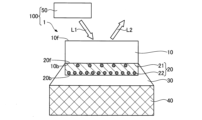
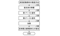
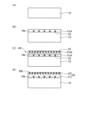
- FIG. 2 is an explanatory diagram schematically showing a cross-sectional configuration of a wavelength conversion member. It is a flowchart of the manufacturing method of a wavelength conversion member. It is an explanatory view showing a manufacturing process of a wavelength conversion member.
- FIG. 1 is an explanatory diagram schematically showing a cross-sectional configuration of a wavelength conversion member 1 according to an embodiment of the present invention.
- the wavelength conversion member 1 converts excitation light L1 emitted from a light source 50 such as a light emitting diode (LED) or a laser diode (LD) into fluorescence L2 having a different wavelength from the light L1. It is a member that emits light.
- the wavelength conversion member 1 is used, for example, in various optical devices such as headlamps, lighting, and projectors.
- the wavelength conversion member 1 shown in FIG. 1 is part of a light source device 100.
- the light source device 100 includes, in addition to the wavelength conversion member 1, a light source 50 that emits excitation light L1.
- the wavelength conversion member 1 includes a phosphor 10, a reflective film 20, a bonding layer 30, and a heat dissipation member 40.
- the phosphor 10 emits fluorescence L2 by the irradiated excitation light L1.
- the phosphor 10 has an entrance surface 10f and a back surface 10b.
- the entrance surface 10f is a surface on which the excitation light L1 enters.
- the back surface 10b is a surface located on the opposite side of the incident surface 10f.
- the ceramic sintered body constituting the phosphor 10 includes a fluorescent phase mainly composed of crystal grains having fluorescence and a transparent phase mainly composed of crystal grains having translucency.
- the crystal particles of the transparent phase are Al 2 O 3 (alumina).
- the crystal particles of the fluorescent phase preferably have a composition represented by A 3 B 5 O 12 :Ce (so-called garnet structure). "A 3 B 5 O 12 :Ce" indicates that Ce is dissolved in A 3 B 5 O 12 and a part of element A is replaced with Ce.
- a 3 B 5 O 12 :Element A and element B in Ce are each composed of at least one type of element selected from the following element group.
- Element A Lanthanoids excluding Sc, Y, and Ce (however, element A may further contain Gd)
- Element B Al (however, it may further contain Gd as element B)
- the reflective film 20 is disposed on the side of the back surface 10b of the phosphor 10, and reflects the excitation light L1 incident on the phosphor 10 that has passed through the phosphor 10, and the back surface of the fluorescence L2 emitted from the phosphor 10.
- the fluorescent light directed toward the phosphor 10b is reflected toward the phosphor 10.
- the reflective film 20 has a first surface 20f and a second surface 20b.
- the first surface 20f is a surface facing the back surface 10b of the phosphor 10.
- the second surface 20b is a surface located on the opposite side of the first surface 20f.
- the reflective film 20 is composed of a metal layer 21 and particles 22.
- the metal constituting the metal layer 21 include silver (Ag), platinum (Pt), aluminum (Al), and a silver alloy.
- the metal constituting the metal layer 21 is silver (Ag). be.
- Particles 22 are contained within metal layer 21 .
- the particles 22 include ceramic particles such as Al2O3 , YAG, TiO2 , Y2O3 , SiO2 , Cr2O3 , Nb2O5 , Ta2O5 , Ni, W , Mo, Cr , Examples include metal particles such as Nb, and in this embodiment, the particles 22 are Al 2 O 3 .
- the material constituting the particles 22 is Al 2 O 3 similar to the crystal grains of the transparent phase of the phosphor 10 , the material constituting the particles 22 does not include the material contained in the phosphor 10 .
- the proportion of the volume occupied by the particles 22 in the reflective film 20 is preferably 0.1 to 20.0% of the volume occupied by the metal layer 21.
- the thickness is preferably 1 to 100 ⁇ m, and the particle diameter of the particles 22 is 0.
- the thickness is preferably 5 to 50 ⁇ m.
- the particle diameter of the particles 22 is less than half the thickness of the reflective film 20. Note that the average value of the particle diameters of arbitrary 100 particles 22 among the particles 22 observed in a cross-sectional image by a scanning electron microscope (SEM) is used as the value of the particle diameter.
- the melting point of the particles 22 is higher than the melting point of the metal constituting the metal layer 21.
- the melting point of Al 2 O 3 constituting the particles 22 of this embodiment is 2072°C
- the melting point of silver (Ag) constituting the metal layer 21 is 961.8°C.
- the specific gravity of the particles 22 is smaller than the specific gravity of the metal layer 21.
- more particles 22 are contained on the second surface 20b side than on the first surface 20f side.
- a distribution of particles 22 is confirmed by analyzing a cross-sectional image taken by a scanning electron microscope (SEM).
- SEM scanning electron microscope
- the distribution of the particles 22 is similar to the distribution of the particles 22 in the vicinity of the first surface 20f in a cross-sectional image (for example, a cross-section as shown in FIG. 1) perpendicular to the incident surface 10f of the phosphor 10. , and the distribution of the particles 22 in the vicinity of the second surface 20b.
- the distribution of particles 22 in the vicinity of this first surface 20f ranges from the first surface 20f to a depth of 10% of the thickness of the reflective film 20 (the length between the first surface 20f and the second surface 20b). It is expressed as the value obtained by dividing the cross-sectional area of the particles 22 existing within the range by the cross-sectional area of the metal layer 21 existing within the same range.
- the distribution of the particles 22 in the vicinity of the second surface 20b similarly has the cross-sectional area of the particles 22 existing within the range from the second surface 20b to a depth of 10% of the thickness of the reflective film 20 within the same range. It is expressed as a value divided by the cross-sectional area of the metal layer 21 existing within. Note that FIG.
- 1 is a diagram schematically showing the distribution of particles 22 in the reflective film 20, and the particles 22 included on the first surface 20f side and the particles 22 included on the second surface 20b side are as follows.
- the particles 22 may not be distributed at equal intervals, and the particles 22 may also be included in a portion of the reflective film 20 closer to the center between the first surface 20f and the second surface 20b.
- the ratio of the particles 22 included on the first surface 20f side to the particles 22 included on the second surface 20b side does not have to be the ratio shown in FIG. 1.
- the bonding layer 30 is disposed between the reflective film 20 and a heat radiating member 40, which will be described later, and joins the reflective film 20 and the heat radiating member 40.
- the bonding layer 30 is made of AuSn solder containing gold (Au) and tin (Sn). Note that the bonding layer 30 is not limited to AuSn solder, and may also be formed using solders such as Sn-Pb solder, Sn-Ag-Cu solder, Sn-Zn-Bi solder, Sn-Cu solder, and Sn-Ag-In-Bi solder. good. Alternatively, it may be formed by sintering fine powder of silver (Ag), copper (Cu), or the like.
- the heat dissipation member 40 is arranged on the second surface 20b side of the reflective film 20 and dissipates the heat generated by the phosphor 10 to the outside of the wavelength conversion member 1.
- the heat dissipation member 40 is arranged on the surface of the bonding layer 30 that is located on the opposite side of the surface bonded to the reflective film 20.
- the material constituting the heat dissipation member 40 include materials having higher thermal conductivity than the phosphor 10, such as copper, copper-molybdenum alloy, copper-tungsten alloy, and aluminum; in this embodiment, the material constituting the heat dissipation member 40 is copper.
- FIG. 2 is a flowchart of the method for manufacturing the wavelength conversion member 1.
- FIGS. 3A to 3D are explanatory diagrams showing the manufacturing process of the wavelength conversion member 1.
- the phosphor 10 is prepared (step S10).
- the phosphor 10 is made into a clay made by drying and granulating a slurry of pulverized and mixed materials of the fluorescent phase and the transparent phase and ethanol, and further adding a binder and water and kneading the slurry. It is prepared by firing a molded article made from the clay.
- FIG. 10 is prepared (step S10).
- the phosphor 10 is made into a clay made by drying and granulating a slurry of pulverized and mixed materials of the fluorescent phase and the transparent phase and ethanol, and further adding a binder and water and kneading the slurry. It is prepared by firing a molded article made from the clay.
- a first paste 21pf is applied to the back surface 10b of the phosphor 10 (step S20). Specifically, with the back surface 10b of the phosphor 10 facing upward in the direction of gravity, the first paste 21pf is applied onto the back surface 10b.
- the first paste 21pf is prepared in advance by mixing metal powder and particles 22 constituting the metal layer 21 with an acrylic binder and a solvent.
- the second paste 21pb is applied to the surface of the first paste 21pf that is opposite to the back surface 10b (step S30).
- the second paste 21pb is the same as the first paste 21pf except that it contains more particles 22 than the first paste 21pf.
- the laminate LM is a laminate in which the phosphor 10, the first paste 21pf, and the second paste 21pb are laminated.
- the laminate LM is heated at a temperature higher than the melting point of the metal contained in the first and second pastes 21pf and 21pb and lower than the melting point of the particles 22, so that the first paste 21pf and the second paste 21pb are fused. As shown in FIG.
- a reflective film 20 is formed on the back surface 10b of the phosphor 10 (step S40). Note that when the first paste 21pf and the second paste 21pb are fused, the specific gravity of the particles 22 contained in each paste is smaller than the specific gravity of the metal contained in the same paste, so that the particles 22 contained in the first paste 21pf are Some of the particles 22 move to the second paste 21pb side (not shown in FIG. 3(D)). The amount of movement of the particles 22 is adjusted by the heating temperature and heating time. Then, the method for manufacturing the wavelength conversion member 1 is completed by bonding the reflective film 20 and the heat dissipating member 40 via the bonding layer 30 (step S50).
- the melting point of the particles 22 is higher than the melting point of the metal constituting the metal layer 21, and such particles 22 are Also included in a large amount on the second surface 20b side.
- the base material of the reflective film 20 including the metal constituting the metal layer 21 and the particles 22 is used.
- the metal constituting the metal layer 21 is melted.
- the reflective film 20 can be formed on the back surface 10b of the phosphor 10 while increasing the adhesion of the metal layer 21 to the phosphor 10. Therefore, the bonding strength between the phosphor 10 and the reflective film 20 can be increased. Further, when forming the reflective film 20 on the back surface 10b of the phosphor 10, the particles 22 included on the second surface 20b side are not melted and are larger than on the first surface 20f side. Therefore, the surface tension that acts on each particle 22 and the molten metal conflicts with the surface tension that acts on the phosphor 10 and the molten metal, so the force of the metal to aggregate with respect to the phosphor 10 is weakened, and the molten metal layer 21 can be suppressed from aggregating.
- the reflective film 20 can be easily spread along the phosphor 10, the bonding strength between the phosphor 10 and the reflective film 20 can be increased from this point of view as well. Further, when forming the reflective film 20 on the back surface 10b of the phosphor 10, the particles 22 included on the first surface 20f side are not melted like the particles 22 included on the second surface 20b side. It is smaller than that on the second surface 20b side. Therefore, the molten particles 22 and the back surface 10b of the phosphor 10 may react, and many particles 22 may gather on the first surface 20f side, reducing the area of the metal layer 21 exposed on the first surface 20f. It is possible to suppress a decrease in the reflectance of the reflective film 20 that occurs in this case.
- the wavelength conversion member 1 of the present embodiment it is possible to provide a wavelength conversion member 1 in which the bonding strength between the phosphor 10 and the reflective film 20 is increased, and a decrease in the reflectance of the reflective film 20 is suppressed. .
- the particles 22 are Al 2 O 3 . Since Al 2 O 3 has high light transmittance, it can prevent the particles 22 from absorbing excitation light and fluorescence that have reached the reflective film 20 side, and therefore it can suppress a decrease in the reflectance of the reflective film 20.
- the specific gravity of the particles 22 is smaller than the specific gravity of the metal layer 21, so the particles 22 are It can be made unevenly distributed on the upper side in the direction of gravity. For this reason, when forming the reflective film 20 on the back surface 10b of the phosphor 10, the heated metal layer 21 and particles 22 are formed as the reflective film 20 on the back surface 10b of the phosphor 10 facing upward in the direction of gravity. By doing so (see FIG. 3), the particles 22 can be easily distributed on the second surface 20b side. As a result, it is possible to accurately provide the wavelength conversion member 1 in which more particles 22 are contained on the second surface 20b side than on the first surface 20f side.
- the particle diameter of the particles 22 is less than half the thickness of the reflective film 20.
- the proportion of the thickness occupied by the metal layer 21 in the thickness of the reflective film 20 becomes relatively small, and the possibility that through holes will be formed in the metal layer 21 increases.
- the reflective film 20 there is a high possibility that a portion without the metal layer 21 will be formed when viewed from above. Therefore, in the wavelength conversion member 1, the possibility that a through hole is formed in the metal layer 21 can be reduced, and a reduction in the reflective performance of the reflective film can be suppressed.
- the material forming the particles 22 includes the material contained in the phosphor 10. Therefore, the difference between the coefficient of thermal expansion of the particles 22 and the coefficient of thermal expansion of the phosphor 10 can be reduced. Therefore, since the temperature range in which the particles 22 do not expand excessively and the temperature range in which the phosphor 10 does not expand excessively overlaps widely, the heating during the manufacture of the wavelength conversion member 1 and the incoming excitation light L1 In heating by thermal conversion, it is possible to set a wide allowable temperature range in which the particles 22 and the phosphor 10 are not thermally expanded excessively.
- the wavelength conversion member 1 of this embodiment includes a heat radiating member 40 that radiates heat generated by the phosphor 10 to the outside. Therefore, the heat generated by converting a part of the excitation light L1 incident on the phosphor 10 can be radiated to the outside of the wavelength conversion member 1 by the heat radiating member 40. Thereby, it is possible to suppress thermal quenching in which the amount of fluorescence from the phosphor 10 decreases due to an increase in temperature. Therefore, a decrease in the amount of fluorescence emitted from the phosphor 10 can be suppressed.
- the excitation light L1 irradiated from the light source 50 to the phosphor 10 is emitted from the phosphor 10 as fluorescence L2.
- the reflection film 20 contains more particles on the second surface 20b side than on the first surface 20f side, thereby suppressing a decrease in reflectance. Therefore, the intensity of the excitation light L1 incident on the phosphor 10 that has passed through the phosphor 10 and the fluorescence L2 emitted from the phosphor 10 directed toward the back surface are reduced. The excitation light and fluorescence can be reflected toward the phosphor 10 while being suppressed.
- the bonding strength between the phosphor 10 and the reflective film 20 is increased. It is elevated.
- the reflective film 20 is placed in direct contact with the back surface 10b of the phosphor 10, as shown in FIG. 1, but the invention is not limited thereto.
- other configurations may be arranged between the reflective film 20 and the phosphor 10.
- Other configurations include an adhesion film and an increased reflection film. Even when such a structure is disposed between the reflective film 20 and the phosphor 10, it is possible to form the reflective film 20 with enhanced adhesion to the structure and the phosphor 10. can.
- the particles 22 are not limited to Al 2 O 3 .
- the particles 22 may be YAG.
- the particles 22 made of YAG are included in the reflective film 20, it is possible to absorb the blue light contained in the excitation light or fluorescence that has reached the reflective film 20 side, and emit yellow light.
- the material constituting the particles 22 was Al 2 O 3 similar to the crystal particles of the transparent phase of the phosphor 10, but the material is not limited thereto.
- the material constituting the particles 22 only needs to contain at least a part of the materials contained in the phosphor 10, and may further contain a different material from the material contained in the phosphor 10.
- the material constituting the particles 22 has a coefficient of thermal expansion equivalent to that of the material included in the phosphor 10. It is preferable that the material has the following properties.
- the particles 22 are made of Al 2 O 3 and the metal layer 21 is made of silver (Ag), but the present invention is not limited thereto.
- the particles 22 and the metal layer 21 may each be made of a plurality of materials.
- the melting point of the particles 22 is higher than the melting point of the metal constituting the metal layer 21, which means that the melting point of the material having the lowest melting point among the materials constituting the particles 22 constitutes the metal layer 21. This means that it is higher than the melting point of the material with the highest melting point among the multiple materials.
- the reflective film 20 is formed from two types of pastes (first and second pastes 21pf and 21pb) having different particle contents, but the invention is not limited to this.
- the reflective film 20 may be formed from one type of paste, or may be formed from three or more types of paste, as long as the paste contains the metal constituting the metal layer 21 and particles 22 whose specific gravity is smaller than that metal.
- the film may be formed from.
- a wavelength conversion member a phosphor that emits fluorescence in response to excitation light, the phosphor having an incident surface on which the excitation light enters and a back surface located on the opposite side of the incident surface; a reflective film disposed on the back surface side of the phosphor and composed of a metal layer and particles contained inside the metal layer; The melting point of the particles is higher than the melting point of the metal constituting the metal layer, The reflective film is a first surface facing the back surface of the phosphor; a second surface located on the opposite side of the first surface, A wavelength conversion member, wherein the particles are contained more on the second surface side than on the first surface side.
- a wavelength conversion member according to any one of Application Examples 1 to 4, further comprising: A wavelength conversion member comprising a heat radiating member disposed on the second surface side of the reflective film and radiating heat generated by the phosphor to the outside.
- a light source device The wavelength conversion member according to any one of Application Examples 1 to 5; A light source device comprising: a light source that irradiates the excitation light onto the incident surface.
Landscapes
- Physics & Mathematics (AREA)
- Engineering & Computer Science (AREA)
- General Engineering & Computer Science (AREA)
- Spectroscopy & Molecular Physics (AREA)
- Optics & Photonics (AREA)
- General Physics & Mathematics (AREA)
- Microelectronics & Electronic Packaging (AREA)
- Optical Filters (AREA)
- Luminescent Compositions (AREA)
- Optical Elements Other Than Lenses (AREA)
- Mounting And Adjusting Of Optical Elements (AREA)
- Cooling Or The Like Of Electrical Apparatus (AREA)
- Projection Apparatus (AREA)
Abstract
Description
この構成によれば、波長変換部材の製造時に溶融している金属層の内部において、粒子を重力方向上側に偏在しやすくすることができる。このため、蛍光体の裏面に反射膜を成膜する際、重力方向上側を向いた蛍光体の裏面に対して加熱した金属層および粒子を反射膜として成膜することにより、粒子を第2面の側に偏在しやすくすることができる。したがって、第1面の側よりも第2面の側に粒子が多く含まれている波長変換部材を精度良く提供することができる。
粒子の粒子径が大きくなると、反射膜の厚さのうち金属層が占める厚さの割合が相対的に小さくなり、金属層に貫通孔が形成される可能性が高くなる。つまり反射膜において、上面視で金属層が無い部分が形成される可能性が高くなる。この構成によれば、金属層に貫通孔が形成される可能性を低減することができ、反射膜の反射性能の低減を抑制することができる。
この構成によれば、粒子の熱膨張率と蛍光体の熱膨張率との差を小さくできる。したがって、粒子が過度に熱膨張しない温度帯域と蛍光体が過度に熱膨張しない温度帯域とは広く重複していることから、波長変換部材の製造時の加熱や入射した励起光の熱変換による加熱において、粒子および蛍光体を過度に熱膨張させない許容温度帯域を広く設定することができる。すなわち、この構成によれば、クラックや変形、蛍光体と反射膜との剥離等の、蛍光体や粒子の過度な熱膨張によって生じる不具合を生じにくくすることができる。また、蛍光体と粒子とが接触している界面での反応による組成変化を抑制することもできる。
この構成によれば、蛍光体に入射した励起光の一部が変換されて生じる熱を、放熱部材により波長変換部材の外部に放熱することができる。これにより、温度上昇したことで蛍光体からの蛍光量が低下する熱消光を抑制することができる。したがって、蛍光体から発せられる蛍光量の低下を抑制することができる。
この構成によれば、光源から蛍光体に照射された励起光は、蛍光体から蛍光として発せられる。また、反射膜は、第1面の側よりも第2面の側に粒子が多く含まれていることで反射率の低下が抑制されている。このため、蛍光体に入射した励起光のうち蛍光体を透過した励起光と、蛍光体から発せられた蛍光のうち裏面の側に向かった蛍光と、の各々の強度低下を抑制しつつ、それら励起光および蛍光を蛍光体の側に反射させることができる。また、このような反射膜を備えていることにより、反射膜の反射率の低下が抑制されていることに加えて、蛍光体と反射膜との接合強度が高められた光源装置を提供することができる。
元素A:Sc、Y、Ceを除くランタノイド(ただし、元素AとしてさらにGdを含んでいてもよい)
元素B:Al(ただし、元素BとしてさらにGdを含んでいてもよい)
蛍光体10として、セラミック焼結体を採用することで、蛍光相と透光相との界面で光が散乱し、光の色の角度依存性を減らすことができる。これにより、色の均質性を向上することができる。なお、蛍光体10の材料は、上述の材料に限定されない。
本発明は上記の実施形態に限られるものではなく、その要旨を逸脱しない範囲において種々の態様において実施することが可能であり、例えば次のような変形も可能である。
[適用例1]
波長変換部材であって、
励起光によって蛍光を発する蛍光体であって、前記励起光が入射する入射面および前記入射面の反対側に位置する裏面を有する蛍光体と、
前記蛍光体の前記裏面の側に配置され、金属層および前記金属層の内部に含まれる粒子から構成された反射膜と、を備え、
前記粒子の融点は、前記金属層を構成する金属の融点よりも高く、
前記反射膜は、
前記蛍光体の前記裏面と対向する第1面と、
前記第1面の反対側に位置する第2面と、を有し、
前記粒子は、前記第1面の側よりも前記第2面の側に多く含まれていることを特徴とする、波長変換部材。
[適用例2]
適用例1に記載の波長変換部材であって、
前記粒子の比重は、前記金属層の比重よりも小さいことを特徴とする、波長変換部材。
[適用例3]
適用例1または適用例2に記載の波長変換部材であって、
前記第1面と前記第2面との間の長さを前記反射膜の厚さとしたとき、前記粒子の粒子径は、前記反射膜の厚さの半分以下であることを特徴とする、波長変換部材。
[適用例4]
適用例1から適用例3までのいずれかに記載の波長変換部材であって、
前記粒子を構成する材料は、前記蛍光体に含まれる材料を含むことを特徴とする、波長変換部材。
[適用例5]
適用例1から適用例4までのいずれかに記載の波長変換部材であって、さらに、
前記反射膜の前記第2面の側に配置され、前記蛍光体で発生する熱を外部に放熱する放熱部材を備えることを特徴とする、波長変換部材。
[適用例6]
光源装置であって、
適用例1から適用例5までのいずれかに記載の波長変換部材と、
前記入射面に前記励起光を照射する光源と、を備えることを特徴とする、光源装置。
10…蛍光体
10f…入射面
10b…裏面
20…反射膜
20f…第1面
20b…第2面
21…金属層
21pf…第1ペースト
21pb…第2ペースト
22…粒子
30…接合層
40…放熱部材
50…光源
100…光源装置
Claims (6)
- 波長変換部材であって、
励起光によって蛍光を発する蛍光体であって、前記励起光が入射する入射面および前記入射面の反対側に位置する裏面を有する蛍光体と、
前記蛍光体の前記裏面の側に配置され、金属層および前記金属層の内部に含まれる粒子から構成された反射膜と、を備え、
前記粒子の融点は、前記金属層を構成する金属の融点よりも高く、
前記反射膜は、
前記蛍光体の前記裏面と対向する第1面と、
前記第1面の反対側に位置する第2面と、を有し、
前記粒子は、前記第1面の側よりも前記第2面の側に多く含まれていることを特徴とする、波長変換部材。 - 請求項1に記載の波長変換部材であって、
前記粒子の比重は、前記金属層の比重よりも小さいことを特徴とする、波長変換部材。 - 請求項2に記載の波長変換部材であって、
前記第1面と前記第2面との間の長さを前記反射膜の厚さとしたとき、前記粒子の粒子径は、前記反射膜の厚さの半分以下であることを特徴とする、波長変換部材。 - 請求項3に記載の波長変換部材であって、
前記粒子を構成する材料は、前記蛍光体に含まれる材料を含むことを特徴とする、波長変換部材。 - 請求項4に記載の波長変換部材であって、さらに、
前記反射膜の前記第2面の側に配置され、前記蛍光体で発生する熱を外部に放熱する放熱部材を備えることを特徴とする、波長変換部材。 - 光源装置であって、
請求項1から請求項5までのいずれか一項に記載の波長変換部材と、
前記入射面に前記励起光を照射する光源と、を備えることを特徴とする、光源装置。
Priority Applications (3)
| Application Number | Priority Date | Filing Date | Title |
|---|---|---|---|
| KR1020247036070A KR20240166022A (ko) | 2022-05-13 | 2023-04-26 | 파장 변환 부재 및 광원 장치 |
| EP23803443.3A EP4524624A4 (en) | 2022-05-13 | 2023-04-26 | WAVELENGTH CONVERSION ELEMENT AND LIGHT SOURCE DEVICE |
| CN202380037290.4A CN119234165A (zh) | 2022-05-13 | 2023-04-26 | 波长转换构件和光源装置 |
Applications Claiming Priority (2)
| Application Number | Priority Date | Filing Date | Title |
|---|---|---|---|
| JP2022079229A JP7721481B2 (ja) | 2022-05-13 | 2022-05-13 | 波長変換部材および光源装置 |
| JP2022-079229 | 2022-05-13 |
Publications (1)
| Publication Number | Publication Date |
|---|---|
| WO2023218964A1 true WO2023218964A1 (ja) | 2023-11-16 |
Family
ID=88730408
Family Applications (1)
| Application Number | Title | Priority Date | Filing Date |
|---|---|---|---|
| PCT/JP2023/016466 Ceased WO2023218964A1 (ja) | 2022-05-13 | 2023-04-26 | 波長変換部材および光源装置 |
Country Status (6)
| Country | Link |
|---|---|
| EP (1) | EP4524624A4 (ja) |
| JP (1) | JP7721481B2 (ja) |
| KR (1) | KR20240166022A (ja) |
| CN (1) | CN119234165A (ja) |
| TW (1) | TW202409616A (ja) |
| WO (1) | WO2023218964A1 (ja) |
Cited By (1)
| Publication number | Priority date | Publication date | Assignee | Title |
|---|---|---|---|---|
| WO2025205324A1 (ja) * | 2024-03-28 | 2025-10-02 | パナソニックIpマネジメント株式会社 | 波長変換部材、蛍光体デバイス及び波長変換部材の製造方法 |
Citations (8)
| Publication number | Priority date | Publication date | Assignee | Title |
|---|---|---|---|---|
| JP2011530789A (ja) * | 2008-08-08 | 2011-12-22 | シカト・インコーポレイテッド | 色調節可能な光源 |
| JP2012190628A (ja) * | 2011-03-10 | 2012-10-04 | Stanley Electric Co Ltd | 光源装置および照明装置 |
| JP2017224667A (ja) * | 2016-06-14 | 2017-12-21 | 日亜化学工業株式会社 | 光透過部材の製造方法及び発光装置の製造方法 |
| WO2018042826A1 (ja) * | 2016-08-30 | 2018-03-08 | パナソニックIpマネジメント株式会社 | 色変換素子及び照明装置 |
| JP2019053130A (ja) * | 2017-09-13 | 2019-04-04 | 日亜化学工業株式会社 | 光学部品、光学部品を用いた発光装置、及び光学部品の製造方法 |
| JP2019525232A (ja) * | 2016-07-13 | 2019-09-05 | 深▲せん▼光峰科技股▲分▼有限公司Appotronics Corporation Limited | 波長変換装置およびその製造方法 |
| JP2019159175A (ja) * | 2018-03-15 | 2019-09-19 | 日本特殊陶業株式会社 | 光波長変換部材及び光波長変換装置 |
| WO2020211091A1 (en) * | 2019-04-19 | 2020-10-22 | Materion Precision Optics (Shanghai) Limited | High temperature resistant reflective layer for wavelength conversion devices |
Family Cites Families (2)
| Publication number | Priority date | Publication date | Assignee | Title |
|---|---|---|---|---|
| DE102013013296B4 (de) | 2013-08-12 | 2020-08-06 | Schott Ag | Konverter-Kühlkörperverbund mit metallischer Lotverbindung und Verfahren zu dessen Herstellung |
| DE102017104130A1 (de) * | 2017-02-28 | 2018-08-30 | Osram Gmbh | Anorganische Reflexionsbeschichtung, optoelektronisches Bauelement und Verfahren zur Herstellung eines optoelektronischen Bauelements |
-
2022
- 2022-05-13 JP JP2022079229A patent/JP7721481B2/ja active Active
-
2023
- 2023-04-26 CN CN202380037290.4A patent/CN119234165A/zh active Pending
- 2023-04-26 EP EP23803443.3A patent/EP4524624A4/en active Pending
- 2023-04-26 WO PCT/JP2023/016466 patent/WO2023218964A1/ja not_active Ceased
- 2023-04-26 KR KR1020247036070A patent/KR20240166022A/ko active Pending
- 2023-05-11 TW TW112117478A patent/TW202409616A/zh unknown
Patent Citations (8)
| Publication number | Priority date | Publication date | Assignee | Title |
|---|---|---|---|---|
| JP2011530789A (ja) * | 2008-08-08 | 2011-12-22 | シカト・インコーポレイテッド | 色調節可能な光源 |
| JP2012190628A (ja) * | 2011-03-10 | 2012-10-04 | Stanley Electric Co Ltd | 光源装置および照明装置 |
| JP2017224667A (ja) * | 2016-06-14 | 2017-12-21 | 日亜化学工業株式会社 | 光透過部材の製造方法及び発光装置の製造方法 |
| JP2019525232A (ja) * | 2016-07-13 | 2019-09-05 | 深▲せん▼光峰科技股▲分▼有限公司Appotronics Corporation Limited | 波長変換装置およびその製造方法 |
| WO2018042826A1 (ja) * | 2016-08-30 | 2018-03-08 | パナソニックIpマネジメント株式会社 | 色変換素子及び照明装置 |
| JP2019053130A (ja) * | 2017-09-13 | 2019-04-04 | 日亜化学工業株式会社 | 光学部品、光学部品を用いた発光装置、及び光学部品の製造方法 |
| JP2019159175A (ja) * | 2018-03-15 | 2019-09-19 | 日本特殊陶業株式会社 | 光波長変換部材及び光波長変換装置 |
| WO2020211091A1 (en) * | 2019-04-19 | 2020-10-22 | Materion Precision Optics (Shanghai) Limited | High temperature resistant reflective layer for wavelength conversion devices |
Non-Patent Citations (1)
| Title |
|---|
| See also references of EP4524624A4 |
Cited By (1)
| Publication number | Priority date | Publication date | Assignee | Title |
|---|---|---|---|---|
| WO2025205324A1 (ja) * | 2024-03-28 | 2025-10-02 | パナソニックIpマネジメント株式会社 | 波長変換部材、蛍光体デバイス及び波長変換部材の製造方法 |
Also Published As
| Publication number | Publication date |
|---|---|
| JP7721481B2 (ja) | 2025-08-12 |
| EP4524624A4 (en) | 2026-04-22 |
| JP2023167773A (ja) | 2023-11-24 |
| EP4524624A1 (en) | 2025-03-19 |
| KR20240166022A (ko) | 2024-11-25 |
| TW202409616A (zh) | 2024-03-01 |
| CN119234165A (zh) | 2024-12-31 |
Similar Documents
| Publication | Publication Date | Title |
|---|---|---|
| JP6320531B2 (ja) | 金属はんだ接合部を有するコンバーター・冷却体複合体 | |
| JP6845372B2 (ja) | 光波長変換装置 | |
| KR20200042933A (ko) | 광파장 변환 장치 및 광복합 장치 | |
| JP2014137973A (ja) | 光源装置 | |
| US11994284B2 (en) | Wavelength conversion member and light source device provided therewith | |
| JP7721481B2 (ja) | 波長変換部材および光源装置 | |
| JP7244297B2 (ja) | 光波長変換部品 | |
| JP7387898B2 (ja) | 蛍光板、波長変換部材、および、光源装置 | |
| JP2019207761A (ja) | 光波長変換装置 | |
| CN114041073B (zh) | 波长转换构件、光源装置和波长转换构件的制造方法 | |
| CN114096782B (zh) | 钎焊用波长转换构件、波长转换装置和光源装置 | |
| TWI802898B (zh) | 螢光板、波長轉換構件及光源裝置 | |
| JP7821039B2 (ja) | 波長変換部材および光源装置 | |
| CN115003957B (zh) | 荧光板、波长转换构件和光源装置 | |
| JP2024013799A (ja) | 波長変換部材、波長変換装置、および、光源装置 | |
| JP2019197143A (ja) | 光波長変換装置 | |
| JP2024099928A (ja) | 波長変換部材、波長変換装置、および、光源装置 |
Legal Events
| Date | Code | Title | Description |
|---|---|---|---|
| 121 | Ep: the epo has been informed by wipo that ep was designated in this application |
Ref document number: 23803443 Country of ref document: EP Kind code of ref document: A1 |
|
| ENP | Entry into the national phase |
Ref document number: 20247036070 Country of ref document: KR Kind code of ref document: A |
|
| WWE | Wipo information: entry into national phase |
Ref document number: 202380037290.4 Country of ref document: CN |
|
| WWE | Wipo information: entry into national phase |
Ref document number: 2023803443 Country of ref document: EP |
|
| NENP | Non-entry into the national phase |
Ref country code: DE |
|
| ENP | Entry into the national phase |
Ref document number: 2023803443 Country of ref document: EP Effective date: 20241213 |
|
| WWP | Wipo information: published in national office |
Ref document number: 202380037290.4 Country of ref document: CN |