WO2023224005A1 - 太陽電池モジュールおよび太陽電池モジュールの製造方法 - Google Patents
太陽電池モジュールおよび太陽電池モジュールの製造方法 Download PDFInfo
- Publication number
- WO2023224005A1 WO2023224005A1 PCT/JP2023/018128 JP2023018128W WO2023224005A1 WO 2023224005 A1 WO2023224005 A1 WO 2023224005A1 JP 2023018128 W JP2023018128 W JP 2023018128W WO 2023224005 A1 WO2023224005 A1 WO 2023224005A1
- Authority
- WO
- WIPO (PCT)
- Prior art keywords
- layer
- electrode layer
- substrate
- transparent conductive
- solar cell
- Prior art date
- Legal status (The legal status is an assumption and is not a legal conclusion. Google has not performed a legal analysis and makes no representation as to the accuracy of the status listed.)
- Ceased
Links
Images

Classifications
-
- H—ELECTRICITY
- H10—SEMICONDUCTOR DEVICES; ELECTRIC SOLID-STATE DEVICES NOT OTHERWISE PROVIDED FOR
- H10K—ORGANIC ELECTRIC SOLID-STATE DEVICES
- H10K30/00—Organic devices sensitive to infrared radiation, light, electromagnetic radiation of shorter wavelength or corpuscular radiation
- H10K30/80—Constructional details
- H10K30/89—Terminals, e.g. bond pads
-
- H—ELECTRICITY
- H02—GENERATION; CONVERSION OR DISTRIBUTION OF ELECTRIC POWER
- H02S—GENERATION OF ELECTRIC POWER BY CONVERSION OF INFRARED RADIATION, VISIBLE LIGHT OR ULTRAVIOLET LIGHT, e.g. USING PHOTOVOLTAIC [PV] MODULES
- H02S40/00—Components or accessories in combination with PV modules, not provided for in groups H02S10/00 - H02S30/00
- H02S40/30—Electrical components
- H02S40/34—Electrical components comprising specially adapted electrical connection means to be structurally associated with the PV module, e.g. junction boxes
-
- H—ELECTRICITY
- H10—SEMICONDUCTOR DEVICES; ELECTRIC SOLID-STATE DEVICES NOT OTHERWISE PROVIDED FOR
- H10F—INORGANIC SEMICONDUCTOR DEVICES SENSITIVE TO INFRARED RADIATION, LIGHT, ELECTROMAGNETIC RADIATION OF SHORTER WAVELENGTH OR CORPUSCULAR RADIATION
- H10F19/00—Integrated devices, or assemblies of multiple devices, comprising at least one photovoltaic cell covered by group H10F10/00, e.g. photovoltaic modules
- H10F19/30—Integrated devices, or assemblies of multiple devices, comprising at least one photovoltaic cell covered by group H10F10/00, e.g. photovoltaic modules comprising thin-film photovoltaic cells
- H10F19/31—Integrated devices, or assemblies of multiple devices, comprising at least one photovoltaic cell covered by group H10F10/00, e.g. photovoltaic modules comprising thin-film photovoltaic cells having multiple laterally adjacent thin-film photovoltaic cells deposited on the same substrate
- H10F19/35—Structures for the connecting of adjacent photovoltaic cells, e.g. interconnections or insulating spacers
-
- H—ELECTRICITY
- H10—SEMICONDUCTOR DEVICES; ELECTRIC SOLID-STATE DEVICES NOT OTHERWISE PROVIDED FOR
- H10K—ORGANIC ELECTRIC SOLID-STATE DEVICES
- H10K30/00—Organic devices sensitive to infrared radiation, light, electromagnetic radiation of shorter wavelength or corpuscular radiation
- H10K30/80—Constructional details
- H10K30/88—Passivation; Containers; Encapsulations
-
- H—ELECTRICITY
- H10—SEMICONDUCTOR DEVICES; ELECTRIC SOLID-STATE DEVICES NOT OTHERWISE PROVIDED FOR
- H10K—ORGANIC ELECTRIC SOLID-STATE DEVICES
- H10K39/00—Integrated devices, or assemblies of multiple devices, comprising at least one organic radiation-sensitive element covered by group H10K30/00
- H10K39/10—Organic photovoltaic [PV] modules; Arrays of single organic PV cells
- H10K39/12—Electrical configurations of PV cells, e.g. series connections or parallel connections
-
- H—ELECTRICITY
- H10—SEMICONDUCTOR DEVICES; ELECTRIC SOLID-STATE DEVICES NOT OTHERWISE PROVIDED FOR
- H10K—ORGANIC ELECTRIC SOLID-STATE DEVICES
- H10K39/00—Integrated devices, or assemblies of multiple devices, comprising at least one organic radiation-sensitive element covered by group H10K30/00
- H10K39/10—Organic photovoltaic [PV] modules; Arrays of single organic PV cells
- H10K39/18—Interconnections, e.g. terminals
-
- H—ELECTRICITY
- H10—SEMICONDUCTOR DEVICES; ELECTRIC SOLID-STATE DEVICES NOT OTHERWISE PROVIDED FOR
- H10K—ORGANIC ELECTRIC SOLID-STATE DEVICES
- H10K30/00—Organic devices sensitive to infrared radiation, light, electromagnetic radiation of shorter wavelength or corpuscular radiation
- H10K30/40—Organic devices sensitive to infrared radiation, light, electromagnetic radiation of shorter wavelength or corpuscular radiation comprising a p-i-n structure, e.g. having a perovskite absorber between p-type and n-type charge transport layers
-
- H—ELECTRICITY
- H10—SEMICONDUCTOR DEVICES; ELECTRIC SOLID-STATE DEVICES NOT OTHERWISE PROVIDED FOR
- H10K—ORGANIC ELECTRIC SOLID-STATE DEVICES
- H10K30/00—Organic devices sensitive to infrared radiation, light, electromagnetic radiation of shorter wavelength or corpuscular radiation
- H10K30/50—Photovoltaic [PV] devices
-
- H—ELECTRICITY
- H10—SEMICONDUCTOR DEVICES; ELECTRIC SOLID-STATE DEVICES NOT OTHERWISE PROVIDED FOR
- H10K—ORGANIC ELECTRIC SOLID-STATE DEVICES
- H10K30/00—Organic devices sensitive to infrared radiation, light, electromagnetic radiation of shorter wavelength or corpuscular radiation
- H10K30/80—Constructional details
- H10K30/81—Electrodes
- H10K30/82—Transparent electrodes, e.g. indium tin oxide [ITO] electrodes
-
- H—ELECTRICITY
- H10—SEMICONDUCTOR DEVICES; ELECTRIC SOLID-STATE DEVICES NOT OTHERWISE PROVIDED FOR
- H10K—ORGANIC ELECTRIC SOLID-STATE DEVICES
- H10K39/00—Integrated devices, or assemblies of multiple devices, comprising at least one organic radiation-sensitive element covered by group H10K30/00
- H10K39/10—Organic photovoltaic [PV] modules; Arrays of single organic PV cells
-
- Y—GENERAL TAGGING OF NEW TECHNOLOGICAL DEVELOPMENTS; GENERAL TAGGING OF CROSS-SECTIONAL TECHNOLOGIES SPANNING OVER SEVERAL SECTIONS OF THE IPC; TECHNICAL SUBJECTS COVERED BY FORMER USPC CROSS-REFERENCE ART COLLECTIONS [XRACs] AND DIGESTS
- Y02—TECHNOLOGIES OR APPLICATIONS FOR MITIGATION OR ADAPTATION AGAINST CLIMATE CHANGE
- Y02E—REDUCTION OF GREENHOUSE GAS [GHG] EMISSIONS, RELATED TO ENERGY GENERATION, TRANSMISSION OR DISTRIBUTION
- Y02E10/00—Energy generation through renewable energy sources
- Y02E10/50—Photovoltaic [PV] energy
- Y02E10/549—Organic PV cells
Definitions
- the present disclosure relates to a solar cell module and a manufacturing method thereof, and more particularly to a solar cell module in which a photoelectric conversion layer is formed on an insulating substrate such as a glass substrate, and a manufacturing method thereof.
- Patent Document 1 discloses a solar cell including a substrate, an element part formed on the substrate, and a sealing body for sealing the element part, and in which a plurality of unit cells of perovskite solar cells are formed as the element part. module is disclosed.
- Patent Document 1 discloses the use of a resin such as butyl rubber as a sealant.
- Patent Document 2 discloses a structure in which an organic EL display device has two glass substrates bonded together using a glass frit formed in a line shape, and an organic thin film layer serving as a light emitting layer is sealed. Patent Document 2 discloses that in order to harden the glass frit, a laser beam is irradiated along the lines of the glass frit, and that an ultraviolet curing resin is used in a second sealing area where metal wiring is arranged. Disclosed.
- a solar cell module is provided with an extraction electrode layer for extracting electrical energy from the photoelectric conversion layer, but if a glass frit is provided in the area where the extraction electrode layer is placed and heated by laser irradiation, etc., the electrode layer may be damaged. The problem is that the resistance increases.
- a solar cell module that is an embodiment of the present disclosure includes a first substrate, a first electrode layer provided on the first substrate, a photoelectric conversion layer provided on the first electrode layer, and a photoelectric conversion layer provided on the photoelectric conversion layer.
- a second electrode layer provided on the first substrate; an extraction electrode layer provided on the first substrate in a region that does not overlap with the photoelectric conversion layer when the substrate is viewed from above, and in which a metal layer and a transparent conductive layer are laminated;
- a second substrate provided to cover the first electrode layer, the photoelectric conversion layer, the second electrode layer, and the extraction electrode layer; and a glass frit section provided between the second substrate and the extraction electrode layer.
- a method for manufacturing a solar cell module that is an embodiment of the present disclosure includes forming a first electrode layer, a photoelectric conversion layer, and a second electrode layer in this order on a first substrate, and in a plan view of the first substrate.
- an increase in resistance can be suppressed in a solar cell module in which a glass frit is provided in a region where an extraction electrode layer is arranged.
- a glass frit is provided in a region where an extraction electrode layer is arranged.
- the sealing Performance is greatly improved.
- FIG. 1 is a plan view of a solar cell module that is an example of an embodiment.
- 1 is a cross-sectional view of a solar cell module that is an example of an embodiment, showing a cross-sectional structure of a portion where solar cells are formed.
- 1 is a cross-sectional view of a solar cell module that is an example of an embodiment, showing a cross-sectional structure at an end of the module.
- 1 is a cross-sectional view of a solar cell module that is an example of an embodiment, showing a cross-sectional structure at an end of the module.
- FIG. 2 is a diagram for explaining a method for manufacturing a solar cell module, which is an example of an embodiment. It is a sectional view of the solar cell module which is another example of an embodiment.
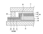
- FIG. 1 is a plan view schematically showing a solar cell module 1 as an example of an embodiment.
- FIG. 2 is a cross-sectional view of the solar cell module 1, showing a cross section of a portion where cells 2 are formed.
- illustration of the second substrate 11 is omitted, and the outline of the second substrate 11 is illustrated with a dashed line.
- the solar cell module 1 includes a cell 2 including a photoelectric conversion layer 20, a first electrode layer 30, and a second electrode layer 40, a first substrate 10, and a first substrate 10.
- a second substrate 11 that is placed opposite to each other and covers the cell 2 is provided.
- the solar cell module 1 further includes an extraction electrode layer 50 for extracting electrical energy from the cell 2, and a glass frit section 60 for bonding the two substrates together.
- the glass frit section 60 is provided between the second substrate 11 and the extraction electrode layer 50 and functions as a sealing material that seals the cell 2.
- a light-transmitting substrate is used as the first substrate 10.
- the first substrate 10, the second substrate 11, and the cell 2 are formed into a rectangular shape in plan view, and the second substrate 11, which is one size smaller than the first substrate 10, covers the entire cell 2 formed on the first substrate 10. is covered.
- the first substrate 10 and the second substrate 11 a conductive substrate with an insulating layer formed on the surface may be used, but an insulating substrate is preferably used.
- the first substrate 10 is preferably made of a material that is transparent to sunlight having a wavelength of 400 nm or more and 1000 nm or less, and has a low water vapor transmission rate. Further, a glass substrate is preferred from the viewpoint of adhesiveness and heat resistance in the glass frit fusing process.
- the thickness of the first substrate 10 is, for example, 0.3 mm or more and 3 mm or less.
- the second substrate 11 is preferably transparent to laser light, and may be a transparent substrate such as a glass substrate. Like the first substrate 10, the second substrate 11 is preferably made of a material with low water vapor permeability. The thickness of the second substrate 11 may be less than or equal to the thickness of the first substrate 10. Note that a gas barrier layer such as an alumina layer may be formed on the surfaces of the first substrate 10 and the second substrate 11. In this embodiment, flat and transparent glass substrates are used as the first substrate 10 and the second substrate 11.
- the solar cell module 1 includes a first electrode layer 30 provided on a first substrate 10, a photoelectric conversion layer 20 provided on the first electrode layer 30, and a second electrode provided on the photoelectric conversion layer 20. layer 40.
- the cell 2 is configured by the photoelectric conversion layer 20, the first electrode layer 30, and the second electrode layer 40.
- an extraction electrode layer 50 is provided on the first substrate 10, in a region that does not overlap with the photoelectric conversion layer 20 when the substrate is viewed from above.
- the extraction electrode layer 50 has a multilayer structure in which a metal layer 52 and a transparent conductive layer are laminated.
- the transparent conductive layer is provided closer to the second substrate 11 than the metal layer 52, and is in contact with the glass frit portion 60 (see FIG. 3, which will be described later).
- the glass frit part 60 covers the photoelectric conversion layer 20 (cell 2) when viewed from the Z direction, which is the lamination direction of the first electrode layer 30, the photoelectric conversion layer 20, and the second electrode layer 40. It is arranged in a ring around it.
- the extraction electrode layer 50 extends from two opposing sides of the cell 2 in a direction away from each other, and is formed beyond the range covered by the second substrate 11 to near the end of the first substrate 10 .
- the glass frit section 60 includes a first region provided between the second substrate 11 and the extraction electrode layer 50 and a second region provided between the first substrate 10 and the second substrate 11. Like the first substrate 10 and the second substrate 11, the glass frit section 60 has a low water vapor permeability and exhibits excellent sealing performance.
- a sealed internal space 4 is formed by a first substrate 10, a second substrate 11, and a glass frit part 60.
- Cell 2 is arranged in this interior space 4.
- the distance between the first substrate 10 and the second substrate 11 is, for example, 1 ⁇ m or more and 30 ⁇ m or less, and a gap exists between the cell 2 and the second substrate 11.
- the interior space 4 of the solar cell module 1 may be filled with an inert gas such as nitrogen gas. Alternatively, it may be filled with a resin such as ethylene/vinyl acetate copolymer (EVA) resin, silicone resin, or polyolefin.
- EVA ethylene/vinyl acetate copolymer
- FIG. 2 shows an example of a suitable layer structure of a solar cell
- the layer structure of the cell is not limited to this.
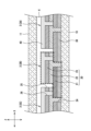
- the cell 2 is composed of a plurality of unit cells 3 connected in series.
- a plurality of unit cells 3 are arranged in the X direction, which is the first direction along the surface of the first substrate 10, and are continuous in the Y direction (see FIG. 1) orthogonal to the X direction.
- Each unit cell 3 includes a pair of electrodes (a first electrode layer 30 and a second electrode layer 40) and a photoelectric conversion layer 20 disposed between the pair of electrodes.
- the cell 2 is, for example, a perovskite solar cell.
- the first substrate 10 has optical transparency, and the photoelectric conversion layer 20 absorbs light entering the module from the first substrate 10 side to generate electricity.
- the first electrode layer 30 has light transparency and does not block light from entering the photoelectric conversion layer 20.
- the light transmittance of the first electrode layer 30 is, for example, 85% or more in the wavelength range of 450 nm or more and 900 nm or less. Further, the sheet resistance of the first electrode layer 30 is preferably 40 ⁇ / ⁇ or less, and may be 10 ⁇ / ⁇ or less.
- the first electrode layer 30 preferably has a single-layer structure made of a transparent conductive layer. As will be described in detail later, the transparent conductive layer is made of a transparent conductive oxide such as indium tin oxide (ITO).
- ITO indium tin oxide
- the second electrode layer 40 does not need to have optical transparency and includes a metal layer 42 and a transparent conductive layer.
- the second electrode layer 40 includes a first transparent conductive layer 41 and a second transparent conductive layer 43 as transparent conductive layers, and in order from the first substrate 10 side, the transparent conductive layer 41, the metal layer 42, and the transparent conductive layer It has a multilayer structure in which 43 layers are laminated.
- the metal layer is made of metals such as aluminum, nickel, copper, and silver, or alloys thereof.
- the photoelectric conversion layer 20 includes an electron transport layer 21 , a light absorption layer 22 disposed on the electron transport layer 21 , and a hole transport layer 23 disposed on the light absorption layer 22 .
- the photoelectric conversion layer 20 has a multilayer structure in which an electron transport layer 21, a light absorption layer 22, and a hole transport layer 23 are laminated in order from the first substrate 10 side, except for a portion where a groove is formed, which will be described later.
- the light absorption layer 22 includes, for example, a perovskite compound represented by the composition formula ABX 3 (wherein A is a monovalent cation, B is a divalent cation, and X is a halogen anion).
- Examples of the electron transport material constituting the electron transport layer 21 include anatase titanium oxide, tin oxide, and the like.
- Hole transport layer 23 includes a hole transport material having redox sites.
- the hole transport material constituting the hole transport layer 23 is, for example, 2,2',7,7'-tetrakis(N,N'-di-p-methoxyphenylamino)-9,9'-spirobifluorene. (Spiro-OMeTAD), etc. are exemplified.
- a in the perovskite compound (ABX 3 ) is a monovalent cation represented by R 1 R 2 R 3 --NH.
- R 1 and R 2 are H and R 3 is CH 3 , A becomes methylammonium (CH 3 NH 3 ).
- the functional groups R 1 , R 2 , and R 3 contain, for example, at least one element selected from carbon, hydrogen, nitrogen, and oxygen. When the functional groups R 1 , R 2 and R 3 contain carbon atoms, the total number of carbon atoms in the functional groups R 1 , R 2 and R 3 is preferably 4 or less.
- the functional groups R 1 , R 2 and R 3 may contain Group 1 elements such as Rb and Cs.
- B in ABX 3 is a divalent cation as described above.
- B is, for example, a transition metal or a divalent cation of a Group 13 element, a Group 14 element, or a Group 15 element.
- Specific examples of B include Pb 2+ , Ge 2+ , and Sn 2+ .
- B may contain at least one selected from Pb 2+ and Sn 2+ , and a portion of Pb 2+ and Sn 2+ may be substituted with other elements. Examples of the substitution elements include Bi, Sb, In, Ge, and Ni.
- X in ABX 3 is at least one selected from Cl, Br, and I.
- perovskite compounds include CH 3 NH 3 PbI 3 , CH 3 CH 2 NH 3 PbI 3 , NH 2 CHNH 2 PbI 3 , CH 3 NH 3 PbBr 3 , CH 3 NH 3 PbCl 3 , CsPbI 3 , CsPbBr 3 , and the like.
- the first electrode layer 30 of the unit cell 3A is electrically connected to the second electrode layer 40 of the unit cell 3B adjacent in the X direction. Further, the first electrode layer 30 of the unit cell 3B is electrically connected to the second electrode layer 40 of the unit cell 3C. In this way, the plurality of unit cells 3 are connected in series along the X direction. Further, the cell 2 has a plurality of grooves 24, 25, and 26. The grooves 24, 25, and 26 are formed, for example, to extend in the Y direction and to be substantially parallel to each other. Each groove can be formed by a conventionally known scribing method or the like.
- the groove 24 is a groove that divides the electron transport layer 21 and the first electrode layer 30 of each unit cell 3.
- the width of the groove 24 is, for example, 20 ⁇ m or more and 150 ⁇ m or less.
- the groove 25 divides the light absorption layer 22, hole transport layer 23, and second electrode layer 40 of each unit cell 3. Note that the groove 25 only needs to divide the second electrode layer 40 of each unit cell 3, and the light absorption layer 22 and the hole transport layer 23 do not need to be divided by the groove 25.
- the width of the groove 25 is, for example, 30 ⁇ m or more and 150 ⁇ m or less. In this embodiment, it is assumed that each unit cell 3 is partitioned by grooves 24 and 25.
- the groove 26 is formed to penetrate the light absorption layer 22 and the hole transport layer 23 and expose the electron transport layer 21.
- a second electrode layer 40 connected to the electron transport layer 21 of the adjacent unit cell 3 is formed in the groove 26 .
- the second electrode layer 40 is electrically connected to the first electrode layer 30 of the adjacent unit cell 3. That is, the groove 26 functions as a groove for connecting the unit cells.
- the width of the groove 26 is, for example, 150 ⁇ m or more and 300 ⁇ m or less.
- the cell 2 is manufactured, for example, by the following method.
- (1) The first electrode layer 30 and the electron transport layer 21 are formed in this order on the first substrate 10.
- (2) Part of the first electrode layer 30 and the electron transport layer 21 is laser scribed to form the groove 24 .
- Parts of the light absorption layer 22 and the hole transport layer 23 are mechanically scribed to form grooves 26 .
- Part of the light absorption layer 22, hole transport layer 23, and second electrode layer 40 is mechanically scribed to form grooves 25.
- the electron transport layer 21, the light absorption layer 22, and the hole transport layer 23 can be formed, for example, by applying a solution containing dissolved raw materials to the surface of the first substrate 10. These layers may be formed by spin coating.
- the thickness of each layer is not particularly limited, but is, for example, 10 nm or more and 100 nm or less.
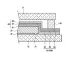
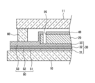
- FIGS. 3 and 4 are cross-sectional views of both ends in the X direction of the solar cell module 1 on which the extraction electrode layer 50 is formed.
- the extraction electrode layer 50 is a conductive layer including a metal layer 52 and a transparent conductive layer.
- the extraction electrode layer 50 is formed extending from the inner space 4 beyond the position where the glass frit part 60 is provided and extending over the edge of the first substrate 10 .
- the extraction electrode layer 50 is arranged on the first substrate 10 in a region that does not overlap with the photoelectric conversion layer 20 (cell 2) when the substrate is viewed from above. In other words, a conductive layer formed in a region that does not overlap with the photoelectric conversion layer 20 and drawn out from the internal space 4 is the extraction electrode layer 50 .
- the extraction electrode layer 50 having a multilayer structure including the metal layer 52 and the transparent conductive layer by using the extraction electrode layer 50 having a multilayer structure including the metal layer 52 and the transparent conductive layer, the adhesion with the glass frit part 60 is improved, and an increase in resistance of the extraction electrode layer 50 is suppressed. be done.
- the extraction electrode layer 50 includes an extraction electrode layer 50A (see FIG. 3) electrically connected to the first electrode layer 30, and an extraction electrode layer 50B (see FIG. 4) electrically connected to the second electrode layer 40. including.
- the extraction electrode layer 50A is formed at a first end in the X direction of the first substrate 10, and the extraction electrode layer 50B is formed at a second end in the X direction opposite to the first end.
- the extraction electrode layers 50A and 50B both include a metal layer 52 and a transparent conductive layer, and have the same layer structure.
- the transparent conductive layer constituting the extraction electrode layer 50 preferably includes a first transparent conductive layer 51 and a second transparent conductive layer 53.
- the extraction electrode layer 50 has a multilayer structure in which a transparent conductive layer 51, a metal layer 52, and a transparent conductive layer 53 are laminated in order from the first substrate 10 side. That is, the extraction electrode layer 50 has a three-layer structure in which a metal layer 52 is sandwiched between transparent conductive layers 51 and 53.
- a glass frit section 60 is provided between the second substrate 11 and the extraction electrode layer 50, and the glass frit section 60 is in contact with the transparent conductive layer 53.
- the second electrode layer 40 has a multilayer structure similar to the extraction electrode layer 50.
- the second electrode layer 40 includes a first transparent conductive layer 41, a metal layer 42, and a second transparent conductive layer 43, which are laminated on the photoelectric conversion layer 20 in this order from the first substrate 10 side.
- the extraction electrode layer 50B electrically connected to the second electrode layer 40 is formed continuously with the second electrode layer 40 and is separated from the first electrode layer 30 by the groove 24.
- the extraction electrode layer 50A electrically connected to the first electrode layer 30 is formed continuously with the first electrode layer 30 and separated from the second electrode layer 40 by the groove 25.
- each layer of the extraction electrode layer 50 is formed at the same time as the first electrode layer 30 and the second electrode layer 40, and after the film formation, the grooves 24 and 25 are formed to form the first electrode layer 30 or the second electrode layer 40. It is divided into 40.
- the extraction electrode layer 50 may be connected to a part of the electrode layer formed on the photoelectric conversion layer 20 in a region adjacent to the grooves 24 and 25. Since a part of the electrode layer has an extremely small area, it does not affect the characteristics of the photoelectric conversion layer 20.
- the transparent conductive layers 51 and 53 are generally made of a transparent conductive oxide in which a metal oxide such as indium oxide or zinc oxide is doped with tungsten, tin, antimony, or the like.
- a suitable transparent conductive oxide is indium tin oxide (ITO).
- the transparent conductive layers 51 and 53 are formed with substantially the same composition and the same thickness, for example, by sputtering.
- An example of the thickness of the transparent conductive layers 51 and 53 is 30 nm or more and 300 nm or less. Since the transparent conductive layers 51 and 53 are formed simultaneously with the transparent conductive layers of the first electrode layer 30 and the transparent conductive layers 41 and 43 of the second electrode layer 40, each transparent conductive layer has substantially the same composition. .
- the constituent material of the metal layer 52 is, for example, metal such as aluminum, nickel, copper, silver, or an alloy thereof. Among them, it is preferable to use silver.
- the metal layer 52 may have a single layer structure or a multilayer structure. An example of the thickness of the metal layer 52 is 80 nm or more and 500 nm or less.
- the metal layer 52 may be formed by, for example, sputtering, vapor deposition, or the like, or may be formed by a plating method. Since the metal layer 52 is deposited at the same time as the metal layer 42 of the second electrode layer 40, the metal layers 42 and 52 have substantially the same composition.
- the extraction electrode layer 50A is formed by overlapping three layers separated from the second electrode layer 40 by the groove 25 and a transparent conductive layer continuous from the first electrode layer 30.
- the extraction electrode layer 50B is formed by overlapping three layers continuous with the second electrode layer 40 and a transparent conductive layer separated from the first electrode layer 30 by the groove 24. That is, the transparent conductive layer 51 interposed between the first substrate 10 and the metal layer 52 is a transparent conductive layer derived from the first electrode layer 30 and the second electrode layer 40, and its thickness is equal to that of the second electrode layer 51. The thickness is greater than the thickness of the transparent conductive layer 53 derived only from the layer 40.
- the glass frit section 60 includes a first region provided between the second substrate 11 and the extraction electrode layer 50 and a second region provided between the first substrate 10 and the second substrate 11.
- the first region is in close contact with the second substrate 11 and the extraction electrode layer 50
- the second region is in close contact with the first substrate 10 and the second substrate 11.
- the glass frit portion 60 is formed in a thin line shape surrounding the entire circumference of the cell 2 and functions as a sealing material that seals the cell 2.
- the width of the glass frit portion 60 is not particularly limited, as an example, it is 0.1 mm or more and 1 mm or less.
- the thickness of the glass frit portion 60 is greater than the total thickness of the photoelectric conversion layer 20 and the extraction electrode layer 50.
- the glass frit section 60 is made of a glass frit material whose main component is glass having a lower melting point than the glass constituting the first substrate 10 and the second substrate 11 .
- the glass frit material is, for example, a low melting point glass powder, and most of the individual glass fine particles have a particle size of 1 ⁇ m or more and 50 ⁇ m or less.
- the composition of the low melting point glass is not particularly limited.
- the low melting point glass is, for example, mainly composed of SiO2 , Mg, Ca, Ba, Li, K, Na, Zn, Te, V, B, Pb, Al, Sn, P, Ru, Fe, Cu, Ti, It may contain at least one element selected from W, Bi, and Sb. Further, the glass frit material may contain a predetermined filler or additive.
- the glass frit section 60 is formed by forming a line of glass frit material on the first substrate 10 or the second substrate 11, overlapping the two substrates, and then applying laser irradiation along this line. It is formed by doing.
- the glass frit material is melted by laser irradiation, and the glass particles adhere to each other, as well as to the substrate and the extraction electrode layer 50, forming a dense glass frit portion 60 with a low water vapor transmission rate.
- the glass frit section 60 is a laser welding section that is melted and solidified by laser irradiation to bond two substrates together.
- the glass frit part 60 is arranged on the transparent conductive layer 53 of the extraction electrode layer 50 in the first region. That is, the glass frit part 60 is not in contact with the metal layer 52, and the transparent conductive layer 53 is interposed between the glass frit part 60 and the metal layer 52.
- the transparent conductive layer 53 has a coefficient of linear expansion closer to that of glass than the metal layer 52, and also has higher heat resistance. Therefore, by arranging the glass frit part 60 on the transparent conductive layer 53, the adhesion of the glass frit part 60 to the extraction electrode layer 50 is improved. Note that the transparent conductive layer 51 interposed between the first substrate 10 and the metal layer 52 improves the adhesion of the extraction electrode layer 50 to the first substrate 10.
- the glass frit part 60 is heated by laser irradiation, but at this time, the extraction electrode layer 50 that overlaps the glass frit part 60 also becomes high temperature, and the metal layer 52 may be damaged by the heat.
- the metal layer 52 since the metal layer 52 is sandwiched between the transparent conductive layers 51 and 53, even if the metal layer 52 is damaged, the transparent conductive layers 51 and 53 maintain a good conductive path, and the extraction electrode layer 50 Resistance increase is sufficiently suppressed. Although this effect can be obtained even when only one of the transparent conductive layers 51 and 53 is provided, by providing the transparent conductive layers 51 and 53 sandwiching the metal layer 52, the effect of suppressing the increase in resistance becomes more remarkable.
- FIG. 5 shows a cross-sectional structure of the first end of the solar cell module 1 in the X direction.
- the manufacturing process of the solar cell module 1 includes, for example, the following steps.
- (1) The first electrode layer 30, the photoelectric conversion layer 20, and the second electrode layer 40 are formed in this order on the first substrate 10, and an area that does not overlap with the photoelectric conversion layer 20 in a plan view of the first substrate 10
- On the first substrate 10 A third step (4) of placing the second substrate 11 in the glass frit material 60z and bringing the extraction electrode layer 50 prepared in the first step into contact with the glass frit material 60z prepared in the second step.
- the cell 2 including the first electrode layer 30, the photoelectric conversion layer 20, and the second electrode layer 40 is manufactured by the method described above.
- the extraction electrode layer 50 is formed simultaneously with the first electrode layer 30 and the second electrode layer 40, and in this embodiment, like the second electrode layer 40, the transparent conductive layer 51, the metal layer 52, and the transparent conductive layer Contains 53.
- the second electrode layer 40 and the extraction electrode layer 50 may have a single layer structure consisting of the metal layer 42.
- the glass frit material 60z is applied, for example, in the form of a paste containing an organic solvent onto the second substrate 11, and then the solvent is volatilized and removed by heat treatment.
- the paste of the glass frit material 60z is applied onto the second substrate 11 by a conventionally known printing method.
- the paste of the glass frit material 60z may be applied on the first substrate 10 on which the extraction electrode layer 50 is formed, but from the viewpoint of suppressing the thermal influence on the cell 2, etc., it may be applied on the second substrate 11. It is preferable that It is preferable that the glass frit material 60z is formed in a single line along the periphery of the second substrate 11 and in an annular shape.
- the glass frit part 60z is placed on the extraction electrode layer 50 by overlapping the second substrate 11 with the surface provided with the glass frit part 60z facing the first substrate 10 side.
- the glass frit material 60z is arranged in a first region disposed between the second substrate 11 and the extraction electrode layer 50 and in a second region disposed between the first substrate 10 and the second substrate 11. A region is formed. The glass frit portion 60z in the first region is then in contact with the transparent conductive layer 53 of the extraction electrode layer 50.
- the glass frit material 60z is irradiated with laser light ⁇ through the second substrate 11 from the opposite side of the metal layer.
- the laser light ⁇ has a wavelength of, for example, 800 nm or more and 1500 nm or less.
- the laser beam ⁇ is irradiated from the second substrate 11 side along the line of the glass frit material 60z.
- the glass frit material 60z melts, and the glass particles constituting the frit material come into close contact with each other, and the glass particles also come into close contact with the first substrate 10, the second substrate 11, and the extraction electrode layer 50.
- a YAG laser is used as the laser device.
- the glass frit material 60z is melted by irradiation with the laser beam ⁇ , and a glass frit portion 60 that functions as a sealing material is formed.
- the metal layer 52 of the extraction electrode layer 50 is heated and damaged, but since the metal layer 52 is sandwiched between the transparent conductive layers 51 and 53, for example, the metal layer 52 may be broken. Also, a good conductive path is maintained by the transparent conductive layers 51 and 53. As a result, an increase in resistance of the extraction electrode layer 50 is sufficiently suppressed.
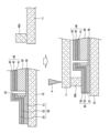
- FIG. 6 is a sectional view showing a modification of the above embodiment.
- the embodiment illustrated in FIG. 6 has the above-described features in that the extraction electrode layer 50 has a three-layer structure including a metal layer 52 and transparent conductive layers 51 and 53, and the glass frit part 60 is in contact with the transparent conductive layer 53. This is common to the embodiment.
- the second electrode layer 40 has a single layer structure made of a transparent conductive layer
- the first electrode layer 30 has a three layer structure including a metal layer 32 and transparent conductive layers 31 and 33, which is different from the above embodiment. different.
- the extraction electrode layer 50 is formed continuously with the first electrode layer 30.
- the transparent conductive layer 53 interposed between the metal layer 52 and the glass frit part 60 is a transparent conductive layer derived from the first electrode layer 30 and the second electrode layer 40, and its thickness is is larger than the thickness of the transparent conductive layer 51 derived only from the first electrode layer 30.
- the configuration is such that light can enter from the second substrate 11 side, and for example, a hole transport layer 23 is formed between the first electrode layer 30 and the light absorption layer 22, and the hole transport layer 23 is formed between the first electrode layer 30 and the light absorption layer 22.
- An electron transport layer 21 is formed between the second electrode layers 40 .
- the glass frit part 60 is annularly provided over the entire circumference of the cell 2 including the area where the extraction electrode layer 50 is formed, so that excellent sealing is achieved. Performance can be obtained.
- a durability test was conducted under conditions of a temperature of 85° C. and a humidity of 85% using a calcium film with the above three-layered extraction electrode layer 50 connected to both ends. Ta.
- the structure tested was the same as the structure of solar cell module 1 except that a calcium film was used instead of cell 2. If the calcium film does not have excellent sealing performance and absorbs water, the resistance of the calcium film increases significantly, but no increase in resistance was observed in this durability test. That is, it was demonstrated that the solar cell module 1 has excellent sealing performance.
- the extraction electrode layer 52 of the extraction electrode layer 50 is protected by the transparent conductive layers 51 and 53 sandwiching the metal layer 52. 50 resistance increase is highly suppressed.
Landscapes
- Physics & Mathematics (AREA)
- Electromagnetism (AREA)
- Photovoltaic Devices (AREA)
Abstract
Description
(1)第1基板10上に、第1電極層30および電子輸送層21をこの順で形成する。
(2)第1電極層30および電子輸送層21の一部をレーザースクライブ処理して溝24を形成する。
(3)電子輸送層21上に、光吸収層22および正孔輸送層23をこの順で形成する。
(4)光吸収層22および正孔輸送層23の一部をメカニカルスクライブ処理して溝26を形成する。
(5)正孔輸送層23上に、第2電極層40を形成する。
(6)光吸収層22、正孔輸送層23、および第2電極層40の一部をメカニカルスクライブ処理して溝25を形成する。
(1)第1基板10上に、第1電極層30、光電変換層20、および第2電極層40をこの順に形成すると共に、第1基板10の平面視において光電変換層20と重ならない領域に金属層と透明導電層とが積層された取り出し電極層50を形成する第1の工程
(2)第2基板11上にガラスフリット材60zを設ける第2の工程
(3)第1基板10上に第2基板11を配置し、第1の工程で準備された取り出し電極層50と、第2の工程で準備されたガラスフリット材60zとを接触させる第3の工程
(4)ガラスフリット材60zによって、取り出し電極層50と第2基板11とを接着し固定する第4の工程
Claims (9)
- 第1基板と、
前記第1基板上に設けられた第1電極層と、
前記第1電極層上に設けられた光電変換層と、
前記光電変換層上に設けられた第2電極層と、
前記第1基板上において、当該基板を平面視したときに前記光電変換層と重ならない領域に設けられ、金属層と透明導電層とが積層された取り出し電極層と、
前記第1電極層、前記光電変換層、前記第2電極層、および前記取り出し電極層を覆うように設けられた第2基板と、
前記第2基板と前記取り出し電極層との間に設けられたガラスフリット部と、
を備えた、太陽電池モジュール。 - 前記取り出し電極層の前記透明導電層は、前記金属層よりも前記第2基板の近くに設けられ、
前記ガラスフリット部は、前記透明導電層に接触する、請求項1に記載の太陽電池モジュール。 - 前記透明導電層は、第1および第2の透明導電層を含み、
前記取り出し電極層は、前記第1基板側から順に、前記第1の透明導電層、前記金属層、および前記第2の透明導電層が積層された複層構造を有し、
前記ガラスフリット部は、前記第2の透明導電層に接触する、請求項2に記載の太陽電池モジュール。 - 前記第2電極層は、前記金属層および前記透明導電層を含み、
前記取り出し電極層は、前記第2電極層と連続的に形成されている、請求項1-3のいずれか1項に記載の太陽電池モジュール。 - 前記第1電極層は、前記金属層および前記透明導電層を含み、
前記取り出し電極層は、前記第1電極層と連続的に形成されている、請求項1-3のいずれか1項に記載の太陽電池モジュール。 - 前記ガラスフリット部は、前記第1電極層、前記光電変換層、および前記第2電極層の積層方向から見たときに、前記光電変換層を囲んで環状に設けられ、前記第2基板と前記取り出し電極層との間に設けられた第1領域と、前記第1基板と前記第2基板との間に設けられた第2領域と、を含む、請求項1-3のいずれか1項に記載の太陽電池モジュール。
- 前記光電変換層は、
電子輸送層と、
前記電子輸送層上に配置され、組成式ABX3(式中、Aは1価のカチオン、Bは2価のカチオン、Xはハロゲンアニオン)で示されるペロブスカイト化合物を含む光吸収層と、
前記光吸収層上に配置された正孔輸送層と、
を含む、請求項1-3のいずれか1項に記載の太陽電池モジュール。 - 第1基板上に、第1電極層、光電変換層、および第2電極層をこの順に形成すると共に、前記第1基板の平面視において前記光電変換層と重ならない領域に金属層と透明導電層とが積層された取り出し電極層を形成する第1の工程と、
第2基板上にガラスフリット材を設ける第2の工程と、
前記第1基板上に前記第2基板を配置し、前記第1の工程で準備された前記取り出し電極層と、前記第2の工程で準備されたガラスフリット材とを接触させる第3の工程と、
前記ガラスフリット材によって、前記取り出し電極層と前記第2基板とを接着し固定する第4の工程と、
を含む、太陽電池モジュールの製造方法。 - 前記第4の工程では、前記ガラスフリット材に対し、前記第1基板または前記第2基板を介してレーザー照射する、請求項8に記載の太陽電池モジュールの製造方法。
Priority Applications (3)
| Application Number | Priority Date | Filing Date | Title |
|---|---|---|---|
| EP23807607.9A EP4529392A4 (en) | 2022-05-20 | 2023-05-15 | SOLAR CELL MODULE AND METHOD FOR MANUFACTURING THE SOLAR CELL MODULE |
| CN202380040276.XA CN119256640A (zh) | 2022-05-20 | 2023-05-15 | 太阳能电池模块及太阳能电池模块的制造方法 |
| US18/948,845 US20250072199A1 (en) | 2022-05-20 | 2024-11-15 | Solar cell module and method for manufacturing solar cell module |
Applications Claiming Priority (2)
| Application Number | Priority Date | Filing Date | Title |
|---|---|---|---|
| JP2022-082874 | 2022-05-20 | ||
| JP2022082874A JP2023170819A (ja) | 2022-05-20 | 2022-05-20 | 太陽電池モジュールおよび太陽電池モジュールの製造方法 |
Related Child Applications (1)
| Application Number | Title | Priority Date | Filing Date |
|---|---|---|---|
| US18/948,845 Continuation US20250072199A1 (en) | 2022-05-20 | 2024-11-15 | Solar cell module and method for manufacturing solar cell module |
Publications (1)
| Publication Number | Publication Date |
|---|---|
| WO2023224005A1 true WO2023224005A1 (ja) | 2023-11-23 |
Family
ID=88835619
Family Applications (1)
| Application Number | Title | Priority Date | Filing Date |
|---|---|---|---|
| PCT/JP2023/018128 Ceased WO2023224005A1 (ja) | 2022-05-20 | 2023-05-15 | 太陽電池モジュールおよび太陽電池モジュールの製造方法 |
Country Status (5)
| Country | Link |
|---|---|
| US (1) | US20250072199A1 (ja) |
| EP (1) | EP4529392A4 (ja) |
| JP (1) | JP2023170819A (ja) |
| CN (1) | CN119256640A (ja) |
| WO (1) | WO2023224005A1 (ja) |
Cited By (2)
| Publication number | Priority date | Publication date | Assignee | Title |
|---|---|---|---|---|
| WO2025186653A1 (en) * | 2024-03-04 | 2025-09-12 | Ricoh Company, Ltd. | Photoelectric conversion element, solar cell module, electronic device, and power supply module |
| WO2025197513A1 (ja) * | 2024-03-22 | 2025-09-25 | 株式会社カネカ | 太陽電池モジュール |
Citations (7)
| Publication number | Priority date | Publication date | Assignee | Title |
|---|---|---|---|---|
| JP2003123857A (ja) * | 2001-10-19 | 2003-04-25 | Bridgestone Corp | 有機色素増感型金属酸化物半導体電極及びこの半導体電極を有する太陽電池 |
| WO2010098311A1 (ja) * | 2009-02-24 | 2010-09-02 | 株式会社フジクラ | 光電変換素子 |
| JP2011054477A (ja) | 2009-09-03 | 2011-03-17 | Sharp Corp | 有機エレクトロルミネッセンス表示装置、および有機エレクトロルミネッセンス表示装置の製造方法 |
| US20150056736A1 (en) * | 2013-08-21 | 2015-02-26 | Markus Eberhard Beck | Methods of hermetically sealing photovoltaic modules |
| JP2016063189A (ja) * | 2014-09-22 | 2016-04-25 | 株式会社東芝 | 光電変換装置 |
| JP2016531443A (ja) * | 2013-08-23 | 2016-10-06 | フラウンホッファー−ゲゼルシャフト・ツァー・フォデラング・デル・アンゲワンテン・フォーシュング・エー.ファウ. | 溶液から析出可能な長期安定型光起電力素子及びその製造方法 |
| JP2019021913A (ja) | 2017-07-11 | 2019-02-07 | パナソニック株式会社 | 太陽電池モジュール |
Family Cites Families (3)
| Publication number | Priority date | Publication date | Assignee | Title |
|---|---|---|---|---|
| DE102009046755A1 (de) * | 2009-11-17 | 2011-05-26 | Fraunhofer-Gesellschaft zur Förderung der angewandten Forschung e.V. | Organisches photoelektrisches Bauelement |
| WO2014181765A1 (ja) * | 2013-05-09 | 2014-11-13 | ローム株式会社 | 有機薄膜太陽電池およびその製造方法 |
| DE102013111739B4 (de) * | 2013-10-24 | 2024-08-22 | Pictiva Displays International Limited | Optoelektronisches Bauelement und Verfahren zum Herstellen eines optoelektronischen Bauelements |
-
2022
- 2022-05-20 JP JP2022082874A patent/JP2023170819A/ja active Pending
-
2023
- 2023-05-15 EP EP23807607.9A patent/EP4529392A4/en active Pending
- 2023-05-15 WO PCT/JP2023/018128 patent/WO2023224005A1/ja not_active Ceased
- 2023-05-15 CN CN202380040276.XA patent/CN119256640A/zh active Pending
-
2024
- 2024-11-15 US US18/948,845 patent/US20250072199A1/en active Pending
Patent Citations (7)
| Publication number | Priority date | Publication date | Assignee | Title |
|---|---|---|---|---|
| JP2003123857A (ja) * | 2001-10-19 | 2003-04-25 | Bridgestone Corp | 有機色素増感型金属酸化物半導体電極及びこの半導体電極を有する太陽電池 |
| WO2010098311A1 (ja) * | 2009-02-24 | 2010-09-02 | 株式会社フジクラ | 光電変換素子 |
| JP2011054477A (ja) | 2009-09-03 | 2011-03-17 | Sharp Corp | 有機エレクトロルミネッセンス表示装置、および有機エレクトロルミネッセンス表示装置の製造方法 |
| US20150056736A1 (en) * | 2013-08-21 | 2015-02-26 | Markus Eberhard Beck | Methods of hermetically sealing photovoltaic modules |
| JP2016531443A (ja) * | 2013-08-23 | 2016-10-06 | フラウンホッファー−ゲゼルシャフト・ツァー・フォデラング・デル・アンゲワンテン・フォーシュング・エー.ファウ. | 溶液から析出可能な長期安定型光起電力素子及びその製造方法 |
| JP2016063189A (ja) * | 2014-09-22 | 2016-04-25 | 株式会社東芝 | 光電変換装置 |
| JP2019021913A (ja) | 2017-07-11 | 2019-02-07 | パナソニック株式会社 | 太陽電池モジュール |
Non-Patent Citations (1)
| Title |
|---|
| See also references of EP4529392A4 |
Cited By (2)
| Publication number | Priority date | Publication date | Assignee | Title |
|---|---|---|---|---|
| WO2025186653A1 (en) * | 2024-03-04 | 2025-09-12 | Ricoh Company, Ltd. | Photoelectric conversion element, solar cell module, electronic device, and power supply module |
| WO2025197513A1 (ja) * | 2024-03-22 | 2025-09-25 | 株式会社カネカ | 太陽電池モジュール |
Also Published As
| Publication number | Publication date |
|---|---|
| EP4529392A4 (en) | 2025-08-13 |
| CN119256640A (zh) | 2025-01-03 |
| EP4529392A1 (en) | 2025-03-26 |
| JP2023170819A (ja) | 2023-12-01 |
| US20250072199A1 (en) | 2025-02-27 |
Similar Documents
| Publication | Publication Date | Title |
|---|---|---|
| US20250072199A1 (en) | Solar cell module and method for manufacturing solar cell module | |
| JP5629010B2 (ja) | 改良された光起電力セルアセンブリ及び方法 | |
| JP6082046B2 (ja) | 改良された光起電力セルアセンブリ | |
| US10056504B2 (en) | Photovoltaic module | |
| US10636923B2 (en) | Photovoltaic module encapsulation | |
| JP2020092267A (ja) | 太陽電池とその製造方法及び太陽電池パネル | |
| JP5286325B2 (ja) | 染料感応型太陽電池の製造方法 | |
| US20160181454A1 (en) | Solar cell module and method for manufacturing the same | |
| WO2021220925A1 (ja) | 太陽電池 | |
| JP2026004326A (ja) | 光電変換モジュール | |
| US9991402B2 (en) | Solar apparatus and method of fabricating the same | |
| JP2017152510A (ja) | 太陽電池モジュールの製造方法及び太陽電池モジュール | |
| US9391219B2 (en) | Photovoltaic apparatus | |
| WO2024247789A1 (ja) | 光電変換素子の製造方法および光電変換素子 | |
| CN113841258B (zh) | 太阳能电池模块 | |
| US20250228058A1 (en) | Solar cell module and method for manufacturing solar cell module | |
| JP2004200512A (ja) | 光電変換装置 | |
| US20250248135A1 (en) | 3t tandem solar cell, tandem solar cell module, and method for producing same | |
| WO2023189907A1 (ja) | 太陽電池モジュール製造方法 | |
| US20130125960A1 (en) | Photoelectric conversion device | |
| JP2025180024A (ja) | 太陽電池モジュール及び太陽電池モジュールの製造方法 | |
| US20140054735A1 (en) | Photoelectric conversion module | |
| JP2026003986A (ja) | 太陽電池モジュール | |
| WO2024203678A1 (ja) | 太陽電池モジュール | |
| JP2026022899A (ja) | 太陽電池モジュール及びその製造方法 |
Legal Events
| Date | Code | Title | Description |
|---|---|---|---|
| 121 | Ep: the epo has been informed by wipo that ep was designated in this application |
Ref document number: 23807607 Country of ref document: EP Kind code of ref document: A1 |
|
| WWE | Wipo information: entry into national phase |
Ref document number: 202380040276.X Country of ref document: CN |
|
| WWE | Wipo information: entry into national phase |
Ref document number: 2023807607 Country of ref document: EP |
|
| NENP | Non-entry into the national phase |
Ref country code: DE |
|
| ENP | Entry into the national phase |
Ref document number: 2023807607 Country of ref document: EP Effective date: 20241220 |
|
| WWP | Wipo information: published in national office |
Ref document number: 202380040276.X Country of ref document: CN |