WO2023238608A1 - 表面加工方法 - Google Patents
表面加工方法 Download PDFInfo
- Publication number
- WO2023238608A1 WO2023238608A1 PCT/JP2023/018139 JP2023018139W WO2023238608A1 WO 2023238608 A1 WO2023238608 A1 WO 2023238608A1 JP 2023018139 W JP2023018139 W JP 2023018139W WO 2023238608 A1 WO2023238608 A1 WO 2023238608A1
- Authority
- WO
- WIPO (PCT)
- Prior art keywords
- workpiece
- processed
- surface processing
- processing method
- alkaline electrolyte
- Prior art date
- Legal status (The legal status is an assumption and is not a legal conclusion. Google has not performed a legal analysis and makes no representation as to the accuracy of the status listed.)
- Ceased
Links
Images


Classifications
-
- C—CHEMISTRY; METALLURGY
- C25—ELECTROLYTIC OR ELECTROPHORETIC PROCESSES; APPARATUS THEREFOR
- C25D—PROCESSES FOR THE ELECTROLYTIC OR ELECTROPHORETIC PRODUCTION OF COATINGS; ELECTROFORMING; APPARATUS THEREFOR
- C25D11/00—Electrolytic coating by surface reaction, i.e. forming conversion layers
- C25D11/02—Anodisation
- C25D11/32—Anodisation of semiconducting materials
-
- B—PERFORMING OPERATIONS; TRANSPORTING
- B23—MACHINE TOOLS; METAL-WORKING NOT OTHERWISE PROVIDED FOR
- B23H—WORKING OF METAL BY THE ACTION OF A HIGH CONCENTRATION OF ELECTRIC CURRENT ON A WORKPIECE USING AN ELECTRODE WHICH TAKES THE PLACE OF A TOOL; SUCH WORKING COMBINED WITH OTHER FORMS OF WORKING OF METAL
- B23H5/00—Combined machining
-
- C—CHEMISTRY; METALLURGY
- C25—ELECTROLYTIC OR ELECTROPHORETIC PROCESSES; APPARATUS THEREFOR
- C25F—PROCESSES FOR THE ELECTROLYTIC REMOVAL OF MATERIALS FROM OBJECTS; APPARATUS THEREFOR
- C25F3/00—Electrolytic etching or polishing
- C25F3/16—Polishing
-
- H—ELECTRICITY
- H10—SEMICONDUCTOR DEVICES; ELECTRIC SOLID-STATE DEVICES NOT OTHERWISE PROVIDED FOR
- H10P—GENERIC PROCESSES OR APPARATUS FOR THE MANUFACTURE OR TREATMENT OF DEVICES COVERED BY CLASS H10
- H10P52/00—Grinding, lapping or polishing of wafers, substrates or parts of devices
-
- H—ELECTRICITY
- H10—SEMICONDUCTOR DEVICES; ELECTRIC SOLID-STATE DEVICES NOT OTHERWISE PROVIDED FOR
- H10P—GENERIC PROCESSES OR APPARATUS FOR THE MANUFACTURE OR TREATMENT OF DEVICES COVERED BY CLASS H10
- H10P52/00—Grinding, lapping or polishing of wafers, substrates or parts of devices
- H10P52/40—Chemomechanical polishing [CMP]
- H10P52/402—Chemomechanical polishing [CMP] of semiconductor materials
-
- H—ELECTRICITY
- H10—SEMICONDUCTOR DEVICES; ELECTRIC SOLID-STATE DEVICES NOT OTHERWISE PROVIDED FOR
- H10P—GENERIC PROCESSES OR APPARATUS FOR THE MANUFACTURE OR TREATMENT OF DEVICES COVERED BY CLASS H10
- H10P90/00—Preparation of wafers not covered by a single main group of this subclass, e.g. wafer reinforcement
- H10P90/12—Preparing bulk and homogeneous wafers
- H10P90/129—Preparing bulk and homogeneous wafers by polishing
Definitions
- the present disclosure relates to a surface processing method for flattening a processed surface, which is the surface of a processed object.
- Patent Document 1 provides a polishing method using anodic oxidation that can highly efficiently create a difficult-to-process material such as single-crystal SiC into a desired shape with a scratch-free and damage-free high-quality surface.
- the polishing method disclosed in Patent Document 1 includes an anodizing process and a polishing process.
- the anodic oxidation process is a process in which an oxide film is formed on the surface of the workpiece by applying a voltage to the workpiece as an anode in the presence of an electrolytic solution and flowing a current at a predetermined current density.
- the polishing process is a process in which the oxide film is selectively removed by polishing using a polishing material having a Mohs hardness intermediate between that of the workpiece and the oxide film.
- the polishing method disclosed in Patent Document 1 flattens the surface of the workpiece by simultaneously performing an anodizing process and a polishing process. Note that the polishing method disclosed in Patent Document 1 is included in a technique called ECMP.
- ECMP is an abbreviation for Electro-Chemical Mechanical Polishing.
- the present disclosure provides a technology that makes it possible to achieve both high processing speed and good surface roughness in a surface processing method (e.g., a grinding method, a rough polishing method, or a polishing method) that uses anodic oxidation, for example. It provides:
- a surface processing method is a method for flattening a surface to be processed, which is a surface of a workpiece, and includes the following procedures, treatments, or steps: With the grinding wheel layer and the surface to be processed facing each other with an alkaline electrolyte sandwiched therebetween, current is passed through the object to be processed as an anode, thereby generating oxides on the surface to be processed by anodic oxidation. , The oxide generated on the processed surface by anodic oxidation is removed by the grindstone layer.
- each element may be given a reference numeral in parentheses.
- the reference numerals indicate only one example of the correspondence between the same elements and specific configurations described in the embodiments described later. Therefore, the present disclosure is not limited in any way by the description of the reference numerals.
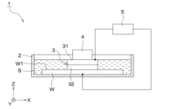
- FIG. 1 is a schematic configuration diagram of a surface processing apparatus for implementing a surface processing method according to an embodiment of the present disclosure.
- FIG. 6 is a plan view showing the surface roughness measurement positions of the processed surfaces after polishing in Examples and Comparative Examples. It is a graph showing the surface roughness measurement results of the processed surfaces after polishing in Examples and Comparative Examples. It is a graph showing the measurement results of the hardness of the oxide film generated on the processed surface in Examples and Comparative Examples.
- 2 is a graph showing ECMP polishing rates of SiC wafers as workpieces according to Examples and Comparative Examples. 2 is a graph showing the ECMP polishing rate of Si0 2 optical glass as a workpiece according to Examples and Comparative Examples.
- the surface processing apparatus 1 is configured to be capable of flattening a surface W1 to be processed, which is one principal surface of the workpiece W.
- "Flattening” is, for example, grinding or polishing, and specifically, for example, rough grinding, finish grinding, rough polishing, or final polishing.
- the "principal surface” is a surface perpendicular to the thickness direction of a layered object or a plate-like object, and is also referred to as a "plate surface.”
- the surface processing apparatus 1 is configured to be able to perform flattening processing using anodic oxidation on the processing surface W1 of the workpiece W.
- the surface processing device 1 has a configuration as an ECMP device or an ECMG device.
- ECMG is an abbreviation for Electro-Chemical Mechanical Grinding.
- the workpiece W is, for example, a silicon-based material, typically a semiconductor material such as a silicon carbide semiconductor.
- the surface processing device 1 includes a container 2, a surface processing pad 3, a drive device 4, and a power supply device 5.
- FIG. 1 and the following explanation using it are simplified for the purpose of simply explaining the surface processing method according to the present embodiment, and are not applicable to actual manufacturing and sales. It does not necessarily match the specific device configuration.
- a right-handed XYZ coordinate system is set as shown.
- the Z-axis positive direction indicates vertically upward, that is, the direction opposite to the direction of weight action.
- the X-axis direction and the Y-axis direction which are orthogonal to each other, both indicate the horizontal direction.
- the Z-axis positive direction side corresponding to the vertically upward direction may be simply referred to as "upward,” and the opposite may be simply referred to as "downward.”
- the container 2 is formed into a bathtub shape that opens upward.
- the container 2 is configured to hold the workpiece W at the bottom and accommodate the workpiece W while being immersed in an electrolytic solution S that does not contain an etchant component.
- the etchant component is a component constituting a solution having the ability to dissolve the oxide film (that is, the oxide produced in the form of a film) produced on the surface W1 to be processed by anodic oxidation, and includes, for example, hydrofluoric acid, etc. It is.
- the electrolytic solution S used in this embodiment, which does not contain an etchant component is an alkaline electrolytic solution with a pH of 9 to 13.
- the basic compound for adjusting the pH of the electrolytic solution S to 9 to 13 for example, potassium hydroxide, sodium hydroxide, lithium hydroxide, calcium hydroxide, etc. can be used.
- Surface processing pad 3 and drive device 4 are arranged above container 2 .
- the container 2, the surface processing pad 3, and the drive device 4 are provided so as to be relatively movable in the vertical direction by a lifting mechanism (not shown). Further, the container 2, the surface processing pad 3, and the drive device 4 are provided so as to be relatively movable in the in-plane direction (that is, horizontal direction) along the surface to be processed W1 by a slide mechanism (not shown).
- the surface processing pad 3 has an electrode 31 and a grindstone layer 32.
- the electrode 31 is a plate-shaped member made of a good conductor such as metal, and is formed of, for example, a copper plate.
- the grindstone layer 32 is joined to the electrode 31. That is, the surface processing pad 3 has a structure in which the electrode 31 and the grindstone layer 32 are joined in the thickness direction of the surface processing pad 3.
- the grindstone layer 32 is formed of an abrasive material or a grindstone that is an abrasive material (for example, a ceria grindstone, etc.).
- the surface processing pad 3 is provided such that the grindstone layer 32 is disposed opposite to the surface W1 to be processed of the workpiece W with the electrolyte solution S interposed therebetween.
- the surface processing pad 3 is rotated by the drive device 4 with the grinding wheel layer 32 disposed opposite to the surface to be processed W1 with the electrolyte S sandwiched therebetween, so that the surface processing pad 3 has abrasive particles formed on the surface to be processed by anodization by anodic oxidation.
- the oxide film can be selectively removed by polishing or polishing.
- the drive device 4 is configured to rotate the surface processing pad 3 around a rotation axis along the vertical direction.
- the power supply device 5 applies a voltage with the workpiece W as an anode and the electrode 31 of the surface processing pad 3 as a cathode in the presence of an electrolytic solution S, so that the workpiece surface W1 to be processed by the grinding wheel layer 32 becomes an anode. It is provided to pass an anodic oxidation current, which is a current for oxidation.
- the surface processing method (i.e., grinding method or polishing method) of the workpiece W according to this embodiment is a method for flattening the workpiece surface W1, which is the surface of the workpiece W, and is shown in FIG. This is carried out using a surface processing apparatus 1.
- the surface processing method according to the present embodiment includes the following procedures, treatments, or steps: (1) With the grinding wheel layer 32 and the workpiece surface W1 facing each other with the alkaline electrolyte S in between, a current is passed through the workpiece W as an anode, and the workpiece surface W1 is anodized by anodic oxidation. generates an oxide film. (2) The oxide film generated on the processed surface W1 by anodic oxidation is removed by the grindstone layer 32.
- the oxide film formed in the form of a film on the workpiece surface W1 by anodic oxidation has lower hardness than the non-oxidized region. Therefore, by rubbing the processed surface W1 with the grindstone layer 32, the oxide film is selectively removed from the processed surface W1. Thereby, the processed surface W1 is satisfactorily flattened to a desired surface roughness. Note that the generation of the oxide film by anodic oxidation and the removal of the oxide film by the grindstone layer 32 may be performed simultaneously or with a time difference.
- the surface processing method according to the present embodiment can be well applied, for example, to surface planarization processing of semiconductor materials such as SiC wafers, which require nano-level surface roughness.
- this type of surface flattening processing currently determines the lead time in semiconductor wafer manufacturing. Therefore, in this type of surface flattening processing, improving the processing speed as much as possible (that is, without degrading processing quality) leads to improving manufacturing efficiency in semiconductor wafer manufacturing.
- the inventor has found that in conventional ECMP and ECMG, when attempting to improve the machining speed, many scratches occur on the processed surface W1, resulting in increased surface roughness. I found it.
- the inventors considered the factors and found the following points of interest.
- Mechanism 1 By controlling the potentials of the processed surface W1 and the sludge, sludge aggregation is suppressed, and sludge adhesion to the processed surface W1 is suppressed.
- Mechanism 2 By reducing the hardness of the oxide film generated by anodic oxidation and lowering the pressure during processing, generation of distortion and scratches on the processed surface W1 is suppressed.
- the inventors discovered a method of using an alkaline aqueous solution as the electrolyte S in anodization.
- an alkaline electrolyte for anodizing, the zeta potentials of the workpiece W and sludge can be made negative. This makes it possible to suppress agglomeration of sludge and abrasive grains released from the grindstone layer 32, and to suppress adhesion of sludge to the processed surface W1.
- the hardness of the oxide film generated during anodic oxidation can be reduced, thereby making it easier to remove the oxide film using the grindstone layer 32.
- the oxide film can be removed at low pressure. Furthermore, the wear rate of the grindstone layer 32 is reduced. Therefore, according to this embodiment, it is possible to achieve both high processing speed and good surface roughness.
- Example 1 Surface roughness
- the workpiece surface W1 is The finished state. Specifically, processing was performed for 30 minutes at a current density of 10 mA/cm 2 DC, and the surface roughness Ra of a total of 9 points P1 to P9 on the processed surface W1 shown in FIG. Measurement was performed using a scanning white interferometer New View 8300. The measurement results are shown in Figure 3.
- FIG. 3 shows the average value of nine points as a bar graph, and also shows the variance ⁇ , which is a statistical value corresponding to the dispersion, as a vertical line segment. As shown in FIG.
- FIG. 4 shows the results of measuring the hardness of the oxide film generated on the processed surface W1.
- the electrolytic solution S and current conditions are the same as above.
- the hardness of the oxide film was measured by a micro-Vickers hardness test in accordance with JIS Z2244 using a TI980 triboindenter manufactured by Bruker.
- the indentation depth was 200 nm.
- the variance ⁇ which is a statistical value corresponding to the dispersion of measured values at multiple points, is shown by a vertical line segment.
- the use of an alkaline electrolyte reduced the hardness of the oxide film.
- FIG. 5 shows the evaluation results of the polishing rate in ECMP using a SiC wafer as the workpiece W.
- FIG. 6 shows the evaluation results of the polishing rate in ECMP using Si0 2 optical glass as the workpiece W.
- the polishing rate of SiC wafers was approximately doubled.
- the polishing rate of Si0 2 optical glass was improved about three times. From these results, it can be understood that the polishing rate is improved by the chemical reaction between the oxide film and the alkaline electrolyte.
- FIG. 7 shows the results of evaluating the pH dependence of the polishing rate when the pH of the electrolytic solution S was changed in ECMP using a SiC wafer as the workpiece W.
- pH 12 and pH 12.5 are assumed to be a "fresh" alkaline electrolyte with no history of use.
- the polishing rate was almost constant when the pH was between 9 and 12.5, and the polishing rate was about twice that of the case where the pH was about 7, that is, salt water. . It was confirmed that this could effectively suppress the occurrence of deterioration in processing speed and processing quality due to changes in the properties of the alkaline electrolyte over time.
- FIG. 8 shows the results of evaluating the removal rate of silica particles from the workpiece surface W1 in ECMP using a SiC wafer as the workpiece W.
- FIG. 9 shows the results of evaluating the removal rate of ceria fine particles from the workpiece surface W1 in ECMP using a SiC wafer as the workpiece W.
- a circle mark indicates a particle diameter of 0.2 ⁇ m
- a triangle mark indicates a particle diameter of 0.3 ⁇ m
- an x mark indicates a particle diameter of 0.5 ⁇ m.
- the removal rate was evaluated by measuring the wafer surface before and after processing using a surface foreign matter inspection device manufactured by YGK. As shown in FIGS.
- FIG. 1 and the above explanation using the same are simplified solely for explaining the general configuration and functions of the surface processing apparatus 1 according to the present embodiment, and are It does not necessarily match the specific device configuration.
- the workpiece W is held on the side of the container 2, while the surface processing pad 3 is rotatably held above the workpiece W. was.
- the present disclosure is not limited to such aspects. That is, for example, there may be a configuration in which the workpiece W is held on the side of the chuck placed above the container 2 and rotationally driven by the drive device 4, while the surface processing pad 3 is held on the side of the container 2.
- the electrolyte S may contain an etchant component. That is, the surface processing method according to the present disclosure polishes or grinds the surface to be processed W1 by selectively removing the oxide film generated by anodic oxidation using both an etchant and the surface processing pad 3. It's okay.
- the present disclosure can be successfully applied to any workpiece W that can be subjected to surface flattening using anodic oxidation. Note that "using anodic oxidation” can also be expressed as “using anodic oxidation.” Further, when the workpiece W is a semiconductor ingot or wafer, there is no particular limitation on the diameter, and the present disclosure is suitable for sizes of 1 to 8 inches as well as the typical 6 inch size. Applicable to
- the surface processing pad 3 for example, the grit or material of the grindstone layer 32. That is, the details of the structure of the surface processing pad 3 (for example, the grindstone layer 32, the material, etc.) may be appropriately selected from available materials within a range in which the effects of the present disclosure can be satisfactorily exhibited.
- modified examples are also not limited to the above examples. That is, for example, a plurality of embodiments other than those exemplified above may be combined with each other unless technically inconsistent. Similarly, multiple variants may be combined with each other unless technically contradictory.
- the surface processing method for flattening the surface to be processed (W1) that is the surface of the workpiece (W) includes the following treatments, procedures, or steps: With the grinding wheel layer (32) and the surface to be machined facing each other with the alkaline electrolyte (S) in between, current is passed through the workpiece using the object as an anode, whereby the surface to be processed is anodized. to generate oxides, The oxide generated on the processed surface by anodic oxidation is removed by the grindstone layer.
- the alkaline electrolyte has a pH of 9 to 13.
- the workpiece is a silicon-based material.
- the workpiece is a silicon carbide semiconductor.
- the workpiece is a silicon carbide semiconductor.
- the hardness of the oxide is reduced by anodic oxidation using the alkaline electrolyte, thereby facilitating the removal of the oxide by the grindstone layer.
Landscapes
- Chemical & Material Sciences (AREA)
- Engineering & Computer Science (AREA)
- Chemical Kinetics & Catalysis (AREA)
- Electrochemistry (AREA)
- Materials Engineering (AREA)
- Metallurgy (AREA)
- Organic Chemistry (AREA)
- Mechanical Engineering (AREA)
- Mechanical Treatment Of Semiconductor (AREA)
Abstract
Description
本開示は、上記に例示した事情等に鑑みてなされたものである。すなわち、本開示は、例えば、陽極酸化を援用した表面加工方法(例えば、研削方法、粗研磨方法、あるいは研磨方法)において、高い加工速度と良好な表面粗さとを両立させることを可能とする技術を提供するものである。
アルカリ性電解液を挟んで砥石層と前記被加工面とを対向配置させた状態で、前記被加工物を陽極として電流を通流させることで、陽極酸化により前記被加工面に酸化物を生成させ、
陽極酸化により前記被加工面に生成した前記酸化物を、前記砥石層により除去する。
以下、本開示の実施形態を、図面に基づいて説明する。なお、一つの実施形態に対して適用可能な各種の変形例については、当該実施形態に関する一連の説明の途中に挿入されると、当該実施形態の理解が妨げられるおそれがある。このため、変形例については、当該実施形態に関する一連の説明の途中には挿入せず、その後にまとめて説明する。
図1を参照すると、表面加工装置1は、被加工物Wの一主面である被加工面W1を平坦化可能に構成されている。「平坦化」は、例えば、研削または研磨であり、具体的には、例えば、粗研削、仕上げ研削、粗研磨、または仕上げ研磨である。「主面」は、層状物あるいは板状物における、厚さ方向と直交する表面であって、「板面」とも称される。具体的には、本実施形態においては、表面加工装置1は、被加工物Wの被加工面W1に対して陽極酸化を援用した平坦化加工を実施可能に構成されている。すなわち、表面加工装置1は、ECMP装置あるいはECMG装置としての構成を有している。ECMGはElectro-Chemical Mechanical Grindingの略である。被加工物Wは、例えば、ケイ素系材料であって、典型的には炭化ケイ素半導体等の半導体材料である。
本実施形態に係る、被加工物Wの表面加工方法(すなわち研削方法あるいは研磨方法)は、被加工物Wの表面である被加工面W1を平坦化する方法であって、図1に示された表面加工装置1を用いて行われる。具体的には、本実施形態に係る表面加工方法は、以下の手順、処理、あるいは工程を含む:
(1)アルカリ性の電解液Sを挟んで砥石層32と被加工面W1とを対向配置させた状態で、被加工物Wを陽極として電流を通流させることで、陽極酸化により被加工面W1に酸化膜を生成させる。
(2)陽極酸化により被加工面W1に生成した酸化膜を、砥石層32により除去する。
(着眼点1)凝集したスラッジが、被加工物Wや砥石層32に付着することで加工界面に噛み込まれ、これによりスクラッチが発生する。
(着眼点2)陽極酸化により発生する酸化膜の硬度が高いため、加工時に高い圧力が必要となり、これにより、被加工面W1に歪が入ることでスクラッチが発生する。
(メカニズム1)被加工面W1およびスラッジの電位を制御することで、スラッジの凝集を抑制するとともに、スラッジの被加工面W1への付着を抑制する。
(メカニズム2)陽極酸化により発生する酸化膜の硬度を低下させ、加工時の圧力を低圧化することで、被加工面W1における歪およびスクラッチの発生を抑制する。
まず、被加工物WとしてSiCウェハを用いたECMPにおいて、電解液SとしてpH7の塩水とpH12のアルカリ電解水(具体的には水酸化カリウム水溶液)とを用いた場合の、被加工面W1の仕上がり状態を評価した。具体的には、直流10mA/cm2の電流密度で30分間の加工を行い、図2に示されている被加工面W1におけるP1~P9の合計9点の表面粗さRaを、ZYGO社製 走査型白色干渉計 New View 8300によって測定した。測定結果を図3に示す。図3は、9点の平均値を棒グラフで示すとともに、バラツキに対応する統計値である分散σを縦方向の線分で示す。図3に示されているように、アルカリ性電解液を用いることで、表面粗さの平均値とバラツキとの双方について向上することが確認された。また、外観観察したところ、比較例すなわち塩水の場合には被加工面W1上に多量のスクラッチがほぼ全面にわたって発生していたが、実施例すなわちアルカリ水の場合にはスクラッチはほとんど発生していなかった。
図4は、被加工面W1に発生した酸化膜の硬度を測定した結果を示す。電解液Sおよび電流条件は、上記と同様である。酸化膜の硬度は、ブルカー社製 TI980 トライボインデンターを用いて、JIS Z2244に準拠したマイクロビッカース硬さ試験により測定した。押し込み深さは200nmとした。図3の場合と同様に、複数点の測定値のバラツキに対応する統計値である分散σを縦方向の線分で示す。図4に示されているように、アルカリ性電解液を用いることで、酸化膜の硬度が低下した。
図5は、被加工物WとしてSiCウェハを用いたECMPにおける研磨速度の評価結果を示す。図6は、被加工物WとしてSi02光学ガラスを用いたECMPにおける研磨速度の評価結果を示す。図5に示されているように、アルカリ性電解液を用いることで、SiCウェハの研磨速度が約2倍に向上した。また、図6に示されているように、アルカリ性電解液を用いることで、Si02光学ガラスの研磨速度が約3倍に向上した。これらの結果から、酸化膜とアルカリ性電解液との化学反応により研磨速度が向上することが理解できる。
図8は、被加工物WとしてSiCウェハを用いたECMPにおける、被加工面W1からのシリカ微粒子の除去率を評価した結果を示す。図9は、被加工物WとしてSiCウェハを用いたECMPにおける、被加工面W1からのセリア微粒子の除去率を評価した結果を示す。なお、図9において、丸印は粒子径0.2μm、三角印は粒子径0.3μm、×印は粒子径0.5μmを示す。除去率の評価は、加工前後のウェハ表面をYGK社製の表面異物検査装置を用いて測定することにより行った。図8および図9に示されているように、アルカリ性電解液を用いることで、被加工面W1からの良好な異物除去能力が発揮されることが確認された。すなわち、pH7である塩水の場合、被加工面W1のゼータ電位が正となるのに対してシリカやセリア等の異物粒子のゼータ電位が負となることで、両者の間に静電引力が発生する。これにより、被加工面W1への異物粒子の付着が助長される。これに対し、アルカリ性電解液を用いることで、被加工面W1と異物粒子との双方にてゼータ電位が負となって両者の間に静電斥力が発生する。これにより、被加工面W1への異物粒子の付着が良好に抑制される。
このように、本実施例によれば、アルカリ性電解液を用いた陽極酸化により、高い加工速度と良好な加工品質とを両立させることが可能となることが確認された。具体的には、アルカリ性電解液のpH9~13の範囲で、加工速度、加工効率、および加工品質の向上の効果が確認された。
本開示は、上記実施形態に限定されるものではない。故に、上記実施形態に対しては、適宜変更が可能である。以下、代表的な変形例について説明する。以下の変形例の説明においては、上記実施形態との相違点を主として説明する。また、上記実施形態と変形例とにおいて、互いに同一または均等である部分には、同一符号が付されている。したがって、以下の変形例の説明において、上記実施形態と同一の符号を有する構成要素に関しては、技術的矛盾または特段の追加説明なき限り、上記実施形態における説明が適宜援用され得る。
上記の通りの実施形態および変形例についての説明から明らかなように、本明細書には、少なくとも以下の観点が開示されている。
[観点1]
被加工物(W)の表面である被加工面(W1)を平坦化する、表面加工方法は、以下の処理、手順、あるいは工程を含む:
アルカリ性電解液(S)を挟んで砥石層(32)と前記被加工面とを対向配置させた状態で、前記被加工物を陽極として電流を通流させることで、陽極酸化により前記被加工面に酸化物を生成させ、
陽極酸化により前記被加工面に生成した前記酸化物を、前記砥石層により除去する。
[観点2]
観点1において、前記アルカリ性電解液のpHは9~13である。
[観点3]
観点1,2において、前記被加工物はケイ素系材料である。
[観点4]
観点3において、前記被加工物は炭化ケイ素半導体である。
[観点5]
観点1~4において、前記アルカリ性電解液を用いた陽極酸化により、前記被加工面およびスラッジの電位を制御することで、前記スラッジおよび前記砥石層から遊離した砥粒の凝集を抑制するとともに、前記スラッジの前記被加工面への付着を抑制する。
[観点6]
観点1~5において、前記アルカリ性電解液を用いた陽極酸化により、前記酸化物の硬度を低下させることで、当該酸化物の前記砥石層による除去を容易化する。
[観点7]
観点1~6において、前記アルカリ性電解液を用いた陽極酸化により、表面加工速度を向上する。
[観点8]
観点1~7において、前記アルカリ性電解液を用いた陽極酸化により、前記砥石層の摩耗率を低減する。
[観点9]
観点1~8において、前記砥石層による前記酸化物の除去は、研削または研磨(すなわち、例えば、粗研削、仕上げ研削、粗研磨、または仕上げ研磨)である。
Claims (9)
- 被加工物(W)の表面である被加工面(W1)を平坦化する、表面加工方法であって、
アルカリ性電解液(S)を挟んで砥石層(32)と前記被加工面とを対向配置させた状態で、前記被加工物を陽極として電流を通流させることで、陽極酸化により前記被加工面に酸化物を生成させ、
陽極酸化により前記被加工面に生成した前記酸化物を、前記砥石層により除去する、
表面加工方法。 - 前記アルカリ性電解液のpHは9~13である、
請求項1に記載の表面加工方法。 - 前記被加工物はケイ素系材料である、
請求項1または2に記載の表面加工方法。 - 前記被加工物は炭化ケイ素半導体である、
請求項3に記載の表面加工方法。 - 前記アルカリ性電解液を用いた陽極酸化により、前記被加工面およびスラッジの電位を制御することで、前記スラッジおよび前記砥石層から遊離した砥粒の凝集を抑制するとともに、前記スラッジの前記被加工面への付着を抑制する、
請求項1に記載の表面加工方法。 - 前記アルカリ性電解液を用いた陽極酸化により、前記酸化物の硬度を低下させることで、当該酸化物の前記砥石層による除去を容易化する、
請求項1に記載の表面加工方法。 - 前記アルカリ性電解液を用いた陽極酸化により、表面加工速度を向上する、
請求項1に記載の表面加工方法。 - 前記アルカリ性電解液を用いた陽極酸化により、前記砥石層の摩耗率を低減する、
請求項1に記載の表面加工方法。 - 前記砥石層による前記酸化物の除去は、研削または研磨である、
請求項1に記載の表面加工方法。
Priority Applications (4)
| Application Number | Priority Date | Filing Date | Title |
|---|---|---|---|
| JP2024526325A JP7816514B2 (ja) | 2022-06-08 | 2023-05-15 | 表面加工方法 |
| CN202380044949.9A CN119836680A (zh) | 2022-06-08 | 2023-05-15 | 表面加工方法 |
| EP23819592.9A EP4539104A4 (en) | 2022-06-08 | 2023-05-15 | SURFACE TREATMENT PROCESS |
| US18/968,014 US20250096002A1 (en) | 2022-06-08 | 2024-12-04 | Surface processing method |
Applications Claiming Priority (2)
| Application Number | Priority Date | Filing Date | Title |
|---|---|---|---|
| JP2022-093027 | 2022-06-08 | ||
| JP2022093027 | 2022-06-08 |
Related Child Applications (1)
| Application Number | Title | Priority Date | Filing Date |
|---|---|---|---|
| US18/968,014 Continuation US20250096002A1 (en) | 2022-06-08 | 2024-12-04 | Surface processing method |
Publications (1)
| Publication Number | Publication Date |
|---|---|
| WO2023238608A1 true WO2023238608A1 (ja) | 2023-12-14 |
Family
ID=89118234
Family Applications (1)
| Application Number | Title | Priority Date | Filing Date |
|---|---|---|---|
| PCT/JP2023/018139 Ceased WO2023238608A1 (ja) | 2022-06-08 | 2023-05-15 | 表面加工方法 |
Country Status (5)
| Country | Link |
|---|---|
| US (1) | US20250096002A1 (ja) |
| EP (1) | EP4539104A4 (ja) |
| JP (1) | JP7816514B2 (ja) |
| CN (1) | CN119836680A (ja) |
| WO (1) | WO2023238608A1 (ja) |
Citations (6)
| Publication number | Priority date | Publication date | Assignee | Title |
|---|---|---|---|---|
| JPH11185253A (ja) * | 1997-12-18 | 1999-07-09 | Kao Corp | 磁気記録媒体用基板の製造方法及び装置 |
| JP2004276219A (ja) * | 2003-03-18 | 2004-10-07 | Ebara Corp | 電解加工液、電解加工装置及び配線加工方法 |
| JP2020164918A (ja) * | 2019-03-29 | 2020-10-08 | Jfeスチール株式会社 | 方向性電磁鋼板の製造方法および方向性電磁鋼板 |
| JP2021027359A (ja) * | 2019-08-05 | 2021-02-22 | 国立大学法人大阪大学 | 陽極酸化を援用した研磨方法 |
| JP2022015565A (ja) * | 2020-07-09 | 2022-01-21 | 国立大学法人北海道大学 | アルミニウム部材及びその製造方法 |
| JP2022093027A (ja) | 2020-12-11 | 2022-06-23 | 三菱鉛筆株式会社 | 筆記具 |
Family Cites Families (3)
| Publication number | Priority date | Publication date | Assignee | Title |
|---|---|---|---|---|
| JP2000204356A (ja) * | 1999-01-12 | 2000-07-25 | Toshiba Corp | 加工液及び除去加工用の加工液又は複合電解研磨方法並びに金型の製造方法又は超電導加速空洞の製造方法 |
| JP2006024910A (ja) * | 2004-06-08 | 2006-01-26 | Matsushita Electric Ind Co Ltd | 表面処理方法及び表面処理装置 |
| JP2015211047A (ja) * | 2014-04-23 | 2015-11-24 | 国立研究開発法人産業技術総合研究所 | 炭化ケイ素基板の研磨方法 |
-
2023
- 2023-05-15 WO PCT/JP2023/018139 patent/WO2023238608A1/ja not_active Ceased
- 2023-05-15 EP EP23819592.9A patent/EP4539104A4/en active Pending
- 2023-05-15 JP JP2024526325A patent/JP7816514B2/ja active Active
- 2023-05-15 CN CN202380044949.9A patent/CN119836680A/zh active Pending
-
2024
- 2024-12-04 US US18/968,014 patent/US20250096002A1/en active Pending
Patent Citations (6)
| Publication number | Priority date | Publication date | Assignee | Title |
|---|---|---|---|---|
| JPH11185253A (ja) * | 1997-12-18 | 1999-07-09 | Kao Corp | 磁気記録媒体用基板の製造方法及び装置 |
| JP2004276219A (ja) * | 2003-03-18 | 2004-10-07 | Ebara Corp | 電解加工液、電解加工装置及び配線加工方法 |
| JP2020164918A (ja) * | 2019-03-29 | 2020-10-08 | Jfeスチール株式会社 | 方向性電磁鋼板の製造方法および方向性電磁鋼板 |
| JP2021027359A (ja) * | 2019-08-05 | 2021-02-22 | 国立大学法人大阪大学 | 陽極酸化を援用した研磨方法 |
| JP2022015565A (ja) * | 2020-07-09 | 2022-01-21 | 国立大学法人北海道大学 | アルミニウム部材及びその製造方法 |
| JP2022093027A (ja) | 2020-12-11 | 2022-06-23 | 三菱鉛筆株式会社 | 筆記具 |
Non-Patent Citations (1)
| Title |
|---|
| See also references of EP4539104A4 |
Also Published As
| Publication number | Publication date |
|---|---|
| JPWO2023238608A1 (ja) | 2023-12-14 |
| JP7816514B2 (ja) | 2026-02-18 |
| EP4539104A1 (en) | 2025-04-16 |
| EP4539104A4 (en) | 2026-01-28 |
| US20250096002A1 (en) | 2025-03-20 |
| CN119836680A (zh) | 2025-04-15 |
Similar Documents
| Publication | Publication Date | Title |
|---|---|---|
| JP6329655B2 (ja) | 陽極酸化を援用した研磨方法 | |
| JP5743800B2 (ja) | SiCウェハの製造方法 | |
| TWI302717B (en) | Etching liquid for controlling silicon wafer surface shape and method for manufacturing silicon wafer using the same | |
| JP6598150B2 (ja) | 単結晶SiC基板の製造方法 | |
| JP2014187131A (ja) | 陽極酸化を援用した形状創成エッチング方法、研磨方法及び高精度形状創成方法 | |
| JP7613855B2 (ja) | コバルト、酸化ジルコニウム、ポリ-シリコン及び二酸化ケイ素の膜の選択的化学機械研磨法 | |
| Liu et al. | ELID grinding of silicon wafers: a literature review | |
| Pandey et al. | Silicon wafers; its manufacturing processes and finishing techniques: an overview | |
| JP2015211047A (ja) | 炭化ケイ素基板の研磨方法 | |
| WO2015137397A1 (ja) | ワイドバンドギャップ半導体基板の加工方法及びその装置 | |
| TW202338058A (zh) | 用於碳化矽表面之研磨組合物與使用其之方法 | |
| CN101573212A (zh) | 用于电化学机械抛光NiP基底的方法和设备 | |
| US20060219663A1 (en) | Metal CMP process on one or more polishing stations using slurries with oxidizers | |
| CN115394631B (zh) | 用于SiC衬底的表面处理方法 | |
| JP5598607B2 (ja) | シリコンウェーハの研磨方法及び研磨剤 | |
| JP7816514B2 (ja) | 表面加工方法 | |
| JP2014203990A (ja) | ワイドギャップ半導体の研磨方法および研磨装置 | |
| JP5803601B2 (ja) | 研磨スラリーの供給方法及び供給装置、並びに研磨装置 | |
| JP7715049B2 (ja) | 半導体ウェハの表面加工方法 | |
| JP7632078B2 (ja) | SiC基板の表面加工装置および表面加工方法 | |
| WO2023136040A1 (ja) | 半導体ウェハの表面加工方法 | |
| JPH06254754A (ja) | 鏡面研削装置及び方法 | |
| JP3882992B2 (ja) | ウェーハ研磨方法及び装置 | |
| KR20070051685A (ko) | 연마 장치 및 워크 연마 방법 | |
| CN121780046A (zh) | 碳化钨光学模具表面抛光水基导电抛光浆料及抛光方法 |
Legal Events
| Date | Code | Title | Description |
|---|---|---|---|
| 121 | Ep: the epo has been informed by wipo that ep was designated in this application |
Ref document number: 23819592 Country of ref document: EP Kind code of ref document: A1 |
|
| ENP | Entry into the national phase |
Ref document number: 2024526325 Country of ref document: JP Kind code of ref document: A |
|
| WWE | Wipo information: entry into national phase |
Ref document number: 202380044949.9 Country of ref document: CN |
|
| WWE | Wipo information: entry into national phase |
Ref document number: 2023819592 Country of ref document: EP |
|
| NENP | Non-entry into the national phase |
Ref country code: DE |
|
| ENP | Entry into the national phase |
Ref document number: 2023819592 Country of ref document: EP Effective date: 20250108 |
|
| WWP | Wipo information: published in national office |
Ref document number: 202380044949.9 Country of ref document: CN |
|
| WWP | Wipo information: published in national office |
Ref document number: 2023819592 Country of ref document: EP |