WO2023276067A1 - 切削工具 - Google Patents
切削工具 Download PDFInfo
- Publication number
- WO2023276067A1 WO2023276067A1 PCT/JP2021/024829 JP2021024829W WO2023276067A1 WO 2023276067 A1 WO2023276067 A1 WO 2023276067A1 JP 2021024829 W JP2021024829 W JP 2021024829W WO 2023276067 A1 WO2023276067 A1 WO 2023276067A1
- Authority
- WO
- WIPO (PCT)
- Prior art keywords
- layer
- less
- coating
- max
- cutting tool
- Prior art date
- Legal status (The legal status is an assumption and is not a legal conclusion. Google has not performed a legal analysis and makes no representation as to the accuracy of the status listed.)
- Ceased
Links
Images


Classifications
-
- C—CHEMISTRY; METALLURGY
- C23—COATING METALLIC MATERIAL; COATING MATERIAL WITH METALLIC MATERIAL; CHEMICAL SURFACE TREATMENT; DIFFUSION TREATMENT OF METALLIC MATERIAL; COATING BY VACUUM EVAPORATION, BY SPUTTERING, BY ION IMPLANTATION OR BY CHEMICAL VAPOUR DEPOSITION, IN GENERAL; INHIBITING CORROSION OF METALLIC MATERIAL OR INCRUSTATION IN GENERAL
- C23C—COATING METALLIC MATERIAL; COATING MATERIAL WITH METALLIC MATERIAL; SURFACE TREATMENT OF METALLIC MATERIAL BY DIFFUSION INTO THE SURFACE, BY CHEMICAL CONVERSION OR SUBSTITUTION; COATING BY VACUUM EVAPORATION, BY SPUTTERING, BY ION IMPLANTATION OR BY CHEMICAL VAPOUR DEPOSITION, IN GENERAL
- C23C14/00—Coating by vacuum evaporation, by sputtering or by ion implantation of the coating forming material
- C23C14/06—Coating by vacuum evaporation, by sputtering or by ion implantation of the coating forming material characterised by the coating material
- C23C14/0641—Nitrides
-
- B—PERFORMING OPERATIONS; TRANSPORTING
- B23—MACHINE TOOLS; METAL-WORKING NOT OTHERWISE PROVIDED FOR
- B23B—TURNING; BORING
- B23B27/00—Tools for turning or boring machines; Tools of a similar kind in general; Accessories therefor
- B23B27/14—Cutting tools of which the bits or tips or cutting inserts are of special material
- B23B27/148—Composition of the cutting inserts
-
- C—CHEMISTRY; METALLURGY
- C23—COATING METALLIC MATERIAL; COATING MATERIAL WITH METALLIC MATERIAL; CHEMICAL SURFACE TREATMENT; DIFFUSION TREATMENT OF METALLIC MATERIAL; COATING BY VACUUM EVAPORATION, BY SPUTTERING, BY ION IMPLANTATION OR BY CHEMICAL VAPOUR DEPOSITION, IN GENERAL; INHIBITING CORROSION OF METALLIC MATERIAL OR INCRUSTATION IN GENERAL
- C23C—COATING METALLIC MATERIAL; COATING MATERIAL WITH METALLIC MATERIAL; SURFACE TREATMENT OF METALLIC MATERIAL BY DIFFUSION INTO THE SURFACE, BY CHEMICAL CONVERSION OR SUBSTITUTION; COATING BY VACUUM EVAPORATION, BY SPUTTERING, BY ION IMPLANTATION OR BY CHEMICAL VAPOUR DEPOSITION, IN GENERAL
- C23C14/00—Coating by vacuum evaporation, by sputtering or by ion implantation of the coating forming material
- C23C14/02—Pretreatment of the material to be coated
- C23C14/024—Deposition of sublayers, e.g. to promote adhesion of the coating
-
- C—CHEMISTRY; METALLURGY
- C23—COATING METALLIC MATERIAL; COATING MATERIAL WITH METALLIC MATERIAL; CHEMICAL SURFACE TREATMENT; DIFFUSION TREATMENT OF METALLIC MATERIAL; COATING BY VACUUM EVAPORATION, BY SPUTTERING, BY ION IMPLANTATION OR BY CHEMICAL VAPOUR DEPOSITION, IN GENERAL; INHIBITING CORROSION OF METALLIC MATERIAL OR INCRUSTATION IN GENERAL
- C23C—COATING METALLIC MATERIAL; COATING MATERIAL WITH METALLIC MATERIAL; SURFACE TREATMENT OF METALLIC MATERIAL BY DIFFUSION INTO THE SURFACE, BY CHEMICAL CONVERSION OR SUBSTITUTION; COATING BY VACUUM EVAPORATION, BY SPUTTERING, BY ION IMPLANTATION OR BY CHEMICAL VAPOUR DEPOSITION, IN GENERAL
- C23C14/00—Coating by vacuum evaporation, by sputtering or by ion implantation of the coating forming material
- C23C14/22—Coating by vacuum evaporation, by sputtering or by ion implantation of the coating forming material characterised by the process of coating
- C23C14/24—Vacuum evaporation
- C23C14/32—Vacuum evaporation by explosion; by evaporation and subsequent ionisation of the vapours, e.g. ion-plating
- C23C14/325—Electric arc evaporation
-
- C—CHEMISTRY; METALLURGY
- C23—COATING METALLIC MATERIAL; COATING MATERIAL WITH METALLIC MATERIAL; CHEMICAL SURFACE TREATMENT; DIFFUSION TREATMENT OF METALLIC MATERIAL; COATING BY VACUUM EVAPORATION, BY SPUTTERING, BY ION IMPLANTATION OR BY CHEMICAL VAPOUR DEPOSITION, IN GENERAL; INHIBITING CORROSION OF METALLIC MATERIAL OR INCRUSTATION IN GENERAL
- C23C—COATING METALLIC MATERIAL; COATING MATERIAL WITH METALLIC MATERIAL; SURFACE TREATMENT OF METALLIC MATERIAL BY DIFFUSION INTO THE SURFACE, BY CHEMICAL CONVERSION OR SUBSTITUTION; COATING BY VACUUM EVAPORATION, BY SPUTTERING, BY ION IMPLANTATION OR BY CHEMICAL VAPOUR DEPOSITION, IN GENERAL
- C23C14/00—Coating by vacuum evaporation, by sputtering or by ion implantation of the coating forming material
- C23C14/22—Coating by vacuum evaporation, by sputtering or by ion implantation of the coating forming material characterised by the process of coating
- C23C14/34—Sputtering
-
- C—CHEMISTRY; METALLURGY
- C23—COATING METALLIC MATERIAL; COATING MATERIAL WITH METALLIC MATERIAL; CHEMICAL SURFACE TREATMENT; DIFFUSION TREATMENT OF METALLIC MATERIAL; COATING BY VACUUM EVAPORATION, BY SPUTTERING, BY ION IMPLANTATION OR BY CHEMICAL VAPOUR DEPOSITION, IN GENERAL; INHIBITING CORROSION OF METALLIC MATERIAL OR INCRUSTATION IN GENERAL
- C23C—COATING METALLIC MATERIAL; COATING MATERIAL WITH METALLIC MATERIAL; SURFACE TREATMENT OF METALLIC MATERIAL BY DIFFUSION INTO THE SURFACE, BY CHEMICAL CONVERSION OR SUBSTITUTION; COATING BY VACUUM EVAPORATION, BY SPUTTERING, BY ION IMPLANTATION OR BY CHEMICAL VAPOUR DEPOSITION, IN GENERAL
- C23C28/00—Coating for obtaining at least two superposed coatings either by methods not provided for in a single one of groups C23C2/00 - C23C26/00 or by combinations of methods provided for in subclasses C23C and C25C or C25D
- C23C28/04—Coating for obtaining at least two superposed coatings either by methods not provided for in a single one of groups C23C2/00 - C23C26/00 or by combinations of methods provided for in subclasses C23C and C25C or C25D only coatings of inorganic non-metallic material
- C23C28/044—Coating for obtaining at least two superposed coatings either by methods not provided for in a single one of groups C23C2/00 - C23C26/00 or by combinations of methods provided for in subclasses C23C and C25C or C25D only coatings of inorganic non-metallic material coatings specially adapted for cutting tools or wear applications
-
- C—CHEMISTRY; METALLURGY
- C23—COATING METALLIC MATERIAL; COATING MATERIAL WITH METALLIC MATERIAL; CHEMICAL SURFACE TREATMENT; DIFFUSION TREATMENT OF METALLIC MATERIAL; COATING BY VACUUM EVAPORATION, BY SPUTTERING, BY ION IMPLANTATION OR BY CHEMICAL VAPOUR DEPOSITION, IN GENERAL; INHIBITING CORROSION OF METALLIC MATERIAL OR INCRUSTATION IN GENERAL
- C23C—COATING METALLIC MATERIAL; COATING MATERIAL WITH METALLIC MATERIAL; SURFACE TREATMENT OF METALLIC MATERIAL BY DIFFUSION INTO THE SURFACE, BY CHEMICAL CONVERSION OR SUBSTITUTION; COATING BY VACUUM EVAPORATION, BY SPUTTERING, BY ION IMPLANTATION OR BY CHEMICAL VAPOUR DEPOSITION, IN GENERAL
- C23C28/00—Coating for obtaining at least two superposed coatings either by methods not provided for in a single one of groups C23C2/00 - C23C26/00 or by combinations of methods provided for in subclasses C23C and C25C or C25D
- C23C28/04—Coating for obtaining at least two superposed coatings either by methods not provided for in a single one of groups C23C2/00 - C23C26/00 or by combinations of methods provided for in subclasses C23C and C25C or C25D only coatings of inorganic non-metallic material
- C23C28/048—Coating for obtaining at least two superposed coatings either by methods not provided for in a single one of groups C23C2/00 - C23C26/00 or by combinations of methods provided for in subclasses C23C and C25C or C25D only coatings of inorganic non-metallic material with layers graded in composition or physical properties
-
- C—CHEMISTRY; METALLURGY
- C23—COATING METALLIC MATERIAL; COATING MATERIAL WITH METALLIC MATERIAL; CHEMICAL SURFACE TREATMENT; DIFFUSION TREATMENT OF METALLIC MATERIAL; COATING BY VACUUM EVAPORATION, BY SPUTTERING, BY ION IMPLANTATION OR BY CHEMICAL VAPOUR DEPOSITION, IN GENERAL; INHIBITING CORROSION OF METALLIC MATERIAL OR INCRUSTATION IN GENERAL
- C23C—COATING METALLIC MATERIAL; COATING MATERIAL WITH METALLIC MATERIAL; SURFACE TREATMENT OF METALLIC MATERIAL BY DIFFUSION INTO THE SURFACE, BY CHEMICAL CONVERSION OR SUBSTITUTION; COATING BY VACUUM EVAPORATION, BY SPUTTERING, BY ION IMPLANTATION OR BY CHEMICAL VAPOUR DEPOSITION, IN GENERAL
- C23C30/00—Coating with metallic material characterised only by the composition of the metallic material, i.e. not characterised by the coating process
- C23C30/005—Coating with metallic material characterised only by the composition of the metallic material, i.e. not characterised by the coating process on hard metal substrates
-
- B—PERFORMING OPERATIONS; TRANSPORTING
- B23—MACHINE TOOLS; METAL-WORKING NOT OTHERWISE PROVIDED FOR
- B23B—TURNING; BORING
- B23B2228/00—Properties of materials of tools or workpieces, materials of tools or workpieces applied in a specific manner
- B23B2228/10—Coatings
- B23B2228/105—Coatings with specified thickness
Definitions
- the present disclosure relates to cutting tools.
- Patent Document 1 discloses a composite high-hardness material for tools having a base material made of a cBN sintered body, the composite high-hardness material having a hard heat-resistant coating, The hard heat-resistant coating is disclosed as a composite high-hardness material having a composition represented by TiAlN.
- Patent Document 2 discloses a composite high-hardness material for tools having a base material made of a cBN sintered body, the composite high-hardness material having a hard heat-resistant coating, The hard heat-resistant coating is disclosed as a composite high-hardness material having a composition represented by TiAlN.
- Patent Document 2 discloses a surface-coated cutting tool having a tool substrate made of a cubic boron nitride sintered body and a hard coating layer on the surface of the tool substrate, The hard coating layer has a lower layer (AlTiN layer) immediately above the tool substrate and an upper layer (AlTiBN layer) on the lower layer, the upper layer having a boron concentration along the layer thickness direction.
- a surface-coated cutting tool is disclosed having a cyclically varying compositionally modulated structure.
- a cutting tool of the present disclosure comprises a substrate and a coating disposed on the substrate,
- the coating comprises a first layer,
- the thickness of the first layer is 0.2 ⁇ m or more and 9 ⁇ m or less, the first layer is made of Ti (1-xy) AlxMyN ;
- the M is one element selected from the group consisting of zirconium, hafnium, elements of Groups 5 and 6 of the periodic table, silicon, and boron;
- the x and the y change along the thickness direction of the first layer,
- the maximum value x max of x is 0.20 or more and 0.70 or less,
- the minimum value x min of x is 0 or more and 0.6 or less, the x max and the x min satisfy 0.01 ⁇ x max ⁇ x min ⁇ 0.7;
- the maximum value y max of y is 0.01 or more and 0.20 or less,
- the minimum value y min of y is 0 or more and 0.19 or less, The y max and the y
- FIG. 1 is a perspective view illustrating one aspect of the cutting tool of the present disclosure
- FIG. 2 is a schematic cross-sectional view illustrating one aspect of the cutting tool of the present disclosure
- FIG. 3 is a schematic cross-sectional view illustrating another aspect of the cutting tool of the present disclosure.
- FIG. 4 is a schematic cross-sectional view further illustrating another aspect of the cutting tool of the present disclosure.
- FIG. 5 is a schematic cross-sectional view illustrating another aspect of the cutting tool of the present disclosure.
- FIG. 6 is a schematic cross-sectional view further illustrating another aspect of the cutting tool of the present disclosure.
- FIG. 7 is a graph illustrating the relationship between the depth of the first layer and x, y in one aspect of the cutting tool of the present disclosure.
- FIG. 8 is a graph illustrating the relationship between the depth of the first layer and x, y in another aspect of the cutting tool of the present disclosure.
- FIG. 9 is a diagram for explaining the relationship between surface unevenness and skewness.
- FIG. 10 is a diagram for explaining the relationship between surface unevenness and skewness.
- an object of the present disclosure is to provide a cutting tool having a long tool life even in high-efficiency machining.
- a cutting tool comprising a substrate and a coating disposed on the substrate,
- the coating comprises a first layer,
- the thickness of the first layer is 0.2 ⁇ m or more and 9 ⁇ m or less, the first layer is made of Ti (1-xy) AlxMyN ;
- the M is one element selected from the group consisting of zirconium, hafnium, elements of Groups 5 and 6 of the periodic table, silicon, and boron;
- the x and the y change along the thickness direction of the first layer,
- the maximum value x max of x is 0.20 or more and 0.70 or less,
- the minimum value x min of x is 0 or more and 0.6 or less, the x max and the x min satisfy 0.01 ⁇ x max ⁇ x min ⁇ 0.7;
- the maximum value y max of y is 0.01 or more and 0.20 or less, The minimum value y min of y is 0 or more and
- the cutting tool of the present disclosure can have a long tool life even in high efficiency machining.
- the average crystallite size is preferably 5 nm or more and 90 nm or less. This further improves the film strength of the film. Also, the occurrence of cracks in the first layer is suppressed.
- the coating further includes an underlayer;
- the base layer is arranged directly above the base material and directly below the first layer,
- the thickness of the underlayer is 0.05 ⁇ m or more and 1.0 ⁇ m or less
- the underlayer is made of TiaAl1 - aN or AlpCr1 - pN ,
- the a is 0.2 or more and 1.0 or less
- the p is preferably 0 or more and 0.8 or less. This improves the adhesion between the substrate and the coating in the cutting tool.
- the residual stress of the first layer is preferably -3.0 GPa or more and -0.1 GPa or less. This further improves the film strength of the film.
- the surface roughness Ra surf of the coating is preferably 0 ⁇ m or more and 0.1 ⁇ m or less. This improves the peeling resistance of the coating.
- the surface skewness Rsk surf of the film is preferably -2 or more and 2 or less. This further improves the peeling resistance of the coating.
- the skewness Rsk sub of the surface of the substrate in contact with the film is preferably -2 or more and 2 or less. This further improves the peeling resistance of the coating.
- the ratio I (200) /(I (200) +I (111) +I (220) ) of I (200) to the sum of the line diffraction intensity I (220) is preferably 0.50 or more. This further improves the peeling resistance of the coating.
- a compound or the like when represented by a chemical formula, it shall include any conventionally known atomic ratio unless the atomic ratio is particularly limited, and should not necessarily be limited only to those within the stoichiometric range.
- TiAlSiN when “TiAlSiN" is described, the ratio of the number of atoms constituting TiAlSiN includes all conventionally known atomic ratios.
- the cutting tool 10 is A cutting tool comprising a substrate 11 and a coating 40 disposed on the substrate 11,
- the coating 40 includes a first layer 12,
- the thickness of the first layer 12 is 0.2 ⁇ m or more and 9 ⁇ m or less
- the first layer 12 is made of Ti (1-xy) AlxMyN
- the M is one element selected from the group consisting of zirconium, hafnium, elements of Groups 5 and 6 of the periodic table, silicon, and boron;
- the x and the y change along the thickness direction of the first layer 12,
- the maximum value x max of x is 0.20 or more and 0.70 or less
- the minimum value x min of x is 0 or more and 0.6 or less
- the x max and the x min satisfy 0.01 ⁇ x max ⁇ x min ⁇ 0.7;
- the maximum value y max of y is 0.01 or more and 0.20 or less, The minimum value y min of y
- the cutting tool of the present disclosure can have a long tool life even in high-efficiency machining. The reason is presumed as follows.
- the x and the y change along the thickness direction of the first layer 12, the maximum value xmax of the x is 0.20 or more and 0.70 or less, and the x
- the minimum value of x min is 0 or more and 0.6 or less, the x max and the x min satisfy 0.01 ⁇ x max ⁇ x min ⁇ 0.7, and the maximum value of y is , 0.01 or more and 0.20 or less, the minimum value y min of y is 0 or more and 0.19 or less, and the y max and the y min are 0.01 ⁇ y max - y min ⁇ 0.2 is satisfied.
- the growth of grains is suppressed in the first layer 12 due to the difficulty in aligning the lattice constants of Ti (1-xy) Al x M y N. Therefore, the first layer 12 can form a fine structure. As a result, the cutting tool 10 having the coating 40 including such a first layer 12 has excellent film strength, and thus can have a long tool life even in highly efficient machining.
- the shape and application of the cutting tool 10 according to this embodiment are not particularly limited.
- the shape of the cutting tool 10 according to the present embodiment includes a drill, an end mill, an indexable cutting tip for a drill, an indexable cutting tip for an end mill, an indexable cutting tip for milling, and an indexable cutting tip for turning. Tips, metal saws, gear cutting tools, reamers, taps, and tips for crankshaft pin milling.
- FIG. 1 is a perspective view illustrating one aspect of the cutting tool 10 of the present disclosure.
- the cutting tool 10 having such a shape is used as an indexable cutting tip such as an indexable cutting tip for turning.
- the cutting tool 10 according to the present embodiment is limited to those having a configuration in which the entire cutting tool 10 as shown in FIG. However, it also includes a cutting tool 10 in which only a part (in particular, a cutting edge portion (cutting edge portion), etc.) is configured as described above.
- the cutting tool according to the present embodiment includes a base (support) made of a cemented carbide or the like and having only the cutting edge portion configured as described above.
- the cutting edge portion is literally regarded as a cutting tool.
- the arrangement shall be referred to as a cutting tool even if the arrangement occupies only part of the cutting tool.
- the base material of this embodiment conventionally known base materials of this type can be used without particular limitation.
- the base material may be a cemented carbide (for example, a tungsten carbide (WC)-based cemented carbide, a cemented carbide containing Co in addition to WC, or a carbonitride such as Ti, Ta, Nb, etc. in addition to WC). Cemented carbide etc.
- cermet mainly composed of TiC, TiN, TiCN etc.
- high speed steel tool steel
- ceramics titanium carbide (TiC), silicon carbide (SiC), silicon nitride (SiN) , aluminum nitride (AlN), aluminum oxide (Al 2 O 3 ), sialon, and mixtures thereof
- cubic boron nitride sintered body cBN sintered body
- diamond sintered body and in the binder phase
- binder phase examples include a hard material in which cubic boron nitride particles are dispersed.
- the cubic boron nitride sintered body exhibits particularly excellent wear resistance in cutting iron-based high-hardness materials, and is suitable as a base material for cutting tools for the above applications.
- the effect of the present embodiment is exhibited even if such a cemented carbide contains free carbon or an abnormal phase called ⁇ phase in the structure.
- the base material used in this embodiment may have a modified surface.
- a ⁇ -free layer may be formed on the surface, or in the case of a cBN sintered body, a surface-hardened layer may be formed. Even if the surface is modified in this way, The effect of this embodiment is shown.
- the substrate may or may not have a chip breaker. included.
- the shape of the cutting edge is sharp edge (the ridge where the rake face and flank face intersect), honing (sharp edge rounded), negative land (chamfered shape), and a combination of honing and negative land. includes any shape.
- the skewness Rsk sub of the surface of the substrate in contact with the film is preferably -2 or more and 2 or less.
- skewness means the skewness of the roughness curve defined in JIS B 0601-2001, and is a parameter indicating the degree of skewness between peaks and valleys of a surface.
- skewness is an index representing the symmetry between peaks and valleys about the average line L1, as shown in FIGS.
- the surface is biased upward with respect to the average line L1, the “skewness” has a positive value (FIG. 9). Further, when the surface is biased downward with respect to the average line L1, the “skewness” becomes a negative value (FIG. 10).
- the skewness is "0".
- the skewness Rsk sub of the surface of the base material in contact with the coating is -2 or more and 2 or less, the bias in the distribution of peaks and valleys on the surface of the base material in contact with the coating is reduced. As a result, adhesion to the film can be improved.
- the concentration of stress due to the load during processing is reduced due to the reduced unevenness in the distribution of peaks and valleys, so the peeling resistance of the coating is improved. can be improved.
- the inventors of the present invention have newly discovered the relationship between the skewness Rsk sub , the adhesion between the substrate and the coating, and the peeling resistance of the coating.
- the lower limit of Rsk sub is more preferably ⁇ 1.8 or more, still more preferably ⁇ 1.6 or more, and even more preferably ⁇ 1.4 or more.
- the upper limit of Rsk sub is more preferably 1.8 or less, even more preferably 1.6 or less, and even more preferably 1.4 or less.
- the Rsk sub is more preferably -1.8 or more and 1.8 or less, more preferably -1.6 or more and 1.6 or less, and -1.4 or more and 1.4 or less. is even more preferred.
- the skewness Rsk sub of the surface of the substrate in contact with the film can be obtained, for example, by the following method.
- the cutting tool is cut along the normal direction of the flank face and includes the cutting edge to expose the cross section.
- a focused ion beam device, a cross section polisher device, or the like can be used.
- Using a scanning electron microscope (SEM) the cross section is observed at a magnification of 2000 to obtain a backscattered electron image.
- the backscattered electron image is magnified 2.5 times using image processing software (for example, trade name "Winroof” manufactured by Mitani Shoji Co., Ltd.) to obtain an observation field of view.
- image processing software for example, trade name "Winroof” manufactured by Mitani Shoji Co., Ltd.
- an arbitrary part of a 50 ⁇ m square rectangle including the “surface of the coating” and the “surface of the base material in contact with the coating (corresponding to the interface between the base and the coating)” is extracted. Trace and extract the surface of the material in contact with the film as a line.
- the lines thus extracted are quantified using image processing software (for example, product name "Winroof” manufactured by Mitani Shoji Co., Ltd.) to calculate the average value of the numerical values.
- to quantify a line means that when an extracted line is placed on the xy coordinate axis, the y-axis value of the line is output at intervals of 0.05 ⁇ m in the x-axis direction. means.
- an average line is drawn in a direction substantially parallel to the surface of the base material in contact with the film.
- the surface roughness curve Z (x) is obtained.
- Rq is then obtained by substituting Z(x) into the following formula (1).
- "l” is "50 ⁇ m”.
- the skewness Rsk is obtained by substituting the Z(x) and the Rq into the following equation (2).
- the skewness Rsk sub is obtained by calculating the average value of the skewness Rsk obtained by executing this in arbitrary five fields of view in the cross section.
- FIGS. 2-6 are schematic cross-sectional views illustrating one embodiment of the cutting tool of the present disclosure.
- the "coating” covers at least the cutting edge portion of the base material 11, thereby improving various properties of the cutting tool such as peeling resistance, chipping resistance, and wear resistance.
- the cutting edge portion described here means a region within 500 ⁇ m along the substrate surface from the cutting edge ridgeline.
- the coating 40 preferably covers the entire surface of the substrate 11 . However, even if a part of the substrate 11 is not covered with the film 40 or the structure of the film 40 is partially different, this does not depart from the scope of the present embodiment.
- the thickness of the coating is preferably 0.4 ⁇ m or more and 8 ⁇ m or less, more preferably 0.6 ⁇ m or more and 7 ⁇ m or less, further preferably 0.8 ⁇ m or more and 6 ⁇ m or less, and 1.0 ⁇ m or more and 5 ⁇ m or less. is even more preferable, and 1.2 ⁇ m or more and 4 ⁇ m or less is particularly preferable.
- the thickness of the coating means the sum of the thicknesses of the layers constituting the coating. Examples of the "layers constituting the coating" include the first layer, the base layer, and other layers described later as layers other than the first layer and the base layer.
- the thickness of the coating can be obtained as follows. First, a cutting tool is cut at an arbitrary position to prepare a sample including a cross section of the coating. A focused ion beam device, a cross-section polisher device, or the like can be used to prepare this sample. Next, the prepared cross section is observed using a scanning electron microscope, and the magnification is adjusted so that the observed image includes the entire thickness direction of the coating. Next, the thickness is measured at 5 points, and the average value is taken as the thickness of the coating. The same is true when measuring the thickness of each of the first layer, the underlying layer, and the other layer.
- the coating 40 includes the first layer 12 .
- a plurality of the first layers 12 may be provided as long as the effects of the cutting tool are maintained. As a result, even if the coating is partially worn away, the first layer remains in the coating, so that the cutting tool can retain excellent coating strength.
- “including the first layer” means that the coating may include, in addition to the first layer, the base layer, and other layers described later as layers other than the first layer and the base layer. means that
- the surface skewness Rsk surf of the coating is preferably -2 or more and 2 or less.
- the lower limit of Rsk surf is more preferably ⁇ 1.8 or more, still more preferably ⁇ 1.6 or more, and even more preferably ⁇ 1.4 or more.
- the upper limit of Rsk surf is more preferably 1.8 or less, still more preferably 1.6 or less, and even more preferably 1.4 or less.
- the Rsk surf is more preferably -1.8 or more and 1.8 or less, more preferably -1.6 or more and 1.6 or less, and -1.4 or more and 1.4 or less. is even more preferred.
- the surface roughness Ra surf of the coating is preferably 0 ⁇ m or more and 0.1 ⁇ m or less.
- the lower limit of Ra surf is preferably 0.01 ⁇ m or more, more preferably 0.02 ⁇ m or more, and even more preferably 0.03 ⁇ m or more.
- the upper limit of Ra surf is preferably 0.09 ⁇ m or less, more preferably 0.08 ⁇ m or less, and even more preferably 0.07 ⁇ m or less.
- the Ra surf is preferably 0.01 ⁇ m or more and 0.09 ⁇ m or less, more preferably 0.02 ⁇ m or more and 0.08 ⁇ m or less, and even more preferably 0.03 ⁇ m or more and 0.08 ⁇ m or less.
- surface roughness Ra means arithmetic mean roughness defined in JIS B 0601-2001.
- the surface roughness Ra surf of the film is measured by the following procedure.
- a 400 ⁇ m square measurement area is set on the rake face of the cutting tool and within a distance of 1000 ⁇ m from the cutting edge.
- the surface roughness of the measurement area is measured with a stylus surface profiler.
- surface roughness is measured in arbitrary five measurement areas. By calculating the average of the surface roughnesses at the five locations, the surface roughness Ra surf of the film can be obtained.
- the above-mentioned "skewness Rsk surf of the film surface” can also be obtained by the same method.
- the thickness of the first layer is 0.2 ⁇ m or more and 9 ⁇ m or less. Thereby, the film strength of the film can be improved. Also, the lower limit of the thickness of the first layer is preferably 0.4 ⁇ m or more, more preferably 0.6 ⁇ m or more, and even more preferably 0.8 ⁇ m or more. The upper limit of the thickness of the first layer is preferably 8 ⁇ m or less, more preferably 7 ⁇ m or less, and even more preferably 6 ⁇ m or less. The thickness of the first layer is preferably 0.4 ⁇ m or more and 8 ⁇ m or less, more preferably 0.6 ⁇ m or more and 7 ⁇ m or less, and even more preferably 0.8 ⁇ m or more and 6 ⁇ m or less.
- the first layer is composed of Ti (1-xy) AlxMyN , wherein M is selected from the group consisting of zirconium, hafnium, elements of Groups 5 and 6 of the periodic table, silicon, and boron. It is a kind of element that This allows the first layer to have superior strength.
- the x and the y change along the thickness direction of the first layer 12, the maximum value xmax of the x is 0.20 or more and 0.70 or less, and the x
- the minimum value of x min is 0 or more and 0.6 or less, the x max and the x min satisfy 0.01 ⁇ x max ⁇ x min ⁇ 0.7, and the maximum value of y is , 0.01 or more and 0.20 or less, the minimum value y min of y is 0 or more and 0.19 or less, and the y max and the y min are 0.01 ⁇ y max - y min ⁇ 0.2 is satisfied.
- the first layer 12 can form a fine structure.
- the cutting tool 10 having the coating 40 including such a first layer 12 can have even better coating strength.
- the lower limit of x max is preferably 0.25 or more, more preferably 0.3 or more, and even more preferably 0.35 or more.
- the upper limit of x max is preferably 0.65 or less, more preferably 0.6 or less, and even more preferably 0.55 or less.
- the x max is preferably 0.25 or more and 0.65 or less, more preferably 0.3 or more and 0.6 or less, and still more preferably 0.35 or more and 0.55 or less.
- the lower limit of x min is preferably 0.05 or more, more preferably 0.1 or more, and even more preferably 0.15 or more.
- the upper limit of x min is preferably 0.57 or less, more preferably 0.54 or less, and even more preferably 0.50 or less.
- the x min is preferably 0.05 or more and 0.57 or less, more preferably 0.1 or more and 0.54 or less, and still more preferably 0.15 or more and 0.50 or less. .
- the lower limit of y max is preferably 0.015 or more, more preferably 0.02 or more, and even more preferably 0.025 or more.
- the upper limit of y max is preferably 0.18 or less, more preferably 0.16 or less, and even more preferably 0.14 or less.
- the y max is preferably 0.015 or more and 0.18 or less, more preferably 0.02 or more and 0.16 or less, and still more preferably 0.025 or more and 0.14 or less. .
- the lower limit of y min is preferably 0.005 or more, more preferably 0.01 or more, and still more preferably 0.015 or more.
- the upper limit of y min is preferably 0.17 or less, more preferably 0.15 or less, and even more preferably 0.13 or less.
- the y min is preferably 0.005 or more and 0.17 or less, more preferably 0.01 or more and 0.15 or less, and still more preferably 0.015 or more and 0.13 or less. .
- the lower limit of x max - x min is preferably 0.05 or more, more preferably 0.1 or more, and even more preferably 0.15 or more.
- the upper limit of x max ⁇ x min is preferably 0.6 or less, more preferably 0.5 or less, and even more preferably 0.4 or less.
- the x max -x min is preferably 0.05 or more and 0.6 or less, more preferably 0.1 or more and 0.5 or less, and further preferably 0.15 or more and 0.4 or less. preferable.
- the lower limit of y max ⁇ y min is preferably 0.015 or more, more preferably 0.02 or more, and even more preferably 0.025 or more.
- the upper limit of y max ⁇ y min is preferably 0.18 or less, more preferably 0.16 or less, and even more preferably 0.15 or less.
- the y max -y min is preferably 0.015 or more and 0.18 or less, more preferably 0.02 or more and 0.16 or less, and 0.025 or more and 0.15 or less. is more preferred.
- the x max , x min , y max , and y min can be obtained as follows. First, from the flank side of the coating along the thickness direction of the first layer, using Auger electron spectroscopy, M in Ti (1-xy) Al x M y N constituting the first layer The types and atomic concentration ratios of the indicated elements and the atomic concentration ratio of Al are measured. The analysis conditions and ion sputtering (Ar + ) conditions are as follows.
- in the first layer, x and y change along the thickness direction of the first layer means “in the first layer, along the thickness direction of the first layer , x and y periodically change with the same periodic width” aspect, and “in the first layer, along the thickness direction of the first layer, x and y periodically change with the same periodic width” It is a concept that includes aspects other than the aspect of "doing".
- the average of the periodic width can be 1 nm or more and 500 nm or less.
- the average of the periodic widths is obtained by plotting the x max , y max , x min , and y min on a graph in which the horizontal axis is the depth of the first layer and the vertical axis is the concentration of x and y. It is found by specifying the periodicity of y.
- the x max and the y max are the values of x in each of the periodic widths.
- the maximum value and the maximum value of y are preferred.
- the x min and the y min are preferably the minimum value of x and the minimum value of y in each of the period widths. This allows the first layer 12 to form a finer structure. As a result, the cutting tool 10 having the coating 40 including such a first layer 12 can have even better coating strength.
- each of the periodic widths consists of the 1-1 region (not shown) and the 1-2 region (not shown) laminated along the thickness direction of the first layer.
- the x is the maximum value x max
- the y is the maximum value y max
- the x is the minimum value x min
- the above y may be the minimum value ymin.
- the horizontal axis indicates the depth of the first layer
- the vertical axis indicates the concentrations of x and y.
- the intersection point of the vertical axis and the horizontal axis is the point of the first layer closest to the surface side of the film, that is, the point where the depth of the first layer is 0 ⁇ m.
- the point where the depth of the first layer is 0 ⁇ m is indicated as A1 in FIG.
- the x is the maximum value x max
- the y is the maximum value y max
- the region is in the 1-1 region Applicable.
- the above x is the minimum value x min and the above y is the minimum value y min , and this region corresponds to the 1-2 region. Furthermore, in the region from the depth A3 ⁇ m to the depth A4 ⁇ m, the x is the maximum value x max and the y is the maximum value y max , and this region corresponds to the 1-1 region. In the region from depth A 4 ⁇ m to depth A 5 ⁇ m, x is the minimum value x min and y is the minimum value y min , and this region corresponds to region 1-2.
- the sum of the depths of a pair of adjacent 1-1 regions and 1-2 regions that is, the distance W1 from the depth 0 ⁇ m (A1) to the depth A3 ⁇ m, or from the depth A3 ⁇ m A distance W1 up to a depth A of 5 ⁇ m corresponds to the periodic width.
- each of the periodic widths consists of the 1-1 region (not shown) and the 1-2 region (not shown) laminated along the thickness direction of the first layer.
- the x is the maximum value x max
- the y is the minimum value y min
- the x is the minimum value x min
- y may be the maximum value y max .
- the horizontal axis indicates the depth of the first layer
- the vertical axis indicates the concentrations of x and y.
- the intersection point of the vertical axis and the horizontal axis is the point of the first layer closest to the surface side of the film, that is, the point where the depth of the first layer is 0 ⁇ m.
- the point where the depth of the first layer is 0 ⁇ m is indicated as B1 in FIG.
- the x is the maximum value x max and the y is the minimum value y min , and the region is in the 1-1 region Applicable.
- x is the minimum value x min and y is the maximum value y max , and this region corresponds to region 1-2. Furthermore, in the region from depth B3 to depth B4 ⁇ m, x is the maximum value x max and y is the minimum value y min , and this region corresponds to region 1-1. In the region from depth B4 ⁇ m to depth B5 ⁇ m, x is the minimum value x min and y is the maximum value y max , and this region corresponds to region 1-2.
- the sum of the depths of a pair of adjacent 1-1 regions and 1-2 regions that is, the distance W2 from the depth 0 ⁇ m (B1) to the depth B3 ⁇ m, or from the depth B3 ⁇ m A distance W2 up to a depth B of 5 ⁇ m corresponds to the periodic width.
- the average crystallite size is preferably 5 nm or more and 90 nm or less.
- the lower limit of the average crystallite size is preferably 8 nm or more, more preferably 12 nm or more, and even more preferably 15 nm or more.
- the upper limit of the average crystallite size is preferably 80 nm or less, more preferably 70 nm or less, and even more preferably 60 nm or less.
- the average crystallite size is more preferably 8 nm or more and 80 nm or less, still more preferably 12 nm or more and 70 nm or less, and even more preferably 15 nm or more and 60 nm or less.
- the average crystallite size can be obtained, for example, by X-ray diffraction measurement (XRD measurement) performed under the following conditions. Specifically, first, the surface of the film is irradiated with X-rays, X-ray diffraction measurement (XRD measurement) is performed, and the peak full width half maximum (FWHM) is measured.
- K means the form factor.
- K is "0.9" in this specification.
- ⁇ means the X-ray wavelength.
- ⁇ means the peak full width half maximum (FWHM) and is expressed in radians.
- ⁇ means the Bragg angle of the (200) peak of the first layer.
- the measurement is performed at five arbitrarily selected locations. Next, by calculating the average value of the crystallite sizes at the five measurement points, the average of the crystallite sizes is obtained. Also, if the coating includes a surface layer (another layer), the XRD measurement is performed after exposing the first layer.
- the residual stress of the first layer is preferably ⁇ 3.0 GPa or more and ⁇ 0.1 GPa or less. This can further improve the film strength of the cutting tool.
- the lower limit of the residual stress of the first layer is preferably ⁇ 2.8 GPa or more, more preferably ⁇ 2.5 GPa or more, and even more preferably ⁇ 2.2 GPa or more.
- the upper limit of the residual stress of the first layer is preferably ⁇ 0.2 GPa or less, more preferably ⁇ 0.3 GPa or less, and even more preferably ⁇ 0.4 GPa or less.
- the residual stress of the first layer is preferably -2.8 GPa or more and -0.2 GPa or less, more preferably -2.5 GPa or more and -0.3 GPa or less, and -2.5 GPa or more- It is more preferably 0.4 GPa or less.
- this residual stress means "compressive residual stress.”
- the residual stress can be obtained by the 2 ⁇ -sin2 ⁇ method (lateral tilt method) using X-rays.
- the measurement conditions are as follows. For example, for any three points on the flank face of the first layer, the first layer is analyzed by the 2 ⁇ -sin2 ⁇ method (lateral tilt method) using X-rays, and the average of the residual stresses obtained at these three points Let the value be the residual stress in the first layer. Also, if the coating includes a surface layer (another layer), the XRD measurement is performed after exposing the first layer.
- Tube voltage 45kV
- Tube current 200mA
- X-ray source Cu-K ⁇ ray (1.541862 ⁇ )
- Incident optical system ⁇ 0.3 collimator Peak used: TiN (2,0,0)
- the Ratio of X-ray diffraction intensity of (200) plane of one layer) X-ray diffraction intensity I (200) of the (200) plane of the first layer, X-ray diffraction intensity I (111) of the (111) plane of the first layer, and (220) plane of the first layer The ratio I (200) / (I (200) + I (111) + I (220) ) of I (200) to the sum of the X-ray diffraction intensity I (220) is preferably 0.50 or more.
- the “X-ray diffraction intensity I (200) of the (200) plane” means the diffraction intensity (peak height) at the highest peak among the X-ray diffraction peaks derived from the (200) plane (hereinafter , also referred to as “maximum diffraction intensity”). Further, when there are X-ray diffraction peaks derived from the (200) plane for each of the two or more types of compounds contained in the coating, that is, a plurality of X-ray diffraction peaks derived from the (200) plane are present at different positions.
- (200) plane X-ray diffraction intensity I (200) means the sum of their maximum diffraction intensities (peak heights). The same applies to the “(111) plane X-ray diffraction intensity I (111) " and “(220) plane X-ray diffraction intensity I (220) ".
- the lower limit of I (200) / (I (200) + I (111) + I (220) ) is preferably 0.53 or more, more preferably 0.56 or more, and 0.60 It is more preferable that it is above.
- the upper limit of I (200) / (I (200) + I (111) + I (220) ) is preferably 0.97 or less, more preferably 0.94 or less, and 0.90 More preferably:
- the above I (200) / (I (200) + I (111) + I (220) ) is more preferably 0.53 or more and 0.97 or less, and is 0.56 or more and 0.94 or less. is more preferable, and 0.60 or more and 0.90 or less is even more preferable.
- the above I (200) , I (111) , and I (220) can be determined, for example, by X-ray diffraction measurement (XRD measurement) under the following conditions. Specifically, the above I (200) , the above I (111) , and the above I (220) are obtained by irradiating the surface of the film with X-rays and performing X-ray diffraction measurement (XRD measurement). can get. The measurement is performed at five arbitrarily selected points on the flank face. Then, the average values of the above I (200) , the above I (111) and the above I (220) at five measurement points are calculated.
- XRD measurement X-ray diffraction measurement
- the coating further includes an underlayer, and the underlayer is made of Ti a Al 1-a N or Al p Cr 1-p N.
- the underlayer is preferably arranged directly above the substrate and directly below the first layer. This can improve the adhesion between the substrate and the coating.
- the thickness of the underlayer is preferably 0.05 ⁇ m or more and 1.0 ⁇ m or less. This can further improve the adhesion between the substrate and the coating. If the thickness of the underlayer is too thin, it tends to be difficult to improve the adhesion between the substrate and the coating. This is because the improvement tends to be hindered.
- the lower limit of the thickness of the underlayer is preferably 0.10 ⁇ m or more, more preferably 0.15 ⁇ m or more, and even more preferably 0.20 ⁇ m or more.
- the upper limit of the thickness of the underlayer is preferably 0.80 ⁇ m or less, more preferably 0.60 ⁇ m or less, and even more preferably 0.40 ⁇ m or less.
- the thickness of the underlayer is preferably 0.10 ⁇ m or more and 0.80 ⁇ m or less, more preferably 0.15 ⁇ m or more and 0.60 ⁇ m or less, and 0.20 ⁇ m or more and 0.40 ⁇ m or less. More preferred.
- the above a is preferably 0.2 or more and 1.0 or less. Thereby, the adhesion to the substrate can be improved, and the peeling resistance of the coating can be improved.
- the above a is preferably 0.3 or more and 0.9 or less, more preferably 0.4 or more and 0.8 or less, and still more preferably 0.5 or more and 0.7 or less.
- the above p is preferably 0 or more and 0.8 or less. Thereby, the adhesion to the substrate can be improved, and the peeling resistance of the coating can be improved.
- the above p is preferably 0.1 or more and 0.77 or less, more preferably 0.2 or more and 0.74 or less, and even more preferably 0.3 or more and 0.7 or less.
- the above a and p can be obtained as follows. First, a cutting tool is cut at an arbitrary position to prepare a sample including a cross section of the coating. A focused ion beam device, a cross-section polisher device, or the like can be used to prepare this sample. Then, the above sample can be determined by elemental analysis by energy dispersive X-ray spectroscopy (EDX) attached to SEM.
- EDX energy dispersive X-ray spectroscopy
- the coating may further include the other layers as long as the effects of the present embodiment are not impaired.
- the other layers include, for example, an intermediate layer 14, a surface layer 15, and the like.
- the coating of this embodiment can include intermediate layers 14, for example, between adjacent first layers 12 (FIG. 4) or between adjacent first layers 12 and surface layers 15 (FIG. 5). can.
- the intermediate layer 14 is a layer arranged between the first layer 12 and another first layer 12 or a layer other than the first layer 12 (such as the surface layer 15).
- the composition of the intermediate layer is, for example, titanium nitride (TiN), titanium carbonitride (TiCN), titanium aluminum nitride (TiAlN), titanium aluminum silicon nitride (TiAlSiN), titanium aluminum boron nitride (TiAlBN), titanium aluminum zirconium nitride.
- TiAlZrN titanium aluminum hafnium nitride (TiAlHfN), titanium aluminum vanadium nitride (TiAlVN), titanium aluminum nitride (TiAlNbN), titanium aluminum tantalum nitride (TiAlTaN), titanium aluminum chromium nitride (TiAlCrN), titanium aluminum molybdenum nitride (TiAlMoN) ), titanium aluminum tungsten nitride (TiAlWN).
- the thickness of the intermediate layer can be, for example, 0.2 ⁇ m or more and 1 ⁇ m or less.
- the coating of this embodiment can include a surface layer (FIG. 6).
- the surface layer 15 is a layer arranged on the surface side of the coating 40 . However, it may not be formed at the cutting edge ridge.
- the surface layer 15 may be a TiN layer. Since the TiN layer has a clear color (exhibits gold color), its use as the surface layer 15 has the advantage of facilitating identification of the corners of the cutting tip after use for cutting (identification of used portions).
- the thickness of the surface layer 15 can be, for example, 0.01 ⁇ m or more and 0.3 ⁇ m or less.
- Embodiment 2 Manufacturing method of cutting tool
- a method for manufacturing the cutting tool of Embodiment 1 will be described below.
- the following manufacturing method is an example, and the cutting tool of Embodiment 1 may be manufactured by other methods.
- the method for manufacturing a cutting tool includes: A first step of preparing the base material (hereinafter sometimes simply referred to as “first step”); and a third step of forming the coating on the substrate (hereinafter sometimes simply referred to as “third step”).
- the manufacturing method further includes a second step (hereinafter sometimes simply referred to as "second step") of ion bombardment treatment of the surface of the base material obtained in the first step, and/or A fourth step (hereinafter sometimes simply referred to as "fourth step”) of dry blasting the surface of the coating obtained in the third step can be further included.
- first step A first step of preparing the base material
- third step of forming the coating on the substrate
- the manufacturing method further includes a second step (hereinafter sometimes simply referred to as "second step") of ion bombardment treatment of the surface of the base material obtained in the first step, and/or
- a fourth step hereinafter sometimes simply referred to as "fourth step” of dry blasting the surface of the coating obtained in the third step can be
- the substrate is prepared.
- the base material any base material can be used as long as it is conventionally known as this type of base material, as described above.
- a substrate having a shape of ISO standard DNGA150408 and made of a cemented carbide material (equivalent to K10) is prepared.
- Base material made of cubic boron nitride sintered body for each of the cutting edge (corner) portions of the base shape: base is an isosceles triangle with a vertical angle of 55° and each side of 2 mm on both sides of the vertical angle , and a triangular prism with a thickness of 2 mm) to obtain a joined body.
- a brazing material made of Ti--Zr--Cu is used for joining.
- the outer peripheral surface, the upper surface and the lower surface of the joined body are ground to form a negative land shape (negative land width of 150 ⁇ m and negative land angle of 25°) on the cutting edge.
- a negative land shape negative land width of 150 ⁇ m and negative land angle of 25°
- ⁇ Second step Step of ion bombardment treatment of the surface of the base material>>
- the surface of the substrate is subjected to ion bombardment treatment.
- the substrate is set in the vacuum chamber of the film forming apparatus.
- the inside of the chamber is evacuated.
- the substrate is heated to 500° C. while rotating the rotary table at 3 rpm.
- Ar gas is introduced into the vacuum chamber, a tungsten filament is discharged to generate Ar ions, a bias voltage is applied to the substrate, and the substrate is ion bombarded with Ar ions under the following conditions.
- Ar gas pressure 1 Pa
- Substrate bias voltage -600V to -1000V
- Processing time 10 minutes to 45 minutes
- the above Rsk sub can be set to -2 or more and 2 or less.
- Rsk sub can be set to a desired value by subjecting the surface of the substrate to ion bombardment treatment under the above conditions.
- ⁇ Third step Step of forming a coating on the base material>>
- a coating is formed on the substrate.
- the third step includes a "first layer coating step" of coating at least part of the surface of the ion-bombarded substrate with a first layer.
- PVD physical vapor deposition
- the PVD method includes an AIP method (an ion plating method for evaporating a solid material using vacuum arc discharge) and a sputtering method.
- AIP method an ion plating method for evaporating a solid material using vacuum arc discharge
- a sputtering method for example, when a TiAlSiN layer is produced using the AIP method, a TiAlSi target as a metal evaporation source and N 2 as a reaction gas may be used.
- a TiAlSiN layer is manufactured using a sputtering method, a TiAlSi target as a metal evaporation source, N 2 as a reaction gas, and a sputtering gas such as Ar, Kr, or Xe may be used.
- the substrate (base material) temperature can be set to 300° C. to 800° C.
- the gas pressure can be set to 0.1 to 10 Pa.
- the first layer coating step includes one or both of the step (i) of varying the bias voltage during film formation and the step (ii) of preparing two types of target compositions and performing simultaneous vapor deposition.
- the present inventors found that in the first layer, the x and the y are varied along the thickness direction of the first layer. I just found out that it is possible.
- the above step (i) can be performed, for example, by using a TiAlSi target as the target and varying the bias voltage discontinuously between 35V and 50V.
- the above step (ii) can be performed, for example, by using a TiAlSi target and a TiAlN target as two types of targets and fixing the bias voltage to 30V.
- the third step can include a step of forming other layers such as a base layer and a surface layer in addition to the first layer coating step.
- Other layers can be formed by conventional methods.
- the “step of forming the underlayer” may be referred to as step (iii).
- the surface of the coating obtained in the third step is dry blasted.
- the rake face, flank face and negative land face of the coating obtained in the third step are oriented at an angle of about 15 to 70 degrees with an elastic polishing medium using diamond abrasive grains at a projection distance of 100 mm. and blasting for 60 to 120 seconds.
- the surface roughness Ra surf of the coating can be set to 0 ⁇ m or more and 0.1 ⁇ m or less
- the surface skewness Rsk surf of the coating can be set to ⁇ 2 or more and 2 or less.
- the projection angle with respect to the surface to be blasted is more than 70 degrees, the removal of the coating is likely to proceed rather than the unevenness and roughness of the surface of the coating are reduced, so the effect of the coating tends to be difficult to obtain. .
- the projection angle is less than 15 degrees, it is difficult to obtain the polishing effect of the elastic polishing media, so that the surface roughness of the film tends to be difficult to decrease.
- Ra surf can be 0 ⁇ m or more and 0.1 ⁇ m or less and Rsk surf can be ⁇ 2 or more and 2 or less. It is.
- a step of treating the surface of the coating by a method other than the fourth step may be appropriately performed.
- a substrate having a shape of ISO standard DNGA150408 and made of a cemented carbide material (equivalent to K10) was prepared.
- cubic nitriding having a cBN content of 70% and a binder composition consisting of TiN, TiB 2 , Al 2 O 3 and AlN is applied to the edge portion (corner portion) of the substrate.
- a boron sintered base material shape: triangular prism with a thickness of 2 mm and an isosceles triangle with a 55° apex angle and 2 mm on both sides sandwiching the apex angle as the bottom
- a zygote was obtained.
- a brazing material made of Ti--Zr--Cu was used for the joining.
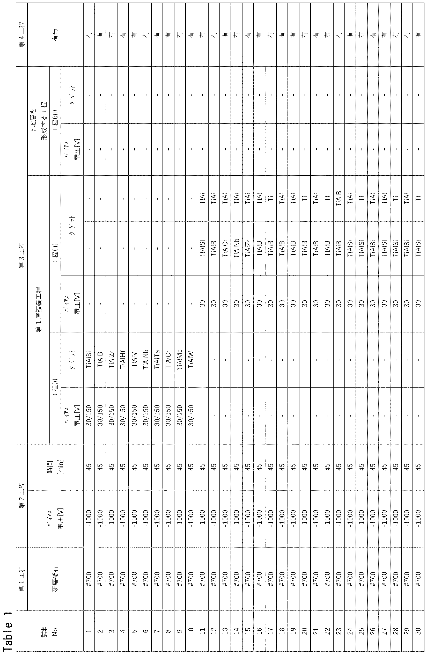
- the outer peripheral surface, the upper surface and the lower surface of the joined body were ground to form a negative land shape (negative land width of 150 ⁇ m and negative land angle of 25°) on the cutting edge. Grinding was performed using a grindstone having a count shown in the "grindstone" column of "first step” in Tables 1 and 2. Thus, a substrate was obtained in which each cutting edge (cutting edge) portion was made of a cubic boron nitride sintered body.
- ⁇ Second step Step of ion bombardment treatment of the surface of the base material>>
- the substrate was set in a vacuum chamber of a film forming apparatus. Next, the inside of the chamber was evacuated. The substrate was then heated to 500° C. while rotating the rotary table at 3 rpm. Next, Ar gas (pressure: 1 Pa) was introduced into the vacuum chamber, the tungsten filament was discharged to generate Ar ions, a bias voltage was applied to the substrate, and the substrate was ion bombarded with the Ar ions. .
- the bias voltage for the ion bombardment treatment and the time for the ion bombardment treatment are as shown in Tables 1 and 2 in the "second step” column "bias voltage" and "time”.
- ⁇ Third step Step of forming a coating on the base material>>
- an arc ion plating method is used to use the target described in the "target” column of the "step of forming the underlayer” in Table 2, and the target in Table 2.
- the step (iii) was performed under the conditions of the bias voltage described in the "Bias Voltage” column of the "Step of Forming Underlayer".
- step (i) the target described in the "target” column of “step (i)” of "first layer coating step” in Tables 1 and 2 , N gas as the reaction gas, and the "bias voltage” column
- the first layer coating step was carried out at the bias voltage described in .
- the description of 30/150 in the "bias voltage” column means that the bias voltage was discontinuously switched between 30V and 150V. More specifically, a bias voltage of 30 V was maintained for 120 seconds, then the bias voltage was switched to 150 V and maintained for 120 seconds, and this cycle was repeated. That is, the time for one cycle was 240 seconds.
- step (ii) two types of targets described in the "target” column of “step (ii)” of “first layer coating step” in Tables 1 and 2 were used, N gas was used as the reaction gas, and "bias The first layer coating step was carried out at the bias voltage given in the "Voltage” column.
- N gas was used as the reaction gas
- bias voltage was 30V.
- the two targets are both "TiAlB" targets.
- sample No. 12 sample no. 101, sample no. 103, and sample no. 104 is common in that a “TiAlB” target and a “TiAl” target are used as two targets, but the composition ratio of the targets is different as follows.
- ⁇ Fourth step Dry blasting the surface of the coating>>
- blasting was performed under the conditions shown in Tables 1 and 2 on the surface to be processed (rake face, flank face, negative land face) of the surface of the coating obtained in the third step.
- the blasting is performed by adjusting the projection angle from about 15 degrees to 70 degrees at a projection distance of 100 mm and blasting for 60 seconds with elastic polishing media using diamond abrasive grains on the rake face, flank face and negative land surface of the coating. was executed under the condition that
- sample No. 1 having the configuration shown in Tables 3 and 4 was obtained. 1 to sample No. 48 and sample no. 101 to sample No. 104 cutting tools were made.
- M “M”, “x max ”, “x min ”, “y max ”, and “y min ” are the terms of “M” and “x max ” in Tables 3 and 4, respectively. Described in the “x min ” term, the “y max ” term, and the “y min ” term. Also, among the obtained results, “a” and “p” are described in the “a” and “p” items in Tables 3 and 4, respectively.
- Sample no. 1 to sample No. 48 corresponds to the example.
- Sample no. 101 to sample No. 104 corresponds to a comparative example. From the results of Tables 3 and 4, sample No. corresponding to the example. 1 to sample No.
- the cutting tool No. 48 is sample No. 48 corresponding to the comparative example. 101 to sample No. It was found to have longer tool life than the 104 cutting tool even in high efficiency machining.
Landscapes
- Chemical & Material Sciences (AREA)
- Engineering & Computer Science (AREA)
- Mechanical Engineering (AREA)
- Chemical Kinetics & Catalysis (AREA)
- Materials Engineering (AREA)
- Metallurgy (AREA)
- Organic Chemistry (AREA)
- Inorganic Chemistry (AREA)
- Cutting Tools, Boring Holders, And Turrets (AREA)
- Physical Vapour Deposition (AREA)
- Drilling Tools (AREA)
Abstract
Description
前記被膜は、第1層を含み、
前記第1層の厚みは、0.2μm以上9μm以下であり、
前記第1層は、Ti(1-x-y)AlxMyNからなり、
前記Mは、ジルコニウム、ハフニウム、周期表5族元素、6族元素、珪素、および硼素からなる群より選択される1種の元素であり、
前記第1層において、前記第1層の厚み方向に沿って、前記x及び前記yは変化し、
前記xの最大値xmaxは、0.20以上0.70以下であり、
前記xの最小値xminは、0以上0.6以下であり、
前記xmaxと前記xminとは、0.01≦xmax-xmin≦0.7を満たし、
前記yの最大値ymaxは、0.01以上0.20以下であり、
前記yの最小値yminは、0以上0.19以下であり、
前記ymaxと前記yminとは、0.01≦ymax-ymin≦0.2を満たす。
近年、高能率加工のニーズが高まっている。これに伴い、高能率加工においても、長い工具寿命を有する切削工具が求められている。
本開示によれば、高能率加工においても長い工具寿命を有する切削工具を提供することが可能である。
最初に本開示の実施態様を列記して説明する。
(1)基材と、前記基材上に配置された被膜と、を備える切削工具であって、
前記被膜は、第1層を含み、
前記第1層の厚みは、0.2μm以上9μm以下であり、
前記第1層は、Ti(1-x-y)AlxMyNからなり、
前記Mは、ジルコニウム、ハフニウム、周期表5族元素、6族元素、珪素、および硼素からなる群より選択される1種の元素であり、
前記第1層において、前記第1層の厚み方向に沿って、前記x及び前記yは変化し、
前記xの最大値xmaxは、0.20以上0.70以下であり、
前記xの最小値xminは、0以上0.6以下であり、
前記xmaxと前記xminとは、0.01≦xmax-xmin≦0.7を満たし、
前記yの最大値ymaxは、0.01以上0.20以下であり、
前記yの最小値yminは、0以上0.19以下であり、
前記ymaxと前記yminとは、0.01≦ymax-ymin≦0.2を満たす。
前記下地層は、前記基材の直上で、且つ、前記第1層の直下に配置され、
前記下地層の厚みは、0.05μm以上1.0μm以下であり、
前記下地層は、TiaAl1-aN又はAlpCr1-pNからなり、
前記aは、0.2以上1.0以下であり、
前記pは、0以上0.8以下であることが好ましい。これによって、切削工具において基材と被膜との密着力が向上する。
本開示の一実施形態(以下、「本実施形態」とも記す。)の切削工具の具体例を、以下に図面を参照しつつ説明する。本開示の図面において、同一の参照符号は、同一部分または相当部分を表すものである。また、長さ、幅、厚み、深さなどの寸法関係は図面の明瞭化と簡略化のために適宜変更されており、必ずしも実際の寸法関係を表すものではない。
図2~図6に示される様に、本実施形態に係る切削工具10は、
基材11と、前記基材11上に配置された被膜40と、を備える切削工具であって、
前記被膜40は、第1層12を含み、
前記第1層12の厚みは、0.2μm以上9μm以下であり、
前記第1層12は、Ti(1-x-y)AlxMyNからなり、
前記Mは、ジルコニウム、ハフニウム、周期表5族元素、6族元素、珪素、および硼素からなる群より選択される1種の元素であり、
前記第1層12において、前記第1層12の厚み方向に沿って、前記x及び前記yは変化し、
前記xの最大値xmaxは、0.20以上0.70以下であり、
前記xの最小値xminは、0以上0.6以下であり、
前記xmaxと前記xminとは、0.01≦xmax-xmin≦0.7を満たし、
前記yの最大値ymaxは、0.01以上0.20以下であり、
前記yの最小値yminは、0以上0.19以下であり、
前記ymaxと前記yminとは、0.01≦ymax-ymin≦0.2を満たす。
本実施形態の基材は、この種の基材として従来公知のものを特に限定なく用いることができる。例えば、上記基材は、超硬合金(例えば、炭化タングステン(WC)基超硬合金、WCの他にCoを含む超硬合金、WCの他にTi、Ta、Nb等の炭窒化物等を添加した超硬合金等)、サーメット(TiC、TiN、TiCN等を主成分とするもの)、高速度鋼、工具鋼、セラミックス(炭化チタン(TiC)、炭化硅素(SiC)、窒化硅素(SiN)、窒化アルミニウム(AlN)、酸化アルミニウム(Al2O3)、サイアロン、およびこれらの混合体等)、立方晶型窒化硼素焼結体(cBN焼結体)、ダイヤモンド焼結体、および結合相中に立方晶型窒化硼素粒子が分散した硬質材料等を挙げることができる。
上記基材の上記被膜と接する面のスキューネスRsksubは、-2以上2以下であることが好ましい。ここで、「スキューネス」とは、JIS B 0601-2001に規定される粗さ曲線のスキューネスを意味し、面の山部と谷部との歪度を示すパラメータである。言い換えれば、「スキューネス」とは、図9および図10で示す様に、平均線L1を中心としたときの山部と谷部との対称性を表す指標である。上記面が平均線L1に対して上側に偏っている場合、「スキューネス」は正の値となる(図9)。また、上記面が平均線L1に対して下側に偏っている場合、「スキューネス」は負の値となる(図10)。また、図9および図10で示す確率密度の分布曲線が正規分布となる場合、スキューネスは「0」となる。
上記基材の被膜と接する面のスキューネスRsksubは、例えば、以下の方法によって求めることができる。先ず、切削工具を、その逃げ面の法線方向に沿い、かつ、刃先を含むように切断して断面を露出させる。切断は、集束イオンビーム装置、又は、クロスセクションポリッシャ装置等を用いることができる。走査型電子顕微鏡(Scanning Electron Microscope:SEM)を用いて、該断面を2000倍で観察して、反射電子像を得る。次いで、画像画像処理ソフト(たとえば、商品名「Winroof」三谷商事株式会社製)を用いて、該反射電子像を2.5倍に拡大することにより、観察視野を得る。次いで、該観察視野において、「被膜の表面」と、「基材の被膜と接する面(基材と被膜との界面に相当)」とを含む50μm四方の矩形の任意の箇所を抜出し、「基材の被膜と接する面」を線としてトレースして抽出する。これによって抽出された線を、画像処理ソフト(たとえば、商品名「Winroof」三谷商事株式会社製)を用いて数値化することにより、該数値の平均値を算出する。ここで、「線を数値化する」とは、抽出された線をx-yの座標軸に置いた場合に、当該線のy軸の値をx軸方向に0.05μm間隔で出力することを意味する。次いで、該平均値に基づいて、基材の被膜と接する面と略平行な方向に平均線を描く。次いで、その該平均線をX軸とし、且つ、該X軸に対する垂直方向をY軸とする座標軸として、上記画像処理ソフトを用いることにより、該座標軸において、被膜の表面における面の粗さ曲線Z(x)を得る。次いで、該Z(x)を以下の式(1)に代入することによって、Rqを得る。ここで、「l」は「50μm」である。

次いで、該Z(x)と該Rqとを以下の式(2)に代入することによって、スキューネスRskを得る。

これを、上記断面における任意の5視野において実行することによって得られた上記スキューネスRskの平均値を算出することにより、上記スキューネスRsksubを求められる。
被膜40は、上記基材11上に配置される(図2~6)。図2~6は、本開示の切削工具の一態様を例示する模式断面図である。「被膜」は、上記基材11の少なくとも刃先部分を被覆することで、切削工具における耐剥離性、耐欠損性、耐摩耗性等の諸特性を向上させる作用を有するものである。ここで記載の刃先部分とは、刃先稜線から基材表面に沿って500μm以内の領域を意味する。上記被膜40は、上記基材11の全面を被覆することが好ましい。しかしながら、上記基材11の一部が上記被膜40で被覆されていなかったり、被膜40の構成が部分的に異なっていたりしていたとしても本実施形態の範囲を逸脱するものではない。
上記被膜の表面のスキューネスRsksurfは、-2以上2以下であることが好ましい。これによって、上記被膜の表面において、山部と谷部の分布の偏りが小さくなることに起因して、加工時の負荷による応力集中が軽減されるため、被膜の耐剥離性を向上することができる。また、上記Rsksurfの下限は、-1.8以上であることがより好ましく、-1.6以上であることが更に好ましく、-1.4以上であることが更により好ましい。また、上記Rsksurfの上限は、1.8以下であることがより好ましく、1.6以下であることが更に好ましく、1.4以下であることが更により好ましい。また、上記Rsksurfは、-1.8以上1.8以下であることがより好ましく、-1.6以上1.6以下であることが更に好ましく、-1.4以上1.4以下であることが更により好ましい。
上記被膜の表面の粗さRasurfは、0μm以上0.1μm以下であることが好ましい。これによって、上記被膜の表面において、凹凸が軽減されることに起因して、加工時の負荷による応力集中が軽減されるため、被膜の耐剥離性を向上することができる。また、上記Rasurfの下限は、0.01μm以上であることが好ましく、0.02μm以上であることがより好ましく、0.03μm以上であることが更に好ましい。また、上記Rasurfの上限は、0.09μm以下であることが好ましく、0.08μm以下であることがより好ましく、0.07μm以下であることが更に好ましい。また、上記Rasurfは、0.01μm以上0.09μm以下であることが好ましく、0.02μm以上0.08μm以下であることがより好ましく、0.03μm以上0.08μm以下であることが更に好ましい。ここで、「表面粗さRa」とは、JIS B 0601-2001に規定される算術平均粗さを意味する。
上記第1層の厚みは、0.2μm以上9μm以下である。これによって、被膜の膜強度を向上することができる。また、上記第1層の厚みの下限は、0.4μm以上であることが好ましく、0.6μm以上であることがより好ましく、0.8μm以上であることが更に好ましい。また、上記第1層の厚みの上限は、8μm以下であることが好ましく、7μm以下であることがより好ましく、6μm以下であることが更に好ましい。また、上記第1層の厚みは、0.4μm以上8μm以下であることが好ましく、0.6μm以上7μm以下であることがより好ましく、0.8μm以上6μm以下であることが更に好ましい。
(分析条件)
一次電子のエネルギー:10keV
電流 :約3nA
入射角度:試料逃げ面の法線に対して0度
分析領域:約10μm×10μm
(イオンスパッタ(Ar+)の条件)
エネルギー :1keV
入射角度 :試料逃げ面の法線に対して約0度
スパッタ速度:約2nm/min
任意の5点について上記測定を実行する。該5点における上記原子濃度比率の測定値の平均から、xmax、ymax、xmin、yminを求められる。また、Mで示される元素の種類も特定することができる。
上記第1層において、結晶子サイズの平均は5nm以上90nm以下であることが好ましい。これによって、結晶子サイズの微細化に起因して、該第1層を含む被膜の膜強度を更に向上することができる。また、結晶子サイズが小さすぎることに起因する第1層の靱性低下を抑制できるため、第1層においてクラックの発生を抑制することができる。また、上記結晶子サイズの平均の下限は、8nm以上であることが好ましく、12nm以上であることがより好ましく、15nm以上であることが更に好ましい。また、上記結晶子サイズの平均の上限は、80nm以下であることが好ましく、70nm以下であることがより好ましく、60nm以下であることが更に好ましい。また、上記結晶子サイズの平均は、8nm以上80nm以下であることがより好ましく、12nm以上70nm以下であることが更に好ましく、15nm以上60nm以下であることが更により好ましい。
γ=Kλ/βcosθ (I)
ここで、Kは形状因子を意味する。また、本明細書においてKは「0.9」である。また、ここで、λはX線波長を意味する。また、ここで、βはピーク半値全幅(Full Width Half Maximum(FWHM))を意味し、ラジアン単位で表される。また、ここで、θは第1層の(200)ピークのブラッグ角を意味する。なお、該測定を任意に選択された5箇所で行う。次いで、5箇所の測定箇所における結晶子サイズの平均値を算出することにより、上記結晶子サイズの平均が求められる。また、上記被膜が表面層(他の層)を含む場合、第1層を露出させた後、上記XRD測定を実行する。
(X線回折測定の条件)
走査軸 :2θ-θ
X線源 :Cu-Kα線(1.541862Å)
検出器 :0次元検出器(シンチレーションカウンタ)
管電圧 :45kV
管電流 :40mA
入射光学系:ミラーの利用
受光光学系:アナライザ結晶(PW3098/27)の利用
ステップ :0.03°
積算時間 :2秒
スキャン範囲(2θ):10°~120°
上記第1層の残留応力は、-3.0GPa以上-0.1GPa以下であることが好ましい。これによって、切削工具の膜強度を更に向上することができる。また、上記第1層の残留応力の下限は、-2.8GPa以上であることが好ましく、-2.5GPa以上であることがより好ましく、-2.2GPa以上であることが更に好ましい。また、上記第1層の残留応力の上限は、-0.2GPa以下であることが好ましく、-0.3GPa以下であることがより好ましく、-0.4GPa以下であることが更に好ましい。また、上記第1層の残留応力は、-2.8GPa以上-0.2GPa以下であることが好ましく、-2.5GPa以上-0.3GPa以下であることがより好ましく、-2.5GPa以上-0.4GPa以下であることが更に好ましい。なお、ここで、残留応力が負の値を示す場合、該残留応力は「圧縮残留応力」を意味する。
上記残留応力は、X線を用いた2θ-sin2ψ法(側傾法)によって求めることが可能である。具体的には、測定条件は下記のとおりである。例えば、第1層の逃げ面上における任意の3点について、X線を用いた2θ-sin2ψ法(側傾法)によって第1層の解析を行い、これら3点で求められた残留応力の平均値を当該第1層における残留応力とする。また、上記被膜が表面層(他の層)を含む場合、第1層を露出させた後、上記XRD測定を実行する。
(測定条件)
管電圧 :45kV
管電流 :200mA
X線源 :Cu-Kα線(1.541862Å)
入射光学系:φ0.3コリメーター
使用したピーク:TiN(2,0,0)
上記第1層の(200)面のX線回折強度I(200)と、上記第1層の(111)面のX線回折強度I(111)と、上記第1層の(220)面のX線回折強度I(220)との合計に対する、上記I(200)の比率I(200)/(I(200)+I(111)+I(220))は、0.50以上であることが好ましい。これによって、被膜の靭性を高めることができ亀裂の伝搬を抑制することができる為、被膜の耐剥離性を更に向上することができる。なお、ここで「(200)面のX線回折強度I(200)」とは、(200)面に由来するX線回折ピークのうち、最も高いピークにおける回折強度(ピークの高さ)(以下、「最大回折強度」とも記す。)を意味する。また、被膜に含まれる2種類以上の化合物のそれぞれについて(200)面に由来するX線回折ピークが存在する場合、すなわち、(200)面に由来するX線回折ピークが異なる位置に複数存在する場合は、「(200)面のX線回折強度I(200)」とは、それらの最大回折強度(ピークの高さ)の合計を意味する。「(111)面のX線回折強度I(111)」及び「(220)面のX線回折強度I(220)」についても同様である。
(X線回折測定の条件)
走査軸 :2θ-θ
X線源 :Cu-Kα線(1.541862Å)
検出器 :0次元検出器(シンチレーションカウンタ)
管電圧 :45kV
管電流 :40mA
入射光学系:ミラーの利用
受光光学系:アナライザ結晶(PW3098/27)の利用
ステップ :0.03°
積算時間 :2秒
スキャン範囲(2θ):10°~120°
上記被膜は、下地層を更に含み、該下地層は、TiaAl1-aN又はAlpCr1-pNからなることが好ましい。この場合、上記下地層は、上記基材の直上で、且つ、上記第1層の直下に配置されることが好ましい。これによって、基材と被膜との密着力を向上することができる。
本実施形態の効果を損なわない限り、上記被膜は、上記他の層を更に含んでいてもよい。図4~図6に示されるように、上記他の層としては、例えば、中間層14、および表面層15等が挙げられる。
本実施形態の被膜は、例えば、隣接する第1層12同士の間(図4)、または隣接する第1層12と表面層15との間(図5)において、中間層14を含むことができる。中間層14は、第1層12と、他の第1層12または第1層12以外の層(表面層15など)との間に配置される層である。また、中間層の組成は、例えば、窒化チタン(TiN)、炭窒化チタン(TiCN)、窒化チタンアルミ(TiAlN)、窒化チタンアルミケイ素(TiAlSiN)、窒化チタンアルミホウ素(TiAlBN)、窒化チタンアルミジルコニウム(TiAlZrN)、窒化チタンアルミハフニウム(TiAlHfN)、窒化チタンアルミバナジウム(TiAlVN)、窒化チタンアルミニオブ(TiAlNbN)、窒化チタンアルミタンタル(TiAlTaN)、窒化チタンアルミクロム(TiAlCrN)、窒化チタンアルミモリブデン(TiAlMoN)、窒化チタンアルミタングステンn(TiAlWN)とすることができる。また、中間層の厚みは、例えば、0.2μm以上1μm以下とすることができる。
本実施形態の被膜は、表面層を含むことができる(図6)。表面層15は、被膜40において最も表面側に配置される層である。ただし、刃先稜線部においては形成されない場合もある。
実施形態1の切削工具の製造方法について以下に説明する。なお、以下の製造方法は一例であり、実施形態1の切削工具は、他の方法で作製されたものでもよい。
上記基材を準備する第1工程(以下、単に「第1工程」という場合がある)と、
上記基材上に上記被膜を形成する第3工程(以下、単に「第3工程」という場合がある)と、を含む。また、該製造方法は、更に、上記第1工程により得られた基材の表面をイオンボンバードメント処理する第2工程(以下、単に「第2工程」という場合がある)、及び/又は、上記第3工程により得られた被膜の表面を乾式ブラスト処理する第4工程(以下、単に「第4工程」という場合がある。)を更に含むことができる。以下、各工程について説明する。
第1工程では、上記基材を準備する。上記基材としては、上述したようにこの種の基材として従来公知のものであればいずれの基材も使用することができる。例えば、形状がISO規格のDNGA150408であり、超硬合金材料(K10相当)からなる基体を準備する。該基体の刃先(コーナー)部分のそれぞれに立方晶窒化硼素焼結体からなるの基材(形状:頂角が55°であり当該頂角を挟む両辺がそれぞれ2mmである二等辺三角形を底面とし、厚みが2mmの三角柱状のもの)を接合することにより接合体を得る。なお接合には、Ti-Zr-Cuからなるロウ材を用いる。次いで、当該接合体の外周面、上面および下面を研削し、刃先にネガランド形状(ネガランド幅が150μmであり、ネガランド角が25°)を形成する。このようにして、刃先(切れ刃)部分がそれぞれ立方晶窒化硼素焼結体からなる基体を得ることができる。
第2工程では、基材の表面をイオンボンバードメント処理する。例えば、先ず、基体を成膜装置の真空チャンバー内にセットする。次いで、チャンバー内の真空引きを行なう。次いで、回転テーブルを3rpmで回転させながら、基体を500℃に加熱する。次いで、真空チャンバー内にArガスを導入し、タングステンフィラメントを放電させてArイオンを発生させ、基体にバイアス電圧を印加し、Arイオンにより、以下の条件で基体のイオンボンバード処理を行なう。
(イオンボンバードメント処理の条件)
Arガスの圧力 :1Pa
基板バイアス電圧:-600V~-1000V
処理時間:10分~45分
これによって、上記Rsksubを-2以上2以下とすることができる。
第3工程では、基材上に被膜を形成する。また、上記第3工程は、上記イオンボンバード処理された基材の表面の少なくとも一部を第1層で被覆する「第1層被覆工程」を含む。
第4工程では、上記第3工程により得られた被膜の表面を乾式ブラスト処理する。例えば、第4工程は、第3工程により得られた被膜のすくい面、逃げ面及びネガランド面に対し、ダイヤモンド砥粒を用いた弾性研磨メディアを、100mmの投射距離で、約15度から70度の投射角度に調整し、60秒~120秒の間ブラストを投射するという条件で、乾式ブラストにより研磨することにより実行される。これによって、被膜の表面の粗さRasurfを0μm以上0.1μm以下とし、且つ、被膜の表面のスキューネスRsksurfを-2以上2以下とすることができる。なお、ブラスト処理を行う面に対する投射角度が70度超の場合、被膜の表面の凹凸と面の粗さとが減少するより、被膜の除去が進行し易いため、被膜の効果を得にくい傾向がある。また、投射角度が15度未満の場合、弾性研磨メディアの研磨効果を得にくいため、被膜の表面の粗さが減少しにくい傾向がある。
本実施形態に係る製造方法では、上述した工程の他にも、例えば、上記第4工程以外の方法により、被膜の表面を処理する工程等を適宜行ってもよい。
[試料No.1~試料No.48、および試料No.1-101~試料No.104]
下記の製造方法を用いて、試料No.1~試料No.48、および試料No.101~試料No.104の切削工具を作製した。
先ず、形状がISO規格のDNGA150408であり、超硬合金材料(K10相当)からなる基体を準備した。次いで、該基体の刃先部分(コーナー部分)に、cBN含有率が70%であり、且つ、結合材の組成がTiN、TiB2、Al2O3、およびAlNからなる組成を有する立方晶型窒化硼素焼結体基材(形状:頂角が55°であり、当該頂角を挟む両辺がそれぞれ2mmである二等辺三角形を底面とし、厚みが2mmの三角柱状のもの)を接合することにより、接合体を得た。なお接合には、Ti-Zr-Cuからなるロウ材を用いた。次いで、該接合体の外周面、上面および下面を研削し、刃先にネガランド形状(ネガランド幅が150μmであり、ネガランド角が25°)を形成した。研削は、表1及び表2の「第1工程」の「研磨砥石」欄に示される番手を有する砥石を用いて、行った。このようにして、刃先(切れ刃)部分がそれぞれに立方晶窒化硼素焼結体からなる基体を得た。

上記基体を成膜装置の真空チャンバー内にセットした。次いで、チャンバー内の真空引きを行なった。次いで、回転テーブルを3rpmで回転させながら、基体を500℃に加熱した。次いで、真空チャンバー内にArガス(圧力:1Pa)を導入し、タングステンフィラメントを放電させてArイオンを発生させ、基体にバイアス電圧を印加し、該Arイオンにより、基体のイオンボンバード処理を行なった。なお、イオンボンバードメント処理のバイアス電圧と、イオンボンバードメント処理の時間とは、表1及び表2の「第2工程」の「バイアス電圧」及び「時間」欄に示す通りである。
<工程(iii):下地層を形成する工程>
次に、試料No.40~試料No.45において、上記基材の表面に下地層を形成するため、アークイオンプレーティング法を用いて、表2の「下地層を形成する工程」の「ターゲット」欄に記載したターゲットと、表2の「下地層を形成する工程」の「バイアス電圧」欄に記載したバイアス電圧との条件で工程(iii)を実行した。
次に、アークイオンプレーティング法を用いて、上記基材または上記下地層の表面に第1層を形成した。試料No.1~試料No.10では、上記工程(i)を行い、試料No.11~No.48、および試料No.101~試料No.104では、上記工程(ii)を行った。
次に、試料No.1~試料No.38、試料No.40~試料No.48、試料No.101~試料No.104を作製するため、第3工程により得られた被膜の表面における被加工面(すくい面、逃げ面、ネガランド面)に対し、表1および表2に記載した条件で、ブラスト処理を実行した。ブラスト処理は、被膜のすくい面、逃げ面及びネガランド面に対し、ダイヤモンド砥粒を用いた弾性研磨メディアを、100mmの投射距離で、約15度から70度の投射角度に調整し、60秒間ブラストを投射するという条件で実行された。
上述のようにして作製した試料No.1~試料No.48、および試料No.101~試料No.104の切削工具を用いて、以下のように、切削工具の各特性を評価した。なお、試料No.1~試料No.48の切削工具は実施例に対応し、試料No.101~試料No.104の切削工具は比較例に対応する。
試料No.1~試料No.48、および試料No.101~試料No.104の切削工具について、第1層におけるTi(1-x-y)AlxMyNの「M」の種類、「xmax」、「xmin」、「ymax」、および「ymin」と、下地層におけるTiaAl1-aN又はAlpCr1-pNの「a」および「p」とを、実施形態1に記載の方法により求めた。得られた結果のうち、「M」、「xmax」、「xmin」、「ymax」、「ymin」を、それぞれ表3および表4の「M」、「xmax」の項、「xmin」の項、「ymax」の項、「ymin」の項に記す。また、得られた結果のうち、「a」、「p」を、それぞれ表3および表4の「a」の項、「p」の項のそれぞれに記す。
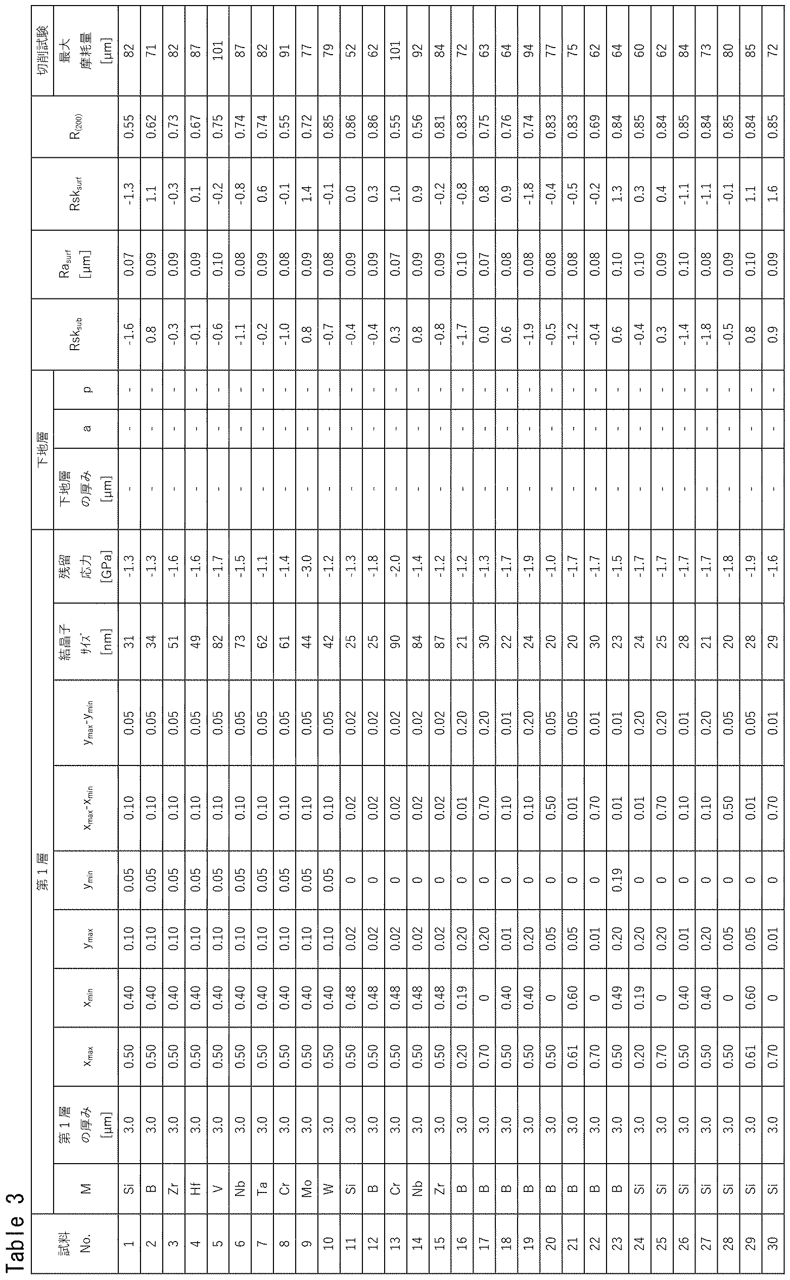
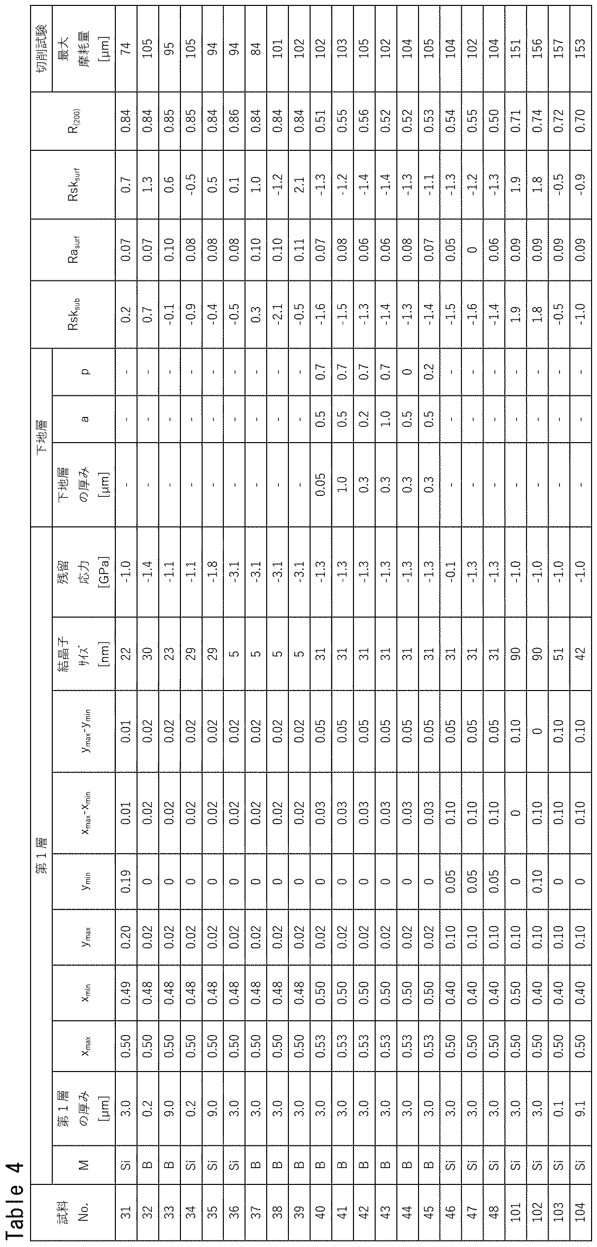
試料No.1~試料No.48、および試料No.101~試料No.104の切削工具について、第1層の厚みを、実施形態1に記載の方法により求めた。得られた結果を、それぞれ表3および表4の「第1層の厚み[μm]」の項に記す。また、試料No.40~試料No.45の切削工具について、下地層の厚みを、実施形態1に記載の方法により求めた。得られた結果を、それぞれ表3および表4の「下地層の厚み[μm]」の項に記す。
試料No.1~試料No.48、および試料No.101~試料No.104の切削工具について、第1層の結晶子サイズの平均を、実施形態1に記載の方法により求めた。得られた結果を、それぞれ表3および表4の「結晶子サイズ[nm]」の項に記す。
試料No.1~試料No.48、および試料No.101~試料No.104の切削工具について、第1層の残留応力を、実施形態1に記載の方法により求めた。得られた結果を、それぞれ表3および表4の「残留応力[GPa]」の項に記す。
試料No.1~試料No.48、および試料No.101~試料No.104の切削工具について、Rsksubを、実施形態1に記載の方法により求めた。得られた結果を、それぞれ表3および表4の「Rsksub」の項に記す。また、試料No.1~試料No.39、および試料No.101~試料No.104の切削工具について、Rasurfを、実施形態1に記載の方法により求めた。得られた結果を、それぞれ表3および表4の「Rasurf[μm]」の項に記す。また、試料No.1~試料No.48、および試料No.101~試料No.104の切削工具について、Rsksurfを、実施形態1に記載の方法により求めた。得られた結果を、それぞれ表3および表4の「Rsksurf」の項に記す。
試料No.1~試料No.48、および試料No.101~試料No.104の切削工具について、第1層のI(200)/(I(200)+I(111)+I(220))を、実施形態1に記載の方法により求めた。得られた結果を、それぞれ表3および表4の「R(200)」の項に記す。
上記のようにして作製した試料No.1~試料No.48、および試料No.101~試料No.104の切削工具を用いて、以下の切削試験を行った。
(切削条件)
被削材 :高硬度鋼SCM415(HRC62)(直径100mm×長さ300mm)
切削速度:V=150m/min.
送り :f=0.2mm/rev.
切込み :ap=0.5mm
湿式/乾式:湿式
当該切削条件は、高能率加工に該当する。
試料No.1~試料No.48は、実施例に該当する。試料No.101~試料No.104は、比較例に該当する。表3および表4の結果から、実施例に該当する試料No.1~試料No.48の切削工具は、比較例に該当する試料No.101~試料No.104の切削工具よりも、高能率加工においても長い工具寿命を有することが分かった。
今回開示された実施の形態および実施例はすべての点で例示であって、制限的なものではないと考えられるべきである。本発明の範囲は上記した実施の形態および実施例ではなく請求の範囲によって示され、請求の範囲と均等の意味、および範囲内でのすべての変更が含まれることが意図される。
Claims (8)
- 基材と、前記基材上に配置された被膜と、を備える切削工具であって、
前記被膜は、第1層を含み、
前記第1層の厚みは、0.2μm以上9μm以下であり、
前記第1層は、Ti(1-x-y)AlxMyNからなり、
前記Mは、ジルコニウム、ハフニウム、周期表5族元素、6族元素、珪素、および硼素からなる群より選択される1種の元素であり、
前記第1層において、前記第1層の厚み方向に沿って、前記x及び前記yは変化し、
前記xの最大値xmaxは、0.20以上0.70以下であり、
前記xの最小値xminは、0以上0.60以下であり、
前記xmaxと前記xminとは、0.01≦xmax-xmin≦0.70を満たし、
前記yの最大値ymaxは、0.01以上0.20以下であり、
前記yの最小値yminは、0以上0.19以下であり、
前記ymaxと前記yminとは、0.01≦ymax-ymin≦0.20を満たす、切削工具。 - 前記第1層において、結晶子サイズの平均は5nm以上90nm以下である、請求項1に記載の切削工具。
- 前記被膜は、下地層を更に含み、
前記下地層は、前記基材の直上で、且つ、前記第1層の直下に配置され、
前記下地層の厚みは、0.05μm以上1.0μm以下であり、
前記下地層は、TiaAl1-aN又はAlpCr1-pNからなり、
前記aは、0.2以上1.0以下であり、
前記pは、0以上0.8以下である、請求項1又は請求項2に記載の切削工具。 - 前記第1層の残留応力は、-3.0GPa以上-0.1GPa以下である、請求項1から請求項3のいずれか1項に記載の切削工具。
- 前記被膜の表面の粗さRasurfは、0μm以上0.1μm以下である、請求項1から請求項4のいずれか1項に記載の切削工具。
- 前記被膜の表面のスキューネスRsksurfは、-2以上2以下である、請求項1から請求項5のいずれか1項に記載の切削工具。
- 前記基材の前記被膜と接する面のスキューネスRsksubは、-2以上2以下である、請求項1から請求項6のいずれか1項に記載の切削工具。
- 前記第1層の(200)面のX線回折強度I(200)と、前記第1層の(111)面のX線回折強度I(111)と、前記第1層の(220)面のX線回折強度I(220)との合計に対する、前記I(200)の比率I(200)/(I(200)+I(111)+I(220))は、0.50以上である、請求項1から請求項7のいずれか1項に記載の切削工具。
Priority Applications (6)
| Application Number | Priority Date | Filing Date | Title |
|---|---|---|---|
| PCT/JP2021/024829 WO2023276067A1 (ja) | 2021-06-30 | 2021-06-30 | 切削工具 |
| KR1020237044614A KR20240011806A (ko) | 2021-06-30 | 2021-06-30 | 절삭 공구 |
| EP21948372.4A EP4364875A1 (en) | 2021-06-30 | 2021-06-30 | Cutting tool |
| JP2022520287A JP7124267B1 (ja) | 2021-06-30 | 2021-06-30 | 切削工具 |
| CN202180099330.9A CN117480023A (zh) | 2021-06-30 | 2021-06-30 | 切削工具 |
| US18/010,235 US11802333B2 (en) | 2021-06-30 | 2021-06-30 | Cutting tool |
Applications Claiming Priority (1)
| Application Number | Priority Date | Filing Date | Title |
|---|---|---|---|
| PCT/JP2021/024829 WO2023276067A1 (ja) | 2021-06-30 | 2021-06-30 | 切削工具 |
Publications (1)
| Publication Number | Publication Date |
|---|---|
| WO2023276067A1 true WO2023276067A1 (ja) | 2023-01-05 |
Family
ID=83004360
Family Applications (1)
| Application Number | Title | Priority Date | Filing Date |
|---|---|---|---|
| PCT/JP2021/024829 Ceased WO2023276067A1 (ja) | 2021-06-30 | 2021-06-30 | 切削工具 |
Country Status (6)
| Country | Link |
|---|---|
| US (1) | US11802333B2 (ja) |
| EP (1) | EP4364875A1 (ja) |
| JP (1) | JP7124267B1 (ja) |
| KR (1) | KR20240011806A (ja) |
| CN (1) | CN117480023A (ja) |
| WO (1) | WO2023276067A1 (ja) |
Citations (11)
| Publication number | Priority date | Publication date | Assignee | Title |
|---|---|---|---|---|
| JPH08119774A (ja) | 1994-10-27 | 1996-05-14 | Sumitomo Electric Ind Ltd | 工具用複合高硬度材料 |
| JP2004074378A (ja) * | 2002-08-22 | 2004-03-11 | Mitsubishi Materials Corp | 高速切削加工で硬質被覆層がすぐれた耐摩耗性を発揮する表面被覆超硬合金製切削工具 |
| JP2004249397A (ja) * | 2003-02-20 | 2004-09-09 | Mitsubishi Materials Corp | 高速重切削条件で硬質被覆層がすぐれた耐摩耗性を発揮する表面被覆超硬合金製切削工具 |
| JP2006334739A (ja) * | 2005-06-03 | 2006-12-14 | Mitsubishi Materials Corp | 耐熱合金の高速切削加工で硬質被覆層がすぐれた耐摩耗性を発揮する表面被覆切削工具 |
| JP2007105839A (ja) * | 2005-10-14 | 2007-04-26 | Mitsubishi Materials Corp | 高硬度鋼の高速切削加工で硬質被覆層がすぐれた耐摩耗性を発揮する表面被覆切削工具 |
| JP2007105841A (ja) * | 2005-10-14 | 2007-04-26 | Mitsubishi Materials Corp | 高反応性被削材の高速切削加工で硬質被覆層がすぐれた耐摩耗性を発揮する表面被覆切削工具 |
| JP2011224688A (ja) * | 2010-04-16 | 2011-11-10 | Mitsubishi Materials Corp | 表面被覆切削工具 |
| WO2017175803A1 (ja) * | 2016-04-07 | 2017-10-12 | 株式会社タンガロイ | 被覆切削工具 |
| JP2019171495A (ja) * | 2018-03-27 | 2019-10-10 | 三菱マテリアル株式会社 | 耐熱亀裂性および耐摩耗性にすぐれた表面被覆切削工具 |
| JP2020151774A (ja) * | 2019-03-18 | 2020-09-24 | 三菱マテリアル株式会社 | 耐熱亀裂性および耐欠損性にすぐれた表面被覆切削工具 |
| WO2021085253A1 (ja) | 2019-10-29 | 2021-05-06 | 三菱マテリアル株式会社 | 表面被覆切削工具 |
Family Cites Families (32)
| Publication number | Priority date | Publication date | Assignee | Title |
|---|---|---|---|---|
| SE526339C2 (sv) * | 2002-09-04 | 2005-08-23 | Seco Tools Ab | Skär med slitstark refraktär beläggning med kompositstruktur |
| EP2308621B1 (en) * | 2004-01-30 | 2015-07-08 | Mitsubishi Materials Corporation | Surface-coated cutting tool made of hard metal |
| DE102004010372A1 (de) * | 2004-03-03 | 2005-09-22 | Gühring, Jörg, Dr. | Werkzeug zum Entgraten von Bohrungen |
| WO2005113175A2 (en) * | 2004-05-21 | 2005-12-01 | Colorado School Of Mines | Functionally graded alumina-based thin film systems |
| SE0402180D0 (sv) * | 2004-09-10 | 2004-09-10 | Sandvik Ab | Deposition of Ti1-xAlxN using Bipolar Pulsed Dual Magnetron Sputtering |
| JP2007313636A (ja) | 2006-04-27 | 2007-12-06 | Kyocera Corp | 切削工具およびそれを用いた被削材の切削方法 |
| US7476064B2 (en) | 2006-04-27 | 2009-01-13 | Kyocera Corporation | Cutting tool and method of cutting workpiece |
| JP5188133B2 (ja) * | 2006-09-27 | 2013-04-24 | 京セラ株式会社 | 切削工具 |
| JP2009028861A (ja) | 2007-07-27 | 2009-02-12 | Kyocera Corp | 切削インサート及びそれを用いた切削工具並びに切削方法 |
| DE102007000512B3 (de) * | 2007-10-16 | 2009-01-29 | Fraunhofer-Gesellschaft zur Förderung der angewandten Forschung e.V. | Hartstoffbeschichtete Körper und Verfahren zu deren Herstellung |
| CN102105249B (zh) * | 2008-07-29 | 2014-01-01 | 京瓷株式会社 | 切削工具 |
| AT509768B1 (de) * | 2010-05-12 | 2012-04-15 | Boehler Schmiedetechnik Gmbh & Co Kg | Verfahren zur herstellung eines bauteiles und bauteile aus einer titan-aluminium-basislegierung |
| JP6024981B2 (ja) * | 2012-03-09 | 2016-11-16 | 三菱マテリアル株式会社 | 高速断続切削加工で硬質被覆層がすぐれた耐チッピング性を発揮する表面被覆切削工具 |
| EP2669401A1 (en) * | 2012-05-29 | 2013-12-04 | Seco Tools AB | Method for depositing a coating and a coated cutting tool |
| CN104858458B (zh) * | 2014-02-26 | 2018-09-14 | 三菱综合材料株式会社 | 耐异常损伤性和耐磨损性优异的表面包覆切削工具 |
| JP6548071B2 (ja) * | 2014-04-23 | 2019-07-24 | 三菱マテリアル株式会社 | 硬質被覆層がすぐれた耐チッピング性を発揮する表面被覆切削工具 |
| US10195676B2 (en) | 2014-08-27 | 2019-02-05 | Kyocera Corporation | Cutting insert, cutting tool, and method of manufacturing machined product |
| EP3000913B1 (en) * | 2014-09-26 | 2020-07-29 | Walter Ag | Coated cutting tool insert with MT-CVD TiCN on TiAI(C,N) |
| JP6709526B2 (ja) * | 2014-10-28 | 2020-06-17 | 三菱マテリアル株式会社 | 表面被覆切削工具 |
| WO2016169935A1 (en) * | 2015-04-20 | 2016-10-27 | Seco Tools Ab | A coated cutting tool and a method for coating the cutting tool |
| KR101963072B1 (ko) * | 2015-11-02 | 2019-03-27 | 스미토모덴키고교가부시키가이샤 | 경질 합금 및 절삭 공구 |
| EP3228726A1 (en) * | 2016-04-08 | 2017-10-11 | Seco Tools Ab | Coated cutting tool |
| US9711367B1 (en) * | 2016-06-01 | 2017-07-18 | Taiwan Semiconductor Manufacturing Co., Ltd. | Semiconductor method with wafer edge modification |
| US11286570B2 (en) * | 2017-01-26 | 2022-03-29 | Walter Ag | Coated cutting tool |
| WO2019065397A1 (ja) * | 2017-09-27 | 2019-04-04 | 三菱日立ツール株式会社 | 被覆切削工具 |
| CN111093873B (zh) | 2017-09-28 | 2021-06-01 | 日立金属株式会社 | 切断工具及其制造方法 |
| CN108446478B (zh) * | 2018-03-14 | 2021-07-06 | 中南大学 | 一种多组元高强度钛合金的设计方法 |
| CN113453828A (zh) * | 2019-02-12 | 2021-09-28 | 三菱综合材料株式会社 | 硬质皮膜切削工具 |
| EP3943222A4 (en) * | 2019-03-22 | 2022-08-03 | MOLDINO Tool Engineering, Ltd. | COATED CUTTING TOOL |
| JP6876278B2 (ja) * | 2019-05-14 | 2021-05-26 | 株式会社タンガロイ | 被覆切削工具 |
| CN114173970B (zh) * | 2019-10-10 | 2024-09-13 | 住友电工硬质合金株式会社 | 切削工具 |
| JP7402666B2 (ja) | 2019-11-28 | 2023-12-21 | 株式会社Lixil | 排水ソケットおよび水洗式便器 |
-
2021
- 2021-06-30 US US18/010,235 patent/US11802333B2/en active Active
- 2021-06-30 JP JP2022520287A patent/JP7124267B1/ja active Active
- 2021-06-30 WO PCT/JP2021/024829 patent/WO2023276067A1/ja not_active Ceased
- 2021-06-30 CN CN202180099330.9A patent/CN117480023A/zh active Pending
- 2021-06-30 EP EP21948372.4A patent/EP4364875A1/en active Pending
- 2021-06-30 KR KR1020237044614A patent/KR20240011806A/ko not_active Ceased
Patent Citations (11)
| Publication number | Priority date | Publication date | Assignee | Title |
|---|---|---|---|---|
| JPH08119774A (ja) | 1994-10-27 | 1996-05-14 | Sumitomo Electric Ind Ltd | 工具用複合高硬度材料 |
| JP2004074378A (ja) * | 2002-08-22 | 2004-03-11 | Mitsubishi Materials Corp | 高速切削加工で硬質被覆層がすぐれた耐摩耗性を発揮する表面被覆超硬合金製切削工具 |
| JP2004249397A (ja) * | 2003-02-20 | 2004-09-09 | Mitsubishi Materials Corp | 高速重切削条件で硬質被覆層がすぐれた耐摩耗性を発揮する表面被覆超硬合金製切削工具 |
| JP2006334739A (ja) * | 2005-06-03 | 2006-12-14 | Mitsubishi Materials Corp | 耐熱合金の高速切削加工で硬質被覆層がすぐれた耐摩耗性を発揮する表面被覆切削工具 |
| JP2007105839A (ja) * | 2005-10-14 | 2007-04-26 | Mitsubishi Materials Corp | 高硬度鋼の高速切削加工で硬質被覆層がすぐれた耐摩耗性を発揮する表面被覆切削工具 |
| JP2007105841A (ja) * | 2005-10-14 | 2007-04-26 | Mitsubishi Materials Corp | 高反応性被削材の高速切削加工で硬質被覆層がすぐれた耐摩耗性を発揮する表面被覆切削工具 |
| JP2011224688A (ja) * | 2010-04-16 | 2011-11-10 | Mitsubishi Materials Corp | 表面被覆切削工具 |
| WO2017175803A1 (ja) * | 2016-04-07 | 2017-10-12 | 株式会社タンガロイ | 被覆切削工具 |
| JP2019171495A (ja) * | 2018-03-27 | 2019-10-10 | 三菱マテリアル株式会社 | 耐熱亀裂性および耐摩耗性にすぐれた表面被覆切削工具 |
| JP2020151774A (ja) * | 2019-03-18 | 2020-09-24 | 三菱マテリアル株式会社 | 耐熱亀裂性および耐欠損性にすぐれた表面被覆切削工具 |
| WO2021085253A1 (ja) | 2019-10-29 | 2021-05-06 | 三菱マテリアル株式会社 | 表面被覆切削工具 |
Non-Patent Citations (1)
| Title |
|---|
| See also references of EP4364875A4 |
Also Published As
| Publication number | Publication date |
|---|---|
| JPWO2023276067A1 (ja) | 2023-01-05 |
| EP4364875A4 (en) | 2024-05-08 |
| JP7124267B1 (ja) | 2022-08-24 |
| US11802333B2 (en) | 2023-10-31 |
| US20230193451A1 (en) | 2023-06-22 |
| CN117480023A (zh) | 2024-01-30 |
| EP4364875A1 (en) | 2024-05-08 |
| KR20240011806A (ko) | 2024-01-26 |
Similar Documents
| Publication | Publication Date | Title |
|---|---|---|
| JP6268530B2 (ja) | 硬質被覆層がすぐれた耐チッピング性を発揮する表面被覆切削工具 | |
| CN102625737B (zh) | 表面被覆切削工具 | |
| CN103249869B (zh) | 涂层切削工具刀片 | |
| JP6394898B2 (ja) | 高速断続切削加工で硬質被覆層がすぐれた耐チッピング性を発揮する表面被覆切削工具 | |
| JP6417959B2 (ja) | 硬質被覆層がすぐれた耐チッピング性を発揮する表面被覆切削工具 | |
| JP6037113B2 (ja) | 高速断続切削加工で硬質被覆層がすぐれた耐チッピング性を発揮する表面被覆切削工具 | |
| JP6992232B2 (ja) | 切削工具 | |
| JP2020040175A (ja) | 被覆切削工具 | |
| KR20180026656A (ko) | 표면 피복 절삭 공구 | |
| JP7355293B2 (ja) | 切削工具 | |
| KR20160078972A (ko) | 표면 피복 질화붕소 소결체 공구 | |
| WO2018070195A1 (ja) | 表面被覆切削工具 | |
| WO2018216256A1 (ja) | 被膜および切削工具 | |
| CN109641283B (zh) | 表面被覆切削工具及其制造方法 | |
| JP2020131424A (ja) | 表面被覆切削工具 | |
| WO2020166683A1 (ja) | 表面被覆切削工具 | |
| JP6690102B2 (ja) | 表面被覆切削工具およびその製造方法 | |
| JP7124267B1 (ja) | 切削工具 | |
| JP7310340B2 (ja) | 被覆切削工具 | |
| JP7338827B1 (ja) | 切削工具 | |
| JP7302628B2 (ja) | 被覆切削工具 | |
| JP7453616B2 (ja) | 表面被覆切削工具 | |
| JP7708333B1 (ja) | 切削工具 | |
| JP7822550B2 (ja) | 表面被覆切削工具 | |
| WO2025196963A1 (ja) | 切削工具 |
Legal Events
| Date | Code | Title | Description |
|---|---|---|---|
| ENP | Entry into the national phase |
Ref document number: 2022520287 Country of ref document: JP Kind code of ref document: A |
|
| 121 | Ep: the epo has been informed by wipo that ep was designated in this application |
Ref document number: 21948372 Country of ref document: EP Kind code of ref document: A1 |
|
| WWE | Wipo information: entry into national phase |
Ref document number: 202180099330.9 Country of ref document: CN |
|
| ENP | Entry into the national phase |
Ref document number: 20237044614 Country of ref document: KR Kind code of ref document: A |
|
| WWE | Wipo information: entry into national phase |
Ref document number: 1020237044614 Country of ref document: KR |
|
| WWE | Wipo information: entry into national phase |
Ref document number: 2021948372 Country of ref document: EP |
|
| NENP | Non-entry into the national phase |
Ref country code: DE |
|
| ENP | Entry into the national phase |
Ref document number: 2021948372 Country of ref document: EP Effective date: 20240130 |