WO2024004731A1 - 電界センサー装置 - Google Patents
電界センサー装置 Download PDFInfo
- Publication number
- WO2024004731A1 WO2024004731A1 PCT/JP2023/022562 JP2023022562W WO2024004731A1 WO 2024004731 A1 WO2024004731 A1 WO 2024004731A1 JP 2023022562 W JP2023022562 W JP 2023022562W WO 2024004731 A1 WO2024004731 A1 WO 2024004731A1
- Authority
- WO
- WIPO (PCT)
- Prior art keywords
- antenna element
- electric field
- field sensor
- sensor device
- voltage
- Prior art date
- Legal status (The legal status is an assumption and is not a legal conclusion. Google has not performed a legal analysis and makes no representation as to the accuracy of the status listed.)
- Ceased
Links
Images

















Classifications
-
- G—PHYSICS
- G01—MEASURING; TESTING
- G01R—MEASURING ELECTRIC VARIABLES; MEASURING MAGNETIC VARIABLES
- G01R29/00—Arrangements for measuring or indicating electric quantities not covered by groups G01R19/00 - G01R27/00
- G01R29/08—Measuring electromagnetic field characteristics
- G01R29/0807—Measuring electromagnetic field characteristics characterised by the application
- G01R29/0814—Field measurements related to measuring influence on or from apparatus, components or humans, e.g. in ESD, EMI, EMC, EMP testing, measuring radiation leakage; detecting presence of micro- or radiowave emitters; dosimetry; testing shielding; measurements related to lightning
-
- H—ELECTRICITY
- H01—ELECTRIC ELEMENTS
- H01Q—ANTENNAS, i.e. RADIO AERIALS
- H01Q1/00—Details of, or arrangements associated with, antennas
- H01Q1/12—Supports; Mounting means
- H01Q1/22—Supports; Mounting means by structural association with other equipment or articles
- H01Q1/24—Supports; Mounting means by structural association with other equipment or articles with receiving set
- H01Q1/248—Supports; Mounting means by structural association with other equipment or articles with receiving set provided with an AC/DC converting device, e.g. rectennas
-
- G—PHYSICS
- G01—MEASURING; TESTING
- G01R—MEASURING ELECTRIC VARIABLES; MEASURING MAGNETIC VARIABLES
- G01R19/00—Arrangements for measuring currents or voltages or for indicating presence or sign thereof
- G01R19/165—Indicating that current or voltage is either above or below a predetermined value or within or outside a predetermined range of values
- G01R19/16566—Circuits and arrangements for comparing voltage or current with one or several thresholds and for indicating the result not covered by subgroups G01R19/16504, G01R19/16528, G01R19/16533
- G01R19/16576—Circuits and arrangements for comparing voltage or current with one or several thresholds and for indicating the result not covered by subgroups G01R19/16504, G01R19/16528, G01R19/16533 comparing DC or AC voltage with one threshold
-
- G—PHYSICS
- G01—MEASURING; TESTING
- G01R—MEASURING ELECTRIC VARIABLES; MEASURING MAGNETIC VARIABLES
- G01R29/00—Arrangements for measuring or indicating electric quantities not covered by groups G01R19/00 - G01R27/00
- G01R29/08—Measuring electromagnetic field characteristics
- G01R29/0864—Measuring electromagnetic field characteristics characterised by constructional or functional features
- G01R29/0878—Sensors; antennas; probes; detectors
-
- G—PHYSICS
- G01—MEASURING; TESTING
- G01R—MEASURING ELECTRIC VARIABLES; MEASURING MAGNETIC VARIABLES
- G01R29/00—Arrangements for measuring or indicating electric quantities not covered by groups G01R19/00 - G01R27/00
- G01R29/12—Measuring electrostatic fields or voltage-potential
-
- G—PHYSICS
- G01—MEASURING; TESTING
- G01R—MEASURING ELECTRIC VARIABLES; MEASURING MAGNETIC VARIABLES
- G01R31/00—Arrangements for testing electric properties; Arrangements for locating electric faults; Arrangements for electrical testing characterised by what is being tested not provided for elsewhere
- G01R31/001—Measuring interference from external sources to, or emission from, the device under test, e.g. EMC, EMI, EMP or ESD testing
-
- G—PHYSICS
- G01—MEASURING; TESTING
- G01V—GEOPHYSICS; GRAVITATIONAL MEASUREMENTS; DETECTING MASSES OR OBJECTS; TAGS
- G01V3/00—Electric or magnetic prospecting or detecting; Measuring magnetic field characteristics of the earth, e.g. declination, deviation
- G01V3/12—Electric or magnetic prospecting or detecting; Measuring magnetic field characteristics of the earth, e.g. declination, deviation operating with electromagnetic waves
-
- G—PHYSICS
- G08—SIGNALLING
- G08C—TRANSMISSION SYSTEMS FOR MEASURED VALUES, CONTROL OR SIMILAR SIGNALS
- G08C19/00—Electric signal transmission systems
-
- H—ELECTRICITY
- H01—ELECTRIC ELEMENTS
- H01Q—ANTENNAS, i.e. RADIO AERIALS
- H01Q9/00—Electrically-short antennas having dimensions not more than twice the operating wavelength and consisting of conductive active radiating elements
- H01Q9/04—Resonant antennas
- H01Q9/16—Resonant antennas with feed intermediate between the extremities of the antenna, e.g. centre-fed dipole
-
- H—ELECTRICITY
- H02—GENERATION; CONVERSION OR DISTRIBUTION OF ELECTRIC POWER
- H02J—ELECTRIC POWER NETWORKS; CIRCUIT ARRANGEMENTS OR SYSTEMS FOR SUPPLYING OR DISTRIBUTING ELECTRIC POWER; SYSTEMS FOR STORING ELECTRIC ENERGY
- H02J50/00—Circuit arrangements or systems for wireless supply or distribution of electric power
- H02J50/001—Energy harvesting or scavenging
-
- H—ELECTRICITY
- H02—GENERATION; CONVERSION OR DISTRIBUTION OF ELECTRIC POWER
- H02J—ELECTRIC POWER NETWORKS; CIRCUIT ARRANGEMENTS OR SYSTEMS FOR SUPPLYING OR DISTRIBUTING ELECTRIC POWER; SYSTEMS FOR STORING ELECTRIC ENERGY
- H02J50/00—Circuit arrangements or systems for wireless supply or distribution of electric power
- H02J50/20—Circuit arrangements or systems for wireless supply or distribution of electric power using microwaves or radio frequency waves
- H02J50/27—Circuit arrangements or systems for wireless supply or distribution of electric power using microwaves or radio frequency waves characterised by the type of receiving antennas, e.g. rectennas
-
- H—ELECTRICITY
- H02—GENERATION; CONVERSION OR DISTRIBUTION OF ELECTRIC POWER
- H02J—ELECTRIC POWER NETWORKS; CIRCUIT ARRANGEMENTS OR SYSTEMS FOR SUPPLYING OR DISTRIBUTING ELECTRIC POWER; SYSTEMS FOR STORING ELECTRIC ENERGY
- H02J7/00—Circuit arrangements for charging or discharging batteries or for supplying loads from batteries
Definitions
- the present technology relates to an electric field sensor device using an antenna device with an energy harvesting function.
- Converting the energy of electromagnetic waves that exist around us into electricity is being considered.
- energy harvesting the current flowing through the antenna into the circuit is rectified into direct current and converted into electrical energy.
- a diode is used to rectify electromagnetic waves into direct current.
- An antenna with a rectifier circuit is called a rectenna.
- Patent Document 1 describes a person detection device using an antenna using a rectenna.
- This person detection device is a detection device that detects a person using fluctuations in electromagnetic waves that are always present in the indoor environment, and includes a current collector that electrically acquires the electromagnetic waves that are always present in the indoor environment, and a current collector that electrically collects the electromagnetic waves that are always present in the indoor environment.
- a rectifier-boosting means that rectifies and boosts the power of electromagnetic waves that are always present in the indoor environment, and a current collection means and the fluctuation factors of the electromagnetic waves that are always present in the indoor environment are determined from changes in the output voltage of the rectifier and booster.
- the structure is designed to find the distance from the human body. Further, the current collecting means and the rectifying and boosting means are operated by the power of electromagnetic waves that are always present in the indoor environment.
- Patent Document 1 uses a planar antenna as an antenna sensor as a current collecting means to detect a human body, but in this case, the antenna size is limited, and the antenna However, because there is only one antenna, there is a problem in that only a very low voltage (mW) can be obtained from the antenna sensor alone, even though the booster circuit and the ground of the measuring instrument function as an antenna.
- mW very low voltage
- the device described in Patent Document 1 mentioned above uses a relatively small copper plate as the current collecting means, so it is only possible to obtain a small AC signal, and it is necessary to use a rectifier booster circuit such as a Cockcroft-Walton circuit. was there. Furthermore, the device described in Patent Document 1 is limited to use in detecting people in indoor environments.
- This technology solves this problem by increasing the antenna size by using a large metal conductor (for example, in cars, laptops, televisions, refrigerators, automatic teller machines, etc.) as one antenna element. This allows a large amount of power to be taken in without using a booster circuit.
- a large metal conductor for example, in cars, laptops, televisions, refrigerators, automatic teller machines, etc.
- Patent Document 1 was limited to indoor environments, but various electric fields such as quasi-electrostatic fields and electromagnetic waves are constantly generated in spaces including outdoors, and this technology applies to such spaces. It also made it possible to capture electric field energy.
- the purpose of this technology is to provide an electric field sensor device that can be applied not only to indoor environments but also to detect metal conductors such as human bodies, living things (animals and plants other than humans), and cars, and can induce large voltages. It's about doing.
- This technology is a dipole that receives an electric field, which has a first antenna element connected or in contact with the ground and a conductor that has a certain resistance value, and a second antenna element that is either grounded or not grounded.
- an antenna device of the structure a rectifier circuit that rectifies a signal induced in the antenna device; and a detection section that detects the level of the output voltage of the rectifier circuit,
- the detection unit detects a change in the output voltage level caused by spatial coupling or contact of the first antenna element or the ungrounded second antenna element with another conductor different from the conductor. It is an electric field sensor device that detects the state and situation of.
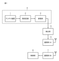
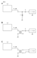
- FIG. 1 is a block diagram of an example of an electric field sensor device according to the present technology.
- 2A, 2B, and 2C are a plan view and a sectional view of an example of an antenna device.
- 3A and 3B are a plan view and a cross-sectional view of another example of the antenna device.
- FIG. 4 is a schematic diagram for explaining the operation of the antenna device.
- 5A, FIG. 5B, and FIG. 5C are schematic diagrams for explaining specific examples of the antenna device.
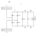
- FIG. 6 is a connection diagram showing an example of the configuration of the electric field sensor device.
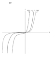
- FIG. 7 is a graph for explaining the characteristics of diodes in the rectifier circuit.
- FIG. 8 is a connection diagram when measuring the output voltage of the rectifier circuit.
- FIG. 1 is a block diagram of an example of an electric field sensor device according to the present technology.
- 2A, 2B, and 2C are a plan view and a sectional view of an example of an antenna device.
- FIG. 9 is a connection diagram of an example of a rectifier circuit using MOSFETs instead of diodes.
- FIG. 10 is a schematic diagram for explaining an example of an electric field sensor device.
- FIG. 11 is a schematic diagram for explaining another example of the electric field sensor device.
- FIG. 12 is a connection diagram showing an example of a configuration for measuring the voltage induced in the electric field sensor device.
- FIG. 13 is a schematic diagram showing an example of a specific configuration for measuring the voltage induced in the electric field sensor device.
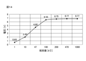
- FIG. 14 is a graph showing changes in voltage with respect to the value of ground resistance of the electric field sensor device.
- FIG. 15 is a connection diagram of an example of a high-pass filter connected to a ground wire.
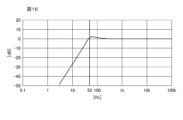
- FIG. 16 is a graph showing frequency characteristics of an example of a high-pass filter.
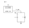
- FIG. 17 is a connection diagram of an example of a parallel resonant circuit connected to a ground wire.
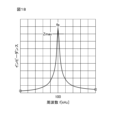
- FIG. 18 is a graph showing frequency characteristics of an example of a parallel resonant circuit.
- FIG. 19 is a connection diagram showing a configuration in which a high-pass filter and a parallel resonant circuit are combined.
- 20A, 20B, and 20C are block diagrams showing multiple circuit examples.
- FIG. 21 is a connection diagram showing an example of configuring two antenna elements separated by a resistor.
- FIG. 22 is a connection diagram showing an example of configuring two antenna elements separated by a filter.
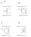
- 23A, 23B, 23C, and 23D are connection diagrams showing multiple examples of filters.
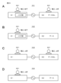
- FIG. 24A, 24B, 24C, and 24D are schematic diagrams showing four configuration examples of an electric field sensor device according to the present technology.
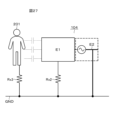
- FIG. 25 is a schematic diagram showing the configuration of an embodiment in which the present technology is applied to a human sensor.
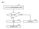
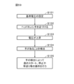
- FIG. 26 is a flowchart used to explain the operation of the human sensor shown in FIG. 25.
- FIG. 27 is a schematic diagram showing another configuration example of the embodiment in which the present technology is applied to a human sensor.
- FIG. 28 is a schematic diagram showing the configuration of an embodiment in which the present technology is applied to a vehicle sensor.
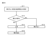
- FIG. 29 is a flowchart used to explain the operation of the vehicle sensor shown in FIG. 28.
- FIG. 30 is a schematic diagram showing the configuration of an embodiment in which the present technology is applied to a human sensor using a fluorescent lamp device.
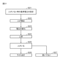
- FIG. 31 is a flowchart used to explain the operation of the human sensor shown in FIG.
- FIG. 32 is a schematic diagram showing the configuration of an embodiment in which the present technology is applied to a human sensor for a warm water-cleaning toilet seat.
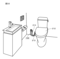
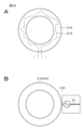
- FIGS. 33A and 33B are schematic diagrams showing the configuration of another embodiment in which the present technology is applied to a human sensor for a warm water-cleaning toilet seat.
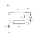
- FIG. 34 is a schematic diagram showing the configuration of still another embodiment in which the present technology is applied to a human sensor for a warm water-cleaning toilet seat.
- FIG. 35 is a flowchart used to explain the operation of the human sensor shown in FIG.
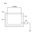
- FIG. 36 is a schematic diagram showing the front side of the configuration of an embodiment in which the present technology is applied to a person sensor of an automatic teller machine.
- FIG. 37 is a schematic diagram showing an aspect of the configuration of an embodiment in which the present technology is applied to a person sensor of an automatic teller machine.
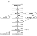
- FIG. 38 is a flowchart used to explain the operation of the human sensor shown in FIGS. 36 and 37.
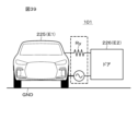
- FIG. 39 is a schematic diagram showing the configuration of an embodiment in which the present technology is applied to a person sensor for a car door.
- FIG. 40 is a cross-sectional view showing an example of the configuration of a part of FIG. 39.
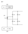
- FIG. 41 is a partial connection diagram of the circuit portion of the configuration shown in FIG. 39.
- FIG. 42 is a flowchart used to explain the operation of the human sensor shown in FIGS. 39, 40, and 41.
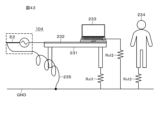
- FIG. 43 is a schematic diagram showing the configuration of an embodiment in which the present technology is applied to a human sensor in an office.
- 44A and 44B are schematic diagrams used to explain the human sensor shown in FIG. 43.
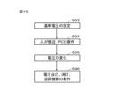
- FIG. 45 is a flowchart used to explain the operation of the human sensor shown in FIGS. 43, 44A, and 44B.
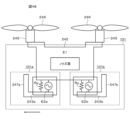
- FIG. 46 is a schematic diagram showing the configuration of an embodiment in which the present technology is applied to an unmanned aircraft.
- FIG. 47 is a simplified diagram showing the configuration of FIG. 46.
- FIG. 48 is a schematic diagram showing a modification of the configuration of FIG. 47.
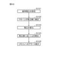
- FIG. 49 is a flowchart used to explain the operation of the sensor of the unmanned aircraft shown in FIGS. 47 and 48.
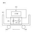
- FIG. 50 is a schematic diagram showing the configuration of an embodiment in which the present technology is applied to a transfer robot.
- FIG. 51 is a schematic diagram showing a modification of the configuration of FIG. 50.
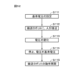
- FIG. 52 is a flowchart used to explain the operation of the sensor shown in FIGS. 50 and 51.
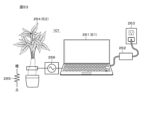
- FIG. 53 is a schematic diagram showing the configuration of an embodiment in which the present technology is applied to a human sensor using a potted plant.
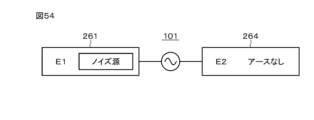
- FIG. 54 is a schematic diagram used to explain the human sensor shown in FIG. 53.
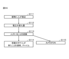
- FIG. 55 is a flowchart used to explain the operation of the human sensor shown in FIGS. 53 and 54.
- FIG. 56 is a flowchart used to explain the operation when the configuration shown in FIGS. 53 and 54 is used as a water supply state sensor.
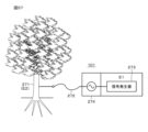
- FIG. 57 is a schematic diagram showing the configuration of an embodiment in which the present technology is applied to a sensor for underground moisture content.
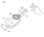
- FIG. 58 is a schematic diagram showing the configuration of an embodiment in which the present technology is applied to a hand sensor for controlling the operation of headphones.
- FIG. 59 is a flowchart used to explain the operation of the hand sensor shown in FIG. 58.
- a quasi-electrostatic field is a voltage phenomenon that does not propagate like a radiated electromagnetic field, so-called radio waves, and is distributed like an electrostatic charge near people, vehicles, and substances. While an electrostatic field is considered to have no time change, a quasi-electrostatic field has a frequency component and is accompanied by a time change.
- Ground refers to the connection or contact between a conductor and a human body, a living thing (animals and plants other than humans), or a metal part of a product when the conductor exists in space with a certain potential. A voltage change is induced depending on the condition. By detecting these changes, we can determine the presence (distance) of conductors that are connected to or in contact with the human body, living things (animals and plants other than humans), cars, bicycles, trains, etc., and the type of conductor (whether a person is approaching or not). This makes it possible to detect whether a car is approaching, etc.).
- FIG. 1 is a block diagram schematically showing an electric field sensor device according to the present technology.
- An energy collecting section (hereinafter appropriately referred to as a harvester) 4 including an antenna device 1, a rectifier circuit 2, and a power storage section 3 is provided.
- the harvester 4 is a device that extracts electric field energy existing in space from metal and outputs the energy as electric power.
- the harvester 4 includes an antenna device 1 as a current collector, a rectifier circuit 2, and a power storage unit 3 that smoothes and stores the output of the rectifier circuit 2.
- the output voltage obtained from the power storage unit 3 is supplied to the detection unit 5.
- the detection unit 5 detects a change in the voltage supplied from the harvester 4 and generates a sensor output.
- the detection unit 5 is composed of an A/D converter, a microcomputer, and the like.
- the sensor output output from the detection section 5 is supplied to the communication section 6(A).
- the communication section (A) 6 transmits the sensor output to another communication section (B) 7 by wireless or wired communication.
- the sensor output received by the communication section (B) 7 is supplied to the control section 8 .
- the control unit 8 controls the target device according to the sensor output. Note that the detection unit 5 is connected to the downstream of the communication unit (B) 7, and the voltage output from the power storage unit 3 is converted into digital data and supplied to the communication unit, and the received digital data is judged by the detection unit. It's okay.
- the antenna device 1 will be explained. Electric fields exist in the metal parts (iron, aluminum, copper, metal alloys, etc.) of industrial products that exist around us, such as cars, vending machines, refrigerators, microwave ovens, metal racks, guardrails, mailboxes, traffic lights, etc. Energy is induced. Using such a metal part of the product as an antenna, it is possible to collect the electric field energy of radio waves and quasi-electrostatic fields (near field) in space. In other words, if a metal exists in an electrically floating state, alternating current power (alternating current) of various frequencies is flowing on the metal surface, so this metal can be regarded as an antenna and this power can be absorbed. It can be efficiently converted into energy. Note that the product metal part is a metal part other than an industrial product designed as an antenna.
- the antenna device 1 of the harvester 4 has a dipole structure composed of two antenna elements.
- the first antenna element is used for cars, refrigerators, televisions, notebook computers (hereinafter referred to as notebook PCs), unmanned aerial vehicles (hereinafter referred to as drones), automatic teller machines (hereinafter referred to as ATMs), etc. It is a metal part of a product such as a train or a conductor that is electrically connected to the metal part of the product.
- the second antenna element is an electrode, a copper foil pattern, a coil, etc. configured on the substrate. Furthermore, by connecting to the ground with a cable, the coupling with the ground can be strengthened, and the voltage generated by the antenna device can be increased.
- a first antenna element an antenna element that comes into contact with or is connected to a product metal part that is a conductor
- a second antenna element an antenna element that is not in contact with or connected to a product metal part
- FIGS. 2A plan view
- FIG. 2B sectional view
- FIG. 2C cross section
- FIG. 2B cross-sectional view
- a plate-shaped (patch-shaped) conductive member 11 is provided as a first antenna element that contacts or is connected to the metal part of the product. .
- the conductive member 11 is a plate-shaped member made of a conductor such as gold, silver, aluminum, copper, iron, nickel, or an alloy.
- the contact surface of the conductive member 11 with the metal may be coated with a resin.
- the conductive member 11 has a shape such as a line, a pin, a hemisphere, or an uneven shape, depending on the shape of the metal part of the product.
- the metal part of the product and the conductive member 11 are brought into contact or connected by a method such as welding, mechanical coupling (such as caulking), adhesion with a conductive adhesive, or attachment to a steel material using magnetism such as a magnet.
- the conductive member 11 for example, conductive resin or conductive rubber containing carbon, metal, etc. may be used.
- conductive resin for example, electrodes of various shapes can be easily formed.
- conductive rubber it is possible to construct electrodes that can be elastically deformed, electrodes that have high adhesion, and the like.
- the material of the conductive member 11 is not limited, and the above-mentioned materials may be used alone, or the electrodes may be constructed by combining each material.
- a plate-shaped (patch-shaped) conductive member 11 and a device board (circuit board) 12 including a copper foil pattern as a second antenna element are arranged facing each other, and the conductive member 11 and the device A dielectric plate 13 is interposed between the substrates 12 .
- a space may be provided between the conductive member 11 and the device board 12 without providing the dielectric plate 13.
- the antenna device 1 is constituted by the conductive member 11 and the ground electrode 19 formed by the copper foil pattern of the device board 12. Ground electrode 19 is the second antenna element.
- the antenna device 1 has a T-shaped antenna structure in which a flat plate is used as an antenna element. The connection portion between the signal path electrode of the device board 12 and the conductive pin 14 becomes the feeding point 15 of the antenna.
- a circuit section 16 is provided on, for example, the back surface of the device board 12.
- Circuit section 16 includes rectifier circuit 2 and power storage section 3 shown in FIG. Furthermore, the detection section 5 and the communication section 6 may be configured as the circuit section 16.
- the antenna device configured as described above is housed within the case 17.
- the contact surfaces of the case 17 other than the conductive member 11 are made of an insulating material such as resin.
- the sides of the case other than the contact surface with the metal that absorbs energy, the opposite side of the case, etc. are made of insulating material.
- FIG. 2C shows a configuration in which the case 17 is composed of a case 17A made of non-metal such as resin and a case 17B made of metal. It is also possible to adopt a configuration in which the ground electrode 19 on either the upper or lower surface of the device board 12 and the case 17B are electrically connected. That is, the case 17A made of an insulating material on which the conductive member 11 is provided and the case 17B made of a metal material constituting the opposite side thereof are connected by a connecting part 22 such as a screw, and the ground electrode of the case 17B and the equipment board 12 is connected. 19 may be connected by a wire 23.
- an insulated coated cable 24 is further connected to the ground electrode 19 formed of a copper foil pattern on the device board 12 with solder or the like, so as to be grounded to the ground. It's okay.
- the conductive member 11 described above is configured in a plate shape and is configured to be in contact with or connected to the metal part of the product.
- the power feeding point 15 may be connected directly to the metal part of the product using an insulated coated cable or the like.
- the conductive member 11 of the antenna device 1 described above is brought into contact with the metal part of the product.
- a conductive member 11 is attached to the metal part of the product.
- the antenna device 1 can capture energy from both a quasi-electrostatic field such as leakage current, such as noise, and radio waves, such as broadcast waves.
- the conductive member 11 is directly connected to the metal part of the product, but in the above-mentioned example, the structure is basically such that the conductive member 11 makes surface contact to increase the capacitance. If it is in contact with or connected to a metal part, in the case of contact, it may be a pin structure, hemispherical, or uneven fitting structure in addition to the planar shape, and in the case of connection, it may be screwed, soldered, They may be connected directly by welding or the like, or via an insulator (or air) such as an insulated cable or conductive rubber.
- Electric field energy can be received and electric power can be generated by the antenna device 1 configured by the conductive member 11 in contact with metal and the ground electrode 19 of the device board 12, or a separate electrode. Note that in the case where the conductive member 11 is capacitively coupled to metal even with a space or an insulator interposed therebetween, the size of the first antenna element can be increased.
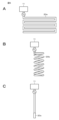
- FIGS. 5A, 5B and 5C Other rows of second antenna elements formed on the substrate are shown in FIGS. 5A, 5B and 5C.
- FIG. 5A shows the configuration of the meander antenna 20a
- FIG. 5B shows the configuration of the coil 20b.
- the coil 20b may be configured as a chip coil.
- FIG. 5C shows a configuration having an inductor 20c at the tip. These configurations can reduce the occupied area and increase the antenna length, thereby increasing the induced voltage.
- the second antenna element may be configured as a plate-shaped antenna having a wide band, and can be used in combination with the illustrated antennas or in combination with the above-described antennas as appropriate.
- FIG. 4 An example of the configuration of the harvester 4 is shown in FIG.
- a full-wave rectifier circuit can increase the voltage of the AC signal and capture all of it, so it is preferable to use a full-wave rectifier circuit even if you include the loss of the diode in the diode used for rectification.
- the rectifier circuit 2 a half-wave rectifier circuit, a voltage doubler circuit, a Cockcroft-Walton circuit, etc. may be used.
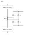
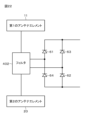
- diodes 61 and 64 are connected in series, and diodes 63 and 62 are connected in series.
- a connection point between the anode of the diode 61 and the cathode of the diode 64 is connected to the conductive member 11, and a connection point between the anode of the diode 63 and the cathode of the diode 62 is connected to the ground electrode 19 as a second antenna element.
- a connection point between the cathode of the diode 61 and the cathode of the diode 63 is connected to one output terminal 34a, and an anode of the diode 64 and an anode connection point of the diode 62 are connected to the other output terminal 34b.
- An electrostatic countermeasure varistor 66 (for example, a Zener diode) is connected in parallel between the output terminals 34a and 34b.
- a power storage unit (capacitor) 3 is connected in parallel between output terminals 34a and 34b. Output terminals 35a and 35b are led out from both ends of power storage unit 3, and detection unit 5 is connected between output terminals 35a and 35b.
- FIG. 7 and Table 1 show the results of measuring the forward voltage Vf and reverse current Is of the diode used in the rectifier circuit 2.
- a silicon and germanium diode with product number 1N60 was measured, and the other product number ISS108 was evaluated using a germanium diode made by a different manufacturer.
- a curve 42 is a characteristic of 1N60 (silicon)
- a curve 41 is a characteristic of 1N60 (germanium)
- a curve 43 is a characteristic of ISS 108 (germanium).
- the current that flows when a voltage is applied in the reverse direction of the diode is the reverse current Is.
- the measured data in Table 1 is when 10V is applied in the opposite direction of the diode.
- the forward voltage Vf is the voltage at which a forward current (1 mA) begins to flow through the diode.
- a diode 1N60 that does not allow current to flow in the reverse direction can take in more power than a diode with a low voltage at which current begins to flow in the forward direction. Do you get it. Since the input to be rectified is alternating current, the reverse current Is when the forward voltage Vf of the diode is applied in the reverse direction is 10V in Table 1, so the same voltage as Vf is applied in the reverse direction. Calculating the reverse direction current Is when 1N60 (silicon) is 0.036 ⁇ A, 1N60 (germanium) is 0.21 ⁇ A, and ISS108 (germanium) is 0.5 ⁇ A.
- the ratio of forward current (1 mA)/reverse current Is at forward voltage Vf is calculated to be 1/27778 for 1N60 (silicon) and 1/4762 for 1N60 (germanium), ISS108 (germanium) is 1/2000th. That is, the diode used in the rectifier circuit 2 needs to have the above-mentioned ratio greater than about 4,700 times, and preferably, the above-mentioned ratio is 10,000 or more. As a result, among the three diodes cited as examples, 1N60 (silicon) has the most suitable characteristics.
- a full-wave rectifier circuit (consisting of diodes 61 to 64 and Zener diodes 66 and 67) is connected to the antenna device 1, and the output voltage of the full-wave rectifier circuit is connected to a high resistance (2 M ⁇ or more, preferably The voltage can be measured by a sensor such as a voltmeter 95 (10 M ⁇ ). Further, a battery 96 is charged by the output of the full-wave rectifier circuit via the reverse current prevention diode 65, and the output of the battery 96 is used as a power source for the voltmeter 95.
- a MOS (Metal Oxide Semiconductor) FET is used as a switching element instead of a diode.
- Field Effect Transistor can be used. That is, a rectifier circuit is constituted by four FETs 61a, 62a, 63a, and 64a, a backflow prevention diode 65a, and a FET protection Zener diode 67a.
- the FETs 61a and 63a are P-channel depletion type MOSFETs, and when a negative voltage is applied to the gate, current flows from the drain to the source.
- the FETs 62a and 64a are N-channel depletion type MOSFETs, and when a positive voltage is applied to the gate, current flows from the drain to the source.
- the drain of FET 61a and the drain of FET 64a are connected to each other, and the drain of FET 62a and the drain of FET 63a are connected to each other.
- the gates of FETs 62a and 63a and the connection points of the drains of FET 61a and FET 64a are connected to antenna element 11. Connection points between the gates of FETs 61a and 64a, the drains of FET 62a, and the drains of FET 63a are connected to antenna element 20.
- the FET 62a is OFF, the FET 63a is ON, the FET 61a is OFF, and the FET 64a is ON.
- the source connection point of the FET 61a and the source of the FET 63a are connected to one output terminal 34a via a backflow prevention diode 65a.
- the source connection point of the FET 62a and the source of the FET 64a are connected to the other output terminal 34b.
- a Zener diode 67a for FET protection is connected between the output terminal 34a and the output terminal 34b.
- the four FETs 61a, 62a, 63a, and 64a may be configured discretely or may be configured using a dedicated IC.
- a rectifier circuit using FETs the conductivity type (N channel/P channel) of each FET may be exchanged.
- a rectifier circuit using FETs can be used instead of the above-described rectifier circuit using diodes, and the same effects as the embodiment and its modifications can be obtained.
- FETs when the frequency to be harvested is a low frequency such as 50 Hz, FETs have better conversion efficiency than diodes, so they may be used depending on the frequency of the equipment to be harvested.
- the antenna device 1 of the harvester 4 has a dipole structure composed of two antenna elements. That is, the antenna device 1 is configured by a product metal part or a first antenna element that contacts or is connected to the product metal part, and a second antenna element that does not contact or connect to the product metal part.
- the first antenna element is a metal part of a product such as a car, a refrigerator, a television receiver, a notebook PC, a drone, an ATM, a train, or the like, or an antenna element that contacts or is connected to the metal part of the product.
- the second antenna element is an electrode, a copper foil pattern, a coil, etc. configured on the substrate.
- an electric field sensor device is configured by a harvester 4 including such an antenna device 1.
- FIGS. 10 and 11 are diagrams schematically showing one example and other examples of the electric field sensor device.
- a grounding resistor Rx is inserted between the first antenna element E1 (hereinafter simply referred to as antenna element E1) corresponding to the conductive member 11 of the antenna device 1 described above and the ground (earth).
- the ground resistance Rx has a value of 10 k ⁇ or more, as described later.
- the second antenna element E2 (hereinafter simply referred to as antenna element E2) corresponding to the ground electrode 19, copper foil pattern, meander antenna on the board, etc. of the antenna device 1 described above is not grounded.
- the antenna element E2 is capacitively coupled to the ground (earth).
- An electric field sensor device 101 having the configuration shown in FIG. 1 and including an antenna device consisting of antenna elements E1 and E2 is schematically represented as shown in FIG.
- the voltage induced by antenna element E1 and antenna element E2 is represented by a voltage source.
- the electric field sensor device 102 shown in FIG. 11 has a configuration in which the antenna element E2 is connected to the ground.
- the antenna element E1 may have a noise source or may not have a noise source.
- Electric field sensor devices 101 and 102 shown in FIGS. 10 and 11 respectively have a noise source.
- the noise source refers to a source that generates noise with a frequency of several Hz to 1 MHz, which is included in the metal part of the product. Such noise is generated from switching power supplies, motors, etc. Even when such a noise source does not exist, various electric fields such as quasi-electrostatic fields and electromagnetic waves are always generated in space, and the output voltage of the harvester is generated by the electric field energy in such space.
- the antenna element E2 which is not in contact with or connected to the metal part of the device that is a conductor, is not grounded, so the antenna element E2 can function as a sensor. Further, the antenna element E1 side can also function as a sensor. That is, one of the antenna elements E1 and E2 can function as a sensor.
- the antenna element E2 is grounded, so the antenna element E2 does not function as a sensor.
- Antenna element E1 functions as a sensor.
- the antenna element that is not on the sensor side is connected to the ground or something that connects to the ground using a coated cable or the like, it may be routed close to the detection target, depending on the dielectric constant of the coated cable.
- FIGS. 12 and 13 are schematic diagrams showing a measuring device for measuring the relationship between the output of the harvester 4 and the ground resistance.
- FIG. 14 is a graph showing the relationship between the output of the harvester device and the ground resistance.
- a test harvester 4 (see FIG. 6) are connected.
- a resistive element 116 is connected between the input terminals of the harvester 4 .
- the device 110 is used as an antenna element E1
- the power tap 113 is used as an antenna element E2.
- One input terminal of the harvester 4 is connected to the ground terminal 111 of the device 110, and the other input terminal is connected to the GND 114.
- output terminals 115a and 115b of a power tap 113 are connected to two power terminals 112a and 112b provided on the device 110, respectively, and AC 100V is supplied thereto.
- a resistive element 116 is connected between the input terminals of the harvester 4 .
- the resistance element 116 is an element such as a wire-wound resistance to which a predetermined DC resistance value is set.
- Resistance element 116 functions as a ground resistance that connects device 110 and GND 114. For example, if the resistive element 116 is sufficiently large, the device 110 will be in a substantially floating state with respect to the GND 114.
- the output voltage of the harvester 4 (the voltage between the output terminals) is measured by changing the DC resistance value of the resistance element 116.
- the graph shown in FIG. 14 shows the output voltage [V] detected by the harvester 4 when the DC resistance value [ ⁇ ] of the resistance element 116 serving as the ground resistance is changed.
- the detected voltage was 0.60V.
- the DC resistance value was 10 k ⁇ , a voltage of 2.00 V was detected, and when the DC resistance value was 47 k ⁇ , a voltage of 4.60 V was detected.
- the higher the DC resistance value the closer the ground of the device 110 serving as the antenna element E1 is to the floating state with respect to the ground GND 114, and the higher the detected voltage becomes.
- the detected voltage becomes 6.55V when it reaches 100 k ⁇ , for example. This is approximately the same value (6.77V) when the resistive element 116 is removed and the ground of the device 110 is completely floated. That is, by inserting the resistive element 116 having a DC resistance of about 100 k ⁇ , the antenna element E1 becomes substantially floating with respect to the ground, and the harvester 4 induces a voltage without any problem. Note that even if the DC resistance is in the range of 100 k ⁇ or less, it is possible to induce a voltage of 2.00 V or more if the resistance value is, for example, 10 k ⁇ or more.
- the DC resistance component of the grounding resistance is described.
- the electric field energy taken in by the harvester 4 is mainly the energy of the alternating current signal. Therefore, for example, if the resistance (impedance) to an AC signal of a target frequency is sufficiently large, it becomes possible to bring the ground of the device 110 close to a floating state at that frequency, and it becomes possible to induce a high voltage. Specifically, it is possible to use an inductance such as a coil.
- the 50 Hz (or 60 Hz) AC signal when connected to a 50 Hz (or 60 Hz) AC power source, the 50 Hz (or 60 Hz) AC signal is considered to be the main source of electric field energy. For this reason, for example, when the impedance at 50 Hz (or 60 Hz) is 10 k ⁇ or more, the ground of the device 90 becomes substantially floating, as described above, and it becomes possible to take in energy efficiently.
- safety standards may require that it be grounded as a measure against electric leakage to prevent electric shock to the human body. In this case, all the energy induced in the device 110 escapes to ground, and no voltage is induced.
- D-grounding is grounding work performed on low-voltage machines and appliances of 300V or less, metal outer boxes, and metal pipes.
- D-grounding is used for equipment that requires grounding among devices that are connected to a 100V AC power source.
- the grounding of devices such as microwave ovens, refrigerators, washing machines, dryers, air conditioners, dehumidifiers, various measuring instruments, factory robots, and server devices conform to this standard. In this way, when targeting general equipment, D grounding becomes the standard.
- the equipment to which the harvester 4 is applied is D-grounded.
- D grounding a grounding resistance with a DC resistance of 100 ⁇ or less is required.
- a grounding resistor with a DC resistance of 500 ⁇ or less. It's okay. For example, if there is a mechanism to cut off the power supplied to equipment when dark current is detected, changing the grounding resistance from 100 ⁇ to 500 ⁇ for D grounding is permitted.
- the 50Hz (or 60Hz) AC signal when connected to a low AC power source such as 50Hz (or 60Hz), the 50Hz (or 60Hz) AC signal may be considered to be the main source of electric field energy.
- the inductance of the coil alone would have a very large value, making it difficult to create a state where the coil alone is floating in space. In other words, the inductance value becomes several hundred H, which is not realistic.
- a high-pass filter structure 121 (Chebyshev high-pass filter) as shown in FIG. 15 can be considered.
- the output terminal of the high-pass filter 121 is open.
- the front stage of the filter contains a coil, so by setting the DC resistance value of the coil in this part to meet safety standards, high impedance (100 k ⁇ or more) can be achieved for 50 Hz (or 60 Hz) AC signals. It becomes possible to realize this. As a result, the inductance of the coil can be reduced even at low frequencies, and miniaturization can also be achieved. For example, when configuring this filter at 50 Hz, the inductance of the coil is 22 mH, the capacitance of the capacitor is 470 ⁇ F, and the DC resistance of the coil is 22 ⁇ .
- the frequency characteristics of this high-pass filter 121 are as shown in FIG.
- the capacitance of a capacitor has a frequency component, and even if it shows a high value at 50 Hz (or 60 Hz), it decreases at frequencies of 1 kHz or higher. Therefore, if a frequency component higher than that is induced in the device 110 as electric field energy, the high-pass filter structure 121 alone will not be able to harvest that energy.
- the frequency components of the electric field energy induced in the device 110 are investigated in advance, and at that frequency, the It is also possible to configure parallel resonant circuit 122 between the earth wire and ground.
- the parallel resonant circuit 122 Since the parallel resonant circuit 122 has a configuration in which a coil and a capacitor are inserted in parallel, it has a high impedance at the frequency of the electric field energy induced in the device 110 and desired to be harvested, and has a high impedance with respect to direct current because it is the direct current resistance of the coil. It is configurable in a way that meets the criteria. For example, as shown in FIG. 18, when configuring a parallel resonant circuit 122 having the characteristic that the impedance is maximum at 100 kHz, the inductance of the coil is 10 mH, the capacitance of the capacitor is 0.5 ⁇ F, and the DC resistance of the coil is: It is 0.04 ⁇ .
- the parallel resonant circuit 122 is desirably configured with an electrolytic capacitor because the higher the Q value, the wider the frequency range with high impedance.
- the high-pass filter 121 and the parallel resonant circuit 122 By combining the high-pass filter 121 and the parallel resonant circuit 122 (at least one or more), electric field energy tailored to various frequency components induced in the device 110 can be generated while satisfying the safety standard of D-grounding the device 110 with a ground wire. It is possible to import.
- the high-pass filter 121 and the parallel resonant circuit 122 may be used alone depending on the frequency component of the electric field energy generated in the device 110, or may be used in a form that satisfies the resistance value of safety standards according to the frequency to be harvested. A plurality of them may be used in combination as appropriate.
- FIG. 19 shows an example in which parallel resonant circuits 122a, 122b and a high-pass filter 121 are combined.
- the second antenna element can also be configured with an antenna such as ground or a meander line of copper foil on a substrate.
- an antenna such as ground or a meander line of copper foil on a substrate.
- it can be configured in the part that connects to the outlet of the device 110, so it can be easily configured for each device 110, and the status of each device 110 can be managed. It is also possible to do this.
- the second antenna element can also be configured with an antenna such as a ground (see FIG. 20A) or a meander line of copper foil on a substrate.
- the harvester can be configured in the plug part of the device 110, so by using the GND of the device 110 as an antenna element, It becomes possible to harvest energy from the whole.
- a high-pass filter is connected, but a transformer may be connected as shown in FIG. 20B or 20C. Since the harvester and the device 110 are completely separated by the transformer, it is possible to prevent a large current from flowing to the harvester in the event of an electrical leakage, and the degree of safety can be increased.
- a configuration using a high-pass filter and a transformer has been explained, but it can be replaced with the parallel resonant circuit, inductor, or other earth leakage filter described above.
- Devices that are connected to a commercial AC power source and do not need to be grounded such as televisions, hard disk recorders, games, and audio equipment, are devices that float above the ground. Additionally, drones and cars are used with a certain amount of resistance from the ground. In order to efficiently harvest power using these devices, for example, it is necessary to separate the GND of a power supply board that uses an inverter circuit that generates large amounts of power from other metal parts of the device.
- the above experimental results show that if the resistance for separation has a resistance value of 10 k ⁇ or more, antenna element 1 and antenna element 2 can be separated and power can be harvested.
- a very low resistance can be achieved in direct current, and the resistance value can be increased in accordance with the frequency of the power to be harvested.
- the filter 402 include an inductor 403a (FIG. 23A), a high-pass filter 403b (FIG. 23B), a parallel resonant circuit 403c (FIG. 23C), a transformer 403d (FIG. 23D), etc. that match the frequency of the power to be harvested.
- By connecting the filter 402 it is possible to achieve extremely low resistance in direct current, and to increase the resistance value in accordance with the frequency of the power that is desired to be harvested. Particularly when using the transformer 403d, it is completely isolated from the equipment in terms of direct current, so it is safe to use the harvester.
- 24A, 24B, 24C, and 24D show configuration examples of an electric field sensor device according to the present technology. That is, the electric field sensor device 101 (FIGS. 10 and 24A) in which the antenna element E1 has a noise source and the antenna element E2 is not grounded, and the antenna element E1 has a noise source and the antenna element E2 is grounded.
- the electric field sensor device 102 (FIGS. 11, 24B) that has no noise source in the antenna element E1 and the electric field sensor device 103 (FIG. 24C) that has no noise source in the antenna element E1 and the antenna element E2 that is not grounded, and the electric field sensor device 103 (FIG. 24C) that has no noise source in the antenna element E1 and
- each electric field sensor device will be described below assuming that a person or a conductor such as a car or a bicycle is to be detected.
- the antenna element E2 which is not in contact with or connected to the metal part of the device that is a conductor, is not grounded, so there is a person 201 or a large metal object on the antenna element E2 side.
- the conductor approaches, the metal part of the device on the antenna element E2 side and the person 201 or the metal conductor are spatially coupled.
- the antenna size becomes larger and more energy from the electric field in space can be captured.
- the voltage induced in the electric field sensor device 101 increases, and by observing the increase in voltage, the antenna element E2 side functions as a sensor.
- the antenna element E1 Since the antenna element E1 has a noise source, the noise source accounts for a large proportion of the voltage induced in the antenna element E1 and the antenna element E2, and when the person 201 approaches the antenna element E1, The induced noise is dispersed to the person 201. As the noise level decreases, the voltage induced in the electric field sensor device 101 will decrease. Therefore, by observing the drop in voltage, the antenna element E1 side functions as a sensor. In the electric field sensor device 101, one of the antenna elements E1 and E2 can function as a sensor.
- the antenna element E2 that is not in contact with or connected to the metal part of the device, which is a conductor, is grounded, so even if a person 201 approaches the antenna element E2, the voltage will not change. Does not rise (does not change). Therefore, antenna element E2 does not function as a sensor.
- the antenna element E1 Since the antenna element E1 has a noise source, similarly to the electric field sensor device 101, when a person 201 approaches the antenna element E2, the noise generated from the device is spatially coupled with the approaching person 201. As a result, the noise induced in the antenna element E1 is dispersed, the noise level is reduced, and the induced voltage is reduced. In the electric field sensor device 102, the antenna element E1 functions as a sensor.
- the antenna element E2 which is not in contact with or connected to the metal part of the device that is a conductor, is not grounded, so there is no possibility that there is a person 201 or a large metal conductor on the antenna element E2 side.
- the antenna element approaches E2 it spatially couples with the metal part of the device on the antenna element E2 side, increasing the antenna size and capturing more energy from the electric field in the space. In this case, the voltage induced in the electric field sensor device 103 will increase, and the antenna element E2 will function as a sensor.
- the antenna element E1 Since there is no noise source in the antenna element E1, when a person 201 approaches the antenna element E1 side, the antenna element E1 spatially couples with the metal part of the device on the antenna element E1 side, increasing the antenna size and causing a space noise. This means that more energy from the electric field can be captured. In this case, the voltage induced in the electric field sensor device 103 will increase. In the electric field sensor device 103, one of the antenna elements E1 and E2 can function as a sensor.
- antenna element E2 that is not in contact with or connected to the metal part of the device that is a conductor is grounded, so even if the person 201 approaches the antenna element E2, the voltage will not increase ( It does not change). Therefore, antenna element E2 does not function as a sensor.
- the antenna element E1 Since there is no noise source in the antenna element E1, when a person 201 approaches the antenna element E1 side, the antenna element E1 spatially couples with the metal part of the device on the antenna element E1 side, increasing the antenna size and causing a space noise. This means that more energy from the electric field can be captured. In this case, the voltage induced in the electric field sensor device 104 will increase. In the electric field sensor device 104, the antenna element E2 functions as a sensor.
- the electric field sensor device when the electric field sensor device has a noise source in the antenna element E1 and induces a somewhat large voltage, it becomes possible to detect a conductor such as metal or a person 201 by reducing the voltage. On the other hand, if there is no noise source in the antenna element E1, the voltage increases, making it possible to detect a conductor such as metal or a person 201.
- the configuration of the electric field sensor device 101 is preferable.By using the antenna element E2 side as a sensor, the overall voltage can be increased while increasing the overall voltage. , detection can be made possible. Note that the determination of whether the voltage is rising or falling is made by the detection unit 5 (see FIG. 1).
- FIG. 25 is a human sensor using an electric field sensor device 101.
- Antenna element E2 has a grounding resistance Rx2 between it and the ground.
- the grounding resistance Rx2 has a value of 10 k ⁇ or more, and it is possible to obtain a sufficient output from the harvester.
- the antenna element E1 is a product metal part, for example, the cabinet of the electric refrigerator 105.
- the electric refrigerator 105 is connected to the ground via a grounding resistor Rx1.
- Electric refrigerator 105 has a noise source.
- the antenna element E2 side is set as a sensor.
- the antenna element E2 and the person 201 are coupled by capacitance, the antenna size increases, and more energy of the electric field in the space is taken in.
- the capacity of the coupling depends on the frequency you want to receive. Furthermore, as the distance between the antenna element E2 and the person becomes closer, the coupling becomes stronger. As a result, the voltage induced in the electric field sensor device 101 increases. Furthermore, if a metal part of a separate product different from that of the electric refrigerator is used as the antenna element E2 that connects with the person 201, it can be made relatively large in size, and the capacity with the approaching person will also be large, resulting in sensor sensitivity. It has the advantage of improving.
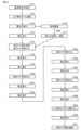
- FIG. 26 is a flowchart showing the process flow of the detection unit of the electric field sensor device 101 in the embodiment shown in FIG.
- Step S1 A voltage in a state where no person 201 is present is preset as a reference voltage. By storing the set reference voltage in the storage section, it is possible to eliminate the need to repeatedly set the reference voltage.
- Step S2 When the human detection operation starts, a change in voltage is determined.
- Step S3 If it is determined that there is no change in the voltage, it is determined that the person 201 is not present.
- Step S4 It is determined that the change in voltage is an increase.
- Step S5 If the change in voltage is an increase, it is determined that the person 201 is nearby. Further, the determination result is transmitted to the control side by the communication section.
- a threshold may be set for the change in voltage.
- the distance from the sensor to the person 201 may be determined based on the voltage value.
- the embodiment shown in FIG. 27 is another example of a human sensor using the electric field sensor device 104. That is, there is no noise source in the antenna element E1, and the antenna element E2 is grounded. When the person 201 approaches the antenna element E1, the antenna element E1 and the person 201 are coupled by capacitance. Therefore, as the person 201 approaches, the voltage increases. Furthermore, the distance to the person 201 can be determined from the voltage value.
- the electric field sensor device 102 is configured. In this electric field sensor device 102, when a person approaches the antenna element E1, noise energy is dispersed to the person, resulting in a voltage drop. Therefore, the approach of a person can be detected by detecting a voltage drop. Furthermore, the distance to a person can be determined from the voltage value.
- FIG. 28 shows an embodiment in which the present technology is applied to car detection.
- the vehicle 202 has a ground resistance Rx4 of 10 k ⁇ or more.
- An electric field sensor device 104 is constituted by an antenna element E1 (no noise source) and an antenna element E2 (earthed).
- Antenna element E1 is used as a sensor.
- the antenna element E1 and the car 202 are coupled by capacitance, the antenna size increases, and more energy of the electric field in the space is taken in. As the distance between the antenna element E1 and the vehicle 202 becomes shorter, the coupling becomes stronger. As a result, the voltage induced in the electric field sensor device 104 increases.
- the antenna element E1 which is the antenna to be coupled, can be made relatively large (all the metal parts of the device) in order to use a product metal part, such as a parking lot entrance gate or shutter gate, as an antenna. Compared to making an antenna, the size is larger and the capacity with respect to the approaching car 202 is also larger, which has the advantage of improving sensor sensitivity.
- FIG. 29 is a flowchart showing the processing flow of the detection unit of the electric field sensor device 104.
- Step S11 The voltage when the car 202 is not present is preset as the reference voltage. By storing the set reference voltage in the storage section, it is possible to eliminate the need to repeatedly set the reference voltage.
- Step S12 Then, when the vehicle detection operation starts, a change in voltage is determined.
- Step S13 If it is determined that there is no change in the voltage, it is determined that the car 202 is not present.
- Step S14 The change in voltage is determined to be an increase.
- Step S15 If the voltage change increases, it is determined that the car 202 is nearby. Further, the determination result is transmitted to the control side by the communication section. Based on this determination result, control such as opening a parking lot gate is performed, for example.
- a threshold value may be set for voltage changes.
- the distance to the car 202 may be determined based on the voltage value.
- the electric field sensor device 102 is configured. In this configuration, when the car 202 approaches the antenna element E1, noise energy is dispersed to the car 202, resulting in a voltage drop. Therefore, the approach of the car 202 can be detected by detecting a voltage drop. Furthermore, the distance to the car 202 can be determined from the voltage value.
- FIG. 30 schematically shows an example in which the electric field sensor device 101 is provided in conjunction with a lighting device, such as a fluorescent lamp device 211, installed in a room such as a conference room, a car, or the like.
- a lighting device such as a fluorescent lamp device 211
- an inverter is used to convert a commercial power source of 50 Hz or 60 Hz to direct current, and then to a high frequency signal of 20 to 50 kHz to turn on the fluorescent lamp.
- This lighting method eliminates the flickering characteristic of fluorescent lamps, compared to lighting using the frequency of a commercial power supply.
- a large amount of noise is generated from the commercial power supply due to switching and frequency conversion.
- the metal part of the fluorescent lamp device 211 By bringing the metal part of the fluorescent lamp device 211 into contact with the antenna element E1, it can be configured as an antenna element, and can be used as a sensor while harvesting energy and increasing the overall voltage. In this case, the configuration of the electric field sensor device 101 is suitable.
- Antenna element E2 is not grounded. Antenna element E2 is used as a sensor for person 201.
- the distance between the antenna element E2 and the person 201 becomes smaller, and the antenna element E2 and the person 201 are coupled with each other by capacitance, increasing the antenna size and making the energy of the electric field in the space more efficient. Take in a lot. As the distance between the antenna element E2 and the person becomes closer, the coupling becomes stronger. As a result, the voltage induced in the electric field sensor device 101 increases.
- FIG. 31 is a flowchart showing the process flow of the detection unit of the electric field sensor device 101.
- Step S21 The voltage when the person 201 is not present is preset as the reference voltage. By storing the set reference voltage in the storage section, it is possible to eliminate the need to repeatedly set the reference voltage.
- Step S22 Then, the person 201 approaches.
- Step S23 The voltage changes.
- Step S24 This change in voltage is determined to be an increase.
- Step S25 In this case, it is determined that the person 201 is in the room.
- Step S26 Further, the determination result is transmitted to the communication unit or directly to the control circuit of the fluorescent lamp device 211, and the fluorescent lamp device 211 is automatically turned on.
- Step S27 Also, the determination result is transmitted to the vacant room management system on the cloud by communication, and it is notified that the conference room is in use.
- a ground wire 213 and a power wire 214 are wired between the warm water bidet toilet seat 212 and the power outlet.
- the electric field sensor device 102 (including an electrode etc. as the antenna element E2) is inserted in the middle of the ground wire 213 of the warm water bidet toilet seat 212. Since there is a noise source in the warm-water-cleaning toilet seat 212, when a person approaches the warm-water-cleaning toilet seat 212, the voltage of the electric field sensor device 102 decreases, and the approach of the person can be detected.
- FIGS. 33A and 33B Another embodiment related to a warm water flush toilet seat will be described with reference to FIGS. 33A and 33B.
- a heater 215 and an aluminum foil (schematically shown as a ring-shaped portion) 216 are housed inside the resin toilet seat of the hot water bidet toilet seat, and the aluminum foil 216 is heated by the heater 215. This is done to warm the toilet seat.
- the aluminum foil 216 is in a floating state with respect to the ground.
- the electric field sensor device 103 is configured by using the aluminum foil 216 as the antenna element E2 and bringing the metal part of the warm water bidet toilet seat 212 into contact with the antenna element E1.
- the antenna element E2 and the person are coupled by capacitance, the antenna size increases, and more energy of the electric field in the space is taken in.
- the coupling becomes stronger.
- the voltage induced in the electric field sensor device 103 increases.
- FIG. 34 schematically shows yet another embodiment in which the present technology is applied to a warm water-washing toilet seat.
- a coil 217 is inserted between the ground wire 213 of the hot water bidet toilet seat and the ground in order to create a spatially floating state at frequencies that require the hot water bidet toilet seat, that is, to increase the impedance in the necessary frequency band. be done. Therefore, the circuit section 218 such as the power supply of the hot water bidet toilet seat 212 is in a state floating with respect to the ground.
- the electric field sensor device 101 is configured, and when a person approaches the toilet seat (antenna element E2), the voltage of the electric field sensor device 101 increases.
- a separation resistor Ry of 10 k ⁇ or more is inserted between the antenna elements E1 and E2 to separate the two antenna elements.
- Step S31 Setting a reference voltage. That is, the reference voltage is the voltage of the electric field sensor device 101 when the lights are off and no one is inside the toilet. By storing the set reference voltage in the storage section, it is possible to eliminate the need to repeatedly set the reference voltage.
- Step S32 It is determined from the voltage change whether a person approaches and opens the toilet door. When a person approaches and opens the door, the voltage of the electric field sensor device 101 increases relative to the reference voltage. Step S33: When it is determined that a person approaches and opens the toilet door, the determination result is transmitted to the lighting device, and the electric light inside the toilet is turned on.
- Step S34 It is determined whether a person has come directly in front of the toilet seat. When a person comes directly in front of the toilet seat, the voltage of the electric field sensor device 101 further increases. A further increase in this voltage is detected. The determination result is sent to the controller of the warm water flush toilet seat.
- Step S35 When it is determined that a person has come directly in front of the toilet seat, the control unit raises the cover of the toilet seat.
- Step S36 It is determined whether a person has sat on the toilet seat. From the further increase in the voltage of the electric field sensor device 101, it is detected that a person has sat on the toilet seat. When it is determined that a person has sat on the toilet seat, the determination result is transmitted to the controller of the warm water-cleaning toilet seat.
- Step S37 When it is determined in step S36 that a person has sat on the toilet seat, the determination result is sent to the control unit of the warm water-cleaning toilet seat, and the control unit turns on the deodorizing device and also masks the sound during defecation. A masking sound (for example, a babbling sound) is generated.
- a masking sound for example, a babbling sound
- Step S38 It is determined whether the person has left the toilet seat. It is detected from the voltage drop of the electric field sensor device 101 that the person has left the toilet seat. When it is determined that the person has left the toilet seat, the determination result is transmitted to the controller of the warm water-cleaning toilet seat. Step S39: When it is determined in step S38 that the person has left the toilet seat, water is flushed into the toilet bowl.
- Step S40 It is determined whether the person has left the toilet. A further drop in the voltage of the electric field sensor device 101 detects that a person has left the toilet. When it is determined that the person has exited the toilet, the determination result is sent to the controller of the warm water flush toilet seat.
- Step S41 When it is determined in step S40 that the person has left the toilet, the cover is lowered and closed. A predetermined time after the cover is closed, the deodorizer is turned off and the toilet light is turned off.
- the health condition may be determined by measuring this voltage every day. Also, by measuring voltage, it can be used like a body fat meter. Additionally, voltage changes due to the individual's unique walking style (method of approach) when entering the toilet are registered in advance, the individual is identified from the voltage change in the walking style, and data on the health condition is transmitted to the individual's smartphone, etc. You may also manage your health.
- an electric field sensor device such as a fluorescent lamp or light emitting diode
- a lighting device such as a fluorescent lamp or light emitting diode
- the metal part of the lighting device as an antenna
- the lighting of the lighting device can be controlled separately from the electric field sensor device attached to the warm water bidet toilet seat. You may also do so.
- FIG. 36 schematically shows the front surface of the ATM 221
- FIG. 37 schematically shows the side surface of the ATM 221.
- a metal frame 222 with an L-shaped cross section is provided to cover part of the front and top surfaces of the ATM 221.
- An ATM main body 223 is provided inside the ATM 221 .
- the ATM main body 223 includes a touch panel, a power supply circuit, a printer section, a banknote, a coin receiving and dispensing mechanism, and the like.
- a separation resistor Ry of 10 k ⁇ or more is connected between the metal frame 222 and the ATM main body 223.
- the metal frame 222 that comes into contact with the human body to be separated from the ATM main body 223, it is possible to prevent electric shocks and the like in the event of electrical leakage.
- the ATM main body 223 is grounded via a coil 224.
- the ATM main body 223 has a noise source, and the metal frame 222 does not have a noise source. In the frequency band of the noise source, the coil 224 causes the ATM main body 223 to be in a floating state with respect to the ground.
- a metal part within the ATM main body 223 is brought into contact with the antenna element E1.
- Metal frame 222 becomes antenna element E2. Therefore, when the electric field sensor device 101 is configured and a person approaches the ATM 221 (antenna element E2), the voltage of the electric field sensor device 101 increases. Further, when a person leaves the ATM 221, the voltage of the electric field sensor device 101 decreases. Note that the present technology can be applied to vending machines as well as ATMs.
- Step S51 Setting a reference voltage. That is, the voltage of the electric field sensor device 101 in a state where the lights installed near the ATM 221 are off and no one is present is set as the reference voltage. By storing the set reference voltage in the storage section, it is possible to eliminate the need to repeatedly set the reference voltage.
- Step S52 A person approaches the ATM 221.
- Step S53 It is determined from the voltage change whether a person has approached. When a person approaches, the voltage of the electric field sensor device 101 increases with respect to the reference voltage.
- Step S54 and Step S55 When it is determined that a person has approached, the camera installed in the ATM 221 is turned on and starts photographing the person, and the determination result is sent to the lighting device, and the lights are turned on. It will be lit.
- Step S56 Transaction using ATM 221 is started. Operations and processing such as inputting a password, fingerprint authentication, inserting an IC card, inputting an amount of money, and depositing/paying cash are performed. Changes in the voltage of the electric field sensor device 101 can be used for personal authentication.
- Step S57 The waveform of the voltage change when a person approaches the ATM 221 is confirmed. Since this waveform differs from person to person, it becomes a footsteps.
- a step pattern is a change in voltage that occurs when a conductor, a person, walks, and it becomes a unique waveform due to a person's spinal cord reflexes. By looking at this waveform, it is possible to identify an individual.
- Step S58 The footprint is analyzed, and the individual who approaches the ATM 221 is identified from the footprint and authenticated. If the authentication is successful, the start of the transaction is permitted. In this case, the establishment of authentication is comprehensively determined in conjunction with the results of other authentication means.
- Step S59 After the authentication is established, transactions such as input of amount, cash deposit/payment, and bankbook entry are performed, and the transaction is completed.
- Step S60 The person leaves the ATM 221, and the voltage of the electric field sensor device 101 drops to the reference voltage.
- Step S61 and Step S62 When it is determined that the person has left, the camera installed in the ATM 221 is turned off, the photographing of the person is completed, and the determination result is sent to the lighting device, and the lights are turned off. Ru.
- Figure 39 is an example of application to a car. Since a car is a conductor, the car is not limited to the object of detection, but can also be used as an antenna element for an electric field sensor device.
- the metal part 225 of the car frame, body, etc. (simply referred to as the car body) where the noise source exists is used as the antenna element E1
- the metal part 226 of the car door that is not grounded is used as the antenna element E1.
- An embodiment in which the electric field sensor device 101 is configured using the antenna element E2 is schematically shown.
- the antenna element E1 acquires electric field energy through capacitive coupling via the ground and space. Although this is still usable, the induced voltage level will be small.
- the car door 226 is connected to the car body 225 with noise sources at different potentials, and the car is divided into two antenna elements. It becomes possible to use only the car door 226 as a sensor. Note that since there are a plurality of car doors 226, each door may be set as a separate sensor. By using each door as a sensor, it is possible to identify which door a person approaches.
- the circuit section 229 of the electric field sensor device 101 is attached to a car door 226 via a conductor contact section 227, and connected to a car body 225 having a different potential from the car door via a cable 228. electrically connected.
- the circuit section 229 includes a rectifier circuit 2, a power storage section 3, a detection section 5, and a communication section 6.
- a separation resistor Ry of 10 k ⁇ or more may be inserted between the vehicle body 225 and the door 226.
- the circuit configuration in this case is as shown in FIG. 41, in which two input terminals of a rectifier circuit made up of diodes 61 to 64 are connected to both ends of a separation resistor Ry.
- the antenna element E2 of the electric field sensor device 101 operates as a human sensor. That is, when a person approaches the antenna element E2 (car door 226), the antenna element E2 and the person are coupled by capacitance, the antenna size increases, and more energy of the electric field in the space is taken in. Furthermore, as the distance between the antenna element E2 and the person becomes closer, the coupling becomes stronger. As a result, the voltage induced in the electric field sensor device 101 increases. Furthermore, because the antenna element E2 uses the car door 226 as an antenna, it can be made relatively large, so it is larger than if the antenna element is made from a separate member, and the capacitance with the approaching conductor is also larger. , which has the advantage of improving sensor sensitivity.
- FIG. 42 is a flowchart showing the process flow of the detection unit of the electric field sensor device 101.
- An example is the flow from when a person approaches the door of a car and gets into the car, until the person gets out of the car.
- Step S71 A voltage in a state where no person is near the car door 226 is preset as a reference voltage. By storing the set reference voltage in the storage section, it is possible to eliminate the need to repeatedly set the reference voltage.
- Step S72 A person approaches the car door 226.
- Step S73 A change in the voltage of the electric field sensor device 101 is detected. When a voltage increase is detected, it is determined that a person has approached.
- Step S74 If the approach of a person is detected, the detection result is sent to the car control unit, and the lights inside the car are turned on. Step S75: Furthermore, the car door is unlocked and the person opens the door. Step S76: The waveform of the voltage change when a person approaches the door 226 is confirmed. Since this waveform differs from person to person, it becomes a footsteps. Footprints are analyzed to identify and authenticate individuals who approach the vehicle. If the authentication is successful, the door can be unlocked in step S75.
- Step S78 A voltage change of the electric field sensor device 101 occurs.
- Step S79 A person gets into a car.
- Step S80 A person closes the car door 226.
- Step S81 A voltage change of the electric field sensor device 101 occurs. As the distance between the person and the car door 226 increases, the voltage decreases.
- Step S83 Open the car door 226 for the person to get out of the car.
- Step S84 A voltage change of the electric field sensor device 101 occurs. As the distance between the person and the car door 226 becomes narrower, the voltage increases.
- Step S85 When an increase in voltage is detected, the detection result is sent to the car control unit, and the lights inside the car are turned on.
- Step S86 The car door is closed.
- Step S87 A voltage change of the electric field sensor device 101 occurs. As the distance between the person and the car door 226 increases, the voltage decreases.
- Step S88 When the voltage drop is detected, the detection result is sent to the car control unit, and the lights inside the car are turned off.
- Step S89 The person leaves the car door 226.
- Step S90 A voltage change of the electric field sensor device 101 occurs. Since the distance between the person and the car door 226 further increases, the voltage further decreases to the reference voltage.
- Step S91 When it is detected that the voltage has reached the reference voltage, the detection result is transmitted to the car control unit, and the car door is locked.
- FIG. 43 schematically shows the area around the desk 231 in the office.
- the desk 231 is made of metal, and a conductive desk mat 232 is placed on the desk 231. Since the desk mat 232 is placed, the desk 231 can also be made of non-metallic material such as wood. Furthermore, a notebook PC 233 is placed on the desk 231. Note that this technology can be applied not only to desks but also to metal racks.
- the metal plate, electrode, meander antenna, etc. of the electric field sensor device 104 shown in FIG. 24 constitute an antenna element E2.
- Antenna element E2 is grounded to office ground via cable 235.
- the desk 231 is grounded via a grounding resistor Rx11
- the notebook PC 233 is grounded via a grounding resistor Rx12.
- a resistor Rx13 exists between the person 234 and the ground.
- the desk mat 232 functions as the antenna element E1 of the electric field sensor device 104.
- the desk 231 is made of metal, the desk 231 also functions as the antenna element E1.
- the desk 231 and desk mat 232 function as a sensor for the electric field sensor device 104.
- the notebook PC 233 when power is being supplied to the notebook PC 233, the notebook PC 233 becomes a noise source, and the electric field sensor device 102 is configured as shown in FIG. 44B.
- the electric field sensor device 102 when the person 234 approaches or touches the desk 231, noise is shunted to the person 234, so the voltage of the electric field sensor device 102 decreases.
- the reference voltage is set in advance in step S93.
- This reference voltage is set as the voltage of the electric field sensor device 104 when the office lights are off, there is no noise source such as the notebook PC 233, and no person 234 is near the desk 231.
- By storing the set reference voltage in the storage section it is possible to eliminate the need to repeatedly set the reference voltage.
- Step S94 A person approaches the desk 231, or power is supplied to the notebook PC 233.
- Step S95 A change in voltage (either rise or fall) is detected.
- Step S96 The detection result is transmitted to the light control device, and the light is turned on by the control device. Further, the detection result is transmitted to the control device of the air conditioner, and the control device turns on the air conditioner. Note that when a person leaves the desk 231 or stops supplying power to the notebook PC 233, the office lights are turned off and the air conditioner is turned off by detecting a voltage change.
- FIG. 46 shows an example of a drone.
- a main body part 242 is attached to the upper part of a metal body part 241, and a photographing device 244 is attached to a metal frame 243 at the lower part of the body part 241.
- the main body part 242 houses a control part, a battery part as a power source, etc. in a metal case.
- a circuit section of the electric field sensor device 101 is provided within this main body section 242.
- a plurality of support shafts are provided that extend substantially horizontally from the main body portion 242, and a motor 245 serving as a drive source for the rotary blade 246 is attached to the tip end surface of each support shaft.
- a rotary blade 246 is attached to the rotating shaft of the motor 245.
- a motor control circuit for controlling each motor is provided within the main body portion 242. The drone is remotely controlled by a controller on the ground.
- the drone By inserting a separation resistance Ry of 10 k ⁇ or more between the upper structure including the main body 242, motor 245, rotor 246, etc. and the lower structure including the metal frame 243, the drone is divided into the upper structure and the lower structure.
- the upper configuration is an antenna element E1 with a noise source
- the lower configuration is an antenna element E2 (without ground).
- Circuit parts such as the rectifier circuit 2 and the detection part 5 of the electric field sensor device 101 are housed within the main body part 242 .
- Antenna element E2 is used as a sensor.
- FIG. 47 An outline of the electric field sensor device 101 is shown in FIG. 47.
- the side surface 247 of the metal frame 243 is extended upward (or downward) to increase the antenna size, thereby improving the sensitivity of the side surface of the sensor.
- the electric field sensor device 101 can detect a high voltage line approaching the front of the drone in the direction of travel.
- the electric field sensor devices 101a and 101b may be provided by dividing the metal frame 243 into metal frames 243a (having a side surface 247a) and 243b (having a side surface 247b).
- One electric field sensor device 101a detects a high voltage line ahead in the direction of travel indicated by an arrow
- the other electric field sensor device 101b detects a high voltage line in the opposite direction to the direction of travel. In this way, by providing the electric field sensor devices 101a and 102b, it is possible to detect not only the presence or absence of a high voltage line, but also the direction in which the high voltage line exists.
- the drone has a photographing device 244, and if it photographs an obstacle during flight, it can be remotely controlled to avoid the obstacle. However, if conditions such as brightness are not good, the high voltage line may not be recognized as an obstacle. Since a leakage electric field exists around the high-voltage line, the electric field sensor device 101 (101a, 101b) can detect the proximity of the high-voltage line by detecting the leakage electric field, and based on that information, the high-voltage You can avoid touching the line.
- FIG. 49 is a flowchart for explaining the operation of the embodiment shown in FIG. 47 in which the present technology is applied to a drone.
- Step S101 A reference voltage is set. The voltage of the electric field sensor device 101 when the drone is in operation and there is no leakage electric field from the high voltage line is set as the reference voltage. By storing the set reference voltage in the storage section, it is possible to eliminate the need to repeatedly set the reference voltage.
- Step S102 The drone approaches the high voltage line.
- Step S103 A change in the voltage of the electric field sensor device 101 is determined. When a drone approaches a high-voltage line, a leakage electric field is detected and the voltage increases.
- Step S104 Approaching the high-voltage line is detected due to an increase in voltage, and the communication unit transmits to the remote controller the information that the vehicle is approaching the high-voltage line.
- Step S105 Display on the remote controller that the drone has approached the high voltage line. In this case, an alarm may be issued. This display allows the remote controller to be operated to prevent the drone from coming into contact with high-voltage lines.
- the transfer robot includes a metal frame 251 having wheels 252, a motor that drives the wheels 252, a power circuit, a control section, a communication section, etc. located on the top of the frame 251. It is composed of a housed metal main body part 253.
- the electric field sensor device 101 is configured such that the frame 251 serves as an antenna element E1, and the main body portion 253 serves as an antenna element E2.
- the antenna element E1 has a noise source such as a motor.
- a separation resistor Ry is inserted between the frame 251 and the main body portion 253.
- the front and rear end surfaces of the frame 251 in the direction of movement indicated by arrows are raised upward to improve the sensitivity of the sensor.
- the electric field sensor device 101 detects obstacles (persons, metal objects, etc.) in front of the transport robot in the direction of movement.
- electric field sensor devices 101a and 101b may be provided to detect the direction in which an obstacle exists.
- FIG. 52 is a flowchart for explaining the operation of an embodiment in which the present technology is applied to a transfer robot.
- Step S111 A reference voltage is set. The voltage of the electric field sensor device 101 when the transport robot is running and no obstacle is approaching is set as the reference voltage. By storing the set reference voltage in the storage section, it is possible to eliminate the need to repeatedly set the reference voltage.
- Step S112 The transport robot approaches an obstacle, such as a person.
- Step S113 A change in the voltage of the electric field sensor device 101 is determined. When a person approaches the transfer robot, the voltage increases.
- Step S114 The approach of a person is detected by the increase in voltage, and the transfer robot is stopped. The transfer robot is stopped and the voltage is reset to the reference voltage.
- Step S115 The transport operation of the transport robot is restarted. In this way, the transport robot is prevented from coming into contact with people.
- a potted plant 264 such as a foliage plant is used as the antenna element E2
- a potted plant 264 is placed at the reception desk of a company.
- a power adapter 262 is used to charge the notebook PC 261, and the power adapter 262 is connected to a commercial power outlet 263.
- notebook PC 261 is set as antenna element E1 having a noise source.
- the potted plant 264 has sap, which is an electrolytic solution, and can be used as a conductor (antenna element).
- the roots of the potted plant 264 are connected to the soil (earth) via an equivalent resistance 265 corresponding to the amount of water in the soil. Therefore, as shown in FIG. 54, an electric field sensor device 101 is configured.
- the circuit section 266 of the electric field sensor device 101 is connected to the notebook PC 261 and the potted plant 264.
- Circuit section 266 includes rectifier circuit 2 , power storage section 3 , detection section 5 , and communication section 6 .
- a notebook PC 261, which is the antenna element E1, or a potted plant 264, which is the antenna element E2, is used as a sensor.
- the equivalent resistance 265 decreases when water is replenished, the coupling with the ground increases, and the voltage of the electric field sensor device 101 increases.
- FIG. 55 is a flowchart for explaining the operation when the potted plant 264 is used as a human sensor in the embodiment shown in FIGS. 53 and 54.
- Step S111 A person approaches the potted plant 264.
- Step S112 A change in the voltage of the electric field sensor device 101 is detected.
- the voltage value of the electric field sensor device 101 when no one is present differs depending on the equivalent resistance 265 of the potted plant 264.
- the potted plant 264 has a high moisture content, the value of the equivalent resistance 265 is relatively small, and the voltage in the absence of people is relatively large.
- the value of the equivalent resistance 265 is relatively large, and the voltage when no one is present is relatively small. In either case, when a person approaches, the voltage of the electric field sensor device 101 increases.
- Step S113 If it is determined that the voltage change detected in step S112 is an increase, it is recognized that a person has approached (is at the reception desk).
- Step S114 The recognition result is transmitted to the reception system, and the arrival of the person is notified. For example, a chime sounds.
- Step S115 The recognition result is transmitted to the reception system, and photographing by a photographing device installed near the reception starts.
- the notebook PC 261 (antenna element E1) side may be used as a sensor.
- noise from the noise source is shunted to the person, and the voltage of the electric field sensor device 101 changes in a decreasing direction. By detecting this voltage change, it is recognized that a person has come to the reception desk.
- FIG. 53 can be applied to a system for managing the water supply period for potted plants 264.
- the flow of processing in that case is shown in the flowchart of FIG. Step S121:
- a reference voltage is set.
- the voltage of the electric field sensor device 101 when the moisture supplied to the potted plant 264 is appropriate is set as the reference voltage.
- By storing the set reference voltage in the storage section it is possible to eliminate the need to repeatedly set the reference voltage.
- Step S122 The potted plant 264 becomes dry and lacks moisture.
- Step S123 Since the equivalent resistance 265 increases, the connection with the ground becomes weaker, and the voltage of the electric field sensor device 101 decreases.
- Step S124 When the voltage drops below a predetermined value, the person in charge of water replenishment is notified that there is no water.
- Step S125 Upon receiving this notification, water is supplied. Note that the water supply is not limited to a manual method, but an automatic method using a water supply device is also possible.
- Step S126 The equivalent resistance 265 decreases due to water supply, and the voltage of the electric field sensor device 101 increases. Then, when the potted plant 264 dries over time, the process returns to step S122.
- FIG. 57 shows an electric field sensor device 101 in which a tree 271 planted on the ground is used as an antenna element E2.
- a cable 272 is connected to the tree 271, and the antenna element E1 and the tree 271 (antenna element E2) constitute an antenna device.
- a signal generator 273 is provided as a noise source for antenna element E1.
- the circuit section 274 of the electric field sensor device 101 is connected to the signal generator 273 and the tree 271.
- the circuit section 274 includes a rectifier circuit 2, a power storage section 3, a detection section 5, and a communication section 6.
- the ground resistance of the tree 271 changes depending on the amount of moisture in the soil, and the degree of coupling between the earth and the tree 271 (antenna element E2) changes.
- the amount of water is large, the ground resistance becomes small, the coupling of the antenna element E2 with the ground becomes strong, and the voltage of the electric field sensor device 101 becomes large.
- the amount of water is small, the ground resistance becomes large, the coupling of the antenna element E2 with the ground becomes weak, and the voltage of the electric field sensor device 101 becomes small. In this way, the amount of water in the ground can be detected from the voltage of the electric field sensor device 101.
- Power for the electric field sensor device 101 and the signal generator 273 is supplied from, for example, a solar cell (not shown).
- the moisture content monitoring system receives data on the moisture content of a place where a plurality of trees are planted, and predicts the risk of a disaster such as a landslide. It is also possible to detect growth or disease in a tree based on changes in the electrolyte in the tree. Furthermore, as explained with reference to FIG. 53, it is also possible to supply irrigation water, fertilizer, etc. as appropriate when the amount of water is insufficient.
- the antenna element E2 when a 2V rectangular wave is applied to the antenna element E1 at a frequency of 1 kHz from the signal generator 273 as a noise source connected to the antenna element E1, the antenna element E2 connected to the plant is applied. A signal corresponding to the frequency and voltage applied to the antenna element E1 is induced as an image. In this way, the antenna element E2 induces electric power corresponding to the signal input to the antenna element, so by appropriately selecting the frequency and electric energy, it can be expected to have an insect repellent effect that keeps pests away from the plant. .
- the electrical stimulation induced in plants causes moderate stress on plants, and can be expected to have the effect of increasing sugar content in vegetables such as tomatoes and fruits such as grapes. It can also be used by connecting the GND of the signal generator 273 to the same soil as the plants.
- FIG. 58 is an exploded perspective view for explaining an embodiment in which the present technology is applied to a sensor that is provided in a mobile electronic device, such as wireless headphones, and detects hand movements.
- the synthetic resin housing of the wireless headphones is not a conductor, so the wireless headphones are insulated from people.
- a main board 281, a lithium ion secondary battery 282, and a speaker driver 283 are housed inside the housing.
- An electrode within main board 281 is used as antenna element E1.
- the antenna element E1 Since noise is generated within the main board 281 due to signal processing, the antenna element E1 has a noise source. Further, an electrode 284 is attached to the housing, and the electrode 284 is used as the antenna element E2. Antenna element E2 is not grounded. Therefore, the electric field sensor device 101 is configured by the antenna element E1 and the antenna element E2. Antenna element E2 is used as a sensor for hand 285.
- the circuit section 286 of the electric field sensor device 101 is connected to the electrodes within the main board 281 and the electrodes 284 . Circuit section 286 includes rectifier circuit 2 , power storage section 3 , detection section 5 , and communication section 6 .
- the electric field sensor device 101 can detect when a hand 285 of a person wearing headphones approaches the electrode 284. Therefore, since the voltage of the electric field sensor device 101 changes when the hand 285 approaches, the operation of the headphones can be controlled based on this voltage change. Furthermore, by providing a plurality of electric field sensor devices, it becomes possible to detect the direction in which the hand 285 approaches, and more types of control can be performed.
- a reference voltage is set.
- the voltage of the electric field sensor device 101 when the headphones are worn on the ears and the hand 285 is not near the headphones is set as the reference voltage.
- Step S132 Hand 285 approaches the headphones (electrode 284).
- Step S133 The electrode 284 and the hand 285 are spatially coupled, the electric field energy taken in increases, and the voltage of the electric field sensor device 101 increases.
- Step S134 When the voltage of the electric field sensor device 101 rises above the reference voltage, it is detected that the hand 285 approaches. The detection result is transmitted to the headphone control unit.
- Step S135 Based on the detection of the hand 285, the control unit controls the playback operation of the headphones. For example, by providing a plurality of electrodes 284, the movement of the hand can be detected, that is, the playback start, playback stop, fast forwarding, etc. of a song can be controlled.
- the metal part of the product as an antenna, it is possible to capture more of the quasi-electrostatic field and radio wave energy generated in space. Furthermore, it is possible to convert power and noise leaking from power cords and inverters into energy. If the captured energy is rectified and stored in a power storage element such as a secondary battery, it can be used as a power source for an electric field sensor device, so energy can be used efficiently. Therefore, it can be related to Goal 7 "Affordable and Clean Energy" of the SDGs (Sustainable Development Goals) adopted at the United Nations Summit in 2015.
- the present technology is not limited to the embodiments described above, and various modifications based on the technical idea of the present technology are possible.
- one or more arbitrarily selected modes of deformation can be combined as appropriate.
- the configurations, methods, processes, shapes, materials, numerical values, etc. of the above-described embodiments can be combined with each other without departing from the gist of the present technology.
- energy may be stored by using the present technology in conjunction with power generation using natural energy, such as solar power generation, or thermoelectric conversion elements.
- An antenna device having a dipole structure that receives an electric field and has a first antenna element connected to or in contact with a conductor that has a certain resistance value with the ground, and a second antenna element that is grounded or not grounded. and, a rectifier circuit that rectifies a signal induced in the antenna device; and a detection unit that detects the level of the output voltage of the rectifier circuit, The detection unit detects a change in the level of the output voltage caused by spatial coupling or contact of the first antenna element or the second antenna element that is not grounded with another conductor different from the conductor.
- An electric field sensor device that detects the state or situation of the other conductor.
- the electric field sensor device (2) The electric field sensor device according to (1), wherein a noise source is present in the first antenna element. (3) The electric field sensor device according to (1) or (2), wherein a resistor having a resistance value of 10 k ⁇ or more is present between the conductor and the ground. (4) The conductor is divided into at least a first and second conductor with a resistance of 10 k ⁇ or more, and the divided first and second conductors constitute the first antenna element and the second antenna element. The electric field sensor device according to any one of (1) to (3). (5) The electric field sensor device according to any one of (1) to (4), wherein the rectifier circuit is a half-wave or full-wave rectifier circuit.
- the electric field sensor device wherein the rectifying diode used in the rectifying circuit is made of silicon, which has a small leakage current when a back electromotive force is generated.
- the other conductor is any one of a personal computer, a car, a high-voltage line, a human body, and a living creature (animals and plants other than humans).
- the electric field sensor device further comprising a power storage unit charged with electric power output from the rectifier circuit.
- the electric field sensor device further comprising communication means for transmitting information obtained from the detection section to another device.
- the electric field sensor device wherein the first antenna element is connected to the ground via a cable.
- the first antenna element is constituted by a metal conductor such as an electric refrigerator, a vending machine, an ATM, a transportation robot, a metal desk, or a metal rack.
- the first antenna element is a conductor with a noise source
- the second antenna element is an ungrounded potted plant
- the first antenna element is a conductor with a noise source
- the second antenna element is a tree planted in the soil
- the electric field sensor device according to (1) wherein the change in the amount of water is detected by a change in the level of the output voltage caused by a change in the amount of water contained in the soil.
- the first antenna element is a conductor with a signal generator
- the second antenna element is a plant planted in soil
- the electric field sensor device according to (1) wherein the signal generated by the signal generator is induced in the plant.
- the first antenna element is a conductor having a noise source
- the second antenna element is an electrode provided on an electronic device, detecting that a part of the human body approaches the electrode by a change in the level of the output voltage;
- the electric field sensor device according to (1) wherein the operation of the electronic device is controlled based on detection.
Landscapes
- Physics & Mathematics (AREA)
- General Physics & Mathematics (AREA)
- Engineering & Computer Science (AREA)
- Electromagnetism (AREA)
- Remote Sensing (AREA)
- Life Sciences & Earth Sciences (AREA)
- Power Engineering (AREA)
- Environmental & Geological Engineering (AREA)
- General Life Sciences & Earth Sciences (AREA)
- Geophysics (AREA)
- Geology (AREA)
- Computer Networks & Wireless Communication (AREA)
- Details Of Aerials (AREA)
- Geophysics And Detection Of Objects (AREA)
- Variable-Direction Aerials And Aerial Arrays (AREA)
Abstract
Description
アンテナ装置に誘起される信号を整流する整流回路と、
整流回路の出力電圧のレベルを検出する検出部とを備え、
検出部は、第1のアンテナエレメント又はアースされない第2のアンテナエレメントが、導体とは異なる別の導体と空間的に結合又は接触することによって生じる出力電圧のレベルの変化を検出して別の導体の状態や状況を検知する電界センサー装置である。
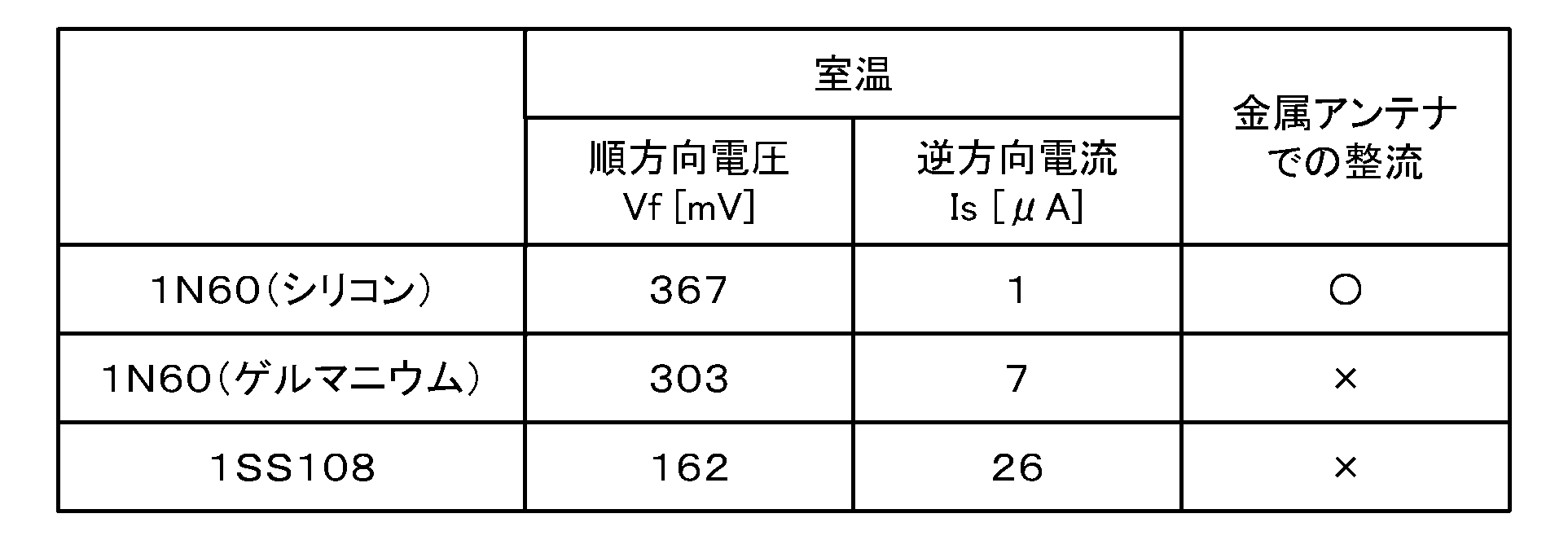
D接地では、直流抵抗が、100Ω以下となる接地抵抗が求められる。なお、低圧電路において、地絡(漏電)を生じた場合に0.5秒以内に電路を自動的に遮断する装置を設けている場合には、直流抵抗が、500Ω以下となる接地抵抗を用いてもよい。例えば、暗電流を検知した場合に機器に供給する電力を遮断する仕組みがあれば、D接地において100Ωから500Ωへの接地抵抗の変更が認められる。
これまで、機器110を収穫する周波数に合わせて、浮いた状態にするフィルタについて、説明したが、アースの途中にあるフィルタのハイパスフィルタ121の出力端子(オープン)にハーベスタ4の第1のアンテナエレメントを接続して、第2のアンテナエレメントは、アースまたは、基板上の銅箔のメアンダライン等アンテナで構成することも可能である。例えば、工場にあるGNDラインがある3端子のコンセントの場合、機器110のコンセントと接続する部分に構成することが出来るので、機器110ごとに簡単に構成でき、それぞれの機器110の状態の管理等を行うことも可能となる。
電界センサー装置101(図10、図24A)においては、導体である機器の金属部と接触または、接続されないアンテナエレメントE2が、アースされていないので、アンテナエレメントE2側に、人201や大きな金属等の導体が近づいた場合に、アンテナエレメントE2側の機器の金属部と人201や金属等の導体が空間的に結合する。その結果、アンテナサイズが大きくなり、空間にある電界のエネルギーをより多く取り込めることになる。この場合は、電界センサー装置101に誘起される電圧が上昇することになり、電圧の上昇を見ることで、アンテナエレメントE2側がセンサーとして機能する。
図25に示す実施形態は、電界センサー装置101による人センサーである。アンテナエレメントE2は、グランドとの間に接地抵抗Rx2を有する。接地抵抗Rx2は、上述したように、10kΩ以上の値を有しており、ハーベスタから十分な出力を得ることが可能とされている。
ステップS1:人201がいない状態の電圧が基準電圧として予め設定される。設定された基準電圧を記憶部に記憶しておくことによって、基準電圧の設定を繰り返すことを不要とすることができる。
ステップS2:人検出動作になると、電圧の変化が判定される。
ステップS4:電圧の変化が上昇であると判定される。
ステップS5:電圧の変化が上昇の場合には、人201が近くにいると判定される。さらに、判定結果は、通信部によって制御側に送信される。電圧の変化にしきい値を設定してもよい。さらに、電圧の値によってセンサーから人201までの距離を判定するようにしてもよい。
ステップS11:車202がない状態の電圧が基準電圧として予め設定される。設定された基準電圧を記憶部に記憶しておくことによって、基準電圧の設定を繰り返すことを不要とすることができる。
ステップS12:そして、車検出動作になると、電圧の変化が判定される。
ステップS14:電圧の変化が上昇と判定される。
ステップS15:電圧変化が上昇の場合には、車202が近くにあると判定される。さらに、判定結果は、通信部によって制御側に送信される。この判定結果によって例えば駐車場のゲートが開かれるような制御がなされる。電圧の変化に対するしきい値を設定してもよい。さらに、電圧の値によって車202までの距離を判定するようにしてもよい。
ステップS21:人201がいない時の電圧が基準電圧として予め設定される。設定された基準電圧を記憶部に記憶しておくことによって、基準電圧の設定を繰り返すことを不要とすることができる。
ステップS22:そして、人201が接近する。
ステップS23:電圧が変化する。
ステップS25:この場合には、人201が部屋内にいると判定される。
ステップS26:さらに、判定結果は、通信部又は直接的に蛍光灯装置211の制御回路に伝送され、蛍光灯装置211が自動的に点灯される。
ステップS27:また、判定結果が通信によってクラウド上の空き室管理システムに対して伝送され、当該会議室が使用中であることが知らされる。
ステップS31:基準電圧を設定する。すなわち、トイレ内で電灯が消灯しており、且つ人がいない状態の電界センサー装置101の電圧を基準電圧とする。設定された基準電圧を記憶部に記憶しておくことによって、基準電圧の設定を繰り返すことを不要とすることができる。
ステップS33:人が接近し、トイレのドアを開けたと判定されると、判定結果が照明装置に対して送信され、トイレ内の電灯が点灯される。
ステップS35:人が便座の直前に来たと判定されると、制御部によって便座のカバーがアップされる。
ステップS36:人が便座に座ったかどうかが判定される。電界センサー装置101の電圧のさらなる上昇から人が便座に座ったことが検出される。人が便座に座ったと判定されると、判定結果が温水洗浄便座の制御部に送信される。
ステップS39:ステップS38において、人が便座から離れたと判定されると、便器内に水を流す。
ステップS41:ステップS40において人がトイレから出たと判定されると、カバーが降りて閉じる。カバーが閉じてから所定時間後に消臭がOFFし、トイレの電灯が消灯する。
ステップS51:基準電圧を設定する。すなわち、ATM221の付近に設置されている電灯が消灯しており、且つ人がいない状態の電界センサー装置101の電圧を基準電圧として設定する。設定された基準電圧を記憶部に記憶しておくことによって、基準電圧の設定を繰り返すことを不要とすることができる。
ステップS53:人が接近したかどうかが電圧変化から判定される。人が接近することによって電界センサー装置101の電圧が基準電圧に対して上昇する。
ステップS54及びステップS55:人が接近したと判定されると、ATM221に設けられているカメラがONとされ、人の撮影が開始されると共に、照明装置に対して判定結果が送信され、電灯が点灯される。
ステップS57:人がATM221に接近する時の電圧の変化の波形が確認される。この波形は、人毎に相違しているので、歩紋となる。歩紋とは、導体である人が歩くときに発生する電圧の変化であり、人の脊髄反射により固有の波形となる。この波形を見ることで、個人を特定することが可能となる。
ステップS58:歩紋が解析され、歩紋からATM221に接近してきた個人を特定し、認証を行う。認証が成立する場合に、取引の開始が許可される。この場合、他の認証手段の結果と合わせて総合的に認証の成立を判断するようになされる。
ステップS60:人がATM221から離れ、電界センサー装置101の電圧が基準電圧に下降する。
ステップS61及びステップS62:人が離れたと判定されると、ATM221に設けられているカメラがOFFとされ、人の撮影が終了すると共に、照明装置に対して判定結果が送信され、電灯が消灯される。
ステップS71:人が車のドア226の近くにいない状態の電圧が基準電圧として予め設定される。設定された基準電圧を記憶部に記憶しておくことによって、基準電圧の設定を繰り返すことを不要とすることができる。
ステップS72:人が車のドア226に接近する。
ステップS73:電界センサー装置101の電圧の変化が検出される。電圧の上昇が検出されると、人が接近したと判定される。
ステップS75:さらに、車のドア鍵が解除され、人がドアを開ける。
ステップS76:人がドア226に接近する時の電圧の変化の波形が確認される。この波形は、人毎に相違しているので、歩紋となる。歩紋が解析され、歩紋から接近してきた個人を特定し、認証を行う。認証が成立する場合に、ステップS75においてドアの鍵の解除が可能とされる。
ステップS79:人が車に乗る。
ステップS80:人が車のドア226を閉める。
ステップS81:電界センサー装置101の電圧変化が生じる。人と車のドア226の間隔が拡がるので、電圧が低下する。
ステップS82:電圧の低下が検出されると、人が乗車したと判定される。判定結果が車の制御部に対して送信され、車内のライトが消灯される。
ステップS84:電界センサー装置101の電圧変化が生じる。人と車のドア226の間隔が狭くなるので、電圧が上昇する。
ステップS85:電圧の上昇が検出されると、検出結果が車の制御部に対して送信され、車内のライトが点灯される。
ステップS87:電界センサー装置101の電圧変化が生じる。人と車のドア226の間隔が拡がるので、電圧が下降する。
ステップS88:電圧の下降が検出されると、検出結果が車の制御部に対して送信され、車内のライトが消灯される。
ステップS90:電界センサー装置101の電圧変化が生じる。人と車のドア226の間隔がさらに拡がるので、電圧がさらに下降して基準電圧となる。
ステップS91:基準電圧となったことが検出されると、検出結果が車の制御部に対して送信され、車のドア鍵が施錠される。
ステップS95:電圧の変化(上昇及び下降のいずれか)が検出される。
ステップS96:検出結果が電灯の制御装置に対して送信され、制御装置によって電灯が点灯される。また、検出結果が空調機器の制御装置に対して送信され、制御装置によって空調機器がONされる。なお、人が机231から離れたり、ノートPC233に対する電源の供給を停止したりした場合には、電圧の変化の検出によって、オフィスの電灯が消灯され、また、空調機器がOFFされる。
ステップS101:基準電圧が設定される。ドローンが動作中で、高圧線の洩れ電界がない状態での電界センサー装置101の電圧を基準電圧に設定する。設定された基準電圧を記憶部に記憶しておくことによって、基準電圧の設定を繰り返すことを不要とすることができる。
ステップS103:電界センサー装置101の電圧の変化が判定される。ドローンが高圧線に接近した場合、漏れ電界が検知され、電圧が上昇する。
ステップS104:電圧の上昇によって高圧線に接近したことが検出され、高圧線に接近したことが通信部によってリモートコントローラに対して送信される。
ステップS105:リモートコントローラにおいて、ドローンが高圧線に接近したことを表示する。この場合、警報を発生してもよい。この表示を見てリモートコントローラが操作され、ドローンが高圧線に接触することを防止できる。
ステップS111:基準電圧が設定される。搬送ロボットが走行状態で、障害物が接近していない状態での電界センサー装置101の電圧を基準電圧に設定する。設定された基準電圧を記憶部に記憶しておくことによって、基準電圧の設定を繰り返すことを不要とすることができる。
ステップS113:電界センサー装置101の電圧の変化が判定される。搬送ロボットに人が接近した場合、電圧が上昇する。
ステップS114:電圧の上昇によって人が接近したことが検出され、搬送ロボットが停止される。搬送ロボットが停止されると共に、電圧が基準電圧にリセットされる。
ステップS115:搬送ロボットの搬送動作が再開される。このようにして、搬送ロボットが人に接触することが回避される。
ステップS111:鉢植え植物264に対して人が接近する。
ステップS112:電界センサー装置101の電圧の変化が検出される。人がいない場合の電界センサー装置101の電圧の値は、鉢植え植物264の等価抵抗265によって相違する。鉢植え植物264の水分が多いと、等価抵抗265の値が比較的小さく、人がいない状態の電圧が比較的大きい。一方、水分が少ないと、等価抵抗265の値が比較的大きく、人がいない状態の電圧が比較的小さい。何れの場合でも、人が接近すると、電界センサー装置101の電圧が上昇する。
ステップS114:認識結果が受付システムに伝送され、人が来たことが報知される。例えばチャイムが鳴らされる。
ステップS115:認識結果が受付システムに伝送され、受付付近に設置されている撮影装置による撮影が開始される。
ステップS121:基準電圧が設定される。鉢植え植物264に供給されている水分が適切な場合の電界センサー装置101の電圧を基準電圧に設定する。設定された基準電圧を記憶部に記憶しておくことによって、基準電圧の設定を繰り返すことを不要とすることができる。
ステップS123:等価抵抗265が大きくなるので、大地との結合が弱まり、電界センサー装置101の電圧が低下する。
ステップS124:電圧の所定値より低下すると、水がないことを水補給係の人に連絡する。
ステップS125:この連絡を受けて給水が行われる。なお、給水は、人的な方法に限らず、給水装置による自動的な方法も可能である。
ステップS126:給水によって等価抵抗265が小さくなり、電界センサー装置101の電圧が上昇する。そして、時間が経過して鉢植え植物264が乾燥すると、処理がステップS122に戻る。
また、植物に誘起される電気的な刺激は、植物への適度なストレスとなり、トマト等の野菜や葡萄等の果物に対して、糖度を増す効果も期待出来る。前記信号発生器273のGNDを植物と同じ土壌に接続しても使用可能である。
ステップS131:基準電圧が設定される。ヘッドホンを耳に装着し、且つ、手285がヘッドホンの近くに存在しない時の電界センサー装置101の電圧を基準電圧に設定する。設定された基準電圧を記憶部に記憶しておくことによって、基準電圧の設定を繰り返すことを不要とすることができる。
ステップS133:電極284と手285が空間的に結合し、取り込まれる電界エネルギーが増加し、電界センサー装置101の電圧が上昇する。
ステップS134:基準電圧より電界センサー装置101の電圧が上昇したことにより、手285が接近したことが検出される。検出結果がヘッドホンの制御部に対して送信される。
ステップS135:手285が検出されたことに基づいて制御部がヘッドホンの再生動作を制御する。例えば、電極284を複数個設けることで、手の動きが検知できるので、すなわち、曲の再生開始、再生停止、早送り等の制御がなされる。
(1)
グランドと一定の抵抗値をもって存在する導体と接続又は接触される第1のアンテナエレメントと、グランドとアースされるか、又はアースされない第2のアンテナエレメントを有する、電界を受信するダイポール構造のアンテナ装置と、
前記アンテナ装置に誘起される信号を整流する整流回路と、
前記整流回路の出力電圧のレベルを検出する検出部とを備え、
前記検出部は、前記第1のアンテナエレメント又はアースされない前記第2のアンテナエレメントが、前記導体とは異なる別の導体と空間的に結合又は接触することによって生じる前記出力電圧のレベルの変化を検出して前記別の導体の状態や状況を検知する電界センサー装置。
(2)
前記第1のアンテナエレメントにノイズ源が存在する(1)に記載の電界センサー装置。
(3)
前記導体とグランドの間に抵抗値が10kΩ以上の抵抗が存在する(1)又は(2)に記載の電界センサー装置。
(4)
前記導体を10kΩ以上の抵抗で、少なくとも第1および第2の導体に分割して、分割された前記第1および第2の導体によって前記第1のアンテナエレメント及び第2のアンテナエレメントを構成するようにした(1)から(3)のいずれかに記載の電界センサー装置。
(5)
前記整流回路が、半波、又は全波整流回路である(1)から(4)のいずれかに記載の電界センサー装置。
(6)
前記整流回路に用いられる整流用のダイオードは、逆起電力時の漏れ電流が少ないシリコンで作られた(5)に記載の電界センサー装置。
(7)
前記別の導体が、パソコン、車、高圧線、人体、生物(人以外の動物及び植物)のいずれかである(1)に記載の電界センサー装置。
(8)
前記整流回路から出力された電力が充電される蓄電部が設けられた(1)に記載の電界センサー装置。
(9)
前記検出部から得た情報を他の機器に送信するための通信手段を有する(1)記載の電界センサー装置。
(10)
前記(1)記載の第1のアンテナエレメントであって、前記第1のアンテナエレメントはケーブルを介してグランドに接続されている(1)記載の電界センサー装置。
(11)
前記第1のアンテナエレメントが、電気冷蔵庫、自動販売機、ATM、搬送ロボット、金属机、金属ラック等の金属導体によって構成された(1)記載の電界センサー装置。
(12)
前記第1のアンテナエレメントがノイズ源を有する導体であり、前記第2のアンテナエレメントがアースされない鉢植え植物であり、
前記鉢植え植物と人が空間的に結合又は接触することによって生じる前記出力電圧のレベルの変化によって、前記鉢植え植物に対して人体が接近したことを検知するようにした(1)に記載の電界センサー装置。
(13)
前記第1のアンテナエレメントがノイズ源を有する導体であり、前記第2のアンテナエレメントが土に植えられている木であり、
前記土に含まれる水分量の変化により生じる前記出力電圧のレベルの変化によって、前記水分量の変化を検知するようにした(1)に記載の電界センサー装置。
(14)
前記第1のアンテナエレメントが信号発生器を有する導体であり、前記第2のアンテナエレメントが土に植えられている植物であり、
前記信号発生器による信号を前記植物に誘起させるようにした(1)に記載の電界センサー装置。
(15)
前記第1のアンテナエレメントがノイズ源を有する導体であり、前記第2のアンテナエレメントが電子機器に設けられた電極であり、
前記出力電圧のレベルの変化によって、前記電極に対して人体の一部が接近することを検知し、
検知に基づいて前記電子機器の動作を制御するようにした(1)に記載の電界センサー装置。
符号の説明
4・・・ハーベスタ、5・・・検出部、6,7・・・通信部
8・・・制御部、11・・・導電部材、15・・・給電点
19・・・グランド電極
20A,20B、20C・・・アンテナエレメント
101,102,103,104・・・電界センサー装置
105・・・電気冷蔵庫、201・・・人、202・・・車
211・・・蛍光灯装置、212・・・温水洗浄便座
221・・・ATM、225・・・車本体、226車のドア
231・・・机、233・・・ノートPC、242・・・ドローンの本体部
243・・・ドローンの金属フレーム
251・・・搬送ロボットのフレーム
253・・・搬送ロボットの本体部
264・・・鉢植え植物、271・・・木
Claims (15)
- グランドと一定の抵抗値をもって存在する導体と接続又は接触される第1のアンテナエレメントと、グランドとアースされるか、又はアースされない第2のアンテナエレメントを有する、電界を受信するダイポール構造のアンテナ装置と、
前記アンテナ装置に誘起される信号を整流する整流回路と、
前記整流回路の出力電圧のレベルを検出する検出部とを備え、
前記検出部は、前記第1のアンテナエレメント又はアースされない前記第2のアンテナエレメントが、前記導体とは異なる別の導体と空間的に結合又は接触することによって生じる前記出力電圧のレベルの変化を検出して前記別の導体の状態や状況を検知する電界センサー装置。 - 前記第1のアンテナエレメントにノイズ源が存在する請求項1に記載の電界センサー装置。
- 前記導体とグランドの間に抵抗値が10kΩ以上の抵抗が存在する請求項1に記載の電界センサー装置。
- 前記導体を10kΩ以上の抵抗で、少なくとも第1および第2の導体に分割して、分割された前記第1および第2の導体によって前記第1のアンテナエレメント及び第2のアンテナエレメントを構成するようにした請求項1に記載の電界センサー装置。
- 前記整流回路が、半波、又は全波整流回路である請求項1に記載の電界センサー装置。
- 前記整流回路に用いられる整流用のダイオードは、逆起電力時の漏れ電流が少ないシリコンで作られた請求項5に記載の電界センサー装置。
- 前記別の導体が、パソコン、車、高圧線、人体、生物(人以外の動物及び植物)のいずれかである請求項1に記載の電界センサー装置。
- 前記整流回路から出力された電力が充電される蓄電部が設けられた請求項1に記載の電界センサー装置。
- 前記検出部から得た情報を他の機器に送信するための通信手段を有する請求項1記載の電界センサー装置。
- 前記請求項1記載の第1のアンテナエレメントであって、前記第1のアンテナエレメントはケーブルを介してグランドに接続されている請求項1記載の電界センサー装置。
- 前記第1のアンテナエレメントが、電気冷蔵庫、自動販売機、ATM、搬送ロボット、金属机、金属ラック等の導体によって構成された請求項1記載の電界センサー装置。
- 前記第1のアンテナエレメントがノイズ源を有する導体であり、前記第2のアンテナエレメントがアースされない植物であり、
前記植物と人が空間的に結合又は接触することによって生じる前記出力電圧のレベルの変化によって、前記植物に対して人体が接近したことを検知するようにした請求項1に記載の電界センサー装置。 - 前記第1のアンテナエレメントがノイズ源を有する導体であり、前記第2のアンテナエレメントが土に植えられている植物であり、
前記植物に含まれる水分量の変化により生じる前記出力電圧のレベルの変化によって、前記水分量の変化を検知するようにした請求項1に記載の電界センサー装置。 - 前記第1のアンテナエレメントが信号発生器を有する導体であり、前記第2のアンテナエレメントが土に植えられている植物であり、
前記信号発生器による信号を前記植物に誘起させるようにした請求項1に記載の電界センサー装置。 - 前記第1のアンテナエレメントがノイズ源を有する導体であり、前記第2のアンテナエレメントが電子機器に設けられた電極であり、
前記出力電圧のレベルの変化によって、前記電極に対して人体の一部が接近又は接触することを検知し、
前記検知に基づいて前記電子機器の動作を制御するようにした請求項1に記載の電界センサー装置。
Priority Applications (4)
| Application Number | Priority Date | Filing Date | Title |
|---|---|---|---|
| CN202380048949.6A CN119487423A (zh) | 2022-06-29 | 2023-06-19 | 电场传感器装置 |
| EP23831177.3A EP4550007A4 (en) | 2022-06-29 | 2023-06-19 | ELECTRIC FIELD DETECTION DEVICE |
| JP2024530709A JPWO2024004731A1 (ja) | 2022-06-29 | 2023-06-19 | |
| KR1020257001472A KR20250029129A (ko) | 2022-06-29 | 2023-06-19 | 전계 센서 장치 |
Applications Claiming Priority (4)
| Application Number | Priority Date | Filing Date | Title |
|---|---|---|---|
| JP2022104134 | 2022-06-29 | ||
| JP2022-104134 | 2022-06-29 | ||
| JP2023023268 | 2023-02-17 | ||
| JP2023-023268 | 2023-02-17 |
Publications (1)
| Publication Number | Publication Date |
|---|---|
| WO2024004731A1 true WO2024004731A1 (ja) | 2024-01-04 |
Family
ID=89382167
Family Applications (1)
| Application Number | Title | Priority Date | Filing Date |
|---|---|---|---|
| PCT/JP2023/022562 Ceased WO2024004731A1 (ja) | 2022-06-29 | 2023-06-19 | 電界センサー装置 |
Country Status (5)
| Country | Link |
|---|---|
| EP (1) | EP4550007A4 (ja) |
| JP (1) | JPWO2024004731A1 (ja) |
| KR (1) | KR20250029129A (ja) |
| CN (1) | CN119487423A (ja) |
| WO (1) | WO2024004731A1 (ja) |
Cited By (1)
| Publication number | Priority date | Publication date | Assignee | Title |
|---|---|---|---|---|
| JP7724998B1 (ja) * | 2025-01-07 | 2025-08-18 | 三菱電機株式会社 | 電力供給装置、プログラマブルコントローラ及び電力供給方法 |
Citations (4)
| Publication number | Priority date | Publication date | Assignee | Title |
|---|---|---|---|---|
| JPH11234914A (ja) * | 1998-02-20 | 1999-08-27 | Nec Mobile Commun Ltd | 携帯電話バッテリー自動充電装置 |
| JP2017146203A (ja) | 2016-02-17 | 2017-08-24 | 国立大学法人豊橋技術科学大学 | 人検出装置 |
| WO2021261075A1 (ja) | 2020-06-22 | 2021-12-30 | ソニーセミコンダクタソリューションズ株式会社 | アンテナ装置、整流回路、電源装置及び電子機器 |
| WO2021261076A1 (ja) | 2020-06-22 | 2021-12-30 | ソニーセミコンダクタソリューションズ株式会社 | アンテナ装置、整流回路及び電子機器 |
Family Cites Families (1)
| Publication number | Priority date | Publication date | Assignee | Title |
|---|---|---|---|---|
| US8552915B2 (en) * | 2009-06-19 | 2013-10-08 | Covidien Lp | Microwave ablation antenna radiation detector |
-
2023
- 2023-06-19 KR KR1020257001472A patent/KR20250029129A/ko active Pending
- 2023-06-19 WO PCT/JP2023/022562 patent/WO2024004731A1/ja not_active Ceased
- 2023-06-19 EP EP23831177.3A patent/EP4550007A4/en active Pending
- 2023-06-19 CN CN202380048949.6A patent/CN119487423A/zh active Pending
- 2023-06-19 JP JP2024530709A patent/JPWO2024004731A1/ja active Pending
Patent Citations (4)
| Publication number | Priority date | Publication date | Assignee | Title |
|---|---|---|---|---|
| JPH11234914A (ja) * | 1998-02-20 | 1999-08-27 | Nec Mobile Commun Ltd | 携帯電話バッテリー自動充電装置 |
| JP2017146203A (ja) | 2016-02-17 | 2017-08-24 | 国立大学法人豊橋技術科学大学 | 人検出装置 |
| WO2021261075A1 (ja) | 2020-06-22 | 2021-12-30 | ソニーセミコンダクタソリューションズ株式会社 | アンテナ装置、整流回路、電源装置及び電子機器 |
| WO2021261076A1 (ja) | 2020-06-22 | 2021-12-30 | ソニーセミコンダクタソリューションズ株式会社 | アンテナ装置、整流回路及び電子機器 |
Non-Patent Citations (1)
| Title |
|---|
| See also references of EP4550007A4 |
Cited By (2)
| Publication number | Priority date | Publication date | Assignee | Title |
|---|---|---|---|---|
| JP7724998B1 (ja) * | 2025-01-07 | 2025-08-18 | 三菱電機株式会社 | 電力供給装置、プログラマブルコントローラ及び電力供給方法 |
| WO2026150448A1 (ja) * | 2025-01-07 | 2026-07-16 | 三菱電機株式会社 | 電力供給装置、プログラマブルコントローラ及び電力供給方法 |
Also Published As
| Publication number | Publication date |
|---|---|
| EP4550007A1 (en) | 2025-05-07 |
| KR20250029129A (ko) | 2025-03-04 |
| CN119487423A (zh) | 2025-02-18 |
| JPWO2024004731A1 (ja) | 2024-01-04 |
| EP4550007A4 (en) | 2025-10-29 |
Similar Documents
| Publication | Publication Date | Title |
|---|---|---|
| JP7274533B2 (ja) | ワイヤレス電力伝送のためのシステムおよび方法 | |
| US12166363B2 (en) | System and methods of using electromagnetic waves to wirelessly deliver power to security cameras and adjusting wireless delivery of power to the security cameras as they move | |
| US9843763B2 (en) | TV system with wireless power transmitter | |
| US9859757B1 (en) | Antenna tile arrangements in electronic device enclosures | |
| EP2740183B1 (en) | Active cover plates | |
| CN103257457B (zh) | 具有集成天线结构的眼科镜片组件 | |
| Hosain et al. | A miniature energy harvesting rectenna for operating a head-mountable deep brain stimulation device | |
| US7173343B2 (en) | EMI energy harvester | |
| US9979440B1 (en) | Antenna tile arrangements configured to operate as one functional unit | |
| CN101194219A (zh) | 使用rf能量采集的供电装置 | |
| KR102953326B1 (ko) | 안테나 장치, 정류 회로, 전원 장치 및 전자 기기 | |
| JP2009513098A (ja) | 無線デバイスにおいて電力を受信および管理するためのシステムおよび方法 | |
| CN107360732A (zh) | 用于三维袋形成的方法 | |
| EP4550007A1 (en) | Electrical field sensor apparatus | |
| US9177243B2 (en) | Passive RFID transponder with powered element | |
| EP3241347A1 (en) | Tv system with wireless power transmitter | |
| US20170338848A1 (en) | Method and system for planar, multi-function, multi-power sourced, long battery life radio communication appliance | |
| US20150176784A1 (en) | Light emitting ball structure | |
| WO2023127802A1 (ja) | エネルギー収集装置及び整流回路 | |
| US20250062697A1 (en) | Rectifier circuit and power generator | |
| US20230304836A1 (en) | Systems and methods for detecting events using data classification | |
| WO2023120574A1 (ja) | エナジーハーベスタ、及び充電装置 | |
| WO2023127966A1 (ja) | アンテナ装置および電子機器 | |
| KR20240040732A (ko) | 충전 장치 | |
| WO2023127939A1 (ja) | 電子機器 |
Legal Events
| Date | Code | Title | Description |
|---|---|---|---|
| 121 | Ep: the epo has been informed by wipo that ep was designated in this application |
Ref document number: 23831177 Country of ref document: EP Kind code of ref document: A1 |
|
| WWE | Wipo information: entry into national phase |
Ref document number: 2024530709 Country of ref document: JP |
|
| WWE | Wipo information: entry into national phase |
Ref document number: 18875913 Country of ref document: US |
|
| WWE | Wipo information: entry into national phase |
Ref document number: 202380048949.6 Country of ref document: CN |
|
| ENP | Entry into the national phase |
Ref document number: 20257001472 Country of ref document: KR Kind code of ref document: A |
|
| WWE | Wipo information: entry into national phase |
Ref document number: 2023831177 Country of ref document: EP |
|
| NENP | Non-entry into the national phase |
Ref country code: DE |
|
| ENP | Entry into the national phase |
Ref document number: 2023831177 Country of ref document: EP Effective date: 20250129 |
|
| WWP | Wipo information: published in national office |
Ref document number: 202380048949.6 Country of ref document: CN |
|
| WWP | Wipo information: published in national office |
Ref document number: 1020257001472 Country of ref document: KR |
|
| WWP | Wipo information: published in national office |
Ref document number: 2023831177 Country of ref document: EP |