WO2024019571A1 - 반도체 발광소자를 포함하는 디스플레이 장치 - Google Patents
반도체 발광소자를 포함하는 디스플레이 장치 Download PDFInfo
- Publication number
- WO2024019571A1 WO2024019571A1 PCT/KR2023/010530 KR2023010530W WO2024019571A1 WO 2024019571 A1 WO2024019571 A1 WO 2024019571A1 KR 2023010530 W KR2023010530 W KR 2023010530W WO 2024019571 A1 WO2024019571 A1 WO 2024019571A1
- Authority
- WO
- WIPO (PCT)
- Prior art keywords
- led
- micro
- assembly
- force
- semiconductor light
- Prior art date
- Legal status (The legal status is an assumption and is not a legal conclusion. Google has not performed a legal analysis and makes no representation as to the accuracy of the status listed.)
- Ceased
Links
Images






Classifications
-
- H—ELECTRICITY
- H10—SEMICONDUCTOR DEVICES; ELECTRIC SOLID-STATE DEVICES NOT OTHERWISE PROVIDED FOR
- H10H—INORGANIC LIGHT-EMITTING SEMICONDUCTOR DEVICES HAVING POTENTIAL BARRIERS
- H10H20/00—Individual inorganic light-emitting semiconductor devices having potential barriers, e.g. light-emitting diodes [LED]
- H10H20/80—Constructional details
- H10H20/83—Electrodes
- H10H20/831—Electrodes characterised by their shape
-
- H—ELECTRICITY
- H10—SEMICONDUCTOR DEVICES; ELECTRIC SOLID-STATE DEVICES NOT OTHERWISE PROVIDED FOR
- H10H—INORGANIC LIGHT-EMITTING SEMICONDUCTOR DEVICES HAVING POTENTIAL BARRIERS
- H10H20/00—Individual inorganic light-emitting semiconductor devices having potential barriers, e.g. light-emitting diodes [LED]
- H10H20/80—Constructional details
- H10H20/83—Electrodes
- H10H20/832—Electrodes characterised by their material
-
- H—ELECTRICITY
- H10—SEMICONDUCTOR DEVICES; ELECTRIC SOLID-STATE DEVICES NOT OTHERWISE PROVIDED FOR
- H10H—INORGANIC LIGHT-EMITTING SEMICONDUCTOR DEVICES HAVING POTENTIAL BARRIERS
- H10H29/00—Integrated devices, or assemblies of multiple devices, comprising at least one light-emitting semiconductor element covered by group H10H20/00
- H10H29/80—Constructional details
- H10H29/85—Packages
- H10H29/857—Interconnections
-
- H—ELECTRICITY
- H10—SEMICONDUCTOR DEVICES; ELECTRIC SOLID-STATE DEVICES NOT OTHERWISE PROVIDED FOR
- H10H—INORGANIC LIGHT-EMITTING SEMICONDUCTOR DEVICES HAVING POTENTIAL BARRIERS
- H10H20/00—Individual inorganic light-emitting semiconductor devices having potential barriers, e.g. light-emitting diodes [LED]
- H10H20/80—Constructional details
- H10H20/81—Bodies
- H10H20/819—Bodies characterised by their shape, e.g. curved or truncated substrates
-
- H—ELECTRICITY
- H10—SEMICONDUCTOR DEVICES; ELECTRIC SOLID-STATE DEVICES NOT OTHERWISE PROVIDED FOR
- H10H—INORGANIC LIGHT-EMITTING SEMICONDUCTOR DEVICES HAVING POTENTIAL BARRIERS
- H10H20/00—Individual inorganic light-emitting semiconductor devices having potential barriers, e.g. light-emitting diodes [LED]
- H10H20/80—Constructional details
- H10H20/84—Coatings, e.g. passivation layers or antireflective coatings
-
- H—ELECTRICITY
- H10—SEMICONDUCTOR DEVICES; ELECTRIC SOLID-STATE DEVICES NOT OTHERWISE PROVIDED FOR
- H10H—INORGANIC LIGHT-EMITTING SEMICONDUCTOR DEVICES HAVING POTENTIAL BARRIERS
- H10H29/00—Integrated devices, or assemblies of multiple devices, comprising at least one light-emitting semiconductor element covered by group H10H20/00
- H10H29/30—Active-matrix LED displays
- H10H29/37—Pixel-defining structures, e.g. banks between the LEDs
-
- H—ELECTRICITY
- H10—SEMICONDUCTOR DEVICES; ELECTRIC SOLID-STATE DEVICES NOT OTHERWISE PROVIDED FOR
- H10H—INORGANIC LIGHT-EMITTING SEMICONDUCTOR DEVICES HAVING POTENTIAL BARRIERS
- H10H29/00—Integrated devices, or assemblies of multiple devices, comprising at least one light-emitting semiconductor element covered by group H10H20/00
- H10H29/80—Constructional details
- H10H29/832—Electrodes
-
- H—ELECTRICITY
- H10—SEMICONDUCTOR DEVICES; ELECTRIC SOLID-STATE DEVICES NOT OTHERWISE PROVIDED FOR
- H10H—INORGANIC LIGHT-EMITTING SEMICONDUCTOR DEVICES HAVING POTENTIAL BARRIERS
- H10H29/00—Integrated devices, or assemblies of multiple devices, comprising at least one light-emitting semiconductor element covered by group H10H20/00
- H10H29/80—Constructional details
- H10H29/842—Coatings, e.g. passivation layers or antireflective coatings
-
- H—ELECTRICITY
- H10—SEMICONDUCTOR DEVICES; ELECTRIC SOLID-STATE DEVICES NOT OTHERWISE PROVIDED FOR
- H10H—INORGANIC LIGHT-EMITTING SEMICONDUCTOR DEVICES HAVING POTENTIAL BARRIERS
- H10H29/00—Integrated devices, or assemblies of multiple devices, comprising at least one light-emitting semiconductor element covered by group H10H20/00
- H10H29/80—Constructional details
- H10H29/85—Packages
- H10H29/8506—Containers
-
- H—ELECTRICITY
- H10—SEMICONDUCTOR DEVICES; ELECTRIC SOLID-STATE DEVICES NOT OTHERWISE PROVIDED FOR
- H10P—GENERIC PROCESSES OR APPARATUS FOR THE MANUFACTURE OR TREATMENT OF DEVICES COVERED BY CLASS H10
- H10P72/00—Handling or holding of wafers, substrates or devices during manufacture or treatment thereof
- H10P72/70—Handling or holding of wafers, substrates or devices during manufacture or treatment thereof for supporting or gripping
- H10P72/74—Handling or holding of wafers, substrates or devices during manufacture or treatment thereof for supporting or gripping using temporarily an auxiliary support
-
- H—ELECTRICITY
- H10—SEMICONDUCTOR DEVICES; ELECTRIC SOLID-STATE DEVICES NOT OTHERWISE PROVIDED FOR
- H10P—GENERIC PROCESSES OR APPARATUS FOR THE MANUFACTURE OR TREATMENT OF DEVICES COVERED BY CLASS H10
- H10P72/00—Handling or holding of wafers, substrates or devices during manufacture or treatment thereof
- H10P72/70—Handling or holding of wafers, substrates or devices during manufacture or treatment thereof for supporting or gripping
- H10P72/74—Handling or holding of wafers, substrates or devices during manufacture or treatment thereof for supporting or gripping using temporarily an auxiliary support
- H10P72/7408—Handling or holding of wafers, substrates or devices during manufacture or treatment thereof for supporting or gripping using temporarily an auxiliary support the auxiliary support including alignment aids
-
- H—ELECTRICITY
- H10—SEMICONDUCTOR DEVICES; ELECTRIC SOLID-STATE DEVICES NOT OTHERWISE PROVIDED FOR
- H10H—INORGANIC LIGHT-EMITTING SEMICONDUCTOR DEVICES HAVING POTENTIAL BARRIERS
- H10H29/00—Integrated devices, or assemblies of multiple devices, comprising at least one light-emitting semiconductor element covered by group H10H20/00
- H10H29/01—Manufacture or treatment
- H10H29/012—Manufacture or treatment of active-matrix LED displays
-
- H—ELECTRICITY
- H10—SEMICONDUCTOR DEVICES; ELECTRIC SOLID-STATE DEVICES NOT OTHERWISE PROVIDED FOR
- H10H—INORGANIC LIGHT-EMITTING SEMICONDUCTOR DEVICES HAVING POTENTIAL BARRIERS
- H10H29/00—Integrated devices, or assemblies of multiple devices, comprising at least one light-emitting semiconductor element covered by group H10H20/00
- H10H29/01—Manufacture or treatment
- H10H29/03—Manufacture or treatment using mass transfer of LEDs, e.g. by using liquid suspensions
-
- H—ELECTRICITY
- H10—SEMICONDUCTOR DEVICES; ELECTRIC SOLID-STATE DEVICES NOT OTHERWISE PROVIDED FOR
- H10H—INORGANIC LIGHT-EMITTING SEMICONDUCTOR DEVICES HAVING POTENTIAL BARRIERS
- H10H29/00—Integrated devices, or assemblies of multiple devices, comprising at least one light-emitting semiconductor element covered by group H10H20/00
- H10H29/80—Constructional details
- H10H29/832—Electrodes
- H10H29/8322—Electrodes characterised by their materials
-
- H—ELECTRICITY
- H10—SEMICONDUCTOR DEVICES; ELECTRIC SOLID-STATE DEVICES NOT OTHERWISE PROVIDED FOR
- H10W—GENERIC PACKAGES, INTERCONNECTIONS, CONNECTORS OR OTHER CONSTRUCTIONAL DETAILS OF DEVICES COVERED BY CLASS H10
- H10W72/00—Interconnections or connectors in packages
- H10W72/01—Manufacture or treatment
- H10W72/0198—Manufacture or treatment batch processes
Definitions
- the embodiment relates to a semiconductor light emitting device for display pixels and a display device including the same.
- the embodiment relates to simultaneous self-assembly technology for RGB Micro-LED for next-generation displays, semiconductor light-emitting devices for display pixels applied thereto, and display devices including the same.
- Micro-LED displays are attracting attention as next-generation displays due to their various advantages, such as long lifespan and high brightness, compared to organic light-emitting diode (OLED) displays.
- OLED organic light-emitting diode
- micro LED technology is being commercialized for large-screen displays such as digital signage, and active research and development is also underway in other application fields such as augmented reality, flexible displays, and biometric imaging.
- micro-LED transfer technology there are major obstacles such as high throughput, high yield, and production scalability up to 10th generation or more (2940 ⁇ 3370 mm 2 ) glass size. These obstacles must be overcome for micro-LED to enter the mainstream product market and compete with LCD and OLED.
- a related-art stamp method was demonstrated to transfer red, blue, and green light-emitting diode (RGB) LEDs into individual RGB subpixels.
- RGB red, blue, and green light-emitting diode
- placement accuracy is another issue.
- the area of the electrical pad and gap between the anode and cathode of the micro LED for electrical connection is designed considering placement accuracy. If the placement accuracy is poor, the size of micro-LED will be limited.
- the related technology FSA Fluid Self-Assembly
- transports micro-sized elements in a fluid attaches the micro-sized elements to molten solder, and self-aligns in the assembly hole by minimizing the surface free energy of the liquid solder.
- micro LEDs of multiple colors were each patterned into different exclusive shapes, and assembly holes corresponding to the amount of LEDs for each color were manufactured. Afterwards, research was conducted to simultaneously assemble micro LEDs with exclusive shapes.
- an exclusive shape is configured with an aspect ratio based on a circular micro LED and the micro LEDs are simultaneously assembled on an assembly board with a corresponding hole, a micro LED corresponding to the hole shape and a micro LED that does not correspond are assembled.
- the probability is almost the same, so there is a problem of repeated assembly and separation in random directions.
- micro LEDs that do not correspond to the holes are assembled as follows.
- the micro LEDs are assembled at an inclination with one of the long and short axes in contact with the assembly hole.
- Case 1 is a case where a micro LED having a first or second aspect ratio is assembled in a circular assembly hall
- Case 2 is a case where a circular shaped micro LED is assembled in an assembly hall with a first aspect ratio
- Case 3 there is a case where a micro LED with a second aspect ratio is assembled in an assembly hall with a first aspect ratio.
- the dielectrophoretic force that acts when the micro LED is assembled in an assembly hole of a non-corresponding shape is greater than the magnetic force, the LED remains as is without being separated, causing a problem of assembly defects.
- One of the technical challenges of the embodiment is to overcome the hurdles of transfer technology to micro-LED technology.
- the embodiment seeks to overcome key obstacles such as high throughput, high yield, and scalability of production to over 10 generations of glass size (2940 ⁇ 3370 mm 2 ).
- one of the technical challenges of the embodiment is to accurately control the assembly direction of the LED chip in technology using fluid assembly.
- one of the technical challenges of the embodiment is to provide a method of designing magnetic and dielectrophoretic forces that can prevent color mixing when assembling red, green, and blue LEDs simultaneously.
- a display device including a semiconductor light emitting device includes first assembly electrodes and second assembly electrodes spaced apart from each other, a dielectric layer disposed on the first and second assembly electrodes, and a predetermined assembly hole. It may include an insulating layer disposed on the dielectric layer and a semiconductor light emitting device disposed on the assembly hole.
- the height of the assembly hole may be 4.0 ⁇ m or more.
- a gap ratio which is a ratio of the distance between the spaced apart first and second assembled electrodes to the size of the semiconductor light emitting device, may be 0.4 to 0.8.
- the height of the assembly hole may be 4.5 ⁇ m to 5.0 ⁇ m.
- the dielectric layer may include nitride.
- the dielectric layer may include Si 3 N 4 .
- the semiconductor light emitting device includes a light emitting structure including a first conductive semiconductor layer, an active layer, and a second conductive semiconductor layer, a first contact electrode electrically connected to the first conductive semiconductor layer, and the first conductive semiconductor layer. It may include a metal layer disposed under the semiconductor layer, a second contact electrode disposed on the second conductive semiconductor layer, and a passivation layer disposed on the light emitting structure.
- the metal layer may include a magnetic material.
- the weight ratio of the magnetic material to the weight of the semiconductor light emitting device may be 0.25% to 36.75%.
- the magnetic material may include Ni.
- the thickness of the magnetic material may be 5 nm to 2300 nm.
- the first contact electrode is disposed surrounding the second contact electrode, and may be electrically connected to a first conductive semiconductor layer from which an upper portion of the light emitting structure is partially removed.
- a semiconductor light emitting device for a display pixel includes a light emitting structure including a first conductivity type semiconductor layer, an active layer, and a second conductivity type semiconductor layer, and the first conductivity type semiconductor.
- a first contact electrode electrically connected to the layer, a metal layer disposed below the first conductive semiconductor layer, a second contact electrode disposed on the second conductive semiconductor layer, and disposed on the light emitting structure. It may include a passivation layer.
- the metal layer includes a magnetic material, and the weight ratio of the magnetic material to the weight of the semiconductor light emitting device may be 0.25% to 36.75%.
- the magnetic material may include Ni.
- the thickness of the magnetic material may be 10 nm to 2300 nm.
- the first contact electrode is disposed surrounding the second contact electrode, and may be electrically connected to a first conductive semiconductor layer from which an upper portion of the light emitting structure is partially removed.
- the display device includes first assembled electrodes and second assembled electrodes spaced apart from each other, a dielectric layer disposed on the first and second assembled electrodes, and a predetermined assembly hole disposed on the dielectric layer. It may include an insulating layer and a semiconductor light emitting device disposed on the assembly hole.
- the semiconductor light emitting device may include any one of the above semiconductor light emitting devices.
- the height of the assembly hole may be 4.0 ⁇ m or more.
- the height of the assembly hole may be 4.5 ⁇ m to 5.0 ⁇ m.
- the dielectric layer may include nitride.
- the dielectric layer may include Si 3 N 4 .
- a gap ratio which is a ratio of the distance between the first and second spaced lip electrodes to the size of the semiconductor light emitting device, may be 0.4 to 0.8.
- the embodiment may present a new transcription method based on FSA (Fluidic Self-Assembly) technology, named MDSAT (Magnetic force-assisted Dielectrophoretic Self-Assembly Technology).
- FSA Fluid Self-Assembly
- MDSAT Magnetic Force-assisted Dielectrophoretic Self-Assembly Technology
- the MDSAT technology according to the embodiment has a special technical effect of achieving an RGB LED simultaneous transfer yield of 99.99% within 15 minutes by combining magnetic force and dielectrophoresis (DEP) force.
- DEP dielectrophoresis
- nickel a ferromagnetic material
- this has a special technical effect in that not only the movement of the micro-LED but also the up and down assembly direction can be precisely controlled using a magnet.
- a micro LED can be effectively moved using magnetic force in a fluid, and a disk-shaped LED chip with a back metal can be assembled using DEP force.
- This has the special technical effect of perfectly controlling the assembly direction and securing an assembly rate (or transfer rate) of 99.99% that can be mass-produced as a display device.
- the assembly hole may also be referred to as a receptor.
- the embodiment has the technical effect of preventing mixed color assembly that may occur when simultaneously assembling micro LEDs having at least two or more exclusive shapes using magnetism and dielectrophoresis.
- a special technology that can minimize mixed color assembly by relatively controlling the dielectrophoretic force and magnetic force acting on the chip in a state in which the exclusive-shaped design reference chip (for example, a circular chip) is aligned It works.
- the dielectrophoretic force acting on the micro LED is made into a smaller force than the magnetic force due to the height of the assembly hole, making it easy to break away and causing defects.
- the micro LED has the advantage of maximizing the assembly force by applying magnetic force and dielectrophoretic force simultaneously in direct assembly. For example, when LED chips of the shape corresponding to the assembly hole are assembled, there is a technical effect of increasing the assembly force through the combined action of magnetic force and dielectrophoretic force.
- a light emitting panel was fabricated and showed damage-free transfer characteristics and uniform RGB electroluminescence emission, demonstrating that the MDSAT method according to the example is an excellent transfer technology candidate for mass production of mainstream commercial products.
- an MDSAT method is proposed to simultaneously transfer RGB LEDs to a large-area substrate at high speed using a combination of magnetic force and dielectrophoresis (DEP), and the RGB LEDs are trapped within the assembly hole by magnetic force and DEP force. Because it is self-aligned, the transfer yield is superior to that of the FSA method of related technology.
- DEP dielectrophoresis
- MDSAT is a scalable process that can cover glass sizes in today's display production. For example, simply enlarging the size of the magnet array to match the glass ensures that the time the magnet array covers the glass remains unchanged. Therefore, the assembly time is not affected by the transfer area and the number of assembly holes in the glass. This is in sharp contrast to the stamp transfer method, where the process time scales linearly with the transfer area.
- the embodiment achieved a transmission yield of 99.99% for RGB LED by optimizing assembly conditions, assembly hole design, and shape matching, which is suitable for implementing a flawless 4K resolution display when used with RPA (Redundancy Pixel Architecture). Therefore, MDSAT according to the embodiment is considered an ideal micro LED transfer technology for mass production of next-generation commercial products.
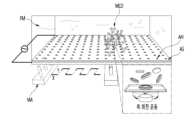
- FIG. 1A is a diagram schematically depicting a Magnetic force-assisted Dielectrophoretic Self-Assembly Technology (MDSAT) method according to an embodiment.
- MDSAT Magnetic force-assisted Dielectrophoretic Self-Assembly Technology
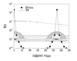
- Figure 1b shows the DEP and magnetic force distribution data between two adjacent assembly holes (AH).
- Figure 2a is an exemplary diagram of the relationship between the DEP force depending on the inclination angle on the surface of the assembly substrate (AS) of the micro-LED on the surface of the assembly hole (AH) in the embodiment.
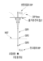
- FIG. 2B is a first data graph of the relationship between magnetic force (MGF) and dielectrophoretic force (DEP) to prevent color mixing in a display device according to an embodiment.
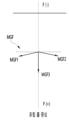
- FIG. 2C is a second data graph of magnetic force (MGF) for a semiconductor light emitting device in a display device according to an embodiment.
- MMF magnetic force
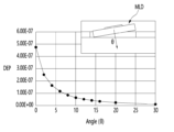
- Figure 2d shows data on the dielectrophoretic force acting on the assembled micro LED (MLD).
- Figure 3 is an exemplary diagram of a micro LED device according to an embodiment.
- Figure 4 shows simulation result data of the DEP force vector for assembly angle (0-180°) relative to the assembly hole surface for various micro-LEDs.
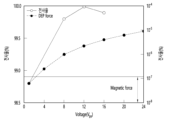
- Figure 8a shows transcription yield data related to DEP force and magnetic force.
- Figure 8b shows transfer yield data related to back metal thickness and magnetic force.
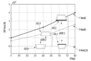
- Figure 8c shows comparison data of forward and reverse DEP forces depending on the presence or absence of a lower metal layer on the LED chip.
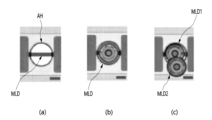
- 9A to 9C are diagrams showing the assembly state of the micro LED according to the relationship between magnetic force and DEP force.
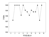
- Figure 10 shows experimental result data for evaluating the reproducibility of transcription yield.
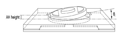
- Figure 12 is a schematic diagram showing the inclination angle between the micro-LED and the assembly hole with mismatched shapes.
- Figure 13 shows data on DEP force for shape-mismatched microLEDs as a function of assembly hole height.
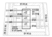
- Figure 15a is a schematic diagram of a PM panel showing red, green and blue LEDs and the interconnections between the LEDs and pads.
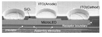
- Figure 15b is a cross-sectional view of the RGB panel.
- Figure 15c is a diagram showing I-V characteristics of red, green, and blue.
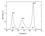
- Figure 15d is EL spectrum data showing emission peaks at 451 nm, 532 nm and 630 nm, respectively.
- Figure 17 shows change data of DEP force according to frequency.
- Figure 18 shows variation data of DEP force with frequency using RGB micro LED with bottom metal layer.
- 19 is a schematic diagram of a 3D model for COMSOL simulation.
- Display devices described in this specification include digital TVs, mobile phones, smart phones, laptop computers, digital broadcasting terminals, personal digital assistants (PDAs), portable multimedia players (PMPs), navigation, and slates.
- PDAs personal digital assistants
- PMPs portable multimedia players
- slates may include PCs, tablet PCs, ultra-books, desktop computers, etc.
- the configuration according to the embodiment described in this specification can be applied to a device capable of displaying even if it is a new product type that is developed in the future.
- FIG. 1A is a diagram schematically depicting a Magnetic force-assisted Dielectrophoretic Self-Assembly Technology (MDSAT) method according to an embodiment.
- MDSAT Magnetic force-assisted Dielectrophoretic Self-Assembly Technology
- Figure 1a shows the micro LED (MLD) and assembled substrate (AS) placed in a bath chamber using deionized water as the fluid medium (FM).
- an assembled substrate (AS) and a micro-LED are placed in a bath chamber, and a micro-LED cluster can be formed by axial rotational movement of a magnet under the assembled substrate, as shown in the inserted figure.
- the magnet can move in the direction of the arrow while maintaining axial rotational motion.
- the magnet array (MA) may be disposed along the back side of the assembly substrate (AS) to apply magnetic force to a micro-LED (MLD) embedded with a ferromagnetic material, for example, nickel.
- the magnet array (MA) may include a plurality of circular magnet rod arrays, but the embodiment is not limited thereto. The manufacturing method of micro-LED will be described later.
- the micro-LED is shown as being disposed on the upper side of the assembled substrate (AS), but the embodiment is not limited thereto.
- a micro-LED may be placed on the underside of the assembled substrate (AS).
- the micro-LED cluster moves in response to the magnetic force of the magnet array (MA), and when it approaches the assembly hole (AH), each micro-LED in the cluster moves to each assembly hole (AH) by the DEP force. ) is trapped.
- Figure 1b shows the DEP and magnetic force distribution between two adjacent assembly holes (AH).
- the essential magnetic force and DEP are indicated by dotted and solid lines, respectively, and the circuit diagram in the background of the graph indicates where the magnetic force and DEP are calculated.
- DEP forces can exceed magnetic forces by about 10 times and can control the final assembly process.
- DEP is a short-range force, so it can be controlled so that it can be effectively exerted around the assembly hole (AH).
- magnetic forces can act over long distances and help move micro-LEDs across the assembled substrate (AS).
- FIG. 2A is an exemplary diagram showing the relationship between the DEP force depending on the inclination angle on the surface of the assembly substrate (AS) of the micro-LED on the surface of the assembly hole (AH) in the embodiment.
- the metal layer (B-metal) on the back of the micro-LED moves toward the assembly electrode (AE).
- FIG. 2B is a first data graph of the relationship between magnetic force (MGF) and dielectrophoretic force (DEP) to prevent color mixing in a display device according to an embodiment.
- FIG. 2C is a second data graph of magnetic force (MGF) for a semiconductor light emitting device in a display device according to an embodiment.
- MMF magnetic force
- the exclusive-shaped design reference chip for example, a circular chip
- the dielectrophoretic force (DEP) and magnetic force (MGF) acting on the chip are relatively controlled to minimize mixed color assembly.
- DEP dielectrophoretic force
- MMF magnetic force
- the assembly surface of the LED chip is partially in contact with one side of the assembly electrode (AE) inside the assembly hole, and the dielectrophoretic force acting on the LED chip at the minimum angle that the LED chip has due to the height of the assembly hole (AH).
- AE assembly electrode
- AH height of the assembly hole
- the dielectrophoretic force acting on the micro LED is made into a smaller force than the magnetic force due to the height of the assembly hole, making it easy to break away and causing defects.
- the total force acting on the micro LED can be expressed as the vector sum of dielectrophoretic force (DEP) and magnetic force (MGF).
- FIGS. 2B and 2C can represent the assembly force that acts in the process of assembling micro LEDs of about 38 ⁇ m to 10 ⁇ m in size.
- the strength of the magnet may be about 250 to 500 mT, and a Ni magnetic material with a thickness of about 50 nm to 1000 nm may be introduced into the lower metal layer having a specific pattern, but is not limited thereto.
- the magnetic force acting on the micro LEDs forming a cluster at the closest distance to the magnet may be the third magnetic force (MGF3), which is the vector sum of the first magnetic force (MGF1) and the second magnetic force (MGF2),
- the third magnetic force (MGF3) may be about 1.2E-7 N, but is not limited thereto.
- the advantages of introducing magnetic force into the assembly of micro LEDs in a fluid include 1) forming a cluster of micro LEDs that can be moved in a desired direction, and 2) rotating the magnet so that the micro LEDs in the cluster can be continuously oriented in a random direction. 3) The magnetic force acting on the micro LED can be controlled by the amount of magnetic mass within the micro LED, 4) By introducing multiple magnets, it is possible to produce a large-area panel by increasing the assembly speed and assembly area, etc. There is.
- the magnetic force acting on the micro LEDs formed in a cluster by a magnet can be controlled to be constant at least within the cluster.
- the magnetic force acting on the micro LED can be controlled by the strength of the magnet, the distance from the magnet, and the amount of magnetic material contained in the micro LED.
- the magnet of the embodiment may employ a neodymium magnet with a strength of about 250-500 mT, and the closest distance between the micro LED and the magnet may correspond to the thickness of the assembled substrate.
- the magnetic force acting on each micro LED having an exclusive shape has the technical effect of controlling the magnetic pattern (area) and thickness of the micro LED so that similar magnetic force is applied even if the shape is different.
- the thickness of the magnetic mass included in the LED may be about 50 nm to 1,000 nm, and when a 500mT magnet is adopted, when the diameter of the LED chip is about 38 ⁇ m, the magnetic force applied to the LED chip is about 1.3280E-7 to about 1.3280E-7. It could be 4.2786E-7.
- the diameter of the LED chip is about 30 ⁇ m
- the thickness of the magnetic mass included in the LED is about 50nm to 1,000 nm
- the magnetic force applied to the LED chip is about 7.6923E-8 to 2.3230E-7. It can be.
- the diameter of the LED chip is about 20 ⁇ m
- the thickness of the magnetic mass included in the LED is about 50nm to 1,000 nm
- the magnetic force applied to the LED chip is about 3.4684E-8 to 8.6575E-8. It can be.
- the magnetic force applied to the LED chip is about 5.8394E-9 to 1.7415E. It could be -8.
- the diameter of the LED chip is about 38 ⁇ m
- the thickness of the magnetic mass included in the LED is about 50nm to 1,000 nm
- the magnetic force applied to the LED chip is about 3.3199E-8 to 1.0697E- It could be 7.
- the magnetic force applied to the LED chip is about 1.9231E-8 to 5.8075E. It could be -8.
- the diameter of the LED chip is about 20 ⁇ m
- the thickness of the magnetic mass included in the LED is about 50nm to 1,000 nm
- the magnetic force applied to the LED chip may be about 8.6710E-9 to 2.1644E-8.
- the magnetic force applied to the LED chip is about 1.4598E-9 to 1 4.3537E- It could be 9.
- FIG. 2b it is a graph of dielectrophoretic force (DEP) according to the position of the LED chip.
- the advantages of introducing dielectrophoretic force in assembling micro LEDs in a fluid are: 1) the dielectrophoretic force acting on the micro LED can be controlled by externally applied voltage and frequency; 2) the dielectrophoretic force acting on the micro LED is , the assembly direction can be controlled by designing the constituent materials of the micro LED surface facing the assembly electrode.
- the dielectrophoretic force acting on the micro LED acts very locally on the assembly electrode inside the assembly hole, and when the micro LED is away from the assembly electrode (AE), the dielectrophoretic force acting is very local. It is small and the direction of the acting force may not be in the assembly direction.
- the first dielectrophoretic force DEP1 may be applied when the LED chip is located on the surface of the assembly hole AH.
- the first dielectrophoretic force (DEP1) acting on the micro LED due to the height of the assembly hole is made to be a force smaller than the magnetic force (MGF).
- the second dielectrophoretic force (DEP2) can be applied when the LED chip is in contact with one electrode of the assembled electrode (AE) at a first angle.
- the first angle when assembly starts while matching may be about 6°
- the second dielectrophoretic force (DEP2) is about 1.18E-7. It may be N, but is not limited to this.
- the conditions for applying dielectrophoretic force may be a voltage of 6V, a frequency of 100kHz, and the spacing between assembled electrodes may be about 7.5 ⁇ m, but are not limited thereto.
- the vector direction of the magnetic force (MGF) and the second dielectrophoretic force (DEP2) applied to the LED chip at the point where it is aligned and assembled can be controlled to have a similar direction, which is the direction of the assembly hole.
- the magnetic force (MGF) applied to the LED chip at the point where it is aligned and assembled may be about 1.2E-7 N
- the second dielectrophoretic force (DEP2) may be about 1.18E-7 N.
- the total force applied to the LED chip at the point where it is aligned and assembled may be the sum of the magnetic force (MGF) and the second dielectrophoretic force (DEP2).
- the third dielectrophoretic force (DEP3) can be applied when the LED chip is properly assembled in the assembly hole. Accordingly, the total force applied to the LED chip when assembled may be the sum of the magnetic force (MGF) and the third dielectrophoretic force (DEP3).
- FIG 2d is data on the dielectrophoretic force acting on the assembled micro LED (MLD) (see Figure 4).
- the overlapped state can be considered a trapped state regardless of the overlap area for both assembly electrodes, and this point can be said to be the point of assembly.
- the minimum angle that the LED can have at a specific point is determined by the height of the assembly hole (AH). As the LED is aligned, the minimum angle becomes smaller, and as the minimum angle decreases, the dielectrophoretic force acting increases. I do it.
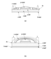
- Figure 3 is an exemplary diagram of a micro LED device according to an embodiment.
- Figure 3(a) is an exemplary diagram of a Blue or Green micro LED device according to the first embodiment.
- the blue or green micro LED device may include undoped GaN (u-GaN), n-type GaN (n-GaN), an active layer (not shown), and p-type GaN (p-GaN).
- the Blue or Green micro LED device includes a bottom metal (B-metal) under undoped GaN (u-GaN), and an n-type contact electrode (n) on n-type GaN (n-GaN).
- -contact may include a p-type contact electrode (p-contact) and passivation (PV) on p-type GaN (p-GaN).
- the n-type contact electrode (n-contact) and the passivation (PV) may be spaced apart by a predetermined distance (S).
- the blue or green micro LED device according to the first embodiment may be a GaN-based disk, and the lower metal (B-metal) may include Ti, but is not limited thereto.
- the p-type contact electrode may be formed of ITO, but is not limited thereto.
- n-type contact electrode may be formed of a single layer or a composite layer of Cr, Ti, and Ni.
- the thickness of undoped GaN may be about 3.0 to 4.0 ⁇ m. Additionally, the thickness of n-type GaN (n-GaN) may be about 3.0 to 4.0 ⁇ m. Additionally, the thickness of p-type GaN (p-GaN) may be about 0.2 to 1.0 ⁇ m.
- the thickness of the lower metal (B-metal) may be about 50 to 200 nm.
- the passivation (PV) may include SiO 2 and its thickness may be about 300 to 800 nm.
- Figure 3(b) is an exemplary diagram of a Red micro LED device according to the second embodiment.
- Red micro LED device includes n-type GaInP (n-GaInP), n-type GaAs (n-GaAs), n-type AlInP (n-AlInP), active layer (not shown), p-type GaP (p- GaP) may be included.
- n-GaInP n-type GaInP
- n-GaAs n-type GaAs
- n-AlInP n-type AlInP
- active layer not shown
- p-type GaP p- GaP
- the Red micro LED device has a bottom metal (B-metal) under n-type GaInP (n-GaInP), and an n-type contact electrode (n-) on n-type AlInP (n- AlInP). contact), and may include a p-type contact electrode (p-contact) and passivation (PV) on p-type GaP (p-GaP).
- the n-type contact electrode (n-contact) and the passivation (PV) may be spaced apart by a predetermined distance (S).
- the Red micro LED device according to the second embodiment may be a GaAs-based disk, and the lower metal (B-metal) may include Ti, but is not limited thereto.
- n-type contact electrode may be formed of a single layer or a composite layer of Au, AuGe, Ti, and Ni.
- the p-type contact electrode may be formed of ITO, but is not limited thereto.
- the thickness of n-type GaInP may be about 0.1 to 0.5 ⁇ m.
- n-type GaAs may be about 0.02 to 0.10 ⁇ m. Additionally, the thickness of n-type AlInP (n-AlInP) may be about 3.0 to 5.0 ⁇ m. Additionally, the thickness of p-type GaP (p-GaP) may be 0.5 to 1.5 ⁇ m.
- the thickness of the lower metal (B-metal) may be about 50 to 200 nm.
- the passivation (PV) may include SiO 2 and its thickness may be about 300 to 800 nm.
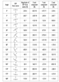
- Figure 4 shows simulation result data of the DEP force vector for assembly angle (0-180°) relative to the assembly hole surface for various micro-LEDs.
- CM Clausius-Mossotti
- Figure 2 shows the Z-axis component of the DEP force vector in the assembled electrode (AE) direction and cross-sectional views showing the position of the micro-LED for angles 0-90° and 90-180°. is inserted.
- Figure 2 shows that the DEP force increases as the angle decreases. This indicates that as the angle decreases, the micro-LED is pulled into the assembly hole and is eventually assembled when the angle is less than 10° when the DEP force dominates the magnetic force.
- the axial rotation of the magnet in the proposed MDSAT method which induces the rocking motion of the microLED, is expected to increase the likelihood that the microLED will meet this angular criterion for assembly.
- the DEP force fluctuates around 0 when the angle exceeds 60° and becomes clearly negative after 165°. This indicates that the micro-LED is likely to be pushed out of the assembly hole (AH) at an angle of more than 60°, especially in the presence of external magnetic force.
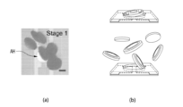
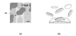
- Figures 5(a) and 5(b) show stage 1 in which micro LEDs are gathered around the assembly hole (AH) in response to the movement of magnetic force.
- the micro-LED closest to the assembly hole (AH) responds to the generated DEP force, and its edge touches the perimeter of the assembly hole.
- Figures 6(a) and 6(b) show the second stage in which the micro LED swings along the edge of the assembly hole (AH) in response to the rotational movement of the magnet. This indicates that it is in a transition state where there is a balance between DEP and magnetic force.
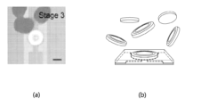
- Figures 7(a) and 7(b) show that the micro-LED is assembled as the angle between the micro-LED and the assembly hole (AH) falls below a certain angle.
- the transfer yield was studied as the applied peak-to-peak voltage (Vpp) relative to the DEP was varied based on the specified operation of the micro LED in the assembly hall (AH).
- Figure 8a provides the experimentally obtained transfer yields along with the DEP force and magnetic force calculated from COMSOL simulations.
- the magnetic force was calculated at 10 locations around the assembly hall (AH), and the results ranged from 1 ⁇ 10 -8 [N] to 1.2 ⁇ 10 -7 [N].
- the size of the assembled board is approximately 75 mm ⁇ 75 mm and approximately 270 ⁇ 240 pixels.
- the assembly board consists of approximately 64,800 assembly holes (AH), spaced 278 ⁇ m apart from each other.
- Figure 8b shows transfer yield data related to the thickness of the back metal and magnetic force.
- the micro LED is effectively moved using magnetic force in the fluid, and the assembly direction is perfectly controlled by assembling the disk-shaped LED chip with the back metal using DEP force, thereby increasing the assembly rate or transfer rate.
- the assembly direction is perfectly controlled by assembling the disk-shaped LED chip with the back metal using DEP force, thereby increasing the assembly rate or transfer rate.
- Figure 8c shows comparison data of forward and reverse DEP force depending on the presence or absence of a lower metal layer on the LED chip.
- the LED chip (LED_E) according to the embodiment may have a lower metal at the bottom of the chip.
- the LED (LED_R) according to the comparative example may not have a lower metal at the bottom of the chip.
- the semiconductor light emitting device has a rear metal layer, so that it is more advantageous to distinguish the chip from top to bottom, and thus the assembly direction can be perfectly controlled.
- the DEP force during forward assembly is significantly increased by more than 50% compared to the DEP force during reverse assembly.
- the LED chip (LED_E) may have a rear metal, and the difference between the DEP force when a reverse electric force is applied and the DEP force when a 7V forward electric force is applied ( ⁇ DEP_E) may be about 3.0
- the difference ( ⁇ DEP_R) between the DEP force when reverse electric force is applied and the DEP force when 7V forward electric force is applied may be about 2.0X10 -6 [N].
- the semiconductor light emitting device has a rear metal layer, so that it is more advantageous to distinguish the top and bottom of the chip, and this has the special technical effect of perfectly controlling the assembly direction.
- Table 1 below shows data on the thickness, weight, and ratio of Ni according to the strength of the magnet in the examples.
- a semiconductor light emitting device may include a back metal layer, and the back metal layer may include a magnetic material.
- the embodiment may include Ni as the metal layer, but is not limited thereto.
- Table 1 shows the Ni thickness and the corresponding Ni ratio change data to have a magnetic force of about 1.2E-7[N] (see FIG. 1b), depending on the strength of the magnet.
- the magnetic force used to assemble the 38 ⁇ m-class DSAT may be about 1.2E-7[N].
- the ratio of Ni in a semiconductor light emitting device chip may be about 0.25% to 36.75%.
- the experimental conditions in the example may be 12Vpp, frequency 100kHz, 430mT Neodymium magnet of 2mmx20mm size, and the distance between the micro LED and the magnet may be about 504.78 ⁇ m.
- the thickness of the glass may be about 500 ⁇ m, and the thickness of the electrode and passivation may be about 0.28 ⁇ m.
- the height of the assembly hole may be about 4.5 ⁇ m, the thickness of the magnetic material (Ni) of the GaN-based LED may be 220nm, and the electrode gap may be about 7.5 ⁇ m, but is not limited thereto.
- the DEP force may be about 10 times greater than the magnetic force, for example, about 12 times greater.
- the DEP force may be about 1.47E-6 [N] (FIG. 1b), and the magnetic force may be about 1.2E-7 [N], but are not limited thereto.
- Figures 9a to 9c are diagrams showing the assembly state of the micro LED according to the relationship between magnetic force and DEP force.
- Figure 10 shows experimental result data for evaluating the reproducibility of transcription yield.
- Figure 9(a) shows the initial stage where the magnetic force dominates the DEP force. For example, it is shown that the micro LED seated in the assembly hole location is swept away by the movement of the magnet, resulting in an unassembled position as shown in FIG. 9(a).
- Figure 9(b) shows that as the Vpp and DEP forces increase to levels above the magnetic force, the empty assembly hole (AH) is gradually filled with micro-LED (MLD) and remains stable.
- Figure 9(c) shows that the transcription yield began to decrease after reaching 12Vpp.
- the decrease in transfer yield is due to a defect in which multiple micro-LEDs (MLD1, MLD2) are arranged around one assembly hole (AH), as shown in Figure 9(c).
- a gap may appear between the micro-LED and the assembly hole (AH) wall due to design tolerances.
- the assembly hole (AH) matched the shape of each RGB micro-LED, and the size of the assembly hole (AH) was designed to be 4 ⁇ m larger than the LED in both axes.
- Red micro-LED has a diameter of 42 ⁇ m
- Green micro-LED has a diameter of 49 ⁇ m ⁇ 35 ⁇ m
- Blue micro-LED has a diameter of 56 ⁇ m ⁇ 28 ⁇ m. .
- R-MLD red micro LED
- G-MLD green micro LED
- B-MLD blue micro LED
- Figure 11 is an image of three examples of shape mismatch defects.
- a blue micro-LED (B-MLD) seated inside (G-AH) is shown, with the anode and cathode also indicated.
- Figure 12 is a schematic diagram showing the inclination angle between the micro-LED and the assembly hole whose shape does not match.
- one side of the micro LED was located at the bottom corner of the assembly hole and the other diagonal was placed above the assembly hole.
- ⁇ i can be defined as the inclination angle between the micro LED and the assembly hole.
- Figure 13 is a data plot for DEP force for shape-mismatched micro LEDs as a function of assembly hole height.
- the maximum value of the magnetic force acting on the micro LED was calculated to be 1.2 ⁇ 10 -7 [N] based on COMSOL simulation and reflected in the chart.
- This minimum angle is ultimately determined by the assembly hole height, and the dielectrophoresis force at the minimum angle can be determined.
- the dielectrophoretic force formed by the minimum angle that the micro LED can have in the mixed color mode decreases as the assembly hole height increases, and the positive assembly rate can increase accordingly. there is.
- the magnetic force and dielectrophoretic force can be controlled, the direction of the magnetic force can be at least in the direction toward the bottom of the assembly substrate, and the dielectrophoretic force can have force in the assembly direction when the micro LED is assembled in the assembly hole. there is.
- whether the magnetic force or dielectrophoretic force will be dominantly influenced can be complexly controlled depending on the position of the LED chip.
- the circular chip which is the reference chip for the exclusive structure design
- the dielectrophoretic force is controlled to be the same as the magnetic force at the angle of the reference chip provided by the assembly hole, all color mixing defect modes are assembled.
- the dielectrophoretic force can be controlled to be smaller than the magnetic force.
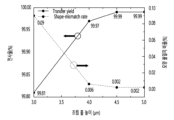
- Figure 14 is data on transfer yield as a function of assembly hole height in an example.
- the transfer yield was investigated as a function of the assembly hole height in the range of 3 ⁇ m to 5 ⁇ m, and the results are shown in FIG. 14.
- the size of the assembled board was 75mm ⁇ 75mm and consisted of 64,800 RGB assembly holes spaced 278 ⁇ m apart from each other.
- the magnet head which is the same size as the assembly board, consists of an 8 ⁇ 8 magnet array, and each magnet is designed to synchronously scan a 13 mm ⁇ 13 mm area for 15 minutes.
- each neodymium magnet bar (diameter: 5 mm, length: 20 mm) is 5000 gauss.
- the magnetic array can move at 250 ⁇ m/s in both x and y directions while rotating axially at 420 revolutions per minute.
- a 100mm x 100mm RGB micro LED display panel was manufactured using the MDSAT method. Previous studies reported the implementation of FSA-based micro LED displays, but they were based on monochromatic LEDs.
- the panel according to the embodiment consists of 43,200 micro LEDs corresponding to a display resolution of 120 ⁇ 120 pixels and a pixel pitch of 834 ⁇ m.
- Figure 15a is a schematic diagram of a PM panel showing red, green and blue LEDs and the interconnections between the LEDs and pads.
- Figure 15b is a cross-sectional view of the RGB panel.
- Figure 15b shows a focused ion beam (FIB) image of a cross-section of a PM panel showing two coplanar assembly electrodes, microLEDs in assembly holes, planarization layer, and power lines.
- FIB focused ion beam
- the assembly holes are shown as white dashed lines because they are faintly visible due to similar contrast between the organic materials.
- a spray process was performed to fix the micro LED after self-assembly. Then, planarization was performed and contact holes were made to connect the power lines and pads for the anode and common electrode.
- Figure 15c is a picture showing the I-V characteristics of red, green, and blue.
- Figure 15c shows the I-V characteristics of red, green, and blue micro LEDs with forward voltages of 1.83, 2.3, and 2.65 V, respectively, at leakage currents of less than 10 ⁇ A and 10 nA.
- Figure 15d provides the EL spectrum showing emission peaks at 451 nm, 532 nm, and 630 nm, respectively.
- the embodiment exhibits electroluminescence (EL) light emission of an RGB panel with excellent light emission intensity and luminance uniformity, and it is possible to implement 3 ⁇ 3 pixels that clearly emit red, green, and blue light.
- EL electroluminescence
- the panel showed a 99.98% emitting pixel yield with 10 defective pixels.
- the scalable MDSAT method can also potentially be integrated with existing active matrix (AM) backplanes by adjusting the magnet array size accordingly.
- AM active matrix
- RGB micro LEDs can be deposited on a transistor backplane with a front-emitting structure. The anode of the micro LED can then be connected to the driving circuit of the AM backplane and the cathodes connected together.
- RGB LED DEP power difference between AlGaInP-based and GaN-based LEDs
- Table 2 shows the input parameters for COMSOL: material, permittivity, and conductivity. Thin layers of multiple quantum wells (MQWs) were not included in COMSOL simulations because they were expected to have minimal impact on the results.
- MQWs multiple quantum wells
- DSAT has another major potential for simultaneously assembling RGB micro-LEDs by matching the shapes of the RGB LEDs to each assembly hole.
- RGB LED can be transferred at once in a single chamber, which has the advantages of simplifying system design, reducing investment costs, and minimizing process costs.
- round and oval shapes are more resistant to damage from LED-to-LED collisions due to their rounded shape compared to edged shapes (such as triangles, squares, or rectangles).
- the design rule was set to 7 ⁇ m, which means that 35 ⁇ m is needed for three areas for three contact points and two spaces between contact points.
- the purpose of separation is to eliminate the formation of LED-to-LED chains due to magnetization after self-assembly, as illustrated in Figures 3(a) and 3(b).
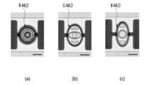
- Figure 16 is a microscope image of an RGB micro LED according to an embodiment.
- Figure 16 (a) is an image of an AlGaInP-based red LED with a micro LED size of 38 ⁇ m in diameter.
- Figure 16 (b) is an image of a GaN-based green LED with a micro LED size of 45 ⁇ m ⁇ 31 ⁇ m.
- Figure 16 (c) is an image of a GaN-based blue LED with a micro LED size of 52 ⁇ m ⁇ 24 ⁇ m (scale bar is 20 ⁇ m).
- the separation (S) was set to 1.5 ⁇ m on both sides (left and right) of the micro-LED. Therefore, the diameter of the red micro-LED (R-MLD) was set to 38 ⁇ m considering the design rule (35 ⁇ m) and the two separations (3 ⁇ m).
- the oval shape of the green micro-LED was designed to be 45 ⁇ m ⁇ 31 ⁇ m.
- the long and short axes are respectively 7 ⁇ m larger and 7 ⁇ m smaller than the 38 ⁇ m diameter of the circular-shaped red micro LED.
- the 45 ⁇ m long axis was determined based on process tolerances based on the photolithography and etching steps used to fabricate the micro LEDs and assembly holes.
- the assembly hole diameter of the circular-shaped red micro LED was 42 ⁇ m, and the process tolerance was about 3 ⁇ m.
- the long axis of the green micro-LED was selected at 45 ⁇ m to prevent the green micro-LED from being trapped in the circular assembly hole of the red micro-LED.
- the oval shape of the blue micro-LED was designed in the same way that the green micro-LED was determined.
- the long axis and short axis are respectively 7 ⁇ m larger and 7 ⁇ m smaller than the 45 ⁇ m ⁇ 31 ⁇ m of the green micro-LED (B-MLD), and as a result, the oval shape of the blue micro-LED was designed to be 52 ⁇ m ⁇ 24 ⁇ m as shown in (c) of Figure 16.
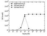
- Figures 17 and 18 show data on the DEP force from COMSOL simulation.
- Figure 17 shows change data of DEP force with frequency at a fixed value of applied voltage (12 Vpp).
- Figure 18 shows the variation data of DEP force with frequency at a fixed value of applied voltage (12 Vpp) using a modified RGB micro LED with a bottom metal layer on the bottom surface.
- Figure 17 shows the change in DEP power of RGB micro LED according to frequency.
- the applied voltage and the gap between the two assembled electrodes are fixed to 12 Vpp and 7.5 ⁇ m, respectively. These were found to be the optimal conditions used in manufacturing display panels.
- the three LEDs experience the highest DEP force at approximately 100 kHz.
- the DEP force decreases above 100 kHz, while AlGaInP-based LEDs maintain the DEP force. Under this condition, all three LEDs cannot be assembled simultaneously with high yield because the frequency response of the DEP force is different.
- the DEP force is applied to a polarizable particle in a non-uniform electric field, it is affected by the electric field magnitude, the frequency of the input voltage, the permittivity and conductivity of the particle (i.e. micro-LED), and the particle size (i.e. micro-LED chip size). Receive.
- the difference in frequency response is due to the difference in conductivity between layer 4 of the AlGaInP-based and layer 3 of the GaN-based LED, and is shown in Table 2. This can be explained by the CM factor, which is a frequency function that includes both dielectric ( ⁇ 0 ⁇ r ) and conductive contributions ( ⁇ ).
- micro-LEDs for the modified GaN-based and AlGaInP-based micro-LEDs are illustrated in Figures 3(a) and 3(b).
- the DEP power is improved for all LEDs, especially at high frequencies above 100 kHz, GaN-based blue and green LEDs do not show a DEP power drop.
- the common assembly frequency of RGB LEDs can be optimized over a wide frequency range depending on the configuration and design of the assembly board.
- Adding a lower metal layer can maximize the difference in conductivity between the top and bottom surfaces of the micro LED, improving the ratio of the DEP force applied to the bottom surface to the top surface by approximately 1.5 times.
- the micro LED structure with an added bottom metal layer has a special technical effect that improves MDSAT's ability to select the right LED surface for assembly.
- the electrode gap (distance between two assembled electrodes) and the dielectric layer of the assembled electrode which are factors that affect the electric field size of the assembled substrate and the size of the LED chip, were investigated.
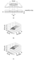
- 19 is a schematic diagram of a 3D model for COMSOL simulation.
- Figure 19 illustrates three factors that affect DPE force: the micro LED chip, the electrode gap, and the dielectric layer on the assembled electrode.
- the LED chip according to the embodiment may include a lower metal layer such as titanium on the bottom surface and may include a GaN-based micro LED having a cylindrical shape.
- the diameter of the micro LED can range from 10 to 50 ⁇ m to evaluate the effect of LED chip size on the DEP force.
- the examples use 'gap ratio' instead of 'electrode gap' to investigate the independent influence of two factors (electrode gap and LED chip size) on DEP force. can be used.
- 'Gap ratio' is defined as the ratio of the distance between two assembled electrodes to the micro LED chip size, and 'electrode gap' is the distance between two assembled electrodes.
- Figure 19(b) shows the variation of DEP force with respect to LED size and gap ratio for SiO 2 dielectric layer and Figure 19(c) Si 3 N 4 dielectric layer.
- Figures 19(b) and 19(c) show that as the LED chip size increases, the DEP force increases and the gap ratio for both SiO 2 and Si 3 N 4 dielectric layers decreases.
- Figures 19(b) and 19(c) show that the dielectric layer on the assembled substrate (AS) is an essential element affecting the DEP force.
- Materials with a high dielectric constant e.g. Si 3 N 4 dielectric layer
- the MDSAT method according to the embodiment utilizes magnetic force to effectively transfer micro-LEDs, thereby dramatically improving transfer yield and allowing the two forces (magnetic force and DEP force) to be controlled to compete with each other during assembly. Therefore, when the assembly process occurs near the assembly hole, the DEP force can be controlled to be larger than the magnetic force.
- the magnetic force acting on the micro-LED varies depending on the distance between the micro-LED and the magnet and can range from 1 ⁇ 10 -8 [N] to 1.2 ⁇ 10 -7 [N].
- the DEP force near the assembly hole can be controlled to be greater than 1.2 ⁇ 10 -7 [N].
- the DEP force should be higher than 1.2
- the inability to assemble was studied.
- the electrode gap and LED chip size can be selected at about 7.5 ⁇ m and about 38 ⁇ m, respectively, considering the process margin at the assembly electrode on the assembly board and the power line at the top of the LED chip, but are not limited to these.
- an assembly board can be manufactured.
- a triple layer of Mo/Al/Mo (20/100/20 nm) was deposited via e-beam evaporation and patterned to define the assembled electrode area.
- photoresist DNR L-300, DONGJIN SEMICHEM
- DNR L-300, DONGJIN SEMICHEM photoresist
- the substrate was baked at 110°C for 2 minutes.
- the Mo/Al/Mo layer was then wet etched using aluminum etchant for 10 minutes, and the substrate was rinsed with deionized water.
- the Si 3 N 4 dielectric layer of the assembled electrode was deposited by plasma enhanced chemical vapor deposition (PECVD).
- PECVD plasma enhanced chemical vapor deposition
- Photoresist WPR-1052, JSR
- WPR-1052, JSR photoresist
- a developer AZ-300MIF, MERCK
- micro LED After assembling the micro LED on an assembly board, spray a layer of photoresist (DPA-5000, DONGJIN SEMICHEM) to fix the micro LED, then soft bake at 100°C for 2 minutes, UV expose without a photomask, and bake in the oven. Bake at 200°C for 15 minutes.
- a layer of photoresist DPA-5000, DONGJIN SEMICHEM
- a layer of photoresist (SU-8, MICROCHEM) was spin-coated on the assembled substrate at 3000 rpm for 30 seconds. SU-8 was then baked in an oven at 200°C for 1 hour.
- a photoresist (GXR601, MERCK) was rotated onto the photoresist (SU-8, MICROCHEM) and patterned into a circular shape to form the n-contact and p-contact on the micro-LED. defined.
- RIE Reactive Ion Etching
- the passivation layer (SiO 2 ) of the micro-LED was etched within the contact hole.
- a transparent power line made of ITO Indium Tin Oxide
- ITO Indium Tin Oxide
- the ITO layer was deposited on patterned photoresist (DNR L-300, DONGJIN SEMICHEM).
- DNR L-300 is then removed using acetone to peel off the overlying ITO layer, creating a transparent power line.
- Ti/Al power line was also manufactured using a lift-off process.
- the powerline was patterned by depositing a Ti/Al bilayer using e-beam onto patterned DNR L-300.
- GaN-based micro LEDs can be manufactured.
- a GaN-based epi layer was prepared on a sapphire wafer and ITO was deposited on it.
- photoresist GXR601, MERCK
- ITO a GaN-based epi layer
- soft baking 100 °C for 2 min
- exposing to UV and using a developer (AZ-300MIF, MERCK).
- developer AZ-300MIF, MERCK
- the ITO/GaN-based epitaxial layer was etched using an inductively coupled plasma (ICP) etch device to form a mesa shape, and the remaining photoresist was peeled off.
- ICP inductively coupled plasma
- photoresist DNR L-300, DONGJIN SEMICHEM
- DNR L-300 DONGJIN SEMICHEM
- n-contact metal Cr/Ti/Ni/Ti, 20/20/100/70 nm was fabricated in the n region of the micro LED through electron beam deposition and lift-off processes.
- Figure 3(a) shows a schematic diagram of the n-contact metal.
- the Ni layer embedded in the n-contact metal can play a role in moving the micro-LED in response to magnetic force.
- SiO 2 passivation layer
- the passivation layer can improve hydrophilicity for free movement and prevent substrate adsorption (attachment of micro LEDs to the surface of the assembled substrate) and micro LED agglomeration. This has another advantage in that micro LEDs that are not assembled in the assembly hole can be recycled because there is no substrate adsorption. Additionally, the passivation layer spatially separates the Ni layer from the surface of the micro-LED and prevents the micro-LED from sticking to each other due to magnetization after magnetic manipulation.
- Photoresist (GXR601, MERCK) was coated and patterned on the micro LED, and then a PSA (pressure-sensitive adhesive) film was applied on top.
- a PSA (pressure-sensitive adhesive) film was applied on top.
- LLO laser-lift-off
- the micro LED on the PSA film was soaked in acetone to dissolve the patterned photoresist, and the micro LED was released from the PSA and dispersed in the acetone bath.
- AlGaInP-based micro LEDs can be manufactured.
- an ITO layer was deposited on an AlGaInP-based epi layer grown on a GaAs wafer.
- the next process involves fabricating the mesa and outline of the micro LED, and this process is similar to that of GaN-based micro LED.
- the same method was used for photolithography (spin coating, soft baking, UV exposure, development, and hard baking).
- the ICP etcher Using the same ICP etcher, the ITO/GaAs-based epitaxial layer was etched to form a mesa shape, and the remaining photoresist was peeled off.
- photoresist DNR L-300, DONGJIN SEMICHEM
- DNR L-300 DONGJIN SEMICHEM
- n-contact metal AuGe/Au/Ti/Ni/Ti, 100/100/50/100/50 nm
- a 500 nm thick silicon dioxide layer was applied to the side walls of the micro LED. deposited on the top surface.
- photoresist (GXR601, MERCK) was coated on the micro LED. The sides of the photoresist were then attached onto the glass wafer using silicone adhesive.
- a CLO (Chemical Lift-Off) process was performed to remove the GaAs wafer using a solution (NH 4 OH:H 2 O 2 :H 2 O), and then the passivation layer (SiO 2 ) formed between the micro LEDs was removed. It was removed by RIE.
- Assembly can occur with the assembly board facing down or in a position where the micro-LED is placed on the bottom of the bath beneath the board. In this case, a stronger magnetic force is needed to overcome gravity to pull the micro-LED up to the assembly board.
- the main advantage of this approach is that unintended particles, which most likely do not have magnetic properties, are excluded from the assembly process because they do not react to the magnetic field.
- an array of glass tubes (called magnetic tubes) containing magnetic rods are prepared to feed the micro LEDs.
- the magnetic rod moves vertically inward towards the end of the glass tube.
- the micro-LED is attached to or dropped from the end surface of the glass tube through the vertical movement of the magnet inside the glass tube.
- the amount supplied per magnetic tube is 2 to 3 mg in weight. According to the experimental example, there is no effect on assembly yield when the number of LEDs is 2 to 3 mg.
- An array of magnetic tubes can drop the LEDs directly onto the assembly board in the bath chamber. The magnetic tube array can be reused after the self-assembly process to collect LEDs for recycling and preparation for the next run.
- the MDSAT method has the advantage of being able to recycle micro LEDs.
- Embodiments may be adopted in the field of displays that display images or information.
- Embodiments may be adopted in the field of displays that display images or information using semiconductor light-emitting devices.
- Embodiments can be adopted in the field of displays that display images or information using micro- or nano-level semiconductor light-emitting devices.
Landscapes
- Led Devices (AREA)
- Devices For Indicating Variable Information By Combining Individual Elements (AREA)
Abstract
Description


Claims (10)
- 서로 이격된 제1 조립 전극과 제2 조립 전극;상기 제1, 제2 조립 전극 상에 배치된 유전체층;소정의 조립 홀을 구비하여 상기 유전체층 상에 배치되는 절연층;상기 조립 홀 상에 배치되는 반도체 발광소자를 포함하고,상기 조립 홀의 높이는 4.0 ㎛ 이상인, 반도체 발광소자를 포함하는 디스플레이 장치.
- 제1항에 있어서,상기 반도체 발광소자의 크기에 대한 상기 이격된 제1, 제2 조립 전극 사이의 거리 비율의 비율인 갭 비율이 0.4 내지 0.8인, 반도체 발광소자를 포함하는 디스플레이 장치.
- 제1항에 있어서,상기 조립 홀의 높이는 4.5 ㎛ 내지 5.0㎛인, 반도체 발광소자를 포함하는 디스플레이 장치.
- 제1항에 있어서,상기 유전체층은질화물을 포함하는, 반도체 발광소자를 포함하는 디스플레이 장치.
- 제3항에 있어서,상기 유전체층은Si3N4를 포함하는, 반도체 발광소자를 포함하는 디스플레이 장치.
- 제1항에 있어서,상기 반도체 발광소자는,제1 도전형 반도체층, 활성층 및 제2 도전형 반도체층을 포함하는 발광구조물;상기 제1 도전형 반도체층과 전기적으로 연결되는 제1 컨택 전극;상기 제1 도전형 반도체층 아래에 배치되는 메탈층;상기 제2 도전형 반도체층 상에 배치되는 제2 컨택 전극; 및상기 발광구조물 상에 배치되는 패시베이션층;을 포함하고,상기 메탈층은, 자성물질을 포함하는, 반도체 발광소자를 포함하는 디스플레이 장치.
- 제6항에 있어서,상기 반도체 발광소자의 무게 대비 상기 자성물질의 무게 비율은 0.25%~36.75%인, 반도체 발광소자를 포함하는 디스플레이 장치.
- 제6항에 있어서,상기 자성물질은Ni을 포함하는, 반도체 발광소자를 포함하는 디스플레이 장치.
- 제6항에 있어서,상기 자성물질의 두께는5nm 내지 2300nm인, 반도체 발광소자를 포함하는 디스플레이 장치.
- 제6항에 있어서,상기 제1 컨택 전극은상기 제2 컨택 전극의 둘레를 감싸면서 배치되며,상기 발광구조물의 상측이 일부 제거된 제1 도전형 반도체층과 전기적으로 연결된 것을 특징으로 하는, 반도체 발광소자를 포함하는 디스플레이 장치.
Priority Applications (4)
| Application Number | Priority Date | Filing Date | Title |
|---|---|---|---|
| EP23843417.9A EP4560691A4 (en) | 2022-07-21 | 2023-07-20 | DISPLAY DEVICE COMPRISING A SEMICONDUCTOR ELECTROLUMINESCENT ELEMENT |
| CN202380055274.8A CN119768911A (zh) | 2022-07-21 | 2023-07-20 | 包括半导体发光器件的显示装置 |
| US18/992,051 US20260013284A1 (en) | 2022-07-21 | 2023-07-20 | Display device comprising semiconductor light-emitting element |
| KR1020257002199A KR20250030482A (ko) | 2022-07-21 | 2023-07-20 | 반도체 발광소자를 포함하는 디스플레이 장치 |
Applications Claiming Priority (4)
| Application Number | Priority Date | Filing Date | Title |
|---|---|---|---|
| KR10-2022-0090286 | 2022-07-21 | ||
| KR20220090286 | 2022-07-21 | ||
| KR20230008185 | 2023-01-19 | ||
| KR10-2023-0008185 | 2023-01-19 |
Publications (1)
| Publication Number | Publication Date |
|---|---|
| WO2024019571A1 true WO2024019571A1 (ko) | 2024-01-25 |
Family
ID=89577108
Family Applications (2)
| Application Number | Title | Priority Date | Filing Date |
|---|---|---|---|
| PCT/KR2023/010530 Ceased WO2024019571A1 (ko) | 2022-07-21 | 2023-07-20 | 반도체 발광소자를 포함하는 디스플레이 장치 |
| PCT/KR2023/010531 Ceased WO2024019572A1 (ko) | 2022-07-21 | 2023-07-20 | 디스플레이 화소용 반도체 발광소자 및 이를 포함하는 디스플레이 장치 |
Family Applications After (1)
| Application Number | Title | Priority Date | Filing Date |
|---|---|---|---|
| PCT/KR2023/010531 Ceased WO2024019572A1 (ko) | 2022-07-21 | 2023-07-20 | 디스플레이 화소용 반도체 발광소자 및 이를 포함하는 디스플레이 장치 |
Country Status (5)
| Country | Link |
|---|---|
| US (2) | US12543412B2 (ko) |
| EP (2) | EP4560691A4 (ko) |
| KR (2) | KR20250034960A (ko) |
| CN (2) | CN119768911A (ko) |
| WO (2) | WO2024019571A1 (ko) |
Cited By (1)
| Publication number | Priority date | Publication date | Assignee | Title |
|---|---|---|---|---|
| GB2624970A (en) * | 2022-10-18 | 2024-06-05 | Lg Display Co Ltd | Display device |
Citations (5)
| Publication number | Priority date | Publication date | Assignee | Title |
|---|---|---|---|---|
| KR20060129801A (ko) * | 2005-06-13 | 2006-12-18 | 주식회사 비첼 | 발광다이오드 디스플레이소자 및 그 제조 방법 |
| KR20190063201A (ko) * | 2017-11-29 | 2019-06-07 | 한국생산기술연구원 | 자성물질을 구비하는 발광다이오드 소자 및 이의 제조방법 |
| KR20200026760A (ko) * | 2019-09-09 | 2020-03-11 | 엘지전자 주식회사 | 반도체 발광소자를 이용한 디스플레이 장치 |
| KR20200026766A (ko) * | 2019-11-11 | 2020-03-11 | 엘지전자 주식회사 | 반도체 발광소자를 이용한 디스플레이 장치의 제조방법 |
| WO2022097785A1 (ko) * | 2020-11-06 | 2022-05-12 | 엘지전자 주식회사 | 발광 소자 및 이를 포함하는 디스플레이 장치 |
Family Cites Families (17)
| Publication number | Priority date | Publication date | Assignee | Title |
|---|---|---|---|---|
| WO2001095375A1 (en) | 2000-06-06 | 2001-12-13 | The Penn State Research Foundation | An electro-fluidic assembly process for integration of electronic devices onto a substrate |
| US10418527B2 (en) | 2014-10-31 | 2019-09-17 | eLux, Inc. | System and method for the fluidic assembly of emissive displays |
| KR101730927B1 (ko) | 2016-07-21 | 2017-04-27 | 피에스아이 주식회사 | 휘도가 향상된 초소형 led 전극어셈블리 및 그 제조방법 |
| US10236324B1 (en) | 2017-09-15 | 2019-03-19 | Samsung Display Co., Ltd. | Full-color light emitting diode display having improved luminance and method of manufacturing the same |
| WO2019203405A1 (ko) * | 2018-04-19 | 2019-10-24 | 엘지전자 주식회사 | 반도체 발광 소자를 이용한 디스플레이 장치 및 이의 제조방법 |
| CN109216400B (zh) * | 2018-10-29 | 2020-11-24 | 厦门乾照光电股份有限公司 | Micro LED阵列器件的巨量转移装置及相关方法 |
| KR20200095210A (ko) | 2019-01-31 | 2020-08-10 | 엘지전자 주식회사 | 반도체 발광 소자, 이의 제조 방법, 및 이를 포함하는 디스플레이 장치 |
| KR102173349B1 (ko) | 2019-06-28 | 2020-11-03 | 엘지전자 주식회사 | 디스플레이 장치 제조를 위한 기판 및 디스플레이 장치의 제조방법 |
| EP3996139B1 (en) | 2019-07-01 | 2025-09-03 | LG Electronics Inc. | Display device using micro led, and manufacturing method therefor |
| KR102802778B1 (ko) * | 2019-12-11 | 2025-05-07 | 엘지전자 주식회사 | 마이크로 led와 관련된 디스플레이 장치 및 이의 제조 방법 |
| KR102802247B1 (ko) | 2020-01-22 | 2025-05-07 | 엘지전자 주식회사 | 반도체 발광소자를 이용한 디스플레이 장치 |
| KR102825756B1 (ko) | 2020-02-13 | 2025-06-27 | 엘지전자 주식회사 | 반도체 발광소자를 이용한 디스플레이 장치 |
| EP4187623A4 (en) | 2020-07-21 | 2024-04-17 | Lg Electronics Inc. | Semiconductor light-emitting device and display device using semiconductor light-emitting device |
| WO2022034937A1 (ko) | 2020-08-11 | 2022-02-17 | 엘지전자 주식회사 | 반도체 발광소자를 이용한 디스플레이 장치 및 이의 제조방법 |
| KR102870233B1 (ko) * | 2020-09-28 | 2025-10-14 | 엘지전자 주식회사 | 반도체 발광소자 및 이를 포함하는 디스플레이 장치 |
| KR102514025B1 (ko) | 2020-11-06 | 2023-03-24 | 고려대학교 산학협력단 | 마이크로 발광소자 구조 및 마이크로 발광소자 전사 방법 |
| US12598852B2 (en) | 2020-11-25 | 2026-04-07 | Lg Electronics Inc. | Light-emitting element and display device comprising same |
-
2023
- 2023-07-20 WO PCT/KR2023/010530 patent/WO2024019571A1/ko not_active Ceased
- 2023-07-20 WO PCT/KR2023/010531 patent/WO2024019572A1/ko not_active Ceased
- 2023-07-20 EP EP23843417.9A patent/EP4560691A4/en active Pending
- 2023-07-20 KR KR1020257002198A patent/KR20250034960A/ko active Pending
- 2023-07-20 CN CN202380055274.8A patent/CN119768911A/zh active Pending
- 2023-07-20 US US18/224,319 patent/US12543412B2/en active Active
- 2023-07-20 KR KR1020257002199A patent/KR20250030482A/ko active Pending
- 2023-07-20 CN CN202380055276.7A patent/CN119604976A/zh active Pending
- 2023-07-20 US US18/992,051 patent/US20260013284A1/en active Pending
- 2023-07-20 EP EP23843418.7A patent/EP4560692A4/en active Pending
Patent Citations (5)
| Publication number | Priority date | Publication date | Assignee | Title |
|---|---|---|---|---|
| KR20060129801A (ko) * | 2005-06-13 | 2006-12-18 | 주식회사 비첼 | 발광다이오드 디스플레이소자 및 그 제조 방법 |
| KR20190063201A (ko) * | 2017-11-29 | 2019-06-07 | 한국생산기술연구원 | 자성물질을 구비하는 발광다이오드 소자 및 이의 제조방법 |
| KR20200026760A (ko) * | 2019-09-09 | 2020-03-11 | 엘지전자 주식회사 | 반도체 발광소자를 이용한 디스플레이 장치 |
| KR20200026766A (ko) * | 2019-11-11 | 2020-03-11 | 엘지전자 주식회사 | 반도체 발광소자를 이용한 디스플레이 장치의 제조방법 |
| WO2022097785A1 (ko) * | 2020-11-06 | 2022-05-12 | 엘지전자 주식회사 | 발광 소자 및 이를 포함하는 디스플레이 장치 |
Non-Patent Citations (1)
| Title |
|---|
| See also references of EP4560691A4 * |
Cited By (1)
| Publication number | Priority date | Publication date | Assignee | Title |
|---|---|---|---|---|
| GB2624970A (en) * | 2022-10-18 | 2024-06-05 | Lg Display Co Ltd | Display device |
Also Published As
| Publication number | Publication date |
|---|---|
| KR20250030482A (ko) | 2025-03-05 |
| US20240030182A1 (en) | 2024-01-25 |
| CN119768911A (zh) | 2025-04-04 |
| US12543412B2 (en) | 2026-02-03 |
| EP4560691A4 (en) | 2025-10-29 |
| EP4560692A1 (en) | 2025-05-28 |
| EP4560692A4 (en) | 2025-10-29 |
| KR20250034960A (ko) | 2025-03-11 |
| US20260013284A1 (en) | 2026-01-08 |
| EP4560691A1 (en) | 2025-05-28 |
| CN119604976A (zh) | 2025-03-11 |
| WO2024019572A1 (ko) | 2024-01-25 |
Similar Documents
| Publication | Publication Date | Title |
|---|---|---|
| WO2017034379A1 (ko) | 반도체 발광소자의 이송 헤드, 이송 시스템 및 반도체 발광소자를 이송하는 방법 | |
| WO2019135606A1 (en) | Light emitting device with led stack for display and display apparatus having the same | |
| WO2020197105A1 (en) | Micro led transfer device and micro led transferring method | |
| WO2019103566A1 (en) | Led unit for display and display apparatus having the same | |
| WO2019117656A1 (en) | Light emitting stacked structure and display device having the same | |
| WO2021033802A1 (ko) | 마이크로 led를 이용한 디스플레이 장치 및 이의 제조 방법 | |
| EP3837718A1 (en) | Display module and manufacturing method of display module | |
| EP3729518A1 (en) | Light emitting stacked structure and display device having the same | |
| WO2020231068A1 (ko) | 마이크로 led 흡착체 및 이를 이용한 마이크로 led 디스플레이 제작 방법 및 마이크로 led 디스플레이 | |
| WO2020050468A1 (ko) | 발광 소자, 그의 제조 방법, 및 발광 소자를 구비한 표시 장치 | |
| WO2017183944A1 (ko) | 발광소자 및 이를 포함하는 표시장치 | |
| WO2020171322A1 (ko) | 발광 소자 및 이를 구비한 표시 장치 | |
| WO2021020714A1 (ko) | 쌍극자 정렬 장치, 쌍극자 정렬 방법 및 표시 장치의 제조 방법 | |
| WO2021060577A1 (ko) | 마이크로 led를 이용한 디스플레이 장치 및 이의 제조 방법 | |
| WO2022211546A1 (ko) | 반도체 발광소자를 포함하는 디스플레이 장치 | |
| WO2021162158A1 (ko) | 자가 조립용 칩 트레이 및 반도체 발광소자의 공급 방법 | |
| WO2021162160A1 (ko) | 자가 조립용 칩 디스펜서 | |
| WO2021172662A1 (ko) | 잉크젯 프린팅 장치, 쌍극성 소자의 프린팅 방법 및 표시 장치의 제조 방법 | |
| WO2019083338A1 (ko) | 산화물 반도체 박막 트랜지스터 및 그 제조방법 | |
| WO2021054507A1 (ko) | 반도체 발광소자의 자가조립 장치 | |
| WO2021054547A1 (ko) | 자가 조립용 칩 트레이 및 반도체 발광소자의 공급 방법 | |
| WO2023182625A1 (ko) | 불량 검사용 기판, 반도체 발광 소자 및 디스플레이 장치 | |
| WO2021054550A1 (en) | Device for self-assembling semiconductor light-emitting diodes | |
| WO2024019572A1 (ko) | 디스플레이 화소용 반도체 발광소자 및 이를 포함하는 디스플레이 장치 | |
| WO2020130493A1 (en) | Display module and manufacturing method of display module |
Legal Events
| Date | Code | Title | Description |
|---|---|---|---|
| 121 | Ep: the epo has been informed by wipo that ep was designated in this application |
Ref document number: 23843417 Country of ref document: EP Kind code of ref document: A1 |
|
| WWE | Wipo information: entry into national phase |
Ref document number: 18992051 Country of ref document: US |
|
| ENP | Entry into the national phase |
Ref document number: 20257002199 Country of ref document: KR Kind code of ref document: A |
|
| WWE | Wipo information: entry into national phase |
Ref document number: 202380055274.8 Country of ref document: CN |
|
| WWE | Wipo information: entry into national phase |
Ref document number: 2023843417 Country of ref document: EP |
|
| NENP | Non-entry into the national phase |
Ref country code: DE |
|
| ENP | Entry into the national phase |
Ref document number: 2023843417 Country of ref document: EP Effective date: 20250218 |
|
| WWP | Wipo information: published in national office |
Ref document number: 1020257002199 Country of ref document: KR |
|
| WWP | Wipo information: published in national office |
Ref document number: 202380055274.8 Country of ref document: CN |
|
| WWP | Wipo information: published in national office |
Ref document number: 2023843417 Country of ref document: EP |
|
| WWP | Wipo information: published in national office |
Ref document number: 18992051 Country of ref document: US |