WO2024034465A1 - 蓄電モジュール及び蓄電モジュールの製造方法 - Google Patents
蓄電モジュール及び蓄電モジュールの製造方法 Download PDFInfo
- Publication number
- WO2024034465A1 WO2024034465A1 PCT/JP2023/028128 JP2023028128W WO2024034465A1 WO 2024034465 A1 WO2024034465 A1 WO 2024034465A1 JP 2023028128 W JP2023028128 W JP 2023028128W WO 2024034465 A1 WO2024034465 A1 WO 2024034465A1
- Authority
- WO
- WIPO (PCT)
- Prior art keywords
- mold
- region
- storage module
- main body
- thin
- Prior art date
- Legal status (The legal status is an assumption and is not a legal conclusion. Google has not performed a legal analysis and makes no representation as to the accuracy of the status listed.)
- Ceased
Links
Images




Classifications
-
- H—ELECTRICITY
- H01—ELECTRIC ELEMENTS
- H01G—CAPACITORS; CAPACITORS, RECTIFIERS, DETECTORS, SWITCHING DEVICES, LIGHT-SENSITIVE OR TEMPERATURE-SENSITIVE DEVICES OF THE ELECTROLYTIC TYPE
- H01G11/00—Hybrid capacitors, i.e. capacitors having different positive and negative electrodes; Electric double-layer [EDL] capacitors; Processes for the manufacture thereof or of parts thereof
- H01G11/78—Cases; Housings; Encapsulations; Mountings
- H01G11/80—Gaskets; Sealings
-
- H—ELECTRICITY
- H01—ELECTRIC ELEMENTS
- H01G—CAPACITORS; CAPACITORS, RECTIFIERS, DETECTORS, SWITCHING DEVICES, LIGHT-SENSITIVE OR TEMPERATURE-SENSITIVE DEVICES OF THE ELECTROLYTIC TYPE
- H01G11/00—Hybrid capacitors, i.e. capacitors having different positive and negative electrodes; Electric double-layer [EDL] capacitors; Processes for the manufacture thereof or of parts thereof
- H01G11/10—Multiple hybrid or EDL capacitors, e.g. arrays or modules
- H01G11/12—Stacked hybrid or EDL capacitors
-
- H—ELECTRICITY
- H01—ELECTRIC ELEMENTS
- H01G—CAPACITORS; CAPACITORS, RECTIFIERS, DETECTORS, SWITCHING DEVICES, LIGHT-SENSITIVE OR TEMPERATURE-SENSITIVE DEVICES OF THE ELECTROLYTIC TYPE
- H01G11/00—Hybrid capacitors, i.e. capacitors having different positive and negative electrodes; Electric double-layer [EDL] capacitors; Processes for the manufacture thereof or of parts thereof
- H01G11/74—Terminals, e.g. extensions of current collectors
- H01G11/76—Terminals, e.g. extensions of current collectors specially adapted for integration in multiple or stacked hybrid or EDL capacitors
-
- H—ELECTRICITY
- H01—ELECTRIC ELEMENTS
- H01G—CAPACITORS; CAPACITORS, RECTIFIERS, DETECTORS, SWITCHING DEVICES, LIGHT-SENSITIVE OR TEMPERATURE-SENSITIVE DEVICES OF THE ELECTROLYTIC TYPE
- H01G11/00—Hybrid capacitors, i.e. capacitors having different positive and negative electrodes; Electric double-layer [EDL] capacitors; Processes for the manufacture thereof or of parts thereof
- H01G11/84—Processes for the manufacture of hybrid or EDL capacitors, or components thereof
-
- H—ELECTRICITY
- H01—ELECTRIC ELEMENTS
- H01M—PROCESSES OR MEANS, e.g. BATTERIES, FOR THE DIRECT CONVERSION OF CHEMICAL ENERGY INTO ELECTRICAL ENERGY
- H01M10/00—Secondary cells; Manufacture thereof
- H01M10/04—Construction or manufacture in general
-
- H—ELECTRICITY
- H01—ELECTRIC ELEMENTS
- H01M—PROCESSES OR MEANS, e.g. BATTERIES, FOR THE DIRECT CONVERSION OF CHEMICAL ENERGY INTO ELECTRICAL ENERGY
- H01M10/00—Secondary cells; Manufacture thereof
- H01M10/05—Accumulators with non-aqueous electrolyte
- H01M10/052—Li-accumulators
-
- H—ELECTRICITY
- H01—ELECTRIC ELEMENTS
- H01M—PROCESSES OR MEANS, e.g. BATTERIES, FOR THE DIRECT CONVERSION OF CHEMICAL ENERGY INTO ELECTRICAL ENERGY
- H01M10/00—Secondary cells; Manufacture thereof
- H01M10/05—Accumulators with non-aqueous electrolyte
- H01M10/058—Construction or manufacture
-
- H—ELECTRICITY
- H01—ELECTRIC ELEMENTS
- H01M—PROCESSES OR MEANS, e.g. BATTERIES, FOR THE DIRECT CONVERSION OF CHEMICAL ENERGY INTO ELECTRICAL ENERGY
- H01M50/00—Constructional details or processes of manufacture of the non-active parts of electrochemical cells other than fuel cells, e.g. hybrid cells
- H01M50/10—Primary casings; Jackets or wrappings
- H01M50/102—Primary casings; Jackets or wrappings characterised by their shape or physical structure
- H01M50/105—Pouches or flexible bags
-
- H—ELECTRICITY
- H01—ELECTRIC ELEMENTS
- H01M—PROCESSES OR MEANS, e.g. BATTERIES, FOR THE DIRECT CONVERSION OF CHEMICAL ENERGY INTO ELECTRICAL ENERGY
- H01M50/00—Constructional details or processes of manufacture of the non-active parts of electrochemical cells other than fuel cells, e.g. hybrid cells
- H01M50/10—Primary casings; Jackets or wrappings
- H01M50/116—Primary casings; Jackets or wrappings characterised by the material
- H01M50/121—Organic material
-
- H—ELECTRICITY
- H01—ELECTRIC ELEMENTS
- H01M—PROCESSES OR MEANS, e.g. BATTERIES, FOR THE DIRECT CONVERSION OF CHEMICAL ENERGY INTO ELECTRICAL ENERGY
- H01M50/00—Constructional details or processes of manufacture of the non-active parts of electrochemical cells other than fuel cells, e.g. hybrid cells
- H01M50/10—Primary casings; Jackets or wrappings
- H01M50/183—Sealing members
- H01M50/184—Sealing members characterised by their shape or structure
-
- H—ELECTRICITY
- H01—ELECTRIC ELEMENTS
- H01M—PROCESSES OR MEANS, e.g. BATTERIES, FOR THE DIRECT CONVERSION OF CHEMICAL ENERGY INTO ELECTRICAL ENERGY
- H01M50/00—Constructional details or processes of manufacture of the non-active parts of electrochemical cells other than fuel cells, e.g. hybrid cells
- H01M50/10—Primary casings; Jackets or wrappings
- H01M50/183—Sealing members
- H01M50/186—Sealing members characterised by the disposition of the sealing members
-
- H—ELECTRICITY
- H01—ELECTRIC ELEMENTS
- H01M—PROCESSES OR MEANS, e.g. BATTERIES, FOR THE DIRECT CONVERSION OF CHEMICAL ENERGY INTO ELECTRICAL ENERGY
- H01M50/00—Constructional details or processes of manufacture of the non-active parts of electrochemical cells other than fuel cells, e.g. hybrid cells
- H01M50/20—Mountings; Secondary casings or frames; Racks, modules or packs; Suspension devices; Shock absorbers; Transport or carrying devices; Holders
- H01M50/204—Racks, modules or packs for multiple batteries or multiple cells
- H01M50/207—Racks, modules or packs for multiple batteries or multiple cells characterised by their shape
- H01M50/211—Racks, modules or packs for multiple batteries or multiple cells characterised by their shape adapted for pouch cells
-
- H—ELECTRICITY
- H01—ELECTRIC ELEMENTS
- H01M—PROCESSES OR MEANS, e.g. BATTERIES, FOR THE DIRECT CONVERSION OF CHEMICAL ENERGY INTO ELECTRICAL ENERGY
- H01M50/00—Constructional details or processes of manufacture of the non-active parts of electrochemical cells other than fuel cells, e.g. hybrid cells
- H01M50/20—Mountings; Secondary casings or frames; Racks, modules or packs; Suspension devices; Shock absorbers; Transport or carrying devices; Holders
- H01M50/289—Mountings; Secondary casings or frames; Racks, modules or packs; Suspension devices; Shock absorbers; Transport or carrying devices; Holders characterised by spacing elements or positioning means within frames, racks or packs
-
- H—ELECTRICITY
- H01—ELECTRIC ELEMENTS
- H01M—PROCESSES OR MEANS, e.g. BATTERIES, FOR THE DIRECT CONVERSION OF CHEMICAL ENERGY INTO ELECTRICAL ENERGY
- H01M50/00—Constructional details or processes of manufacture of the non-active parts of electrochemical cells other than fuel cells, e.g. hybrid cells
- H01M50/50—Current conducting connections for cells or batteries
- H01M50/502—Interconnectors for connecting terminals of adjacent batteries; Interconnectors for connecting cells outside a battery casing
- H01M50/514—Methods for interconnecting adjacent batteries or cells
-
- H—ELECTRICITY
- H01—ELECTRIC ELEMENTS
- H01G—CAPACITORS; CAPACITORS, RECTIFIERS, DETECTORS, SWITCHING DEVICES, LIGHT-SENSITIVE OR TEMPERATURE-SENSITIVE DEVICES OF THE ELECTROLYTIC TYPE
- H01G11/00—Hybrid capacitors, i.e. capacitors having different positive and negative electrodes; Electric double-layer [EDL] capacitors; Processes for the manufacture thereof or of parts thereof
- H01G11/66—Current collectors
- H01G11/72—Current collectors specially adapted for integration in multiple or stacked hybrid or EDL capacitors
-
- H—ELECTRICITY
- H01—ELECTRIC ELEMENTS
- H01G—CAPACITORS; CAPACITORS, RECTIFIERS, DETECTORS, SWITCHING DEVICES, LIGHT-SENSITIVE OR TEMPERATURE-SENSITIVE DEVICES OF THE ELECTROLYTIC TYPE
- H01G11/00—Hybrid capacitors, i.e. capacitors having different positive and negative electrodes; Electric double-layer [EDL] capacitors; Processes for the manufacture thereof or of parts thereof
- H01G11/78—Cases; Housings; Encapsulations; Mountings
-
- H—ELECTRICITY
- H01—ELECTRIC ELEMENTS
- H01M—PROCESSES OR MEANS, e.g. BATTERIES, FOR THE DIRECT CONVERSION OF CHEMICAL ENERGY INTO ELECTRICAL ENERGY
- H01M50/00—Constructional details or processes of manufacture of the non-active parts of electrochemical cells other than fuel cells, e.g. hybrid cells
- H01M50/60—Arrangements or processes for filling or topping-up with liquids; Arrangements or processes for draining liquids from casings
- H01M50/609—Arrangements or processes for filling with liquid, e.g. electrolytes
- H01M50/627—Filling ports
-
- Y—GENERAL TAGGING OF NEW TECHNOLOGICAL DEVELOPMENTS; GENERAL TAGGING OF CROSS-SECTIONAL TECHNOLOGIES SPANNING OVER SEVERAL SECTIONS OF THE IPC; TECHNICAL SUBJECTS COVERED BY FORMER USPC CROSS-REFERENCE ART COLLECTIONS [XRACs] AND DIGESTS
- Y02—TECHNOLOGIES OR APPLICATIONS FOR MITIGATION OR ADAPTATION AGAINST CLIMATE CHANGE
- Y02E—REDUCTION OF GREENHOUSE GAS [GHG] EMISSIONS, RELATED TO ENERGY GENERATION, TRANSMISSION OR DISTRIBUTION
- Y02E60/00—Enabling technologies; Technologies with a potential or indirect contribution to GHG emissions mitigation
- Y02E60/10—Energy storage using batteries
-
- Y—GENERAL TAGGING OF NEW TECHNOLOGICAL DEVELOPMENTS; GENERAL TAGGING OF CROSS-SECTIONAL TECHNOLOGIES SPANNING OVER SEVERAL SECTIONS OF THE IPC; TECHNICAL SUBJECTS COVERED BY FORMER USPC CROSS-REFERENCE ART COLLECTIONS [XRACs] AND DIGESTS
- Y02—TECHNOLOGIES OR APPLICATIONS FOR MITIGATION OR ADAPTATION AGAINST CLIMATE CHANGE
- Y02P—CLIMATE CHANGE MITIGATION TECHNOLOGIES IN THE PRODUCTION OR PROCESSING OF GOODS
- Y02P70/00—Climate change mitigation technologies in the production process for final industrial or consumer products
- Y02P70/50—Manufacturing or production processes characterised by the final manufactured product
Definitions
- the present disclosure relates to a power storage module and a manufacturing method thereof.
- Patent Document 1 discloses a power storage module.
- This power storage module includes an electrode laminate and a frame provided so as to surround the entire circumference of the electrode laminate when viewed from the stacking direction.
- the electrode stack includes a plurality of electrode plates stacked with separators in between.
- the frame has a through hole that penetrates to the internal space formed between adjacent electrode plates. The through hole functions as a liquid inlet for injecting electrolyte into the internal space.
- a frame is, for example, an injection resin body formed by injection molding.
- the size of the power storage module may become large when manufacturing a power storage device with a large-area electrode. It will be done. Moreover, in this case, the size of the required mold also increases, which may lead to an increase in production costs.
- the present disclosure provides a power storage module and its manufacturing method that can suppress the increase in the size of the power storage module and the size of the mold required for manufacturing.
- a power storage module includes a plurality of electrodes stacked along a first direction, and is provided to form an internal space between adjacent electrodes and to seal the internal space.
- the electrode stack includes an electrode laminate including a sealed body, and an injection resin part joined to the sealed body.
- Each of the plurality of electrodes includes a current collector having a rectangular shape when viewed from the first direction.
- the sealing body includes a welded end portion in which outer peripheral edges of a plurality of frame-like members interposed between a plurality of current collectors and stacked in a first direction are welded to each other. The welded end surrounds the plurality of current collectors when viewed from the first direction and has four outer surfaces extending along the first direction.
- the sealing body has a first end surface and a second end surface, which are both end surfaces in the first direction of the electrode stack, and a liquid injection port surface, which is one of the four outer surfaces and is joined to the injection resin part. , a plurality of communication holes that communicate between the outside of the liquid injection port surface and each of the plurality of internal spaces.
- the injection resin part has a plurality of openings each connected to a plurality of communication holes, and a main body part that partially covers the liquid injection port surface, and a main body part that is connected to the main body part and partially covers the first end surface. It includes a first overhang part and a second overhang part connected to the main body part and partially covering the second end surface.
- the main body includes a plurality of protruding frame parts that protrude in a second direction intersecting the liquid inlet surface, and the plurality of protruding frame parts surround each of the plurality of openings when viewed from the second direction.
- a communication hole penetrating to the internal space is provided at the welded end of the sealing body formed on the outer peripheral edge of the electrode stack.
- An injection resin part having a frame surrounding the communication hole is bonded to the sealing body.
- This injection resin part includes a main body part that covers a liquid injection port surface that is one of the four outer surfaces forming the welded end part, and a first resin part that extends from the main body part to the first end surface of the electrode stack. It has an overhang part and a second overhang part extending from the main body part to the second end surface of the electrode stack.
- the injection resin part does not require a mold sized to surround the entire circumference of the electrode stack, and can be formed using a mold sized to partially cover the injection port surface. Therefore, it is possible to suppress the size of the mold required for manufacturing from increasing.
- An example of the injection resin part includes a first thin part connected to the main body part, the first thin part joined to the liquid injection port surface from the main body part along the liquid injection port surface, and the first thin part
- the thickness of the main body portion in the second direction may be smaller than the thickness of the main body portion in the second direction.
- An example of the injection resin part includes a second thin part connected to the first overhang part, the second thin part joined to the first end face from the first overhang part along the first end face,
- the thickness of the second thin portion in the first direction may be smaller than the thickness of the first overhang portion in the first direction.
- An example of a current collector includes a first region in which an active material layer is formed, which is provided at the center of the current collector when viewed from a first direction, and a frame-shaped second region outside the first region. , the frame member is interposed between a plurality of frame-shaped sealing materials provided in the second region of each of the plurality of current collectors and sealing materials adjacent to each other in the first direction. and a plurality of spacers defining an internal space between the current collectors.
- a method for manufacturing a power storage module includes preparing an electrode stack including a plurality of electrodes stacked along a first direction and having both end faces in the first direction as a first end face and a second end face.
- the method includes a step of providing a welded end portion to the electrode stack so that an internal space is formed between adjacent electrodes, and a step of providing an injection resin portion to the welded end portion.
- Each of the plurality of electrodes includes a current collector having a rectangular shape when viewed from the first direction.
- the step of providing the welded end portions includes a step of welding together the outer peripheral edges of the plurality of frame-like members stacked in the first direction and interposed between the plurality of current collectors.
- the liquid inlet surface which is one of the four outer surfaces on the opposite side to the internal space at the welded end, has a plurality of communication holes that communicate with each of the plurality of internal spaces.
- the step of providing the injection resin portion includes a main body region including a plurality of communication holes on the liquid injection port surface, and a first overhang region connected to the main body region and partially extending to the first end surface of the electrode stack. , partially covers the liquid inlet surface so that a continuous molding space is formed between the second overhang region connected to the main body region and partially extending to the second end surface of the electrode stack.
- the method includes the steps of attaching a mold to the electrode stack, and injecting resin into the molding space of the mold attached to the electrode stack.
- a power storage module is manufactured in which a communication hole penetrating to the internal space is provided at the welded end of the sealing body formed on the outer peripheral edge of the electrode stack.
- An injection resin part having a frame surrounding the communication hole is bonded to the sealing body.
- the main body region extends to the injection port surface, which is one of the four outer surfaces forming the welding end, and the first end surface of the electrode stack from the main body.
- the mold is attached so that a molding space is formed between a first overhang region extending from the main body portion to a second end surface of the electrode stack.
- the injection resin portion can be formed using a mold that is sized to partially cover one outer surface of the electrode stack without requiring a mold that surrounds the entire circumference of the electrode stack. Therefore, it is possible to suppress the size of the mold required for manufacturing from increasing. Further, the size of the manufactured electricity storage module is suppressed from increasing.
- the step of attaching the mold includes forming a first thin-walled space that is connected to the molding space and extends from the molding space along the fluid-filling port surface, and intersects with the fluid-filling port surface of the first thin-walled space.
- the thickness in the second direction may be smaller than the thickness in the second direction of the molding space in the body region.
- the step of attaching the mold includes forming a second thin-walled space connected to the molding space and extending from the first overhang region along the first end surface, and forming a second thin-walled space that has a thickness in the first direction of the second thin-walled space.
- the thickness may be smaller than the thickness of the molding space in the first direction in the first overhang region.
- the current collector includes a first region provided at the center of the current collector when viewed from a first direction, in which an active material layer is formed, and a frame-shaped second region outside the first region.
- the frame-shaped member is interposed between the plurality of frame-shaped sealing materials provided in the second region of each of the plurality of current collectors and the sealing materials adjacent to each other in the first direction, and the frame-shaped member the electrode stack includes a plurality of separators disposed between the plurality of current collectors, each of which has an outer edge.
- the step of attaching a mold includes a plurality of separators disposed between a plurality of sealants and a plurality of spacers, and the step of attaching a mold includes a plurality of current collectors, a plurality of sealants, and a plurality of A region of the electrode stack where the spacer and the plurality of separators overlap may be held between the molds.
- An example mold includes a first mold and a second mold that sandwich the electrode stack from a first direction, and a surface of the first mold that contacts the electrode stack and a surface of the second mold that contacts the electrode stack.
- the surface roughness of the abutting surface may be greater than the surface roughness of the molding space forming surface of the mold.
- an electricity storage module and a method for manufacturing the same that can suppress increases in the size of a mold and the size of an electricity storage module required for manufacturing.
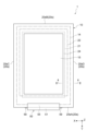
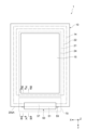
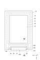
- FIG. 1 is a schematic plan view of an example power storage module.
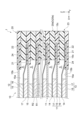
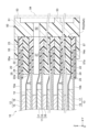
- FIG. 2 is a schematic cross-sectional view of an example power storage module.
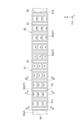
- FIG. 3 is a schematic front view of an example power storage module.
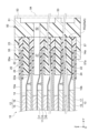
- FIG. 4 is a schematic cross-sectional view of an example power storage module.
- FIG. 5 is a schematic cross-sectional view of an example power storage module.
- FIG. 6 is a schematic cross-sectional view of an example power storage module.
- FIG. 7 is a flowchart illustrating an example of a method for manufacturing a power storage module.
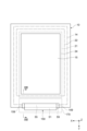
- FIG. 8 is a plan view showing the position of a mold attached to an example electricity storage module.
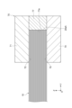
- FIG. 9 is a schematic cross-sectional view of an example mold.
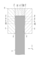
- FIG. 10 is a schematic cross-sectional view of an example mold.
- FIG. 1 is a schematic plan view of an example power storage module.
- FIG. 2 is a schematic cross-sectional view of an example power storage module.
- FIG. 3 is
- FIG. 11 is a schematic cross-sectional view of an example mold.
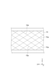
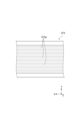
- FIG. 12 is a diagram showing the contact surface of the mold with respect to the electrode stack.
- FIG. 13 is a schematic plan view of another example of a power storage module.
- FIG. 14 is a schematic cross-sectional view of the power storage module shown in FIG. 13.
- FIG. 15 is a schematic cross-sectional view of the mold shown in FIG. 13.
- FIG. 16 is a schematic plan view of yet another example of a power storage module.
- FIG. 17 is a schematic cross-sectional view of the mold shown in FIG. 16.
- FIG. 18 is a schematic cross-sectional view of yet another example of a power storage module.
- FIG. 19 is a diagram showing another example of the contact surface of the mold with respect to the electrode stack.
- FIG. 1 is a schematic plan view of the electricity storage module according to the present embodiment.
- the power storage module 1 is, for example, a power storage module used in batteries of various vehicles such as forklifts, hybrid vehicles, and electric vehicles.
- the power storage module 1 is, for example, a secondary battery such as a nickel metal hydride secondary battery or a lithium ion secondary battery.
- the power storage module 1 may be an electric double layer capacitor or an all-solid-state battery. Here, a case is shown in which the power storage module 1 is a lithium ion secondary battery.
- the power storage module 1 includes an electrode laminate 10 and an injection resin part 50.
- the electrode stack 10 has a rectangular shape when viewed from the Z-axis direction (first direction).
- the electrode stack 10 has four outer surfaces 20s.
- the injection resin part 50 is joined to one outer surface 20sA (liquid injection port surface) of the four outer surfaces 20s.
- the outer surface 20sB is a surface opposite to the outer surface 20sA.
- the outer surface 20sC and the outer surface 20sD are surfaces that connect the outer surface 20sA and the outer surface 20sB.
- the power storage module may have a rectangular shape with a size of about 300 mm x 700 mm to 1300 mm x 2000 mm when viewed from the Z-axis direction.
- FIG. 2 is a cross-sectional view taken along line II-II in FIG. 1, showing the vicinity of the outer surface 20sD. Note that the cross section in the vicinity of the outer surfaces 20sB and 20sC is also similar to that in FIG. 2.
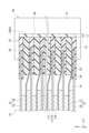
- FIG. 3 is a front view of the injection resin part 50, partially showing the outer surface 20sA. 4 is a cross section taken along line IV-IV in FIG. 3, FIG. 5 is a cross section taken along line VV in FIG. 3, and FIG. 6 is a cross section taken along line VI-VI in FIG. It is a cross section.
- the electrode stack 10 includes a plurality of electrodes stacked along the Z-axis direction.
- the Z-axis direction is the stacking direction of the electrodes and the height direction of the power storage module 1.
- the plurality of electrodes include a plurality of bipolar electrodes 11, a positive terminal electrode 12, and a negative terminal electrode 13.
- a separator 14 is interposed between adjacent electrodes.
- the bipolar electrode 11 has a current collector 15 , a positive electrode active material layer 16 , and a negative electrode active material layer 17 .
- the current collector 15 has a rectangular shape when viewed from the Z-axis direction, and has a sheet shape.
- the current collector 15 includes a first region R1 in which an active material layer (a positive electrode active material layer 16, a negative electrode active material layer 17) is formed, and a frame-shaped second region R2 that is outside the first region R1. has.
- the first region R1 is provided at the center of the current collector 15 when viewed from the Z-axis direction.
- the positive electrode active material layer 16 is provided on the first surface 15a of the current collector 15.
- the negative electrode active material layer 17 is provided on the second surface 15b of the current collector 15.
- the plurality of bipolar electrodes 11 are stacked such that the positive electrode active material layer 16 of one bipolar electrode 11 and the negative electrode active material layer 17 of the other bipolar electrode 11 adjacent to each other in the stacking direction face each other.
- the first surface 15a of the current collector 15 is a surface facing one direction in the Z-axis direction
- the second surface 15b of the current collector 15 is a surface facing the other direction in the Z-axis direction.
- the positive electrode active material layer 16 and the negative electrode active material layer 17 have a rectangular shape when viewed from the Z-axis direction.
- the negative electrode active material layer 17 is one size larger than the positive electrode active material layer 16 when viewed from the Z-axis direction. In plan view from the Z-axis direction, the entire formation region of the positive electrode active material layer 16 is located within the formation region of the negative electrode active material layer 17.
- the positive terminal electrode 12 includes a current collector 15 and a positive active material layer 16 provided on the first surface 15a of the current collector 15.
- the positive terminal electrode 12 does not have the positive active material layer 16 and the negative active material layer 17 on the second surface 15b of the current collector 15. That is, the active material layer is not provided on the second surface 15b of the current collector 15 of the positive terminal electrode 12.
- the positive terminal electrode 12 is stacked on the bipolar electrode 11 at the other end of the electrode stack 10 in the Z-axis direction.
- the positive terminal electrode 12 is stacked on the bipolar electrode 11 such that the positive active material layer 16 faces the negative active material layer 17 of the bipolar electrode 11 .
- the negative terminal electrode 13 includes a current collector 15 and a negative active material layer 17 provided on the second surface 15b of the current collector 15.
- the negative terminal electrode 13 does not have the positive active material layer 16 and the negative active material layer 17 on the first surface 15a of the current collector 15. That is, the first surface 15a of the current collector 15 of the negative terminal electrode 13 is not provided with an active material layer.
- the negative terminal electrode 13 is stacked on the bipolar electrode 11 at one end of the electrode stack 10 in the Z-axis direction.
- the negative terminal electrode 13 is stacked on the bipolar electrode 11 such that its negative active material layer 17 faces the positive active material layer 16 of the bipolar electrode 11 .
- the separators 14 are arranged between adjacent bipolar electrodes 11, between the positive terminal electrode 12 and the bipolar electrode 11, and between the negative terminal electrode 13 and the bipolar electrode 11.
- the separator 14 is interposed between the positive electrode active material layer 16 and the negative electrode active material layer 17, and isolates the positive electrode active material layer 16 and the negative electrode active material layer 17.
- the separator 14 allows charge carriers such as lithium ions to pass through while preventing short circuits due to contact between adjacent electrodes.
- the current collector 15 is a chemically inert electrical conductor that allows current to continue flowing through the positive electrode active material layer 16 and the negative electrode active material layer 17 during discharging or charging of the lithium ion secondary battery.
- the material of the current collector 15 is, for example, a metal material, a conductive resin material, or a conductive inorganic material.
- the conductive resin material include resins in which a conductive filler is added to a conductive polymer material or a non-conductive polymer material as necessary.
- Current collector 15 may include multiple layers. In this case, each layer of the current collector 15 may contain the above metal material or conductive resin material.
- a coating layer may be formed on the surface of the current collector 15.
- the coating layer may be formed by a known method such as plating or spray coating.
- the current collector 15 may have, for example, a plate shape, a foil shape (eg, metal foil), a film shape, or a mesh shape.
- the metal foil include aluminum foil, copper foil, nickel foil, titanium foil, and stainless steel foil.
- the stainless steel foil include SUS 304, SUS 316, and SUS 301 defined in JIS G 4305:2015. By using stainless steel foil as the current collector 15, the mechanical strength of the current collector 15 can be ensured.
- the current collector 15 may be an alloy foil or clad foil of the above metal. When the current collector 15 has a foil shape, the thickness of the current collector 15 may be, for example, 1 ⁇ m to 100 ⁇ m.
- the positive electrode active material layer 16 includes a positive electrode active material that can insert and release charge carriers such as lithium ions.
- the positive electrode active material include lithium composite metal oxides having a layered rock salt structure, metal oxides having a spinel structure, and polyanionic compounds.
- the positive electrode active material may be any material that can be used in lithium ion secondary batteries.
- the positive electrode active material layer 16 may include a plurality of positive electrode active materials.
- the positive electrode active material layer 16 contains olivine-type lithium iron phosphate (LiFePO 4 ) as a composite oxide.
- the negative electrode active material layer 17 includes a negative electrode active material that can insert and release charge carriers such as lithium ions.
- the negative electrode active material may be a single substance, an alloy, or a compound.
- Examples of the negative electrode active material include Li, carbon, and metal compounds.
- the negative electrode active material may be an element that can be alloyed with lithium, a compound thereof, or the like.
- Examples of carbon include natural graphite, artificial graphite, hard carbon (hardly graphitizable carbon), and soft carbon (easily graphitizable carbon).
- Examples of the artificial graphite include highly oriented graphite, mesocarbon microbeads, and the like.
- Examples of elements that can be alloyed with lithium include silicon, tin, and the like.
- the negative electrode active material layer 17 contains graphite as a carbon-based material.
- Each of the positive electrode active material layer 16 and the negative electrode active material layer 17 may contain a conductive agent, a binder, an electrolyte ( (a polymer matrix, an ion-conducting polymer, an electrolytic solution, etc.), an electrolyte supporting salt (lithium salt) for enhancing ion conductivity, and the like.
- the conductive additive is added to improve the conductivity of each electrode (bipolar electrode 11, positive terminal electrode 12, negative terminal electrode 13).
- the conductive aid include acetylene black, carbon black, and graphite.
- fluorine-containing resins such as polyvinylidene fluoride, polytetrafluoroethylene, and fluororubber, thermoplastic resins such as polypropylene and polyethylene, imide resins such as polyimide and polyamideimide, alkoxysilyl group-containing resins, and acrylic acid can be used.
- acrylic resins such as methacrylic acid, styrene-butadiene rubber (SBR), carboxymethyl cellulose, alginates such as sodium alginate and ammonium alginate, water-soluble cellulose ester crosslinked products, starch-acrylic acid graft polymers, and the like.
- SBR styrene-butadiene rubber
- alginates such as sodium alginate and ammonium alginate
- water-soluble cellulose ester crosslinked products starch-acrylic acid graft polymers, and the like.
- solvent for example, water, N-methyl-2-pyrrolidone (NMP), etc. are used.
- the separator 14 may be, for example, a porous sheet or nonwoven fabric containing a polymer that absorbs and retains electrolyte.
- Examples of the material for the separator 14 include polypropylene, polyethylene, polyolefin, polyester, and the like.
- Separator 14 may have a single layer structure or a multilayer structure.
- the multilayer structure may have, for example, a ceramic layer as an adhesive layer or a heat-resistant layer.
- the separator 14 may be impregnated with an electrolyte.
- the separator 14 may be made of an electrolyte such as a polymer electrolyte or an inorganic electrolyte.
- the electrolyte impregnated into the separator 14 is, for example, a liquid electrolyte (electrolyte) containing a non-aqueous solvent and an electrolyte salt dissolved in the non-aqueous solvent, or a polymer gel electrolyte containing an electrolyte held in a polymer matrix. etc.
- a liquid electrolyte electrolyte (electrolyte) containing a non-aqueous solvent and an electrolyte salt dissolved in the non-aqueous solvent
- a polymer gel electrolyte containing an electrolyte held in a polymer matrix.
- examples of the electrolyte salt include LiClO 4 , LiAsF 6 , LiPF 6 , LiBF 4 , LiCF 3 SO 3 , LiN(FSO 2 ) 2 , LiN(CF 3 SO 2 ) 2 and the like. Any known lithium salt may be used.
- nonaqueous solvent known solvents such as cyclic carbonates, cyclic esters, chain carbonates, chain esters, and ethers may be used. Note that two or more of these known solvent materials may be used in combination.
- the electrode stack 10 further includes a sealing body 20.
- the sealing body 20 is formed in a frame shape at the peripheral edge of the electrode stack 10 so as to form the outer edge of the electrode stack 10 when viewed from the Z-axis direction.
- the sealing body 20 can be joined to each of the first surface 15a and the second surface 15b of the current collector 15 at the peripheral edge 15c of each current collector 15.
- the sealing body 20 forms an internal space S between the current collectors 15 adjacent to each other in the Z-axis direction, and seals each of the internal spaces S.
- Each internal space S accommodates an electrolytic solution (not shown). That is, the sealing body 20 cooperates with the current collectors 15 adjacent to each other in the Z-axis direction to define an internal space S that accommodates the electrolyte.
- the sealing body 20 prevents the electrolyte from permeating to the outside.
- the sealing body 20 suppresses the intrusion of moisture and the like from the outside of the electrode stack 10 into the internal space S.
- the sealing body 20 prevents, for example, gas generated at each electrode due to a charging/discharging reaction or the like from leaking to the outside of the electricity storage module 1.
- the edge of the separator 14 is joined to the sealing body 20.
- the sealing body 20 includes an insulating material. Examples of the material of the sealing body 20 include various resin materials such as polypropylene, polyethylene, polystyrene, ABS resin, acid-modified polypropylene, acid-modified polyethylene, and acrylonitrile styrene resin.
- An example of the sealing body 20 includes a plurality of sealants 21 , a pair of end sealants 24 , and a plurality of spacers 22 .
- the sealing material 21, the end sealing material 24, and the spacer 22 may be frame-shaped members formed in a sheet shape. Further, the sealing body 20 is formed with a welded end portion 23 .
- the plurality of sealing materials 21 are provided in the second region R2 of the current collector 15 that constitutes the plurality of bipolar electrodes 11, respectively.
- the sealing material 21 has a frame shape when viewed from the Z-axis direction.
- the sealing material 21 is provided along the peripheral edge 15c of the current collector 15. Note that the peripheral edge portion 15c is the outer peripheral portion of the second region R2.
- the sealing material 21 is provided from the first surface 15a of the current collector 15 to the second surface 15b via the end surface, and covers the peripheral edge portion 15c.
- the sealing material 21 may be welded to at least one of the first surface 15a and the second surface 15b of the current collector 15.
- the end sealing material 24 is provided in the second region R2 of the current collector 15 that constitutes the positive end electrode 12 and the negative end electrode 13. Therefore, the end sealing materials 24 are arranged to sandwich the plurality of sealing materials 21 from the Z-axis direction.
- the end sealing material 24 has a frame shape when viewed from the Z-axis direction.
- the end sealing material 24 is provided along the peripheral edge 15c of the current collector 15. For example, when viewed from the Z direction, the width of the sealing material 21 in the region along the outer surface 20sA is wider than the width of the sealing material 21 in the region along the outer surfaces 20sB, 20sC, and 20sD. Further, the width of the end sealing material 24 is wider than the sealing material 21 when viewed from the Z-axis direction.
- the inner edge of the end sealing material 24 is located inside the inner edge of the sealing material 21.
- the width of the sealing material 21 in the region along the outer surfaces 20sA and 20sB may be the distance of the sealing material 21 in the region in the Y-axis direction (second direction).
- the width of the sealing material 21 in the region along the outer surfaces 20sC and 20sD may be the distance of the sealing material 21 in the region in the X-axis direction (third direction).
- the spacer 22 has a frame shape when viewed from the Z-axis direction.
- the spacer 22 is arranged along the peripheral edge 15c of the current collector 15.
- the spacer 22 is arranged to be interposed between the sealing materials 21 adjacent to each other in the Z-axis direction.
- the spacer 22 may be welded to at least one of the pair of sealing materials 21 adjacent to each other in the Z-axis direction.
- the spacer 22 is arranged to be interposed between the sealing material 21 and the end sealing material 24 that are adjacent to each other in the Z-axis direction.
- the spacer 22 may be welded to at least one of the sealing material 21 and the end sealing material 24 adjacent to each other in the Z-axis direction.
- the spacer 22 can maintain a space between the current collectors 15 adjacent to each other in the Z-axis direction. That is, the spacer 22, the sealing material 21, and the end sealing material 24 define an internal space S between adjacent current collectors 15.
- the width of the spacer 22 in the region along the outer surface 20sA is wider than the width of the spacer 22 in the region along the outer surfaces 20sB, 20sC, and 20sD. Further, in the regions along the outer surfaces 20sB, 20sC, and 20sD, the width of the spacer 22 is narrower than the width of the sealing material 21. That is, in the regions along the outer surfaces 20sB, 20sC, and 20sD, the inner edge of the spacer 22 is located outside the inner edge of the sealing material 21. On the other hand, in the region along the outer surface 20sA, the width of the spacer 22 is wider than the sealing material 21. That is, in the region along the outer surface 20sA, the inner edge of the spacer 22 is located inside the inner edge of the sealing material 21. Note that the inner edge of the spacer 22 is located outside the inner edge of the end sealing material 24 in any region.
- the welded end portion 23 is formed by welding and integrating ends of the plurality of sealing materials 21, the pair of end sealing materials 24, and the plurality of spacers 22 on the side opposite to the internal space S. ing.
- the welded end portion 23 surrounds the current collector 15 when viewed from the Z-axis direction, and has a frame shape so as to form the outer periphery of the electrode stack 10 .
- the side surface of the welded end portion 23 on the opposite side from the internal space S extends along the Z-axis direction and constitutes an outer surface 20s of the sealing body 20.
- the sealing body 20 includes an outer surface 20s opposite to the inner space S.
- the outer surface 20s may be formed as a flat surface.
- the sealing body 20 has a plurality of communication holes 27 that communicate with each of the plurality of internal spaces S (see FIG. 5).
- the communication hole 27 is a notch-shaped portion formed in the spacer 22.
- the communication hole 27 is formed to penetrate the welded end portion 23 .
- the communication hole 27 has one opening in the internal space S and the other opening in the outer surface 20s of the sealing body 20. In the illustrated example, an opening is formed in the outer surface 20sA.
- the injection resin part 50 is a reinforcing member that reinforces the outer surface 20sA in which the communication hole 27 is formed.
- the injection resin part 50 is molded into a predetermined shape to provide a liquid injection port communicating with the communication hole 27 .
- the injection resin part 50 is joined to the sealing body 20.
- the injection resin part 50 is integrally joined to the sealing body 20 by injection molding.
- An example of the injection resin part 50 includes a main body part 51 , a first overhang part 55 , a second overhang part 57 , and a first thin part 59 .
- the main body portion 51 partially covers the outer surface 20sA.
- the main body portion 51 covers the outer surface 20sA so as to include a region (main body region) R3 in which the plurality of communicating holes 27 are formed.
- the plurality of communication holes 27 communicate with the plurality of internal spaces S, respectively.
- 30 communication holes 27 corresponding to the 30 layers of internal space formed between the respective current collectors 15 are arranged discretely in the X-axis direction and the Z-axis direction.
- communication holes 27 corresponding to the internal spaces of the first to tenth layers are arranged with the positive terminal electrode 12 side as the base end, and are arranged at equal intervals along the X-axis direction, and the 11th layer
- the communication holes 27 corresponding to the internal spaces from the 1st to 20th layers and the communication holes 27 corresponding to the internal spaces from the 21st to 30th layers are located below the internal spaces from the 1st to 10th layers. are arranged in order in the Z-axis direction.
- the main body portion 51 extends in a rectangular shape along the X-axis direction and the Z-axis direction in order to cover the main body region R3 in which these 30 communication holes 27 are formed.
- the main body portion 51 is formed into a rectangular plate shape with a predetermined thickness in the Y-axis direction.
- the thickness L2 of the main body portion 51 in the Y-axis direction may be 2.0 ⁇ 0.5 mm.
- the main body portion 51 has an opening 52 at a position corresponding to the communication hole 27 .
- the thickness L2 of the main body 51 corresponds to the depth of the opening 52 provided in the main body 51 in the Y-axis direction.
- the main body portion 51 has a frame-shaped protruding frame portion 53 that protrudes outward along the Y-axis direction.
- the protruding frame portion 53 surrounds each opening 52 when viewed from the Y-axis direction (see FIG.
- protruding frame portion 53 is arranged in the X-axis direction in which three spaces are formed to separate three vertically arranged openings 52.
- the thickness of the protruding frame portion 53 in the Y-axis direction may be approximately 0.5 mm to 6.0 mm.
- the protruding frame portion 53 is used, for example, when pouring electrolyte into each of the internal spaces S.
- the nozzle of the injector is brought into close contact with the top surface of the protruding frame 53, and the electrolyte is introduced from the nozzle into the space of each protruding frame 53. . Thereby, it becomes possible to inject the electrolytic solution into the internal space S from the opening 52 and the communication hole 27.
- a laminate sheet 54 for sealing the protruding frame portion 53 may be provided on the protruding frame portion 53 (see FIG. 5).
- the laminate sheet 54 may be, for example, a sheet in which a metal layer such as aluminum is coated with a resin layer.
- the laminate sheet 54 may be fused to the top surface of the protruding frame portion 53, for example.
- both end faces of the electrode stack 10 in the Z-axis direction are constituted by a first end face 10a and a second end face 10b.
- the first end surface 10a is the outermost surface of the electrode stack 10 on the positive side in the Z-axis direction. That is, the first end surface 10a includes the exposed surface of the second surface 15b of the positive terminal electrode 12 and the exposed surface of the end sealing material 24 joined to the periphery of the positive terminal electrode 12.
- the second end surface 10b is the outermost surface of the electrode stack 10 on the negative side in the Z-axis direction.
- the second end surface 10b includes the exposed surface of the first surface 15a of the negative terminal electrode 13 and the exposed surface of the end sealing material 24 joined to the periphery of the negative terminal electrode 13.
- the first overhang portion 55 is connected to the first end edge 51a of the main body portion 51 in the Z-axis direction.
- the first overhang portion 55 partially covers the first end surface 10a of the electrode stack 10.
- the first overhang portion 55 partially covers the end sealing material 24 joined to the positive terminal electrode 12 forming the first end surface 10a.
- the end edge 55a of the first overhang portion 55 extends to a position inside the outer edge 14a of the separator 14 and outside the inner edge 22a of the spacer 22 when viewed from the Z-axis direction. are doing.
- the first overhang portion 55 may be formed into a rectangular plate shape having the same length as the main body portion 51 in the X-axis direction.
- the thickness of the first overhang portion 55 in the Z-axis direction may be 1.5 ⁇ 0.5 mm or may be thinner.
- the second overhang portion 57 is connected to a second edge 51b of the main body portion 51 opposite to the first edge 51a, and partially covers the second end surface 10b of the electrode stack 10.
- the second overhang portion 57 partially covers the end sealing material 24 joined to the negative terminal electrode 13 forming the second end surface 10b.
- the end edge 57a of the second overhang portion 57 extends to a position inside the outer edge 14a of the separator 14 and outside the inner edge 22a of the spacer 22 when viewed from the Z-axis direction. are doing.
- the second overhang portion 57 may be formed into a rectangular plate shape having the same length as the main body portion 51 in the X-axis direction.
- the thickness of the second overhang portion 57 in the Z-axis direction may be 1.5 ⁇ 0.5 mm, and may be different from the thickness of the first overhang portion 55.
- the first thin portion 59 is formed so as to be connected to a third end edge 51c and a fourth end edge 51d, which are both ends of the main body portion 51 in the X-axis direction (see FIG. 3).
- the first thin portion 59 extends from the main body portion 51 along the outer surface 20sA, and is joined to the outer surface 20sA.
- the size of the first thin portion 59 in the Z-axis direction may be the same as the size of the main body portion 51 in the Z-axis direction.
- the thickness L1 of the first thin portion 59 in the Y-axis direction (see FIG. 6) is smaller than the thickness L2 of the main body portion 51 in the Y-axis direction (see FIG. 4).
- the thickness L1 of the first thin portion 59 may be 1/3 or less of the thickness L2 of the main body portion 51.
- the thickness of the first thin portion 59 in the Y-axis direction may be 0.5 mm or less.
- the first thin part 59 has a rectangular shape when viewed from the Y-axis direction, but if the first thin part 59 has a region that joins to the outer surface 20sA, The shape of the first thin portion 59 is often not limited to a rectangular shape.
- a current is applied from the electricity storage module 1 to the first surface 15a of the current collector 15 of the positive terminal electrode 12 and the second surface 15b of the current collector 15 of the negative terminal electrode 13 exposed from the sealing body 20.
- a conductive member functioning as a terminal for taking out may be arranged and electrically connected.
- the conductive member can be used to electrically connect the plurality of power storage modules 1.
- the conductive member can also be used as a restraining member to apply a restraining load to the electrode stack 10.
- a cooling channel may be formed in the conductive member.
- the electrode stack 10 can be cooled by flowing a cooling medium through a cooling channel formed in the conductive member.
- FIG. 7 is a flow diagram illustrating an example of a method for manufacturing a power storage module.
- an electrode stack 10 including a plurality of electrodes stacked along the Z-axis direction is formed (step S1).
- the electrode stack 10 is prepared.
- the sealing body 20 of the electrode stack 10 that is formed does not have the welded end portion 23. That is, the end sealing material 24, the sealing material 21, and the spacer 22, which are stacked along the Z-axis direction, are not welded to each other.
- the spacer 22 may have a notch-shaped portion connected from the internal space S to the outer edge at a position corresponding to the communication hole 27.
- the electrode stack 10 is formed with a nest placed in a notch-shaped portion formed in the spacer 22.
- the electrode stack 10 formed in this manner has a plurality of nests protruding from the side surface corresponding to the outer surface 20sA. By being inserted into the notch-like portion, the nest prevents the notch-like portion from being blocked in subsequent steps. By removing the insert after injection molding, the communicating hole 27 and the opening 52 are formed in the portion where the insert is placed.
- the nest may be a metal plate, for example.
- welded end portions 23 are formed on the electrode stack 10 (step S2). Thereby, an internal space S is formed between adjacent current collectors 15.
- the outer edge portions of the sealing material 21, the end sealing material 24, and the spacer 22, which constitute the electrode stack 10, on the side opposite to the internal space S are welded to each other.
- the welded end portion 23 is formed with the nest placed in the cutout portion of the spacer 22 .
- the thickness of the welded end 23 corresponding to the other outer surfaces 20sB, 20sC, and 20sD may be thicker than the thickness of the welded end 23 corresponding to the outer surface 20sA.
- FIG. 8 is a plan view showing the position of a mold 70 attached to an example of an electricity storage module. In FIG. 8, the mounting position of the mold 70 is indicated by a broken line.
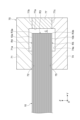
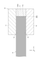
- FIG. 9 is a cross-sectional view schematically showing the mold at the position taken along line IX-IX in FIG.
- FIG. 10 is a cross-sectional view schematically showing the mold at the line XX in FIG.
- FIG. 11 is a cross-sectional view schematically showing the mold at the position of line XI-XI in FIG. 8.
- step S3 the mold 70 is attached to the electrode stack 10 placed on the mounting table, thereby forming a main body region R3, a first overhang region R4, and a second overhang region R5 of the electrode stack 10.
- a continuous molding space C is formed between them (see FIG. 9).
- the thickness of the molding space C in the Y-axis direction corresponds to the thickness L2 of the main body portion 51 (see FIG. 4). Further, the thickness of the molding space C in the Z-axis direction may be controlled to be constant. Thereby, the electricity storage module 1 can be manufactured accurately and stably. If there is a tolerance in the size of the electrode stack 10, the volume of the molding space C may vary, for example, depending on the thickness of the electrode stack 10 placed in the mold 70 in the Z-axis direction. In this case, the first overhang portion 55 and the second overhang portion 57 may have different thicknesses.
- the main body region R3 is a region of the outer surface 20sA that includes a plurality of communication holes 27.
- the main body region R3 is a joint surface with the main body part 51.
- the first overhang region R4 is connected to the first end edge R3a of the main body region R3 in the Z-axis direction.
- the first overhang region R4 is a region that partially extends to the first end surface 10a of the electrode stack 10 that intersects with the Z-axis direction.
- the first overhang region R4 is a joint surface with the first overhang portion 55.
- the second overhang region R5 is connected to a second edge R3b of the main body region R3 on the opposite side to the first edge R3a.
- the second overhang region R5 is a region that partially extends to the second end surface 10b of the electrode stack 10 on the opposite side to the first end surface 10a.
- the second overhang region R5 is a joint surface with the second overhang portion 57.
- a first thin space SS1 extending from the molding space C along the outer surface 20sA is formed (see FIG. 10).
- the thickness of the first thin space SS1 in the Y-axis direction corresponds to the thickness L1 of the first thin portion 59 (see FIG. 4).
- the first thin space SS1 is a space formed in the mold 70 together with the molding space C, so it can be considered as a part of the molding space C, but in this specification, the first thin space SS1
- the thin space SS1 is defined as another space connected to the molding space C.
- the mold 70 may include a first mold 71 and a second mold 74 that sandwich the electrode stack 10 from the Z-axis direction. Furthermore, the mold 70 may include a third mold 77 disposed between the first mold 71 and the second mold 74. As shown in FIG. 9, the first mold 71 has a contact surface 72 that contacts the first end surface 10a of the electrode stack 10, and an inner surface 71a that faces the first overhang region R4. Similarly, the second mold 74 has a contact surface 75 that contacts the second end surface 10b of the electrode stack 10, and an inner surface 74a that faces the second overhang region R5.
- the contact surface 72 of the first mold 71 and the second mold 74 are brought into contact so that the outer edge of the electrode stack 10 is exposed in the molding space C.
- the electrode stack 10 is held between the surfaces 75 .
- the contact surface 72 of the first mold 71 may contact the end sealing material 24 at a position where the spacer 22, the sealing material 21, and the separator 14 overlap when viewed from the Z-axis direction.
- the contact surface 75 of the second mold 74 may contact the end sealing material 24 at a position where the spacer 22, the sealing material 21, and the separator 14 overlap.
- the current collector 15 may extend at a position where the spacer 22, the sealing material 21, and the separator 14 overlap.
- the third mold 77 is arranged between the first mold 71 and the second mold 74 in the Z-axis direction, and forms a molding space C together with the first mold 71 and the second mold 74.
- the third mold 77 includes a contact surface 77b that contacts the first mold 71, a contact surface 77c that contacts the second mold 74, and an inner surface 77a that faces the main body region R3.
- the inner surface 77a of the third mold 77 extends a distance corresponding to the thickness L2 of the main body part 51 (see FIG. 4) from the main body region R3 of the outer surface 20sA. They are separated.
- the second mold 74 is first placed in contact with the electrode stack 10.
- the electrode stack 10 may be placed on the mounting table so that the end portion including the outer surface 20sA protrudes from the mounting table.
- the first mold 71 presses the electrode stack 10 from the Z-axis direction, so that the electrode stack 10 is sandwiched between the first mold 71 and the second mold 74.
- the third mold 77 is placed.
- the mold 70 only needs to partially cover the outer surface 20sA of the electrode stack 10. In one example, both ends of the outer surface 20sA in the X-axis direction may be exposed to the outside of the mold 70.
- the contact surface 72 of the first mold 71 and the area outside the area where the main body part 51 is formed and where the first thin part 59 is formed are The contact surfaces 75 of the two molds 74 extend to a position of the outer surface 20sA, which is the outer periphery of the electrode stack 10.
- the third mold 77 has an inner surface 77d that is closer to the outer surface 20sA of the electrode stack 10 than the inner surface 77a.
- the inner surface 77d faces the first thin region R6 to which the first thin portion 59 is joined on the outer surface 20sA.
- the distance from the inner surface 77d to the outer surface 20sA corresponds to the thickness L1 of the first thin portion 59 (see FIG. 6).
- the contact surfaces of the first mold 71 and the second mold 74 are similar to the area where the first thin part 59 is formed, and the electrode stack 10 is It extends to a position of 20 sA on the outer surface of.
- the third mold 77 has a contact surface 77e that contacts the outer surface 20sA. In a state where the mold 70 is attached to the electrode stack 10, the contact surface 77e of the third mold 77 may be pressed against the outer surface 20sA of the electrode stack 10.
- FIG. 12 is a diagram schematically showing the contact surface of the mold with respect to the electrode stack.
- the contact surface 72 of the first mold 71 and the contact surface 75 of the second mold 74 have the same shape.
- the contact surface 72 of the first mold 71 is shown as a representative.
- a groove is formed in the contact surface 72 of the first mold 71.
- the illustrated grooves form a mesh pattern when viewed from the Z-axis direction. That is, the groove is formed by a plurality of first straight lines 72a inclined at a first angle and a plurality of second straight lines 72b inclined at a second angle intersecting each other when viewed from the Z-axis direction. There is.
- the first straight line 72a and the second straight line 72b both intersect both the X-axis direction and the Y-axis direction.
- the surface roughness of the contact surfaces of the first mold 71 and the second mold 74 is greater than the surface roughness of the forming surface (i.e., the inner surface) of the molding space C in the mold 70.
- both ends of the contact surface 72 in the Y-axis direction may be rounded.
- the injection resin part 50 is molded by injecting resin into the molding space C of the mold 70 (step S4).
- the molding space C is filled with resin, and the resin leaked from the molding space C can be filled into the first thin space SS1.
- the first thin space SS1 does not necessarily need to be completely filled with the resin, and it is sufficient that the resin enters even partially. That is, the first thin portion 59 formed in step S4 does not need to have a rectangular shape corresponding to the first thin space SS1 when viewed from the Y-axis direction, and may have a chip at the end or the periphery. Good too.
- the mold 70 may have a recess or the like corresponding to the protruding frame portion 53. Further, for example, the mold 70 may be formed with a holding portion that holds the nest protruding from the electrode stack 10. After the injection resin part 50 is formed in step S4, by pulling out the nest, an opening 52 connected to the communication hole 27 is formed in the injection resin part 50 joined to the electrode stack 10.
- FIG. 13 is a schematic plan view of another example of a power storage module.
- FIG. 14 is a schematic cross-sectional view of the power storage module shown in FIG. 13.
- FIG. 15 is a schematic cross-sectional view of the mold shown in FIG. 13.
- the power storage module has an injected resin portion 150 having a shape different from that of the injected resin portion 50.
- the injection resin part 150 includes a main body part 51 , a first overhang part 55 , a second overhang part 57 , a first thin part 59 , and a second thin part 159 .
- the main body part 51, the first overhang part 55, the second overhang part 57, and the first thin part 59 have the same configuration as the injection resin part 50, so the description thereof will be omitted.
- the second thin portions 159 are connected to both ends of the first overhang portion 55 and the second overhang portion 57 in the X-axis direction. Further, the second thin portion 159 may be connected to the first thin portion 59. The second thin portion 159 extends from the first overhang portion 55 and the second overhang portion 57 along the end sealing material 24, respectively.
- the thickness L3 of the second thin portion 159 in the Z-axis direction is smaller than the thicknesses L4 and L5 of the first overhang portion 55 and the second overhang portion 57 in the Z-axis direction. For example, the thickness L3 may be 1/3 or less of the thickness L4 or the thickness L5.
- the second thin portion 159 and the first thin portion 59 may have the same thickness, and the thickness L3 of the second thin portion 159 and the thickness of the first overhang portion 55 and the second overhang portion 57 may be the same.
- the relationship between L4 and L5 may be the same as the relationship between the thickness L1 of the first thin portion 59 and the thickness L2 of the main body portion 51.
- the second thin portion 159 has a rectangular shape when viewed from the Z-axis direction, but the shape of the second thin portion 159 is not limited to the rectangular shape.
- FIG. 15 is a cross-sectional view of the mold 170 at a position corresponding to the second thin part 159, the first mold 171, the second mold 174, and the third mold 177 that constitute the mold 170.
- a first thin space SS1 and a second thin space SS2 for forming the first thin part 59 and the second thin part 159 are formed.
- the first mold 171 has a contact surface 172 that contacts the first end surface 10a (end sealing material 24) of the electrode stack 10 in the range where the second thin part 159 is formed in the X-axis direction;
- the first end surface 10a has an inner surface 171a facing the second thin region R7, which is a region to which the second thin portion 159 is joined.
- the second mold 174 has a contact surface 175 that contacts the second end surface 10b (end seal material 24) of the electrode stack 10 in the range where the second thin wall portion 159 is formed in the X-axis direction. , and has an inner surface 174a facing the second thin region R7, which is a region to which the second thin portion 159 is joined on the second end surface 10b.
- the inner surface 171a of the first mold 171 and the inner surface 174a of the second mold 174 are spaced apart from the electrode stack 10 by a distance corresponding to the second thin portion 159.
- the third mold 177 includes a contact surface 177a that contacts the first mold 171, a contact surface 177b that contacts the second mold 174, and an inner surface 177c that faces the outer surface 20sA.
- the inner surface 177c of the third mold 177 is spaced apart from the outer surface 20sA by a distance corresponding to the first thin part 59.
- the resin filled in the molding space C of the mold 170 is distributed to the first thin space SS1 and the second thin wall space SS1. It flows into space SS2. As a result, the first thin portion 59 and the second thin portion 159 are formed.
- FIG. 16 is a schematic plan view of yet another example of a power storage module.
- FIG. 17 is a schematic cross-sectional view of the mold shown in FIG. 16.
- the power storage module has an injected resin portion 250 having a shape different from that of the injected resin portion 150.
- the injection resin part 250 includes a main body part 51 , a first overhang part 55 , a second overhang part 57 , a first thin part 59 , a second thin part 159 , and a third thin part 259 .
- the main body part 51, the first overhang part 55, the second overhang part 57, the first thin part 59, and the second thin part 159 have the same configuration as the injection resin part 150, so a description thereof will be omitted.
- the third thin portion 259 is connected to the edges of the first overhang portion 55 and the second overhang portion 57 in the Y-axis direction. Further, the third thin portion 259 may be connected to the second thin portion 159. The third thin portion 259 extends from the first overhang portion 55 and the second overhang portion 57 along the end sealing material 24, respectively.
- the thickness of the third thin portion 259 in the Z-axis direction is smaller than the thickness of the first overhang portion 55 and the second overhang portion 57 in the Z-axis direction, and is, for example, the same as the thickness of the second thin portion 159. good.
- the third thin portion 259 has a rectangular shape when viewed from the Z-axis direction, but the shape of the third thin portion 259 is not limited to the rectangular shape.
- the first mold 271 has an electrode lamination layer in the range where the third thin part 259 is formed in the X-axis direction.
- a contact surface 272 that contacts the first end surface 10a (end seal material 24) of the body 10, and an inner surface 271a that faces the third thin region R8, which is the region where the third thin portion 259 is joined on the first end surface 10a. and an inner surface 271b facing the first overhang region R4.
- the second mold 274 has a contact surface 275 that contacts the second end surface 10b (end seal material 24) of the electrode stack 10 in the range where the third thin wall portion 259 is formed in the X-axis direction. , has an inner surface 274a facing the third thin region R8, which is a region to which the third thin portion 259 is joined on the first end surface 10a, and an inner surface 274b facing the second overhang region R5.
- the inner surface 271a of the first mold 271 and the inner surface 274a of the second mold 274 are spaced apart from the electrode stack 10 (end sealing material 24) by a distance corresponding to the third thin portion 259.
- the third mold 277 includes a contact surface 277b that contacts the first mold 271, a contact surface 277c that contacts the second mold 274, and an inner surface 277a that faces the main body region R3.
- the resin filled in the molding space C of the mold 270 is distributed to the first thin space SS1 and the second thin wall space SS1. It flows into the space SS2 and the third thin space SS3. As a result, the first thin portion 59, the second thin portion 159, and the third thin portion 259 are formed.
- FIG. 18 is a schematic cross-sectional view of yet another example of a power storage module.
- the power storage module has the injection resin part 50 like the example of FIG. 5, but the power storage module may have the injection resin part 150 or the injection resin part 250.
- a laminate sheet 25 may be joined to the end sealing material 24 that constitutes the first end surface 10a and the second end surface 10b of the electrode stack 10.
- the laminate sheet 25 may be welded to the end sealing material 24.
- the laminate sheet 25 may be a sheet in which a metal layer such as aluminum is covered with a resin layer.
- the end sealing material 24 may be covered with a laminate sheet 25.
- a surface along the first end surface 10a of the end sealing material 24 joined to the positive terminal electrode 12 and a surface along the second end surface 10b of the end sealing material 24 joined to the negative terminal electrode 13 are shown.
- the shape of the laminate sheet 25 matches the shape of the end sealing material 24 when viewed from the Z-axis direction.
- the laminate sheet 25 may be joined to the end sealing material 24 at any stage before step S3 described above. By bonding the laminate sheet 25 to the outer surface of the end sealing material 24, the rigidity of the electrode laminate 10 is improved. Thereby, the mold can be more stably attached to the electrode stack 10, for example in step S3.
- FIG. 19 is a diagram showing another example of the contact surface of the mold with respect to the electrode stack.
- a groove is formed in the abutment surface 372 of the mold shown in FIG.
- a plurality of grooves 372a extending in the X-axis direction when viewed from the Z-axis direction are formed in the abutment surface 372 in the illustrated example.
- the respective grooves 372a are equally spaced apart in the Y-axis direction.
- the electricity storage module 1 as an example includes a plurality of electrodes (bipolar electrode 11, positive terminal electrode 12, negative terminal electrode 13) stacked along the first direction, and there is a gap between adjacent electrodes.
- the electrode stack 10 includes a sealing body 20 that forms an internal space S and is provided to seal the internal space S, and an injection resin part 50 joined to the sealing body 20.
- Each of the plurality of electrodes includes a current collector 15 having a rectangular shape when viewed from the Z-axis direction.
- the sealing body 20 is a welded end in which the outer peripheral edges of a plurality of frame-like members (sealing material 21, spacer 22) interposed between a plurality of current collectors 15 and stacked in the Z-axis direction are welded to each other. 23.
- the sealing body 20 includes a first end surface 10a and a second end surface 10b, which are both end surfaces of the electrode stack 10 in the Z-axis direction, and a peripheral surface of the welded end portion 23 (defining an outer edge when viewed from the Z-axis direction).
- the outer surface 20sA which is one of the four outer surfaces 20s constituting the outer surface 20s and to which the injection resin part 50 is joined, communicates with the outside of the outer surface 20sA and each of the plurality of internal spaces S. It has a plurality of communication holes 27.
- the injection resin part 50 has a plurality of openings 52 each connected to a plurality of communication holes 27, and a main body part 51 that partially covers the outer surface 20sA, and a main body part 51 that is connected to the main body part 51 and has a first end surface 10a. It includes a first overhang part 55 that partially covers the main body part 51 and a second overhang part 57 that is connected to the main body part 51 and partially covers the second end surface 10b.
- the main body portion 51 includes a plurality of protruding frame portions 53 that protrude in the Y-axis direction intersecting the outer surface 20sA.
- the plurality of protruding frame parts 53 surround the openings 52 connected to each of the plurality of communication holes 27 when viewed from the Y-axis direction.
- a communication hole 27 penetrating to the internal space S is provided in the welded end portion 23 of the sealing body 20 formed on the outer peripheral edge of the electrode stack 10.
- An injection resin part 50 having a protruding frame part 53 surrounding the communication hole 27 is bonded to the sealing body 20 .
- This injection resin part 50 includes a main body part 51 that covers the outer surface 20sA on which the welded end part 23 is formed, and a first overhang part 55 that extends from the main body part 51 to the first end surface 10a of the electrode stack 10. , and a second overhang portion 57 extending from the main body portion 51 to the second end surface 10b of the electrode stack 10.
- the injection resin part 50 is provided on only one of the four outer surfaces, the size of the power storage module 1 is suppressed from increasing.
- Such an injection resin part 50 does not require a mold large enough to surround the entire circumference of the electrode stack 10, but can be formed using a mold large enough to partially cover one outer surface 20sA of the electrode stack 10. It is possible. Therefore, it is possible to suppress the size of the mold required for manufacturing from increasing. Further, by providing the first overhang part 55 and the second overhang part 57, the injection resin part 50 can be firmly joined to the sealing body 20, and the Z-axis between the internal space S and the outside can be Moisture permeation along the direction is suppressed and gas permeation is suppressed.
- the outer surface 20s of the electrode stack 10 is formed by welding a sealing material 21, an end sealing material 24, and a spacer 22. Therefore, the outer surface 20s is not necessarily a flat surface, but may be formed by an uneven end surface. When the outer surface 20s has irregularities, it is conceivable that the bondability between the outer surface 20s and the injection resin part 50 is reduced.
- the injection resin part 50 as an example may include a first thin part 59 that is connected to the main body part 51 and joined to the outer surface 20sA from the main body part 51 along the outer surface 20sA.
- the thickness of the main body portion 59 in the Y-axis direction is smaller than the thickness of the main body portion 51 in the Y-axis direction.
- An example of the injection resin part 150 may include a second thin part 159 connected to the first overhang part 55 and joined to the first end face 10a from the first overhang part 55 along the first end face 10a.
- the thickness of the second thin portion 159 in the Z-axis direction is often smaller than the thickness of the first overhang portion 55 in the Z-axis direction.
- the injection resin part 250 as an example has a third thin part 259 connected to the first overhang part 55 and joined to the first end face 10a from the first overhang part 55 along the first end face 10a.
- the thickness of the third thin portion 259 in the Z-axis direction is smaller than the thickness of the first overhang portion 55 in the Z-axis direction.
- An example of the current collector 15 includes a first region R1 provided at the center of the current collector 15 when viewed from the Z-axis direction and in which an active material layer is formed, and a frame-shaped region outside the first region R1. It has a second region R2.
- the electrode stack 10 is interposed between a plurality of frame-shaped sealing materials 21 provided in the second region R2 of each of the plurality of current collectors 15 and the sealing materials 21 adjacent to each other in the Z-axis direction. It may also include a plurality of spacers 22 that define an internal space S between the current collectors 15 together with the sealing material 21 . In this configuration, the outer circumferential edge of the sealing material 21 and the outer circumferential edge of the spacer 22 are welded to each other, thereby forming the welded end portion 23.
- an example method for manufacturing the power storage module 1 includes an electrode stack 10 including a plurality of electrodes stacked along the Z-axis direction, and having both end faces in the Z-axis direction as a first end face 10a and a second end face 10b.
- a step of preparing (step S1), a step of providing the welded end portions 23 on the electrode stack 10 so that an internal space S is formed between adjacent electrodes (step S2), and injection into the welded end portions 23.
- a step of forming the resin portion 50 (step S3) is provided.
- the step of providing the welded end portions 23 includes the step of welding the outer peripheral edges of the plurality of sealing materials 21, the plurality of spacers 22, and the end sealing materials 24 to each other.
- the step of forming the injection resin part 50 includes forming a main body region R3 including a plurality of communication holes 27 in the outer surface 20sA, and a first overhang region connected to the main body region R3 and partially extending to the first end surface 10a.
- a mold is formed in the electrode stack 10 so that a continuous molding space C is formed between R4 and a second overhang region R5 that connects to the main body region R3 and partially extends to the second end surface 10b. 70; and a step of molding the injection resin part 50 by injecting resin into the molding space C attached to the electrode stack 10.
- the method for manufacturing the electricity storage module 1 described above does not require a mold sized to surround the entire circumference of the electrode laminate 10, but a mold 70 sized to partially cover one outer surface 20sA of the electrode laminate 10 is used.
- An injection resin part 50 can be formed. Therefore, it is possible to suppress the size of the mold required for manufacturing from increasing. Further, the size of the manufactured electricity storage module is suppressed from increasing. Moreover, if the shape of the injection resin part 50 is the same, a common mold can be used even if the electrode stack has a larger electrode.
- the step of attaching the mold 70 may connect to the molding space C and form a first thin space SS1 extending from the molding space C along the outer surface 20sA, and the first thin space SS1 may be connected to the molding space C and extending from the molding space C along the outer surface 20sA.
- the thickness in the Y-axis direction is smaller than the thickness of the molding space C in the Y-axis direction.
- the step of attaching the mold may include forming a second thin space SS2 connected to the molding space C and extending from the first overhang region R4 along the first end surface 10a;
- the thickness of the space SS2 in the Z-axis direction is smaller than the thickness of the molding space C in the first overhang region R4 in the Z-axis direction.
- the step of attaching a mold includes an electrode stack 10 in which a plurality of current collectors 15, a plurality of sealants 21, a plurality of spacers 22, and a plurality of separators 14 overlap when viewed from the Z-axis direction.
- the area may be held between the molds 70.
- the electrode stack 10 can be stably held between the molds 70.
- An example mold 70 includes a first mold 71 and a second mold 74 that sandwich the electrode stack 10 from the Z-axis direction, and includes a contact surface 72 that contacts the electrode stack 10 in the first mold 71 and a second mold 74 that holds the electrode stack 10 between them.
- the surface roughness of the contact surface 75 of the second mold 74 that contacts the electrode stack 10 may be greater than the surface roughness of the surface of the mold 70 on which the molding space C is formed.
- the welded end portion 23 is formed outside the edge of the current collector 15, the welded end portion 23 may be formed along the edge of the current collector 15, or may be formed along the edge of the current collector 15. It may be formed to the inside of the edge of the electric body 15.
- the shape of the active material layer is not particularly limited as long as it can be regarded as rectangular.
- the active material layer may be divided into a plurality of regions spaced apart from each other, or may have a shape other than a rectangle.
- the shape of the active material layer is such that the long side of the smallest rectangle that includes all the regions in which the active material layer is formed is along the long side of the current collector, and It may be considered to be a rectangle with the short sides along the short sides.
- the first thin portions are formed at both ends of the main body portion 51 in the X-axis direction
- the first thin portions are formed only at one end of the main body portion 51 in the X-axis direction. It's okay.
- the first thin part is formed over the entire area in the Z-axis direction at the end of the main body part 51 in the X-axis direction
- the first thin part is formed only in a part of the X-axis direction. It's okay. That is, the size of the first thin portion in the Z-axis direction may be smaller than the size of the main body portion in the Z-axis direction.
- the spacer 22 is illustrated in which both the outer edge and the inner edge are rectangular, the planar shape of the spacer 22 is not limited to this.
- the width of the spacer 22 is larger than the width of the sealing material 21 in the range where the mold is provided in the X-axis direction, and the width of the spacer 22 is larger than the width of the sealant 21 in the region where the mold is provided in the X-axis direction.
- the width of the area may be smaller than the width of the sealing material 21. That is, in the region along the outer surface 20sA, the inner edge of the spacer 22 is located inside the inner edge of the sealing material 21 in the range where the mold is provided, and is located outside the inner edge of the sealing material 21 in other regions. may be located.
- the thickness L2 of the main body portion 51 in the Y-axis direction is 2.0 ⁇ 0.5 mm
- the thickness L2 of the main body portion 51 may be larger or smaller.
- the thickness of the protruding frame portion 53 in the Y-axis direction is approximately 0.5 mm to 6.0 mm
- the thickness of the protruding frame portion 53 is not limited to this.
- the thickness L1 of the first thin part 59 is 1/3 or less of the thickness L2 of the main body part 51
- the thickness L1 of the first thin part 59 is not limited to this, and for example, It may be about 1/2 of the thickness L2 of the main body portion 51.
- 0.5 mm was illustrated as a specific example of the thickness L1 of the 1st thin part 59, the thickness L1 is not limited to this.
- SYMBOLS 1 Electricity storage module, 10... Electrode laminated body, 11... Bipolar electrode (electrode), 12... Positive electrode terminal electrode (electrode), 13... Negative electrode terminal electrode (electrode), 15... Current collector, 20... Sealing body, 20sA ...Outer surface (liquid inlet surface), 21...Sealing material (frame-shaped member), 22...Spacer (frame-shaped member), 24...End sealing material (sealing material, frame-shaped member), 27...Communication hole, 50 , 150, 250... Injection resin part, 51... Main body part, 53... Projection frame part, 55... First overhang part, 57... Second overhang part.
Landscapes
- Engineering & Computer Science (AREA)
- Power Engineering (AREA)
- Chemical & Material Sciences (AREA)
- Chemical Kinetics & Catalysis (AREA)
- Electrochemistry (AREA)
- General Chemical & Material Sciences (AREA)
- Microelectronics & Electronic Packaging (AREA)
- Manufacturing & Machinery (AREA)
- Sealing Battery Cases Or Jackets (AREA)
- Secondary Cells (AREA)
- Electric Double-Layer Capacitors Or The Like (AREA)
- Filling, Topping-Up Batteries (AREA)
Abstract
Description
Claims (9)
- 第1方向に沿って積層された複数の電極を含む電極積層体であって、隣り合う前記電極同士の間に内部空間を形成するとともに、当該内部空間を封止するように設けられた封止体を含む前記電極積層体と、
前記封止体に接合された射出樹脂部と、を備え、
前記複数の電極は、前記第1方向から見て矩形状をなす複数の集電体を含み、
前記封止体は、
前記第1方向に隣り合う前記集電体同士の間に介在して前記第1方向に積層された複数の枠状部材の外周縁同士が互いに溶着された溶着端部であって、前記第1方向から見て前記複数の集電体を囲み、前記第1方向に沿って延在する4つの外側面を有する前記溶着端部を含んでおり、
前記電極積層体の前記第1方向における両端面である第1端面及び第2端面と、
前記4つの外側面のうちの一つであって前記射出樹脂部が接合された注液口面と、
前記注液口面の外側と複数の前記内部空間のそれぞれとを連通する複数の連通孔と、を有し、
前記射出樹脂部は、
前記複数の連通孔にそれぞれ接続された複数の開口を有し、前記注液口面を部分的に被覆する本体部と、
前記本体部に接続して前記第1端面を部分的に被覆する第1オーバーハング部と、
前記本体部に接続して前記第2端面を部分的に被覆する第2オーバーハング部と、を含み、
前記本体部は、前記注液口面に交差する第2方向へ突出する複数の突出枠部を含み、
前記複数の突出枠部は、前記第2方向からみて、前記複数の開口のそれぞれを囲む、蓄電モジュール。 - 前記射出樹脂部は、前記本体部に接続した第1薄肉部であって、前記本体部から前記注液口面に沿って前記注液口面に接合された前記第1薄肉部を有し、
前記第1薄肉部の前記第2方向における厚さは、前記本体部の前記第2方向における厚さよりも小さい、請求項1に記載の蓄電モジュール。 - 前記射出樹脂部は、前記第1オーバーハング部に接続した第2薄肉部であって、前記第1オーバーハング部から前記第1端面に沿って前記第1端面に接合された前記第2薄肉部を有し、
前記第2薄肉部の前記第1方向における厚さは、前記第1オーバーハング部の前記第1方向における厚さよりも小さい、請求項1又は2に記載の蓄電モジュール。 - 前記複数の集電体は、前記第1方向から見て中央に設けられた、活物質層が形成された第1領域と、前記第1領域よりも外側である枠状の第2領域と、を有し、
前記枠状部材は、
前記複数の集電体のそれぞれの前記第2領域に設けられた枠状の複数のシール材と、
前記第1方向に隣り合う前記シール材同士の間に介在され、前記複数のシール材とともに前記第1方向に隣り合う前記集電体同士の間に前記内部空間を画成する複数のスペーサと、を含む、請求項1~3のいずれか一項に記載の蓄電モジュール。 - 蓄電モジュールの製造方法であって、
第1方向に沿って積層された複数の電極を含み、前記第1方向における両端面を第1端面及び第2端面とする電極積層体を準備する工程と、
隣り合う前記電極同士の間に内部空間が形成されるように、前記電極積層体に溶着端部を設ける工程と、
前記溶着端部に射出樹脂部を設ける工程と、を備え、
前記複数の電極は、前記第1方向から見て矩形状をなす複数の集電体を含み、
前記溶着端部を設ける工程は、前記第1方向に隣り合う前記集電体同士の間に介在して前記第1方向に積層された複数の枠状部材の外周縁同士を互いに溶着する工程を含み、
前記溶着端部における前記内部空間とは反対側の4つの外側面のうちの一つである注液口面は、複数の前記内部空間のそれぞれに連通する複数の連通孔を有し、
前記射出樹脂部を設ける工程は、
前記注液口面のうち前記複数の連通孔を含む本体領域と、前記本体領域に接続して前記電極積層体の前記第1端面に部分的に延在する第1オーバーハング領域と、前記本体領域に接続して前記電極積層体の前記第2端面に部分的に延在する第2オーバーハング領域との間に連続した成形空間が形成されるように、前記注液口面を部分的に覆う金型を前記電極積層体に取付ける工程と、
前記電極積層体に取付けられた前記金型の前記成形空間内に樹脂を射出する工程と、を含む、蓄電モジュールの製造方法。 - 前記金型を取付ける工程は、前記成形空間に接続して、前記成形空間から前記注液口面に沿って延在する第1薄肉空間を形成し、
前記第1薄肉空間の前記注液口面に交差する第2方向における厚さは、前記本体領域における前記成形空間の前記第2方向における厚さよりも小さい、請求項5に記載の蓄電モジュールの製造方法。 - 前記金型を取付ける工程は、前記成形空間に接続して、前記第1オーバーハング領域から前記第1端面に沿って延在する第2薄肉空間を形成し、
前記第2薄肉空間の前記第1方向における厚さは、前記第1オーバーハング領域における前記成形空間の前記第1方向における厚さよりも小さい、請求項5又は6に記載の蓄電モジュールの製造方法。 - 前記集電体は、前記第1方向から見て前記集電体の中央に設けられた、活物質層が形成された第1領域と、前記第1領域よりも外側である枠状の第2領域と、を有し、
前記枠状部材は、
前記複数の集電体のそれぞれの前記第2領域に設けられた枠状の複数のシール材と、
前記第1方向に隣り合う前記シール材同士の間に介在され、前記複数のシール材とともに前記集電体の間に前記内部空間を画成する複数のスペーサと、を含み、
前記電極積層体は、前記第1方向に隣り合う前記集電体同士の間に配置される複数のセパレータであって、それぞれの外縁が前記複数のシール材と前記複数のスペーサとの間に配置される前記複数のセパレータを含み、
前記金型を取付ける工程は、前記第1方向から見て、前記複数の集電体と、前記複数のシール材と、前記複数のスペーサと、前記複数のセパレータとが重複した前記電極積層体の領域を前記金型で挟持する、請求項5~7のいずれか一項に記載の蓄電モジュールの製造方法。 - 前記金型は、前記電極積層体を第1方向から挟持する第1金型及び第2金型を含み、
前記第1金型における前記電極積層体に当接する面と前記第2金型における前記電極積層体に当接する面との表面粗さは、前記金型における前記成形空間の形成面の表面粗さよりも大きい、請求項5~8のいずれか一項に記載の蓄電モジュールの製造方法。
Priority Applications (3)
| Application Number | Priority Date | Filing Date | Title |
|---|---|---|---|
| EP23852436.7A EP4553962A4 (en) | 2022-08-12 | 2023-08-01 | ENERGY STORAGE MODULE AND ENERGY STORAGE MODULE MANUFACTURING METHOD |
| CN202380058648.1A CN119678299A (zh) | 2022-08-12 | 2023-08-01 | 蓄电模块和蓄电模块的制造方法 |
| KR1020257003502A KR20250029953A (ko) | 2022-08-12 | 2023-08-01 | 축전 모듈 및 축전 모듈의 제조 방법 |
Applications Claiming Priority (2)
| Application Number | Priority Date | Filing Date | Title |
|---|---|---|---|
| JP2022128991A JP2024025497A (ja) | 2022-08-12 | 2022-08-12 | 蓄電モジュール及び蓄電モジュールの製造方法 |
| JP2022-128991 | 2022-08-12 |
Publications (1)
| Publication Number | Publication Date |
|---|---|
| WO2024034465A1 true WO2024034465A1 (ja) | 2024-02-15 |
Family
ID=89851714
Family Applications (1)
| Application Number | Title | Priority Date | Filing Date |
|---|---|---|---|
| PCT/JP2023/028128 Ceased WO2024034465A1 (ja) | 2022-08-12 | 2023-08-01 | 蓄電モジュール及び蓄電モジュールの製造方法 |
Country Status (5)
| Country | Link |
|---|---|
| EP (1) | EP4553962A4 (ja) |
| JP (1) | JP2024025497A (ja) |
| KR (1) | KR20250029953A (ja) |
| CN (1) | CN119678299A (ja) |
| WO (1) | WO2024034465A1 (ja) |
Families Citing this family (4)
| Publication number | Priority date | Publication date | Assignee | Title |
|---|---|---|---|---|
| JP2024088116A (ja) * | 2022-12-20 | 2024-07-02 | 株式会社豊田自動織機 | 蓄電モジュール製造方法、及び、蓄電モジュール |
| JP2025174470A (ja) * | 2024-05-17 | 2025-11-28 | 株式会社豊田自動織機 | 蓄電装置の製造方法及び蓄電装置 |
| WO2025249117A1 (ja) * | 2024-05-30 | 2025-12-04 | 株式会社豊田自動織機 | 蓄電モジュール |
| WO2026094106A1 (ja) * | 2024-10-28 | 2026-05-07 | 日産自動車株式会社 | 全固体電池の製造方法及び全固体電池 |
Citations (3)
| Publication number | Priority date | Publication date | Assignee | Title |
|---|---|---|---|---|
| JP2020198190A (ja) * | 2019-05-31 | 2020-12-10 | 株式会社豊田自動織機 | 蓄電モジュールの製造方法、及び、蓄電モジュール |
| JP2021044079A (ja) * | 2019-09-06 | 2021-03-18 | 株式会社豊田自動織機 | 蓄電モジュール、及び蓄電モジュールの製造方法 |
| JP2021086674A (ja) | 2019-11-26 | 2021-06-03 | 株式会社豊田自動織機 | 圧力調整弁構造及び蓄電モジュール |
Family Cites Families (2)
| Publication number | Priority date | Publication date | Assignee | Title |
|---|---|---|---|---|
| JP6705552B2 (ja) * | 2017-02-28 | 2020-06-03 | 株式会社豊田自動織機 | 蓄電モジュール及び蓄電モジュールの製造方法 |
| JP7103276B2 (ja) * | 2019-03-05 | 2022-07-20 | 株式会社豊田自動織機 | 蓄電モジュールの製造装置及び蓄電モジュールの製造方法 |
-
2022
- 2022-08-12 JP JP2022128991A patent/JP2024025497A/ja active Pending
-
2023
- 2023-08-01 EP EP23852436.7A patent/EP4553962A4/en active Pending
- 2023-08-01 KR KR1020257003502A patent/KR20250029953A/ko active Pending
- 2023-08-01 WO PCT/JP2023/028128 patent/WO2024034465A1/ja not_active Ceased
- 2023-08-01 CN CN202380058648.1A patent/CN119678299A/zh active Pending
Patent Citations (3)
| Publication number | Priority date | Publication date | Assignee | Title |
|---|---|---|---|---|
| JP2020198190A (ja) * | 2019-05-31 | 2020-12-10 | 株式会社豊田自動織機 | 蓄電モジュールの製造方法、及び、蓄電モジュール |
| JP2021044079A (ja) * | 2019-09-06 | 2021-03-18 | 株式会社豊田自動織機 | 蓄電モジュール、及び蓄電モジュールの製造方法 |
| JP2021086674A (ja) | 2019-11-26 | 2021-06-03 | 株式会社豊田自動織機 | 圧力調整弁構造及び蓄電モジュール |
Non-Patent Citations (1)
| Title |
|---|
| See also references of EP4553962A4 |
Also Published As
| Publication number | Publication date |
|---|---|
| EP4553962A4 (en) | 2025-12-24 |
| EP4553962A1 (en) | 2025-05-14 |
| JP2024025497A (ja) | 2024-02-26 |
| KR20250029953A (ko) | 2025-03-05 |
| CN119678299A (zh) | 2025-03-21 |
Similar Documents
| Publication | Publication Date | Title |
|---|---|---|
| JP2024025497A (ja) | 蓄電モジュール及び蓄電モジュールの製造方法 | |
| US20260058339A1 (en) | Method for manufacturing power storage module, and power storage module | |
| WO2022264583A1 (ja) | 蓄電装置の製造方法 | |
| US20250105452A1 (en) | Electric power storage module | |
| JP2024002627A (ja) | 蓄電モジュール、及び、蓄電モジュール製造方法 | |
| CN116711044A (zh) | 蓄电单元和蓄电装置 | |
| US20260094943A1 (en) | Power storage module and power storage device | |
| JP7772232B2 (ja) | 蓄電モジュール | |
| KR102841786B1 (ko) | 축전 장치 | |
| JP2024120645A (ja) | 蓄電モジュール製造方法、及び、蓄電モジュール | |
| JP2024088116A (ja) | 蓄電モジュール製造方法、及び、蓄電モジュール | |
| JP2022030155A (ja) | 蓄電装置 | |
| JP7740533B2 (ja) | 蓄電モジュール | |
| JP2022077634A (ja) | 蓄電装置 | |
| US20250219206A1 (en) | Power storage module and manufacturing method of power storage module | |
| US20260074398A1 (en) | Electric power storage module | |
| JP2025088457A (ja) | 蓄電モジュール | |
| JP2024162815A (ja) | 蓄電モジュール | |
| JP2025002705A (ja) | 蓄電装置 | |
| WO2025115376A1 (ja) | 蓄電装置 | |
| JP2024162813A (ja) | 蓄電モジュール | |
| WO2025249059A1 (ja) | 蓄電モジュール製造方法 | |
| CN120418997A (zh) | 蓄电模块 | |
| WO2025249063A1 (ja) | 蓄電モジュール製造方法 | |
| JP2024080295A (ja) | 蓄電装置 |
Legal Events
| Date | Code | Title | Description |
|---|---|---|---|
| 121 | Ep: the epo has been informed by wipo that ep was designated in this application |
Ref document number: 23852436 Country of ref document: EP Kind code of ref document: A1 |
|
| ENP | Entry into the national phase |
Ref document number: 20257003502 Country of ref document: KR Kind code of ref document: A |
|
| WWE | Wipo information: entry into national phase |
Ref document number: 1020257003502 Country of ref document: KR |
|
| WWE | Wipo information: entry into national phase |
Ref document number: 2023852436 Country of ref document: EP |
|
| WWE | Wipo information: entry into national phase |
Ref document number: 202380058648.1 Country of ref document: CN |
|
| ENP | Entry into the national phase |
Ref document number: 2023852436 Country of ref document: EP Effective date: 20250205 |
|
| WWE | Wipo information: entry into national phase |
Ref document number: 202517014789 Country of ref document: IN |
|
| WWP | Wipo information: published in national office |
Ref document number: 1020257003502 Country of ref document: KR |
|
| WWP | Wipo information: published in national office |
Ref document number: 202517014789 Country of ref document: IN |
|
| NENP | Non-entry into the national phase |
Ref country code: DE |
|
| WWP | Wipo information: published in national office |
Ref document number: 202380058648.1 Country of ref document: CN |
|
| WWP | Wipo information: published in national office |
Ref document number: 2023852436 Country of ref document: EP |