WO2024062808A1 - 配線基板 - Google Patents
配線基板 Download PDFInfo
- Publication number
- WO2024062808A1 WO2024062808A1 PCT/JP2023/029603 JP2023029603W WO2024062808A1 WO 2024062808 A1 WO2024062808 A1 WO 2024062808A1 JP 2023029603 W JP2023029603 W JP 2023029603W WO 2024062808 A1 WO2024062808 A1 WO 2024062808A1
- Authority
- WO
- WIPO (PCT)
- Prior art keywords
- layer
- glass substrate
- wiring board
- thickness
- holes
- Prior art date
- Legal status (The legal status is an assumption and is not a legal conclusion. Google has not performed a legal analysis and makes no representation as to the accuracy of the status listed.)
- Ceased
Links
Images








Classifications
-
- H—ELECTRICITY
- H05—ELECTRIC TECHNIQUES NOT OTHERWISE PROVIDED FOR
- H05K—PRINTED CIRCUITS; CASINGS OR CONSTRUCTIONAL DETAILS OF ELECTRIC APPARATUS; MANUFACTURE OF ASSEMBLAGES OF ELECTRICAL COMPONENTS
- H05K1/00—Printed circuits
- H05K1/02—Details
- H05K1/0213—Electrical arrangements not otherwise provided for
- H05K1/0216—Reduction of cross-talk, noise or electromagnetic interference
-
- H—ELECTRICITY
- H05—ELECTRIC TECHNIQUES NOT OTHERWISE PROVIDED FOR
- H05K—PRINTED CIRCUITS; CASINGS OR CONSTRUCTIONAL DETAILS OF ELECTRIC APPARATUS; MANUFACTURE OF ASSEMBLAGES OF ELECTRICAL COMPONENTS
- H05K1/00—Printed circuits
- H05K1/02—Details
- H05K1/03—Use of materials for the substrate
- H05K1/0306—Inorganic insulating substrates, e.g. ceramic, glass
-
- H—ELECTRICITY
- H05—ELECTRIC TECHNIQUES NOT OTHERWISE PROVIDED FOR
- H05K—PRINTED CIRCUITS; CASINGS OR CONSTRUCTIONAL DETAILS OF ELECTRIC APPARATUS; MANUFACTURE OF ASSEMBLAGES OF ELECTRICAL COMPONENTS
- H05K1/00—Printed circuits
- H05K1/02—Details
- H05K1/11—Printed elements for providing electric connections to or between printed circuits
-
- H—ELECTRICITY
- H05—ELECTRIC TECHNIQUES NOT OTHERWISE PROVIDED FOR
- H05K—PRINTED CIRCUITS; CASINGS OR CONSTRUCTIONAL DETAILS OF ELECTRIC APPARATUS; MANUFACTURE OF ASSEMBLAGES OF ELECTRICAL COMPONENTS
- H05K1/00—Printed circuits
- H05K1/02—Details
- H05K1/11—Printed elements for providing electric connections to or between printed circuits
- H05K1/115—Via connections; Lands around holes or via connections
-
- H—ELECTRICITY
- H05—ELECTRIC TECHNIQUES NOT OTHERWISE PROVIDED FOR
- H05K—PRINTED CIRCUITS; CASINGS OR CONSTRUCTIONAL DETAILS OF ELECTRIC APPARATUS; MANUFACTURE OF ASSEMBLAGES OF ELECTRICAL COMPONENTS
- H05K1/00—Printed circuits
- H05K1/16—Printed circuits incorporating printed electric components, e.g. printed resistors, capacitors or inductors
-
- H—ELECTRICITY
- H05—ELECTRIC TECHNIQUES NOT OTHERWISE PROVIDED FOR
- H05K—PRINTED CIRCUITS; CASINGS OR CONSTRUCTIONAL DETAILS OF ELECTRIC APPARATUS; MANUFACTURE OF ASSEMBLAGES OF ELECTRICAL COMPONENTS
- H05K1/00—Printed circuits
- H05K1/16—Printed circuits incorporating printed electric components, e.g. printed resistors, capacitors or inductors
- H05K1/162—Printed circuits incorporating printed electric components, e.g. printed resistors, capacitors or inductors incorporating printed capacitors
-
- H—ELECTRICITY
- H05—ELECTRIC TECHNIQUES NOT OTHERWISE PROVIDED FOR
- H05K—PRINTED CIRCUITS; CASINGS OR CONSTRUCTIONAL DETAILS OF ELECTRIC APPARATUS; MANUFACTURE OF ASSEMBLAGES OF ELECTRICAL COMPONENTS
- H05K1/00—Printed circuits
- H05K1/16—Printed circuits incorporating printed electric components, e.g. printed resistors, capacitors or inductors
- H05K1/165—Printed circuits incorporating printed electric components, e.g. printed resistors, capacitors or inductors incorporating printed inductors
-
- H—ELECTRICITY
- H05—ELECTRIC TECHNIQUES NOT OTHERWISE PROVIDED FOR
- H05K—PRINTED CIRCUITS; CASINGS OR CONSTRUCTIONAL DETAILS OF ELECTRIC APPARATUS; MANUFACTURE OF ASSEMBLAGES OF ELECTRICAL COMPONENTS
- H05K3/00—Apparatus or processes for manufacturing printed circuits
-
- H—ELECTRICITY
- H05—ELECTRIC TECHNIQUES NOT OTHERWISE PROVIDED FOR
- H05K—PRINTED CIRCUITS; CASINGS OR CONSTRUCTIONAL DETAILS OF ELECTRIC APPARATUS; MANUFACTURE OF ASSEMBLAGES OF ELECTRICAL COMPONENTS
- H05K3/00—Apparatus or processes for manufacturing printed circuits
- H05K3/0011—Working of insulating substrates or insulating layers
- H05K3/0017—Etching of the substrate by chemical or physical means
- H05K3/0026—Etching of the substrate by chemical or physical means by laser ablation
-
- H—ELECTRICITY
- H05—ELECTRIC TECHNIQUES NOT OTHERWISE PROVIDED FOR
- H05K—PRINTED CIRCUITS; CASINGS OR CONSTRUCTIONAL DETAILS OF ELECTRIC APPARATUS; MANUFACTURE OF ASSEMBLAGES OF ELECTRICAL COMPONENTS
- H05K3/00—Apparatus or processes for manufacturing printed circuits
- H05K3/02—Apparatus or processes for manufacturing printed circuits in which the conductive material is applied to the surface of the insulating support and is thereafter removed from such areas of the surface which are not intended for current conducting or shielding
- H05K3/06—Apparatus or processes for manufacturing printed circuits in which the conductive material is applied to the surface of the insulating support and is thereafter removed from such areas of the surface which are not intended for current conducting or shielding the conductive material being removed chemically or electrolytically, e.g. by photo-etch process
- H05K3/067—Etchants
-
- H—ELECTRICITY
- H05—ELECTRIC TECHNIQUES NOT OTHERWISE PROVIDED FOR
- H05K—PRINTED CIRCUITS; CASINGS OR CONSTRUCTIONAL DETAILS OF ELECTRIC APPARATUS; MANUFACTURE OF ASSEMBLAGES OF ELECTRICAL COMPONENTS
- H05K3/00—Apparatus or processes for manufacturing printed circuits
- H05K3/46—Manufacturing multilayer circuits
- H05K3/4602—Manufacturing multilayer circuits characterized by a special circuit board as base or central core whereon additional circuit layers are built or additional circuit boards are laminated
- H05K3/4605—Manufacturing multilayer circuits characterized by a special circuit board as base or central core whereon additional circuit layers are built or additional circuit boards are laminated made from inorganic insulating material
-
- H—ELECTRICITY
- H10—SEMICONDUCTOR DEVICES; ELECTRIC SOLID-STATE DEVICES NOT OTHERWISE PROVIDED FOR
- H10P—GENERIC PROCESSES OR APPARATUS FOR THE MANUFACTURE OR TREATMENT OF DEVICES COVERED BY CLASS H10
- H10P72/00—Handling or holding of wafers, substrates or devices during manufacture or treatment thereof
- H10P72/70—Handling or holding of wafers, substrates or devices during manufacture or treatment thereof for supporting or gripping
- H10P72/74—Handling or holding of wafers, substrates or devices during manufacture or treatment thereof for supporting or gripping using temporarily an auxiliary support
-
- H—ELECTRICITY
- H10—SEMICONDUCTOR DEVICES; ELECTRIC SOLID-STATE DEVICES NOT OTHERWISE PROVIDED FOR
- H10W—GENERIC PACKAGES, INTERCONNECTIONS, CONNECTORS OR OTHER CONSTRUCTIONAL DETAILS OF DEVICES COVERED BY CLASS H10
- H10W70/00—Package substrates; Interposers; Redistribution layers [RDL]
- H10W70/01—Manufacture or treatment
- H10W70/05—Manufacture or treatment of insulating or insulated package substrates, or of interposers, or of redistribution layers
- H10W70/095—Manufacture or treatment of insulating or insulated package substrates, or of interposers, or of redistribution layers of vias therein
-
- H—ELECTRICITY
- H10—SEMICONDUCTOR DEVICES; ELECTRIC SOLID-STATE DEVICES NOT OTHERWISE PROVIDED FOR
- H10W—GENERIC PACKAGES, INTERCONNECTIONS, CONNECTORS OR OTHER CONSTRUCTIONAL DETAILS OF DEVICES COVERED BY CLASS H10
- H10W70/00—Package substrates; Interposers; Redistribution layers [RDL]
- H10W70/60—Insulating or insulated package substrates; Interposers; Redistribution layers
-
- H—ELECTRICITY
- H10—SEMICONDUCTOR DEVICES; ELECTRIC SOLID-STATE DEVICES NOT OTHERWISE PROVIDED FOR
- H10W—GENERIC PACKAGES, INTERCONNECTIONS, CONNECTORS OR OTHER CONSTRUCTIONAL DETAILS OF DEVICES COVERED BY CLASS H10
- H10W70/00—Package substrates; Interposers; Redistribution layers [RDL]
- H10W70/60—Insulating or insulated package substrates; Interposers; Redistribution layers
- H10W70/611—Insulating or insulated package substrates; Interposers; Redistribution layers for connecting multiple chips together
-
- H—ELECTRICITY
- H10—SEMICONDUCTOR DEVICES; ELECTRIC SOLID-STATE DEVICES NOT OTHERWISE PROVIDED FOR
- H10W—GENERIC PACKAGES, INTERCONNECTIONS, CONNECTORS OR OTHER CONSTRUCTIONAL DETAILS OF DEVICES COVERED BY CLASS H10
- H10W70/00—Package substrates; Interposers; Redistribution layers [RDL]
- H10W70/60—Insulating or insulated package substrates; Interposers; Redistribution layers
- H10W70/62—Insulating or insulated package substrates; Interposers; Redistribution layers characterised by their interconnections
- H10W70/63—Vias, e.g. via plugs
- H10W70/635—Through-vias
-
- H—ELECTRICITY
- H10—SEMICONDUCTOR DEVICES; ELECTRIC SOLID-STATE DEVICES NOT OTHERWISE PROVIDED FOR
- H10W—GENERIC PACKAGES, INTERCONNECTIONS, CONNECTORS OR OTHER CONSTRUCTIONAL DETAILS OF DEVICES COVERED BY CLASS H10
- H10W70/00—Package substrates; Interposers; Redistribution layers [RDL]
- H10W70/60—Insulating or insulated package substrates; Interposers; Redistribution layers
- H10W70/67—Insulating or insulated package substrates; Interposers; Redistribution layers characterised by their insulating layers or insulating parts
- H10W70/68—Shapes or dispositions thereof
- H10W70/685—Shapes or dispositions thereof comprising multiple insulating layers
-
- H—ELECTRICITY
- H10—SEMICONDUCTOR DEVICES; ELECTRIC SOLID-STATE DEVICES NOT OTHERWISE PROVIDED FOR
- H10W—GENERIC PACKAGES, INTERCONNECTIONS, CONNECTORS OR OTHER CONSTRUCTIONAL DETAILS OF DEVICES COVERED BY CLASS H10
- H10W70/00—Package substrates; Interposers; Redistribution layers [RDL]
- H10W70/60—Insulating or insulated package substrates; Interposers; Redistribution layers
- H10W70/67—Insulating or insulated package substrates; Interposers; Redistribution layers characterised by their insulating layers or insulating parts
- H10W70/69—Insulating materials thereof
- H10W70/692—Ceramics or glasses
-
- H—ELECTRICITY
- H10—SEMICONDUCTOR DEVICES; ELECTRIC SOLID-STATE DEVICES NOT OTHERWISE PROVIDED FOR
- H10W—GENERIC PACKAGES, INTERCONNECTIONS, CONNECTORS OR OTHER CONSTRUCTIONAL DETAILS OF DEVICES COVERED BY CLASS H10
- H10W78/00—Detachable holders for supporting packaged chips in operation
-
- H—ELECTRICITY
- H05—ELECTRIC TECHNIQUES NOT OTHERWISE PROVIDED FOR
- H05K—PRINTED CIRCUITS; CASINGS OR CONSTRUCTIONAL DETAILS OF ELECTRIC APPARATUS; MANUFACTURE OF ASSEMBLAGES OF ELECTRICAL COMPONENTS
- H05K2201/00—Indexing scheme relating to printed circuits covered by H05K1/00
- H05K2201/09—Shape and layout
- H05K2201/09209—Shape and layout details of conductors
- H05K2201/09372—Pads and lands
- H05K2201/09454—Inner lands, i.e. lands around via or plated through-hole in internal layer of multilayer PCB
-
- H—ELECTRICITY
- H05—ELECTRIC TECHNIQUES NOT OTHERWISE PROVIDED FOR
- H05K—PRINTED CIRCUITS; CASINGS OR CONSTRUCTIONAL DETAILS OF ELECTRIC APPARATUS; MANUFACTURE OF ASSEMBLAGES OF ELECTRICAL COMPONENTS
- H05K2201/00—Indexing scheme relating to printed circuits covered by H05K1/00
- H05K2201/09—Shape and layout
- H05K2201/09209—Shape and layout details of conductors
- H05K2201/09372—Pads and lands
- H05K2201/09481—Via in pad; Pad over filled via
-
- H—ELECTRICITY
- H05—ELECTRIC TECHNIQUES NOT OTHERWISE PROVIDED FOR
- H05K—PRINTED CIRCUITS; CASINGS OR CONSTRUCTIONAL DETAILS OF ELECTRIC APPARATUS; MANUFACTURE OF ASSEMBLAGES OF ELECTRICAL COMPONENTS
- H05K2201/00—Indexing scheme relating to printed circuits covered by H05K1/00
- H05K2201/09—Shape and layout
- H05K2201/09209—Shape and layout details of conductors
- H05K2201/095—Conductive through-holes or vias
- H05K2201/09509—Blind vias, i.e. vias having one side closed
- H05K2201/09527—Inverse blind vias, i.e. bottoms outwards in multilayer PCB; Blind vias in centre of PCB having opposed bottoms
-
- H—ELECTRICITY
- H05—ELECTRIC TECHNIQUES NOT OTHERWISE PROVIDED FOR
- H05K—PRINTED CIRCUITS; CASINGS OR CONSTRUCTIONAL DETAILS OF ELECTRIC APPARATUS; MANUFACTURE OF ASSEMBLAGES OF ELECTRICAL COMPONENTS
- H05K2201/00—Indexing scheme relating to printed circuits covered by H05K1/00
- H05K2201/09—Shape and layout
- H05K2201/09209—Shape and layout details of conductors
- H05K2201/095—Conductive through-holes or vias
- H05K2201/09618—Via fence, i.e. one-dimensional array of vias
-
- H—ELECTRICITY
- H05—ELECTRIC TECHNIQUES NOT OTHERWISE PROVIDED FOR
- H05K—PRINTED CIRCUITS; CASINGS OR CONSTRUCTIONAL DETAILS OF ELECTRIC APPARATUS; MANUFACTURE OF ASSEMBLAGES OF ELECTRICAL COMPONENTS
- H05K2201/00—Indexing scheme relating to printed circuits covered by H05K1/00
- H05K2201/10—Details of components or other objects attached to or integrated in a printed circuit board
- H05K2201/10227—Other objects, e.g. metallic pieces
- H05K2201/10378—Interposers
Definitions
- the present invention relates to a wiring board.
- TSV through-silicon vias
- LSI large-scale integrated circuits
- silicon interposers it is necessary to electrically insulate silicon, which is a semiconductor, from through electrodes. Specifically, after forming the through holes, it is necessary to perform insulation treatment on the silicon substrate. Moreover, the silicon substrate itself is expensive. Therefore, silicon interposers have the problem of high manufacturing costs. Therefore, a glass interposer, which is obtained by forming a glass through electrode (TGV) or the like on an inexpensive, large-area glass substrate and cutting it into individual pieces, is attracting attention.
- TSV glass through electrode
- Through holes can be formed in a glass substrate using various methods.
- Patent Document 1 a technique is known in which a through hole is formed in a glass substrate by laser light irradiation using a pulsed YAG laser.
- Patent Document 2 describes a method of forming fine holes in a photosensitive glass substrate.
- a photosensitive glass substrate is irradiated with ultraviolet rays through a photomask to form a latent image on the photosensitive glass substrate.
- the photosensitive glass substrate is heat-treated to cause crystallization in the areas where the latent image has been formed.
- a hole smaller than the latent image is formed in the center of the area where the latent image has been formed by laser beam irradiation.
- etching is performed using hydrofluoric acid to selectively etch the crystallized portions. In this way, holes larger than those formed by laser beam irradiation are created.
- Patent Document 3 describes a method of drilling into a plate glass using a pair of core drills that are arranged coaxially and face each other with the plate glass in between.
- Patent Document 4 describes a method for simultaneously forming through holes in a glass substrate and thinning the glass substrate by etching.
- a laser beam is irradiated onto the glass substrate to create a modified portion.
- one side of the glass substrate is etched with hydrofluoric acid to thin the glass substrate and remove the modified portion to form a through hole.
- Patent Document 5 describes a glass core wiring board that incorporates an LC filter that is a combination of an inductor and a capacitor.
- the capacitor has a structure called MIM (Metal/Insulator/Metal) in which a metal layer, a dielectric layer, and a metal layer are stacked in the thickness direction of a glass core substrate.
- MIM Metal/Insulator/Metal
- the inductor has a structure in which the helical axis is parallel to the main surface of the glass core board and extends spirally through two rows of through holes provided in the glass core board. ing.
- An object of the present invention is to provide a technique that makes it difficult to cause disconnection between a wiring layer provided on a glass substrate and a TGV provided on this glass substrate.
- the glass has a first surface and a second surface that is the back surface thereof, and is provided with one or more first through holes each extending from the first surface to the second surface.
- a first conductor layer that covers the opening on the first surface side, the surface on the glass substrate side has a recessed portion at the position of the one or more first through holes, and the outline of each opening in the recessed portion is as follows: A first conductor layer that is larger than and surrounds the opening on the first surface side of the first through-hole corresponding to this, the sidewall of the one or more first through-holes, the inner surface of the recess, and the an adhesive layer covering a region surrounding the opening on the second surface side of the one or more first through holes among the two surfaces; a seed layer provided on the adhesive layer; and a seed layer provided on the seed layer. and a second conductor layer including
- the hydrofluoric acid-resistant metal layer is provided with one or more second through holes at the positions of the one or more first through holes, and the one or more second through holes include: There is provided a wiring board according to the side surface in which the recess is formed on the surface of the first conductor layer on the glass substrate side.
- a wiring board according to any of the above aspects, in which the thickness T1 is equal to or greater than the thickness T3.
- a wiring board according to any of the above aspects, wherein the thickness T2 is equal to or greater than the sum T1+T3 of the thickness T1 and the thickness T3. .
- a wiring board according to any of the above aspects, wherein the thickness T2 is 0.5 ⁇ m or less.
- the thickness T1 is in the range of 10 nm to 0.5 ⁇ m
- the thickness T2 is in the range of 100 nm to 0.5 ⁇ m
- the thickness T3 is in the range of 10 nm to 0.5 ⁇ m.
- the invention further includes a dielectric layer provided on the first conductor layer and an upper electrode provided on the dielectric layer, the upper part of the first conductor layer A wiring board according to any of the above side surfaces is provided, in which a portion facing the electrode is a lower electrode, and the upper electrode, the dielectric layer, and the lower electrode constitute a capacitor.
- a wiring board according to the side surface in which the lower electrode covers the opening on the first surface side of at least one of the one or more first through holes.
- the one or more first through holes are a plurality of first through holes, and a portion of the first conductor layer and a portion of the second conductor layer include a solenoid coil.
- a wiring board according to any of the above-mentioned aspects is provided.
- the invention further includes a dielectric layer provided on the first conductor layer and an upper electrode provided on the dielectric layer, the upper part of the first conductor layer
- the portion facing the electrode is a lower electrode
- the upper electrode, the dielectric layer, and the lower electrode constitute a capacitor
- the one or more first through holes are a plurality of first through holes
- a wiring board according to any of the above aspects is provided, in which a part of the first conductor layer and a part of the second conductor layer constitute a solenoid coil, and the capacitor and the solenoid coil constitute an LC filter. Ru.
- the LC filter is also called an LC frequency filter.
- the LC filter has a structure that combines an inductor (L) and a capacitor (C).
- LC filters utilize resonance phenomena to pass electrical signals through a circuit at a specific frequency and block other frequencies, and function as a bandpass filter, lowpass filter, highpass filter, or diplexer. It is something that you have.
- the hydrofluoric acid-resistant metal layer is made of a material obtained from the group consisting of chromium, nickel, and nickel-chromium alloy.
- the adhesion layer is made of one or more materials selected from the group consisting of titanium, chromium, and nickel, or an oxide thereof, and the seed layer is made of copper.
- a wiring board is provided.
- a wiring board according to any of the above aspects, which is an interposer.
- a packaged device including a wiring board according to any of the above aspects and a functional device mounted on the wiring board.
- a “functional device” is a device that operates by being supplied with at least one of electric power and an electric signal, a device that outputs at least one of electric power and an electric signal in response to external stimulation, or a device that outputs at least one of electric power and an electric signal due to external stimulation.
- a device that operates when at least one of them is supplied and outputs at least one of electric power and an electric signal when stimulated from the outside.
- a functional device is in the form of a chip, such as a semiconductor chip or a chip in which circuits and elements are formed on a substrate made of a material other than a semiconductor, such as a glass substrate.
- the functional device can include, for example, one or more of LSI, memory, image sensor, light emitting device, and MEMS (Micro Electro Mechanical Systems).
- the MEMS is, for example, one or more of a pressure sensor, an acceleration sensor, a gyro sensor, a tilt sensor, a microphone, and an acoustic sensor.
- the functional device is a semiconductor chip including an LSI.
- a glass substrate having a first surface and a second surface that is the back surface thereof is prepared, and the glass substrate is irradiated with a laser beam.
- a method of manufacturing a wiring board is provided.
- the method prior to irradiating the glass substrate with the laser beam, the glass substrate is supported by a first support such that the second surface faces the first support. , after forming the first conductor layer and before forming the one or more first through holes, the method further comprises removing the first support from the glass substrate. A method of manufacturing a wiring board is provided.
- the wet etching of the hydrofluoric acid-resistant metal layer is performed in any one of the above aspects such that one or more second through holes are formed in the hydrofluoric acid-resistant metal layer.
- a method of manufacturing such a wiring board is provided.
- a method for manufacturing a wiring board according to any of the above aspects, further comprising supporting a composite including the glass substrate and the first conductor layer on a second support such that the first conductor layer faces the second support, after forming the first conductor layer and before forming the one or more first through holes.
- a technique is provided that makes it difficult to cause disconnection between a wiring layer provided on a glass substrate and a TGV provided on this glass substrate.
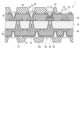
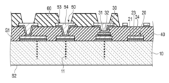
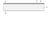
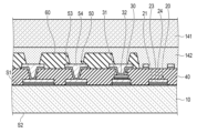
- FIG. 1 is a cross-sectional view of a wiring board according to a first embodiment of the present invention.
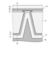
- FIG. 2 is an enlarged cross-sectional view of a part of the wiring board shown in FIG.
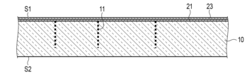
- FIG. 3 is a cross-sectional view showing one step in the method for manufacturing the wiring board shown in FIG.
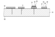
- FIG. 4 is a cross-sectional view showing another step in the method for manufacturing the wiring board shown in FIG.
- FIG. 5 is a cross-sectional view showing still another step in the method for manufacturing the wiring board shown in FIG.
- FIG. 6 is a cross-sectional view showing still another step in the method for manufacturing the wiring board shown in FIG.
- FIG. 7 is a cross-sectional view showing still another step in the method for manufacturing the wiring board shown in FIG. FIG.
- FIG. 8 is a cross-sectional view showing still another step in the method for manufacturing the wiring board shown in FIG.
- FIG. 9 is a cross-sectional view showing still another step in the method for manufacturing the wiring board shown in FIG.
- FIG. 10 is a cross-sectional view showing still another step in the method for manufacturing the wiring board shown in FIG.
- FIG. 11 is a cross-sectional view showing still another step in the method for manufacturing the wiring board shown in FIG.
- FIG. 12 is a cross-sectional view showing an example of a packaged device that can be manufactured using the wiring board shown in FIG.
- FIG. 13 is a cross-sectional view showing a part of a wiring board according to a comparative example.
- FIG. 14 is a cross-sectional view showing a through hole provided in a glass substrate of a wiring board according to a first modification.
- FIG. 15 is a cross-sectional view showing a through hole provided in a glass substrate of a wiring board according to a second modification.
- FIG. 16 is a perspective view showing a part of the wiring board according to the third modification.
- FIG. 17 is a cross-sectional view showing a part of the wiring board according to the fourth modification.
- FIG. 18 is a cross-sectional view showing a part of the wiring board according to the fifth modification.
- FIG. 19 is a cross-sectional view showing a part of the wiring board according to the sixth modification.
- FIG. 15 is a cross-sectional view showing a through hole provided in a glass substrate of a wiring board according to a second modification.
- FIG. 16 is a perspective view showing a part of the wiring board according to the third modification.
- FIG. 17 is a cross-sectional view showing a part of the
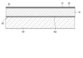
- FIG. 20 is a cross-sectional view showing one step in the method for manufacturing a wiring board according to the second embodiment of the present invention.
- FIG. 21 is a cross-sectional view showing another step in the method for manufacturing a wiring board according to the second embodiment of the present invention.
- FIG. 22 is a cross-sectional view showing one step in the method for manufacturing a wiring board according to the third embodiment of the present invention.
- FIG. 23 is a cross-sectional view showing another step in the method for manufacturing a wiring board according to the third embodiment of the present invention.
- FIG. 24 is a cross-sectional view showing one step in the method for manufacturing a wiring board according to the fourth embodiment of the present invention.
- FIG. 25 is a cross-sectional view showing another step in the method for manufacturing a wiring board according to the fourth embodiment of the present invention.
- FIG. 1 is a sectional view of a wiring board according to a first embodiment of the present invention.
- FIG. 2 is an enlarged cross-sectional view of a part of the wiring board shown in FIG.
- the wiring board 1 shown in FIG. 1 is a glass core wiring board.
- the wiring board 1 is a wiring board used as an interposer, that is, a glass interposer.
- the wiring board 1 includes a glass substrate 10, a first conductor layer 20, a dielectric layer 31, an upper electrode 32, an interlayer insulating film 40, a conductor layer 50, an insulating layer 60, and a second conductor layer 70. , an interlayer insulating film 80, a conductor layer 90, and an insulating layer 100.
- the glass substrate 10 has a first surface S1 and a second surface S2 that is the back surface thereof.
- the first surface S1 and the second surface S2 are parallel to each other.
- the glass substrate 10 is provided with one or more first through holes, each of which extends from the first surface S1 to the second surface S2, here a plurality of first through holes. Each of the first through holes tapers from the second surface S2 toward the first surface S1.
- the first conductor layer 20 is a conductor pattern provided on the first surface S1. This conductor pattern includes a land portion, a wiring portion, and a lower electrode of a capacitor 30, which will be described later.
- the first conductor layer 20 is a first wiring layer.
- the first conductor layer 20 has a multilayer structure. Specifically, the first conductor layer 20 includes a first copper layer 24 facing the first surface S1 and a hydrofluoric acid-resistant metal layer 21 interposed between the first copper layer 24 and the glass substrate 10. I'm here. As shown in FIG. 2, the first conductor layer 20 includes an adhesion layer 22 interposed between the hydrofluoric acid-resistant metal layer 21 and the first copper layer 24, and an adhesion layer 22 interposed between the adhesion layer 22 and the first copper layer 24. It further includes an intervening seed layer 23.
- the first conductor layer 20 covers the opening of the first through hole on the first surface S1 side.
- the surface of the first conductor layer 20 facing the glass substrate 10 has recesses at the positions of the first through holes.
- the hydrofluoric acid-resistant metal layer 21 has second through holes at the positions of the first through holes. These second through holes form the above-mentioned recesses on the surface of the first conductor layer 20 facing the glass substrate 10.
- the outline of each opening (hereinafter sometimes referred to as the first opening) of the recess provided in the surface of the first conductor layer 20 is the opening on the first surface S1 side of the corresponding first through hole (hereinafter referred to as the first opening). , the second opening) and surrounding it. That is, the outline of the orthogonal projection of the first opening onto a plane perpendicular to the thickness direction of the wiring board 1 is larger than and surrounds the orthogonal projection of the second opening onto this plane.
- the distance from the contour of the orthogonal projection of the first opening onto the above-mentioned plane to the orthogonal projection of the second opening onto this plane, that is, the width of the undercut portion caused by side etching, which will be described later, is, for example, 1 ⁇ m to 10 ⁇ m. According to another example, it is within the range of 0.1 ⁇ m to 5 ⁇ m.
- the hydrofluoric acid-resistant metal layer 21 is made of a metal material that is more resistant to etching by hydrofluoric acid than the glass substrate 10.
- the hydrofluoric acid-resistant metal layer 21 is made of a material selected from the group consisting of chromium, nickel, and nickel-chromium alloys.
- the thickness T3 of the hydrofluoric acid-resistant metal layer 21 is preferably in the range of 10 nm to 500 nm, and more preferably in the range of 0.02 ⁇ m to 0.08 ⁇ m.
- the adhesion layer 22 and the seed layer 23 are laminated in this order on the hydrofluoric acid-resistant metal layer 21.
- the adhesion layer 22 and the seed layer 23 can be made of the materials exemplified for the adhesion layer 72 and the seed layer 73 described below, respectively.
- the adhesion layer 72 and the seed layer 73 are provided when the first copper layer 24 is formed by electrolytic plating.
- the adhesion layer 72 may be omitted.
- both the adhesion layer 22 and the seed layer 23 may be omitted.
- the dielectric layer 31 and the upper electrode 32 are laminated in this order on a part of the first conductor layer 20.
- the portion of the first conductor layer 20 that faces the upper electrode 32 is a lower electrode.
- the upper electrode 32, dielectric layer 31, and lower electrode constitute a capacitor 30, specifically an MIM capacitor.
- the lower electrode covers the opening of the first through hole on the first surface S1 side.
- the lower electrode may be spaced apart from the first through hole, but if it is provided so as to cover the opening on the first surface S1 side of the first through hole, it is possible to reduce the electrical resistance caused by the wiring and to reduce the wiring length. can be shortened.
- the capacitor 30 is installed here so as to face the first surface S1, the capacitor may be installed on the second surface S2 side. Alternatively, the capacitor 30 may be installed so as to face the first surface S1, and another capacitor may be further installed on the second surface S2 side. Capacitor 30 can be omitted.
- the interlayer insulating film 40 covers the first surface S1 and buries the first conductor layer 20, dielectric layer 31, and upper electrode 32. Through holes are provided in the interlayer insulating film 40 at the positions of the land portions included in the first conductor layer 20 and at the positions of the upper electrodes 32 .
- the interlayer insulating film 40 is an insulating resin layer.
- the conductor layer 50 is a conductor pattern provided on the interlayer insulating film 40.
- This conductor pattern includes a pad portion provided on the main surface of the interlayer insulating film 40 and a via portion covering the side wall of the through hole provided in the interlayer insulating film 40.
- the pad portion is an external connection terminal.
- Each via portion connects the land portion or upper electrode 32 included in the first conductor layer 20 to the pad portion.
- the conductor layer 50 includes a seed layer 53 and a copper layer 54.
- the seed layer 53 and the copper layer 54 are laminated in this order on the interlayer insulating film 40.
- the conductor layer 50 may further include an adhesion layer between the interlayer insulating film 40 and the seed layer 53.
- materials exemplified for the adhesion layer 72 and the seed layer 73, which will be described later, can be used, respectively.
- the seed layer 53 may be omitted.
- the insulating layer 60 at least partially covers the interlayer insulating film 40 and embeds the conductor layer 50.
- a through hole is provided in the insulating layer 60 at a position of a pad portion included in the conductor layer 50 .
- the insulating layer 60 is made of, for example, solder resist.
- the second conductor layer 70 is a conductor pattern including a portion covering the second surface S2 of the glass substrate 10, a portion covering the sidewall of the first through hole provided in the glass substrate 10, and a portion covering the inner surface of the recess provided in the first conductor layer 20.
- This conductor pattern includes a land portion, a wiring portion, and a via portion.
- the portion of the second conductor layer 70 covering the second surface S2 is the second wiring layer, and includes a land portion and a wiring portion.
- the via portion consists of a portion of the second conductor layer 70 covering the sidewall of the first through hole provided in the glass substrate 10, and a portion covering the inner surface of the recess provided in the first conductor layer 20.
- the second conductor layer 70 has a multilayer structure. Specifically, the second conductor layer 70 includes an adhesion layer 72, a seed layer 73, and a second copper layer 74, as shown in FIG. The adhesion layer 72, the seed layer 73, and the second copper layer 74 are laminated in this order on the glass substrate 10.
- the adhesion layer 72 covers the side wall of the first through hole provided in the glass substrate 10, the inner surface of the recess provided in the first conductor layer 20, and the second surface S2 side of the first through hole of the second surface S2. It covers the area surrounding the opening. Adhesion layer 72 is conformal to these surfaces.
- the adhesion layer 72 enhances the adhesion of the seed layer 73 to the glass substrate 10.
- the adhesion layer 72 is preferably made of one or more materials selected from the group consisting of titanium, chromium, and nickel, or an oxide thereof, and more preferably made of titanium or titanium oxide.
- the thickness T1 of the adhesion layer 72 is preferably in the range of 10 nm to 0.5 ⁇ m, and more preferably in the range of 20 nm to 0.08 ⁇ m.
- the thickness T1 of the adhesion layer 72 is the thickness of the portion of the adhesion layer 72 provided on the second surface S2.
- the thickness T1 of the adhesive layer 72 and the thickness T2 of the seed layer 73 it is advantageous to increase the thickness T1.
- the connection resistance between the first conductor layer 20 and the second conductor layer 70 increases.
- the seed layer 73 is provided on the adhesive layer 72. Seed layer 73 is conformal to adhesion layer 72 .
- the seed layer 73 serves as a power supply layer in electrolytic plating. Seed layer 73 is made of copper, for example.
- the thickness T2 of the seed layer 73 is preferably in the range of 100 nm to 0.5 ⁇ m, more preferably in the range of 200 nm to 0.4 ⁇ m. Here, the thickness T2 of the seed layer 73 is the thickness of the portion of the seed layer 73 provided on the second surface S2.
- the seed layer 73 is preferably thick.
- the second copper layer 74 is removed as unnecessary parts such as the seed layer 73 formed as a continuous film are removed by etching the entire surface. The surface area of is also removed. Therefore, when the thickness T2 is increased, the shape accuracy and dimensional accuracy of the wiring included in the second conductor layer 70 decreases.
- the second copper layer 74 is provided on the seed layer 73.
- Second copper layer 74 is conformal to seed layer 73 .
- the thickness of the second copper layer 74 is, for example, in the range of 2 ⁇ m to 10 ⁇ m.
- the total thickness T1+T2 of the thickness T1 of the adhesive layer 72 and the thickness T2 of the seed layer 73 is equal to or larger than the thickness T3 of the hydrofluoric acid-resistant metal layer 21. That is, the thicknesses T1 to T3 satisfy the relationship shown in inequality (1) below. T3 ⁇ T1+T2...(1)
- the total T1+T2 is preferably larger than the thickness T3, more preferably twice or more the thickness T3, and even more preferably six times or more the thickness T3.
- the thicknesses T2 and T3 may satisfy the relationship shown in inequality (1) below.
- the seed layer 73 forms an undercut between the bottom surface of the recess provided in the first conductor layer 20 and the side wall of the first through hole. Less likely to cause discontinuities due to Therefore, in electrolytic plating for forming the second copper layer 74, insufficient copper deposition within the recesses provided in the first conductor layer 20 is unlikely to occur.
- the total T1+T2 is preferably 20 times or less than the thickness T3, and more preferably 8 times or less than the thickness T3.
- unnecessary portions of the adhesion layer 72 and the seed layer 73, which are formed as a continuous film, are removed by etching the entire surface. If the total T1+T2 is increased, the time required to remove these unnecessary portions will be longer.
- the thickness T2 is equal to or larger than the sum T1+T3 of the thickness T1 and the thickness T3. That is, it is preferable that the thicknesses T1 to T3 satisfy the relationship shown in inequality (3) below. T1+T3 ⁇ T2...(3)
- the seed layer 73 is thicker than the hydrofluoric acid-resistant metal layer 21 and the adhesive layer 72. When such a configuration is adopted, the seed layer 73 can exhibit particularly excellent performance as a power supply layer during electrolytic plating to form the second copper layer 74.
- the interlayer insulating film 80 covers the second surface S2 and embeds the second conductor layer 70.
- a through hole is provided in the interlayer insulating film 80 at the position of the land portion included in the second conductor layer 70 .
- the interlayer insulating film 40 is an insulating resin layer.
- the conductor layer 90 is a conductor pattern provided on the interlayer insulating film 80.
- This conductor pattern includes a pad portion provided on the main surface of the interlayer insulating film 80 and a via portion covering the side wall of the through hole provided in the interlayer insulating film 80.
- the pad portion is an external connection terminal.
- Each via portion connects a land portion included in the second conductor layer 70 to a pad portion.
- the conductor layer 90 includes a seed layer 93 and a copper layer 94.
- the seed layer 93 and the copper layer 94 are laminated in this order on the interlayer insulating film 80.
- the conductor layer 90 may further include an adhesion layer between the interlayer insulating film 80 and the seed layer 93.
- the materials exemplified for the adhesion layer 72 and the seed layer 73 can be used for the adhesion layer and the seed layer 93 included in the conductor layer 90, respectively. Seed layer 93 may be omitted.
- the insulating layer 100 at least partially covers the interlayer insulating film 80 and embeds the conductor layer 90.
- a through hole is provided in the insulating layer 100 at a position of a pad portion included in the conductor layer 90.
- Insulating layer 100 is made of, for example, solder resist.
- the wiring board 1 described above can be manufactured, for example, by the following method.
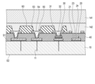
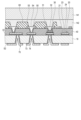
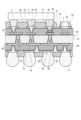
- 3 to 11 are cross-sectional views showing a method of manufacturing the wiring board shown in FIG. 1.
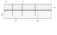
- a glass substrate 10 having a first surface S1 and a second surface S2 which is the back surface thereof is prepared.
- the glass substrate 10 is obtained by removing contaminants from the surface of a 500 ⁇ m thick alkali-free glass plate by ultrasonic cleaning or the like.
- the glass substrate 10 at this stage is thicker than the glass substrate 10 included in the wiring board 1.
- the glass substrate 10 at this stage is a large-sized glass substrate whose dimension in the direction perpendicular to the thickness direction is larger than that of the glass substrate 10 included in a packaged device to be described later.
- the glass substrate 10 is irradiated with a laser beam from the first surface S1 toward the second surface S2, and as shown in FIG. A modified portion 11 is formed.
- the modified portion 11 is, for example, a portion that is heated by laser beam irradiation and has a difference in crystallinity or the like from the laser beam unirradiated portion.
- the modified portion 11 is formed at a position corresponding to the first through hole.
- the modified portion 11 extends from the first surface S1 toward the second surface S2, for example, in the thickness direction of the glass substrate 10. It is desirable to adjust the amount of laser light so that the modified portion 11 extending from the first surface S1 does not reach the second surface S2.
- the wavelength of the laser light used here is 535 nm or less.
- the preferable wavelength of the laser beam is 355 nm or more and 535 nm or less. If the wavelength of the laser beam is less than 355 nm, it may be difficult to obtain sufficient laser output, and stable laser modification may become difficult. On the other hand, if the wavelength of the laser beam is made larger than 535 nm, the irradiation spot becomes large, making it difficult to modify a small area with the laser. Furthermore, microcracks occur due to the influence of heat, making the glass substrate 10 more likely to break.
- the laser pulse width is preferably in the range of picoseconds to femtoseconds.
- the laser pulse width is longer than nanoseconds, it becomes difficult to control the amount of energy per pulse, microcracks occur, and the glass substrate 10 becomes easily broken.
- a preferable value for the energy of the laser pulse is selected depending on the composition of the glass and what kind of laser modification is to be caused, and it is preferably within the range of 5 ⁇ J or more and 150 ⁇ J or less. By increasing the energy of the laser pulse, it becomes possible to increase the length of the modified portion 11 in proportion to the energy.
- a hydrofluoric acid-resistant metal layer 21 and a seed layer 23 are formed in this order on the first surface S1.
- each of the hydrofluoric acid-resistant metal layer 21 and the seed layer 23 is formed as a continuous film.
- the hydrofluoric acid-resistant metal layer 21 is formed, for example, by sputtering.
- the seed layer 23 is formed, for example, by sputtering or electroless plating.
- an adhesion layer 22 shown in FIG. 2 may be formed on the hydrofluoric acid-resistant metal layer 21.
- the adhesive layer 22 is formed as a continuous film by, for example, sputtering or electroless plating. Forming the adhesion layer 22 improves the adhesion between the hydrofluoric acid-resistant metal layer 21 and the seed layer 23.
- a mask pattern made of an insulator and having openings at positions corresponding to the first copper layer 24 is formed on the seed layer 23 .
- the mask pattern is formed, for example, by providing a photoresist layer on the seed layer 23 and subjecting the photoresist layer to pattern exposure and development.
- a dry photoresist RD1225 manufactured by Showa Denko Materials Co., Ltd. is laminated onto the seed layer 23, and a mask pattern made of resin is obtained by sequentially performing pattern exposure and development on this dry photoresist.
- electrolytic copper plating is performed using the seed layer 23 as a power supply layer.
- copper is deposited on the seed layer 23 at the openings of the mask pattern, thereby obtaining the first copper layer 24 shown in FIG. 5.
- the mask pattern is removed.
- the dry film resist is dissolved and peeled off.
- the entire surface of the composite including the first copper layer 24 and the glass substrate 10 on the side of the first copper layer 24 is etched until the exposed portion of the seed layer 23 is removed.
- an adhesion layer 22 is present between the seed layer 23 and the hydrofluoric acid-resistant metal layer 21, the entire surface of the composite on the side of the first copper layer 24 is further etched until the portion of the adhesion layer 22 exposed by removing the exposed portion of the seed layer 23 is also removed.
- the first conductor layer 20 shown in FIG. 5 is obtained. Note that, as described above, the first conductor layer 20 includes a land portion, a wiring portion, and a lower electrode.
- a dielectric layer 31 and an upper electrode 32 are formed in this order on the lower electrode included in the first conductor layer 20, to obtain the capacitor 30 shown in FIG. 5.
- the upper electrode 32 can be formed, for example, by the same method as described above for the seed layer 23 and first copper layer 24 included in the first conductor layer 20.
- Such an upper electrode 32 has a multilayer structure including a seed layer and a copper layer.
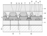
- an insulating resin layer is provided on the surface of the composite body including the capacitor 30 and the glass substrate 10 on the capacitor 30 side.
- an insulating resin film ABF-GXT31 (32.5 ⁇ m thick) manufactured by Ajinomoto Fine Techno Co., Ltd. is laminated onto the above surface, and this is pre-cured.
- blind vias are formed in the insulating resin layer by laser processing.
- a desmear process is performed to remove the residue generated by laser processing. In the manner described above, the interlayer insulating film 40 shown in FIG. 6 is obtained.
- a seed layer 53 is formed by sputtering or electroless plating.
- the seed layer 53 covers the upper surface of the interlayer insulating film 40, the side walls of the through holes provided therein, and the portions of the first conductor layer 20 and the upper electrode 32 exposed at the positions of these through holes. Form it like this.
- a mask pattern made of an insulator and having openings at positions corresponding to the copper layer 54 is formed on the seed layer 53.
- the mask pattern is formed, for example, by providing a photoresist layer on the seed layer 53 and performing pattern exposure and development on this photoresist layer.
- a dry film resist RD1225 manufactured by Showa Denko Materials Co., Ltd. is laminated onto the seed layer 53, and a mask pattern made of resin is obtained by sequentially performing pattern exposure and development on this dry film resist.
- the mask pattern is removed.
- the dry film resist is dissolved and peeled off.
- the entire surface of the composite including the copper layer 54 and the glass substrate 10 on the copper layer 54 side is etched until the exposed portion of the seed layer 53 is removed. In this manner, the conductor layer 50 is obtained.
- an insulating layer 60 as shown in FIG. 6 is provided on the interlayer insulating film 40.
- a solder resist is provided on the interlayer insulating film 40, and then patterned using a photolithography method or the like. In this manner, the structure shown in FIG. 6 is obtained.
- the composite including the glass substrate 10 and the insulating layer 60 is placed on the second support 141, and the insulating layer 60 Support it so that it faces 141.
- the second support 141 is bonded to the above-mentioned composite body via an adhesive 142 for temporary bonding.
- the second support 141 makes it difficult to damage the glass substrate 10 due to its thinning in the next step, and facilitates handling of the composite including the glass substrate 10.
- the adhesive 142 for example, Riva Alpha (registered trademark) manufactured by Nitto Denko Corporation is used.
- Riva Alpha registered trademark
- the second support 141 for example, a thin glass carrier is used.
- the second support body 141 does not need to be made of glass, and may be made of metal, resin, or the like.
- the thickness of the second support 141 is desirably within the range of 0.7 mm or more and 10 mm or less, considering the transportability of the glass substrate 10 after it is thinned.
- the thickness of the second support 141 may be set as appropriate depending on the thickness of the glass substrate 10.
- the second surface S2 of the composite supported on the second support 141 is etched with an etching solution containing hydrogen fluoride, as shown in FIG. Then, the second surface S2 is retreated, and the first through holes 12 are formed at the positions of the modified portions 11, respectively.
- the glass substrate 10 becomes thinner and the modified portion 11 is exposed.
- the modified portion 11 of the glass substrate 10 has a higher etching rate than other portions. Therefore, by this etching, it is possible to simultaneously achieve thinning of the glass substrate 10 and formation of the first through hole 12.
- the hydrofluoric acid-resistant metal layer 21 serves as an etching stopper film.
- the first through hole 12 obtained by the above etching has a truncated conical shape in which the diameter (or cross-sectional area) on the second surface S2 side is larger than the diameter (or cross-sectional area) on the first surface S1 side. have.
- the amount of etching of the glass substrate 10 may be set as appropriate depending on the thickness of the wiring board 1. For example, if the thickness of the glass substrate 10 before etching is 400 ⁇ m, the etching amount is preferably within the range of 100 ⁇ m or more and 350 ⁇ m or less. The thickness of the glass substrate 10 after thinning is preferably within the range of 50 ⁇ m or more and 300 ⁇ m or less.
- the etching solution containing hydrogen fluoride is, for example, a hydrogen fluoride aqueous solution.
- the etching solution can further contain one or more inorganic acids selected from the group consisting of nitric acid, hydrochloric acid, and sulfuric acid.
- the hydrogen fluoride concentration of the etching solution is, for example, in the range of 1.0% by mass or more and 6.0% by mass or less, preferably in the range of 2.0% by mass or more and 5.0% by mass or less.
- the inorganic acid concentration is, for example, in the range of 1.0% by mass or more and 20.0% by mass or less, preferably in the range of 3.0% by mass or more and 16.0% by mass or less. It is desirable to perform etching at an etching rate of 1.0 ⁇ m/min or less using an etching solution in which the concentration of each component is set within the above range.
- the temperature of the etching solution during etching is desirably within the range of 10°C or more and 40°C or less.
- the portion of the hydrofluoric acid-resistant metal layer 21 exposed within the first through hole 12 is subjected to wet etching to form the first conductor layer 20 as shown in FIG. A recess is formed on the surface of the glass substrate 10 side.
- the wet etching of the hydrofluoric acid-resistant metal layer 21 is performed so that a second through hole is formed in the hydrofluoric acid-resistant metal layer 21.
- Any etchant may be used for this wet etching as long as it can remove the exposed portion of the hydrofluoric acid-resistant metal layer 21.
- this etching solution a chromium etching solution is suitably used.
- an alkaline chromium etching solution manufactured by Nihon Kagaku Sangyo Co., Ltd. containing potassium ferricyanide and potassium hydroxide is used as the etching solution. Then, using this etching solution, wet etching is performed at a temperature of 40° C. for 1.5 minutes. According to such wet etching, exposed portions of the hydrofluoric acid-resistant metal layer 21 can be removed without damaging components other than the hydrofluoric acid-resistant metal layer 21, such as the glass substrate 10, the first copper layer 24, and the interlayer insulating film 40. can only be removed.
- the first through hole 12 has a truncated conical shape in which the diameter (or cross-sectional area) on the second surface S2 side is larger than the diameter (or cross-sectional area) on the first surface S1 side. .
- Such a shape promotes circulation of the etching solution between the inside and outside of the first through-hole 12 and enables efficient etching.
- a plasma treatment using CF4 gas, oxygen gas, argon gas, or hydrogen gas, or ultrasonic cleaning it is preferable to carry out, for example, a plasma treatment using CF4 gas, oxygen gas, argon gas, or hydrogen gas, or ultrasonic cleaning, to improve the wettability of the exposed portion of the hydrofluoric acid-resistant metal layer 21 to the etching solution. It is more preferable to carry out both the plasma treatment and ultrasonic cleaning. In this case, the wettability improvement effect is further enhanced.
- the adhesive layer 72 shown in FIG. 2 is formed.
- the adhesion layer 72 is formed as a continuous film that covers the side wall of the first through hole 12, the inner surface of the recess formed in the first conductor layer 20, and the second surface S2.
- the adhesive layer 72 is formed as a continuous film by, for example, sputtering or electroless plating. In order to deposit metal on the undercut portion, which will be described later, it is preferable that the adhesive layer 72 be formed by electroless plating.
- a seed layer 73 shown in FIG. 10 is formed on the adhesive layer 72.
- the seed layer 73 is formed as a continuous film by, for example, sputtering or electroless plating. In order to deposit metal into the undercut portion, it is preferable that the seed layer 73 be formed by electroless plating.
- the adhesion layer 72 and the seed layer 73 are formed so that the thickness T1 of the adhesion layer 72, the thickness T2 of the seed layer 73, and the thickness T3 of the hydrofluoric acid-resistant metal layer satisfy the above-mentioned relationship.
- a second copper layer 74 is formed on the seed layer 73.
- a mask pattern made of an insulator and having openings at positions corresponding to the second copper layer 74 is formed on the seed layer 73 .
- the mask pattern is formed, for example, by providing a photoresist layer on the seed layer 73 and performing pattern exposure and development on this photoresist layer.
- a dry photoresist RD1225 manufactured by Showa Denko Materials Co., Ltd. is laminated onto the seed layer 73, and a mask pattern made of resin is obtained by sequentially performing pattern exposure and development on this dry photoresist.
- electrolytic copper plating is performed using the seed layer 73 as a power supply layer. This causes copper to be deposited on the seed layer 73 at the positions of the openings in the mask pattern, resulting in the second copper layer 74 shown in FIG. 10.
- the mask pattern For example, a dry film resist is dissolved and peeled off.
- the entire surface of the composite including the second copper layer 74 and the glass substrate 10 on the second copper layer 74 side is etched to remove the exposed portion of the seed layer 73.
- the entire surface of the composite on the second copper layer 74 side is further etched until the exposed portion of the adhesive layer 72 is removed by removing the exposed portion of the seed layer 73.
- the second conductor layer 70 shown in FIG. 10 is obtained. Note that, as described above, the second conductor layer 70 includes a land portion and a wiring portion.
- FIG. 12 is a cross-sectional view showing an example of a packaged device that can be manufactured using the wiring board shown in FIG.
- the packaged device shown in FIG. 12 is, for example, a high frequency device equipped with an LC filter.
- the packaged device shown in FIG. 12 includes a wiring board 1, a functional device 2, a chip component 3, and bonding conductors 4 and 5.
- the wiring board 1 is obtained by dividing the wiring board described with reference to FIG. 1 etc. into pieces.
- the wiring board 1 can further include at least one of the bonding conductors 4 and 5.
- the bonding conductors 4 and 5 are solder balls here.
- the bonding conductor 4 is provided on the pad portion included in the conductor layer 50.
- the bonding conductor 4 bonds the functional device 2 to the wiring board 1 .
- the bonding conductor 5 is provided on the pad portion included in the conductor layer 90.
- the bonding conductor 5 allows the packaged device to be bonded to another wiring board, such as a motherboard.
- the functional device 2 is a device that operates by being supplied with at least one of electric power and an electric signal, a device that outputs at least one of electric power and an electric signal by external stimulation, or a device that outputs at least one of electric power and an electric signal.
- a device that operates when at least one of them is supplied and outputs at least one of electric power and an electric signal when stimulated from the outside.
- the functional device 2 is in the form of a chip, such as a semiconductor chip or a chip in which circuits and elements are formed on a substrate made of a material other than a semiconductor, such as a glass substrate.
- the functional device 2 can include, for example, one or more of an LSI, a memory, an image sensor, a light emitting device, and a MEMS.
- the MEMS is, for example, one or more of a pressure sensor, an acceleration sensor, a gyro sensor, a tilt sensor, a microphone, and an acoustic sensor.
- the functional device is a semiconductor chip including an LSI.
- the functional device 2 is mounted on the wiring board 1.
- the functional device 2 is mounted on the wiring board 1 by flip-chip bonding.
- Functional device 2 may be mounted on wiring board 1 using other surface mounting techniques.
- a packaged device may include two or more functional devices 2.
- the chip components 3 are passive components that can be surface mounted, such as chip resistors, chip capacitors, and chip inductors.
- Chip component 3 is mounted on wiring board 1.
- the chip component 3 is mounted on the wiring board 1 by die bonding and wire bonding.
- Chip component 3 may be mounted on wiring board 1 using other surface mounting techniques.
- the packaged device may include two or more chip components 3.
- the chip component 3 may be omitted.
- the chip component 3 is a chip inductor, and together with the capacitor 30 constitutes an LC filter.
- the glass substrate 10 is less likely to be damaged, and excellent handling properties can be achieved. This will be explained below.
- a through hole is formed in a glass substrate, its mechanical strength may decrease. Further, a glass substrate having a small thickness, for example, a glass substrate having a thickness of 300 ⁇ m or less, is difficult to handle because it is easily cracked during transportation for forming a conductive part such as a circuit.
- the composite body including the glass substrate 10 and the first conductor layer 20 has high strength even after the glass substrate 10 is thinned and the first through holes 12 are formed. Therefore, damage to the glass substrate 10 is unlikely to occur in subsequent steps as well.
- the second support body 141 further makes it difficult for the glass substrate 10 to be damaged. Furthermore, since the strength of the composite is increased by forming the second conductor layer 70 and the like before removing the second support 141, the strength of the composite is increased. However, damage to the glass substrate 10 is unlikely to occur. Therefore, according to the manufacturing method described above, the glass substrate 10 is less likely to be damaged and is easy to handle.
- the first through hole 12 is also formed by wet etching to thin the glass substrate 10. Then, the first through hole 12 is formed at the position of the modified portion 11 caused by laser beam irradiation.
- the modified portion 11 of the glass substrate 10 can be etched at a higher etching rate than other portions. Therefore, according to the manufacturing method described above, high productivity can be achieved.
- the wiring board 1 obtained by the method described above has electrical properties of the connection portion between the wiring layer provided on the glass substrate 10 and the TGV provided on this glass substrate. Are better.
- FIG. 13 is a cross-sectional view showing a part of a wiring board according to a comparative example.
- the first through hole 12 is formed in the glass substrate 10 by performing etching using an etching solution containing hydrogen fluoride.
- the structure immediately after this etching has an etching residue 10ER (also referred to as glass residue) of the glass substrate 10 on the hydrofluoric acid-resistant metal layer 21 inside the first through hole 12.
- the etching residue 10ER inhibits the electrical connection between the first conductor layer 20 and the second conductor layer 70. .
- the portion of the hydrofluoric acid-resistant metal layer 21 exposed at the position of the first through hole 12 is removed by wet etching. Since wet etching is isotropic etching, when this etching is performed, the portion of the hydrofluoric acid-resistant metal layer 21 located directly below the etching residue 10ER is also removed by side etching. Therefore, when this etching is performed, the etching residue 10ER is also removed. Additionally, the material of the hydrofluoric acid-resistant metal layer 21 generally has a higher electrical resistivity than copper or the like. Therefore, by removing the portion of the hydrofluoric acid-resistant metal layer 21 exposed at the position of the first through hole 12, the connection resistance between the first conductor layer 20 and the second conductor layer 70 can be reduced.
- the portion of the hydrofluoric acid-resistant metal layer 21 exposed at the position of the first through hole 12 is removed by wet etching, which is isotropic etching. Therefore, as shown in FIG. 2, in the hydrofluoric acid-resistant metal layer 21, only the portion corresponding to the opening on the first surface S1 side of the first through hole 12 is removed, but the opening is removed by side etching. Surrounding parts are also removed. That is, an undercut portion is formed in the hydrofluoric acid-resistant metal layer 21. This undercut portion increases the contact area between the first conductor layer 20 and the second conductor layer 70.
- the wiring board 1 obtained by the method described above has excellent electrical characteristics at the connection portion between the wiring layer provided on the glass substrate 10 and the TGV provided on this glass substrate.
- the wiring board 1 obtained by the method described above has connection reliability between the wiring layer provided on the glass substrate 10 and the TGV provided on this glass substrate. Excellent.
- the etching residue 10ER shown in FIG. 13 reduces the adhesion between the hydrofluoric acid-resistant metal layer 21 and the second conductor layer 70, and therefore reduces the connection reliability between the first conductor layer 20 and the second conductor layer 70. It can be done.
- the portion of the hydrofluoric acid-resistant metal layer 21 exposed at the position of the first through hole 12 is removed by wet etching. When the portion of the hydrofluoric acid-resistant metal layer 21 exposed at the position of the first through hole 12 is removed, the etching residue 10ER located on this portion is also removed.
- connection portion between the first conductor layer 20 and the second conductor layer 70. Therefore, disconnection at this connection has a large effect on connection reliability.
- the hydrofluoric acid-resistant metal layer 21 has an undercut portion, and the second conductor layer 70 at least partially embeds the undercut portion.
- the portion of the second conductor layer 70 in which the undercut portion is embedded makes it difficult for the portion located within the first through hole 12 to move when a force is applied to the portion of the composite layer of the seed layer 73 and the second copper layer 74 located within the first through hole 12 in a direction that pulls it away from the first conductor layer 20.
- the wiring board 1 obtained by the method described above has excellent connection reliability between the wiring layer provided on the glass substrate 10 and the TGV provided on this glass substrate.
- the wet etching performed in the eighth step produces an undercut portion in the hydrofluoric acid-resistant metal layer 21, as shown in FIG.
- the undercut portion includes the side wall of the first through hole 12 and the bottom surface of the recess formed in the first conductor layer 20.
- the material of the adhesive layer 72 and the material of the seed layer 73 are difficult to deposit compared to the region corresponding to the opening on the side S1. Therefore, if the total T1+T2 of the thickness T1 of the adhesive layer 72 and the thickness T2 of the seed layer 73 is smaller than the thickness T3 of the hydrofluoric acid-resistant metal layer 21, there will be a discontinuity near the undercut part.
- a seed layer 73 having a portion may be formed. For example, there is a possibility that the seed layer 73 having an annular discontinuous portion surrounding the opening on the first surface S1 side of the first through hole 12 is formed.
- the seed layer 73 has such a discontinuous portion, power cannot be supplied to the portion of the seed layer 73 surrounded by the annular discontinuous portion in the electrolytic copper plating performed in the tenth step. .
- a void may be generated between the second copper layer 74 and the portion of the seed layer 73 surrounded by the annular discontinuity at the position of the recess formed in the first conductor layer 20. That is, a disconnection occurs between the wiring layer provided on the glass substrate 10 and the TGV provided on this glass substrate.
- the sum T1+T2 of the thickness T1 of the adhesive layer 72 and the thickness T2 of the seed layer 73 is made equal to the thickness T3 of the hydrofluoric acid-resistant metal layer 21, or Make it larger than this. If the adhesion layer 72 and the seed layer 73 are formed so as to satisfy this relationship, it is possible to reliably prevent the above-mentioned discontinuous portion from occurring in the seed layer 73. Therefore, the generation of the above-mentioned voids can be prevented. Therefore, disconnection between the wiring layer provided on the glass substrate 10 and the TGV provided on this glass substrate can be made less likely to occur, and a high yield can be achieved.
- the thickness T1 is preferably equal to or larger than the thickness T3. If the adhesion layer 72 is formed so as to satisfy this relationship, it is possible to more reliably prevent the above-mentioned discontinuous portion from occurring in the seed layer 73.
- thickness T2 is preferably equal to or greater than the sum T1+T3 of thickness T1 and thickness T3. If the power supply to the portion of seed layer 73 located within first through hole 12 during electrolytic plating to form second copper layer 74 is insufficient, the deposition of copper within first through hole 12 will be insufficient, which may cause a disconnection between the wiring layer provided on glass substrate 10 and the TGV provided on this glass substrate. If adhesion layer 72 and seed layer 73 are formed so as to satisfy the above relationship, the above disconnection caused by insufficient power supply can be made less likely to occur.
- FIG. 14 is a cross-sectional view showing a through hole provided in the glass substrate of the wiring board according to the first modification.
- FIG. 15 is a cross-sectional view showing a through hole provided in a glass substrate of a wiring board according to a second modification.
- the wiring boards according to the first and second modifications are the same as the wiring board 1 described above, except that the structures shown in FIGS. 14 and 15 are respectively adopted for the first through hole 12.
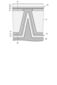
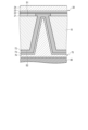
- the first through hole 12 provided in the glass substrate 10 tapers from the second surface S2 toward the first surface S1. That is, the first through hole 12 has a forward tapered shape. As shown in FIGS. 14 and 15, the first through hole 12 has a forward tapered portion that tapers from the second surface S2 to the first surface S1 and a tapered portion that tapers from the first surface S1 to the second surface S2. It may also include a reverse tapered portion.
- the forward tapered portion extends from the second surface S2 toward the first surface S1, and decreases in diameter from the second surface S2 toward the first surface S1. Further, the reverse tapered portion extends from the first surface S1 toward the second surface S2, and increases in diameter from the first surface S1 toward the second surface S2.
- the position where the first through hole 12 has the minimum diameter is within a distance from the first surface S1 of 0.4 to 0.6 times the thickness T of the glass substrate 10. It is in.
- the distance from the first surface S1 to the position where the first through hole 12 has the minimum diameter is 0.2 times or less the thickness T of the glass substrate 10.
- the position where the first through hole 12 has the minimum value of the diameter (or the position where the area of the cross section parallel to the first surface S1 has the minimum value) is located on the first surface. It is separated from S1. Therefore, when the structure shown in FIG. 14 or 15 is adopted for the first through hole 12, the connection between the first conductor layer 20 and the second conductor layer 70 is The applied stress can be reduced, and therefore the connection reliability between the wiring layer provided on the glass substrate 10 and the TGV provided on this glass substrate can be further improved.
- the packaged device described above includes an inductor as the chip component 3.
- an LC filter can be configured by combining the inductor and capacitor 30.
- the inductor may be built into the wiring board 1.
- an inductor is built into the wiring board 1, it is possible, for example, to shorten the wiring length, thereby improving the electrical characteristics and transmission characteristics, or to make the packaged device smaller or lower in height.
- the inductor built into the wiring board 1 is, for example, a spiral coil.
- the wiring board 1 may include a portion of the first conductor layer 20 as a spiral coil, and may include a portion of the second conductor layer 70 as a spiral coil.
- the wiring board 1 may include a portion of the first conductor layer 20 as a spiral coil and a portion of the second conductor layer 70 as another spiral coil.
- the wiring board 1 may include a solenoid coil described below as an inductor.
- FIG. 16 is a perspective view showing a part of the wiring board according to the third modification.
- FIG. 16 depicts a solenoid coil 110 as an example of an inductor that can be built into the wiring board 1.
- the wiring board according to the third modification is the same as the wiring board 1 described above except that it includes the solenoid coil 110.
- the solenoid coil 110 is composed of a part of the first conductor layer 20 and a part of the second conductor layer 70. Specifically, the solenoid coil 110 includes a first conductor path 20A, a second conductor path 70A, and a third conductor path 70B.
- Each of the first conductor paths 20A is a part of the first conductor layer 20.
- the first conductor path 20A has a shape extending in a first direction parallel to the first surface S1, and extends in a second direction parallel to the first surface S1 and intersecting the first direction. Arranged at a constant pitch.
- Each first conductor path 20A has a first end and a second end.
- the glass substrate 10 is provided with first through holes 12 at a first end position and a second end position.
- Each of the second conductor paths 70A is a part of the second conductor layer 70 located on the second surface S2.
- the second conductor paths 70A have a shape extending in a third direction that is parallel to the second surface S2 and intersects with the first and second directions, and are arranged at a constant pitch in the second direction. ing.
- Each second conductor path 70A has a third end facing the first end of a certain first conductor path 20A, and a second end of the first conductor path 20A adjacent to the previous first conductor path 20A. and a third end.
- Each of the third conductor paths 70B is a part of the second conductor layer 70 located inside the first through hole 12.
- the third conductor path 70B connects the third end and fourth end of each second conductor path 70A to the first end of a certain first conductor path 20A and the first end of the adjacent first conductor path 20A, respectively. It is connected to the two ends.
- the solenoid coil 110 has a structure in which a plurality of segments each including a first conductor path 20A, a third conductor path 70B, a second conductor path 70A, and a third conductor path 70B are connected in series in this order. Further, the helical axis of the solenoid coil 110 is parallel to the second direction. Solenoid coil 110 may be combined with capacitor 30 to configure an LC filter.
- connection resistance between the first conductor layer 20 and the second conductor layer 70 is large. Therefore, when the connection portion between the first conductor path 20A and the third conductor path 70B has the structure described with reference to FIG. 13, the connection resistance between the first conductor path 20A and the third conductor path 70B is large. Therefore, in this case, it is difficult to realize an LC filter with excellent electrical characteristics and transmission characteristics, particularly transmission characteristics in a high frequency band.
- connection portion between the first conductor path 20A and the third conductor path 70B has the structure described with reference to FIG. 2.
- the connection resistance between the first conductor layer 20 and the second conductor layer 70 is small. Therefore, in the solenoid coil 110, the connection resistance between the first conductor path 20A and the third conductor path 70B is small. Therefore, when this solenoid coil 110 is combined with the capacitor 30, it is possible to realize an LC filter with excellent electrical characteristics and transmission characteristics.
- the solenoid coil 110 is composed of a part of the first conductor layer 20 and a part of the second conductor layer 70.
- a solenoid coil having a similar structure can be composed of a part of the first conductor layer 20 and a part of the conductor layer 50, and can be composed of a part of the second conductor layer 70 and a part of the conductor layer 90. You can also.
- FIG. 17 is a cross-sectional view showing a part of the wiring board according to the fourth modification.
- the wiring board according to the fourth modification is the same as the wiring board 1 described above, except that the thicknesses T1 to T3 satisfy the relationships described later.
- the second copper layer 74 is formed, and then the surface of the composite including this and the glass substrate 10 on the second copper layer 74 side.
- the entire structure is etched to remove the exposed portion of the seed layer 73.
- the surface area of the second copper layer 74 is also removed.
- the second copper layer 74 is formed thickly, the shape and dimensional accuracy of the wiring included in the second conductor layer 70 will deteriorate.
- the thickness T1 of the adhesive layer 72 is smaller than the thickness T3 of the hydrofluoric acid-resistant metal layer 21. Therefore, the seed layer 73 needs to be formed thickly so that the sum of the thickness T1 of the adhesive layer 72 and the thickness T2 of the seed layer 73, T1+T2, is greater than or equal to the thickness T3.
- the thickness T1 is larger than the thickness T3 of the hydrofluoric acid-resistant metal layer 21.
- the thickness of the adhesive layer 72 can be increased without increasing the thickness T2 of the seed layer 73.
- the sum T1+T2 of T1 and the thickness T2 of the seed layer 73 can be made equal to or larger than the thickness T3 of the hydrofluoric acid-resistant metal layer 21. That is, it is possible to suppress deterioration in the shape and dimensional accuracy of the wiring included in the second conductor layer 70, and therefore it is possible to suppress deterioration in electrical characteristics caused by these.
- FIG. 18 is a sectional view showing a part of the wiring board according to the fifth modification.
- the wiring board according to the fifth modification is the same as the wiring board 1 described above, except that the second copper layer 74 has a structure to be described later.
- the second copper layer 74 is conformal to the seed layer 73 at the position of the first through hole 12.
- the second copper layer 74 embeds the entire first through hole 12 in which the adhesion layer 72 and the seed layer 73 are formed on the sidewall. That is, the former structure is a conformal form, and the latter structure is a filled form.
- the copper layer in each via may be either conformal or filled. However, when the filled form is adopted, the electrical characteristics and transmission of the connection between the wiring layer provided on the glass substrate 10 and the TGV provided on this glass substrate are lower than when the conformal form is adopted. Characteristics can be improved.
- FIG. 19 is a cross-sectional view showing a part of the wiring board according to the sixth modification.
- the wiring board according to the sixth modification is the same as the wiring board 1 described above, except that the first conductor layer 20 has the following structure.
- the hydrofluoric acid-resistant metal layer 21 has a recess at the position of the first through hole 12. As shown in FIG. This recess constitutes the recess of the first conductor layer 20.
- the average depth D of the recesses provided in the hydrofluoric acid-resistant metal layer 21 must be equal to that of the portion of the hydrofluoric acid-resistant metal layer 21 where no recesses are provided. It is preferable that the thickness be 50% or more of the thickness T3.
- the average depth D of the recesses provided in the hydrofluoric acid-resistant metal layer 21 is the average depth D of the recesses provided in the first through-hole 12 when the cross section of the first through-hole 12 is observed with an electron microscope when cut at a position passing through the midpoint of the first through-hole 12.
- the depth of the recess is defined as the distance between the ends of the first surface S1 on both sides of the first through-hole 12 and the recess of the hydrofluoric acid-resistant metal layer 21 located directly above it. This value is obtained by averaging the values measured at at least 10 points with equal measurement intervals between the ends.
- the portions of the hydrofluoric acid-resistant metal layer 21 corresponding to the first through holes 12 may degrade the above-mentioned electrical characteristics and transmission characteristics.
- the average depth D is 70% or more of the thickness T3.
- the time required for etching can be shortened if the etching is terminated before through holes are formed in the hydrofluoric acid resistant metal layer 21. Taking this effect into consideration, it is preferable that the average depth D is 90% or less of the thickness T3.
- the wiring board 1 in FIG. 1 includes only one laminate of an interlayer insulating film 40 and a conductor layer 50 on the first surface S1. Two or more of these laminates may be stacked on the first surface S1. Alternatively, this laminate may be omitted.
- the wiring board 1 in FIG. 1 includes only one laminate of an interlayer insulating film 80 and a conductor layer 90 on the second surface S2. Two or more of these laminates may be stacked on the second surface S2. Alternatively, this laminate may be omitted.
- Second Embodiment is the same as the first embodiment except that the wiring board is manufactured by the following method.
- Fig. 20 is a cross-sectional view showing one step in the method for manufacturing a wiring board according to the second embodiment of the present invention.
- Fig. 21 is a cross-sectional view showing another step in the method for manufacturing a wiring board according to the second embodiment of the present invention.
- the manufacturing method according to the second embodiment includes performing the 13th and 14th steps instead of the 1st and 2nd steps, and performing the 15th step between the 6th and 7th steps.
- the manufacturing method is the same as the manufacturing method described with reference to FIGS. 1 to 11 except that .
- a glass substrate 10 having a first surface S1 and a second surface S2, which is the back surface of the first surface S1 is prepared.
- the glass substrate 10 is preferably thinner than that used in the first step. For example, contaminants are removed from the surface of a non-alkali glass plate having a thickness of 130 ⁇ m by ultrasonic cleaning or the like to obtain the glass substrate 10.
- the glass substrate 10 at this stage is a large-sized glass substrate having a larger dimension in the direction perpendicular to the thickness direction compared to the glass substrate 10 included in the packaged device.
- the first support 151 is bonded to the second surface S2 via an adhesive 152 for temporary bonding.
- a thin glass carrier is used as the first support 151 .
- the first support body 151 does not need to be made of glass, and may be made of metal, resin, or the like.
- the thickness of the first support body 151 is desirably within the range of 0.7 mm or more and 10 mm or less, considering the transportability of the glass substrate 10.
- the thickness of the first support body 151 may be set as appropriate depending on the thickness of the glass substrate 10.
- the glass substrate 10 is irradiated with a laser beam from the first surface S1 toward the second surface S2, and as shown in FIG. A modified portion 11 is formed.
- the modified portion 11 is formed at a position corresponding to the first through hole.
- the modified portion 11 extends from the first surface S1 toward the second surface S2, for example, in the thickness direction of the glass substrate 10.
- the amount of laser light should be adjusted so that the modified portion 11 extending from the first surface S1 reaches the second surface S2, but does not reach the back surface of the first support 151 facing the second surface S2. is desirable.
- the second embodiment has the same effects as the first embodiment. Furthermore, in the second embodiment, the modified portion 11 is formed to extend from the first surface S1 and reach the second surface S2. Therefore, there is no variation in the length of the modified portion 11 in the glass substrate 10. Therefore, according to the second embodiment, it is easier to reduce variations in the diameter of the first through hole 12, and higher processing accuracy can be achieved compared to the first embodiment.
- the third embodiment of the present invention is the same as the first embodiment except that the wiring board is manufactured by the following method.
- FIG. 22 is a cross-sectional view showing one step in a method for manufacturing a wiring board according to the third embodiment of the present invention.
- FIG. 23 is a cross-sectional view showing another step in the method for manufacturing a wiring board according to the third embodiment of the present invention.
- the manufacturing method according to the third embodiment is as described below, except that the second step is omitted and the 16th step is performed between the 6th step and the 7th step.
- the manufacturing method is similar to the manufacturing method described with reference to .
- the glass substrate 10 is irradiated with a laser beam from the second surface S2 toward the first surface S1, and as shown in FIG. A modified portion 11 is formed.
- the modified portion 11 is formed at a position corresponding to the first through hole.
- the modified portion 11 extends from the first surface S1 toward the second surface S2, for example, in the thickness direction of the glass substrate 10. It is desirable to adjust the amount of laser light so that the modified portion 11 extending from the first surface S1 does not reach the second surface S2.
- the laser light irradiation conditions can be, for example, the same as in the second step.
- the third embodiment has the same effects as the first embodiment.
- the fourth embodiment of the present invention is the same as the first embodiment except that the wiring board is manufactured by the following method.
- FIG. 24 is a sectional view showing one step in a method for manufacturing a wiring board according to the fourth embodiment of the present invention.
- FIG. 25 is a cross-sectional view showing another step in the method for manufacturing a wiring board according to the fourth embodiment of the present invention.
- the 13th step is performed instead of the 1st step, the 2nd step is omitted, and the 17th step is performed between the 6th step and the 7th step.
- the manufacturing method is the same as that described with reference to FIGS. 1 to 11, except that the steps 1 and 15 are performed in this order.
- the thirteenth step is performed instead of the first step, and then the third step is performed without performing the second step.
- the structure shown in FIG. 24 is obtained.
- the structure in FIG. 24 is similar to the structure in FIG. 20, except that the modified portion 11 is not provided and a hydrofluoric acid-resistant metal layer 21 and a seed layer 23 are formed in this order on the first surface S1. be. Thereafter, the remaining processes in the third step are performed, and then the fourth to sixth steps are performed in this order. In the manner described above, the structure shown in FIG. 25 is obtained.
- the glass substrate 10 is irradiated with a laser beam from the second surface S2 toward the first surface S1, and as shown in FIG. A modified portion 11 is formed.
- the modified portion 11 is formed at a position corresponding to the first through hole.
- the modified portion 11 extends from the first surface S1 toward the second surface S2, for example, in the thickness direction of the glass substrate 10. It is desirable to adjust the amount of laser light so that the modified portion 11 extending from the first surface S1 does not reach the second surface S2.
- the laser light irradiation conditions can be, for example, the same as in the second step.
- the 15th step is carried out to separate the composite including the glass substrate 10, the first conductor layer 20, the second support 141, etc. 1 support 151 and adhesive 152 are removed. Thereafter, the seventh to twelfth steps are sequentially performed on the composite body including the glass substrate 10, the first conductor layer 20, and the like. Thereby, the wiring board 1 shown in FIG. 1 is obtained.
- the fourth embodiment has the same effects as the first and second embodiments.
- ⁇ Test 1> For each of the structure of FIG. 2, the structure of FIG. 19, and the structure of FIG. We investigated the relationship with length. The thickness of each layer was equal between these structures. The total thickness T1+T2 of the thickness T1 of the adhesive layer 72 and the thickness T2 of the seed layer 73 was made larger than the thickness T3 of the hydrofluoric acid-resistant metal layer 21. Regarding the structure of FIG. 19, the average depth D of the recesses provided in the hydrofluoric acid-resistant metal layer 21 is 40% of the thickness T3 of the portion of the hydrofluoric acid-resistant metal layer 21 where no recesses are provided. In addition to investigating the relationship, the above relationship was also investigated when the average depth D was set to 70% of the thickness T3. The results are shown in Table 1 below.
- etching rate represents the ratio of average depth D to thickness T3. That is, the structure where the etching rate is 100% is the structure shown in FIG. 2, the structure where the etching rate is 0% is the structure shown in FIG. 13, and the structure where the etching rate is 40% or 70% is the structure shown in FIG. It is. Moreover, the “resistance reduction rate” is the reduction rate of the electrical resistance value with respect to the electrical resistance value when the etching rate is 0%.
- the resistance reduction effect increased as the etching rate increased, regardless of the length of the through electrode. Furthermore, the shorter the length of the through electrode, the higher the resistance reduction effect accompanying the increase in etching rate.
- ⁇ Test 2> Regarding a wiring board having the same structure as the wiring board 1 shown in FIG. 1 except that the solenoid coil 110 shown in FIG.
- the Q value and the S parameter S21 of the resonance frequency of the LC filter were investigated.
- the length of the through electrode that is, the length of the first through hole 12 was 100 ⁇ m.
- the etching rate was set to 75%, 50%, and 0%, the Q value of the capacitor 30 and the solenoid coil 110, and the S parameter S21 of the resonance frequency of the LC filter I looked into it. The results are shown in Table 2 below.
- Q value increase rate is the rate of increase in the Q value relative to the Q value when the etching rate is 0%.
- S21 value reduction rate is the rate of reduction in the S21 value relative to the S21 value when the etching rate is 0%.
- the Q value of the capacitor 30 and the solenoid coil 110 increased as the etching rate increased, and the effect of improving the Q value with increasing the etching rate was higher as the etching rate increased. Furthermore, the S21 value of the LC filter decreased as the etching rate increased, and the effect of improving filter characteristics with increasing etching rate was higher as the etching rate increased.
- Example 1 Fifty wiring boards 1 as described with reference to FIGS. 1 and 2 were manufactured (etching rate: 100%).
- the thickness T1 of the adhesive layer 72 was 60 nm
- the thickness T2 of the seed layer 73 was 300 nm
- the thickness T3 of the hydrofluoric acid-resistant metal layer 21 was 50 nm.
- continuity between the wiring layer provided on the glass substrate 10 and the through electrode was confirmed. Continuity between the wiring layer and the through electrode was established by measuring the electrical resistance between the wiring layer included in the first conductor layer 20 and the wiring layer included in the second conductor layer 70 using a tester.
- Example 2 Fifty wiring boards 1 were manufactured in the same manner as in Example 1 except that the thickness T3 was changed to 100 nm. Regarding these wiring boards 1 as well, continuity between the wiring layer provided on the glass substrate 10 and the through electrode was confirmed by the same method as in Example 1.
- Example 3 Fifty wiring boards 1 were manufactured in the same manner as in Example 1, except that the thickness T2 was changed to 100 nm and the thickness T3 was changed to 50 nm. Regarding these wiring boards 1 as well, continuity between the wiring layer provided on the glass substrate 10 and the through electrode was confirmed by the same method as in Example 1.
- Example 4 Fifty wiring boards 1 were manufactured in the same manner as in Example 1, except that the thickness T2 was changed to 100 nm and the thickness T3 was changed to 100 nm. Regarding these wiring boards 1 as well, continuity between the wiring layer provided on the glass substrate 10 and the through electrode was confirmed by the same method as in Example 1.
- Example 2 Fifty wiring boards were manufactured in the same manner as in Example 1, except that the thickness T2 was changed to 100 nm and the thickness T3 was changed to 200 nm. Regarding these wiring boards, continuity between the wiring layer provided on the glass substrate 10 and the through electrode was confirmed using the same method as in Example 1.
Landscapes
- Engineering & Computer Science (AREA)
- Microelectronics & Electronic Packaging (AREA)
- Manufacturing & Machinery (AREA)
- Physics & Mathematics (AREA)
- Chemical & Material Sciences (AREA)
- Inorganic Chemistry (AREA)
- Optics & Photonics (AREA)
- Ceramic Engineering (AREA)
- Electromagnetism (AREA)
- Production Of Multi-Layered Print Wiring Board (AREA)
- Printing Elements For Providing Electric Connections Between Printed Circuits (AREA)
- Parts Printed On Printed Circuit Boards (AREA)
Abstract
Description
<1.1>配線基板
図1は、本発明の第1実施形態に係る配線基板の断面図である。図2は、図1に示す配線基板の一部を拡大して示す断面図である。
T3≦T1+T2 …(1)
合計T1+T2は、厚さT3よりも大きいことが好ましく、厚さT3の2倍以上であることがより好ましく、厚さT3の6倍以上であることが更に好ましい。厚さT2及びT3は、以下の不等式(1)に示す関係を満たしていてもよい。
T3≦T1 …(2)
後述するように、厚さT1乃至T3が上記関係を満たしている場合、シード層73は、第1導体層20に設けられた凹部の底面と第1貫通孔の側壁との間で、アンダーカットに起因した不連続部を生じ難い。それ故、第2銅層74を形成するための電解めっきにおいて、第1導体層20に設けられた凹部内での銅の堆積が不十分になり難い。
T1+T3≦T2 …(3)
厚さT1乃至T3が上記の関係を満たしている場合、シード層73は、耐弗酸金属層21及び密着層72と比較してより厚い。このような構成を採用した場合、シード層73は、第2銅層74を形成するための電解めっきの際に、給電層として特に優れた性能を発揮し得る。
上記の配線基板1は、例えば、以下の方法により製造することができる。
図3乃至図11は、図1に示す配線基板の製造方法を示す断面図である。
この方法では、先ず、第1面S1とその裏面である第2面S2とを有しているガラス基板10を準備する。例えば、厚さ500μmの無アルカリガラス板の表面から、超音波洗浄などで汚染物を除去して、ガラス基板10を得る。なお、この段階のガラス基板10は、配線基板1が含むガラス基板10と比較してより厚い。また、この段階のガラス基板10は、後述するパッケージ化デバイスが含むガラス基板10と比較して、厚さ方向に対して垂直な方向の寸法がより大きな大判のガラス基板である。
次に、第1面S1から第2面S2へ向けてガラス基板10へレーザ光を照射して、図3に示すように、ガラス基板10に1以上の改質部11を形成する。改質部11は、例えば、レーザ光照射によって加熱されることにより、レーザ光未照射部との間で結晶性等に相違を生じた部分である。改質部11は、第1貫通孔に対応した位置に形成する。改質部11は、第1面S1から第2面S2へ向けて、例えば、ガラス基板10の厚さ方向へ伸びている。レーザ光量は、第1面S1から伸びた改質部11が第2面S2まで到達しないように調整することが望ましい。
次に、第1面S1上に、第1面S1と向き合った第1銅層24と、第1銅層24とガラス基板10との間に介在した耐弗酸金属層21とを含んだ第1導体層20を、改質部11を覆うように形成する。
次に、第1導体層20が含む下部電極上に、誘電体層31及び上部電極32をこの順に形成して、図5に示すコンデンサ30を得る。上部電極32は、例えば、第1導体層20が含むシード層23及び第1銅層24について上述したのと同様の方法により形成することができる。そのような上部電極32は、シード層と銅層とを含んだ多層構造を有している。
次に、コンデンサ30とガラス基板10とを含んだ複合体のコンデンサ30側の面に、絶縁樹脂層を設ける。一例によれば、味の素ファインテクノ社製の絶縁樹脂フィルムであるABF-GXT31(32.5μm厚)を上記の面へラミネートし、これをプリキュアする。次いで、レーザ加工によって絶縁樹脂層にブラインドビアを形成する。その後、デスミア処理を実施して、レーザ加工によって発生した残渣を除去する。以上のようにして、図6に示す層間絶縁膜40を得る。
次に、図7に示すように、ガラス基板10と絶縁層60とを含んだ複合体を、第2支持体141に、絶縁層60が第2支持体141と向き合うように支持させる。ここでは、仮貼り用の接着剤142を介して、第2支持体141を上記複合体へ貼り合わせる。第2支持体141は、次工程でのガラス基板10の薄板化に伴うその破損を生じ難くし、ガラス基板10を含んだ複合体の取り扱いを容易にする。
次に、第2支持体141に支持させた上記複合体の第2面S2を、弗化水素を含んだエッチング液でエッチングして、図8に示すように、第2面S2を後退させるとともに、改質部11の位置に第1貫通孔12をそれぞれ形成する。第2面S2をエッチングすると、ガラス基板10は薄くなり、改質部11が露出する。ガラス基板10のうち、改質部11は、他の部分と比較して、エッチングレートが高い。従って、このエッチングによって、ガラス基板10の薄板化と第1貫通孔12の形成とを同時に達成できる。
次に、耐弗酸金属層21のうち第1貫通孔12内で露出した部分をウェットエッチングに供して、図9に示すように、第1導体層20のガラス基板10側の面に凹部を形成する。ここでは、耐弗酸金属層21への上記ウェットエッチングは、耐弗酸金属層21に第2貫通孔が形成されるように行う。
その後、図2に示す密着層72を形成する。ここでは、密着層72は、第1貫通孔12の側壁、第1導体層20に形成した凹部の内面、及び第2面S2を被覆した連続膜として形成する。密着層72は、例えば、スパッタリング又は無電解めっきにより、連続膜として形成する。後述するアンダーカット部へ金属を堆積させるうえでは、密着層72は無電解めっきにより形成することが好ましい。
次に、図10に示すように、シード層73上に第2銅層74を形成する。
例えば、先ず、シード層73上に、絶縁体からなり、第2銅層74に対応した位置で開口したマスクパターンを形成する。マスクパターンは、例えば、シード層73上にフォトレジスト層を設け、このフォトレジスト層へのパターン露光及び現像を行うことにより形成する。一例によれば、昭和電工マテリアルズ社製のドライフォトレジストであるRD1225をシード層73へラミネートし、このドライフォトレジストへのパターン露光及び現像を順次行うことにより、樹脂からなるマスクパターンを得る。
次いで、第2導体層70及びガラス基板10を含んだ複合体の第2導体層70側の面に対して、第5工程と同様の処理を実施して、図11に示す、層間絶縁膜80、導体層90及び絶縁層100を設ける。
その後、ガラス基板10、第1導体層20及び第2導体層70等を含んだ複合体から、第2支持体141と接着剤142とを除去する。以上のようにして、図1に示す配線基板1を得る。
上記の配線基板1は、パッケージ化デバイスの製造に使用することができる。
図12は、図1に示す配線基板を使用して製造可能なパッケージ化デバイスの一例を示す断面図である。図12に示すパッケージ化デバイスは、例えば、LCフィルタを搭載した高周波デバイスである。図12に示すパッケージ化デバイスは、配線基板1と、機能デバイス2と、チップ部品3と、接合用導体4及び5とを含んでいる。
上述した技術は、例えば、以下に記載する効果を奏する。
上述した製造方法によると、ガラス基板10の破損を生じ難く、優れたハンドリング性を実現し得る。これについて、以下に説明する。
また、上述した製造方法によると、以下に説明するように、高い生産性を達成可能である。
更に、上述した方法により得られる配線基板1は、ガラス基板10上に設けられた配線層と、このガラス基板に設けられたTGVとの接続部の電気特性に優れている。
図1乃至図11を参照しながら説明した方法では、第7工程において、弗化水素を含んだエッチング液を使用したエッチングを行うことにより、ガラス基板10に第1貫通孔12を形成する。このエッチング直後の構造は、図13に示すように、第1貫通孔12内であって、耐弗酸金属層21上に、ガラス基板10のエッチング残渣10ER(ガラス残渣ともいう)を有している可能性がある。図13に示すように、エッチング残渣10ERを除去することなしに第2導体層70を形成した場合、エッチング残渣10ERは、第1導体層20と第2導体層70との電気的接続を阻害する。
また、上述した方法により得られる配線基板1は、ガラス基板10上に設けられた配線層と、このガラス基板に設けられたTGVとの間の接続信頼性に優れている。
更に、上述した方法によると、ガラス基板10上に設けられた配線層と、このガラス基板に設けられたTGVとの間での断線を生じ難くすることができ、それ故、高い歩留まりを達成することができる。これについて、以下に説明する。
上述した配線基板1及びパッケージ化デバイスには、様々な変形が可能である。
図14は、第1変形例に係る配線基板のガラス基板に設けられた貫通孔を示す断面図である。図15は、第2変形例に係る配線基板のガラス基板に設けられた貫通孔を示す断面図である。第1及び第2変形例に係る配線基板は、第1貫通孔12に図14及び図15の構造をそれぞれ採用したこと以外は、上記の配線基板1と同様である。
上記のパッケージ化デバイスは、インダクタをチップ部品3として含んでいる。上記の通り、インダクタとコンデンサ30とを組み合わせて、LCフィルタを構成することができる。
図17は、第4変形例に係る配線基板の一部を示す断面図である。第4変形例に係る配線基板は、厚さT1乃至T3が後述する関係を満たしていること以外は、上記の配線基板1と同様である。
図18は、第5変形例に係る配線基板の一部を示す断面図である。第5変形例に係る配線基板は、第2銅層74に後述する構造を採用したこと以外は、上記の配線基板1と同様である。
図19は、第6変形例に係る配線基板の一部を示す断面図である。第6変形例に係る配線基板は、第1導体層20に以下の構造を採用したこと以外は、上記の配線基板1と同様である。
耐弗酸金属層21に貫通孔を生じる前にエッチングを終了した場合、エッチングに要する時間を短縮することができる。この効果を考慮した場合、平均深さDは厚さT3の90%以下とすることが好ましい。
上記の配線基板1及びパッケージ化デバイスには、更に他の変形も可能である。
例えば、図1の配線基板1は、第1面S1上に、層間絶縁膜40と導体層50との積層体を1つのみ含んでいる。第1面S1上には、この積層体を2以上積層してもよい。或いは、この積層体は、省略してもよい。
本発明の第2実施形態は、配線基板を以下の方法により製造すること以外は、第1実施形態と同様である。
図20は、本発明の第2実施形態に係る配線基板の製造方法における一工程を示す断面図である。図21は、本発明の第2実施形態に係る配線基板の製造方法における他の工程を示す断面図である。
この方法では、先ず、第1面S1とその裏面である第2面S2とを有しているガラス基板10を準備する。ガラス基板10は、第1工程で使用するものよりも厚さが小さいものであることが好ましい。例えば、厚さ130μmの無アルカリガラス板の表面から、超音波洗浄などで汚染物を除去して、ガラス基板10を得る。なお、この段階のガラス基板10は、パッケージ化デバイスが含むガラス基板10と比較して、厚さ方向に垂直な方向の寸法がより大きな大判のガラス基板である。
次に、第1面S1から第2面S2へ向けてガラス基板10へレーザ光を照射して、図20に示すように、ガラス基板10に1以上の改質部11を形成する。改質部11は、第1貫通孔に対応した位置に形成する。改質部11は、第1面S1から第2面S2へ向けて、例えば、ガラス基板10の厚さ方向へ伸びている。レーザ光量は、第1面S1から伸びた改質部11が第2面S2まで到達するが、第1支持体151の第2面S2と向き合った面の裏面までは到達しないように調整することが望ましい。
次いで、第1支持体151に支持させたガラス基板10に対して、第3乃至6工程を順次実施する。これにより、図21に示す構造を得る。
その後、ガラス基板10、第1導体層20及び第2支持体141等を含んだ複合体から、第1支持体151と接着剤152とを除去する。
更に、ガラス基板10及び第1導体層20等を含んだ複合体に対して、第7乃至第12工程を順次実施する。これにより、図1に示す配線基板1を得る。
第2実施形態は、第1実施形態と同様の効果を奏する。
また、第2実施形態では、改質部11を、第1面S1から伸び、第2面S2まで到達するように形成する。それ故、ガラス基板10における改質部11の長さにばらつきがない。従って、第2実施形態によれば、第1実施形態と比較して、第1貫通孔12の径のばらつきを小さくすることが容易であり、より高い加工精度を達成できる。
上記の製造方法、この製造方法によって得られる配線基板、及びこの配線基板を含んだパッケージ化デバイスには、例えば、第1実施形態において説明したのと同様の変形が可能である。
本発明の第3実施形態は、配線基板を以下の方法により製造すること以外は、第1実施形態と同様である。
図22は、本発明の第3実施形態に係る配線基板の製造方法における一工程を示す断面図である。図23は、本発明の第3実施形態に係る配線基板の製造方法における他の工程を示す断面図である。
先ず、第1工程を実施し、次いで、第2工程を実施することなしに、第3工程を実施する。第3工程では、先ず、図22の構造を得る。図22の構造は、改質部11が設けられていないこと以外は、図4の構造と同様である。その後、第3工程における残りの処理を実施し、更に、第4乃至第6工程をこの順に実施する。以上のようにして、図23の構造を得る。
次に、第2面S2から第1面S1へ向けてガラス基板10へレーザ光を照射して、図7に示すように、ガラス基板10に1以上の改質部11を形成する。改質部11は、第1貫通孔に対応した位置に形成する。改質部11は、第1面S1から第2面S2へ向けて、例えば、ガラス基板10の厚さ方向へ伸びている。レーザ光量は、第1面S1から伸びた改質部11が第2面S2まで到達しないように調整することが望ましい。レーザ光の照射条件は、例えば、第2工程と同様とすることができる。
更に、ガラス基板10及び第1導体層20等を含んだ複合体に対して、第7乃至第12工程を順次実施する。これにより、図1に示す配線基板1を得る。
第3実施形態は、第1実施形態と同様の効果を奏する。
上記の製造方法、この製造方法によって得られる配線基板、及びこの配線基板を含んだパッケージ化デバイスには、例えば、第1実施形態において説明したのと同様の変形が可能である。
本発明の第4実施形態は、配線基板を以下の方法により製造すること以外は、第1実施形態と同様である。
図24は、本発明の第4実施形態に係る配線基板の製造方法における一工程を示す断面図である。図25は、本発明の第4実施形態に係る配線基板の製造方法における他の工程を示す断面図である。
先ず、第1工程の代わりに第13工程を実施し、次いで、第2工程を実施することなしに、第3工程を実施する。第3工程では、先ず、図24の構造を得る。図24の構造は、改質部11が設けられておらず、第1面S1に耐弗酸金属層21及びシード層23がこの順に形成されていること以外は、図20の構造と同様である。その後、第3工程における残りの処理を実施し、更に、第4乃至第6工程をこの順に実施する。以上のようにして、図25の構造を得る。
次に、第2面S2から第1面S1へ向けてガラス基板10へレーザ光を照射して、図21に示すように、ガラス基板10に1以上の改質部11を形成する。改質部11は、第1貫通孔に対応した位置に形成する。改質部11は、第1面S1から第2面S2へ向けて、例えば、ガラス基板10の厚さ方向へ伸びている。レーザ光量は、第1面S1から伸びた改質部11が第2面S2まで到達しないように調整することが望ましい。レーザ光の照射条件は、例えば、第2工程と同様とすることができる。
次いで、第15工程を実施して、ガラス基板10、第1導体層20及び第2支持体141等を含んだ複合体から、第1支持体151と接着剤152とを除去する。
その後、ガラス基板10及び第1導体層20等を含んだ複合体に対して、第7乃至第12工程を順次実施する。これにより、図1に示す配線基板1を得る。
第4実施形態は、第1及び第2実施形態と同様の効果を奏する。
上記の製造方法、この製造方法によって得られる配線基板、及びこの配線基板を含んだパッケージ化デバイスには、例えば、第1実施形態において説明したのと同様の変形が可能である。
図2の構造、図19の構造、及び図13の構造の各々について、第1導体層20が含む配線層と第2導体層70が含む配線層との間の電気抵抗値と、貫通電極の長さとの関係を調べた。各層の厚さは、これら構造間で互いに等しくした。密着層72の厚さT1とシード層73の厚さT2との合計T1+T2は、耐弗酸金属層21の厚さT3と比較してより大きくした。また、図19の構造については、耐弗酸金属層21に設ける凹部の平均深さDを、耐弗酸金属層21のうち凹部を設けない部分の厚さT3の40%とした場合の上記関係を調べるとともに、平均深さDを厚さT3の70%とした場合の上記関係を調べた。以下の表1に結果を示す。

図16のソレノイドコイル110を内蔵し、コンデンサ30とソレノイドコイル110とがLCフィルタを構成したこと以外は図1に示す配線基板1と同様の構造を有する配線基板について、コンデンサ30及びソレノイドコイル110のQ値と、LCフィルタの共振周波数のSパラメータS21とを調べた。ここでは、貫通電極の長さ、即ち、第1貫通孔12の長さは100μmとした。また、上記のエッチング率を75%、50%及び0%としたこと以外は、上記と同様の配線基板についても、コンデンサ30及びソレノイドコイル110のQ値と、LCフィルタの共振周波数のSパラメータS21とを調べた。以下の表2に結果を示す。
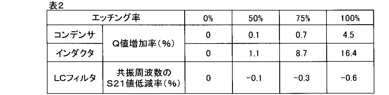
図1及び図2を参照しながら説明した配線基板1を50個製造した(エッチング率100%)。これら配線基板1について、ガラス基板10上に設けられた配線層と貫通電極との間の接続信頼性を調べた。具体的には、配線基板1の各々を熱冷衝撃試験機に取り付けて、-40℃から+125℃まで配線基板の雰囲気温度を変動させるサイクルを1000回繰り返した。その後、上記配線層と貫通電極との間の導通確認を行った。上記配線層と貫通電極との間の導通は、第1導体層20が含む配線層と第2導体層70が含む配線層との間の電気抵抗をテスターで測定することにより行った。
(例1)
図1及び図2を参照しながら説明した配線基板1を50個製造した(エッチング率100%)。ここでは、密着層72の厚さT1は60nmとし、シード層73の厚さT2は300nmとし、耐弗酸金属層21の厚さT3は50nmとした。これら配線基板1について、ガラス基板10上に設けられた配線層と貫通電極との間の導通確認を行った。上記配線層と貫通電極との間の導通は、第1導体層20が含む配線層と第2導体層70が含む配線層との間の電気抵抗をテスターで測定することにより行った。
厚さT3を100nmへ変更したこと以外は、例1において製造したのと同様の配線基板1を50個製造した。これら配線基板1についても、例1と同様の方法により、ガラス基板10上に設けられた配線層と貫通電極との間の導通確認を行った。
厚さT2を100nmへ変更し、厚さT3を50nmへ変更したこと以外は、例1において製造したのと同様の配線基板1を50個製造した。これら配線基板1についても、例1と同様の方法により、ガラス基板10上に設けられた配線層と貫通電極との間の導通確認を行った。
厚さT2を100nmへ変更し、厚さT3を100nmへ変更したこと以外は、例1において製造したのと同様の配線基板1を50個製造した。これら配線基板1についても、例1と同様の方法により、ガラス基板10上に設けられた配線層と貫通電極との間の導通確認を行った。
厚さT2を100nmへ変更し、厚さT3を200nmへ変更したこと以外は、例1において製造したのと同様の配線基板を50個製造した。これら配線基板についても、例1と同様の方法により、ガラス基板10上に設けられた配線層と貫通電極との間の導通確認を行った。
以下の表3に結果を示す。
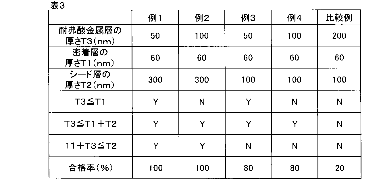
Claims (14)
- 第1面とその裏面である第2面とを有し、前記第1面から前記第2面まで各々が伸びた1以上の第1貫通孔が設けられたガラス基板と、
前記第1面と向き合った第1銅層と、前記第1銅層と前記ガラス基板との間に介在した耐弗酸金属層とを含み、前記1以上の第1貫通孔の前記第1面側の開口を覆った第1導体層であって、前記ガラス基板側の面は前記1以上の第1貫通孔の位置に凹部を有し、前記凹部の各々の開口の輪郭は、これに対応した前記第1貫通孔の前記第1面側の前記開口より大きく且つこれを取り囲んだ第1導体層と、
前記1以上の第1貫通孔の側壁、前記凹部の内面、及び前記第2面のうち前記1以上の第1貫通孔の前記第2面側の開口を取り囲んだ領域を被覆した密着層と、前記密着層上に設けられたシード層と、前記シード層上に設けられた第2銅層とを含んだ第2導体層とを備え、
前記密着層の厚さT1と前記シード層の厚さT2との合計T1+T2は、前記耐弗酸金属層の厚さT3と等しいか又はそれよりも大きい配線基板。 - 前記耐弗酸金属層には前記1以上の第1貫通孔の位置に1以上の第2貫通孔がそれぞれ設けられ、前記1以上の第2貫通孔は、前記第1導体層の前記ガラス基板側の前記面に前記凹部を形成している請求項1に記載の配線基板。
- 前記厚さT1は、前記厚さT3と等しいか又はそれよりも大きい請求項1又は2に記載の配線基板。
- 前記厚さT2は、前記厚さT1と前記厚さT3との合計T1+T3と等しいか又はそれよりも大きい請求項1乃至3の何れか1項に記載の配線基板。
- 前記厚さT2は0.5μm以下である請求項1乃至4の何れか1項に記載の配線基板。
- 前記厚さT1は10nm乃至0.5μmの範囲内にあり、前記厚さT2は100nm乃至0.5μmの範囲内にあり、前記厚さT3は10nm乃至0.5μmの範囲内にある請求項1乃至5の何れか1項に記載の配線基板。
- 前記第1導体層上に設けられた誘電体層と、前記誘電体層上に設けられた上部電極とを更に備え、前記第1導体層のうち前記上部電極と向き合った部分は下部電極であり、前記上部電極と前記誘電体層と前記下部電極とはコンデンサを構成している請求項1乃至6の何れか1項に記載の配線基板。
- 前記下部電極は、前記1以上の第1貫通孔の少なくとも1つの前記第1面側の前記開口を覆っている請求項7に記載の配線基板。
- 前記第1導体層上に設けられた誘電体層と、前記誘電体層上に設けられた上部電極とを更に備え、前記第1導体層のうち前記上部電極と向き合った部分は下部電極であり、前記上部電極と前記誘電体層と前記下部電極とはコンデンサを構成し、
前記1以上の第1貫通孔は複数の第1貫通孔であり、前記第1導体層の一部と前記第2導体層の一部とはソレノイドコイルを構成し、
前記コンデンサと前記ソレノイドコイルとはLCフィルタを構成している請求項1乃至6の何れか1項に記載の配線基板。 - インターポーザである請求項1乃至9の何れか1項に記載の配線基板。
- 第1面とその裏面である第2面とを有しているガラス基板を準備することと、
前記ガラス基板へレーザ光を照射して、前記ガラス基板に1以上の改質部を形成することと、
前記第1面上に、前記第1面と向き合った第1銅層と、前記第1銅層と前記ガラス基板との間に介在した耐弗酸金属層とを含んだ第1導体層を、前記1以上の改質部を覆うように形成することと、
弗化水素を含んだエッチング液で前記第2面をエッチングして、前記第2面を後退させるとともに、前記1以上の改質部の位置に1以上の第1貫通孔をそれぞれ形成することと、
前記耐弗酸金属層のうち前記1以上の第1貫通孔内で露出した部分をウェットエッチングに供して、前記第1導体層の前記ガラス基板側の面に凹部を形成することと、
前記1以上の第1貫通孔の側壁、前記凹部の内面、及び前記第2面を被覆した密着層を形成することと、
前記密着層上にシード層を形成することと、
前記シード層上に第2銅層を形成することと
を含み、
前記密着層と前記シード層と前記耐弗酸金属層とは、前記密着層の厚さT1と前記シード層の厚さT2との合計T1+T2が、前記耐弗酸金属層の厚さT3と等しいか又はそれよりも大きくなるように形成する配線基板の製造方法。 - 前記ガラス基板への前記レーザ光の照射に先立ち、前記ガラス基板を第1支持体に、前記第2面が前記第1支持体と向き合うように支持させることと、
前記第1導体層を形成した後であって、前記1以上の第1貫通孔を形成する前に、前記ガラス基板から前記第1支持体を除去することと
を更に含んだ請求項11に記載の配線基板の製造方法。 - 前記耐弗酸金属層への前記ウェットエッチングは、前記耐弗酸金属層に1以上の第2貫通孔が形成されるように行う請求項11又は12に記載の配線基板の製造方法。
- 前記第1導体層を形成した後であって、前記1以上の第1貫通孔を形成する前に、前記ガラス基板と前記第1導体層とを含んだ複合体を、第2支持体に、前記第1導体層が前記第2支持体と向き合うように支持させることを更に含んだ請求項11乃至13の何れか1項に記載の配線基板の製造方法。
Priority Applications (3)
| Application Number | Priority Date | Filing Date | Title |
|---|---|---|---|
| EP23867933.6A EP4593537A4 (en) | 2022-09-22 | 2023-08-16 | CABLING SUBSTRATE |
| CN202380066275.2A CN119949025A (zh) | 2022-09-22 | 2023-08-16 | 布线基板 |
| US19/079,947 US20250212324A1 (en) | 2022-09-22 | 2025-03-14 | Wiring board |
Applications Claiming Priority (2)
| Application Number | Priority Date | Filing Date | Title |
|---|---|---|---|
| JP2022151675A JP2024046350A (ja) | 2022-09-22 | 2022-09-22 | 配線基板 |
| JP2022-151675 | 2022-09-22 |
Related Child Applications (1)
| Application Number | Title | Priority Date | Filing Date |
|---|---|---|---|
| US19/079,947 Continuation US20250212324A1 (en) | 2022-09-22 | 2025-03-14 | Wiring board |
Publications (1)
| Publication Number | Publication Date |
|---|---|
| WO2024062808A1 true WO2024062808A1 (ja) | 2024-03-28 |
Family
ID=90454226
Family Applications (1)
| Application Number | Title | Priority Date | Filing Date |
|---|---|---|---|
| PCT/JP2023/029603 Ceased WO2024062808A1 (ja) | 2022-09-22 | 2023-08-16 | 配線基板 |
Country Status (6)
| Country | Link |
|---|---|
| US (1) | US20250212324A1 (ja) |
| EP (1) | EP4593537A4 (ja) |
| JP (1) | JP2024046350A (ja) |
| CN (1) | CN119949025A (ja) |
| TW (1) | TW202431908A (ja) |
| WO (1) | WO2024062808A1 (ja) |
Cited By (1)
| Publication number | Priority date | Publication date | Assignee | Title |
|---|---|---|---|---|
| CN119480848A (zh) * | 2025-01-10 | 2025-02-18 | 江苏汇显显示技术有限公司 | 芯片封装基板及其制备方法 |
Citations (6)
| Publication number | Priority date | Publication date | Assignee | Title |
|---|---|---|---|---|
| JP2015038962A (ja) * | 2013-07-16 | 2015-02-26 | ソニー株式会社 | 配線基板および配線基板の製造方法、並びに、部品内蔵ガラス基板および部品内蔵ガラス基板の製造方法。 |
| WO2019235617A1 (ja) * | 2018-06-08 | 2019-12-12 | 凸版印刷株式会社 | ガラスデバイスの製造方法、及びガラスデバイス |
| WO2021100696A1 (ja) * | 2019-11-18 | 2021-05-27 | 凸版印刷株式会社 | ガラスコア多層配線基板及びその製造方法 |
| JP2022032990A (ja) * | 2020-08-14 | 2022-02-25 | ズハイ アクセス セミコンダクター シーオー.,エルティーディー | ガラス媒体に埋め込まれた受動デバイス構造及びその製造方法 |
| JP7067666B1 (ja) * | 2021-11-30 | 2022-05-16 | 凸版印刷株式会社 | 多層配線基板の製造方法 |
| WO2022203037A1 (ja) * | 2021-03-26 | 2022-09-29 | 凸版印刷株式会社 | 配線基板の製造方法及び配線基板 |
Family Cites Families (1)
| Publication number | Priority date | Publication date | Assignee | Title |
|---|---|---|---|---|
| KR20190003025A (ko) * | 2017-06-30 | 2019-01-09 | 주식회사 에스디티아이엔씨 | 유리회로기판 및 그 제조방법 |
-
2022
- 2022-09-22 JP JP2022151675A patent/JP2024046350A/ja active Pending
-
2023
- 2023-08-16 EP EP23867933.6A patent/EP4593537A4/en active Pending
- 2023-08-16 CN CN202380066275.2A patent/CN119949025A/zh active Pending
- 2023-08-16 WO PCT/JP2023/029603 patent/WO2024062808A1/ja not_active Ceased
- 2023-09-21 TW TW112136019A patent/TW202431908A/zh unknown
-
2025
- 2025-03-14 US US19/079,947 patent/US20250212324A1/en active Pending
Patent Citations (6)
| Publication number | Priority date | Publication date | Assignee | Title |
|---|---|---|---|---|
| JP2015038962A (ja) * | 2013-07-16 | 2015-02-26 | ソニー株式会社 | 配線基板および配線基板の製造方法、並びに、部品内蔵ガラス基板および部品内蔵ガラス基板の製造方法。 |
| WO2019235617A1 (ja) * | 2018-06-08 | 2019-12-12 | 凸版印刷株式会社 | ガラスデバイスの製造方法、及びガラスデバイス |
| WO2021100696A1 (ja) * | 2019-11-18 | 2021-05-27 | 凸版印刷株式会社 | ガラスコア多層配線基板及びその製造方法 |
| JP2022032990A (ja) * | 2020-08-14 | 2022-02-25 | ズハイ アクセス セミコンダクター シーオー.,エルティーディー | ガラス媒体に埋め込まれた受動デバイス構造及びその製造方法 |
| WO2022203037A1 (ja) * | 2021-03-26 | 2022-09-29 | 凸版印刷株式会社 | 配線基板の製造方法及び配線基板 |
| JP7067666B1 (ja) * | 2021-11-30 | 2022-05-16 | 凸版印刷株式会社 | 多層配線基板の製造方法 |
Non-Patent Citations (1)
| Title |
|---|
| See also references of EP4593537A4 * |
Cited By (1)
| Publication number | Priority date | Publication date | Assignee | Title |
|---|---|---|---|---|
| CN119480848A (zh) * | 2025-01-10 | 2025-02-18 | 江苏汇显显示技术有限公司 | 芯片封装基板及其制备方法 |
Also Published As
| Publication number | Publication date |
|---|---|
| CN119949025A (zh) | 2025-05-06 |
| TW202431908A (zh) | 2024-08-01 |
| EP4593537A1 (en) | 2025-07-30 |
| JP2024046350A (ja) | 2024-04-03 |
| US20250212324A1 (en) | 2025-06-26 |
| EP4593537A4 (en) | 2026-01-14 |
Similar Documents
| Publication | Publication Date | Title |
|---|---|---|
| US11881414B2 (en) | Method for manufacturing glass device, and glass device | |
| TWI670803B (zh) | 中介層、半導體裝置、中介層的製造方法及半導體裝置的製造方法 | |
| US8324513B2 (en) | Wiring substrate and semiconductor apparatus including the wiring substrate | |
| JP6539992B2 (ja) | 配線回路基板、半導体装置、配線回路基板の製造方法、半導体装置の製造方法 | |
| JP4057589B2 (ja) | 電子部品搭載基板の製造方法 | |
| JP6840935B2 (ja) | 配線回路基板の製造方法 | |
| CN1551708B (zh) | 多层布线板 | |
| JP6672859B2 (ja) | 配線回路基板用のコア基板の製造方法、配線回路基板の製造方法、および半導体装置の製造方法 | |
| CN111328427A (zh) | 配线基板、半导体装置以及配线基板的制造方法 | |
| JP2018032657A (ja) | プリント配線板およびプリント配線板の製造方法 | |
| CN105191514A (zh) | 布线基板以及使用该布线基板的安装结构体 | |
| WO2001052322A1 (en) | Semiconductor device, metal laminated plate for fabricating circuit on semiconductor, and method of fabricating circuit | |
| US20250212324A1 (en) | Wiring board | |
| US12463056B2 (en) | Wiring board manufacturing method and wiring board | |
| JP4890959B2 (ja) | 配線基板及びその製造方法並びに半導体パッケージ | |
| JP2024083846A (ja) | 配線基板及び配線基板の製造方法 | |
| JP2022151789A (ja) | 配線基板の製造方法及び配線基板 | |
| JP2022151790A (ja) | 配線基板の製造方法及び配線基板 | |
| WO2024106066A1 (ja) | 配線基板及び配線基板の製造方法 | |
| CN119547574A (zh) | 玻璃芯层叠结构体以及玻璃芯层叠结构体的制造方法 | |
| JP6354130B2 (ja) | 両面配線基板の製造方法、両面配線基板、半導体装置 | |
| CN101287338A (zh) | 线路基板的导电盲孔的制作方法 | |
| JP7129476B2 (ja) | 積層体及びその製造方法 | |
| JP2024134681A (ja) | 配線基板および配線基板の製造方法 | |
| JP2018207036A (ja) | 部品形成基板、部品、および部品形成基板の製造方法 |
Legal Events
| Date | Code | Title | Description |
|---|---|---|---|
| 121 | Ep: the epo has been informed by wipo that ep was designated in this application |
Ref document number: 23867933 Country of ref document: EP Kind code of ref document: A1 |
|
| WWE | Wipo information: entry into national phase |
Ref document number: 202380066275.2 Country of ref document: CN |
|
| WWE | Wipo information: entry into national phase |
Ref document number: 2023867933 Country of ref document: EP |
|
| NENP | Non-entry into the national phase |
Ref country code: DE |
|
| ENP | Entry into the national phase |
Ref document number: 2023867933 Country of ref document: EP Effective date: 20250422 |
|
| WWP | Wipo information: published in national office |
Ref document number: 202380066275.2 Country of ref document: CN |
|
| WWP | Wipo information: published in national office |
Ref document number: 2023867933 Country of ref document: EP |