WO2024100947A1 - 太陽電池 - Google Patents
太陽電池 Download PDFInfo
- Publication number
- WO2024100947A1 WO2024100947A1 PCT/JP2023/029078 JP2023029078W WO2024100947A1 WO 2024100947 A1 WO2024100947 A1 WO 2024100947A1 JP 2023029078 W JP2023029078 W JP 2023029078W WO 2024100947 A1 WO2024100947 A1 WO 2024100947A1
- Authority
- WO
- WIPO (PCT)
- Prior art keywords
- solar cell
- electrode
- passivation film
- crystalline silicon
- glass frit
- Prior art date
- Legal status (The legal status is an assumption and is not a legal conclusion. Google has not performed a legal analysis and makes no representation as to the accuracy of the status listed.)
- Ceased
Links
Classifications
-
- H—ELECTRICITY
- H10—SEMICONDUCTOR DEVICES; ELECTRIC SOLID-STATE DEVICES NOT OTHERWISE PROVIDED FOR
- H10F—INORGANIC SEMICONDUCTOR DEVICES SENSITIVE TO INFRARED RADIATION, LIGHT, ELECTROMAGNETIC RADIATION OF SHORTER WAVELENGTH OR CORPUSCULAR RADIATION
- H10F77/00—Constructional details of devices covered by this subclass
- H10F77/30—Coatings
- H10F77/306—Coatings for devices having potential barriers
- H10F77/311—Coatings for devices having potential barriers for photovoltaic cells
-
- H—ELECTRICITY
- H01—ELECTRIC ELEMENTS
- H01B—CABLES; CONDUCTORS; INSULATORS; SELECTION OF MATERIALS FOR THEIR CONDUCTIVE, INSULATING OR DIELECTRIC PROPERTIES
- H01B1/00—Conductors or conductive bodies characterised by the conductive materials; Selection of materials as conductors
- H01B1/20—Conductive material dispersed in non-conductive organic material
- H01B1/22—Conductive material dispersed in non-conductive organic material the conductive material comprising metals or alloys
-
- H—ELECTRICITY
- H10—SEMICONDUCTOR DEVICES; ELECTRIC SOLID-STATE DEVICES NOT OTHERWISE PROVIDED FOR
- H10F—INORGANIC SEMICONDUCTOR DEVICES SENSITIVE TO INFRARED RADIATION, LIGHT, ELECTROMAGNETIC RADIATION OF SHORTER WAVELENGTH OR CORPUSCULAR RADIATION
- H10F10/00—Individual photovoltaic cells, e.g. solar cells
- H10F10/10—Individual photovoltaic cells, e.g. solar cells having potential barriers
- H10F10/14—Photovoltaic cells having only PN homojunction potential barriers
-
- H—ELECTRICITY
- H10—SEMICONDUCTOR DEVICES; ELECTRIC SOLID-STATE DEVICES NOT OTHERWISE PROVIDED FOR
- H10F—INORGANIC SEMICONDUCTOR DEVICES SENSITIVE TO INFRARED RADIATION, LIGHT, ELECTROMAGNETIC RADIATION OF SHORTER WAVELENGTH OR CORPUSCULAR RADIATION
- H10F77/00—Constructional details of devices covered by this subclass
- H10F77/20—Electrodes
-
- H—ELECTRICITY
- H10—SEMICONDUCTOR DEVICES; ELECTRIC SOLID-STATE DEVICES NOT OTHERWISE PROVIDED FOR
- H10F—INORGANIC SEMICONDUCTOR DEVICES SENSITIVE TO INFRARED RADIATION, LIGHT, ELECTROMAGNETIC RADIATION OF SHORTER WAVELENGTH OR CORPUSCULAR RADIATION
- H10F77/00—Constructional details of devices covered by this subclass
- H10F77/20—Electrodes
- H10F77/206—Electrodes for devices having potential barriers
- H10F77/211—Electrodes for devices having potential barriers for photovoltaic cells
Definitions
- the present invention relates to a crystalline silicon solar cell that uses a crystalline silicon substrate.
- Semiconductor devices such as crystalline silicon solar cells that use crystalline silicon, which is made by processing single crystal silicon or polycrystalline silicon into a flat plate, as a substrate generally have electrodes formed on the surface of the silicon substrate using a conductive paste for electrode formation in order to make electrical contact with the outside of the device.
- electrodes are formed in this way, the production volume of crystalline silicon solar cells has increased significantly in recent years.
- These solar cells have an impurity diffusion layer, an anti-reflective film (passivation film), and a light-incident surface electrode on one surface of the crystalline silicon substrate, and a back electrode on the other surface.
- the light-incident surface electrode and back electrode allow the electricity generated by the crystalline silicon solar cell to be extracted to the outside.
- Electrodes for crystalline silicon solar cells are formed using a conductive paste that contains conductive powder, glass frit, organic binder, solvent and other additives.
- Silver particles are mainly used as the conductive powder.
- Patent Document 1 describes a method for manufacturing a crystalline silicon solar cell.
- Patent Document 1 describes the use of a conductive paste for forming electrodes that contains an inorganic material to form electrodes for crystalline silicon solar cells.
- Patent Document 1 describes that the inorganic material is composed of conductive particles and glass frit.
- Patent document 2 describes a process for improving the ohmic contact behavior between a contact grid and an emitter layer in a silicon solar cell. Specifically, the process described in patent document 2 involves applying a predetermined voltage in the forward and reverse directions of the silicon solar cell, guiding a point light source to the solar surface side of the silicon solar cell, thereby irradiating a cross section of a subsection on the solar surface side.
- Patent Document 3 describes a conductive composition for forming an electrode for a solar cell, which contains silver powder, glass powder containing PbO, and a vehicle made of an organic substance.
- the conductive composition is a conductive composition for forming an electrode that penetrates a silicon nitride layer and is conductive with an n-type semiconductor layer formed below the silicon nitride layer.
- Patent Document 3 also describes that the basicity of the glass powder contained in the conductive composition is 0.6 to 0.8, and that the glass transition point is 300°C to 450°C.
- FIG. 5 shows an example of a schematic cross-sectional view of a typical crystalline silicon solar cell.
- the electrode pattern of the light-incident surface electrode 20 (surface electrode) is printed on the passivation film 2 that functions as the passivation film 2 using a conductive paste by screen printing or the like, the conductive paste is dried, and the light-incident surface electrode 20 is formed by baking at a predetermined temperature.
- the conductive paste fires through the passivation film 2 during baking at this predetermined temperature. This fire-through allows the light-incident surface electrode 20 to be formed so as to be in contact with the impurity diffusion layer 4.
- the fire-through refers to etching the passivation film 2, which is an insulating film, with glass frit or the like contained in the conductive paste to electrically connect the light-incident surface electrode 20 and the impurity diffusion layer 4.
- the electrode pattern when the electrode pattern is baked, the electrode pattern fires through the passivation film 2, causing the passivation film 2 to disappear, and the light-incident surface electrode 20 and the impurity diffusion layer 4 are in contact.
- a pn junction is formed at the interface between the n-type crystalline silicon substrate 1 and the impurity diffusion layer 4. Most of the light incident on the crystalline silicon solar cell passes through the passivation film 2 and the impurity diffusion layer 4 and enters the n-type crystalline silicon substrate 1.
- FIG 2 shows an example of a schematic diagram of the light incident surface of a crystalline silicon solar cell.
- a busbar electrode (light incident busbar electrode 20a) and a light incident finger electrode 20b (sometimes simply referred to as “finger electrode 20b") are arranged on the light incident surface of the crystalline silicon solar cell as the light incident surface electrode 20.
- the electrons of the electron-hole pairs generated by the incident light entering the crystalline silicon solar cell are collected by the finger electrode 20b and are further collected by the light incident busbar electrode 20a.
- a metal ribbon for interconnection, surrounded by solder, is soldered to the light incident busbar electrode 20a, and current is taken out to the outside by this metal ribbon.
- the light-to-electricity conversion efficiency of a solar cell (sometimes simply called “conversion efficiency") is expressed as the product of the fill factor (FF), open circuit voltage (Voc), and short circuit current (Jsc). Essentially, there is a trade-off between the fill factor (FF) and the open circuit voltage (Voc), and it is difficult to simultaneously increase both the fill factor and the open circuit voltage.
- the present invention aims to provide a highly efficient crystalline silicon solar cell with a high open circuit voltage (Voc) and fill factor (FF).
- the present invention aims to provide a crystalline silicon solar cell in which the space between the electrode and the substrate has a predetermined structure in order to obtain a highly efficient crystalline silicon solar cell with a high open circuit voltage (Voc) and fill factor (FF).
- the present invention has the following configuration.
- a first aspect of the present invention provides a substrate including a crystalline silicon, the substrate including an impurity diffusion layer on at least one surface thereof; a passivation film disposed on at least a portion of the impurity diffusion layer of the substrate; an electrode comprising silver (Ag), the electrode being disposed on at least a portion of the passivation film; the solar cell further includes at least one AgSi region disposed at least partially between the electrode and the substrate; The AgSi region includes at least one AgSi region having a depth of 100 nm or more; In a scanning electron microscope photograph of a 5.7 ⁇ m ⁇ 3.9 ⁇ m cross section including the AgSi region of the solar cell, the remaining rate of the passivation film, which is the ratio of the length over which the passivation film remains, is 10 to 90%.
- Configuration 2 is the solar cell of Configuration 1, in which the ratio Db/Da of the thickness Da of the passivation film immediately after deposition to the thickness Db of the passivation film in a scanning electron microscope photograph of a 5.7 ⁇ m ⁇ 3.9 ⁇ m cross section including the AgSi region of the solar cell completed by forming the electrodes on the surface of the solar cell is 15% to 85%.
- Configuration 3 is the solar cell of Configuration 1 or 2, wherein the electrode further comprises 0.1 to 5.0 parts by weight of glass frit per 100 parts by weight of the silver (Ag) contained in the electrode.
- Configuration 4 is the solar cell of Configuration 3, wherein the glass frit has a glass transition point of 250 to 600°C.
- Configuration 5 is the solar cell of configuration 3 or 4, wherein the glass frit comprises at least one selected from SiO2, B2O3, V2O5, Bi2O3 , TeO2 , Li2O , and ZnO .
- Configuration 6 is the solar cell of any one of Configurations 3 to 5, wherein the glass frit is substantially free of PbO.
- a seventh aspect of the present invention is the solar cell of any one of claims 1 to 6, wherein the electrodes are substantially free of lead (Pb).
- Configuration 8 is the solar cell of any of Configurations 1-7, wherein the electrode is substantially free of aluminum particles.
- Aspect 9 is a crystalline silicon substrate of a first conductivity type; the impurity diffusion layer is a second conductivity type impurity diffusion layer,
- the electrode is a light-incident surface electrode disposed on the light-incident surface,
- the solar cell further includes a back electrode arranged to be electrically connected to a surface of the crystalline silicon substrate opposite to the light incident surface,
- the solar cell of any of configurations 1 to 8, wherein the light incident side surface electrode is a light incident side surface electrode that has been treated to irradiate the light incident side surface of the solar cell with light from a point light source while applying a voltage between the back electrode and the light incident side surface electrode so that a current flows in a direction opposite to a forward current between the impurity diffusion layer of the second conductivity type and the crystalline silicon substrate of the first conductivity type.
- the present invention it is possible to provide a highly efficient crystalline silicon solar cell having a high open circuit voltage (Voc) and fill factor (FF).
- a crystalline silicon solar cell having a predetermined structure between the electrode and the substrate in order to obtain a highly efficient crystalline silicon solar cell having a high open circuit voltage (Voc) and fill factor (FF).
- FIG. 1 is an example of a schematic cross-sectional view of a crystalline silicon solar cell according to an embodiment of the present invention.
- 1 is a schematic diagram of an example of the light incident surface of a crystalline silicon solar cell.
- 1 is an example of a schematic diagram of the back surface of a crystalline silicon solar cell.
- 1 is an example of a schematic cross-sectional view of a bifacial crystalline silicon solar cell according to an embodiment of the present invention.
- FIG. 1 is an example of a schematic cross-sectional view of a typical crystalline silicon solar cell near the light-incident surface electrode (finger electrode), showing that the anti-reflection film (passivation film) between the electrode and the impurity diffusion layer has disappeared due to fire-through.
- FIG. 1 is an example of a schematic cross-sectional view of a typical crystalline silicon solar cell near the light-incident surface electrode (finger electrode), showing that the anti-reflection film (passivation film) between the electrode and the impurity
- FIG. 11 is a cross-sectional SEM (scanning electron microscope) photograph (magnification: 20,000 times) of the crystalline silicon solar cell of Example 3 near the passivation film on the light-incident surface, illustrating the depth d of the AgSi region.
- This is a cross-sectional SEM (scanning electron microscope) photograph (magnification: 20,000 times) of the crystalline silicon solar cell of Example 3 near the passivation film on the light-incident surface, and is a figure for explaining the passivation film residual rate Lp/(Lp+Le).
- 1 is a cross-sectional SEM (scanning electron microscope) photograph (magnification: 20,000 times) of the crystalline silicon solar cell of Comparative Example 1 near the passivation film on the light incident surface.
- the solar cell of this embodiment includes a substrate (crystalline silicon substrate 1) containing crystalline silicon, a passivation film 2, and an electrode (e.g., a light-incident surface electrode 20).
- the solar cell of this embodiment further includes at least one AgSi region 30 disposed at least partially between the electrode and the substrate.
- the solar cell of this embodiment includes a substrate.
- the substrate of the solar cell of this embodiment is a crystalline silicon substrate 1. Therefore, the solar cell of this embodiment is a crystalline silicon solar cell.
- crystalline silicon includes single crystal and polycrystalline silicon.
- crystalline silicon substrate refers to a material in which crystalline silicon is formed into a shape suitable for forming elements, such as a flat plate, in order to form semiconductor devices such as electric or electronic elements. Any method may be used to manufacture crystalline silicon. For example, the Czochralski method can be used for single crystal silicon, and the casting method can be used for polycrystalline silicon. Other manufacturing methods, such as polycrystalline silicon ribbons manufactured by the ribbon pulling method, and polycrystalline silicon formed on a heterogeneous substrate such as glass, can also be used as the crystalline silicon substrate 1.
- crystalline silicon solar cell refers to a solar cell manufactured using the crystalline silicon substrate 1. In this specification, the crystalline silicon substrate 1 may be simply referred to as the "substrate”.
- crystalline silicon, silicon carbide, germanium, gallium arsenide, etc. can be used as the material for the semiconductor substrate of the solar cell. From the standpoint of safety and cost as a solar cell, it is preferable that the material for the semiconductor substrate is crystalline silicon (single crystal silicon, polycrystalline silicon, etc.).
- the crystalline silicon substrate 1 of the solar cell of this embodiment is an n-type crystalline silicon substrate 1 or a p-type crystalline silicon substrate 1 containing n-type or p-type impurities.
- n-type impurities contained in the n-type crystalline silicon substrate 1 include Group 13 elements such as boron (B), aluminum (Al), and gallium (Ga).
- p-type impurities contained in the p-type crystalline silicon substrate 1 include Group 15 elements such as phosphorus (P), arsenic (As), and antimony (Sb).
- the solar cell of this embodiment includes an impurity diffusion layer 4 on at least a portion of at least one surface of a crystalline silicon substrate 1.
- the impurity diffusion layer 4 formed on the light-incident surface is a p-type or n-type impurity diffusion layer 4.
- the portion of the substrate where the impurity diffusion layer 4 is not formed, as shown in FIG. 1, may be referred to as the "substrate body 6.”
- the impurity diffusion layer 4 is of the second conductivity type.
- the impurity diffusion layer 4 formed on at least one surface of the crystalline silicon substrate 1 is a p-type impurity diffusion layer 4.
- the impurity diffusion layer 4 formed on at least one surface of the crystalline silicon substrate 1 is an n-type impurity diffusion layer 4.
- the first conductivity type crystalline silicon substrate 1 of the solar cell of this embodiment is preferably an n-type crystalline silicon substrate 1.
- the second conductivity type impurity diffusion layer 4 of the solar cell of this embodiment is preferably a p-type impurity diffusion layer 4.
- the mobility of electrons, which are carriers in an n-type crystalline silicon substrate 1 is higher than the mobility of holes, which are carriers in a p-type crystalline silicon substrate 1. Therefore, in order to obtain a solar cell with high conversion efficiency, it is advantageous to use an n-type crystalline silicon substrate 1.
- the sheet resistance of the impurity diffusion layer 4 is preferably 30 to 300 ⁇ / ⁇ (square), 40 to 160 ⁇ / ⁇ (square), and more preferably 45 to 120 ⁇ / ⁇ .
- the depth to which the impurity diffusion layer 4 is formed can be 0.3 ⁇ m to 1.0 ⁇ m.
- the depth of the impurity diffusion layer 4 refers to the depth from the surface of the impurity diffusion layer 4 to the pn junction.
- the depth of the pn junction can be the depth from the surface of the impurity diffusion layer 4 to the point where the impurity concentration in the impurity diffusion layer 4 is approximately the same as the impurity concentration in the substrate body 6.
- the impurity diffusion layer 4 of the crystalline silicon solar cell of this embodiment may be referred to as the "silicon emitter layer.”
- the solar cell of this embodiment includes a passivation film 2.
- the passivation film 2 is disposed on at least a portion of the impurity diffusion layer 4 of the substrate.
- the passivation film 2 can function as an anti-reflection film.
- the passivation film 2 formed on the light-incident surface of the crystalline silicon substrate 1 may be referred to as an anti-reflection film.
- the passivation film 2 can be a film consisting of a single layer or multiple layers.
- the passivation film 2 is a single layer, it is preferably a thin film (SiN film) made of silicon nitride (SiN) because it can effectively passivate the surface of the silicon substrate.
- the passivation film 2 is a multiple layer, it can be a laminated film (SiN/SiO x film) of a thin film made of silicon nitride and a thin film made of silicon oxide.
- the passivation film 2 is a SiN/SiO x film
- the SiO x film can be a natural oxide film of the silicon substrate.
- Figure 5 shows an example of a schematic cross-sectional view of a typical crystalline silicon solar cell.
- a passivation film 2 anti-reflection film
- an electrode pattern of the light-incident surface electrode 20 is printed on the passivation film 2 using a conductive paste by screen printing or the like, and the conductive paste is dried and baked at a predetermined temperature to form the light-incident surface electrode 20.
- the conductive paste fires through the passivation film 2 during baking at this predetermined temperature.
- this fire-through allows the light-incident surface electrode 20 to be formed so as to be in electrical contact with the impurity diffusion layer 4.
- fire-through refers to etching the passivation film 2, which is an insulating film, with glass frit or the like contained in the conductive paste to electrically connect the light-incident surface electrode 20 and the impurity diffusion layer 4.
- the electrode pattern fires through the passivation film 2, causing the passivation film 2 to disappear and expose the light-incident surface electrode 20 to the impurity diffusion layer 4.
- the passivation film 2 (anti-reflection film) is present in most of the area between the light-incident surface electrode 20 and the impurity diffusion layer 4. Therefore, in the case of the crystalline silicon solar cell of this embodiment, the passivation film 2 in the portion in contact with the impurity diffusion layer 4 of the crystalline silicon substrate 1 can remain mostly intact in the portion other than the AgSi region 30 described below. The presence of the passivation film 2 can prevent an increase in the surface defect density that causes carrier recombination. As a result, the crystalline silicon solar cell of this embodiment can obtain a high open circuit voltage (Voc).
- Voc open circuit voltage
- the degree to which the passivation film 2 remains between the electrode and the crystalline silicon substrate 1 after firing to form the electrode is indicated as the remaining rate of the passivation film 2. The remaining rate of the passivation film 2 will be described later.
- the solar cell of this embodiment includes an electrode.
- the electrode of the solar cell of this embodiment is disposed on at least a portion of the passivation film 2.
- the electrode of the solar cell of this embodiment includes silver (Ag).
- finger electrodes 20b are arranged on the light incident surface of the crystalline silicon solar cell as light incident surface electrodes 20.
- the holes of electron-hole pairs generated by incident light entering the crystalline silicon solar cell are collected in finger electrode 20b via impurity diffusion layer 4 (e.g., p-type impurity diffusion layer 4). Therefore, low contact resistance is required between finger electrode 20b and impurity diffusion layer 4.
- a back electrode 15 is disposed on the back surface opposite to the light incident surface of the crystalline silicon solar cell shown in FIG. 1.
- the light incident surface electrode 20 and the back electrode 15, which are electrodes for extracting current from the crystalline silicon solar cell to the outside, may be simply referred to as "electrodes”.
- FIG. 4 shows an example of a cross-sectional schematic diagram of a bifacial crystalline silicon solar cell (bifacial power generation crystalline silicon solar cell) of this embodiment.
- the crystalline silicon solar cell shown in FIG. 4 can generate power by receiving light from two surfaces (first and second light incident surfaces).
- the electrodes of crystalline silicon solar cells can be formed by printing a conductive paste by a method such as screen printing and firing.
- the conductive paste for forming the electrodes of the crystalline silicon solar cells of this embodiment may be referred to as a specified conductive paste.
- the conductive paste contains conductive particles and an organic vehicle.
- the conductive paste may further contain glass frit in addition to the conductive particles and the organic vehicle.
- the electrodes of the solar cells of this embodiment contain silver (Ag). Therefore, the conductive particles contained in the specified conductive paste must contain silver (Ag).
- the organic vehicle contained in the conductive paste is burned away during firing to form the electrodes. Therefore, the electrodes after firing contain components contained in the conductive paste other than the organic vehicle. Specifically, the electrodes after firing contain conductive components resulting from the conductive particles of the conductive paste. In addition, when the conductive paste contains glass frit, the electrodes after firing further contain components resulting from the glass frit of the conductive paste.
- the conductive component contained in a specific electrode of the crystalline silicon solar cell of this embodiment consists of only silver. Note that a conductive component consisting of only silver may contain other metal elements as unavoidable impurities.
- glass frit is made primarily of multiple types of oxides, such as metal oxides, and is generally used in the form of glass-like particles. When fired to form an electrode, the glass frit softens and the particles bond together.
- the components (oxides) originating from the glass frit contained in the electrode are also simply referred to as "glass frit.”
- the content of glass frit contained in the electrode is preferably 0.1 to 5.0 parts by weight, more preferably 0.2 to 4.0 parts by weight, even more preferably 0.3 to 3.0 parts by weight, and particularly preferably 0.4 to 2.7 parts by weight, per 100 parts by weight of silver (Ag) contained in the electrode.
- the glass transition point of the glass frit contained in the electrode is preferably 250 to 600°C, more preferably 270 to 500°C, and even more preferably 300 to 400°C.
- the glass transition point (Tg) of the glass frit 250°C or higher, it is possible to suppress reactivity with the passivation film 2.
- the glass transition point (Tg) 600°C or lower it is possible to reduce the contact resistance between the resulting electrode (for example, the light-incident surface electrode 20) and the impurity diffusion layer 4.
- the glass frit contained in the electrode preferably contains at least one selected from SiO 2 , B 2 O 3 , V 2 O 5 , Bi 2 O 3 , TeO 2 , BaO, CuO, Li 2 O and ZnO.
- the glass frit contained in the electrode more preferably contains at least one selected from SiO 2 , B 2 O 3 , V 2 O 5 , Bi 2 O 3 , TeO 2 , Li 2 O and ZnO.
- the solar cell of this embodiment may have a glass frit contained in the electrode that is substantially free of PbO.
- the electrode of the solar cell of this embodiment may have a glass frit that is substantially free of lead (Pb).
- lead-free glass frit means glass frit that is substantially free of lead (Pb). Since glass frit is manufactured using metal oxide as a raw material, lead-free glass frit means glass frit that is substantially free of lead oxide (PbO).
- lead-free glass frit may contain a small amount of lead that is inevitably mixed in as an impurity. Specifically, the lead-free glass frit of this embodiment may contain 0.1 wt % or less of lead as an impurity relative to 100 wt % of glass frit.
- a glass frit containing lead oxide (PbO) (lead-containing glass frit) is used as the glass frit contained in the conductive paste for forming the electrodes.
- the conductive paste for forming the electrodes contains a lead-containing glass frit, which can reduce the contact resistance between the light-incident surface electrode 20 and the impurity diffusion layer 4.
- lead has adverse effects on the human body.
- a product is manufactured using a material containing lead, there is a risk that the lead will pollute the environment when the product is disposed of. Therefore, it is desirable to use lead-free materials that do not contain lead when manufacturing products.
- lead-free glass frit in the manufacturing process of the solar cell.
- a solar cell having an electrode that does not substantially contain lead (Pb) can be manufactured. Therefore, environmental pollution by lead can be suppressed.
- the crystalline silicon solar cell of this embodiment can be made so that materials other than the electrodes also contain substantially no lead. In order to prevent environmental pollution by lead, it is preferable that the crystalline silicon solar cell of this embodiment is a lead-free solar cell.
- the electrode of the solar cell of this embodiment may further contain an aluminum component resulting from aluminum particles.
- the aluminum particles may be contained as particles separate from the (A) conductive particles. If the conductive paste for forming the electrode contains aluminum, the electrode will also contain aluminum.
- aluminum has the properties of a p-type impurity.
- the conductive paste printed on the crystalline silicon is fired, the aluminum in the conductive paste diffuses into the crystalline silicon and becomes a p-type impurity. Therefore, when forming an electrode on the surface of the p-type semiconductor layer of the crystalline silicon substrate 1, the conductive paste can contain aluminum particles, thereby making it possible to obtain low contact resistance between the electrode and the p-type semiconductor layer. Therefore, when forming an electrode on the surface of the p-type semiconductor layer of the crystalline silicon substrate 1, the conductive paste can contain aluminum particles.
- the adhesion of the electrode to the p-type semiconductor layer may decrease, causing the electrode to easily peel off from the p-type semiconductor layer of the solar cell.
- the conductive paste contains aluminum particles, the reliability of the electrode with respect to the p-type semiconductor layer will be significantly impaired.
- metal ribbons for interconnection are soldered to the electrodes of the solar cells. If the conductive paste used to form the electrodes contains aluminum particles, there is a problem in that the soldering strength of the metal ribbon to the electrodes decreases.
- the conductive paste of this embodiment contains no more than a specified amount of aluminum particles, or does not contain any aluminum particles.
- the conductive paste of this embodiment further contains 0.5 parts by weight or less of aluminum particles per 100 parts by weight of (A) silver particles, or does not contain aluminum particles.
- the upper limit of the content of aluminum particles in the conductive paste of this embodiment is preferably 0.3 parts by weight or less per 100 parts by weight of (A) silver particles, more preferably less than 0.3 parts by weight, and even more preferably 0.25 parts by weight or less.
- the conductive paste of this embodiment can be a conductive paste that does not contain aluminum particles. Note that "does not contain aluminum particles” means that "aluminum particles" are not intentionally added, and does not exclude the inclusion of aluminum components as an unavoidable impurity.
- At least one AgSi region is formed at least partially between the electrode and the substrate, so that when an electrode is formed on the surface of the p-type semiconductor layer of the crystalline silicon substrate 1, low contact resistance can be obtained between the electrode and the p-type semiconductor layer even if the electrode does not substantially contain aluminum.
- the conductive paste used to form the electrodes contains aluminum, this can have an impact on reliability.
- the electrodes of the crystalline silicon solar cell may include a light incident busbar electrode 20a and/or a back TAB electrode 15a.
- the light incident busbar electrode 20a has a function of electrically connecting the finger electrode 20b for collecting the current generated by the solar cell and the metal ribbon for interconnection.
- the back TAB electrode 15a has a function of electrically connecting the entire back electrode 15b for collecting the current generated by the solar cell and the metal ribbon for interconnection. If the finger electrode 20b comes into contact with the crystalline silicon substrate 1, the surface defect density of the surface (interface) of the crystalline silicon substrate 1 where the finger electrode 20b comes into contact increases, and the solar cell performance decreases.
- the passivation film 2 (anti-reflection film) is not completely fired through when the finger electrode 20b is formed. Therefore, most of the passivation film 2 in the part in contact with the crystalline silicon substrate 1 can be kept in its original state, and an increase in the surface defect density that causes carrier recombination can be prevented. As a result, a crystalline silicon solar cell with a high open circuit voltage (Voc) can be obtained.
- the crystalline silicon solar cell shown in FIG. 1 can have a back electrode 15 with the structure shown in FIG. 3.
- the back electrode 15 is arranged so as to be electrically connected to the other surface of the semiconductor substrate of the first conductivity type.
- the back electrode 15 can generally include a full back electrode 15b and a back TAB electrode 15a electrically connected to the full back electrode 15b.
- the busbar electrodes of the crystalline silicon solar cell shown in FIG. 1 include the light incident side busbar electrode 20a shown in FIG. 2 and the backside TAB electrode 15a as shown in FIG. 3.
- a metal ribbon for interconnection is soldered to the light incident side busbar electrode 20a and the backside TAB electrode 15a. This metal ribbon allows the current generated by the solar cell to be taken out of the crystalline silicon solar cell.
- the bifacial crystalline silicon solar cell shown in FIG. 4 can also have the light incident side busbar electrode 20a and the backside TAB electrode 15a having the same shape as the light incident side busbar electrode 20a.
- the width of the busbar electrodes (light incident side busbar electrode 20a and backside TAB electrode 15a) can be approximately the same as the width of the metal ribbon for interconnection. In order for the busbar electrodes to have low electrical resistance, the wider the width, the better. On the other hand, in order to increase the area of incidence of light on the light incident side surface, the narrower the width of the light incident side busbar electrode 20a is. Therefore, the busbar electrode width can be 0.05 to 5 mm, preferably 0.08 to 3 mm, more preferably 0.1 to 2 mm, and even more preferably 0.15 to 1 mm. In addition, the number of busbar electrodes can be determined according to the size of the crystalline silicon solar cell. The number of busbar electrodes is arbitrary.
- the number of busbar electrodes can be three or four, or more.
- the optimal number of busbar electrodes can be determined so as to maximize the conversion efficiency of the crystalline silicon solar cell by simulating the operation of the solar cell. Since the crystalline silicon solar cells are connected in series to each other by metal ribbons for interconnection, it is preferable that the number of light-incident side busbar electrodes 20a and the back TAB electrodes 15a are the same. For the same reason, it is preferable that the widths of the light-incident side busbar electrodes 20a and the back TAB electrodes 15a are the same.
- the finger electrodes 20b on the light incident surface are as narrow as possible and that there are as few of them as possible.
- the finger electrodes 20b are wide and there are many of them.
- the finger electrodes 20b are wide.
- the number of busbar electrodes can be determined according to the size of the crystalline silicon solar cell and the width of the busbar electrodes.
- the optimal width and number of finger electrodes 20b (the spacing between the finger electrodes 20b) can be determined by simulating the operation of the solar cell so as to maximize the conversion efficiency of the crystalline silicon solar cell.
- the width and number of back finger electrodes 15c of the back electrode 15 of the bifacial crystalline silicon solar cell shown in FIG. 4 can also be determined in a similar manner.
- the solar cell of this embodiment includes at least one AgSi region 30.
- the AgSi region 30 is disposed at least partially between the electrode and the substrate.
- An example of the AgSi region 30 is shown in the SEM photograph of Fig. 6.
- the AgSi region 30 may be disposed at least partially between the electrode and the substrate, and for example, the region indicated by the reference symbol 30 surrounded by a dotted line in the SEM photograph of Fig. 6 can also be the AgSi region 30.
- the silver (Ag) contained in the electrode diffuses into the silicon (Si) of the substrate, thereby forming a region of an alloy of silver (Ag) and silicon (Si) at least partially between the electrode and the substrate.
- the region of the alloy of silver (Ag) and silicon (Si) formed when manufacturing the solar cell of this embodiment is referred to as the "AgSi region 30."
- the AgSi region 30 can be identified as a region where both Ag and Si are detected when a cross section of the solar cell of this embodiment is measured with an energy dispersive X-ray fluorescence spectrometer (hereinafter sometimes referred to as EDX).
- One AgSi region 30 means an AgSi region 30 that is separated from other AgSi regions 30.
- the SEM photograph in FIG. 6 shows one AgSi region 30.
- the solar cell of this embodiment preferably has multiple spot-like AgSi regions 30 at least partially between the electrode and the substrate.
- the AgSi region 30 contributes to electrical conduction between the electrode and the impurity diffusion layer 4 as a local conductive portion.
- the portion in which the AgSi regions 30 exist is an extremely small portion of the area in which the electrode is formed.
- the crystalline silicon solar cell of this embodiment includes at least one AgSi region 30 with a depth d of 100 nm or more.
- the depth d of the AgSi region 30 refers to the length of the longest line segment (length d of the line segment connecting B1 and B2 in FIG. 6) among the line segments connecting any one point (B1 in FIG. 6) at the interface between the electrode and the AgSi region 30 to any one point (B2 in FIG. 6) at the interface between the substrate and the AgSi region 30 in an SEM photograph of a cross section of the AgSi region 30 observed with an SEM as shown in FIG. 6.
- the depth d of the AgSi region 30 can be obtained by superimposing the AgSi region 30 determined in the EDX measurement on an SEM photograph of a cross section near the passivation film 2 observed with an SEM at a magnification of 20,000 times, determining the above-mentioned predetermined line segment, and measuring the length of the predetermined line segment.
- the depth d of the AgSi region 30 is preferably 100 to 4000 nm, more preferably 120 to 3000 nm, even more preferably 130 to 2500 nm, and particularly preferably 150 to 2000 nm.
- the AgSi region 30 is preferably formed by performing a laser treatment process.
- the laser treatment process refers to a process in which light from a point light source is irradiated onto the light incident surface of the solar cell while applying a voltage between the back electrode 15b and the light incident surface electrode 20 so that a current flows in the opposite direction to the forward direction between the impurity diffusion layer 4 of the second conductivity type and the crystalline silicon substrate 1 of the first conductivity type with respect to the light incident surface electrode 20.
- the solar cell further includes a back electrode 15b arranged so as to be electrically connected to the surface of the crystalline silicon substrate 1 opposite to the light incident surface.
- the laser treatment process can form an appropriate AgSi region 30.
- the laser treatment process will be described in more detail below.
- Figure 4 shows an example of a cross-sectional schematic diagram of a bifacial crystalline silicon solar cell.
- the bifacial crystalline silicon solar cell shown in Figure 4 has an impurity diffusion layer 4, a passivation film 2 (anti-reflection film), and a back surface passivation film 14.
- the specified structure of the electrode including the AgSi region 30 can also be suitably applied as the structure of the back surface electrode 15 (back surface finger electrode 15c) of a bifacial crystalline silicon solar cell, as shown in Figure 4.
- a specified AgSi region 30 can be formed both near the light incident side surface and near the back surface.
- the extent to which the passivation film 2 exists between the electrode and the impurity diffusion layer 4 of the crystalline silicon substrate 1 after firing to form the electrode of the solar cell of this embodiment can be indicated as the remaining rate of the passivation film 2.
- the passivation film 2 disappears in the portion where the AgSi region 30 is formed. Since the AgSi region 30 is not formed in the portion where the passivation film 2 exists, the remaining rate of the passivation film 2 is considered to be the proportion of the region in the vicinity of the AgSi region 30 where the AgSi region 30 is not formed.
- the method for measuring the residual rate of the passivation film 2 will be described using an example of an SEM photograph of a cross section of a solar cell shown in Figure 7.
- a SEM photograph is obtained by observing the cross section including the passivation film 2 and the AgSi region 30 with an SEM at a magnification of 20,000 times.
- the horizontal length (horizontal to the substrate surface) of this SEM photograph is 5.7 ⁇ m, and the vertical length (perpendicular to the substrate surface) is 3.9 ⁇ m.
- the total length Lp of the cross section of the passivation film 2 in this SEM photograph is measured.
- the total length Lp of the cross section of the passivation film 2 in the SEM photograph is the total length of Lp1, Lp2, Lp3, and Lp4.
- the length Le corresponds to the length of the passivation film 2 that has disappeared during the manufacturing process of the solar cell.
- the total length Le of the cross section of the interface between the AgSi region 30 and the electrode in the portion where the AgSi region 30 is generated is the total length of Le1 and Le2.
- the remaining rate of the passivation film 2 can be obtained as Lp/(Lp+Le).
- the portion where the passivation film 2 has disappeared during the manufacturing process of the solar cell can be identified by measurement using EDX.
- the length of Le1, etc. can be measured by approximating the passivation film 2, etc. as a straight line.
- the remaining rate of the passivation film 2 is 10-90%, preferably 30% or more and less than 90%, more preferably 50% or more and less than 90%, and even more preferably 70% to 89%.
- a highly efficient crystalline silicon solar cell with a high open circuit voltage (Voc) and fill factor (FF) can be obtained.
- the film thickness ratio before and after firing of the passivation film 2 is the ratio (Db/Da) of the film thickness Da before firing for electrode formation of the passivation film 2 to the film thickness Db after firing for electrode formation (after the solar cell is completed).
- the film thickness ratio before and after firing may be simply referred to as the "film thickness ratio (Db/Da)."
- the film thickness ratio (Db/Da) is preferably 15% to 85%, more preferably 20% to 70%, and even more preferably 30% to 60%.
- the pre-firing thickness Da of the passivation film 2 refers to the thickness of the passivation film 2 when the passivation film 2 is formed on a specified substrate.
- the thickness Da immediately after film formation can be measured by SEM observation of the cross section near the passivation film 2 before forming the electrodes.
- the film thickness Db after the solar cell is completed is the film thickness of the passivation film 2 in a scanning electron microscope photograph of a 5.7 ⁇ m ⁇ 3.9 ⁇ m cross section including the AgSi region 30 of a solar cell completed by forming electrodes on the surface of the solar cell by firing.
- the film thickness Db of the passivation film 2 in a scanning electron microscope photograph of a 5.7 ⁇ m ⁇ 3.9 ⁇ m cross section including the AgSi region 30 of a solar cell completed by forming electrodes on the surface of the solar cell refers to the film thickness of the passivation film 2 near the AgSi region 30 of a solar cell completed by forming an electrode pattern using a predetermined conductive paste on the passivation film 2 formed on a predetermined substrate, and forming the electrodes and AgSi region 30 by performing a predetermined treatment such as a predetermined baking.
- the film thickness Db is sometimes referred to as the "film thickness Db after the solar cell is completed.”
- the film thickness Db after the solar cell is completed can be measured by SEM observation of the image range of 5.7 ⁇ m ⁇ 3.9 ⁇ m of the cross section including the passivation film 2 and AgSi region 30 of the solar cell completed by forming the electrodes and AgSi region 30.
- the film thickness Db after the solar cell is completed is the film thickness Db of the passivation film 2 in a scanning electron microscope photograph of a 5.7 ⁇ m ⁇ 3.9 ⁇ m cross section including the AgSi region 30 of the completed solar cell.
- the thickness Db of the passivation film 2 after the solar cell is completed can be obtained by observing the cross section including the passivation film 2 and the AgSi region 30 with an SEM at a magnification of 20,000 times to obtain an SEM photograph (SEM image area: 5.7 ⁇ m ⁇ 3.9 ⁇ m), dividing the SEM photograph vertically into six equal parts, measuring the thickness (five locations) of the passivation film 2 at the five boundaries of the six-part image, and averaging the thicknesses of the five locations.
- the method for manufacturing a solar cell of this embodiment includes a step of printing a specific conductive paste on the surface of the passivation film 2 (anti-reflection film) on the semiconductor layer of the second conductivity type (impurity diffusion layer 4), drying, and baking to form an electrode (light incident surface electrode 20).
- the specific conductive paste will be described later.
- the method for manufacturing the solar cell of this embodiment includes a step of preparing a crystalline silicon substrate 1 of a first conductivity type (p-type or n-type).
- a first conductivity type p-type or n-type
- an n-type crystalline silicon substrate 1 or a p-type crystalline silicon substrate 1 can be used.
- the surface of the crystalline silicon substrate 1 on the light incident side has a pyramidal texture structure.
- the method for manufacturing a solar cell of this embodiment includes a step of forming a second conductivity type impurity diffusion layer 4 on one surface of the first conductivity type semiconductor substrate.
- a p-type impurity diffusion layer 4 can be formed by diffusing a p-type impurity such as B (boron) as the impurity diffusion layer 4. It is also possible to manufacture a crystalline silicon solar cell using a p-type crystalline silicon substrate 1. In that case, an n-type impurity diffusion layer 4 can be formed by diffusing an n-type impurity such as P (phosphorus) as the impurity diffusion layer 4.
- the impurity diffusion layer 4 When forming the impurity diffusion layer 4, it can be formed so that the sheet resistance of the impurity diffusion layer 4 is 30 to 300 ⁇ / ⁇ (square), preferably 40 to 150 ⁇ / ⁇ , and more preferably 45 to 120 ⁇ / ⁇ .
- the depth to which the impurity diffusion layer 4 is formed can be 0.3 ⁇ m to 1.0 ⁇ m.
- the sheet resistance and depth of the impurity diffusion layer 4 can be controlled by adjusting the conditions such as the concentration of the dopant applied to the crystalline silicon substrate 1 and the temperature and/or time for diffusing the impurity element.
- the method for manufacturing a solar cell of this embodiment includes a step of forming a back electrode 15 so as to be electrically connected to the other surface of the first conductivity type semiconductor substrate (n-type crystalline silicon substrate 1).
- the back electrode 15 can be formed either before or after the light-incident surface electrode 20 is formed. Furthermore, the firing for forming the back electrode 15 can be performed simultaneously with or separately from the firing for forming the light-incident surface electrode 20.
- the manufacturing method of the crystalline silicon solar cell of this embodiment forms the back electrode 15 by printing and firing a conductive paste on the other surface (back surface) of the crystalline silicon substrate 1.
- a second impurity diffusion layer 16 can be formed.
- a back electrode 15 can be formed using a specified conductive paste (conductive composition), and the above-mentioned AgSi region 30 can be formed between the back electrode 15 and the crystalline silicon substrate 1. Therefore, in the case of a bifacial crystalline solar cell, it is preferable to form the back electrode 15 using a specified conductive paste. In this case, the back electrode 15 is a sintered body of the specified conductive paste.
- the method for manufacturing a solar cell according to this embodiment includes forming a passivation film 2 so as to be in contact with the surface of the second conductive type semiconductor layer (impurity diffusion layer 4).
- the passivation film 2 can function as an anti-reflection film.
- an anti-reflection film that also functions as a passivation film 2 is formed on the surface of the impurity diffusion layer 4 formed in the above-mentioned process.
- a silicon nitride film (SiN film) can be formed as the passivation film 2 (anti-reflection film).
- the silicon nitride film layer also functions as the passivation film 2 on the light incident surface. Therefore, when a silicon nitride film is used as the passivation film 2, a high-performance crystalline silicon solar cell can be obtained.
- the passivation film 2 is a silicon nitride film, it can exhibit an anti-reflection function against the incident light.
- the silicon nitride film can be formed by a method such as PECVD (Plasma Enhanced Chemical Vapor Deposition).
- the manufacturing method for the solar cell of this embodiment includes a step of forming a light incident surface electrode 20 on at least a portion of the surface of the passivation film 2 (anti-reflection film).
- a specific conductive paste which will be described later, is used to form the light incident surface electrode 20. Therefore, the light incident surface electrode 20 is a sintered body of the specific conductive paste.
- a specific conductive paste is printed on the surface of the passivation film 2 (anti-reflection film) and then fired to form the light incident surface electrode 20. Note that firing to form the back electrode 15 can be performed simultaneously with firing to form the light incident surface electrode 20.
- the pattern of the light incident side surface electrode 20 printed using a specified conductive paste is dried for several minutes (e.g., 0.5 to 5 minutes) at a temperature of about 100 to 150°C.
- the light incident side busbar electrode 20a and the light incident side finger electrode 20b of the light incident side surface electrode 20 can be formed using the specified conductive paste.
- a conductive paste for forming the back electrode 15 is printed and dried.
- a specific conductive paste can be preferably used to form the electrodes (light-incident surface electrode 20, and in some cases the back electrode 15) of solar cells such as crystalline silicon solar cells.
- Firing conditions include a firing atmosphere in the atmosphere and a firing temperature of 500 to 1000°C, more preferably 600 to 1000°C, even more preferably 500 to 900°C, and particularly preferably 700 to 900°C. Firing is preferably carried out for a short period of time, and the temperature profile (temperature-time curve) during firing is preferably peak-shaped.
- the in-out time of the firing furnace is preferably 10 to 100 seconds, more preferably 20 to 80 seconds, and even more preferably 40 to 60 seconds.
- the method for manufacturing a solar cell of this embodiment includes a step of forming the above-mentioned AgSi region 30.
- a laser treatment process can be performed to form the above-mentioned AgSi region 30.
- the laser treatment process refers to a process in which light from a point light source is irradiated onto the light incident surface of the solar cell while applying a voltage to the back electrode 15 and the light incident surface electrode 20 so that a current flows in the opposite direction to the forward direction at the pn junction between the semiconductor layer of the second conductivity type and the semiconductor substrate of the first conductivity type.
- Carriers electron-hole pairs
- Carriers are generated inside the semiconductor substrate by the light from the point light source, and the application of a voltage makes it possible for the carriers to move, that is, for a current to flow.
- the voltage is applied so that the direction of current flow at the pn junction is opposite to the forward direction.
- the semiconductor substrate is an n-type semiconductor substrate and the semiconductor layer is a p-type semiconductor layer
- a voltage is applied to the back electrode 15 and the light incident surface electrode 20 so that a current flows from the n-type semiconductor substrate to the p-type semiconductor layer.
- the semiconductor substrate is a p-type semiconductor substrate and the semiconductor layer is an n-type semiconductor layer
- a voltage is applied to the back electrode 15 and the light incident surface electrode 20 so that a current flows from the n-type semiconductor layer to the p-type semiconductor substrate.
- the first conductivity type semiconductor substrate is an n-type crystalline silicon substrate 1 and the second conductivity type semiconductor layer is a p-type impurity diffusion layer 4 (sometimes simply referred to as “impurity diffusion layer 4") will be used as an example.
- a passivation film 2 (anti-reflection film) is present in most of the area between the light-incident surface electrode 20 and the impurity diffusion layer 4.
- the above-mentioned predetermined voltage is applied so that a current flows in the opposite direction to the forward direction in the pn junction, and light (e.g., laser light) is irradiated from a point light source, causing a current to flow in a small area between the light-incident surface electrode 20 and the impurity diffusion layer 4, resulting in local heating.
- light e.g., laser light
- a silver-silicon alloy area which is a local electrically conductive area (locally conductive area), is formed between the light-incident surface electrode 20 and the impurity diffusion layer 4.
- the area of the silver (Ag) and silicon (Si) alloy formed by performing a laser treatment process or the like is referred to as the "AgSi area 30.”
- the AgSi region 30 can be identified as a region where both Ag and Si are detected by measurement using an energy dispersive X-ray fluorescence spectrometer (hereinafter sometimes referred to as EDX). Furthermore, the passivation film 2 does not exist in the portion where the AgSi region 30 is formed.
- the impurity diffusion layer 4 (silicon emitter layer of the second conductivity type) is electrically conductive with the light incident side surface electrode 20 via the AgSi region 30.
- This locally formed AgSi region 30 is an electrically conductive portion (locally conductive portion), so good electrical conductivity is possible between the light incident side surface electrode 20 and the impurity diffusion layer 4.
- FF fill factor
- Voc open circuit voltage
- the crystalline silicon solar cell of this embodiment can be manufactured.
- the crystalline silicon solar cell of this embodiment obtained as described above can be electrically connected by a metal ribbon for interconnection, and laminated with a glass plate, a sealant, a protective sheet, etc., to manufacture a solar cell module.
- a metal ribbon for interconnection a metal ribbon (e.g., a ribbon made of copper) covered with solder can be used.
- solder a solder that is available on the market, such as one that contains tin as a main component, specifically a lead-containing leaded solder or a lead-free solder, can be used. To obtain a lead-free solar cell, it is preferable to use a lead-free solder as the solder.
- This specific conductive paste is a conductive paste suitable for forming the above-mentioned AgSi region 30.
- the specific conductive paste may be referred to as the conductive paste of this embodiment.
- the conductive paste of this embodiment has a lower reactivity with the passivation film 2 (anti-reflective film) than conventional conductive pastes, and has a reactivity with the passivation film 2 (anti-reflective film) appropriate for the laser treatment process. Therefore, the conductive paste of this embodiment can be preferably used to form the light incident surface electrode 20 of a crystalline silicon solar cell using a laser treatment process.
- the inventors have found that when a laser treatment process is applied to a solar cell in which a light-incident surface electrode 20 is formed using a conventional conductive paste, it adversely affects the passivation film 2 (anti-reflective film) and the impurity diffusion layer 4 (and substrate), reducing the conversion efficiency of the solar cell.
- the inventors have also found that the cause is that the fire-through property (reactivity) of the conventional conductive paste with respect to the passivation film 2 (anti-reflective film) is too strong.
- the conductive paste that can be used to form the light-incident surface electrode 20 by the laser processing process must have properties different from those of conventional conductive pastes (conductive pastes that can fire through the passivation film 2).
- the inventors have found that by setting the basicity and content of the lead-free glass frit within an appropriate range, the reactivity of the glass frit with the passivation film 2 (anti-reflective film) can be made appropriate. Since lead-free glass frit is used as the glass frit, lead pollution due to lead discharge into the environment can be prevented, and even when lead-free glass frit is used, the contact resistance can be reduced to the same extent as that of lead-containing glass frit. Having obtained the above knowledge, the inventors have found a conductive paste that can be preferably used when manufacturing crystalline silicon using a laser treatment process.
- the conductive paste of this embodiment can be preferably used to form the specified AgSi region 30 by a laser treatment process when manufacturing a crystalline silicon solar cell.
- the conductive paste of the present embodiment contains (A) conductive particles.
- metal particles or alloy particles can be used as the conductive particles.
- metals contained in the metal particles or alloy particles include silver, gold, copper, nickel, zinc, and tin.
- Silver particles (Ag particles) can be used as the metal particles.
- the conductive paste of this embodiment can contain metals other than silver, such as gold, copper, nickel, zinc, and tin. From the viewpoint of obtaining low electrical resistance and high reliability, it is preferable that the conductive particles are silver particles made of silver. Note that silver particles made of silver can contain other metal elements as unavoidable impurities. Also, a large number of silver particles (Ag particles) may be referred to as silver powder (Ag powder). The same applies to other particles.
- the particle shape and particle size (also called particle diameter) of the conductive particles are not particularly limited. For example, spherical and scaly particle shapes can be used.
- the particle size of the conductive particles can be determined by the particle size (D50) of 50% of the total particle size. In this specification, D50 is also called the average particle size.
- the average particle size (D50) can be determined from the results of particle size distribution measurement performed by the Microtrack method (laser diffraction scattering method).
- the average particle diameter (D50) of the conductive particles is preferably 0.5 to 2.5 ⁇ m, and more preferably 0.8 to 2.2 ⁇ m.
- the average particle diameter (D50) of the conductive particles within a specified range, the reactivity of the conductive paste with the passivation film 2 during firing of the conductive paste can be suppressed. Note that if the average particle diameter (D50) is larger than the above range, problems such as clogging may occur during screen printing.
- the size of silver particles can be expressed as the BET specific surface area (also simply referred to as "specific surface area").
- the BET specific surface area of silver particles is preferably 0.1 to 1.5 m 2 /g, and more preferably 0.2 to 1.2 m 2 /g.
- the BET specific surface area can be measured, for example, using a fully automatic specific surface area measuring device Macsoeb (manufactured by MOUNTEC Corporation).
- the conductive paste of the present embodiment contains (B) an organic vehicle.
- the organic vehicle may contain an organic binder and a solvent.
- the organic binder and the solvent serve to adjust the viscosity of the conductive paste, and are not particularly limited.
- the organic binder may also be dissolved in a solvent before use.
- the (B) organic vehicle contains at least one selected from ethyl cellulose, rosin ester, acrylic, and an organic solvent.
- the (B) organic vehicle can be screen printed favorably, and the shape of the printed pattern can be made appropriate.
- the organic binder can be selected from cellulose-based resins (e.g., ethyl cellulose, nitrocellulose, etc.) and (meth)acrylic resins (e.g., polymethyl acrylate, polymethyl methacrylate, etc.).
- the organic vehicle contained in the conductive paste of this embodiment preferably contains at least one selected from ethyl cellulose, rosin ester, butyral, acrylic, and an organic solvent.
- the amount of organic binder added is usually 0.1 to 30 parts by weight, and preferably 0.2 to 5 parts by weight, per 100 parts by weight of silver particles.
- organic solvent one or more selected from alcohols (e.g., terpineol, ⁇ -terpineol, ⁇ -terpineol, etc.) and esters (e.g., hydroxyl group-containing esters, 2,2,4-trimethyl-1,3-pentanediol monoisobutyrate, diethylene glycol monobutyl ether acetate (butyl carbitol acetate), etc.) can be used.
- the amount of the solvent added is usually 0.5 to 30 parts by weight, and preferably 2 to 25 parts by weight, per 100 parts by weight of silver particles.
- a specific example of the organic solvent is diethylene glycol monobutyl ether acetate (butyl carbitol acetate).
- the conductive paste of the present embodiment contains (C) glass frit.
- the product BGF ⁇ G of the basicity BGF of the (C) glass frit and the content G of the (C) glass frit in parts by weight in the conductive paste when the content of the (A) conductive particles in the conductive paste is 100 parts by weight is in the range of 0.25 to 1.45 , preferably in the range of 0.3 to 1.4, and more preferably in the range of 0.3 to 1.2.
- the product BGF ⁇ G of the basicity BGF of the glass frit and the content G in an appropriate range, the reactivity of the glass frit with respect to the passivation film 2 (anti-reflection film) can be made appropriate. Therefore, the conductive paste of the embodiment can be preferably used when manufacturing crystalline silicon using a laser processing process.
- the basicity of the glass frit can be calculated by the method described in Patent Document 3 (JP Patent Publication No. 2009-231826).
- the basicity of the glass powder can be defined using the formula shown in "K. Morinaga, H. Yoshida and H. Takebe: J. Am Cerm. Soc., 77, 3113 (1994)". Specifically, it is as follows.
- the bonding force between M i -O of the oxide M i O is expressed as the cation-oxygen ion attractive force Ai by the following formula.
- Z i valence of cation, oxygen ion is 2
- r i ionic radius of cation ( ⁇ )
- the ionic radius r i of the oxygen ion is 1.40 nm.
- BGF ⁇ n i ⁇ B i n i : cation fraction
- the basicity ( BGF ) defined in this way represents the oxygen donating ability as described above, and the larger the value, the easier it is to donate oxygen and the easier it is to exchange oxygen with other metal oxides. In other words, it can be said that "basicity” represents the degree of dissolution in a glass melt.
- the content G of the glass frit (C) is a dimensionless number because it is a ratio to the content G of the conductive particles (A).
- the basicity ( BGF ) of the glass frit of this embodiment is preferably 0.10 to 1.5, more preferably 0.15 to 1.3, and even more preferably 0.20 to 1.1.
- the reactivity of the glass frit with the passivation film 2 can be made appropriate by adjusting the amount of the glass frit added to the conductive paste.
- the content G of the glass frit in the conductive paste of this embodiment is preferably 0.1 to 5.0 parts by weight, more preferably 0.2 to 4.0 parts by weight, even more preferably 0.3 to 3.0 parts by weight, and particularly preferably 0.4 to 2.7 parts by weight, relative to 100 parts by weight of the conductive particles.
- the content of the glass frit is reduced from that of the conventional method, and the basicity of the glass frit is set to an appropriate range, thereby suppressing the reactivity with the passivation film 2 and improving Voc.
- the glass transition point (Tg) of the glass frit (C) is preferably 250 to 600°C, more preferably 270 to 500°C, and even more preferably 300 to 400°C.
- the glass transition point (Tg) of the glass frit (C) 250°C or higher, it is possible to suppress reactivity with the passivation film 2.
- the glass transition point (Tg) 600°C or lower it is possible to reduce the contact resistance between the resulting electrode (e.g., the light-incident surface electrode 20) and the impurity diffusion layer 4.
- the glass transition point (Tg) can be measured as follows. That is, a differential thermobalance (TG-DTA2000S, manufactured by Mac Science Co., Ltd.) is used, the sample glass powder and the reference substance are set on the differential thermobalance, and the temperature is raised from room temperature to 900°C at a heating rate of 10°C/min as the measurement conditions, and a curve (DTA curve) is obtained in which the temperature difference between the sample glass powder and the reference substance is plotted against temperature. The first inflection point of the DTA curve obtained in this way can be determined as the glass transition point Tg.
- TG-DTA2000S manufactured by Mac Science Co., Ltd.
- the shape of the glass frit particles is not particularly limited, and for example, spherical or amorphous shapes can be used.
- the particle size is also not particularly limited. From the viewpoint of workability, etc., the average particle size (D50) of the particles is preferably in the range of 0.1 to 10 ⁇ m, and more preferably in the range of 0.5 to 5 ⁇ m.
- glass frit contained in the conductive paste of this embodiment types of glass frits (first glass frit and second glass frit) having different compositions can be used independently.
- the first glass frit contained in the conductive paste of the present embodiment preferably contains one or more selected from SiO 2 , B 2 O 3 , V 2 O 5 , Bi 2 O 3 , TeO 2 , BaO, CuO, Li 2 O, and ZnO.
- the first glass frit contained in the conductive paste of the present embodiment more preferably contains one or more selected from SiO 2 , B 2 O 3 , V 2 O 5 , Bi 2 O 3 , TeO 2 , Li 2 O, and ZnO. By containing at least one of these oxides, the basicity of the first glass frit can be adjusted to an appropriate range.
- the first glass frit preferably contains Bi 2 O 3.
- the content of Bi 2 O 3 in the first glass frit (100 mol%) is preferably 10 to 80 mol%, more preferably 15 to 75 mol%, and further preferably 20 to 70 mol%.
- the product CBi2O3 ⁇ G of the content of Bi2O3 in the first glass frit in mol % ( CBi2O3 ) and the content G of the first glass frit is preferably in the range of 10 to 200, more preferably in the range of 13 to 170, and even more preferably in the range of 15 to 150.
- the first glass frit may contain SiO 2 to the extent that it does not adversely affect the conductive paste of the present embodiment.
- the content of SiO 2 in the first glass frit (100 mol%) is preferably 10 to 60 mol%, and more preferably 15 to 40 mol%.
- the first glass frit may contain B 2 O 3 to the extent that it does not adversely affect the conductive paste of the present embodiment.
- the content of B 2 O 3 in the first glass frit (100 mol%) is preferably 3 to 60 mol%, and more preferably 4 to 50 mol%.
- the first glass frit may contain V2O5 to the extent that it does not adversely affect the conductive paste of the present embodiment.
- the content of V2O5 in the first glass frit (100 mol%) is preferably less than 8 mol%, and more preferably 5 mol% or less.
- the basicity of the first glass frit can be reduced. Therefore, when the basicity of the first glass frit is high , the basicity of the first glass frit can be adjusted to an appropriate range by containing an appropriate content of V2O5 .
- the first glass frit may contain TeO2 to the extent that it does not adversely affect the conductive paste of the present embodiment.
- the content of TeO2 in the first glass frit (100 mol%) is preferably less than 80 mol%, more preferably 50 mol% or less.
- the first glass frit may contain BaO to the extent that it does not adversely affect the conductive paste of this embodiment.
- the content of BaO in the first glass frit (100 mol%) is preferably 3 to 20 mol%, and more preferably 5 to 10 mol%.
- the first glass frit may contain CuO to the extent that it does not adversely affect the conductive paste of this embodiment.
- the content of CuO in the first glass frit (100 mol%) is preferably 10 to 40 mol%, and more preferably 20 to 30 mol%.
- the first glass frit may contain Li 2 O in a range that does not adversely affect the conductive paste of the present embodiment.
- the content of Li 2 O in the first glass frit (100 mol%) is preferably 3 to 40 mol%, and more preferably 5 to 30 mol%.
- the first glass frit contains an appropriate content of Li 2 O, the reactivity with the passivation film 2 can be adjusted to an appropriate range.
- the first glass frit may contain ZnO to the extent that it does not adversely affect the conductive paste of this embodiment.
- the content of ZnO in the first glass frit (100 mol%) is preferably 5 to 70 mol%, and more preferably 15 to 60 mol%.
- the basicity of the first glass frit can be adjusted to an appropriate range.
- the first glass frit contained in the conductive paste of this embodiment is preferably a lead-free glass frit.
- the first glass frit contained in the conductive paste of this embodiment does not substantially contain lead (Pb).
- the lead-free first glass frit used in this embodiment may contain a small amount of lead that is inevitably mixed in as an impurity.
- the lead-free first glass frit used in this embodiment may contain 0.1 wt % or less of lead as an impurity.
- the second glass frit is a glass frit containing PbO.
- the second glass frit contained in the conductive paste of the present embodiment preferably contains one or more selected from PbO, SiO 2 , Al 2 O 3 , B 2 O 3 , ZnO, V 2 O 5 , WO 3 and Nb 2 O 3.
- the second glass frit contained in the conductive paste of the present embodiment more preferably contains PbO, SiO 2 , Al 2 O 3 , B 2 O 3 and ZnO.
- the second glass frit preferably contains at least one selected from ZnO, V 2 O 5 , WO 3 and Nb 2 O 3.
- the basicity of the second glass frit can be adjusted to an appropriate range.
- the second glass frit preferably contains PbO.
- the content of PbO in the second glass frit (100 mol%) is preferably 25 to 60 mol%, more preferably 30 to 55 mol%, and even more preferably 40 to 55 mol%.
- the second glass frit preferably contains SiO 2.
- the content of SiO 2 in the second glass frit (100 mol%) is preferably 20 to 65 mol%, and more preferably 25 to 60 mol%.
- the second glass frit preferably contains Al 2 O 3.
- the content of Al 2 O 3 in the second glass frit (100 mol%) is preferably 3.0 to 6.8 mol%, and more preferably 3.5 to 6 mol%.
- the second glass frit preferably contains B 2 O 3.
- the content of B 2 O 3 in the second glass frit (100 mol %) is preferably 3.0 to 15 mol %, and more preferably 3.5 to 12 mol %.
- the second glass frit preferably contains ZnO.
- the content of ZnO in the second glass frit (100 mol%) is preferably 5 to 20 mol%, and more preferably 8 to 15 mol%.
- the basicity of the second glass frit can be adjusted to an appropriate range.
- the product C PbO ⁇ G of the content C PbO of PbO in the second glass frit in mol % and the content G of the second glass frit is preferably in the range of 20 to 139, more preferably in the range of 22 to 130, and even more preferably in the range of 26 to 105. If the product C PbO ⁇ G exceeds 139, the reactivity between the second glass frit and the passivation film 2 becomes too high. On the other hand, if the product C PbO ⁇ G is less than 20, the contact resistance between the obtained electrode and the impurity diffusion layer 4 becomes too high.
- the glass frit particles can be one type of particle containing a predetermined amount of each of the required oxides. Also, particles made of a single oxide can be used as different particles for each of the required oxides. Also, multiple types of particles with different compositions of the required oxides can be used in combination. In order to obtain the synergistic effects of different types of oxides, it is preferable that the particles of the first and second glass frits are one type of particle containing a predetermined amount of each of the required oxides.
- the conductive paste of the present embodiment may contain additives and other substances in addition to those mentioned above, provided that they do not adversely affect the solar cell characteristics of the resulting solar cell.
- the conductive paste of this embodiment may further contain additives selected from plasticizers, defoamers, dispersants, leveling agents, stabilizers, and adhesion promoters, as necessary.
- the plasticizer may be at least one selected from phthalates, glycolates, phosphates, sebacates, adipic acids, and citrates.
- the conductive paste of this embodiment may contain additives other than those described above, as long as they do not adversely affect the solar cell characteristics of the resulting solar cell.
- the conductive paste of this embodiment may further contain at least one additive selected from titanium resinate, titanium oxide, cobalt oxide, cerium oxide, silicon nitride, copper manganese tin, aluminosilicate, and aluminum silicate.
- these additives may be in the form of particles (additive particles).
- the amount of additive added per 100 parts by weight of silver particles is preferably 0.01 to 5 parts by weight, more preferably 0.05 to 2 parts by weight.
- the additive is preferably copper manganese tin, aluminosilicate, or aluminum silicate.
- the additive may contain both aluminosilicate and aluminum silicate.
- the conductive paste of the present embodiment can be produced by adding silver particles, glass frit, and other additives and/or additives as necessary to an organic binder and a solvent, mixing them, and dispersing them.
- Mixing can be performed, for example, with a planetary mixer.
- Dispersion can be performed with a three-roll mill. Mixing and dispersion are not limited to these methods, and various known methods can be used.
- Tables 1 and 2 show the amounts of (A) conductive particles and (C) glass frit in the conductive pastes of the examples and comparative examples.
- the amounts shown in Tables 1 and 2 and the amounts of each component shown below are shown as parts by weight of each component when the amount of (A) conductive particles is 100 parts by weight.
- the components contained in the conductive paste are as follows.
- Silver particles Table 3 shows the product number, manufacturer, shape, average particle size (D50), TAP density, and BET specific surface area of silver particles A1 and A2 used in the conductive pastes of the examples and comparative examples.
- Tables 1 and 2 show the blending amounts of silver particles A1 and A2 in the conductive pastes of the examples and comparative examples.
- the average particle size (D50) was determined by measuring the particle size distribution using the microtrack method (laser diffraction scattering method) and obtaining the median diameter (D50) from the results of the particle size distribution measurement. The same applies to the average particle sizes (D50) of other components.
- a fully automatic specific surface area measuring device Macsoeb manufactured by MOUNTEC was used to measure the BET specific surface area.
- the BET specific surface area was measured by the BET one-point method using nitrogen gas adsorption after pre-drying at 100 ° C. and flowing nitrogen gas for 10 minutes.
- (B) Organic Vehicle An organic binder and a solvent were used as the organic vehicle. Ethyl cellulose (0.4 parts by weight) with an ethoxy content of 48 to 49.5% by weight was used as the organic binder. Diethylene glycol monobutyl ether acetate (butyl carbitol acetate) (3 parts by weight) was used as the solvent.
- (C) Glass Frit Table 4 shows the composition, basicity and glass transition point of glass frits GF1 to GF6 used in the conductive pastes of the Examples and Comparative Examples.
- the average particle size (D50) of glass frits GF1 to GF6 was set to 2 ⁇ m.
- Tables 1 and 2 show the type and content G (parts by weight) of (C) glass frit in the conductive pastes of the Examples and Comparative Examples.
- the glass transition points of glass frits GF1 to GF6 were measured.
- Table 4 shows the measured glass transition points of glass frits GF1 to GF6.
- the glass transition points of the glass frits were measured as follows. That is, approximately 50 mg of glass frits GF1 to GF6 were placed in a platinum cell as a sample, and alumina powder was used as a standard sample.
- a DTA curve was obtained in an air atmosphere using a differential thermal analyzer (TG-8120, manufactured by Rigaku Corporation) at a heating rate of 20°C/min from room temperature to 800°C. The starting point (extrapolated point) of the first endotherm in the DTA curve was taken as the glass transition point.
- Glass frits GF1 to GF6 were manufactured as follows. First, the oxide powders were weighed, mixed, and placed in a crucible. The crucible was placed in a heated oven, and the contents of the crucible were heated to the melting temperature, and maintained at the melting temperature until the raw materials were sufficiently melted. Next, the crucible was removed from the oven, and the molten contents were stirred uniformly. Next, the contents of the crucible were quenched at room temperature using two stainless steel rolls to obtain a plate-shaped glass. Finally, the plate-shaped glass was crushed in a mortar while being uniformly dispersed, and sieved through a mesh sieve to obtain glass frit with the desired particle size.
- a bifacial single crystal silicon solar cell was manufactured as shown in Fig. 4.
- a P (phosphorus) doped n-type single crystal silicon substrate substrate thickness: 200 ⁇ m was used as the substrate.
- a silicon oxide layer of approximately 20 ⁇ m was formed on the substrate by dry oxidation, and then the substrate was etched with a mixed solution of hydrogen fluoride, pure water, and ammonium fluoride to remove damage to the substrate surface.
- heavy metals were cleaned with an aqueous solution containing hydrochloric acid and hydrogen peroxide.
- a texture (bumpy shape) was formed on both sides of the substrate by wet etching. Specifically, a pyramidal texture structure was formed on both sides (the main light-incident surface and the back surface) by wet etching (sodium hydroxide solution). The substrate was then washed with an aqueous solution containing hydrochloric acid and hydrogen peroxide.
- boron was injected into one of the textured surfaces (the light-incident surface) of the substrate to form a p-type diffusion layer to a depth of approximately 0.5 ⁇ m.
- the sheet resistance of the p-type diffusion layer was 150 ⁇ / ⁇ .
- phosphorus was injected into the other surface (back surface) of the substrate having the textured structure to form an n-type diffusion layer to a depth of approximately 0.5 ⁇ m.
- the sheet resistance of the n-type diffusion layer was 20 ⁇ / ⁇ .
- the boron and phosphorus were simultaneously injected by the thermal diffusion method.
- a passivation film 2 was formed on the surface (light incident surface) of the substrate on which the p-type diffusion layer was formed, and on the surface (rear surface) of the substrate on which the n-type diffusion layer was formed.
- a thin oxide film layer of 1 to 2 nm was first formed on the light incident surface and rear surface, and then a silicon nitride film was formed to a thickness of about 60 nm by plasma CVD using silane gas and ammonia gas.
- a mixed gas of NH 3 /SiH 4 0.5 at 1 Torr (133 Pa) was glow discharge decomposed to form a silicon nitride film (anti-reflective film) with a film thickness of about 70 nm by plasma CVD.
- the conductive paste used to form the electrodes on the surface (light incident surface) of the substrate on which the p-type diffusion layer was formed for the single crystal silicon solar cells of the examples and comparative examples was the one shown in Tables 1 and 2.
- the conductive paste was printed by screen printing.
- a pattern consisting of a 1.5 mm wide light incident side busbar electrode 20a and a 60 ⁇ m wide light incident side finger electrode 20b was printed on the passivation film 2 of the above-mentioned substrate so that the film thickness was approximately 20 ⁇ m, and then it was dried at 150°C for approximately 1 minute.
- the same Ag paste was printed by screen printing to form the back electrode 15 (the electrode on the surface on which the n-type diffusion layer is formed).
- the electrode pattern of the back electrode 15 has the same electrode pattern shape as the light-incident side surface electrode 20. It was then dried at 150°C for approximately 60 seconds. After drying, the conductive paste for the back electrode 15b had a film thickness of approximately 20 ⁇ m. It was then fired simultaneously on both sides using a belt furnace (firing furnace) CDF7210 manufactured by Despatch Industries, Inc., with a peak temperature of 720°C and an in-out time of the furnace of 50 seconds. In this manner, a single crystal silicon solar cell was produced.
- the AgSi region 30 was formed by performing a laser treatment process on the light incident surface of the single crystal silicon solar cell of the above-mentioned Example and Comparative Example. That is, the light incident surface of the solar cell was irradiated with laser light while applying a negative voltage to the back electrode 15 and a positive voltage to the light incident surface electrode 20 of the pattern shown in Figure 2 formed on the light incident surface so that a current flows in the opposite direction to the forward direction between the p-type impurity diffusion layer 4 of the solar cell and the n-type crystalline silicon substrate 1.
- the applied voltage during the laser treatment process was 20 V
- the intensity of the irradiated laser light was 100 W/cm2
- the voltage application and laser light irradiation time were 2 seconds.
- the electrical characteristics of the single crystal silicon solar cell after the laser treatment process were measured as follows. That is, the current-voltage characteristics of the prototype solar cell were measured under irradiation of solar simulator light (energy density 100 mW/cm2) at 25°C and AM1.5 using a solar simulator SS-150XIL manufactured by Eiko Seiki Co., Ltd., and the fill factor (FF), open circuit voltage (Voc) and conversion efficiency (%) were calculated from the measurement results. Two single crystal silicon solar cells were produced under the same manufacturing conditions, and the measured values were calculated as the average value of the two. The electrical characteristics (fill factor (FF), open circuit voltage (Voc) and conversion efficiency (%)) of the solar cell after the laser treatment process were measured. Tables 1 and 2 show the measurement results.
- the solar cells of Examples 1 to 7 which were fabricated using a specified conductive paste, had high electrical properties after the laser treatment process, with conversion efficiencies ranging from 21.3% to 24.4%, for example.
- the solar cells fabricated using the conductive paste of Comparative Example 1 had low electrical properties after the laser treatment process, with conversion efficiencies ranging from 7.3 to 20.2, for example. It is therefore clear that the solar cells of Examples 1 to 7 of this embodiment, which have a specified AgSi region 30, have superior electrical properties after the laser treatment process compared to the solar cells of Comparative Examples 1 and 2.
- the passivation film 2 (anti-reflection film) is present in most of the area between the light-incident surface electrode 20 and the impurity diffusion layer 4.
- the above-mentioned predetermined voltage is applied so that a current flows in the opposite direction to the forward direction in the pn junction, and light (e.g., laser light) from a point light source is irradiated, so that a current flows in a small area between the light-incident surface electrode 20 and the impurity diffusion layer 4, causing local heating.
- an AgSi region 30 (an alloy of silver and silicon), which is a local electrically conductive portion (local conductive portion), is formed between the light-incident surface electrode 20 and the impurity diffusion layer 4.
- the local conductive portion contains an alloy of silver and silicon.
- the impurity diffusion layer 4 (silicon emitter layer of the second conductivity type) is directly in contact with the light-incident surface electrode 20 without the passivation film 2 (anti-reflection film). This locally formed electrically conductive portion (locally conductive portion) enables good electrical conduction between the light incident surface electrode 20 and the impurity diffusion layer 4.
- the specific conductive paste for manufacturing the solar cell of this embodiment has low reactivity with the passivation film 2 (anti-reflection film) and has appropriate reactivity with the passivation film 2 (anti-reflection film) for the laser treatment process. Therefore, the conductive paste of this embodiment can be preferably used to form the light incident surface electrode 20 of a crystalline silicon solar cell using a laser treatment process.
- Figure 6 illustrates the depth d of the AgSi region 30.
- the depth d of the AgSi region 30 was measured as the maximum length of the line segment (length d of the line segment connecting B1 and B2 in Figure 6) from an arbitrary point (B1 in Figure 6) on the interface between the electrode and the AgSi region 30 to an arbitrary point (B2 in Figure 6) on the interface between the substrate and the AgSi region 30 in an SEM photograph obtained by SEM observation of the cross section of the AgSi region 30.
- the SEM photograph shown in Figure 6 was obtained by SEM observation of the cross section including the passivation film 2 and the AgSi region 30 of the completed solar cell at a magnification of 20,000 times.
- a cross section including the passivation film 2 and the AgSi region 30 of the completed solar cell was observed with an SEM at a magnification of 20,000 times to obtain an SEM photograph (SEM image range: 5.7 ⁇ m ⁇ 3.9 ⁇ m).
- the horizontal length (horizontal to the substrate surface) of this SEM photograph is 5.7 ⁇ m, and the vertical length (perpendicular to the substrate surface) is 3.9 ⁇ m.
- the total length Lp of the cross section of the passivation film 2 in this SEM photograph was measured.
- the total length Lp of the cross section of the passivation film 2 in the SEM photograph is the total length of Lp1, Lp2, Lp3, and Lp4.
- the total length Le of the cross section of the interface between the AgSi region 30 and the electrode in the part where the AgSi region 30 was generated was measured.
- the length Le corresponds to the length of the passivation film 2 that disappeared during the manufacturing process of the solar cell.
- the total length Le of the cross section of the interface between the AgSi region 30 and the electrode in the portion where the passivation film 2 has disappeared is the total length of Le1 and Le2.
- the remaining rate of the passivation film 2 can be obtained as Lp/(Lp+Le).
- the lengths of Lp1, etc. were measured by approximating the passivation film 2, etc. as a straight line.
- ⁇ Film thickness and film thickness ratio of passivation film 2 before and after firing The thickness Da of the passivation film 2 before firing and the thickness Db of the passivation film 2 after completion of the solar cell were measured for the solar cells of Examples 1 to 7 and Comparative Examples 1 and 2. The measurement results are shown in Tables 1 and 2. Tables 1 and 2 also show the thickness ratios of the passivation film 2 before and after firing.
- the pre-firing thickness Da of the passivation film 2 was measured by SEM observation of the cross section of the passivation film 2 immediately after deposition. That is, the passivation film 2 was formed on the surface of a specified crystalline silicon substrate 1 under the same conditions as in the examples and comparative examples, and the cross section of the passivation film 2 was observed by SEM to obtain the pre-firing thickness Da of the passivation film 2 in the examples and comparative examples.
- the thickness Db of the completed solar cell is the passivation film 2 of the completed solar cell after electrodes are formed on the surface of the solar cell and a specified laser processing process is performed as necessary. Specifically, first, a SEM photograph (SEM image area: 5.7 ⁇ m ⁇ 3.9 ⁇ m) was obtained by observing the cross section of the completed solar cell including the passivation film 2 and AgSi region 30 with an SEM at a magnification of 20,000 times. Next, the SEM photograph was divided into six equal parts vertically, and the thickness (five locations) of the passivation film 2 was measured at five boundaries of the six equal parts. The thickness Db of the completed solar cell was taken as the average thickness of the five locations of the passivation film 2.
- the film thickness ratio before and after firing of the passivation film 2 is the ratio (Db/Da) of the film thickness Da of the passivation film 2 before firing measured as described above to the film thickness Db after the solar cell is completed.
- the depth d of the AgSi region 30 determined from the SEM photograph of the cross section was in the range of 200 to 1800 nm.
- the predetermined AgSi region 30 was formed in the solar cells of Examples 1 to 7.
- the film thickness ratio before and after firing of the passivation film 2 of the solar cells of Examples 1 to 7 was in the range of 17 to 78%, and the remaining rate of the passivation film 2 was in the range of 10 to 90%. Therefore, it was confirmed that the predetermined passivation film 2 remained even after the solar cells of Examples 1 to 7 manufactured by performing the predetermined firing and laser treatment processes were manufactured.
- the electrical characteristics after the laser treatment process of the solar cells of Examples 1 to 7 manufactured using the conductive paste containing the glass frits GF1 to 3, GF5, and GF6 were high, and for example, the conversion efficiency was in the range of 21.3% to 24.4%.
- the open circuit voltage (Voc) was high and in the range of 0.69 to 0.72 V.
- the fill factors (FF) of the solar cells of Examples 1 to 7 were in the range of 72.7 to 82.6%, which were favorable values.
- the remaining rate of passivation film 2 of the solar cells of Examples 1 to 5 was in the range of 76 to 88%, and the conversion efficiency was in the range of 23.4% to 24.4%.
- the conversion efficiency of the solar cells of Examples 1 to 5 was higher than that of the solar cell of Example 6 (remaining rate of passivation film 2 was 10%) and the solar cell of Example 7 (remaining rate of passivation film 2 was 90%). Therefore, it can be said that when the remaining rate of passivation film 2 is 30% or more and less than 90%, a solar cell with a higher conversion efficiency can be obtained.
- the film thickness ratio before and after firing of the passivation film 2 of the solar cells of Examples 1 to 5 was in the range of 36 to 51%, and the conversion efficiency was in the range of 23.4% to 24.4%.
- the conversion efficiency of the solar cells of Examples 1 to 5 was higher than that of the solar cell of Example 6 (film thickness ratio of 78%) and the solar cell of Example 7 (film thickness ratio of 17%). Therefore, it can be said that a solar cell with a higher conversion efficiency can be obtained when the film thickness ratio before and after firing of the passivation film 2 is 20 to 70%.
- the solar cell of Comparative Example 1 the AgSi region 30 was not observed in the SEM photograph of the cross section.
- the film thickness ratio before and after the firing of the passivation film 2 of the solar cell of Comparative Example 1 was 91%, and the remaining rate of the passivation film 2 was 100%. Therefore, in the solar cell of Comparative Example 1 manufactured by performing the specified firing and laser treatment process, it was confirmed that the specified passivation film 2 remained almost unchanged from immediately after the film formation, and that no AgSi region was formed.
- the electrical characteristics of the solar cell manufactured using the conductive paste containing the GF4 glass frit after the laser treatment process were low, for example, the conversion efficiency was 7.3%.
- the passivation film 2, which is an insulating film remained, so the fill factor (FF) was a low value of 35.7%.
- the AgSi region 30 was observed in the SEM photograph of the cross section.
- the depth d of the AgSi region 30 obtained from the SEM photograph of the cross section was 1200 nm.
- the film thickness ratio before and after firing of the passivation film 2 of the solar cell of Comparative Example 2 was 5%, and the remaining rate of the passivation film 2 was 5%. Therefore, it was revealed that the solar cell of Comparative Example 2 manufactured by performing a predetermined firing and laser treatment process had less presence of the passivation film 2 compared to the solar cells of Examples 1 to 7.
- the conversion efficiency after the laser treatment process of the solar cell of Comparative Example 2 manufactured using the conductive paste containing the glass frit of GF3 was 20.2%, which was lower than the solar cells of Examples 1 to 7.
- the presence of the passivation film 2 was reduced and the passivation function was reduced, so the open circuit voltage (Voc) was 0.64 V, which was a low value.
- the passivation film 2 was fired through when the electrode formed from the conductive paste containing the GF3 glass frit was fired.
- the solar cells of Examples 1, 2, and 4 to 7 were manufactured using a conductive paste containing lead-free glass frit (glass frits GF1 to GF5), which prevents lead pollution of the environment when the solar cells are discarded.
Landscapes
- Physics & Mathematics (AREA)
- Chemical & Material Sciences (AREA)
- Dispersion Chemistry (AREA)
- Spectroscopy & Molecular Physics (AREA)
- Photovoltaic Devices (AREA)
Abstract
Description
構成1は、結晶系シリコンを含む基板であって、少なくとも一方の表面に不純物拡散層を含む前記基板と、
前記基板の前記不純物拡散層の少なくとも一部の上に配置されたパッシベーション膜と、
銀(Ag)を含む電極であって、前記パッシベーション膜の少なくとも一部の上に配置された前記電極と
を含む太陽電池であって、
前記太陽電池が、前記電極と、前記基板との間の少なくとも一部に配置された、少なくとも1つのAgSi領域を更に含み、
前記AgSi領域が、深さが100nm以上のAgSi領域を少なくとも1つ含み、
前記太陽電池の前記AgSi領域を含む5.7μm×3.9μmの断面の走査型電子顕微鏡写真において、前記パッシベーション膜が残存している長さの割合である前記パッシベーション膜の残存率が、10~90%である、太陽電池である。
構成2は、前記パッシベーション膜の成膜直後の膜厚Daと、前記太陽電池の表面に前記電極が形成されて完成した前記太陽電池の前記AgSi領域を含む5.7μm×3.9μmの断面の走査型電子顕微鏡写真における前記パッシベーション膜の膜厚Dbとの比Db/Daが、15%~85%である、構成1の太陽電池である。
構成3は、前記電極が、前記電極に含まれる前記銀(Ag)の100重量部に対して0.1~5.0重量部のガラスフリットを更に含む、構成1又は2の太陽電池である。
構成4は、前記ガラスフリットのガラス転移点が250~600℃である、構成3の太陽電池である。
構成5は、前記ガラスフリットが、SiO2、B2O3、V2O5、Bi2O3、TeO2、Li2O及びZnOから選択される少なくとも1つを含む、構成3又は4の太陽電池である。
構成6は、前記ガラスフリットが、PbOを実質的に含まない、構成3~5のいずれかの太陽電池である。
構成7は、前記電極が鉛(Pb)を実質的に含まない、請求1~6のいずれかの太陽電池である。
構成8は、前記電極がアルミニウム粒子を実質的に含まない、構成1~7のいずれかの太陽電池である。
構成9は、前記基板が、第1の導電型の前記結晶系シリコン基板であり、
前記不純物拡散層が、第2の導電型の不純物拡散層であり、
前記電極が、光入射側表面に配置された光入射側表面電極であり、
前記太陽電池が、前記結晶系シリコン基板の前記光入射側表面とは反対側の表面に対して電気的に接続するように配置された裏面電極を更に含み、
前記光入射側表面電極が、前記第2の導電型の前記不純物拡散層と、前記第1の導電型の前記結晶系シリコン基板との間で順方向とは逆向きの電流が流れるように、前記裏面電極と、前記光入射側表面電極との間に電圧を印加しながら、点光源からの光を前記太陽電池の前記光入射側表面に照射する処理をした前記光入射側表面電極である、構成1~8のいずれかの太陽電池である。
図1に、本実施形態の太陽電池の断面模式図の一例を示す。本実施形態の太陽電池は、結晶系シリコンを含む基板(結晶系シリコン基板1)と、パッシベーション膜2と、電極(例えば、光入射側表面電極20)とを含む。また、本実施形態の太陽電池は、電極と、基板との間の少なくとも一部に配置された、少なくとも1つのAgSi領域30を更に含む。
本実施形態の太陽電池は、基板を含む。本実施形態の太陽電池の基板は、結晶系シリコン基板1である。したがって、本実施形態の太陽電池は、結晶系シリコン太陽電池である。
本実施形態の太陽電池は、パッシベーション膜2を含む。パッシベーション膜2は、基板の不純物拡散層4の少なくとも一部の上に配置される。
本実施形態の太陽電池は、電極を含む。本実施形態の太陽電池の電極は、パッシベーション膜2の少なくとも一部の上に配置される。また、本実施形態の太陽電池の電極は、銀(Ag)を含む。
本実施形態の太陽電池は、少なくとも1つのAgSi領域30を含む。AgSi領域30は、電極と、基板との間の少なくとも一部に配置される。図6のSEM写真に、AgSi領域30の一例を示す。AgSi領域30は、電極と、基板との間の少なくとも一部に配置されていればよく、例えば図6のSEM写真における点線で囲まれた符号30で示す領域もAgSi領域30とすることができる。
本明細書では、本実施形態の太陽電池の電極を形成するための焼成の後の、電極と、結晶系シリコン基板1の不純物拡散層4との間のパッシベーション膜2がどの程度存在しているかを、パッシベーション膜2の残存率として示すことができる。なお、AgSi領域30が形成された部分では、パッシベーション膜2が消失する。パッシベーション膜2が存在している部分には、AgSi領域30は形成されていないのであるから、パッシベーション膜2の残存率とは、AgSi領域30の近傍において、AgSi領域30が形成されていない領域の割合であると考えられる。
本明細書において、パッシベーション膜2の焼成前後の膜厚比とは、パッシベーション膜2の電極形成のための焼成前膜厚Daと、電極形成のための焼成後(太陽電池完成後)の膜厚Dbとの比(Db/Da)である。本明細書では、焼成前後の膜厚比のことを、単に「膜厚比(Db/Da)」という場合がある。
次に、本実施形態の結晶系シリコン太陽電池の製造方法について説明する。
本実施形態の結晶系シリコン太陽電池の電極を形成するために用いることのできる所定の導電性ペーストについて説明する。この所定の導電性ペーストは、上述のAgSi領域30を形成するために適した導電性ペーストである。以下、所定の導電性ペーストのことを、本実施形態の導電性ペーストという場合がある。
本実施形態の導電性ペーストは、(A)導電性粒子を含む。
本実施形態の導電性ペーストは、(B)有機ビヒクルを含む。
本実施形態の導電性ペーストは、(C)ガラスフリットを含む。
Zi:陽イオンの価数、酸素イオンは2
ri:陽イオンのイオン半径(Å)
Bi≡1/Ai
BGF=Σni・Bi
ni:陽イオン分率
本実施形態の導電性ペーストは、得られる太陽電池の太陽電池特性に対して悪影響を与えない範囲で、上述したもの以外の添加剤及び添加物を含むことができる。
次に、本実施形態の導電性ペーストの製造方法について説明する。本実施形態の導電性ペーストは、有機バインダ及び溶剤に対して、銀粒子、ガラスフリット、並びに必要に応じてその他の添加剤及び/又は添加物を添加し、混合し、分散することにより製造することができる。
実施例及び比較例では、単結晶シリコン太陽電池を作製して、単結晶シリコン太陽電池の電気的特性を測定することにより、実施例及び比較例の太陽電池の性能を評価した。
表1及び2に、実施例及び比較例の導電性ペーストの(A)導電性粒子及び(C)ガラスフリットの配合量を示す。表1及び2に示す配合量、及び下記の各成分の配合量は、(A)導電性粒子を100重量部としたときの各成分の重量部として示す。導電性ペーストに含まれる各成分は、下記の通りである。
表3に、実施例及び比較例の導電性ペーストに用いた銀粒子A1及びA2の品番、製造会社、形状、平均粒子径(D50)、TAP密度、及びBET比表面積を示す。表1及び2に、実施例及び比較例の導電性ペーストの銀粒子A1及びA2の配合量を示す。なお、平均粒子径(D50)は、マイクロトラック法(レーザー回折散乱法)にて粒度分布測定を行い、粒度分布測定の結果からメジアン径(D50)の値を得ることにより求めた。他の成分の平均粒子径(D50)についても同様である。また、BET比表面積の測定には、全自動比表面積測定装置Macsoeb(MOUNTEC社製)を用いた。BET比表面積は、100℃で予備乾燥し、10分間窒素ガスを流したのち、窒素ガス吸着によるBET1点法により測定した。
有機ビヒクルとして、有機バインダ及び溶剤を用いた。有機バインダとして、エトキシ含有量48~49.5重量%のエチルセルロース(0.4重量部)を用いた。溶剤として、ジエチレングリコールモノブチルエーテルアセテート(ブチルカルビトールアセテート)(3重量部)を用いた。
表4に、実施例及び比較例の導電性ペーストに用いたガラスフリットGF1~GF6の組成、塩基度及びガラス転移点を示す。なお、ガラスフリットGF1~GF6の平均粒径(D50)は2μmとした。表1及び2に、実施例及び比較例の導電性ペーストの(C)ガラスフリットの種類及び含有量G(重量部)を示す。
図4に例示するような両面受光型の単結晶シリコン太陽電池を製造した。基板は、P(リン)ドープのn型単結晶シリコン基板(基板厚み200μm)を用いた。
上述の実施例及び比較例の単結晶シリコン太陽電池の光入射側表面に対してレーザー処理プロセスを行うことにより、AgSi領域30を形成した。すなわち、太陽電池セルのp型不純物拡散層4と、n型結晶系シリコン基板1との間で順方向とは逆向きの電流が流れるように、裏面電極15にマイナス、光入射側表面に形成された図2に示すパターンの光入射側表面電極20のプラスの電圧を印加しながら、レーザー光を太陽電池の光入射側表面に照射した。レーザー処理プロセスの際の印加電圧は20Vであり、照射したレーザー光強度は100W/cm2であり、電圧の印加及びレーザー光の照射時間は2秒間とした。
レーザー処理プロセス後の単結晶シリコン太陽電池の電気的特性の測定は、次のように行った。すなわち、試作した太陽電池の電流-電圧特性を、英弘精機株式会社製のソーラーシミュレータSS-150XILを用いて、25℃、AM1.5の条件のソーラーシミュレータ光(エネルギー密度100mW/cm2)の照射下で測定し、測定結果から曲線因子(Fill Factor:FF)、開放電圧(Open Circuit Voltage:Voc)及び変換効率(%)を算出した。なお、同じ製造条件の単結晶シリコン太陽電池を2個作製し、測定値は2個の平均値として求めた。レーザー処理プロセス後の太陽電池の電気的特性(曲線因子(FF)、開放電圧(Voc)及び変換効率(%))を測定した。表1及び2に測定結果を示す。
実施例及び比較例の太陽電池のパッシベーション膜2(反射防止膜)の近傍の断面を走査型電子顕微鏡(SEM)により観察した。図6及び7は、実施例3の太陽電池の断面SEM写真である。また、図8は、比較例1の太陽電池の断面SEM写真である。
実施例1~7並びに比較例1及び2の、AgSi領域30の深さdを次のようにして測定した。表1及び2に測定結果を示す。
実施例1~7並びに比較例1及び2の、パッシベーション膜2の残存率を次のようにして測定した。表1及び2に測定結果を示す。
実施例1~7並びに比較例1及び2の太陽電池の、パッシベーション膜2の焼成前膜厚Daと太陽電池完成後の膜厚Dbを測定した。表1及び2に測定結果を示す。表1及び2にパッシベーション膜2の焼成前後の膜厚比を示す。
表1及び2に示すように、実施例1~7の太陽電池では、断面のSEM写真から求めたAgSi領域30の深さdは、200~1800nmの範囲だった。また、実施例1~7の太陽電池では、所定のAgSi領域30が形成されたことを確認することができた。また、実施例1~7の太陽電池のパッシベーション膜2の焼成前後の膜厚比は17~78%の範囲であり、パッシベーション膜2の残存率は10~90%の範囲だった。したがって、所定の焼成及びレーザー処理プロセスを行うことにより製造した実施例1~7の太陽電池の製造後も、所定のパッシベーション膜2が残存していることを確認することができた。この結果、GF1~3、GF5及びGF6のガラスフリットを含む導電性ペーストを用いて作製した実施例1~7の太陽電池のレーザー処理プロセス後の電気的特性は高く、例えば変換効率は21.3%から24.4%の範囲だった。また、実施例1~7の太陽電池では、所定のパッシベーション機能を有するパッシベーション膜2が残存しているため、開放電圧(Voc)が高く、0.69~0.72Vの範囲だった。なお、実施例1~7の太陽電池の曲線因子(FF)は、72.7~82.6%の範囲であり、良好な値だった。

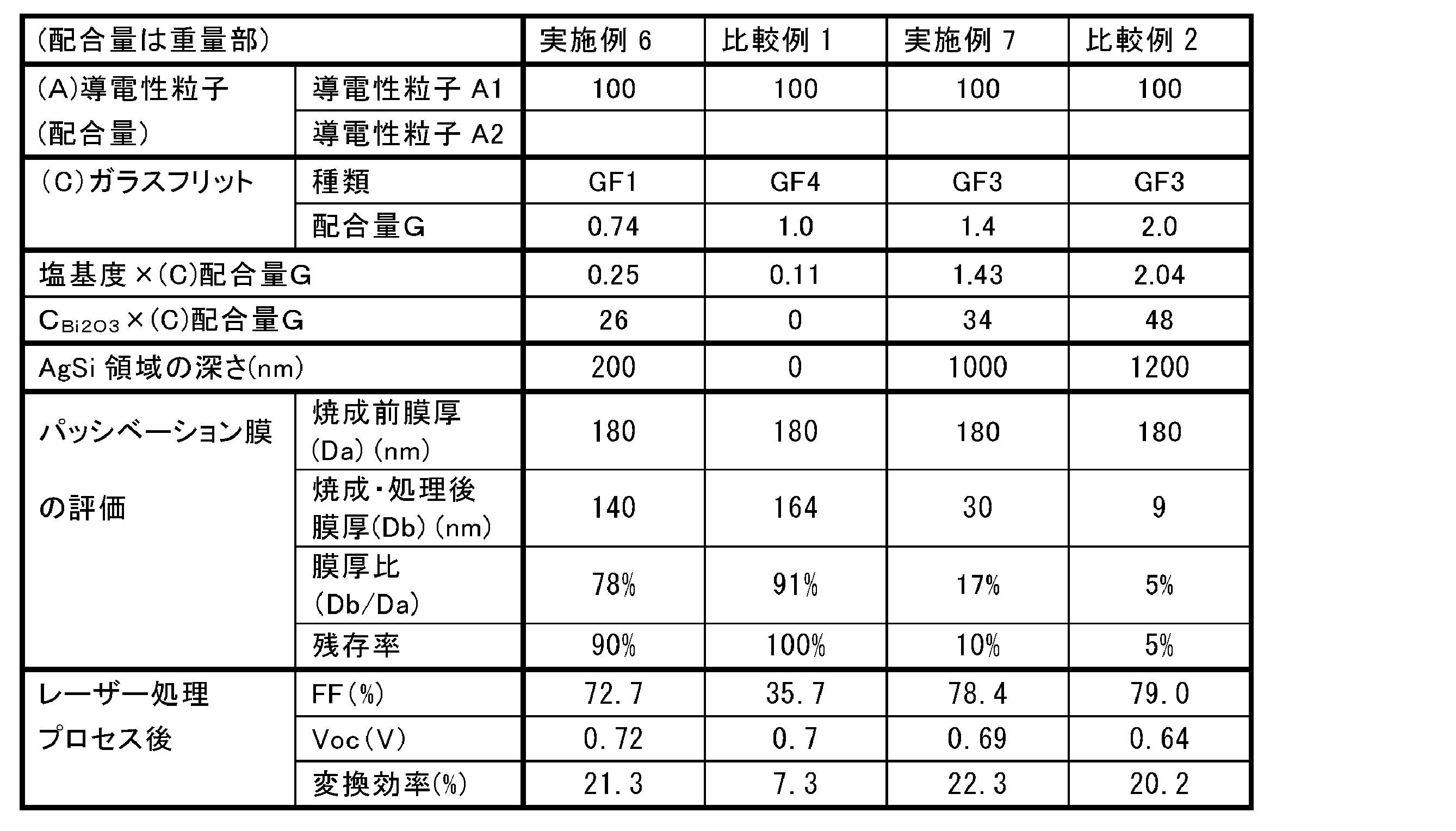

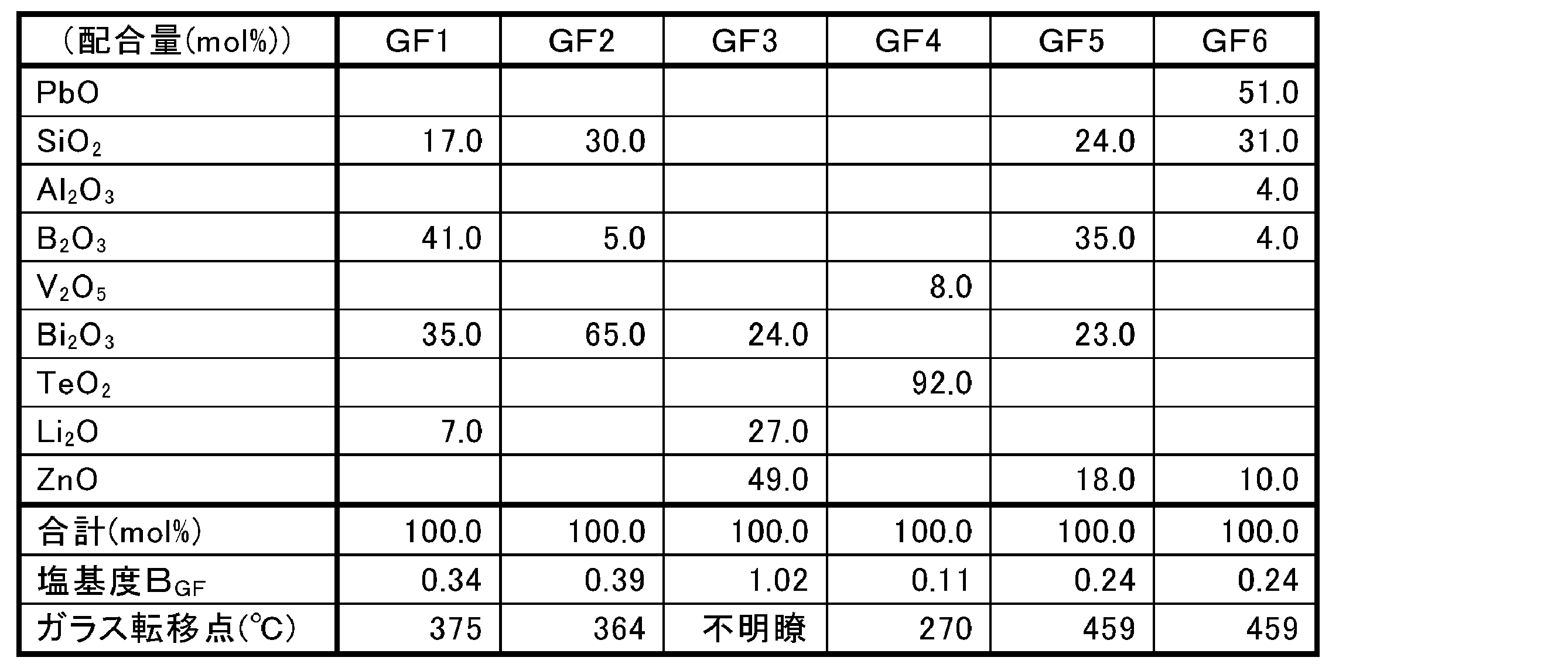
2 パッシベーション膜
4 不純物拡散層
6 基板本体
14 裏面パッシベーション膜
15 裏面電極
15a 裏面TAB電極(裏面バスバー電極)
15b 裏面全面電極
15c 裏面フィンガー電極
16 第2の不純物拡散層
20 光入射側表面電極(表面電極)
20a 光入射側バスバー電極
20b 光入射側フィンガー電極
30 AgSi領域
Claims (9)
- 結晶系シリコンを含む基板であって、少なくとも一方の表面に不純物拡散層を含む前記基板と、
前記基板の前記不純物拡散層の少なくとも一部の上に配置されたパッシベーション膜と、
銀(Ag)を含む電極であって、前記パッシベーション膜の少なくとも一部の上に配置された前記電極と
を含む太陽電池であって、
前記太陽電池が、前記電極と、前記基板との間の少なくとも一部に配置された、少なくとも1つのAgSi領域を更に含み、
前記AgSi領域が、深さが100nm以上のAgSi領域を少なくとも1つ含み、
前記太陽電池の前記AgSi領域を含む5.7μm×3.9μmの断面の走査型電子顕微鏡写真において、前記パッシベーション膜が残存している長さの割合である前記パッシベーション膜の残存率が、10~90%である、太陽電池。 - 前記パッシベーション膜の成膜直後の膜厚Daと、前記太陽電池の表面に前記電極が形成されて完成した前記太陽電池の前記AgSi領域を含む5.7μm×3.9μmの断面の走査型電子顕微鏡写真における前記パッシベーション膜の膜厚Dbとの比Db/Daが、15%~85%である、請求項1に記載の太陽電池。
- 前記電極が、前記電極に含まれる前記銀(Ag)の100重量部に対して0.1~5.0重量部のガラスフリットを更に含む、請求項1又は2に記載の太陽電池。
- 前記ガラスフリットのガラス転移点が250~600℃である、請求項3に記載の太陽電池。
- 前記ガラスフリットが、SiO2、B2O3、V2O5、Bi2O3、TeO2、Li2O及びZnOから選択される少なくとも1つを含む、請求項3又は4に記載の太陽電池。
- 前記ガラスフリットが、PbOを実質的に含まない、請求項3~5のいずれか1項に記載の太陽電池。
- 前記電極が鉛(Pb)を実質的に含まない、請求項1~6のいずれか1項に記載の太陽電池。
- 前記電極がアルミニウム粒子を実質的に含まない、請求項1~7のいずれか1項に記載の太陽電池。
- 前記基板が、第1の導電型の前記結晶系シリコン基板であり、
前記不純物拡散層が、第2の導電型の不純物拡散層であり、
前記電極が、光入射側表面に配置された光入射側表面電極であり、
前記太陽電池が、前記結晶系シリコン基板の前記光入射側表面とは反対側の表面に対して電気的に接続するように配置された裏面電極を更に含み、
前記光入射側表面電極が、前記第2の導電型の前記不純物拡散層と、前記第1の導電型の前記結晶系シリコン基板との間で順方向とは逆向きの電流が流れるように、前記裏面電極と、前記光入射側表面電極との間に電圧を印加しながら、点光源からの光を前記太陽電池の前記光入射側表面に照射する処理をした前記光入射側表面電極である、請求項1~8のいずれか1項に記載の太陽電池。
Priority Applications (4)
| Application Number | Priority Date | Filing Date | Title |
|---|---|---|---|
| KR1020257018223A KR20250108642A (ko) | 2022-11-07 | 2023-08-09 | 태양 전지 |
| EP23888302.9A EP4618162A4 (en) | 2022-11-07 | 2023-08-09 | SOLAR CELL |
| CN202380077093.5A CN120092512A (zh) | 2022-11-07 | 2023-08-09 | 太阳能电池 |
| JP2024557029A JPWO2024100947A1 (ja) | 2022-11-07 | 2023-08-09 |
Applications Claiming Priority (6)
| Application Number | Priority Date | Filing Date | Title |
|---|---|---|---|
| JP2022-178203 | 2022-11-07 | ||
| JP2022178203 | 2022-11-07 | ||
| PCT/JP2023/012085 WO2023190282A1 (ja) | 2022-03-28 | 2023-03-27 | 導電性ペースト、太陽電池及び太陽電池の製造方法 |
| JPPCT/JP2023/012085 | 2023-03-27 | ||
| JP2023-096794 | 2023-06-13 | ||
| JP2023096794 | 2023-06-13 |
Publications (1)
| Publication Number | Publication Date |
|---|---|
| WO2024100947A1 true WO2024100947A1 (ja) | 2024-05-16 |
Family
ID=91032119
Family Applications (1)
| Application Number | Title | Priority Date | Filing Date |
|---|---|---|---|
| PCT/JP2023/029078 Ceased WO2024100947A1 (ja) | 2022-11-07 | 2023-08-09 | 太陽電池 |
Country Status (6)
| Country | Link |
|---|---|
| EP (1) | EP4618162A4 (ja) |
| JP (1) | JPWO2024100947A1 (ja) |
| KR (1) | KR20250108642A (ja) |
| CN (1) | CN120092512A (ja) |
| TW (1) | TW202420608A (ja) |
| WO (1) | WO2024100947A1 (ja) |
Citations (7)
| Publication number | Priority date | Publication date | Assignee | Title |
|---|---|---|---|---|
| JP2009231826A (ja) | 2008-02-26 | 2009-10-08 | Mitsubishi Materials Corp | 導電性組成物及びそれを用いた太陽電池セルとその製造方法並びに該太陽電池セルを用いて形成された太陽電池モジュール |
| JP2011086754A (ja) | 2009-10-15 | 2011-04-28 | Namics Corp | 太陽電池及びその製造方法 |
| US20110278507A1 (en) * | 2010-05-11 | 2011-11-17 | E. I. Du Pont De Nemours And Company | Thick film silver pastes containing iodonium and/or sulfonium salts and their use in photovoltaic cells |
| JP2014078594A (ja) * | 2012-10-10 | 2014-05-01 | Noritake Co Ltd | ペースト組成物と太陽電池 |
| JP2014150015A (ja) * | 2013-02-04 | 2014-08-21 | Namics Corp | 太陽電池の電極形成用導電性ペースト |
| JP2015050277A (ja) * | 2013-08-30 | 2015-03-16 | シャープ株式会社 | 太陽電池およびその製造方法 |
| JP2021513218A (ja) | 2018-02-07 | 2021-05-20 | シーイー セル エンジニアリング ゲーエムベーハー | シリコンソーラセルのコンタクトグリッドとエミッタレイヤ間のオーミックコンタクト挙動を改善する方法 |
Family Cites Families (4)
| Publication number | Priority date | Publication date | Assignee | Title |
|---|---|---|---|---|
| US20100224243A1 (en) * | 2009-03-05 | 2010-09-09 | Applied Materials, Inc. | Adhesion between azo and ag for the back contact in tandem junction cell by metal alloy |
| CN102157220B (zh) * | 2011-02-28 | 2013-09-18 | 张振中 | 晶体硅太阳能电池正面栅线电极专用Ag浆 |
| CN105408267B (zh) * | 2013-07-25 | 2020-01-14 | 纳美仕有限公司 | 结晶系硅太阳能电池及其制造方法 |
| CN114242803B (zh) * | 2022-02-25 | 2022-08-12 | 浙江晶科能源有限公司 | 太阳能电池及其制备方法、光伏组件 |
-
2023
- 2023-08-09 WO PCT/JP2023/029078 patent/WO2024100947A1/ja not_active Ceased
- 2023-08-09 JP JP2024557029A patent/JPWO2024100947A1/ja active Pending
- 2023-08-09 CN CN202380077093.5A patent/CN120092512A/zh active Pending
- 2023-08-09 TW TW112129981A patent/TW202420608A/zh unknown
- 2023-08-09 EP EP23888302.9A patent/EP4618162A4/en active Pending
- 2023-08-09 KR KR1020257018223A patent/KR20250108642A/ko active Pending
Patent Citations (7)
| Publication number | Priority date | Publication date | Assignee | Title |
|---|---|---|---|---|
| JP2009231826A (ja) | 2008-02-26 | 2009-10-08 | Mitsubishi Materials Corp | 導電性組成物及びそれを用いた太陽電池セルとその製造方法並びに該太陽電池セルを用いて形成された太陽電池モジュール |
| JP2011086754A (ja) | 2009-10-15 | 2011-04-28 | Namics Corp | 太陽電池及びその製造方法 |
| US20110278507A1 (en) * | 2010-05-11 | 2011-11-17 | E. I. Du Pont De Nemours And Company | Thick film silver pastes containing iodonium and/or sulfonium salts and their use in photovoltaic cells |
| JP2014078594A (ja) * | 2012-10-10 | 2014-05-01 | Noritake Co Ltd | ペースト組成物と太陽電池 |
| JP2014150015A (ja) * | 2013-02-04 | 2014-08-21 | Namics Corp | 太陽電池の電極形成用導電性ペースト |
| JP2015050277A (ja) * | 2013-08-30 | 2015-03-16 | シャープ株式会社 | 太陽電池およびその製造方法 |
| JP2021513218A (ja) | 2018-02-07 | 2021-05-20 | シーイー セル エンジニアリング ゲーエムベーハー | シリコンソーラセルのコンタクトグリッドとエミッタレイヤ間のオーミックコンタクト挙動を改善する方法 |
Non-Patent Citations (2)
| Title |
|---|
| K. MORINAGAH. YOSHIDAH. TAKEBE, J. AMCERM. SOC., vol. 77, 1994, pages 3113 |
| See also references of EP4618162A1 |
Also Published As
| Publication number | Publication date |
|---|---|
| KR20250108642A (ko) | 2025-07-15 |
| EP4618162A1 (en) | 2025-09-17 |
| JPWO2024100947A1 (ja) | 2024-05-16 |
| TW202420608A (zh) | 2024-05-16 |
| EP4618162A4 (en) | 2026-04-15 |
| CN120092512A (zh) | 2025-06-03 |
Similar Documents
| Publication | Publication Date | Title |
|---|---|---|
| US7435361B2 (en) | Conductive compositions and processes for use in the manufacture of semiconductor devices | |
| CN1862839B (zh) | 半导体器件的制造方法及其中用到的导电组合物 | |
| JP5349738B2 (ja) | 半導体デバイスの製造方法、およびそこで使用される導電性組成物 | |
| JP6714275B2 (ja) | 導電性ペースト及び太陽電池 | |
| WO2009052271A1 (en) | Lead-free conductive compositions and processes for use in the manufacture of semiconductor devices: mg-containing additive | |
| EP2191480A1 (en) | Conductive compositions and processes for use in the manufacture of semiconductor devices: flux materials | |
| EP4503141A1 (en) | Electrically conductive paste, solar cell, and method for manufacturing solar cell | |
| CN108701504A (zh) | 导电性糊剂和太阳能电池 | |
| JP6137852B2 (ja) | 太陽電池の電極形成用導電性ペースト | |
| JP6580383B2 (ja) | 導電性ペースト、太陽電池及び太陽電池の製造方法 | |
| JP2009194121A (ja) | 結晶系シリコン太陽電池電極形成用導電性ペースト | |
| JP6688500B2 (ja) | 導電性ペースト及び太陽電池 | |
| WO2024101223A1 (ja) | 導電性ペースト、太陽電池及び太陽電池の製造方法 | |
| WO2024100947A1 (ja) | 太陽電池 | |
| WO2024257439A1 (ja) | 導電性ペースト、導電性ペーストの使用、太陽電池及び太陽電池の製造方法 |
Legal Events
| Date | Code | Title | Description |
|---|---|---|---|
| 121 | Ep: the epo has been informed by wipo that ep was designated in this application |
Ref document number: 23888302 Country of ref document: EP Kind code of ref document: A1 |
|
| WWE | Wipo information: entry into national phase |
Ref document number: 2024557029 Country of ref document: JP |
|
| WWE | Wipo information: entry into national phase |
Ref document number: 202380077093.5 Country of ref document: CN |
|
| WWE | Wipo information: entry into national phase |
Ref document number: 1020257018223 Country of ref document: KR |
|
| WWP | Wipo information: published in national office |
Ref document number: 202380077093.5 Country of ref document: CN |
|
| WWE | Wipo information: entry into national phase |
Ref document number: 2023888302 Country of ref document: EP |
|
| NENP | Non-entry into the national phase |
Ref country code: DE |
|
| ENP | Entry into the national phase |
Ref document number: 2023888302 Country of ref document: EP Effective date: 20250610 |
|
| WWP | Wipo information: published in national office |
Ref document number: 1020257018223 Country of ref document: KR |
|
| WWP | Wipo information: published in national office |
Ref document number: 2023888302 Country of ref document: EP |