WO2024116660A1 - 位置検出装置 - Google Patents
位置検出装置 Download PDFInfo
- Publication number
- WO2024116660A1 WO2024116660A1 PCT/JP2023/038359 JP2023038359W WO2024116660A1 WO 2024116660 A1 WO2024116660 A1 WO 2024116660A1 JP 2023038359 W JP2023038359 W JP 2023038359W WO 2024116660 A1 WO2024116660 A1 WO 2024116660A1
- Authority
- WO
- WIPO (PCT)
- Prior art keywords
- spiral portion
- spiral
- line
- receiving coil
- coil
- Prior art date
- Legal status (The legal status is an assumption and is not a legal conclusion. Google has not performed a legal analysis and makes no representation as to the accuracy of the status listed.)
- Ceased
Links
Images






Classifications
-
- G—PHYSICS
- G01—MEASURING; TESTING
- G01D—MEASURING NOT SPECIALLY ADAPTED FOR A SPECIFIC VARIABLE; ARRANGEMENTS FOR MEASURING TWO OR MORE VARIABLES NOT COVERED IN A SINGLE OTHER SUBCLASS; TARIFF METERING APPARATUS; MEASURING OR TESTING NOT OTHERWISE PROVIDED FOR
- G01D5/00—Mechanical means for transferring the output of a sensing member; Means for converting the output of a sensing member to another variable where the form or nature of the sensing member does not constrain the means for converting; Transducers not specially adapted for a specific variable
- G01D5/12—Mechanical means for transferring the output of a sensing member; Means for converting the output of a sensing member to another variable where the form or nature of the sensing member does not constrain the means for converting; Transducers not specially adapted for a specific variable using electric or magnetic means
- G01D5/14—Mechanical means for transferring the output of a sensing member; Means for converting the output of a sensing member to another variable where the form or nature of the sensing member does not constrain the means for converting; Transducers not specially adapted for a specific variable using electric or magnetic means influencing the magnitude of a current or voltage
- G01D5/20—Mechanical means for transferring the output of a sensing member; Means for converting the output of a sensing member to another variable where the form or nature of the sensing member does not constrain the means for converting; Transducers not specially adapted for a specific variable using electric or magnetic means influencing the magnitude of a current or voltage by varying inductance, e.g. by a movable armature
- G01D5/204—Mechanical means for transferring the output of a sensing member; Means for converting the output of a sensing member to another variable where the form or nature of the sensing member does not constrain the means for converting; Transducers not specially adapted for a specific variable using electric or magnetic means influencing the magnitude of a current or voltage by varying inductance, e.g. by a movable armature by influencing the mutual induction between two or more coils
- G01D5/2053—Mechanical means for transferring the output of a sensing member; Means for converting the output of a sensing member to another variable where the form or nature of the sensing member does not constrain the means for converting; Transducers not specially adapted for a specific variable using electric or magnetic means influencing the magnitude of a current or voltage by varying inductance, e.g. by a movable armature by influencing the mutual induction between two or more coils by a movable non-ferromagnetic conductive element
-
- G—PHYSICS
- G01—MEASURING; TESTING
- G01D—MEASURING NOT SPECIALLY ADAPTED FOR A SPECIFIC VARIABLE; ARRANGEMENTS FOR MEASURING TWO OR MORE VARIABLES NOT COVERED IN A SINGLE OTHER SUBCLASS; TARIFF METERING APPARATUS; MEASURING OR TESTING NOT OTHERWISE PROVIDED FOR
- G01D5/00—Mechanical means for transferring the output of a sensing member; Means for converting the output of a sensing member to another variable where the form or nature of the sensing member does not constrain the means for converting; Transducers not specially adapted for a specific variable
- G01D5/12—Mechanical means for transferring the output of a sensing member; Means for converting the output of a sensing member to another variable where the form or nature of the sensing member does not constrain the means for converting; Transducers not specially adapted for a specific variable using electric or magnetic means
- G01D5/14—Mechanical means for transferring the output of a sensing member; Means for converting the output of a sensing member to another variable where the form or nature of the sensing member does not constrain the means for converting; Transducers not specially adapted for a specific variable using electric or magnetic means influencing the magnitude of a current or voltage
- G01D5/20—Mechanical means for transferring the output of a sensing member; Means for converting the output of a sensing member to another variable where the form or nature of the sensing member does not constrain the means for converting; Transducers not specially adapted for a specific variable using electric or magnetic means influencing the magnitude of a current or voltage by varying inductance, e.g. by a movable armature
-
- G—PHYSICS
- G01—MEASURING; TESTING
- G01D—MEASURING NOT SPECIALLY ADAPTED FOR A SPECIFIC VARIABLE; ARRANGEMENTS FOR MEASURING TWO OR MORE VARIABLES NOT COVERED IN A SINGLE OTHER SUBCLASS; TARIFF METERING APPARATUS; MEASURING OR TESTING NOT OTHERWISE PROVIDED FOR
- G01D5/00—Mechanical means for transferring the output of a sensing member; Means for converting the output of a sensing member to another variable where the form or nature of the sensing member does not constrain the means for converting; Transducers not specially adapted for a specific variable
- G01D5/12—Mechanical means for transferring the output of a sensing member; Means for converting the output of a sensing member to another variable where the form or nature of the sensing member does not constrain the means for converting; Transducers not specially adapted for a specific variable using electric or magnetic means
- G01D5/14—Mechanical means for transferring the output of a sensing member; Means for converting the output of a sensing member to another variable where the form or nature of the sensing member does not constrain the means for converting; Transducers not specially adapted for a specific variable using electric or magnetic means influencing the magnitude of a current or voltage
- G01D5/20—Mechanical means for transferring the output of a sensing member; Means for converting the output of a sensing member to another variable where the form or nature of the sensing member does not constrain the means for converting; Transducers not specially adapted for a specific variable using electric or magnetic means influencing the magnitude of a current or voltage by varying inductance, e.g. by a movable armature
- G01D5/204—Mechanical means for transferring the output of a sensing member; Means for converting the output of a sensing member to another variable where the form or nature of the sensing member does not constrain the means for converting; Transducers not specially adapted for a specific variable using electric or magnetic means influencing the magnitude of a current or voltage by varying inductance, e.g. by a movable armature by influencing the mutual induction between two or more coils
- G01D5/2053—Mechanical means for transferring the output of a sensing member; Means for converting the output of a sensing member to another variable where the form or nature of the sensing member does not constrain the means for converting; Transducers not specially adapted for a specific variable using electric or magnetic means influencing the magnitude of a current or voltage by varying inductance, e.g. by a movable armature by influencing the mutual induction between two or more coils by a movable non-ferromagnetic conductive element
- G01D5/206—Mechanical means for transferring the output of a sensing member; Means for converting the output of a sensing member to another variable where the form or nature of the sensing member does not constrain the means for converting; Transducers not specially adapted for a specific variable using electric or magnetic means influencing the magnitude of a current or voltage by varying inductance, e.g. by a movable armature by influencing the mutual induction between two or more coils by a movable non-ferromagnetic conductive element constituting a short-circuiting element
-
- G—PHYSICS
- G01—MEASURING; TESTING
- G01D—MEASURING NOT SPECIALLY ADAPTED FOR A SPECIFIC VARIABLE; ARRANGEMENTS FOR MEASURING TWO OR MORE VARIABLES NOT COVERED IN A SINGLE OTHER SUBCLASS; TARIFF METERING APPARATUS; MEASURING OR TESTING NOT OTHERWISE PROVIDED FOR
- G01D5/00—Mechanical means for transferring the output of a sensing member; Means for converting the output of a sensing member to another variable where the form or nature of the sensing member does not constrain the means for converting; Transducers not specially adapted for a specific variable
- G01D5/12—Mechanical means for transferring the output of a sensing member; Means for converting the output of a sensing member to another variable where the form or nature of the sensing member does not constrain the means for converting; Transducers not specially adapted for a specific variable using electric or magnetic means
- G01D5/14—Mechanical means for transferring the output of a sensing member; Means for converting the output of a sensing member to another variable where the form or nature of the sensing member does not constrain the means for converting; Transducers not specially adapted for a specific variable using electric or magnetic means influencing the magnitude of a current or voltage
- G01D5/20—Mechanical means for transferring the output of a sensing member; Means for converting the output of a sensing member to another variable where the form or nature of the sensing member does not constrain the means for converting; Transducers not specially adapted for a specific variable using electric or magnetic means influencing the magnitude of a current or voltage by varying inductance, e.g. by a movable armature
- G01D5/204—Mechanical means for transferring the output of a sensing member; Means for converting the output of a sensing member to another variable where the form or nature of the sensing member does not constrain the means for converting; Transducers not specially adapted for a specific variable using electric or magnetic means influencing the magnitude of a current or voltage by varying inductance, e.g. by a movable armature by influencing the mutual induction between two or more coils
- G01D5/2066—Mechanical means for transferring the output of a sensing member; Means for converting the output of a sensing member to another variable where the form or nature of the sensing member does not constrain the means for converting; Transducers not specially adapted for a specific variable using electric or magnetic means influencing the magnitude of a current or voltage by varying inductance, e.g. by a movable armature by influencing the mutual induction between two or more coils by movement of a single coil with respect to a single other coil
Definitions
- This disclosure relates to a position detection device.
- Position detection devices have been proposed in the past for detecting the position of an object to be detected.
- the position detection device described in Patent Document 1 includes a transmitting coil and a receiving coil mounted on a substrate, and a target arranged opposite the substrate.
- the receiving coil has multiple spiral sections in which the wiring is formed into a spiral shape, and connection wires that electrically connect the multiple spiral sections together.
- This position detection device applies an alternating current to the transmitting coil, and detects the position of the target based on a characteristic value (e.g., output voltage) of the receiving coil that changes according to the amount of displacement of the target.
- a characteristic value e.g., output voltage
- a position detection device for detecting the position of a displaceable detectable object includes a substrate arranged opposite the detectable object, a transmitting coil extending in the surface direction of the substrate, a plurality of spiral portions in which wiring is formed in a spiral shape and aligned in the displacement direction of the detectable object, and which are inductively coupled by electromagnetic induction caused by passing current through the transmitting coil, connecting wires that electrically connect the plurality of spiral portions together, and a receiving coil having parallel wires that are electrically connected to the spiral portions and the connecting wires and run parallel to the connecting wires.
- this position detection device can improve detection accuracy by preventing the characteristic value of the receiving coil from going outside the adjustment range of the signal processing unit.
- At least a portion of the magnetic field generated by the current flowing through the connection line and at least a portion of the magnetic field generated by the current flowing through the parallel line cancel each other out may mean that the entire magnetic field is canceled out, or that only a portion of the magnetic field is canceled out.
- this position detection device has multiple spiral sections, it is possible to increase the occupancy rate of the wiring of the receiving coil per unit area of the board (hereinafter referred to as the "space factor"). As a result, this position detection device is able to increase the amplitude of the output voltage of the receiving coil, improving detection accuracy.
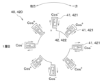
- FIG. 1 is a plan view showing a position detection device according to a first embodiment.
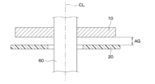
- 2 is a cross-sectional view taken along line II-II of FIG. 1.
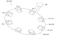
- FIG. 2 is a perspective view showing a first receiving coil according to the first embodiment.
- FIG. 2 is a perspective view showing a second receiving coil according to the first embodiment.
- 4 is a diagram showing a portion of the first receiving coil mounted on a first layer of a multilayer substrate.
- FIG. 4 is a diagram showing a portion of the first receiving coil mounted on a second layer of a multilayer substrate.
- FIG. 13 is a diagram showing a portion of the first receiving coil mounted on a third layer of a multilayer substrate.
- FIG. 13 is a diagram showing a portion of the second receiving coil mounted on a first layer of a multilayer substrate.
- FIG. 13 is a diagram showing a portion of the second receiving coil mounted on a second layer of a multilayer substrate.
- FIG. 13 is a diagram showing a portion of the second receiving coil mounted on a third layer of a multilayer substrate.
- FIG. 11 is a graph showing the output voltage of a first receiving coil and the output voltage of a second receiving coil.
- 1 is a block diagram of a position detection device according to a first embodiment.
- FIG. 11 is a graph comparing the amplitude of the output voltage of the first receiving coil provided in the position detection device of the first embodiment with the amplitude of the output voltage of the first receiving coil provided in the position detection device of the first comparative example (i.e., one that does not have a spiral portion). 13 is a graph comparing the output voltage of the first receiving coil provided in the position detection device of the first embodiment with the output voltage of the first receiving coil provided in the position detection device of the second comparative example (i.e., one that does not have a parallel line).
- FIG. 11 is a plan view showing a position detection device according to a second embodiment.
- FIG. 11 is a perspective view showing a first receiving coil according to a second embodiment.
- FIG. 11 is a perspective view showing a second receiving coil according to the second embodiment.
- FIG. 2 is a plan view showing a position detection device of a first comparative example.
- FIG. 11 is a perspective view showing a first receiving coil of a second comparative example.
- FIG. 11 is a perspective view showing a second receiving coil of a second comparative example.
- the position detection device is an inductive sensor that includes a substrate 20, a transmitting coil 30, a receiving coil 40, and a signal processing unit 50, and detects the position of a target 10 as a detected object.
- the substrate 20 a transmitting coil 30, a receiving coil 40, and a signal processing unit 50, and detects the position of a target 10 as a detected object.
- wiring arranged on multiple layers of the substrate 20 is shown overlapping.
- Figures 3 to 6C in this embodiment, an example will be described in which wiring constituting the receiving coil 40 and the like is provided on three layers of the substrate 20.
- the target 10 is made of a conductor such as metal and is fixed to the rotating shaft 60.
- the target 10 undergoes rotational displacement together with the rotating shaft 60, centered on the axis CL of the rotating shaft 60.
- the target 10 may undergo rotational displacement of 360 degrees or more, or may undergo rotational displacement within a range of 360 degrees or less.
- the direction in which the axis CL of the rotating shaft 60 extends is referred to as the "axial direction”
- the radial direction of an imaginary circle perpendicular to the axis CL of the rotating shaft 60 is referred to as the "radial direction”
- the circumferential direction of the imaginary circle is referred to as the "circumferential direction”.
- the target 10 is formed in a substantially circular ring shape.
- the target 10 has one or more (e.g., four) teeth 11 in the circumferential direction and one or more (e.g., four) openings 12 formed between the teeth 11.
- the teeth 11 and openings 12 are aligned in the displacement direction of the target 10 (i.e., the circumferential direction).
- the shape and size of the teeth 11 and openings 12 of the target 10 are not limited to those shown in FIG. 1, and are set appropriately depending on, for example, the magnitude of the output voltage of the receiving coil 40 required for signal processing by the signal processing unit 50.
- the substrate 20 is, for example, a multi-layer substrate, and is disposed opposite the target 10.
- a predetermined gap AG is provided between the substrate 20 and the target 10.
- the substrate 20 is fixed to a fixed body (not shown) (for example, a vehicle body or a member fixed to the vehicle body). Therefore, the rotation shaft 60 and the target 10 rotate relative to the substrate 20.
- the transmitting coil 30 is provided on any layer of the substrate 20 and extends in the surface direction of the substrate 20.
- the transmitting coil 30 is wound multiple times so as to surround the radial outside of the receiving coil 40.
- One end and the other end of the wiring of the transmitting coil 30 are each connected to the signal processing unit 50.
- the receiving coil 40 has multiple spiral parts 41, connection lines 42, parallel lines 43, etc.
- the multiple spiral parts 41 are parts where the wiring is formed in a spiral shape.
- the multiple spiral parts 41 are arranged at positions where they are inductively coupled by electromagnetic induction caused by current passing through the transmitting coil 30.
- the multiple spiral parts 41 are lined up in the displacement direction of the target 10.
- the direction in which the multiple spiral parts 41 are lined up is substantially the same as the direction in which the transmitting coil 30 extends. Therefore, the multiple spiral parts 41 are lined up in the direction in which the transmitting coil 30 extends.
- the multiple spiral parts 41 are arranged radially inside the transmitting coil 30, which is wound in a ring shape. It is preferable that the wiring that constitutes the multiple spiral parts 41 is arranged with the maximum space factor while ensuring the clearance required for insulation.
- connection wires 42 are parts that electrically connect the multiple spiral portions 41 together. Therefore, the connection wires 42 are provided at multiple locations between the multiple spiral portions 41.
- the parallel wire 43 is electrically connected to the spiral portion 41 and the connection wire 42, and runs parallel to the connection wire 42.
- the parallel wire 43 runs parallel to at least some or all of the connection wires 42 at multiple locations.
- the receiving coil 40 has a first receiving coil 410 and a second receiving coil 420.
- the first receiving coil 410 has a plurality of first spiral portions 411, a first connecting line 412, a first parallel line 413, and the like. Note that circles in Figures 5A to 5C indicate vias. In other words, the plurality of first spiral portions 411, the first connecting line 412, the first parallel line 413, and the like that constitute the first receiving coil 410 are electrically connected in a single stroke through vias.
- one of the first spiral parts 411 arranged on either side of a given second spiral part 421 may be referred to as a Sin+ coil, and the other first spiral part 411 may be referred to as a Sin- coil, as shown in FIG. 1 etc.
- each first spiral portion 411 indicates the direction in which current flows through the wiring of each first spiral portion 411 at a given instantaneous value of the AC current applied to the transmission coil 30.
- current flows counterclockwise in one first spiral portion 411 (e.g., Sin+ coil) and current flows clockwise in the other first spiral portion 411 (e.g., Sin- coil).
- the first receiving coil 410 is a receiving coil 40 that outputs a sine wave signal in response to the displacement of the target 10.
- the first receiving coil 410 outputs a voltage value corresponding to the magnitude of the induced current generated from the Sin+ coil and the Sin- coil located at a position corresponding to the opening 12 of the target 10.
- the distance between the center of the Sin+ coil and the center of the Sin- coil is set so that the phase of the waveform of the output voltage corresponding to the amount of displacement of the target 10 differs by 180 degrees in electrical angle.
- the first connection wires 412 electrically connect the multiple first spiral portions 411 to each other.
- each of the first connection wires 412 connects the radially outer portions of the multiple first spiral portions 411 to each other.
- the first parallel line 413 is electrically connected to the multiple first spiral portions 411 and the first connection line 412 and runs parallel to the first connection line 412.
- the first parallel line 413 is provided in a different layer from the first connection line 412, at a position where it overlaps with the thickness direction of the substrate 20. Therefore, in this embodiment, the first parallel line 413 is provided at a position radially outside the multiple first spiral portions 411.
- the first connection line 412 and the first parallel line 413 are electrically connected via a first fold 414.
- the first fold 414 is formed by a via that electrically connects the first connection line 412 and the first parallel line 413 provided on two different layers of the substrate 20.
- the first connection line 412 and the first parallel line 413 are arranged so as to fold back via the via as the first fold 414 on the two different layers of the substrate 20. Therefore, the first connection line 412 and the first parallel line 413 are arranged such that, at a given instantaneous value of the AC current applied to the transmission coil 30, the direction of the current flowing through a given portion of the first connection line 412 is opposite to the direction of the current flowing through a given portion of the first parallel line 413 adjacent to that portion.
- the first connection line 412 and the first parallel line 413 are provided in two different layers of the substrate 20 at positions where they overlap in the thickness direction of the substrate 20. Therefore, the first connection line 412 and the first parallel line 413 are arranged adjacent to each other. Specifically, the adjacent arrangement means that they are arranged at a distance where at least a part of the magnetic field generated by the current flowing in the first connection line 412 due to the AC current applied to the transmission coil 30 and at least a part of the magnetic field generated by the current flowing in the first parallel line 413 cancel each other out.
- the second receiving coil 420 has a plurality of second spiral portions 421, a second connecting line 422, a second parallel line 423, and the like.
- the circles in Figures 6A to 6C also represent vias.
- the plurality of second spiral portions 421, the second connecting line 422, the second parallel line 423, and the like that constitute the second receiving coil 420 are electrically connected in a single stroke through the vias.
- one of the second spiral parts 421 arranged on either side of a given first spiral part 411 may be referred to as a Cos+ coil, and the other second spiral part 421 may be referred to as a Cos- coil.
- each second spiral portion 421 the arrows drawn on the outside of each second spiral portion 421 indicate the direction in which current flows through the wiring of each second spiral portion 421 at different instantaneous values of the AC current applied to the transmission coil 30.
- current flows counterclockwise in one second spiral portion 421 e.g., Cos+ coil
- current flows clockwise in the other second spiral portion 421 e.g., Cos- coil.
- the second receiving coil 420 is a receiving coil 40 that outputs a sine-wave voltage signal that is out of phase with the waveform of the voltage signal of the first receiving coil 410 in response to the displacement of the target 10.
- the waveform of the output voltage of the first receiving coil 410 and the waveform of the output voltage of the second receiving coil 420 differ by 90 degrees in electrical angle. Therefore, the waveform of the output voltage of the second receiving coil 420 can also be said to be cosine-wave shaped.
- the second receiving coil 420 outputs a voltage value that corresponds to the magnitude of the induced current generated from the Cos+ coil and the Cos- coil located at a position corresponding to the opening 12 of the target 10.
- the distance between the center of the Cos+ coil and the center of the Cos- coil is set so that the phases of the waveforms of the output voltages corresponding to the displacement of the target 10 differ by 180 degrees in electrical angle.
- the distance between the center of the Sin+ coil and the center of the Cos+ coil is set so that the phases of the waveforms of the output voltages corresponding to the displacement of the target 10 differ by 90 degrees in electrical angle.
- the distance between the center of the Sin- coil and the center of the Cos- coil is set so that the phases of the waveforms of the output voltages corresponding to the displacement of the target 10 differ by 90 degrees in electrical angle.
- the second connection wires 422 electrically connect the multiple second spiral portions 421 to each other.
- each of the second connection wires 422 connects the radially inner portions of the multiple second spiral portions 421 to each other.
- the second parallel line 423 is electrically connected to the multiple second spiral portions 421 and the second connection line 422 and runs parallel to the second connection line 422.
- the second parallel line 423 is provided in a different layer from the second connection line 422 and at a position where it overlaps in the thickness direction of the substrate 20. Therefore, in this embodiment, the second parallel line 423 is provided at a position radially inward of the multiple second spiral portions 421.
- the second connection line 422 and the second parallel line 423 are electrically connected via a second fold-back portion 424.
- the second fold-back portion 424 is formed by a via that electrically connects the second connection line 422 and the second parallel line 423, which are provided on two different layers of the substrate 20.
- the second connection line 422 and the second parallel line 423 are arranged so as to fold back via the via as the second fold-back portion 424 on the two different layers of the substrate 20.
- the second connection line 422 and the second parallel line 423 are arranged such that, at a given instantaneous value of the AC current applied to the transmission coil 30, the direction of the current flowing through a given portion of the second connection line 422 is opposite to the direction of the current flowing through a given portion of the second parallel line 423 adjacent to that portion.
- the second connection line 422 and the second parallel line 423 are provided in two different layers of the substrate 20 at positions where they overlap in the thickness direction of the substrate 20. Therefore, the second connection line 422 and the second parallel line 423 are arranged adjacent to each other. Specifically, the adjacent arrangement means that they are arranged at a distance where at least a part of the magnetic field generated by the current flowing in the second connection line 422 due to the AC current applied to the transmission coil 30 and at least a part of the magnetic field generated by the current flowing in the second parallel line 423 cancel each other out.
- the board 20 is provided with an electronic control circuit 21 that includes a microcomputer with a processor and memory.
- the electronic control circuit 21 executes various control operations by having the processor read and execute a program from the memory.
- the memory stores various data to be used when executing the program.
- the electronic control circuit 21 is equipped with a signal processing unit 50 that is connected to the transmitting coil 30, the first receiving coil 410, and the second receiving coil 420 and performs predetermined processing.
- the signal processing unit 50 has, for example, an oscillator 51, a demodulator 52, an AD converter 53, an offset and gain correction unit 54, an angle calculator 55, an output unit 56, etc., and is configured with an integrated circuit (IC). Note that, although the following describes a representative example of conversion to a digital signal for processing, when processing an analog signal, the signal processing unit 50 does not need to include the AD converter 53, etc.
- the oscillator 51 is electrically connected to the transmitting coil 30 and applies an alternating current of a predetermined frequency to the transmitting coil 30. At that time, an induced current flows in the first receiving coil 410 and the second receiving coil 420 due to the magnetic field generated by the transmitting coil 30.
- the demodulation unit 52 is connected to each of the first receiving coil 410 and the second receiving coil 420.
- the demodulation unit 52 generates a first demodulated signal by demodulating the first voltage value V1 output from the first receiving coil 410, and generates a second demodulated signal by demodulating the second voltage value V2 output from the second receiving coil 420.
- the AD conversion unit 53 generates a first converted signal by AD converting the first demodulated signal, and generates a second converted signal by AD converting the second demodulated signal.
- the offset and gain correction unit 54 performs offset correction and gain correction on the first conversion signal and the second conversion signal.
- the signal processing unit 50 e.g., an IC
- the signal processing unit 50 has a predetermined adjustment range specification within which the offset correction and gain correction can be performed.
- the signal processing unit 50 is designed not to accurately perform offset correction and gain correction when the first voltage value V1 and the second voltage value V2 fall outside the adjustment range specification.
- the angle calculation unit 55 calculates, for example, an arctangent function based on the first conversion signal and the second conversion signal that have been subjected to offset correction and gain correction, and calculates the position (i.e., the mechanical angle) of the target 10.
- the output unit outputs the mechanical angle of the target 10 calculated by the angle calculation unit 55 to the output terminal 57.
- the locations of the first receiving coil 410 and the second receiving coil 420 that face the teeth 11 and the opening 12 of the target 10 change. Therefore, the first voltage value V1 generated in the first receiving coil 410 and the second voltage value V2 generated in the second receiving coil 420 change periodically as the target 10 undergoes a rotational displacement.
- the first voltage value V1 generated in the first receiving coil 410 is sinusoidal
- the second voltage value V2 generated in the second receiving coil 420 is cosine with the same wavelength as the first voltage value V1.
- the receiver coils 40 included in the position detection device of the first comparative example are such that the first receiver coil 410 has a sine wave shape and the second receiver coil 420 has a cosine wave shape.
- the first receiver coil 410 is wired in a single stroke, and the second receiver coil 420 is also wired in a single stroke.
- the first receiver coil 410 in response to a displacement of the mechanical angle of the target 10, the first receiver coil 410 outputs a sine wave voltage signal and the second receiver coil 420 outputs a cosine wave voltage signal.
- the amplitude of the output voltage of each of the first receiving coil 410 and the second receiving coil 420 in the first comparative example is much smaller than the amplitude of the output voltage of each of the first receiving coil 410 and the second receiving coil 420 in the first embodiment.
- FIG. 9 is a graph comparing the amplitude of the output voltage of the receiving coil 40 in the first embodiment with the amplitude of the output voltage of the receiving coil 40 in the first comparative example.
- the horizontal axis of FIG. 9 indicates the gap between the substrate 20 and the target 10, and the vertical axis indicates the average amplitude.
- the amplitude of the output voltage of the receiving coil 40 in the first embodiment is greater than the amplitude of the output voltage of the receiving coil 40 in the first comparative example. This is due to the following two reasons.
- the first reason is that when the receiving coil 40 is shaped in a sine wave and cosine wave form as in the first comparative example, the space factor of the wiring of the receiving coil 40 on the substrate 20 becomes small.
- the receiving coil 40 has a shape that has multiple spiral portions 41, so it is possible to increase the space factor of the wiring of the receiving coil 40 on the substrate 20.
- the second reason is that when the receiving coil 40 has a sine wave or cosine wave shape as in the first comparative example, providing wiring of the same shape on each layer of the substrate 20 results in a large number of vias for connecting the wiring of each phase. By arranging the wiring of each layer to avoid the vias, the space factor of the wiring of the receiving coil 40 on the substrate 20 is reduced.
- the receiving coil 40 has a shape having multiple spiral portions 41. Therefore, when providing wiring of the same shape on each layer of the substrate 20, the vias for connecting the wiring of each phase need to be arranged only in the center and outer periphery of the spiral portion 41. Therefore, in the first embodiment, it is possible to prevent the space factor of the wiring of the receiving coil 40 on the substrate 20 from being reduced by the vias.
- the position detection device of the first embodiment can increase the amplitude of the output voltage of the receiving coil 40 by increasing the space factor of the wiring of the receiving coil 40 relative to the substrate 20, compared to the position detection device of the comparative example.
- a position detection device of the second comparative example will be described.
- Fig. 15 shows a first receiving coil 410 provided in the position detection device of the second comparative example
- Fig. 16 shows a second receiving coil 420 provided in the position detection device of the second comparative example. Note that, in the second comparative example as well, the first receiving coil 410 and the second receiving coil 420 are arranged on the same substrate 20 such that the first spiral portion 411 and the second spiral portion 421 are alternately arranged in the circumferential direction.
- the first receiving coil 410 of the second comparative example has a plurality of first spiral portions 411 and a first connecting line 412 that electrically connects the plurality of first spiral portions 411 to each other, but does not have the first parallel line 413 described in the first embodiment.
- the second receiving coil 420 of the second comparative example has a plurality of second spiral portions 421 and a second connecting line 422 that electrically connects the plurality of second spiral portions 421 to each other, but does not have the second parallel line 423 described in the first embodiment.
- FIG. 10 is a graph comparing the output voltage of the receiving coil 40 in the first embodiment with the output voltage of the receiving coil 40 in the first comparative example.
- the offset value of the output voltage of the receiving coil 40 in the first embodiment is improved by 1/24 times compared to the offset value of the output voltage of the receiving coil 40 in the first comparative example.
- the signal adjustment function e.g., offset correction and gain correction
- the position detection device of the first embodiment has the following advantages over the position detection devices of the first and second comparative examples.
- the receiving coil 40 has a plurality of spiral portions 41, a connection wire 42 electrically connecting the plurality of spiral portions 41 to each other, and a parallel wire 43 running parallel to the connection wire 42. According to this, when an AC current is applied to the transmitting coil 30, at least a part of the magnetic field generated by the current flowing through the connecting line 42 and at least a part of the magnetic field generated by the current flowing through the parallel line 43 cancel each other out. This prevents the waveform of the output voltage of the receiving coil 40, which changes according to the displacement amount of the target 10, from being offset from the ideal waveform.
- this position detection device prevents the output voltage of the receiving coil 40 from going out of the adjustment range of the signal processing unit 50, thereby improving the detection accuracy.
- this position detection device since the receiving coil 40 has a plurality of spiral portions 41, it is possible to increase the space factor of the wiring of the receiving coil 40 on the substrate 20. Therefore, it is possible to increase the amplitude of the output voltage of the receiving coil 40 and improve the detection accuracy.
- connection line 42 and the parallel line 43 are arranged such that, at a given instantaneous value of the alternating current applied to the transmitting coil 30, the direction of the current flowing through a given portion of the connection line 42 is opposite to the direction of the current flowing through a given portion of the parallel line 43 adjacent to the given portion of the connection line 42. According to this, when an alternating current is applied to the transmitting coil 30, at least a portion of the magnetic field generated by the current flowing through the connecting line 42 and at least a portion of the magnetic field generated by the current flowing through the parallel line 43 cancel each other out.
- connection line 42 and the parallel line 43 are disposed adjacent to each other.
- the adjacent arrangement means that the connection line 42 and the parallel line 43 are disposed at a distance such that at least a part of a magnetic field generated by a current flowing through the connection line 42 due to an AC current applied to the transmission coil 30 and at least a part of a magnetic field generated by a current flowing through the parallel line 43 cancel each other out. This suppresses the generation of induced current from the connection line 42, making it possible to prevent the average value of the output voltage of the receiving coil 40 from being significantly offset from 0 mV.
- connection lines 42 are provided at a plurality of locations between the plurality of spiral portions 41.
- the parallel lines 43 are provided in correspondence with at least some or all of the connection lines 42 at the plurality of locations. This cancels out the magnetic field generated by current flowing through at least some or all of the multiple connection lines 42, and suppresses the generation of induced current from the connection lines 42, thereby preventing the average value of the output voltage of the receiving coil 40 from being significantly offset from 0 mV.
- connection lines 42 and the parallel lines 43 are provided on different layers of the substrate 20 . This allows the connection lines 42 and the parallel lines 43 to be disposed adjacent to each other on different layers of the substrate 20 .
- the receiving coil 40 includes a first receiving coil 410 and a second receiving coil 420.
- the first receiving coil 410 includes one first spiral portion 411, the other first spiral portion 411, a first connection line 412 that electrically connects the one first spiral portion 411 and the other first spiral portion 411, and a first parallel line 413 that runs parallel to the first connection line 412.
- the one first spiral portion 411 is, for example, a Sin+ coil
- the other first spiral portion 411 is, for example, a Sin- coil.
- the second receiving coil 420 includes one second spiral portion 421, the other second spiral portion 421, a second connection line 422 that electrically connects the one second spiral portion 421 and the other second spiral portion 421, and a second parallel line 423 that runs parallel to the second connection line 422.
- one second spiral portion 421 is, for example, a Cos+ coil
- the other second spiral portion 421 is, for example, a Cos- coil.
- One first spiral portion for example, a Sin+ coil
- one second spiral portion for example, a Cos+ coil
- the other first spiral portion for example, a Sin- coil
- the other second spiral portion for example, a Cos- coil
- the distance between the center of one first spiral portion 411 and the center of the other first spiral portion 411 arranged with a predetermined second spiral portion 421 in between is set so that the phases of the waveforms of the output voltage corresponding to the displacement amount of the target 10 differ by 180 degrees in electrical angle.
- the distance between the center of one second spiral portion 421 and the center of the other second spiral portion 421 arranged with a predetermined first spiral portion 411 in between is set so that the phases of the output voltage differ by 180 degrees in electrical angle.
- one of the output voltages of the first receiving coil 410 and the second receiving coil 420 in response to the displacement of the target 10 can be made to have a sine wave shape, and the other can be made to have a sine wave shape that is out of phase with the sine wave shape (i.e., a cosine wave shape).
- Second Embodiment A second embodiment will be described. Since the second embodiment is a modification of the first embodiment in part, only the differences from the first embodiment will be described.
- a first receiving coil 410 has one first spiral portion 411, the other first spiral portion 411, a first connecting line 412, and a first parallel wire 413.
- the first connecting line 412 electrically connects the one first spiral portion 411 to the other first spiral portion 411.
- the first parallel wire 413 is electrically connected to the first spiral portion 411 and the first connecting line 412, and runs parallel to the first connecting line 412.
- the second receiving coil 420 has one second spiral portion 421, the other second spiral portion 421, a second connection line 422, and a second parallel line 423.
- the second connection line 422 electrically connects the one second spiral portion 421 to the other second spiral portion 421.
- the second parallel line 423 is electrically connected to the second spiral portion 421 and the second connection line 422 and runs parallel to the second connection line 422. As shown in FIG. 11, the first spiral portion 411 and the second spiral portion 421 are arranged alternately.
- the position detection device of the second embodiment can achieve the same effects as the first embodiment.
- the receiving coil 40 is provided on three layers of the substrate 20, but this is not limiting.
- the receiving coil 40 may be provided on one layer of the substrate 20, or on two or four or more layers of the substrate 20.
- each spiral portion 41 may also be provided on one layer of the substrate 20, or on three or more layers.
- the parallel line 43 and the connection line 42 are described as being provided in different layers of the substrate 20 at positions where they overlap in the thickness direction of the substrate 20, but this is not limited thereto.
- the parallel line 43 and the connection line 42 may be disposed adjacent to each other in the same layer of the substrate 20 at a distance such that at least a portion of the magnetic field generated by the current flowing through the connection line 42 and at least a portion of the magnetic field generated by the current flowing through the parallel line 43 cancel each other out.
- the target 10 as the object to be detected is described as being rotationally displaced, but this is not limited thereto.
- the target 10 may be displaced in a straight line or a curved line.
- the characteristic value of the receiving coil 40 is described as a voltage value, but this is not limited to this.
- the characteristic value of the receiving coil 40 may be a current value or inductance.
- the present disclosure is not limited to the above-described embodiments, and can be modified as appropriate.
- the above-described embodiments and parts thereof are not unrelated to each other, and can be combined as appropriate, except when the combination is clearly impossible.
- the elements constituting the embodiments are not necessarily essential, except when it is specifically stated that they are essential or when it is clearly considered essential in principle.
- the numbers, values, amounts, ranges, etc. of the components of the embodiments are mentioned, they are not limited to the specific numbers, except when it is specifically stated that they are essential or when it is clearly limited to a specific number in principle.
- the shapes, positional relationships, etc. of the components are mentioned, they are not limited to the shapes, positional relationships, etc., except when it is specifically stated that they are essential or when it is clearly limited to a specific shape, positional relationship, etc. in principle.
- control unit and the method described in the present disclosure may be realized by a dedicated computer provided by configuring a processor and memory programmed to execute one or more functions embodied in a computer program.
- control unit and the method described in the present disclosure may be realized by a dedicated computer provided by configuring a processor with one or more dedicated hardware logic circuits.
- control unit and the method described in the present disclosure may be realized by one or more dedicated computers configured by combining a processor and memory programmed to execute one or more functions with a processor configured with one or more hardware logic circuits.
- the computer program may be stored in a computer-readable non-transient tangible recording medium as instructions executed by the computer.
- the above memory is a non-transient tangible storage medium.
- a position detection device for detecting the position of a displaceable detection object (10), comprising: A substrate (20) disposed opposite the object to be detected; A transmission coil (30) extending in a plane direction of the substrate; a receiving coil (40) having a plurality of spiral sections (41) whose wiring is formed in a spiral shape and aligned in the displacement direction of the object to be detected, and which are inductively coupled by electromagnetic induction caused by current being passed through the transmitting coil, connecting wires (42) electrically connecting the plurality of spiral sections together, and a parallel wire (43) electrically connected to the spiral sections and the connecting wire and running parallel to the connecting wire.
- connection line and the parallel line are arranged so that, at a predetermined instantaneous value of the alternating current applied to the transmitting coil, the direction of current flowing through a predetermined portion of the connection line is opposite to the direction of current flowing through a predetermined portion of the parallel line adjacent to the predetermined portion of the connection line.
- connection line and the parallel line are arranged adjacent to each other at a distance such that at least a portion of a magnetic field generated by a current flowing in the connection line due to an alternating current applied to the transmitting coil and at least a portion of a magnetic field generated by a current flowing in the parallel line cancel each other out.
- connection line and the parallel line are arranged such that, at a predetermined instantaneous value of an AC current applied to the transmission coil, a direction of a current flowing through a predetermined portion of the connection line is opposite to a direction of a current flowing through a predetermined portion of the parallel line adjacent to the predetermined portion of the connection line; Further, the position detection device described in the first aspect is arranged adjacent to the transmitting coil at a distance such that at least a portion of a magnetic field generated by a current flowing in the connecting line due to an alternating current applied to the transmitting coil and at least a portion of a magnetic field generated by a current flowing in the parallel line cancel each other out.
- connection line is provided at a plurality of locations between the plurality of spiral portions
- the position detection device according to any one of the first to fourth aspects, wherein the parallel lines are provided corresponding to at least some or all of the connection lines at a plurality of locations.
- connection lines and the parallel lines are provided on different layers of the substrate.
- connection lines and the parallel lines are provided in the same layer of the substrate.
- the receiving coil is a first receiving coil (410) having a first spiral portion (411) through which current flows counterclockwise at a predetermined instantaneous value of an alternating current applied to the transmitting coil, a second first spiral portion through which current flows clockwise at the predetermined instantaneous value, a first connecting line (412) electrically connecting the first spiral portion and the second first spiral portion, and a first parallel line (413) electrically connected to the first spiral portion, the second first spiral portion, and the first connecting line and running parallel to the first connecting line; a second receiving coil (420) including one second spiral portion (421) through which current flows counterclockwise at another instantaneous value of the alternating current applied to the transmitting coil, the other second spiral portion through which current flows clockwise at the other instantaneous value, a second connecting line (422) electrically connecting the one second spiral portion and the other second spiral portion, and a second parallel line (423) electrically connected to the one second spiral portion, the other second spiral portion, and the second connecting line and running
Landscapes
- Physics & Mathematics (AREA)
- General Physics & Mathematics (AREA)
- Transmission And Conversion Of Sensor Element Output (AREA)
- Measurement Of Length, Angles, Or The Like Using Electric Or Magnetic Means (AREA)
Abstract
Description
本開示は、位置検出装置の検出精度を向上することを目的とする。
第1実施形態について図面を参照しつつ説明する。
まず、第1比較例の位置検出装置について説明する。
図14に示すように、第1比較例の位置検出装置が備える受信コイル40は、第1受信コイル410が正弦波形状とされており、第2受信コイル420が余弦波形状とされている。なお、第1受信コイル410は一筆書きにて配線されており、第2受信コイル420も一筆書きにて配線されている。第1比較例においても、ターゲット10の機械角の変位に伴って、第1受信コイル410は正弦波状の電圧信号を出力し、第2受信コイル420は余弦波状の電圧信号を出力する。
次に、第2比較例の位置検出装置について説明する。図15は、第2比較例の位置検出装置が備える第1受信コイル410を示したものであり、図16は、その第2比較例の位置検出装置が備える第2受信コイル420を示したものである。なお、第2比較例においても、第1受信コイル410と第2受信コイル420は、同一の基板20にて第1渦巻部411と第2渦巻部421とが周方向に交互に並ぶように配置される。
(1)第1実施形態の位置検出装置は、受信コイル40が、複数の渦巻部41と、その複数の渦巻部41同士を電気的に接続する接続線42と、その接続線42と並走する並走線43とを有している。
これによれば、送信コイル30に交流電流が印加されると、接続線42に流れる電流により発生する磁界の少なくとも一部と、並走線43に流れる電流により発生する磁界の少なくとも一部とが打ち消し合う。そのため、ターゲット10の変位量に応じて変化する受信コイル40の出力電圧の波形が理想波形からオフセットすることが抑制される。したがって、この位置検出装置は、受信コイル40の出力電圧が信号処理部50の調整範囲から外れることが防がれるので、検出精度を向上できる。
また、この位置検出装置は、受信コイル40が複数の渦巻部41を有する構成としているので、基板20に対する受信コイル40の配線の占積率を大きくすることが可能である。したがって、受信コイル40の出力電圧の振幅を大きくし、検出精度を向上できる。
これによれば、送信コイル30に交流電流が印加された際、接続線42に流れる電流により発生する磁界の少なくとも一部と、並走線43に流れる電流により発生する磁界の少なくとも一部とが打ち消し合う構成とすることができる。
これによれば、接続線42からの誘導電流の発生が抑えられるので、受信コイル40の出力電圧の平均値が0mVから大きくオフセットすることを防ぐことができる。
これによれば、複数個所の接続線42の少なくとも一部または全部に流れる電流により発生する磁界を打ち消し、接続線42からの誘導電流の発生を抑えることで、受信コイル40の出力電圧の平均値が0mVから大きくオフセットすることを防ぐことができる。
これによれば、基板20の異なる層にて接続線42と並走線43とを隣接配置できる。
これによれば、受信コイル40が備える第1受信コイル410と第2受信コイル420の具体的な構成が例示される。
これによれば、ターゲット10の変位量に対する第1受信コイル410の出力電圧および第2受信コイル420の出力電圧の一方を正弦波形状とし、他方をその正弦波形状から位相をずらした正弦波状(即ち、余弦波状)とすることができる。
第2実施形態について説明する。第2実施形態は、第1実施形態に対して構成の一部を変更したものであるため、第1実施形態と異なる部分についてのみ説明する。
また、図11および図13に示すように、第2受信コイル420が、一方の第2渦巻部421と、他方の第2渦巻部421と、第2接続線422と、第2並走線423とを有している。なお、第2接続線422は、一方の第2渦巻部421と他方の第2渦巻部421とを電気的に接続する。第2並走線423は、第2渦巻部421と第2接続線422に電気的に接続されて第2接続線422と並走する。図11に示すように、第1渦巻部411と第2渦巻部421とは交互に並ぶように配置されている。
(1)上記各実施形態では、受信コイル40を基板20の3つの層に設けたものについて説明したが、それに限らない。例えば、受信コイル40は、基板20の1つの層に設けてもよく、または基板20の2層または4層以上に設けてもよい。したがって、各渦巻部41についても、基板20の1つの層に設けてもよく、3層以上に設けてもよい。
上記した本開示については、例えば以下に示す観点として把握することができる。
[第1の観点]
変位可能な被検出体(10)の位置を検出する位置検出装置であって、
前記被検出体と対向して配置される基板(20)と、
前記基板の面方向に延びる送信コイル(30)と、
配線が渦巻き状に形成されて前記被検出体の変位方向に並び、前記送信コイルへの通電による電磁誘導によって誘導結合する複数の渦巻部(41)、複数の前記渦巻部同士を電気的に接続する接続線(42)、並びに、前記渦巻部および前記接続線に電気的に接続されて前記接続線と並走する並走線(43)を有する受信コイル(40)と、を備える位置検出装置。
[第2の観点]
前記接続線と前記並走線とは、前記送信コイルに印加される交流電流の所定の瞬時値において、前記接続線の所定の部位を流れる電流の向きと、前記接続線の所定の部位に隣接する前記並走線の所定の部位を流れる電流の向きとが逆向きになるように配置されている、第1の観点に記載の位置検出装置。
[第3の観点]
前記接続線と前記並走線とは、前記送信コイルに印加される交流電流により前記接続線に流れる電流により発生する磁界の少なくとも一部と、前記並走線に流れる電流により発生する磁界の少なくとも一部とが打ち消し合う距離にて隣接配置されている、第1の観点に記載の位置検出装置。
[第4の観点]
前記接続線と前記並走線とは、前記送信コイルに印加される交流電流の所定の瞬時値において、前記接続線の所定の部位を流れる電流の向きと、前記接続線の所定の部位に隣接する前記並走線の所定の部位を流れる電流の向きとが逆向きになるように配置され、
さらに、前記送信コイルに印加される交流電流により前記接続線に流れる電流により発生する磁界の少なくとも一部と、前記並走線に流れる電流により発生する磁界の少なくとも一部とが打ち消し合う距離にて隣接配置されている、第1の観点に記載の位置検出装置。
[第5の観点]
前記接続線は、複数の前記渦巻部同士の間で複数個所に設けられ、
前記並走線は、複数個所の前記接続線の少なくとも一部または全部に対応して設けられている、第1ないし第4の観点のいずれか1つに記載の位置検出装置。
[第6の観点]
前記接続線と前記並走線は、前記基板の異なる層に設けられている、第1ないし第5の観点のいずれか1つに記載の位置検出装置。
[第7の観点]
前記接続線と前記並走線は、前記基板の同一の層に設けられている、第1ないし第5の観点のいずれか1つに記載の位置検出装置。
[第8の観点]
前記受信コイルは、
前記送信コイルに印加される交流電流の所定の瞬時値において電流が反時計回りに流れる一方の第1渦巻部(411)、その所定の瞬時値において電流が時計回りに流れる他方の第1渦巻部、前記一方の第1渦巻部と前記他方の第1渦巻部とを電気的に接続する第1接続線(412)、および、前記一方の第1渦巻部と前記他方の第1渦巻部と前記第1接続線に電気的に接続されて前記第1接続線と並走する第1並走線(413)を有する第1受信コイル(410)と、
前記送信コイルに印加される交流電流の別の瞬時値において電流が反時計回りに流れる一方の第2渦巻部(421)、その別の瞬時値において電流が時計回りに流れる他方の第2渦巻部、前記一方の第2渦巻部と前記他方の第2渦巻部とを電気的に接続する第2接続線(422)、および、前記一方の第2渦巻部と前記他方の第2渦巻部と前記第2接続線に電気的に接続されて前記第2接続線と並走する第2並走線(423)を有する第2受信コイル(420)と、を備え、
前記一方の第1渦巻部、前記一方の第2渦巻部、前記他方の第1渦巻部および前記他方の第2渦巻部は、この順に配置されている、第1ないし第7の観点のいずれか1つに記載の位置検出装置。
[第9の観点]
前記一方の第2渦巻部または前記他方の第2渦巻部を挟んで配置される前記一方の第1渦巻部と前記他方の第1渦巻部とは、前記被検出体の変位量に対する特性値の位相が電気角で180deg異なるように、前記一方の第1渦巻部の中心と前記他方の第1渦巻部の中心との距離が設定され、
前記一方の第1渦巻部または前記他方の第1渦巻部を挟んで配置される前記一方の第2渦巻部と前記他方の第2渦巻部とは、前記被検出体の変位量に対する特性値の位相が電気角で180deg異なるように、前記一方の第2渦巻部の中心と前記他方の第2渦巻部の中心との距離が設定されている、第8の観点に記載の位置検出装置。
Claims (9)
- 変位可能な被検出体(10)の位置を検出する位置検出装置であって、
前記被検出体と対向して配置される基板(20)と、
前記基板の面方向に延びる送信コイル(30)と、
配線が渦巻き状に形成されて前記被検出体の変位方向に並び、前記送信コイルへの通電による電磁誘導によって誘導結合する複数の渦巻部(41)、複数の前記渦巻部同士を電気的に接続する接続線(42)、並びに、前記渦巻部および前記接続線に電気的に接続されて前記接続線と並走する並走線(43)を有する受信コイル(40)と、を備える位置検出装置。 - 前記接続線と前記並走線とは、前記送信コイルに印加される交流電流の所定の瞬時値において、前記接続線の所定の部位を流れる電流の向きと、前記接続線の所定の部位に隣接する前記並走線の所定の部位を流れる電流の向きとが逆向きになるように配置されている、請求項1に記載の位置検出装置。
- 前記接続線と前記並走線とは、前記送信コイルに印加される交流電流により前記接続線に流れる電流により発生する磁界の少なくとも一部と、前記並走線に流れる電流により発生する磁界の少なくとも一部とが打ち消し合う距離にて隣接配置されている、請求項1に記載の位置検出装置。
- 前記接続線と前記並走線とは、前記送信コイルに印加される交流電流の所定の瞬時値において、前記接続線の所定の部位を流れる電流の向きと、前記接続線の所定の部位に隣接する前記並走線の所定の部位を流れる電流の向きとが逆向きになるように配置され、
さらに、前記送信コイルに印加される交流電流により前記接続線に流れる電流により発生する磁界の少なくとも一部と、前記並走線に流れる電流により発生する磁界の少なくとも一部とが打ち消し合う距離にて隣接配置されている、請求項1に記載の位置検出装置。 - 前記接続線は、複数の前記渦巻部同士の間で複数個所に設けられ、
前記並走線は、複数個所の前記接続線の少なくとも一部または全部に対応して設けられている、請求項1ないし4のいずれか1つに記載の位置検出装置。 - 前記接続線と前記並走線は、前記基板の異なる層に設けられている、請求項1ないし4のいずれか1つに記載の位置検出装置。
- 前記接続線と前記並走線は、前記基板の同一の層に設けられている、請求項1ないし4のいずれか1つに記載の位置検出装置。
- 前記受信コイルは、
前記送信コイルに印加される交流電流の所定の瞬時値において電流が反時計回りに流れる一方の第1渦巻部(411)、所定の瞬時値において電流が時計回りに流れる他方の第1渦巻部、前記一方の第1渦巻部と前記他方の第1渦巻部とを電気的に接続する第1接続線(412)、および、前記一方の第1渦巻部と前記他方の第1渦巻部と前記第1接続線に電気的に接続されて前記第1接続線と並走する第1並走線(413)を有する第1受信コイル(410)と、
前記送信コイルに印加される交流電流の別の瞬時値において電流が反時計回りに流れる一方の第2渦巻部(421)、別の瞬時値において電流が時計回りに流れる他方の第2渦巻部、前記一方の第2渦巻部と前記他方の第2渦巻部とを電気的に接続する第2接続線(422)、および、前記一方の第2渦巻部と前記他方の第2渦巻部と前記第2接続線に電気的に接続されて前記第2接続線と並走する第2並走線(423)を有する第2受信コイル(420)と、を備え、
前記一方の第1渦巻部、前記一方の第2渦巻部、前記他方の第1渦巻部および前記他方の第2渦巻部は、この順に配置されている、請求項1ないし4のいずれか1つに記載の位置検出装置。 - 前記一方の第2渦巻部または前記他方の第2渦巻部を挟んで配置される前記一方の第1渦巻部と前記他方の第1渦巻部とは、前記被検出体の変位量に対する特性値の位相が電気角で180deg異なるように、前記一方の第1渦巻部の中心と前記他方の第1渦巻部の中心との距離が設定され、
前記一方の第1渦巻部または前記他方の第1渦巻部を挟んで配置される前記一方の第2渦巻部と前記他方の第2渦巻部とは、前記被検出体の変位量に対する特性値の位相が電気角で180deg異なるように、前記一方の第2渦巻部の中心と前記他方の第2渦巻部の中心との距離が設定されている、請求項8に記載の位置検出装置。
Priority Applications (3)
| Application Number | Priority Date | Filing Date | Title |
|---|---|---|---|
| EP23897317.6A EP4628850A4 (en) | 2022-12-02 | 2023-10-24 | POSITION DETECTION DEVICE |
| CN202380071849.5A CN120019251A (zh) | 2022-12-02 | 2023-10-24 | 位置检测装置 |
| US19/222,167 US20250290776A1 (en) | 2022-12-02 | 2025-05-29 | Position detection device |
Applications Claiming Priority (2)
| Application Number | Priority Date | Filing Date | Title |
|---|---|---|---|
| JP2022-193691 | 2022-12-02 | ||
| JP2022193691A JP7816105B2 (ja) | 2022-12-02 | 2022-12-02 | 位置検出装置 |
Related Child Applications (1)
| Application Number | Title | Priority Date | Filing Date |
|---|---|---|---|
| US19/222,167 Continuation US20250290776A1 (en) | 2022-12-02 | 2025-05-29 | Position detection device |
Publications (1)
| Publication Number | Publication Date |
|---|---|
| WO2024116660A1 true WO2024116660A1 (ja) | 2024-06-06 |
Family
ID=91323685
Family Applications (1)
| Application Number | Title | Priority Date | Filing Date |
|---|---|---|---|
| PCT/JP2023/038359 Ceased WO2024116660A1 (ja) | 2022-12-02 | 2023-10-24 | 位置検出装置 |
Country Status (5)
| Country | Link |
|---|---|
| US (1) | US20250290776A1 (ja) |
| EP (1) | EP4628850A4 (ja) |
| JP (1) | JP7816105B2 (ja) |
| CN (1) | CN120019251A (ja) |
| WO (1) | WO2024116660A1 (ja) |
Families Citing this family (1)
| Publication number | Priority date | Publication date | Assignee | Title |
|---|---|---|---|---|
| JP2026009506A (ja) * | 2024-07-08 | 2026-01-21 | 多摩川精機株式会社 | インダクティブエンコーダ |
Citations (4)
| Publication number | Priority date | Publication date | Assignee | Title |
|---|---|---|---|---|
| JP2007532872A (ja) * | 2004-04-09 | 2007-11-15 | ケイエスアール インターナショナル カンパニー | 誘導位置センサー |
| JP2013518247A (ja) * | 2010-01-25 | 2013-05-20 | ケイエスアール テクノロジーズ カンパニー | 誘導位置センサ |
| US20180120083A1 (en) * | 2016-10-28 | 2018-05-03 | Microsemi Corporation | Angular position sensor and associated method of use |
| US20220011138A1 (en) | 2020-07-13 | 2022-01-13 | Microchip Technology Inc. | Angular position sensor and associated method of use |
Family Cites Families (4)
| Publication number | Priority date | Publication date | Assignee | Title |
|---|---|---|---|---|
| JPH05149757A (ja) * | 1991-11-28 | 1993-06-15 | Seiko Epson Corp | エンコーダ及びその製造方法 |
| JP5203301B2 (ja) * | 2009-06-19 | 2013-06-05 | ミネベア株式会社 | シートコイル型レゾルバ |
| JP5275944B2 (ja) * | 2009-08-20 | 2013-08-28 | ミネベア株式会社 | シートコイル型レゾルバ |
| FR3031589B1 (fr) * | 2015-01-13 | 2018-11-16 | Hutchinson | Capteurs inductifs de deplacement |
-
2022
- 2022-12-02 JP JP2022193691A patent/JP7816105B2/ja active Active
-
2023
- 2023-10-24 CN CN202380071849.5A patent/CN120019251A/zh active Pending
- 2023-10-24 WO PCT/JP2023/038359 patent/WO2024116660A1/ja not_active Ceased
- 2023-10-24 EP EP23897317.6A patent/EP4628850A4/en active Pending
-
2025
- 2025-05-29 US US19/222,167 patent/US20250290776A1/en active Pending
Patent Citations (4)
| Publication number | Priority date | Publication date | Assignee | Title |
|---|---|---|---|---|
| JP2007532872A (ja) * | 2004-04-09 | 2007-11-15 | ケイエスアール インターナショナル カンパニー | 誘導位置センサー |
| JP2013518247A (ja) * | 2010-01-25 | 2013-05-20 | ケイエスアール テクノロジーズ カンパニー | 誘導位置センサ |
| US20180120083A1 (en) * | 2016-10-28 | 2018-05-03 | Microsemi Corporation | Angular position sensor and associated method of use |
| US20220011138A1 (en) | 2020-07-13 | 2022-01-13 | Microchip Technology Inc. | Angular position sensor and associated method of use |
Non-Patent Citations (1)
| Title |
|---|
| See also references of EP4628850A1 |
Also Published As
| Publication number | Publication date |
|---|---|
| JP2024080472A (ja) | 2024-06-13 |
| EP4628850A1 (en) | 2025-10-08 |
| JP7816105B2 (ja) | 2026-02-18 |
| US20250290776A1 (en) | 2025-09-18 |
| EP4628850A4 (en) | 2026-04-08 |
| CN120019251A (zh) | 2025-05-16 |
Similar Documents
| Publication | Publication Date | Title |
|---|---|---|
| CN108700432B (zh) | 旋转角传感器 | |
| CN110785632B (zh) | 旋转角度传感器 | |
| US10866121B2 (en) | Rotational angle sensor | |
| JP6605750B2 (ja) | 回転角度センサ | |
| JP6605748B2 (ja) | 回転角度センサ | |
| CN106796120B (zh) | 用于无接触地检测旋转构件的转动角度的传感器组件 | |
| CN112747777B (zh) | 旋转角度传感器 | |
| CN106796119A (zh) | 用于无接触地检测旋转构件的转动角度的传感器组件 | |
| US20250290776A1 (en) | Position detection device | |
| JP7320683B2 (ja) | レゾルバ | |
| US20250180380A1 (en) | Position detection device | |
| WO2024111316A1 (ja) | 位置検出装置 | |
| EP4621355A1 (en) | Position detection device | |
| US20250283739A1 (en) | Position detection device | |
| WO2024106154A1 (ja) | 位置検出装置 | |
| JP2024064226A (ja) | 位置検出装置 | |
| WO2025115965A1 (ja) | 位置検出装置 | |
| JP2024072782A (ja) | 位置検出装置 | |
| JP2024043825A (ja) | 回転角検出装置 |
Legal Events
| Date | Code | Title | Description |
|---|---|---|---|
| 121 | Ep: the epo has been informed by wipo that ep was designated in this application |
Ref document number: 23897317 Country of ref document: EP Kind code of ref document: A1 |
|
| WWE | Wipo information: entry into national phase |
Ref document number: 202380071849.5 Country of ref document: CN |
|
| WWP | Wipo information: published in national office |
Ref document number: 202380071849.5 Country of ref document: CN |
|
| WWE | Wipo information: entry into national phase |
Ref document number: 2023897317 Country of ref document: EP |
|
| NENP | Non-entry into the national phase |
Ref country code: DE |
|
| ENP | Entry into the national phase |
Ref document number: 2023897317 Country of ref document: EP Effective date: 20250702 |
|
| WWP | Wipo information: published in national office |
Ref document number: 2023897317 Country of ref document: EP |