WO2024122429A1 - プリント配線板 - Google Patents
プリント配線板 Download PDFInfo
- Publication number
- WO2024122429A1 WO2024122429A1 PCT/JP2023/042781 JP2023042781W WO2024122429A1 WO 2024122429 A1 WO2024122429 A1 WO 2024122429A1 JP 2023042781 W JP2023042781 W JP 2023042781W WO 2024122429 A1 WO2024122429 A1 WO 2024122429A1
- Authority
- WO
- WIPO (PCT)
- Prior art keywords
- bismuth
- wiring board
- printed wiring
- region
- cross
- Prior art date
- Legal status (The legal status is an assumption and is not a legal conclusion. Google has not performed a legal analysis and makes no representation as to the accuracy of the status listed.)
- Ceased
Links
Images


Classifications
-
- H—ELECTRICITY
- H05—ELECTRIC TECHNIQUES NOT OTHERWISE PROVIDED FOR
- H05K—PRINTED CIRCUITS; CASINGS OR CONSTRUCTIONAL DETAILS OF ELECTRIC APPARATUS; MANUFACTURE OF ASSEMBLAGES OF ELECTRICAL COMPONENTS
- H05K3/00—Apparatus or processes for manufacturing printed circuits
- H05K3/40—Forming printed elements for providing electric connections to or between printed circuits
- H05K3/4038—Through-connections; Vertical interconnect access [VIA] connections
- H05K3/4053—Through-connections; Vertical interconnect access [VIA] connections by thick-film techniques
- H05K3/4069—Through-connections; Vertical interconnect access [VIA] connections by thick-film techniques for via connections in organic insulating substrates
-
- H—ELECTRICITY
- H05—ELECTRIC TECHNIQUES NOT OTHERWISE PROVIDED FOR
- H05K—PRINTED CIRCUITS; CASINGS OR CONSTRUCTIONAL DETAILS OF ELECTRIC APPARATUS; MANUFACTURE OF ASSEMBLAGES OF ELECTRICAL COMPONENTS
- H05K1/00—Printed circuits
- H05K1/02—Details
- H05K1/11—Printed elements for providing electric connections to or between printed circuits
- H05K1/115—Via connections; Lands around holes or via connections
-
- H—ELECTRICITY
- H05—ELECTRIC TECHNIQUES NOT OTHERWISE PROVIDED FOR
- H05K—PRINTED CIRCUITS; CASINGS OR CONSTRUCTIONAL DETAILS OF ELECTRIC APPARATUS; MANUFACTURE OF ASSEMBLAGES OF ELECTRICAL COMPONENTS
- H05K3/00—Apparatus or processes for manufacturing printed circuits
- H05K3/40—Forming printed elements for providing electric connections to or between printed circuits
-
- H—ELECTRICITY
- H05—ELECTRIC TECHNIQUES NOT OTHERWISE PROVIDED FOR
- H05K—PRINTED CIRCUITS; CASINGS OR CONSTRUCTIONAL DETAILS OF ELECTRIC APPARATUS; MANUFACTURE OF ASSEMBLAGES OF ELECTRICAL COMPONENTS
- H05K2201/00—Indexing scheme relating to printed circuits covered by H05K1/00
- H05K2201/02—Fillers; Particles; Fibers; Reinforcement materials
- H05K2201/0203—Fillers and particles
- H05K2201/0263—Details about a collection of particles
- H05K2201/0272—Mixed conductive particles, i.e. using different conductive particles, e.g. differing in shape
Definitions
- the present invention relates to a printed wiring board.
- Patent Application No. 2022-195201 filed in Japan on December 6, 2022 are incorporated by reference into this specification and made a part of the description of this specification.
- paste vias made by combining Cu powder and Sn-Bi powder have attracted attention. This is because the eutectic temperature of Sn-Bi is low at 139°C, so they can be manufactured using a relatively low-temperature process, and because they do not use expensive In or environmentally harmful Pb.
- Vias made from the above combination of materials have stable connection reliability even in high-temperature processes such as reflow, and several such technologies are known (see, for example, Patent Document 1).
- Patent Document 1 discloses a multilayer wiring board having a via hole conductor including a region mainly composed of Cu-Sn alloy and a region mainly composed of Cu and a region mainly composed of Bi surrounded by the region mainly composed of Cu-Sn alloy.
- the Cu-Sn alloy contains two types of intermetallic compounds, Cu 6 Sn 5 and Cu 3 Sn, and about 90% or more of the Cu-Sn alloy is Cu 3 Sn. According to Patent Document 1, by using such a via hole conductor, it is possible to obtain a via having a stable metal structure and high connection reliability even after a post-process involving heating or after long-term use.
- Bi has lower rigidity and strength than the surrounding Cu-Sn alloy, and the boundary between the two is a concentration field of strain applied from the outside and is likely to become the starting point of destruction. Furthermore, there is a concern that the boundary between Bi and Cu-Sn may also have a decrease in strength due to changes in the crystal structure caused by local eutectic melting reactions near the eutectic temperature of Sn-Bi.
- the problem that this invention aims to solve is to provide a printed wiring board that can suppress the occurrence of failures due to broken vias.
- Aspect 1 of the present invention is a printed wiring board comprising an insulating layer, a conductor layer provided on the insulating layer, and a via penetrating the insulating layer and electrically connected to the conductor layer, the via including a bismuth region containing bismuth as a main component, and the sum of the perimeter lengths of the bismuth regions per unit area of the cross section of the via is 0.25/ ⁇ m or less.
- Aspect 2 of the present invention is the printed wiring board according to aspect 1, in which the sum of the cross-sectional areas of the bismuth regions per unit area of the cross section of the via is 0.10 or less.
- a third aspect of the present invention is the printed wiring board according to the first or second aspect, wherein the number of the bismuth regions per unit area of a cross section of the via is 0.01/ ⁇ m2 or less.
- Aspect 4 of the present invention is a printed wiring board according to any one of aspects 1 to 3, in which the vias are formed using solder powder containing SnBi and metal powder containing copper as a main component, and the compounding ratio of the solder powder to the metal powder is 0.5 to 2.0 by weight (solder powder/metal powder).
- the fifth aspect of the present invention is a printed wiring board comprising an insulating layer, an electrode provided on the insulating layer, and a via penetrating the insulating layer and electrically connected to the electrode, the via including a spherical bismuth region mainly composed of bismuth.
- Aspect 6 of the present invention is the printed wiring board according to aspect 5, in which the average cross-sectional diameter of the bismuth region is 4 ⁇ m or more.
- the present invention provides a printed wiring board that can prevent failures caused by broken vias.
- FIG. 1 is a schematic cross-sectional view of a printed wiring board according to an embodiment of the present invention.
- FIG. 2 is a schematic cross-sectional view of a conventional printed wiring board.
- 3A to 3H are diagrams illustrating the process of forming the bismuth region 31 in the embodiment of the present invention.
- 4(a) is a reflected electron image by a scanning electron microscope of a cross section of a via 30 in the printed wiring board 1 of Example 1
- FIG. 4(b) is a diagram showing the results of Bi mapping by EDS analysis in the same field of view as FIG. 4(a) of the printed wiring board 1 of Example 1.
- FIG. 1 is a schematic cross-sectional view of a printed wiring board according to an embodiment of the present invention.
- FIG. 2 is a schematic cross-sectional view of a conventional printed wiring board.
- 3A to 3H are diagrams illustrating the process of forming the bismuth region 31 in the embodiment of the present invention.
- 4(a) is a
- FIG. 5(a) is a reflected electron image by a scanning electron microscope of a cross section of a via 30 in the printed wiring board 1 of Example 1
- FIG. 5(b) is an image of the printed wiring board 1 after binarization processing in the same field of view as FIG. 5(a).
- FIG. 6(a) is a reflected electron image by a scanning electron microscope of a cross section of a via in the printed wiring board of Comparative Example 1
- FIG. 6(b) is an image of the printed wiring board of Comparative Example 1 after binarization processing in the same field of view as FIG. 6(a).
- 7A to 7C are diagrams for explaining a method for evaluating the shape of the bismuth region 31.
- FIG. 1 is a reflected electron image by a scanning electron microscope of a cross section of a via 30 in the printed wiring board 1 of Example 1
- FIG. 5(b) is an image of the printed wiring board 1 after binarization processing in the same field of view as FIG. 5(a).
- FIG. 1 is a schematic cross-sectional view of a printed wiring board 1 according to an embodiment of the present invention.
- the printed wiring board 1 in this embodiment includes a resin base material 10, an electrode 20 provided on the resin base material 10, and a via 30 that penetrates the resin base material 10 and is electrically connected to the electrode 20.
- the resin base material 10 in this embodiment corresponds to an example of an "insulating layer” in the present invention
- the electrode 20 in this embodiment corresponds to an example of a “conductor layer” in the present invention
- the via 30 in this embodiment corresponds to an example of a "via” in the present invention.
- the printed wiring board 1 is a single-layer wiring board using one resin base material 10, but the configuration of the printed wiring board 1 is not particularly limited thereto, and it may be a multi-layer wiring board formed by stacking multiple resin base materials 10.
- the resin substrate 10 is made of an insulating resin material.
- resin materials that make up the resin substrate 10 include polyimide, polyethylene terephthalate, polyethylene naphthalate, polyester, and liquid crystal polymer (LCP).
- the thickness of the resin substrate 10 is preferably 12 to 50 ⁇ m.
- the electrodes 20 are made of a conductive material such as copper, and are formed on both sides of the resin substrate 10.
- An adhesive layer 40 is provided between the electrodes 20 and the resin substrate 10, and the electrodes 20 are fixed to the resin substrate 10 by the adhesive layer 40.
- the adhesive layer 40 is not particularly limited, but an epoxy adhesive can be used.
- the electrodes 20 may be formed over the entire surfaces of both surfaces of the resin substrate 10, or may be formed on parts of both surfaces of the resin substrate 10. When the electrodes 20 are formed on parts of both surfaces of the resin substrate 10, they may be formed in a predetermined pattern.
- the via 30 is a conductive path that electrically connects a pair of electrodes 20 formed on both sides of the resin substrate 10.
- the inner diameter of the via 30 is preferably 50 to 150 ⁇ m.
- the length of the via 30 is equal to the thickness of the resin substrate 10, and is preferably 12 to 50 ⁇ m.
- the via 30 includes a bismuth region 31, a high melting point metal region 32, and a resin region 33.
- the bismuth region 31 is a region containing a metal whose main component is bismuth, and has a spherical shape. Metals other than bismuth contained in the bismuth region 31 include Sn, SnBi, etc.
- the bismuth region 31 contained in the via 30 can be detected, for example, by performing EDS (Energy Dispersive Spectroscopy) analysis on a cross section of the via 30.
- the bismuth region 31 has a total perimeter of the bismuth region 31 per unit area of the cross section of the via 30 observed with a scanning electron microscope of 0.25/ ⁇ m ( ⁇ m/ ⁇ m 2 ) or less.
- the total perimeter of the bismuth region 31 per unit area of the cross section of the via 30 is more preferably 0.2/ ⁇ m or less, and even more preferably 0.15/ ⁇ m or less.
- the lower limit of the total perimeter of the bismuth region 31 per unit area is not particularly limited, but is preferably 0.05/ ⁇ m or more.
- the total perimeter of the bismuth region 31 can be measured using a reflected electron image obtained by a scanning electron microscope for the cross section of the via 30.
- the reflected electron image obtained by the scanning electron microscope can be binarized at a predetermined threshold value using image analysis software (product name "ImageJ Ver. 1.52", manufactured by National Institute of Health, Inc.). Specifically, first, the printed wiring board 1 is cut at a cross section through which the via 30 passes, and the cross section of the via 30 is exposed. Next, the cross section of the via 30 is observed using a scanning electron microscope, an image of the cross section of the via 30 is obtained, and an observation area A ob is set for the obtained image as shown in FIG. 5(a). A threshold value for image analysis is set for the observation area A ob so that an area containing bismuth (an area that is white relative to other areas in FIG.
- image analysis software product name "ImageJ Ver. 1.52", manufactured by National Institute of Health, Inc.
- each closed area in FIG. 5(b) is the bismuth area A Bi detected by the binarization process.
- the perimeter [ ⁇ m] of the bismuth area A Bi is calculated for the binarized image by image analysis.
- the calculated perimeter lengths of the bismuth regions A Bi are summed up and divided by the area [ ⁇ m 2 ] of the observation region A ob to obtain the sum [ ⁇ m/ ⁇ m 2 ] of the perimeter lengths of the bismuth regions 31 per unit area in the cross section of the via 30.
- the observation region A ob may be an area that sufficiently includes the cross section of the via 30, and may be, for example, a range of 45 ⁇ m ⁇ 60 ⁇ m.
- FIG. 5(a) is a backscattered electron image by a scanning electron microscope of the cross section of the via 30 of the printed wiring board 1 of Example 1
- FIG. 5(b) is an image after binarization processing in the same field of view as FIG. 5(a).
- EDS analysis on the observation region A ob shown in FIG. 5(a)
- the sum of the perimeters of the bismuth regions 31 per unit area in the cross section of the via 30 calculated based on at least one observation area A ob is 0.25/ ⁇ m or less, but in order to perform a more accurate evaluation using a sufficient measurement area, it is more preferable that the sum of the perimeters of the bismuth regions 31 per unit area is calculated for multiple observation areas A ob , and the average value of the sum of the perimeters of the bismuth regions 31 per unit area is 0.25/ ⁇ m or less.
- Figure 2 is a schematic cross-sectional view of a conventional printed wiring board.
- the inside of the via 300 formed using a conductive paste containing conductive particles such as Cu or Sn-Bi and a resin such as epoxy resin is heated after formation, and the Bi portion 310 has a shape with acute angles and protrusions, and the Bi portion 310 is dispersed between the conductor 320 (intermetallic compound particles) and at the position where it contacts the electrode 200.
- the sum of the perimeters of the bismuth regions 31 in the cross section of the via 30 is 0.25/ ⁇ m or less, and as shown in FIG. 1, the bismuth regions 31 are present in the via 30 in a spherical shape (including cases where they are nearly spherical; the same applies below). Therefore, stress is not easily applied to the bismuth regions 31, and the occurrence of disconnections in the via 30 can be suppressed.
- the finer the size of the via the greater the load due to thermal stress per unit volume of the via tends to be.
- the sum of the outer perimeter lengths of the bismuth regions 31 per unit area of the cross section of the via 30 is 0.25/ ⁇ m or less. This makes it possible to prevent breaks in the via 30 and prevent failures in the printed wiring board 1, even if the via 30 has a minute structure with an inner diameter of 100 ⁇ m or less and a length of 50 ⁇ m or less.
- the sum of the cross-sectional areas of the bismuth regions 31 per unit area of the cross section of the via 30 is preferably 0.10 ( ⁇ m 2 / ⁇ m 2 ) or less, and more preferably 0.08 or less.
- the lower limit of the sum of the cross-sectional areas of the bismuth regions 31 per unit area is not particularly limited, but is preferably 0.04 or more.
- the sum of the cross-sectional areas of the bismuth regions 31 can be obtained by performing image analysis using a binarization process on an image of the cross section of the via 30 observed by a scanning electron microscope in the same manner as the sum of the periphery lengths of the bismuth regions 31.
- an observation region A ob is set for the obtained image, EDS analysis is performed for the observation region A ob , and binarization processing is performed by image analysis to calculate the cross-sectional area [ ⁇ m 2 ] of the bismuth region A Bi for the region detected as the bismuth region A Bi by image analysis.
- the calculated cross-sectional areas of the bismuth regions ABi are summed up and divided by the area [ ⁇ m2 ] of the observation region Aob to obtain the sum [ ⁇ m2 / ⁇ m2 ] of the cross-sectional areas of the bismuth regions 31 per unit area in the cross section of the via 30.
- the observation region Aob may be set to the same value as the sum of the perimeter lengths of the bismuth regions 31.
- the sum of the cross-sectional areas of the bismuth regions 31 in the cross section of the via 30 is 0.10 or less, making it difficult for a stress concentration field to form, and thus suppressing the occurrence of disconnection of the via 30.
- the number of bismuth regions 31 per unit area of the cross section of the via 30 is preferably 0.01 pieces/ ⁇ m2 or less, and more preferably 0.008 pieces/ ⁇ m2 or less.
- the lower limit of the number of bismuth regions 31 per unit area is not particularly limited, but is preferably 0.003 pieces/ ⁇ m2 or more.
- the number of bismuth regions 31 in the cross section of the via 30 can be obtained by performing image analysis using a binarization process on an image of the cross section of the via 30 observed by a scanning electron microscope in the same manner as the sum of the perimeter lengths of the bismuth regions 31, and counting the number of detected bismuth regions 31.
- an observation region A ob is set for the acquired image, EDS analysis is performed on the observation region A ob , and binarization processing is performed by image analysis, so that the number of bismuth regions A Bi is measured by image analysis for the region detected as the bismuth region A Bi .
- the number of bismuth regions 31 per unit area [units/ ⁇ m 2 ] in the cross section of the via 30 can be obtained by dividing the number of the measured bismuth regions A Bi by the area [ ⁇ m 2 ] of the observation region A ob .
- the observation region A ob may be set to the same value as the sum of the perimeter lengths of the bismuth regions 31.
- the volume ratio of the bismuth region 31 to the total volume of the bismuth region 31 and the high melting point metal region 32 is 13 to 16%.
- the volume ratio of the bismuth region 31 can be determined by measuring using a method such as EDS element mapping.
- the high melting point metal region 32 is a region containing a metal or metal compound having a melting point higher than that of bismuth.
- metals and metal compounds contained in the high melting point metal region 32 include Cu, Cu6Sn5 , and the like.
- the volume ratio of the high melting point metal region 32 to the total volume of the bismuth region 31 and the high melting point metal region 32 is preferably 84 to 87%.
- the volume ratio of the high melting point metal region 32 can be determined by measurement using a method such as EDS element mapping.
- the resin region 33 is a region containing resin scattered inside the high melting point metal region 32.
- the resin contained in the resin region 33 is not particularly limited, but an epoxy resin is preferred because of its excellent heat resistance and low linear expansion coefficient. As shown in FIG. 1, a portion of the resin region 33 surrounds the bismuth region 31.
- the bismuth regions 31 contained in the vias 30 of the printed wiring board 1 include those having a spherical shape. Whether the bismuth regions 31 have a spherical shape is determined by the following method. First, the cross section of the via 30 is measured using a scanning electron microscope, and EDS analysis is performed on the obtained image to identify the region containing bismuth and detect the resin region that exists around the region containing bismuth. Based on the shape of the resin region around the region containing bismuth, the cross-sectional shape of the bismuth region is identified and it is determined whether the cross-sectional shape of the bismuth region is circular.
- FIG. 7(a) to FIG. 7(c) are diagrams for explaining a method for evaluating the shape of the bismuth region 31.
- the cross section of the via 30 is measured by a scanning electron microscope, and an EDS analysis is performed on the acquired image to identify a region containing bismuth, as shown in FIG. 7(a).
- the EDS analysis confirmed that the white region contains bismuth.
- a threshold is set so that the resin region is detected by image analysis, and a binarization process is performed. As a result, as shown in FIG.
- the resin region A r e in FIG. 7(a) is detected.
- the adjacent resin regions A r e in FIG. 7(b) are connected at the shortest distance to form a provisional region S, as shown in FIG. 7(c).
- This provisional region S is assumed to be the cross section of the bismuth region 31.
- the periphery of the provisional region S is assumed to be the periphery of the cross section of the bismuth region 31.
- the provisional region S also includes solid solution parts other than bismuth in the image of FIG. 7(a), but these are also considered to be the bismuth region 31.
- the provisional region S is compared with the analysis result by EDS, and when the ratio of the bismuth element in the provisional region S is 50% or more, it can be confirmed that the provisional region S is the bismuth region 31.
- the circularity of the provisional region S is obtained based on the outer periphery and area of the provisional region S.
- the circularity of the provisional region S is 0.8 or more, it can be determined that the cross-sectional shape of the bismuth region 31 is circular, and thus it can be determined that the bismuth region 31 has a spherical shape.
- the aspect ratio of the provisional region S may be obtained, and when the aspect ratio is 1.4 or less, it may be determined that the cross-sectional shape of the bismuth region 31 is circular and the bismuth region 31 has a spherical shape. It is preferable that 80% or more of the bismuth region 31 included in the via 30 is spherical. Specifically, it is preferable that 10 or more provisional regions S are evaluated, and 80% or more of them are spherical. When the shape of the bismuth region 31 was examined by the above-mentioned method in the examples, it was confirmed that the shape of the bismuth region 31 included a spherical shape.
- the average diameter of the cross section of the bismuth region 31 is preferably 4 ⁇ m or more, more preferably 7 ⁇ m or more.
- the upper limit of the average diameter of the cross section of the bismuth region 31 is not particularly limited, but is usually 10 ⁇ m or less. If the average diameter of the cross section of the bismuth region 31 is too small, the strength of the entire via 30 may be reduced.
- the average diameter of the cross section of the bismuth region 31 is calculated as follows. First, an image of the cross section of the via 30 is obtained by observing with a scanning electron microscope.
- an observation area A ob is set, and for the observation area A ob , a plurality of bismuth regions 31 are detected by image analysis using the same binarization process as above, and the inner diameters of the plurality of bismuth regions 31 detected are calculated as circle equivalent diameters when approximated to the diameter of a circle having the same cross-sectional area.
- the average diameter of the cross section of the bismuth region 31 can be calculated by calculating the average value of the inner diameters of the cross sections of the plurality of bismuth regions 31 thus obtained.
- the observation area A ob may be an area including multiple bismuth areas 31 (for example, an area including 10 or more bismuth areas 31), and may be set to, for example, the same as the sum of the outer perimeter lengths of the bismuth areas 31.
- the printed wiring board 1 having the vias 30 with the bismuth regions 31 described above can be manufactured using solder powder containing Sn and Bi, and metal powder mainly composed of copper.
- the printed wiring board 1 is manufactured by filling the through holes 11 of the resin substrate 10 with solder powder containing Sn and Bi, metal powder mainly composed of copper, and a conductive paste containing an epoxy resin or the like, laminating the electrodes 20 on the resin substrate 10, pressurizing the laminate of the resin substrate 10 and the electrodes 20, and then heating while applying pressure.
- Figures 3(a) to 3(h) are diagrams illustrating the process of forming the bismuth region 31 in this embodiment.
- the conductive paste contains solder powder containing Sn and Bi, and metal powder mainly composed of copper.
- solder powder containing Sn and Bi
- metal powder mainly composed of copper.
- Such conductive paste is filled into the through hole 11 of the resin base material 10, and the resin base material 10 is pressed and pressurized, so that the solder powder and the metal powder are adhered to each other, as shown in FIG. 3(b).
- the resin base material 10 is pressed and pressurized, so that the solder powder and the metal powder are adhered to each other, as shown in FIG. 3(b).
- the solder powder melts and a coexistence state of solid phase Sn and Sn-Bi melt is formed.
- the resin base material 10 is pressed at high pressure, the metal particles are in close contact with each other, so the Sn-Bi melt does not penetrate between the metal particles and maintains a droplet state.
- Sn in the melt diffuses to the surface of the metal powder (Cu), Sn and Cu are alloyed, and Cu 6 Sn 5 is formed on the surface of the metal powder.
- the solid phase Sn dissolves and fills the metal powder by the amount of Sn that has diffused therein, but since the mass transfer in the melt is faster than the diffusion, the melt composition remains uniform.
- the metal powder is preferably composed mainly of copper, and contains 80 to 90% by weight of copper.
- the metal powder is preferably treated to be resistant to oxidation using an oxidation-resistant film made of metal or resin.
- the metal powder preferably contains one or more metal elements selected from the group consisting of Ti, V, Cr, Mn, Co, Ni, and Zn as a diffusion-impeding element.
- the content of the diffusion-impeding element is preferably 0.5 to 10% by weight relative to 100% by weight of the metal powder. Since the metal powder contains a diffusion-impeding element, the alloying of Sn and Cu (the formation of Cu 6 Sn 5 ) proceeds at a relatively slow rate from the surface of the metal powder, so that Bi is easily aggregated in the SnBi melt, and the bismuth region 31 is formed in a shape closer to a sphere.
- the ratio of solder powder to metal powder, by weight is preferably 0.5 to 2.0, and more preferably 1.0 to 1.5.
- the pressure conditions for forming the via 30 are preferably 2 MPa or more, and more preferably 2 to 6 MPa. By setting the pressure conditions within the above range, alloying of the Sn contained in the solder powder and the Cu contained in the metal powder is promoted, the resistance value of the via 30 is lowered, and the connection reliability of the via 30 is improved. If the pressure conditions for forming the via 30 are less than 2 MPa, Sn and Cu do not alloy, the resistance value of the via 30 increases, and the connection reliability of the via 30 tends to deteriorate. If the pressure conditions are more than 6 MPa, the alloying of Sn and Cu occurs quickly, and the spherical bismuth region 31 is not formed, so the connection reliability of the via 30 tends to deteriorate.
- the heating temperature for forming the via 30 is preferably 140 to 200°C, and more preferably 170 to 190°C. If the heating temperature is too low, Sn and Cu will not alloy, the resistance value of the via 30 will increase, and the connection reliability of the via 30 will tend to deteriorate. On the other hand, if the heating temperature is too high, the amount of SnBi melt will increase due to heating, and it will penetrate into the surrounding area, which will tend to prevent the formation of a spherical bismuth region 31.
- the sum of the outer perimeters of the bismuth regions 31 per unit area in the cross section of the via 30 is 0.25/ ⁇ m or less, and the bismuth regions 31 are present in a spherical shape within the via 30. Therefore, stress is not easily applied to the bismuth regions 31, and the occurrence of failures due to disconnections in the vias 30 can be suppressed.
- Example 1 A through hole 11 having a diameter of 60 to 120 ⁇ m was formed in a resin base material 10 made of polyimide having a thickness of 12 to 25 ⁇ m using a laser, and the through hole 11 was filled with a conductive paste having the following composition.
- the conductive paste used contained Sn-Bi solder powder, copper powder treated with oxidation resistance, and epoxy resin, and the compounding ratio of the solder powder and the copper powder was 1.3 in terms of the weight ratio of solder powder/copper powder.
- the copper powder used contained the above-mentioned diffusion-hindering element.
- an epoxy adhesive was applied to both sides of the resin base material 10, and copper foil having a thickness of 12 ⁇ m was bonded as the electrode 20.
- This laminate was pressed with a hot press machine under a pressure of 2 to 6 MPa and held for 110 minutes. During the time of pressing with the hot press machine, the laminate was pressed and heated at 150 to 200° C. for 60 minutes, to obtain a printed wiring board 1 having vias 30.
- the printed wiring board 1 was cut in a direction perpendicular to the resin base material 10 so that the cross section of the via 30 was exposed, and a reflected electron image was taken of the cross section of the via 30 using a scanning electron microscope (product name "JSM-7001F", manufactured by JEOL Co., Ltd.), and a component analysis was performed using EDS analysis.
- the measurement conditions were an output of 15 kV and a measurement magnification of 2000 times. As shown in Figures 4(a) and 4(b), it was confirmed that Bi atoms were contained in the area having a circular cross section and being white relative to other areas in the reflected electron image.
- Figure 4(a) is a reflected electron image taken by a scanning electron microscope of the cross section of the via 30 of the printed wiring board 1 of Example 1
- Figure 4(b) is a diagram of the Bi mapping result by EDS analysis in the same field of view as Figure 4(a) of the printed wiring board 1 of Example 1.
- the printed wiring board 1 was cut in a direction perpendicular to the resin base material 10 so that the cross section of the via 30 was exposed, and a backscattered electron image was obtained using a scanning electron microscope for any eight locations on the cross section of the via 30.
- the measurement conditions were an output of 15 kV and a measurement magnification of 900 times.
- a binarization process was performed by setting the lower limit of the shading divided into 256 steps to 150 and the upper limit to 175.
- the peripheral length [ ⁇ m] and cross-sectional area [ ⁇ m 2 ] of each bismuth region A Bi detected by the binarization process were obtained by image analysis.
- the sum of the perimeters of the bismuth regions 31 per unit area of the cross section of the via 30 [/ ⁇ m] was obtained by dividing the sum of the perimeters of the bismuth regions 31 [ ⁇ m] by the area [ ⁇ m 2 ] of the observation region A ob .
- the sum of the cross-sectional areas of the bismuth regions 31 per unit area of the cross section of the via 30 [ - ] was obtained by dividing the sum of the cross-sectional areas of the bismuth regions A Bi by the area [ ⁇ m 2 ] of the observation region A ob . Furthermore, the number of the bismuth regions A Bi detected by binarization was counted, and divided by the area [ ⁇ m 2 ] of the observation region A ob to obtain the number of the bismuth regions 31 per unit area of the cross section of the via 30 [pieces/ ⁇ m 2 ].
- FIG. 5(a) shows a reflected electron image by a scanning electron microscope of a cross section of a via 30 in the printed wiring board 1 of Example 1
- FIG. 5(b) shows an image of the printed wiring board 1 after binarization processing in the same field of view as FIG. 5(a).
- Thermal shock test A thermal shock test was carried out on a plurality of test samples, each of which was a printed wiring board 1 obtained, using a temperature cycle tester (product name "WINTECH", manufactured by ETAC Corporation).
- the test conditions were a temperature range of -40 to +85°C, a test time of 30 minutes, and the number of cycles of 250, 500, 750, and 1000.
- the failure rate was measured every 250 cycles.
- the failure rate is the percentage of test samples that had a resistance value failure. The results are shown in Table 3.
- Examples 2 to 4 A printed wiring board 1 was obtained in the same manner as in Example 1, except that the compounding ratio of the solder powder and the copper powder in the conductive paste was changed to 1.1, 1.2, and 1.4 in terms of the weight ratio of the solder powder/copper powder. The outer perimeter, cross-sectional area, and number of the bismuth regions 31 were evaluated for the obtained printed wiring board 1 in the same manner as in Example 1.
- the total outer perimeter of the bismuth regions 31 per unit area of the via cross section was 0.25/ ⁇ m or less
- the total cross-sectional area of the bismuth regions 31 per unit area of the via cross section was 0.10 or less
- the number of the bismuth regions 31 per unit area of the via cross section was 0.01/ ⁇ m 2 or less.
- a thermal shock test was performed on these printed wiring boards 1. The results are shown in Table 3.
- ⁇ Comparative Example 1> A printed wiring board 1 was obtained in the same manner as in Example 1, except that the copper powder contained in the conductive paste did not contain a diffusion-hindering element, and the cross section of the via 30 was evaluated and a thermal shock test was performed in the same manner as in Example 1. The results are shown in Tables 2 and 3.
- Fig. 6(a) shows a backscattered electron image of the cross section of the via of the printed wiring board of Comparative Example 1 taken by a scanning electron microscope
- Fig. 6(b) shows an image of the printed wiring board of Comparative Example 1 after binarization processing in the same field of view as Fig. 6(a).
- the printed wiring board of Comparative Example 1 in Table 2 in which the sum of the perimeters of the bismuth regions per unit area of the via cross section exceeds 0.25/ ⁇ m, has a structure in which the bismuth regions are finely dispersed inside the vias, as shown in Figures 6(a) and 6(b).
- the printed wiring board of Comparative Example 1 had defects and via breaks at the point where the thermal shock test was performed 500 cycles, as shown in Table 3.
- the white areas that are relatively different from the other areas are bismuth areas
- each closed area is a bismuth area detected by binarization processing.
- EDS analysis also confirmed that the white areas in FIG. 6(a) contain bismuth.
- Example 1 copper powder containing a diffusion-inhibiting element was used, so the diffusion of Sn from the Sn-Bi molten liquid to Cu and the alloying of Cu and Sn during pressure and heat treatment were relatively slow, and the solid phase Bi aggregated while the Sn-Bi molten liquid maintained the shape of droplets, resulting in a spherical structure of the bismuth regions.
- the copper powder did not contain a diffusion-inhibiting element, so the diffusion of Sn to Cu and the alloying of Cu and Sn were fast, and Bi was dispersed without agglomerating.
- Reference Signs List 1 printed wiring board 10: resin substrate 20: electrode 30: via 31: bismuth region 32: high melting point metal region 33: resin region 40: adhesive layer
Landscapes
- Engineering & Computer Science (AREA)
- Microelectronics & Electronic Packaging (AREA)
- Manufacturing & Machinery (AREA)
- Printing Elements For Providing Electric Connections Between Printed Circuits (AREA)
Abstract
Description
文献の参照による組み込みが認められる指定国については、2022年12月6日に日本国に出願された特願2022-195201に記載された内容を参照により本明細書に組み込み、本明細書の記載の一部とする。
厚み12~25μmのポリイミド製の樹脂基材10に、レーザーを用いて直径60~120μmの貫通孔11を形成し、この貫通孔11に下記組成の導電性ペーストを充填した。導電性ペーストとしては、Sn-Bi系半田粉、耐酸化処理された銅粉、およびエポキシ系樹脂を含有し、半田粉と銅粉の配合比が、半田粉/銅粉の重量比で1.3であるものを使用した。銅粉としては、上記の拡散阻害元素を含有するものを使用した。次いで、樹脂基材10の両面にエポキシ系接着剤を塗布し、電極20として厚み12μmの銅箔を接着した。この積層体をホットプレス機により圧力2~6MPaの条件でプレスし、110分間保持した。ホットプレス機でプレスした時間のうち、60分間は、積層体をプレスしたまま、150~200℃での加熱を行い、ビア30を有するプリント配線板1を得た。
プリント配線板1を、ビア30の断面が露出するように樹脂基材10に対して垂直な方向に切断し、ビア30の断面について、走査型電子顕微鏡(製品名「JSM-7001F」、JEOL社製)にて、反射電子像の撮影を行うと共に、EDS分析による成分分析を行った。測定の条件は、出力15kV、測定倍率2000倍とした。図4(a)および図4(b)に示すように、反射電子像において、円状の断面形状を有し、他の領域と相対的に白色である領域にBi原子が含まれることが確認された。図4(a)は実施例1のプリント配線板1のビア30の断面の走査型電子顕微鏡による反射電子像であり、図4(b)は実施例1のプリント配線板1の図4(a)と同一の視野におけるEDS分析によるBiマッピング結果の図である。
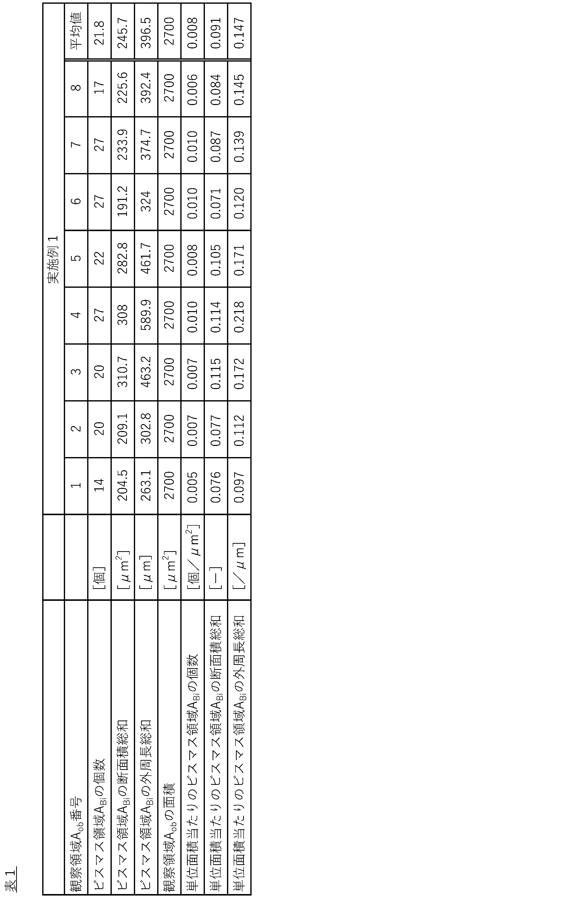
プリント配線板1を、ビア30の断面が露出するように樹脂基材10に対して垂直な方向に切断し、ビア30の断面の任意の8か所について、走査型電子顕微鏡を用いて、反射電子像を得た。測定の条件は、出力15kV、測定倍率900倍とした。得られた各画像について、画像サイズ588×441ピクセル=60×45μmの視野を観察領域Aobとして、画像解析ソフト(製品名「ImageJ Ver.1.52」、National Institute of Health社製)を用いて、画像解析を行った。この際、256段階に分けられた濃淡の下限を150、上限を175に設定することで、二値化処理を行った。このような閾値を設定することで、ビスマスを主成分とするビスマス領域ABiを検出することができた。二値化処理によって検出された各ビスマス領域ABiの外周長[μm]および断面積[μm2]を画像解析により求めた。さらに、各ビスマス領域31の外周長の総和[μm]を観察領域Aobの面積[μm2]で除することにより、ビア30の断面の単位面積当たりのビスマス領域31の外周長の総和[/μm]を求めた。同様に、各ビスマス領域ABiの断面積の総和[μm2]を観察領域Aobの面積[μm2]で除することにより、ビア30の断面の単位面積当たりのビスマス領域31の断面積の総和[-]を求めた。さらに、二値化により検出されたビスマス領域ABiの個数を数え、観察領域Aobの面積[μm2]で除することにより、ビア30の断面の単位面積当たりのビスマス領域31の個数[個/μm2]を求めた。このようにして8つの観察領域Aobについてそれぞれ単位面積当たりのビスマス領域の外周長の総和、断面積の総和、および個数を求め、これらの平均値を求めた。結果を表1に示す。図5(a)に実施例1のプリント配線板1のビア30の断面の走査型電子顕微鏡による反射電子像を示し、図5(b)に、プリント配線板1の図5(a)と同一の視野における二値化処理後の画像を示す。
得られたプリント配線板1を試験サンプルとした複数の試験サンプルについて、温度サイクル試験器装置(製品名「WINTECH」、 ETAC社製)を用いて、熱衝撃試験を行った。試験条件は、温度範囲-40~+85℃、試験時間30分、サイクル数を250、500、750、1000とした。250サイクルごとに、不良率の発生率を測定した。不良率とは、抵抗値不良が発生した試験サンプルの割合である。結果を表3に示す。
導電性ペーストにおける半田粉と銅粉の配合比を、半田粉/銅粉の重量比で1.1,1.2,1.4にそれぞれ変更した以外は、実施例1と同様にしてプリント配線板1を得た。得られたプリント配線板1について、実施例1と同様に、ビスマス領域31の外周長、断面積、および個数の評価を行ったところ、いずれもプリント配線板1においても、ビア断面の単位面積当たりのビスマス領域31の外周長の総和が0.25/μm以下であり、ビア断面の単位面積当たりのビスマス領域31の断面積の総和が0.10下であり、ビア断面の単位面積当たりのビスマス領域31の個数が0.01個/μm2以下であった。また、これらのプリント配線板1について、熱衝撃試験を行った。結果を表3に示す。
導電性ペーストに含まれる銅粉として、拡散阻害元素を含まないものを使用した以外は、実施例1と同様にしてプリント配線板1を得て、実施例1と同様にビア30の断面の評価、および熱衝撃試験を行った。結果を表2および表3に示す。図6(a)に、比較例1のプリント配線板のビアの断面の走査型電子顕微鏡による反射電子像を示し、図6(b)に、比較例1のプリント配線板の図6(a)と同一の視野における二値化処理後の画像を示す。


10…樹脂基材
20…電極
30…ビア
31…ビスマス領域
32…高融点金属領域
33…樹脂領域
40…接着層
Claims (6)
- プリント配線板であって、
絶縁層と、
前記絶縁層上に設けられた導体層と、
前記絶縁層を貫通し、前記導体層と電気的に接続されたビアと、を備え、
前記ビアは、ビスマスを主成分とするビスマス領域を含み、
前記ビアの断面の単位面積当たりの前記ビスマス領域の外周長の総和が0.25/μm以下であるプリント配線板。 - 請求項1に記載のプリント配線板であって、
前記ビアの断面の単位面積当たりの前記ビスマス領域の断面積の総和が0.10以下であるプリント配線板。 - 請求項1または2に記載のプリント配線板であって、
前記ビアの断面の単位面積当たりの前記ビスマス領域の個数が0.01個/μm2以下であるプリント配線板。 - 請求項1~3のいずれかに記載のプリント配線板であって、
前記ビアは、SnBiを含む半田粉と、銅を主成分とする金属粉を用いて形成されたものであり、
前記半田粉と前記金属粉との配合比が、重量比(半田粉/金属粉)で、0.5~2.0であるプリント配線板。 - プリント配線板であって、
絶縁層と、
前記絶縁層上に設けられた電極と、
前記絶縁層を貫通し、前記電極と電気的に接続されたビアと、を備え、
前記ビアは、ビスマスを主成分とする球状のビスマス領域を含むプリント配線板。 - 請求項5に記載のプリント配線板であって、
前記ビスマス領域の断面の平均径が4μm以上であるプリント配線板。
Priority Applications (2)
| Application Number | Priority Date | Filing Date | Title |
|---|---|---|---|
| EP23900544.0A EP4633298A1 (en) | 2022-12-06 | 2023-11-29 | Printed wiring board |
| JP2024562722A JPWO2024122429A1 (ja) | 2022-12-06 | 2023-11-29 |
Applications Claiming Priority (2)
| Application Number | Priority Date | Filing Date | Title |
|---|---|---|---|
| JP2022195201 | 2022-12-06 | ||
| JP2022-195201 | 2022-12-06 |
Publications (1)
| Publication Number | Publication Date |
|---|---|
| WO2024122429A1 true WO2024122429A1 (ja) | 2024-06-13 |
Family
ID=91379182
Family Applications (1)
| Application Number | Title | Priority Date | Filing Date |
|---|---|---|---|
| PCT/JP2023/042781 Ceased WO2024122429A1 (ja) | 2022-12-06 | 2023-11-29 | プリント配線板 |
Country Status (3)
| Country | Link |
|---|---|
| EP (1) | EP4633298A1 (ja) |
| JP (1) | JPWO2024122429A1 (ja) |
| WO (1) | WO2024122429A1 (ja) |
Cited By (1)
| Publication number | Priority date | Publication date | Assignee | Title |
|---|---|---|---|---|
| WO2025254165A1 (ja) * | 2024-06-04 | 2025-12-11 | 株式会社フジクラ | プリント配線板 |
Citations (3)
| Publication number | Priority date | Publication date | Assignee | Title |
|---|---|---|---|---|
| JP5099272B1 (ja) | 2011-12-26 | 2012-12-19 | パナソニック株式会社 | 多層配線基板とその製造方法 |
| WO2016136204A1 (ja) * | 2015-02-27 | 2016-09-01 | タツタ電線株式会社 | 導電性ペースト及びこれを用いた多層基板 |
| JP2020053524A (ja) * | 2018-09-26 | 2020-04-02 | 日亜化学工業株式会社 | 回路基板及び部品実装基板、並びに、それらの製造方法 |
-
2023
- 2023-11-29 JP JP2024562722A patent/JPWO2024122429A1/ja active Pending
- 2023-11-29 EP EP23900544.0A patent/EP4633298A1/en active Pending
- 2023-11-29 WO PCT/JP2023/042781 patent/WO2024122429A1/ja not_active Ceased
Patent Citations (3)
| Publication number | Priority date | Publication date | Assignee | Title |
|---|---|---|---|---|
| JP5099272B1 (ja) | 2011-12-26 | 2012-12-19 | パナソニック株式会社 | 多層配線基板とその製造方法 |
| WO2016136204A1 (ja) * | 2015-02-27 | 2016-09-01 | タツタ電線株式会社 | 導電性ペースト及びこれを用いた多層基板 |
| JP2020053524A (ja) * | 2018-09-26 | 2020-04-02 | 日亜化学工業株式会社 | 回路基板及び部品実装基板、並びに、それらの製造方法 |
Non-Patent Citations (1)
| Title |
|---|
| See also references of EP4633298A1 |
Cited By (1)
| Publication number | Priority date | Publication date | Assignee | Title |
|---|---|---|---|---|
| WO2025254165A1 (ja) * | 2024-06-04 | 2025-12-11 | 株式会社フジクラ | プリント配線板 |
Also Published As
| Publication number | Publication date |
|---|---|
| JPWO2024122429A1 (ja) | 2024-06-13 |
| EP4633298A1 (en) | 2025-10-15 |
Similar Documents
| Publication | Publication Date | Title |
|---|---|---|
| JP5382270B1 (ja) | 配線基板とその製造方法 | |
| JP5349703B1 (ja) | はんだ合金、ソルダペーストおよび電子回路基板 | |
| EP2617515B1 (en) | Semiconductor device bonding material | |
| JP6766960B2 (ja) | 多層配線基板、電子機器、及び、多層配線基板の製造方法 | |
| US8920580B2 (en) | Solder paste and electronic device | |
| TWI432103B (zh) | A wiring substrate, a method for manufacturing a wiring substrate, and a through-hole paste | |
| DE69321660T2 (de) | Diffusionsverbindungsverfahren | |
| CN102884872B (zh) | 多层布线基板、多层布线基板的制造方法 | |
| JP4859999B1 (ja) | 多層配線基板、多層配線基板の製造方法、及びビアペースト | |
| TWI393496B (zh) | 配線基板、配線基板的製造方法及通孔糊 | |
| CN104246909B (zh) | 导电浆料、固化物、电极以及电子设备 | |
| US20140124250A1 (en) | Wiring board and method for manufacturing same | |
| KR20140107405A (ko) | 전자부품 | |
| WO2013132942A1 (ja) | 接合方法、接合構造体およびその製造方法 | |
| WO2024122429A1 (ja) | プリント配線板 | |
| JP4949802B2 (ja) | 導電性ペースト及びこれを用いた多層基板 | |
| TWI747537B (zh) | 芯材料、電子部件以及凸塊電極的形成方法 | |
| KR20190045846A (ko) | 핵재료 및 납땜 이음 및 범프 전극의 형성 방법 | |
| JP2017130623A (ja) | 充填用ペースト材料、それを用いたビアホール導体の製造方法および多層基板の製造方法 | |
| JP2009224059A (ja) | 導電性微粒子、異方性導電材料、及び、接続構造体 | |
| WO2025254165A1 (ja) | プリント配線板 | |
| JP6543890B2 (ja) | 高温はんだ合金 | |
| JP2009224058A (ja) | 導電性微粒子、異方性導電材料、及び、接続構造体 | |
| JP2003224339A (ja) | 導体ペーストおよびこれを用いた配線基板 | |
| JP2015065333A (ja) | セラミック電子部品 |
Legal Events
| Date | Code | Title | Description |
|---|---|---|---|
| 121 | Ep: the epo has been informed by wipo that ep was designated in this application |
Ref document number: 23900544 Country of ref document: EP Kind code of ref document: A1 |
|
| WWE | Wipo information: entry into national phase |
Ref document number: 2024562722 Country of ref document: JP |
|
| WWE | Wipo information: entry into national phase |
Ref document number: 2023900544 Country of ref document: EP |
|
| NENP | Non-entry into the national phase |
Ref country code: DE |
|
| ENP | Entry into the national phase |
Ref document number: 2023900544 Country of ref document: EP Effective date: 20250707 |
|
| WWP | Wipo information: published in national office |
Ref document number: 2023900544 Country of ref document: EP |