WO2024142555A1 - 情報処理装置 - Google Patents
情報処理装置 Download PDFInfo
- Publication number
- WO2024142555A1 WO2024142555A1 PCT/JP2023/037435 JP2023037435W WO2024142555A1 WO 2024142555 A1 WO2024142555 A1 WO 2024142555A1 JP 2023037435 W JP2023037435 W JP 2023037435W WO 2024142555 A1 WO2024142555 A1 WO 2024142555A1
- Authority
- WO
- WIPO (PCT)
- Prior art keywords
- data
- hash value
- erasure
- storage area
- information processing
- Prior art date
- Legal status (The legal status is an assumption and is not a legal conclusion. Google has not performed a legal analysis and makes no representation as to the accuracy of the status listed.)
- Ceased
Links
Images














Classifications
-
- G—PHYSICS
- G06—COMPUTING OR CALCULATING; COUNTING
- G06F—ELECTRIC DIGITAL DATA PROCESSING
- G06F21/00—Security arrangements for protecting computers, components thereof, programs or data against unauthorised activity
- G06F21/70—Protecting specific internal or peripheral components, in which the protection of a component leads to protection of the entire computer
- G06F21/78—Protecting specific internal or peripheral components, in which the protection of a component leads to protection of the entire computer to assure secure storage of data
-
- G—PHYSICS
- G06—COMPUTING OR CALCULATING; COUNTING
- G06F—ELECTRIC DIGITAL DATA PROCESSING
- G06F21/00—Security arrangements for protecting computers, components thereof, programs or data against unauthorised activity
- G06F21/60—Protecting data
- G06F21/62—Protecting access to data via a platform, e.g. using keys or access control rules
-
- G—PHYSICS
- G06—COMPUTING OR CALCULATING; COUNTING
- G06F—ELECTRIC DIGITAL DATA PROCESSING
- G06F21/00—Security arrangements for protecting computers, components thereof, programs or data against unauthorised activity
- G06F21/60—Protecting data
- G06F21/64—Protecting data integrity, e.g. using checksums, certificates or signatures
-
- G—PHYSICS
- G06—COMPUTING OR CALCULATING; COUNTING
- G06F—ELECTRIC DIGITAL DATA PROCESSING
- G06F21/00—Security arrangements for protecting computers, components thereof, programs or data against unauthorised activity
- G06F21/70—Protecting specific internal or peripheral components, in which the protection of a component leads to protection of the entire computer
- G06F21/78—Protecting specific internal or peripheral components, in which the protection of a component leads to protection of the entire computer to assure secure storage of data
- G06F21/79—Protecting specific internal or peripheral components, in which the protection of a component leads to protection of the entire computer to assure secure storage of data in semiconductor storage media, e.g. directly-addressable memories
-
- G—PHYSICS
- G06—COMPUTING OR CALCULATING; COUNTING
- G06F—ELECTRIC DIGITAL DATA PROCESSING
- G06F2221/00—Indexing scheme relating to security arrangements for protecting computers, components thereof, programs or data against unauthorised activity
- G06F2221/21—Indexing scheme relating to G06F21/00 and subgroups addressing additional information or applications relating to security arrangements for protecting computers, components thereof, programs or data against unauthorised activity
- G06F2221/2143—Clearing memory, e.g. to prevent the data from being stolen
Definitions
- This disclosure relates to an information processing device, an information processing method, an information processing system, and a program.
- Patent Document 1 and Non-Patent Document 1 disclose methods for verifying data erasure.
- the current data stored in the storage device after the erasure (e.g., pattern data or random data overwritten onto the original data) is compared with the original data stored in the storage device before the erasure.
- a large amount of data is compared, which places a large load on the information processing device. Therefore, there is a need to verify whether data has been successfully erased with a smaller load than before.
- the present disclosure provides an information processing device, an information processing method, an information processing system, and a program that can verify whether data stored in a storage device has been successfully erased with less load than conventional methods.
- an information processing device it is possible to verify whether data stored in a storage device has been successfully erased with less load than in the past.
- FIG. 1 is a block diagram showing a configuration of an information processing device 1 according to a first embodiment.
- 2 is a block diagram showing a configuration of a storage device 13 in FIG. 1 .
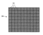
- FIG. 3 is a schematic diagram showing logical blocks 31 of the flash memory 24 of FIG. 2, illustrating an example of an arrangement of the logical blocks 31 that are compared to verify the erasure of data.
- 13 is a flowchart showing an erasing process according to a first comparative example.
- 11 is a flowchart showing an erasing process according to a second comparative example.
- 2 is a flowchart showing an erasure process according to the first embodiment, which is executed by an erasure controller 14 of FIG. 1 .
- FIG. 1 is a table comparing verification methods according to Comparative Example 1, Comparative Example 2, and Example 1.
- FIG. 3 is a schematic diagram showing logical blocks 31 of the flash memory 24 of FIG. 2, illustrating a first modified arrangement of logical blocks 31 that are compared to verify the erasure of data;
- FIG. 3 is a schematic diagram showing logical blocks 31 of the flash memory 24 of FIG. 2, illustrating a second modified arrangement of logical blocks 31 that are compared to verify the erasure of data.
- 10 is a flowchart showing an erasure process according to a second embodiment, which is executed by an erasure controller 14 of FIG. 1;
- 10 is a flowchart showing an erasure process according to a third embodiment, which is executed by an erasure controller 14 of FIG. 1 .
- FIG. 1 is a table comparing verification methods according to Comparative Example 1, Comparative Example 2, and Example 1.
- FIG. 3 is a schematic diagram showing logical blocks 31 of the flash memory 24 of FIG. 2, illustrating a first modified arrangement
- FIG. 17; 18 is a diagram showing an example of an image indicating the progress of data erasure, which is displayed on the display device 18 of FIG. 1 by executing the erasure process of FIG. 17.
- FIG. 18 is a diagram showing another example of an image showing the progress of data erasure, which is displayed on the display device 18 of FIG. 1 by executing the erasure process of FIG. 17.
- FIG. 11 is a block diagram showing a configuration of an information processing system including an information processing device 1 and a server device according to a third embodiment.
- FIG. 27 is a block diagram showing the configuration of the server device 2 of FIG. 26.
- 27 is a flowchart showing an erasure process executed by the server device 2 of FIG. 26.
- 27 is a flowchart showing an erasure process executed by the information processing device 1 of FIG. 26 .
- 27 is a flowchart showing a modified example of the erasure process executed by the server device 2 of FIG. 26 .
- 27 is a flowchart showing a modified example of the erasure process executed by the information processing device 1 of FIG. 26 .
- 32 is a flowchart showing a subroutine of the pre-processing (step S231) of FIG. 31 .
- 32 is a flowchart showing a subroutine of the key change process (step S232) of FIG. 31.
- 32 is a flowchart showing a subroutine
- the CPU 11 controls the operation of the entire information processing device 1.
- RAM 12 temporarily stores programs and data necessary for the operation of information processing device 1.
- the storage device 13 stores data including an operating system, application programs, and user data.
- the storage device 13 is a self-encrypting drive (SED) that has a function of self-encrypting the data stored therein, for example, a solid-state drive (SSD) that has a self-encrypting function.
- SSD solid-state drive
- the non-volatile memory 15 stores the programs and data necessary to execute the erasure process.
- the non-volatile memory 15 includes a non-volatile storage medium such as a flash memory.
- the communication device 16 is connected to other external information processing devices so as to be able to communicate with them via a communication line such as a local area network (LAN).
- LAN local area network
- the input device 17 receives user input that controls the operation of the information processing device 1.
- the input device 17 includes, for example, a keyboard and a pointing device.
- the display device 18 displays information related to the state of the information processing device 1, for example, information related to the erasure of data stored in the storage device 13.
- the CPU 11, RAM 12, storage device 13, erasure controller 14, non-volatile memory 15, communication device 16, input device 17, and display device 18 are connected to each other via bus 10.
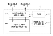
- FIG. 2 is a block diagram showing the configuration of the storage device 13 in FIG. 1.
- the storage device 13 includes an input/output controller 21, a random access memory (RAM) 22, a non-volatile memory 23, and a flash memory 24.
- the input/output controller 21 controls the writing and reading of data to the storage device 13.
- the RAM 22 is a buffer memory that temporarily stores data to be written to the storage device 13 and data to be read from the storage device 13.
- the non-volatile memory 23 stores a firmware program (FW) and an encryption key for the storage device 13.
- the flash memory 24 is a non-volatile storage medium having a storage area.
- the input/output controller 21 controls the operation of the storage device 13 by executing the firmware program stored in the non-volatile memory 23.
- the input/output controller 21 writes input data to the storage area of the flash memory 24, and outputs data read from the storage area.
- the storage device 13 has a self-encryption function.
- the storage device 13 may encrypt and decrypt data stored in the entire storage area of the flash memory 24, or may encrypt and decrypt only data stored in a part of the storage area.
- the input/output controller 21 encrypts at least a portion of the data to be written to the storage area of the flash memory 24 using an encryption key stored in the non-volatile memory 23.
- the input/output controller 21 also decrypts at least a portion of the data read from the storage area of the flash memory 24 using the encryption key.
- the input/output controller 21 may use hardware, software, or a combination thereof to encrypt and decrypt data.
- a storage device 13 with a self-encrypting function when the encryption key is changed, data encrypted with the previous encryption key and stored in the storage area of the flash memory 24 cannot be decrypted using the changed encryption key. Therefore, by changing the encryption key of the storage device 13, the original data stored in the storage device 13 becomes inaccessible, and equivalently, the original data stored in the storage device 13 can be erased (cryptographically erased).
- the input/output controller 21 changes the encryption key stored in the non-volatile memory 23 under the control of the erase controller 14.
- the encryption key may be changed, for example, by the input/output controller 21 executing a revert command included in the firmware of the storage device 13.
- the erasure controller 14 compares the current data stored in the storage device 13 after the encryption key is changed with the original data that was stored in the storage device 13 before the encryption key was changed. If the current data differs from the original data, the erasure controller 14 determines that the data has been successfully erased, and if the current data matches the original data, the erasure controller 14 determines that the data has not been erased.
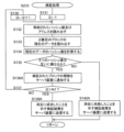
- FIG. 4 is a flowchart showing the erasure process according to Comparative Example 1.
- FIG. 4 shows the method of verifying data erasure disclosed in Non-Patent Document 1.
- the erasure process in FIG. 4 and other figures is started, for example, when an instruction to erase data stored in the storage device 13 is issued via the BIOS or UEFI program.
- step S1 the erase controller 14 reads the original data of the specified logical block 31 as shown in FIG. 3.
- the "original data” refers to the data read from the specified logical block 31 of the storage area when the encryption key before the change is stored in the non-volatile memory 23. If this logical block 31 is the target of encryption and decryption, the erase controller 14 obtains the data decrypted using the encryption key before the change. On the other hand, if this logical block 31 is not the target of encryption and decryption, the erase controller 14 obtains the data read from the logical block 31 as is without decrypting it.
- step S4 the erase controller 14 reads the current data of the specified logical block 31, the same as in step S1.
- current data refers to the data read from the specified logical block 31 of the storage area when the changed encryption key is stored in the non-volatile memory 23. If this logical block 31 is to be encrypted and decrypted, the erase controller 14 obtains data decrypted using the changed encryption key. On the other hand, if this logical block 31 is not to be encrypted or decrypted, the erase controller 14 obtains the data read from the logical block 31 without decrypting it.
- step S5 the erasure controller 14 receives the temporarily saved original data from the external information processing device.
- step S6 the erase controller 14 determines whether the current data is different from the original data, and if YES, proceeds to step S7, and if NO, proceeds to step S8.
- the current data and the original data are compared for each logical block 31, so this can be performed using a RAM 12 with a size of several GB to several tens of GB.
- step S7 the erasure controller 14 outputs to the display device 18 a verification result indicating that the data erasure was successful.
- step S8 the erasure controller 14 outputs to the display device 18 a verification result indicating that the data erasure was unsuccessful.
- the process in FIG. 4 involves comparing a large amount of data that cannot be stored in the RAM 12, so an external information processing device is required to temporarily save the data. Therefore, there is a need for a method of verifying data erasure that does not require an external information processing device and can be executed only by the information processing device 1.
- FIG. 5 is a flowchart showing the erasure process according to Comparative Example 2.
- FIG. 5 shows the method of verifying data erasure disclosed in Patent Document 1.
- step S11 the erase controller 14 writes known pattern data to a specified logical block 31, for example as shown in FIG. 3.
- the pattern data includes, for example, a bit string consisting of all 1's, a bit string consisting of all 0's, a random bit string, etc.
- the pattern data is pre-stored in the non-volatile memory 15.
- the pattern data is encrypted using the encryption key before the change and written to the specified logical block 31 of the storage area.
- the erasure controller 14 may determine that data erasure has been successful even if the hash values match in several logical blocks 31. Furthermore, if the hash values differ in more than half of the logical blocks 31, the erasure controller 14 may determine that data erasure has been successful.
- data of one logical block 31 for every 10 blocks may be specified.
- data of one logical block 31 for every 20 blocks may be specified.
- the storage area is divided into 10,000 logical blocks 31 and 10% of the storage area, i.e., data of 1,000 logical blocks 31, is read and verified, the hash value of the data has a total size of 32 KB.
- the storage area is divided into 1,000 logical blocks 31 and 10% of the storage area, i.e., data of 100 logical blocks 31, is read and verified, the hash value of the data has a total size of 3,200 bytes.
- the addresses of the logical blocks 31 must also be stored.
- the address (0 to 9999 or 0 to 999) of each logical block 31 is expressed in 2 bytes. Therefore, when reading and verifying data from 1,000, 500, 100, or 50 logical blocks 31, the total size of the stored addresses will be 2,000 bytes, 1,000 bytes, 200 bytes, or 100 bytes. In any case, the size of the stored addresses is relatively small.
- the memory area of the storage device 13 is not limited to two partial areas 24a-1 to 24a-2, but may be divided into three or more partial areas.
- step S31 the erase controller 14 reads the original data of the specified logical block 31, for example, as shown in FIG. 3, FIG. 8, or FIG. 9.
- step S32 the erase controller 14 calculates a hash value of the original data.
- One hash value may be calculated for each logical block 31, or one hash value may be calculated for a predetermined number of logical blocks 31.
- a buffer memory for storing the read data is provided in the RAM 12.
- the buffer memory has, for example, a size ten times that of the logical block 31.
- the erase controller 14 writes the read data sequentially to the buffer memory, and calculates the hash value of the data when the buffer memory becomes full. Since the power supply of the information processing device 1 is not turned off during the execution of the process of FIG. 10 (particularly before and after the encryption key is changed), the calculated hash value may be stored in the RAM 12.
- the calculated hash value may also be stored in the non-volatile memory 15.
- step S34 the erasure controller 14 reads the current data of the same specified logical block 31 as in step S31. Then, in step S35, the erasure controller 14 calculates a hash value of the current data using the same hash function as that used to calculate the hash value of the original data. As in the case of calculating the hash value of the original data, one hash value may be calculated for each logical block 31, or one hash value may be calculated for a predetermined number of logical blocks 31. In this way, for the same one or more logical blocks 31, the hash value of the original data is calculated (step S32), and the hash value of the current data is calculated (step S35).
- writing data takes longer than reading data.
- the processing time can be reduced compared to the case in FIG. 6.
- the amount of calculation is reduced compared to when one hash value is calculated for each logical block 31, improving processing speed and reducing the memory capacity required to store the calculated hash values.
- FIG. 11 is a flowchart showing an erasure process according to the third embodiment, which is executed by the erasure controller 14 of FIG.
- FIG. 12 is a schematic diagram showing the logical blocks 31 of the flash memory 24 of FIG. 2, and shows a case where all the logical blocks 31 are compared to verify the erasure of data.
- FIG. 13 is a schematic diagram showing the logical blocks 31 of the flash memory 24 of FIG. 2, and shows a case where the logical blocks 31 included in each of the partial areas 24b-1 and 24b-2 are compared to verify the erasure of data.
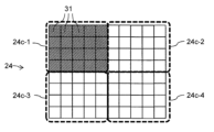
- FIG. 14 is a schematic diagram showing the logical blocks 31 of the flash memory 24 of FIG. 2, and shows a case where the logical blocks 31 included in each of the partial areas 24c-1 to 24c-4 are compared to verify the erasure of data.
- FIG. 15 is a schematic diagram showing the logical blocks 31 of the flash memory 24 of FIG.
- the entire storage area is divided into eight partial areas 24d-1 to 24d-8, and one hash value is calculated for each of the partial areas 24d-1 to 24d-8. As in the cases of FIGS. 12 to 15, a hash value may be calculated for each of the further divided partial areas.
- step S43 of FIG. 11 the erasure controller 14 changes the encryption key stored in the non-volatile memory 23.
- step S44 the erasure controller 14 reads the current data in the storage area. Then, in step S45, the erasure controller 14 calculates a hash value of the entire current data in the storage area.
- step S47 the erasure controller 14 determines whether or not a comparison has been made with all hash values of the original data calculated in step S42. If YES, the process proceeds to step S50; if NO, the process proceeds to step S48.
- step S49 the erasure controller 14 outputs to the display device 18 a verification result indicating that the data erasure was successful.
- step S50 the erasure controller 14 outputs to the display device 18 a verification result indicating that the data erasure was unsuccessful.
- the collision of hash values may be avoided by comparing the hash values of smaller partial areas.
- Fig. 16 is a block diagram showing the configuration of an information processing device 1A according to a modified example of the first embodiment.
- the information processing device 1A further includes a device interface (I/F) 19 for connecting to an external device.
- the device interface 19 is, for example, a USB.
- the device interface 19 is connected to an external storage device 41 such as a USB memory, a solid state drive, or a hard disk drive.
- the calculated hash value of the original data may be stored in the external storage device 41 instead of being stored in the RAM 12 or the non-volatile memory 15. Since it is difficult to infer the original data from the hash value, even if the external storage device 41 is lost or stolen, there is a low possibility that confidential data will be leaked.
- the calculated hash value of the original data may be transmitted to and stored in an external information processing device connected via the communication device 16.
- the information processing device 1, 1A may further include a drive device for a storage medium such as a CD or DVD, in which case the calculated hash value of the original data may be stored on a CD, DVD, or the like.
- the storage area may include a plurality of partial areas obtained by logically dividing the storage area, each of which includes a plurality of logically contiguous blocks.
- the erasure controller 14 designates, for each of the plurality of partial areas, a different proportion of logical blocks from the plurality of logical blocks included in the partial area.
- the first and second hash values are calculated based on the data stored in the designated plurality of blocks.
- the storage area may include multiple blocks.
- the first and second hash values are calculated based on data stored in multiple blocks that are logically adjacent to each other.
- the storage area may include a plurality of partial areas obtained by logically dividing the storage area into a plurality of sizes different from each other.
- the first hash value is calculated for each of the plurality of partial areas having a plurality of sizes based on the data stored in the partial area.
- the erasure controller 14 calculates a second hash value for each of the plurality of partial areas having a first size among the plurality of sizes based on the data stored in the partial area. If the second hash value for the partial area having the first size is different from the first hash value, the erasure controller 14 outputs a verification result indicating that the data stored in the storage device 13 has been successfully erased.
- the information processing method includes a step of outputting a verification result indicating that erasure of the data stored in the storage device 13 was successful if the second hash value is different from the first hash value.
- the information processing method includes a step of outputting a verification result indicating that erasure of the data stored in the storage device 13 was unsuccessful if the second hash value matches the first hash value.
- step S115 the erasure controller 14 outputs the number of logical blocks 31 for which the processing of steps S112 to S114 has been executed to the display device 18 in a predetermined format.
- step S122 the erasure controller 14 outputs to the display device 18 in a specified format a message indicating that the encryption key change has been completed.
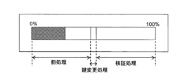
- FIG. 21 is a diagram showing an example of an image showing the progress of data erasure, displayed on the display device 18 of FIG. 1 by executing the erasure process of FIG. 17.
- FIG. 21(a) is an image showing the progress of preprocessing.
- the progress of preprocessing is represented, for example, by a progress bar showing the ratio of the number of processed logical blocks 31 to the number of specified logical blocks 31, i.e., i1/N1.
- FIG. 21(b) is an image showing the progress of key change processing.
- the progress of key change processing is represented, for example, by a progress bar showing whether the change of the encryption key has been completed.
- FIG. 21(c) is an image showing the progress of verification processing.
- the progress of verification processing is represented, for example, by a progress bar showing the ratio of the number of verified logical blocks 31 to the number of specified logical blocks 31, i.e., i2/N1.
- FIG. 24 is a flowchart showing a second modified example of the verification process of FIG. 17.
- the process of FIG. 24 includes steps S151 to S156 in addition to the steps of FIG. 20.
- parameter j2 increases or decreases depending on whether the hash values match or mismatch. Therefore, if hash value collisions occur consecutively in several of the specified logical blocks 31 that are close to each other, parameter j2 increases. In this case, it is considered that the storage area containing these logical blocks 31 is not subject to encryption, and the data is stored in plain text. On the other hand, if hash value matches and mismatches occur almost alternately in several of the specified logical blocks 31 that are close to each other, parameter j2 does not increase. In this case, the hash value collisions are considered to be accidental.
- step S162 the erasure controller 14 initializes parameters i3 and i4 to 1, and parameter j3 to 0.
- the number of collisions of hash values is counted in a group of a predetermined number of logical blocks 31 that are close to each other among the specified logical blocks 31.
- Parameter i3 indicates the position of the group of logical blocks 31.
- the number of collisions of hash values in a certain group is counted using parameter j3.
- step S163 the erasure controller 14 determines whether the hash value of the current data in the i3+i4th logical block 31 matches the hash value of the original data based on the address stored in step S161, and if YES, proceeds to step S164, and if NO, proceeds to step S165.
- step S164 the erasure controller 14 increments the parameter j3 by 1.
- step S165 the erasure controller 14 determines whether the parameter i4 has exceeded the threshold value N4, i.e., whether all logical blocks 31 contained in the current group have been processed; if YES, the process proceeds to step S167; if NO, the process proceeds to step S166.
- step S166 the erasure controller 14 increments parameter i4 by 1 and repeats steps S163 to S165.
- step S167 the erasure controller 14 determines whether the parameter j3 exceeds the threshold value Th3. If YES, the process proceeds to step S140. If NO, the process proceeds to step S168.
- step S168 the erasure controller 14 determines whether the parameter i3 has exceeded the threshold value N3, i.e., whether the group of logical blocks 31 has been shifted to all positions; if YES, the process proceeds to step S139; if NO, the process proceeds to step S169.
- the threshold value Th3 in step S167 may be set to a value close to the number N3 of logical blocks 31 included in the group.
- the erasure controller 14 may calculate j3/N3, in which case the threshold value Th3 may be set to a value close to 1, for example.
- the erasure controller 14 may output the progress of erasure of the data stored in the storage device 13 to the display device 18 .
- information processing devices 1-1 to 1-3 are collectively referred to as "information processing device 1.”
- FIG. 27 is a block diagram showing the configuration of the server device 2 in FIG. 26.
- the server device 2 includes a bus 120, a CPU 121, a RAM 122, a storage device 123, a communication device 126, an input device 127, and a display device 128.
- the CPU 121 controls the operation of the entire server device 2, and also manages the erasure of data stored in the storage device 13 of each information processing device 1.
- the RAM 122 temporarily stores programs and data necessary for the operation of the server device 2.
- the storage device 123 is a non-volatile storage medium that stores programs necessary for the operation of the server device 2.
- the communication device 126 is communicably connected to each information processing device 1 via the communication line 3.
- the input device 127 receives user input that controls the operation of the server device 2.
- the input device 127 includes, for example, a keyboard and a pointing device.
- the display device 128 displays information related to the erasure of data stored in the storage device 13 of each information processing device 1.
- the CPU 121, RAM 122, storage device 123, communication device 126, input device 127, and display device 128 are connected to each other via a bus 120.
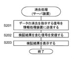
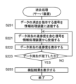
- step S201 of FIG. 28 the CPU 121 of the server device 2 transmits a control signal to the information processing device 1 to instruct the data to be erased.
- step S211 of FIG. 29 the erasure controller 14 of the information processing device 1 receives a control signal from the server device 2 instructing the data erasure.
- the erasure controller 14 executes steps S212 to S219 in accordance with the control signal.
- Steps S212 to S217 are the same as steps S31 to S36 of FIG. 10. If it is determined in step S217 that the hash value of the current data is different from the hash value of the original data, the process proceeds to step S218; otherwise, the process proceeds to step S219.
- step S218 the erasure controller 14 transmits a notification signal including a verification result indicating that the data erasure was successful to the server device 2.
- step S219 the erasure controller 14 transmits a notification signal including a verification result indicating that the data erasure was unsuccessful to the server device 2.
- step S202 of FIG. 28 the CPU 121 of the server device 2 receives a notification signal indicating the verification result from the information processing device 1.
- step S203 the CPU 121 outputs the verification result to the display device 128.
- the deletion of data stored in the storage devices 13 of multiple information processing devices 1 can be centrally controlled by the server device 2, and it is also possible to verify with a small load whether the data deletion was successful.
- the progress of data erasure may be output to the display device 128 of the server device 2.
- FIG. 30 is a flowchart showing a modified example of the erasure process executed by the server device 2 of FIG. 26.
- FIG. 31 is a flowchart showing a modified example of the erasure process executed by the information processing device 1 of FIG. 26.
- the process of FIG. 30 includes steps S221 to S223 instead of step S202 of FIG. 28.
- the process of FIG. 31 includes steps S231 to S233 instead of steps S212 to S219 of FIG. 29.
- step S201 of FIG. 30 the CPU 121 of the server device 2 sends a control signal to the information processing device 1 to instruct the data to be erased.
- step S211 of FIG. 31 the erasure controller 14 of the information processing device 1 receives a control signal from the server device 2 instructing the data erasure.
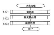
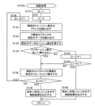
- the erasure controller 14 executes steps S231 to S233 in accordance with the control signal. Steps S231 to S233 are similar to steps S101 to S103 of FIG. 17, except that the progress of the data erasure and the verification results are sent to the server device 2 instead of being output to the display device 18 of the information processing device 1.
- FIG. 32 is a flowchart showing a subroutine of the pre-processing (step S231) of FIG. 31.
- the process of FIG. 32 includes step S115A instead of step S115 of FIG. 18.
- the erasure controller 14 transmits a notification signal to the server device 2, which includes the number of logical blocks 31 for which the processes of steps S112 to S114 have been executed, as the progress of the data erasure.
- FIG. 33 is a flowchart showing a subroutine of the key change process (step S232) of FIG. 31.
- the process of FIG. 33 includes step S122A instead of step S122 of FIG. 19.
- the erasure controller 14 transmits a notification signal to the server device 2 indicating that the encryption key change has been completed as the progress of the data erasure.
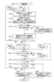
- FIG. 34 is a flowchart showing a subroutine of the verification process (step S233) of FIG. 31.
- the process of FIG. 34 includes steps S136A, S139A, and S140A instead of steps S136, S139, and S140 of FIG. 20.
- step S136A the erasure controller 14 transmits a notification signal including the number of verified logical blocks 31 as the progress of data erasure to the server device 2.
- step S139A the erasure controller 14 transmits a notification signal including a verification result indicating that data erasure was successful to the server device 2.
- the erasure controller 14 transmits a notification signal including a verification result indicating that data erasure was unsuccessful to the server device 2.
- step S221 of FIG. 30 the CPU 121 of the server device 2 receives a notification signal including the progress of data erasure from the information processing device 1.
- step S222 the CPU 121 outputs the progress of data erasure to the display device 128 in a predetermined format, similar to when outputting to the display device 18 of the information processing device 1.
- step S223 the CPU 121 determines whether or not data erasure has been completed, i.e., whether or not a notification signal indicating a verification result has been received from the information processing device 1; if YES, the process proceeds to step S203; if NO, the process returns to step S221.
- step S203 the CPU 121 outputs the verification result to the display device 128.
- the information processing system 100 according to the third embodiment includes the information processing device 1 according to the first embodiment, and a server device 2 connected via a communication line to the information processing device 1.
- An erasure controller 14 controls erasure of data stored in the storage device 13 in accordance with a control signal received from the server device 2.
- the erasure controller 14 may transmit a first notification signal including the verification result to the server device 2.
- the server device 2 may include a display device 128 that outputs the verification result.
- the erasure controller 14 may transmit a second notification signal including the progress of erasing the data stored in the storage device 13 to the server device 2.
- the display device 128 displays the progress.
- the storage device 13 is not limited to a solid state drive, but may be a non-volatile storage medium such as a hard disk drive (HDD) with a self-encrypting function.
- HDD hard disk drive
- the verification results are not limited to being output to the display device 18, but may also be output to an external information processing device via the communication device 16.
- the erasure controller 14 may always specify the first 32 bytes of the storage area.
- the erasure controller 14 may add a salt (a predetermined keyword) to the data when calculating the hash value.
- the erasure controller 14 may shrink the size of the logical block 31 to, for example, 1/10.
- the components described in the attached drawings and detailed description may include not only components essential for solving the problem, but also components that are not essential for solving the problem in order to illustrate the above technology. Therefore, just because these non-essential components are described in the attached drawings or detailed description, it should not be immediately determined that these non-essential components are essential.
- An information processing device includes: A storage device having a function of self-encrypting data to be stored therein; an erase controller for controlling erasure of data stored in the storage device;
- the storage device includes: A storage medium having a storage area; a non-volatile memory storing an encryption key; an input/output controller that writes input data to the storage area, outputs data read from the storage area, encrypts at least a portion of the data to be written to the storage area using the encryption key, and decrypts at least a portion of the data read from the storage area using the encryption key;
- the erase controller includes: If a first encryption key is stored in the non-volatile memory, obtaining a first hash value calculated based on data to be stored at a specified position in the storage area or based on data stored at a specified position in the storage area; controlling the storage device to change the first encryption key stored in the non-volatile memory to a second encryption key; if the second encryption key is
- An information processing device is the information processing device according to the first aspect, the erase controller controls the storage device to store predetermined pattern data at the specified location in the storage area; The first hash value is calculated based on the pattern data.
- An information processing device is the information processing device according to the first aspect, The erasure controller calculates the first hash value based on data read from the specified location in the storage area.
- An information processing device is the information processing device according to the third aspect, the storage area includes a plurality of blocks; The first and second hash values are calculated for each of a predetermined number of blocks based on the data stored in the blocks.
- An information processing device is an information processing device according to any one of the first to fourth aspects, the storage area includes a plurality of partial areas obtained by logically dividing the storage area, each of the partial areas including a plurality of logically contiguous blocks; the erasure controller designates, for each of the plurality of partial regions, a different ratio of blocks among a plurality of blocks included in the partial region; The first and second hash values are calculated based on data stored in the specified plurality of blocks.
- An information processing device is an information processing device according to any one of the first to fourth aspects, the storage area includes a plurality of blocks; The first and second hash values are calculated based on data stored in a plurality of blocks that are logically adjacent to each other.
- An information processing device is the information processing device according to the first aspect, the storage area includes a plurality of partial areas obtained by logically dividing the storage area into a plurality of partial areas each having a different size; the first hash value is calculated for each of the plurality of partial regions having the plurality of sizes based on data stored in the partial region;
- the erase controller includes: calculating the second hash value for each of a plurality of partial regions having a first size among the plurality of sizes based on data stored in the partial region; outputting a verification result indicating that the data stored in the storage device has been successfully erased if the second hash value is different from the first hash value for the partial area having the first size; if the second hash value matches the first hash value for a partial area having the first size, calculate the second hash value for each of a plurality of partial areas having a second size smaller than the first size among the plurality of sizes based on data stored in the partial area; If the second hash value is different from
- a first display device is provided for outputting the verification result.
- An information processing device is the information processing device according to the eighth aspect,
- the erasure controller outputs a progress of erasure of the data stored in the storage device to the first display device.
- An information processing system includes: An information processing device according to one of the first to ninth aspects; a server device connected to the information processing device via a communication line, The erasure controller controls erasure of data stored in the storage device according to a control signal received from the server device.
- the erasure controller transmits a first notification signal including the verification result to the server device;
- the server device includes a second display device that outputs the verification result.
- the erasure controller transmits a second notification signal to the server device, the second notification signal including a progress of erasure of the data stored in the storage device;
- the second display device displays the progress.
- An information processing method includes: 1. An information processing method for controlling erasure of data stored in a storage device having a self-encrypting function, comprising: The storage device includes: A storage medium having a storage area; a non-volatile memory storing an encryption key; an input/output controller that writes input data to the storage area, outputs data read from the storage area, encrypts at least a portion of the data to be written to the storage area using the encryption key, and decrypts at least a portion of the data read from the storage area using the encryption key; The information processing method includes: obtaining a first hash value calculated based on data to be stored at a specified location in the storage area or based on data stored at a specified location in the storage area when a first encryption key is stored in the non-volatile memory; controlling the storage device to change the first encryption key stored in the non-volatile memory to a second encryption key; if the second encryption key is stored in the non-volatile memory, calculating
- a program including instructions executed by a processor implemented in an information processing device,
- the information processing device further includes a storage device having a self-encryption function for data to be stored therein;
- the storage device includes: A storage medium having a storage area; a non-volatile memory storing an encryption key; an input/output controller that writes input data to the storage area, outputs data read from the storage area, encrypts at least a portion of the data to be written to the storage area using the encryption key, and decrypts at least a portion of the data read from the storage area using the encryption key;
- the instructions cause the processor to: When a first encryption key is stored in the non-volatile memory, obtaining a first hash value calculated based on data to be stored at a specified location in the storage area or based on data stored at a specified location in the storage area; controlling the storage device to change the first encryption key stored in the non-volatile memory to a second encryption key; calculating a second hash value
- An information processing device is useful for verifying whether data stored in a storage device having a self-encrypting function has been successfully erased.
Landscapes
- Engineering & Computer Science (AREA)
- Theoretical Computer Science (AREA)
- Computer Security & Cryptography (AREA)
- Computer Hardware Design (AREA)
- Software Systems (AREA)
- Physics & Mathematics (AREA)
- General Engineering & Computer Science (AREA)
- General Physics & Mathematics (AREA)
- Health & Medical Sciences (AREA)
- Bioethics (AREA)
- General Health & Medical Sciences (AREA)
- Storage Device Security (AREA)
Abstract
Description
格納されるデータの自己暗号化機能を有する記憶装置と、
前記記憶装置に格納されたデータの消去を制御する消去コントローラとを備え、
前記記憶装置は、
記憶領域を有する記憶媒体と、
暗号鍵を格納した不揮発性メモリと、
入力されたデータを前記記憶領域に書き込み、前記記憶領域から読み出されたデータを出力し、前記記憶領域に書き込まれるデータの少なくとも一部を前記暗号鍵を用いて暗号化し、前記記憶領域から読み出されたデータの少なくとも一部を前記暗号鍵を用いて復号する入出力コントローラとを備え、
前記消去コントローラは、
前記不揮発性メモリに第1の暗号鍵が格納されている場合、前記記憶領域の指定された位置に格納されるべきデータに基づいて、又は、前記記憶領域の指定された位置に格納されているデータに基づいて計算された第1のハッシュ値を取得し、
前記不揮発性メモリに格納された前記第1の暗号鍵を第2の暗号鍵に変更するように前記記憶装置を制御し、
前記不揮発性メモリに前記第2の暗号鍵が格納されている場合、前記記憶領域の前記指定された位置から読み出されたデータに基づいて第2のハッシュ値を計算し、
前記第2のハッシュ値が前記第1のハッシュ値とは異なる場合、前記記憶装置に格納されたデータの消去に成功したことを示す検証結果を出力し、
前記第2のハッシュ値が前記第1のハッシュ値に一致する場合、前記記憶装置に格納されたデータの消去に失敗したことを示す検証結果を出力する。
[第1の実施形態の構成]
図1は、第1の実施形態に係る情報処理装置1の構成を示すブロック図である。情報処理装置1は、バス10、中央処理装置(CPU)11、ランダムアクセスメモリ(RAM)12、記憶装置13、消去コントローラ14、不揮発性メモリ15、通信装置16、入力装置17、及び表示装置18を備える。
ここで、図4及び図5を参照して、従来技術に係るデータ消去の検証について説明する。説明のため、図1の情報処理装置1が、図4及び図5に示す消去処理を実行する場合を想定する。
図6は、図1の消去コントローラ14によって実行される実施例1に係る消去処理を示すフローチャートである。
図10は、図1の消去コントローラ14によって実行される実施例2に係る消去処理を示すフローチャートである。
図11は、図1の消去コントローラ14によって実行される実施例3に係る消去処理を示すフローチャートである。
図16は、第1の実施形態の変形例に係る情報処理装置1Aの構成を示すブロック図である。情報処理装置1Aは、図1の情報処理装置1の各構成要素に加えて、外部装置に接続するための装置インターフェース(I/F)19をさらに備える。装置インターフェース19は、例えば、USBである。図16の例では、装置インターフェース19は、USBメモリ、ソリッドステートドライブ、ハードディスクドライブなどの外部記憶装置41に接続される。
第1の実施形態に係る情報処理装置1は、格納されるデータの自己暗号化機能を有する記憶装置13と、記憶装置13に格納されたデータの消去を制御する消去コントローラ14とを備える。記憶装置13は、記憶領域を有する記憶媒体と、暗号鍵を格納した不揮発性メモリ23と、入力されたデータを記憶領域に書き込み、記憶領域から読み出されたデータを出力し、記憶領域に書き込まれるデータの少なくとも一部を暗号鍵を用いて暗号化し、記憶領域から読み出されたデータの少なくとも一部を暗号鍵を用いて復号する入出力コントローラ21とを備える。消去コントローラ14は、不揮発性メモリ23に第1の暗号鍵が格納されている場合、記憶領域の指定された位置に格納されるべきデータに基づいて、又は、記憶領域の指定された位置に格納されているデータに基づいて計算された第1のハッシュ値を取得する。消去コントローラ14は、不揮発性メモリ23に格納された第1の暗号鍵を第2の暗号鍵に変更するように記憶装置13を制御する。消去コントローラ14は、不揮発性メモリ23に第2の暗号鍵が格納されている場合、記憶領域の指定された位置から読み出されたデータに基づいて第2のハッシュ値を計算する。消去コントローラ14は、第2のハッシュ値が第1のハッシュ値とは異なる場合、記憶装置13に格納されたデータの消去に成功したことを示す検証結果を出力する。消去コントローラ14は、第2のハッシュ値が第1のハッシュ値に一致する場合、記憶装置13に格納されたデータの消去に失敗したことを示す検証結果を出力する。
第2の実施形態では、第1の実施形態の消去処理(図10を参照)を実行しながら、データ消去の進捗度を表示する場合について説明する。
鍵変更処理:a2
検証処理: a3
鍵変更処理:b2
検証処理: b3/N1
第2の実施形態に係る情報処理装置1によれば、消去コントローラ14は、記憶装置13に格納されたデータの消去の進捗度を表示装置18に出力してもよい。
図26は、第3の実施形態に係る情報処理装置1及びサーバ装置を含む情報処理システムの構成を示すブロック図である。図26の情報処理システムは、複数の情報処理装置1-1~1-3、サーバ装置2、及び通信回線3を含む。各情報処理装置1-1~1-3は、図1の情報処理装置1と同様に構成される。サーバ装置2は、通信回線3を介して各情報処理装置1-1~1-3に接続される。
第3の実施形態に係る情報処理システム100は、第1の実施形態に係る情報処理装置1と、情報処理装置1に通信回線を介して接続されたサーバ装置2とを備える。消去コントローラ14は、サーバ装置2から受信された制御信号に従って、記憶装置13に格納されたデータの消去を制御する。
以上のように、本出願において開示する技術の例示として、実施形態を説明した。しかしながら、本開示における技術は、これに限定されず、適宜、変更、置き換え、付加、省略などを行った実施形態にも適用可能である。また、上記実施形態で説明した各構成要素を組み合わせて、新たな実施形態とすることも可能である。
本開示の第1の態様に係る情報処理装置は、
格納されるデータの自己暗号化機能を有する記憶装置と、
前記記憶装置に格納されたデータの消去を制御する消去コントローラとを備え、
前記記憶装置は、
記憶領域を有する記憶媒体と、
暗号鍵を格納した不揮発性メモリと、
入力されたデータを前記記憶領域に書き込み、前記記憶領域から読み出されたデータを出力し、前記記憶領域に書き込まれるデータの少なくとも一部を前記暗号鍵を用いて暗号化し、前記記憶領域から読み出されたデータの少なくとも一部を前記暗号鍵を用いて復号する入出力コントローラとを備え、
前記消去コントローラは、
前記不揮発性メモリに第1の暗号鍵が格納されている場合、前記記憶領域の指定された位置に格納されるべきデータに基づいて、又は、前記記憶領域の指定された位置に格納されているデータに基づいて計算された第1のハッシュ値を取得し、
前記不揮発性メモリに格納された前記第1の暗号鍵を第2の暗号鍵に変更するように前記記憶装置を制御し、
前記不揮発性メモリに前記第2の暗号鍵が格納されている場合、前記記憶領域の前記指定された位置から読み出されたデータに基づいて第2のハッシュ値を計算し、
前記第2のハッシュ値が前記第1のハッシュ値とは異なる場合、前記記憶装置に格納されたデータの消去に成功したことを示す検証結果を出力し、
前記第2のハッシュ値が前記第1のハッシュ値に一致する場合、前記記憶装置に格納されたデータの消去に失敗したことを示す検証結果を出力する。
前記消去コントローラは、予め決められたパターンデータを前記記憶領域の前記指定された位置に格納するように前記記憶装置を制御し、
前記第1のハッシュ値は、前記パターンデータに基づいて計算される。
前記消去コントローラは、前記記憶領域の前記指定された位置から読み出されたデータに基づいて、前記第1のハッシュ値を計算する。
前記記憶領域は複数のブロックを含み、
前記第1及び第2のハッシュ値は、予め決められた個数のブロックごとに、当該ブロックに格納されたデータに基づいて計算される。
前記記憶領域は、前記記憶領域を論理的に分割した複数の部分領域であって、論理的に連続した複数のブロックをそれぞれ含む複数の部分領域を含み、
前記消去コントローラは、前記複数の部分領域のそれぞれに関して、当該部分領域に含まれる複数のブロックのうち、前記部分領域ごとに異なる割合のブロックを指定し、
前記第1及び第2のハッシュ値は、前記指定された複数のブロックに格納されたデータに基づいて計算される。
前記記憶領域は複数のブロックを含み、
前記第1及び第2のハッシュ値は、論理的に互いに隣接する複数のブロックに格納されたデータに基づいて計算される。
前記記憶領域は、前記記憶領域を互いに異なる複数のサイズで論理的に分割した複数の部分領域を含み、
前記第1のハッシュ値は、前記複数のサイズを有する前記複数の部分領域のそれぞれに関して、当該部分領域に格納されたデータに基づいて計算され、
前記消去コントローラは、
前記複数のサイズのうち第1のサイズを有する複数の部分領域のそれぞれに関して、当該部分領域に格納されたデータに基づいて前記第2のハッシュ値を計算し、
前記第1のサイズを有する部分領域に関して前記第2のハッシュ値が前記第1のハッシュ値とは異なる場合、前記記憶装置に格納されたデータの消去に成功したことを示す検証結果を出力し、
前記第1のサイズを有する部分領域に関して前記第2のハッシュ値が前記第1のハッシュ値に一致する場合、前記複数のサイズのうち、前記第1のサイズよりも小さい第2のサイズを有する複数の部分領域のそれぞれに関して、当該部分領域に格納されたデータに基づいて前記第2のハッシュ値を計算し、
前記第2のサイズを有する部分領域に関して前記第2のハッシュ値が前記第1のハッシュ値とは異なる場合、前記記憶装置に格納されたデータの消去に成功したことを示す検証結果を出力する。
前記検証結果を出力する第1の表示装置を備える。
前記消去コントローラは、前記記憶装置に格納されたデータの消去の進捗度を前記第1の表示装置に出力する。
第1~第9のうちの1つの態様に係る情報処理装置と、
前記情報処理装置に通信回線を介して接続されたサーバ装置とを備え、
前記消去コントローラは、前記サーバ装置から受信された制御信号に従って、前記記憶装置に格納されたデータの消去を制御する。
前記消去コントローラは、前記検証結果を含む第1の通知信号を前記サーバ装置に送信し、
前記サーバ装置は、前記検証結果を出力する第2の表示装置を備える。
前記消去コントローラは、前記記憶装置に格納されたデータの消去の進捗度を含む第2の通知信号を前記サーバ装置に送信し、
前記第2の表示装置は前記進捗度を表示する。
自己暗号化機能を有する記憶装置に格納されたデータの消去を制御する情報処理方法であって、
前記記憶装置は、
記憶領域を有する記憶媒体と、
暗号鍵を格納した不揮発性メモリと、
入力されたデータを前記記憶領域に書き込み、前記記憶領域から読み出されたデータを出力し、前記記憶領域に書き込まれるデータの少なくとも一部を前記暗号鍵を用いて暗号化し、前記記憶領域から読み出されたデータの少なくとも一部を前記暗号鍵を用いて復号する入出力コントローラとを備え、
前記情報処理方法は、
前記不揮発性メモリに第1の暗号鍵が格納されている場合、前記記憶領域の指定された位置に格納されるべきデータに基づいて、又は、前記記憶領域の指定された位置に格納されているデータに基づいて計算された第1のハッシュ値を取得するステップと、
前記不揮発性メモリに格納された前記第1の暗号鍵を第2の暗号鍵に変更するように前記記憶装置を制御するステップと、
前記不揮発性メモリに前記第2の暗号鍵が格納されている場合、前記記憶領域の前記指定された位置から読み出されたデータに基づいて第2のハッシュ値を計算するステップと、
前記第2のハッシュ値が前記第1のハッシュ値とは異なる場合、前記記憶装置に格納されたデータの消去に成功したことを示す検証結果を出力するステップと、
前記第2のハッシュ値が前記第1のハッシュ値に一致する場合、前記記憶装置に格納されたデータの消去に失敗したことを示す検証結果を出力するステップとを含む。
情報処理装置に実装されたプロセッサによって実行される命令を含むプログラムであって、
前記情報処理装置は、格納されるデータの自己暗号化機能を有する記憶装置をさらに備え、
前記記憶装置は、
記憶領域を有する記憶媒体と、
暗号鍵を格納した不揮発性メモリと、
入力されたデータを前記記憶領域に書き込み、前記記憶領域から読み出されたデータを出力し、前記記憶領域に書き込まれるデータの少なくとも一部を前記暗号鍵を用いて暗号化し、前記記憶領域から読み出されたデータの少なくとも一部を前記暗号鍵を用いて復号する入出力コントローラとを備え、
前記命令は、前記プロセッサに、
前記不揮発性メモリに第1の暗号鍵が格納されている場合、前記記憶領域の指定された位置に格納されるべきデータに基づいて、又は、前記記憶領域の指定された位置に格納されているデータに基づいて計算された第1のハッシュ値を取得することと、
前記不揮発性メモリに格納された前記第1の暗号鍵を第2の暗号鍵に変更するように前記記憶装置を制御することと、
前記不揮発性メモリに前記第2の暗号鍵が格納されている場合、前記記憶領域の前記指定された位置から読み出されたデータに基づいて第2のハッシュ値を計算することと、
前記第2のハッシュ値が前記第1のハッシュ値とは異なる場合、前記記憶装置に格納されたデータの消去に成功したことを示す検証結果を出力することと、
前記第2のハッシュ値が前記第1のハッシュ値に一致する場合、前記記憶装置に格納されたデータの消去に失敗したことを示す検証結果を出力することとを実行させる。
10 バス
11 中央処理装置(CPU)
12 ランダムアクセスメモリ(RAM)
13 記憶装置
14 消去コントローラ
15 不揮発性メモリ
16 通信装置
17 入力装置
18 表示装置
19 装置インターフェース(I/F)
21 入出力コントローラ
22 ランダムアクセスメモリ(RAM)
23 不揮発性メモリ
24 フラッシュメモリ
31 論理ブロック
41 外部記憶装置
100 情報処理システム
120 バス
121 中央処理装置(CPU)
122 ランダムアクセスメモリ(RAM)
123 記憶装置
126 通信装置
127 入力装置
128 表示装置
Claims (14)
- 格納されるデータの自己暗号化機能を有する記憶装置と、
前記記憶装置に格納されたデータの消去を制御する消去コントローラとを備え、
前記記憶装置は、
記憶領域を有する記憶媒体と、
暗号鍵を格納した不揮発性メモリと、
入力されたデータを前記記憶領域に書き込み、前記記憶領域から読み出されたデータを出力し、前記記憶領域に書き込まれるデータの少なくとも一部を前記暗号鍵を用いて暗号化し、前記記憶領域から読み出されたデータの少なくとも一部を前記暗号鍵を用いて復号する入出力コントローラとを備え、
前記消去コントローラは、
前記不揮発性メモリに第1の暗号鍵が格納されている場合、前記記憶領域の指定された位置に格納されるべきデータに基づいて、又は、前記記憶領域の指定された位置に格納されているデータに基づいて計算された第1のハッシュ値を取得し、
前記不揮発性メモリに格納された前記第1の暗号鍵を第2の暗号鍵に変更するように前記記憶装置を制御し、
前記不揮発性メモリに前記第2の暗号鍵が格納されている場合、前記記憶領域の前記指定された位置から読み出されたデータに基づいて第2のハッシュ値を計算し、
前記第2のハッシュ値が前記第1のハッシュ値とは異なる場合、前記記憶装置に格納されたデータの消去に成功したことを示す検証結果を出力し、
前記第2のハッシュ値が前記第1のハッシュ値に一致する場合、前記記憶装置に格納されたデータの消去に失敗したことを示す検証結果を出力する、
情報処理装置。 - 前記消去コントローラは、予め決められたパターンデータを前記記憶領域の前記指定された位置に格納するように前記記憶装置を制御し、
前記第1のハッシュ値は、前記パターンデータに基づいて計算される、
請求項1記載の情報処理装置。 - 前記消去コントローラは、前記記憶領域の前記指定された位置から読み出されたデータに基づいて、前記第1のハッシュ値を計算する、
請求項1記載の情報処理装置。 - 前記記憶領域は複数のブロックを含み、
前記第1及び第2のハッシュ値は、予め決められた個数のブロックごとに、当該ブロックに格納されたデータに基づいて計算される、
請求項3記載の情報処理装置。 - 前記記憶領域は、前記記憶領域を論理的に分割した複数の部分領域であって、論理的に連続した複数のブロックをそれぞれ含む複数の部分領域を含み、
前記消去コントローラは、前記複数の部分領域のそれぞれに関して、当該部分領域に含まれる複数のブロックのうち、前記部分領域ごとに異なる割合のブロックを指定し、
前記第1及び第2のハッシュ値は、前記指定された複数のブロックに格納されたデータに基づいて計算される、
請求項1~4のうちの1つに記載の情報処理装置。 - 前記記憶領域は複数のブロックを含み、
前記第1及び第2のハッシュ値は、論理的に互いに隣接する複数のブロックに格納されたデータに基づいて計算される、
請求項1~4のうちの1つに記載の情報処理装置。 - 前記記憶領域は、前記記憶領域を互いに異なる複数のサイズで論理的に分割した複数の部分領域を含み、
前記第1のハッシュ値は、前記複数のサイズを有する前記複数の部分領域のそれぞれに関して、当該部分領域に格納されたデータに基づいて計算され、
前記消去コントローラは、
前記複数のサイズのうち第1のサイズを有する複数の部分領域のそれぞれに関して、当該部分領域に格納されたデータに基づいて前記第2のハッシュ値を計算し、
前記第1のサイズを有する部分領域に関して前記第2のハッシュ値が前記第1のハッシュ値とは異なる場合、前記記憶装置に格納されたデータの消去に成功したことを示す検証結果を出力し、
前記第1のサイズを有する部分領域に関して前記第2のハッシュ値が前記第1のハッシュ値に一致する場合、前記複数のサイズのうち、前記第1のサイズよりも小さい第2のサイズを有する複数の部分領域のそれぞれに関して、当該部分領域に格納されたデータに基づいて前記第2のハッシュ値を計算し、
前記第2のサイズを有する部分領域に関して前記第2のハッシュ値が前記第1のハッシュ値とは異なる場合、前記記憶装置に格納されたデータの消去に成功したことを示す検証結果を出力する、
請求項1記載の情報処理装置。 - 前記検証結果を出力する第1の表示装置を備える、
請求項1記載の情報処理装置。 - 前記消去コントローラは、前記記憶装置に格納されたデータの消去の進捗度を前記第1の表示装置に出力する、
請求項8記載の情報処理装置。 - 請求項1記載の情報処理装置と、
前記情報処理装置に通信回線を介して接続されたサーバ装置とを備える情報処理システムであって、
前記消去コントローラは、前記サーバ装置から受信された制御信号に従って、前記記憶装置に格納されたデータの消去を制御する、
情報処理システム。 - 前記消去コントローラは、前記検証結果を含む第1の通知信号を前記サーバ装置に送信し、
前記サーバ装置は、前記検証結果を出力する第2の表示装置を備える、
請求項10記載の情報処理システム。 - 前記消去コントローラは、前記記憶装置に格納されたデータの消去の進捗度を含む第2の通知信号を前記サーバ装置に送信し、
前記第2の表示装置は前記進捗度を表示する、
請求項11記載の情報処理システム。 - 自己暗号化機能を有する記憶装置に格納されたデータの消去を制御する情報処理方法であって、
前記記憶装置は、
記憶領域を有する記憶媒体と、
暗号鍵を格納した不揮発性メモリと、
入力されたデータを前記記憶領域に書き込み、前記記憶領域から読み出されたデータを出力し、前記記憶領域に書き込まれるデータの少なくとも一部を前記暗号鍵を用いて暗号化し、前記記憶領域から読み出されたデータの少なくとも一部を前記暗号鍵を用いて復号する入出力コントローラとを備え、
前記情報処理方法は、
前記不揮発性メモリに第1の暗号鍵が格納されている場合、前記記憶領域の指定された位置に格納されるべきデータに基づいて、又は、前記記憶領域の指定された位置に格納されているデータに基づいて計算された第1のハッシュ値を取得するステップと、
前記不揮発性メモリに格納された前記第1の暗号鍵を第2の暗号鍵に変更するように前記記憶装置を制御するステップと、
前記不揮発性メモリに前記第2の暗号鍵が格納されている場合、前記記憶領域の前記指定された位置から読み出されたデータに基づいて第2のハッシュ値を計算するステップと、
前記第2のハッシュ値が前記第1のハッシュ値とは異なる場合、前記記憶装置に格納されたデータの消去に成功したことを示す検証結果を出力するステップと、
前記第2のハッシュ値が前記第1のハッシュ値に一致する場合、前記記憶装置に格納されたデータの消去に失敗したことを示す検証結果を出力するステップとを含む、
情報処理方法。 - 情報処理装置に実装されたプロセッサによって実行される命令を含むプログラムであって、
前記情報処理装置は、格納されるデータの自己暗号化機能を有する記憶装置をさらに備え、
前記記憶装置は、
記憶領域を有する記憶媒体と、
暗号鍵を格納した不揮発性メモリと、
入力されたデータを前記記憶領域に書き込み、前記記憶領域から読み出されたデータを出力し、前記記憶領域に書き込まれるデータの少なくとも一部を前記暗号鍵を用いて暗号化し、前記記憶領域から読み出されたデータの少なくとも一部を前記暗号鍵を用いて復号する入出力コントローラとを備え、
前記命令は、前記プロセッサに、
前記不揮発性メモリに第1の暗号鍵が格納されている場合、前記記憶領域の指定された位置に格納されるべきデータに基づいて、又は、前記記憶領域の指定された位置に格納されているデータに基づいて計算された第1のハッシュ値を取得することと、
前記不揮発性メモリに格納された前記第1の暗号鍵を第2の暗号鍵に変更するように前記記憶装置を制御することと、
前記不揮発性メモリに前記第2の暗号鍵が格納されている場合、前記記憶領域の前記指定された位置から読み出されたデータに基づいて第2のハッシュ値を計算することと、
前記第2のハッシュ値が前記第1のハッシュ値とは異なる場合、前記記憶装置に格納されたデータの消去に成功したことを示す検証結果を出力することと、
前記第2のハッシュ値が前記第1のハッシュ値に一致する場合、前記記憶装置に格納されたデータの消去に失敗したことを示す検証結果を出力することとを実行させる、
プログラム。
Priority Applications (2)
| Application Number | Priority Date | Filing Date | Title |
|---|---|---|---|
| JP2024567238A JP7777800B2 (ja) | 2022-12-26 | 2023-10-16 | 情報処理装置 |
| EP23911339.2A EP4645139A4 (en) | 2022-12-26 | 2023-10-16 | INFORMATION PROCESSING DEVICE |
Applications Claiming Priority (4)
| Application Number | Priority Date | Filing Date | Title |
|---|---|---|---|
| JP2022-208965 | 2022-12-26 | ||
| JP2022208965 | 2022-12-26 | ||
| JP2023100945 | 2023-06-20 | ||
| JP2023-100945 | 2023-06-20 |
Publications (1)
| Publication Number | Publication Date |
|---|---|
| WO2024142555A1 true WO2024142555A1 (ja) | 2024-07-04 |
Family
ID=91717323
Family Applications (1)
| Application Number | Title | Priority Date | Filing Date |
|---|---|---|---|
| PCT/JP2023/037435 Ceased WO2024142555A1 (ja) | 2022-12-26 | 2023-10-16 | 情報処理装置 |
Country Status (3)
| Country | Link |
|---|---|
| EP (1) | EP4645139A4 (ja) |
| JP (1) | JP7777800B2 (ja) |
| WO (1) | WO2024142555A1 (ja) |
Citations (2)
| Publication number | Priority date | Publication date | Assignee | Title |
|---|---|---|---|---|
| US20080082836A1 (en) * | 2006-09-29 | 2008-04-03 | Hitachi, Ltd. | Method and apparatus for data protection |
| JP7096829B2 (ja) | 2017-02-02 | 2022-07-06 | ブランコ テクノロジー グループ アイピー オイ | データ削除処理を検証する方法及びシステム |
Family Cites Families (1)
| Publication number | Priority date | Publication date | Assignee | Title |
|---|---|---|---|---|
| US9363085B2 (en) * | 2013-11-25 | 2016-06-07 | Seagate Technology Llc | Attestation of data sanitization |
-
2023
- 2023-10-16 JP JP2024567238A patent/JP7777800B2/ja active Active
- 2023-10-16 WO PCT/JP2023/037435 patent/WO2024142555A1/ja not_active Ceased
- 2023-10-16 EP EP23911339.2A patent/EP4645139A4/en active Pending
Patent Citations (2)
| Publication number | Priority date | Publication date | Assignee | Title |
|---|---|---|---|---|
| US20080082836A1 (en) * | 2006-09-29 | 2008-04-03 | Hitachi, Ltd. | Method and apparatus for data protection |
| JP7096829B2 (ja) | 2017-02-02 | 2022-07-06 | ブランコ テクノロジー グループ アイピー オイ | データ削除処理を検証する方法及びシステム |
Non-Patent Citations (2)
| Title |
|---|
| RICHARD KISSEL ET AL.: "Guidelines for Media Sanitization", 1 December 2022, NIST SPECIAL PUBLICATION |
| See also references of EP4645139A1 |
Also Published As
| Publication number | Publication date |
|---|---|
| JPWO2024142555A1 (ja) | 2024-07-04 |
| EP4645139A1 (en) | 2025-11-05 |
| EP4645139A4 (en) | 2026-04-29 |
| JP7777800B2 (ja) | 2025-12-01 |
Similar Documents
| Publication | Publication Date | Title |
|---|---|---|
| US10887086B1 (en) | Protecting data in a storage system | |
| EP3025271B1 (en) | Key rotation for a memory controller | |
| US10733061B2 (en) | Hybrid data storage system with private storage cloud and public storage cloud | |
| US10540198B2 (en) | Technologies for memory replay prevention using compressive encryption | |
| JP7096829B2 (ja) | データ削除処理を検証する方法及びシステム | |
| US20200266998A1 (en) | Data Storage Devices and Methods for Encrypting a Firmware File Thereof | |
| US10289310B2 (en) | Hybrid data storage system with private storage cloud and public storage cloud | |
| JP2014086089A (ja) | セキュリティ管理ユニットとそれを含むホストコントローラインターフェース及びその動作方法、並びにホストコントローラインターフェースを含むコンピュータシステム | |
| US12008235B2 (en) | Data storage device and method for rewriting parameters thereof | |
| JP2020038650A (ja) | ベクトルプロセッサ格納 | |
| EP2998903B1 (en) | System and method for robust full-drive encryption | |
| US20240320150A1 (en) | Deduplicating Data Based On Recently Reading The Data | |
| TW201525761A (zh) | 開放系統之函式庫的加密及解密方法 | |
| JP2009111687A (ja) | 記憶装置、暗号化データ処理方法 | |
| JP2008052360A (ja) | ストレージ装置およびライト実行プログラム | |
| JP6944317B2 (ja) | ファイル転送システムおよびファイル転送方法 | |
| JP7777800B2 (ja) | 情報処理装置 | |
| TWI869715B (zh) | 半導體裝置及用以管理其之安全操作的系統與方法 | |
| US20250138748A1 (en) | Memory system and random number generation device | |
| WO2024262068A1 (ja) | 情報処理システム | |
| KR20210035912A (ko) | 암호화 동작에 기초한 데이터 세그먼트 수정 | |
| US10929030B2 (en) | Computer and control method | |
| US10785024B2 (en) | Encryption key structure within block based memory | |
| US20150249467A1 (en) | Storage device, controller, and data writing method | |
| US11573912B2 (en) | Memory device management system, memory device management method, and non-transitory computer-readable recording medium erasing data stored in memory device if a value of a first key and second key are different |
Legal Events
| Date | Code | Title | Description |
|---|---|---|---|
| 121 | Ep: the epo has been informed by wipo that ep was designated in this application |
Ref document number: 23911339 Country of ref document: EP Kind code of ref document: A1 |
|
| WWE | Wipo information: entry into national phase |
Ref document number: 2024567238 Country of ref document: JP |
|
| WWE | Wipo information: entry into national phase |
Ref document number: 2023911339 Country of ref document: EP |
|
| NENP | Non-entry into the national phase |
Ref country code: DE |
|
| ENP | Entry into the national phase |
Ref document number: 2023911339 Country of ref document: EP Effective date: 20250728 |
|
| ENP | Entry into the national phase |
Ref document number: 2023911339 Country of ref document: EP Effective date: 20250728 |
|
| WWP | Wipo information: published in national office |
Ref document number: 2023911339 Country of ref document: EP |