WO2024142683A1 - 光検出装置、光検出システム、およびフィルタアレイ - Google Patents
光検出装置、光検出システム、およびフィルタアレイ Download PDFInfo
- Publication number
- WO2024142683A1 WO2024142683A1 PCT/JP2023/041925 JP2023041925W WO2024142683A1 WO 2024142683 A1 WO2024142683 A1 WO 2024142683A1 JP 2023041925 W JP2023041925 W JP 2023041925W WO 2024142683 A1 WO2024142683 A1 WO 2024142683A1
- Authority
- WO
- WIPO (PCT)
- Prior art keywords
- wavelength
- light
- image
- pixels
- optical
- Prior art date
- Legal status (The legal status is an assumption and is not a legal conclusion. Google has not performed a legal analysis and makes no representation as to the accuracy of the status listed.)
- Ceased
Links
Images




Classifications
-
- G—PHYSICS
- G01—MEASURING; TESTING
- G01J—MEASUREMENT OF INTENSITY, VELOCITY, SPECTRAL CONTENT, POLARISATION, PHASE OR PULSE CHARACTERISTICS OF INFRARED, VISIBLE OR ULTRAVIOLET LIGHT; COLORIMETRY; RADIATION PYROMETRY
- G01J3/00—Spectrometry; Spectrophotometry; Monochromators; Measuring colours
- G01J3/28—Investigating the spectrum
- G01J3/2823—Imaging spectrometer
-
- G—PHYSICS
- G01—MEASURING; TESTING
- G01J—MEASUREMENT OF INTENSITY, VELOCITY, SPECTRAL CONTENT, POLARISATION, PHASE OR PULSE CHARACTERISTICS OF INFRARED, VISIBLE OR ULTRAVIOLET LIGHT; COLORIMETRY; RADIATION PYROMETRY
- G01J3/00—Spectrometry; Spectrophotometry; Monochromators; Measuring colours
- G01J3/28—Investigating the spectrum
- G01J3/2803—Investigating the spectrum using photoelectric array detector
-
- G—PHYSICS
- G01—MEASURING; TESTING
- G01J—MEASUREMENT OF INTENSITY, VELOCITY, SPECTRAL CONTENT, POLARISATION, PHASE OR PULSE CHARACTERISTICS OF INFRARED, VISIBLE OR ULTRAVIOLET LIGHT; COLORIMETRY; RADIATION PYROMETRY
- G01J3/00—Spectrometry; Spectrophotometry; Monochromators; Measuring colours
- G01J3/28—Investigating the spectrum
- G01J3/30—Measuring the intensity of spectral lines directly on the spectrum itself
- G01J3/36—Investigating two or more bands of a spectrum by separate detectors
-
- G—PHYSICS
- G01—MEASURING; TESTING
- G01J—MEASUREMENT OF INTENSITY, VELOCITY, SPECTRAL CONTENT, POLARISATION, PHASE OR PULSE CHARACTERISTICS OF INFRARED, VISIBLE OR ULTRAVIOLET LIGHT; COLORIMETRY; RADIATION PYROMETRY
- G01J3/00—Spectrometry; Spectrophotometry; Monochromators; Measuring colours
- G01J3/46—Measurement of colour; Colour measuring devices, e.g. colorimeters
- G01J3/50—Measurement of colour; Colour measuring devices, e.g. colorimeters using electric radiation detectors
- G01J3/51—Measurement of colour; Colour measuring devices, e.g. colorimeters using electric radiation detectors using colour filters
-
- G—PHYSICS
- G02—OPTICS
- G02B—OPTICAL ELEMENTS, SYSTEMS OR APPARATUS
- G02B5/00—Optical elements other than lenses
- G02B5/20—Filters
- G02B5/26—Reflecting filters
-
- G—PHYSICS
- G02—OPTICS
- G02B—OPTICAL ELEMENTS, SYSTEMS OR APPARATUS
- G02B5/00—Optical elements other than lenses
- G02B5/20—Filters
- G02B5/28—Interference filters
-
- H—ELECTRICITY
- H04—ELECTRIC COMMUNICATION TECHNIQUE
- H04N—PICTORIAL COMMUNICATION, e.g. TELEVISION
- H04N23/00—Cameras or camera modules comprising electronic image sensors; Control thereof
- H04N23/10—Cameras or camera modules comprising electronic image sensors; Control thereof for generating image signals from different wavelengths
- H04N23/12—Cameras or camera modules comprising electronic image sensors; Control thereof for generating image signals from different wavelengths with one sensor only
-
- H—ELECTRICITY
- H04—ELECTRIC COMMUNICATION TECHNIQUE
- H04N—PICTORIAL COMMUNICATION, e.g. TELEVISION
- H04N25/00—Circuitry of solid-state image sensors [SSIS]; Control thereof
- H04N25/70—SSIS architectures; Circuits associated therewith
-
- G—PHYSICS
- G01—MEASURING; TESTING
- G01J—MEASUREMENT OF INTENSITY, VELOCITY, SPECTRAL CONTENT, POLARISATION, PHASE OR PULSE CHARACTERISTICS OF INFRARED, VISIBLE OR ULTRAVIOLET LIGHT; COLORIMETRY; RADIATION PYROMETRY
- G01J3/00—Spectrometry; Spectrophotometry; Monochromators; Measuring colours
- G01J3/28—Investigating the spectrum
- G01J3/2803—Investigating the spectrum using photoelectric array detector
- G01J2003/2806—Array and filter array
-
- G—PHYSICS
- G01—MEASURING; TESTING
- G01J—MEASUREMENT OF INTENSITY, VELOCITY, SPECTRAL CONTENT, POLARISATION, PHASE OR PULSE CHARACTERISTICS OF INFRARED, VISIBLE OR ULTRAVIOLET LIGHT; COLORIMETRY; RADIATION PYROMETRY
- G01J3/00—Spectrometry; Spectrophotometry; Monochromators; Measuring colours
- G01J3/28—Investigating the spectrum
- G01J3/2823—Imaging spectrometer
- G01J2003/2826—Multispectral imaging, e.g. filter imaging
Definitions
- This disclosure provides a light detection device that can be used in a hyperspectral camera and that can reduce the effects of noise.
- FIG. 2D is a diagram showing an example of the spectral transmittance of the area A2 included in the filter array shown in FIG. 2A.
- FIG. 3A is a diagram for explaining an example of the relationship between a target wavelength range and a plurality of wavelength bands included therein.
- FIG. 3B is a diagram for explaining another example of the relationship between the target wavelength range and a plurality of wavelength bands included therein.
- FIG. 4A is a diagram for explaining the characteristics of the spectral transmittance in a certain region of the filter array.
- FIG. 4B is a diagram showing the results of averaging the spectral transmittance shown in FIG. 4A for each wavelength band.
- FIG. 13A is a diagram illustrating a spatial pattern of luminance values of a compressed image for each of a plurality of wavelength bands of light.
- FIG. 13B is a diagram illustrating an example of a histogram obtained from the luminance values of the compressed image for light in the kth wavelength band.
- FIG. 14 is a diagram illustrating an example of a compressed image on which random noise is superimposed.
- FIG. 15A is a diagram showing an example of the transmission spectrum of a filter included in a filter array.
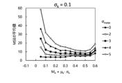
- FIG. 15B is a diagram showing the average MSE between the correct image and the restored image for five wavelength bands when random noise is superimposed on the compressed image.
- 19C shows that when optical filter f i receives light Iin from an object, optical filter f i outputs light Iout i , and when photodetector d i detects light Iout i , it outputs signal s i .
- all or part of a circuit, unit, device, member, or part, or all or part of a functional block in a block diagram may be implemented by one or more electronic circuits including, for example, a semiconductor device, a semiconductor integrated circuit (IC), or an LSI (large scale integration).
- the LSI or IC may be integrated into one chip, or may be configured by combining multiple chips.
- functional blocks other than memory elements may be integrated into one chip.
- LSI or IC are referred to as such, but the name may change depending on the degree of integration, and may be called a system LSI, VLSI (very large scale integration), or ULSI (ultra large scale integration).
- noises such as read noise, optical shot noise, and fixed pattern noise may be superimposed on the compressed image.
- the noise increases the restoration error when generating the restored image.
- the light detection device which can be used in a hyperspectral camera, can solve this problem.
- the light detection device includes N pixels, each of which includes an optical filter and a light detection element. By appropriately designing the optical filter and light detection element included in each pixel, the effect of noise on the restored image can be reduced.
- FIG. 1A is a diagram showing a schematic configuration example of a light detection system.
- the light detection system 300 shown in FIG. 1A includes a light detection device 100 and an image processing device 200.
- the light detection device 100 has a configuration similar to that of the light detection device disclosed in Patent Document 1.
- the light detection device 100 includes an optical system 140, a filter array 110, and an image sensor 160.
- the optical system 140 and the filter array 110 are disposed on the optical path of light incident from an object 70, which is a subject.
- the filter array 110 in the example of FIG. 1A is disposed between the optical system 140 and the image sensor 160.
- FIG. 1A illustrates an apple as an example of the object 70.
- the object 70 is not limited to an apple, and may be any object.
- the image sensor 160 generates data of a compressed image 10 in which information of a plurality of wavelength bands is compressed as a two-dimensional monochrome image.
- the image processing device 200 generates image data for each of a plurality of wavelength bands included in a predetermined target wavelength range based on the data of the compressed image 10 generated by the image sensor 160.
- the generated image data of the plurality of wavelength bands may be referred to as "hyperspectral image data".
- the number of wavelength bands included in the target wavelength range is M (M is an integer of 4 or more).
- the generated image data of the plurality of wavelength bands may be referred to as a restored image 20W 1 , a restored image 20W 2 , ..., a restored image 20W M , and these may be collectively referred to as a "hyperspectral image 20".
- a collection of data or signals representing an image i.e., data or signals representing the luminance value of each pixel, may also be simply referred to as an "image”.
- the filter array 110 is an array of multiple optical filters having translucency arranged in rows and columns.
- the optical filters are simply referred to as "filters.”
- the multiple filters include multiple types of filters with different spectral transmittances, i.e., wavelength dependence of transmittance.
- the types of filters may be, for example, three or four or more. In the case of four or more types, the types of filters may be, for example, four, nine, sixteen, or twenty-five.
- the filter array 110 modulates the intensity of the incident light for each wavelength and outputs it. This process by the filter array 110 is referred to as "encoding,” and the filter array 110 is also referred to as an "encoding element" or an "encoding mask.”
- the filter array 110 is disposed near or directly above the image sensor 160.
- “near” means close enough that a reasonably clear image of the light from the optical system 140 is formed on the surface of the filter array 110.
- “Directly above” means that the two are so close that there is almost no gap between them.
- the filter array 110 and the image sensor 160 may be integrated.
- FIGS. 1B to 1D are diagrams showing configuration examples of the light detection device 100 in which the filter array 110 is located away from the image sensor 160.
- the filter array 110 is located between the optical system 140 and the image sensor 160 and at a position away from the image sensor 160.
- the filter array 110 is located between the object 70 and the optical system 140.
- the light detection device 100 includes two optical systems 140A and 140B, and the filter array 110 is located between them.
- an optical system including one or more lenses may be located between the filter array 110 and the image sensor 160.
- the image sensor 160 is a monochrome type light detection device having a plurality of light detection elements arranged two-dimensionally.
- the image sensor 160 may be, for example, a charge-coupled device (CCD), a complementary metal oxide semiconductor (CMOS) sensor, or an infrared array sensor.
- the light detection elements include, for example, photodiodes.
- the image sensor 160 does not necessarily have to be a monochrome type sensor. For example, a sensor having a filter that transmits red light, a filter that transmits green light, and a filter that transmits blue light may be used. Alternatively, a sensor having a filter that transmits infrared light or white light in addition to these filters may be used.
- FIG. 2A is a diagram showing a schematic example of a filter array 110.
- the filter array 110 has multiple regions arranged two-dimensionally. In this specification, the regions are sometimes referred to as "cells.” Filters having individually set spectral transmittances are arranged in each region.
- the spectral transmittance is expressed as a function T( ⁇ ), where ⁇ is the wavelength of the incident light.
- the spectral transmittance T( ⁇ ) can take a value between 0 and 1.
- the filter array 110 has 48 rectangular regions arranged in 6 rows and 8 columns. This is merely an example, and in actual applications, more regions may be provided. The number may be approximately the same as the number of light detection elements in the image sensor 160, for example. The number of regions included in the filter array 110 is determined according to the application and may range from tens to tens of millions, for example.
- 2B is a diagram showing an example of the spatial distribution of the transmittance for each of the light in the wavelength bands W1 , W2 , ..., WM included in the target wavelength range.
- the difference in the shading of each region represents the difference in the transmittance. The lighter the region, the higher the transmittance, and the darker the region, the lower the transmittance.
- the spatial distribution of the transmittance differs depending on the wavelength band.
- 2C and 2D are diagrams showing examples of the spectral transmittance of the region A1 and the region A2 included in the filter array 110 shown in FIG. 2A, respectively.
- the spectral transmittance of the region A1 and the spectral transmittance of the region A2 are different from each other. In this way, the spectral transmittance of the filter array 110 varies depending on the region. However, it is not necessary that the spectral transmittance of all the regions is different.
- the spectral transmittance of at least some of the multiple regions is different from each other.
- the filter array 110 includes two or more filters having different spectral transmittances from each other.
- the number of patterns of the spectral transmittance of the multiple regions included in the filter array 110 may be equal to or greater than the number M of wavelength bands included in the target wavelength range.
- the filter array 110 may be designed so that the spectral transmittance of more than half of the regions is different.
- the target wavelength range W can be set to various ranges depending on the application.
- the target wavelength range W can be, for example, a visible light wavelength range of about 400 nm to about 700 nm, a near-infrared wavelength range of about 700 nm to about 2500 nm, or a near-ultraviolet wavelength range of about 10 nm to about 400 nm.
- the target wavelength range W may be a wavelength range such as mid-infrared or far-infrared. In this way, the wavelength range used is not limited to the visible light range.
- radiation in general, including infrared and ultraviolet rays, as well as visible light is referred to as "light”.
- M is an arbitrary integer equal to or greater than 4, and the wavelength bands obtained by dividing the target wavelength range W into M equal parts are wavelength band W 1 , wavelength band W 2 , ..., wavelength band W M.
- the multiple wavelength bands included in the target wavelength range W may be set arbitrarily.
- the bandwidth may be non-uniform depending on the wavelength band.
- the bandwidth differs depending on the wavelength band, and there is a gap between two adjacent wavelength bands. In this way, the method of determining the multiple wavelength bands is arbitrary.
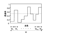
- FIG. 4A is a diagram for explaining the characteristics of the spectral transmittance in a certain region of the filter array 110.
- the spectral transmittance has multiple maximum values P1 to P5 and multiple minimum values with respect to wavelengths in the target wavelength range W.
- the maximum value of the transmittance in the target wavelength range W is normalized to 1 and the minimum value is 0.
- the spectral transmittance has maximum values in wavelength bands such as wavelength band W2 and wavelength band WM-1 . In this way, the spectral transmittance of each region can be designed to have maximum values in at least two wavelength ranges among the multiple wavelength bands included in the target wavelength range W.
- the maximum values P1, P3, P4, and P5 are 0.5 or more.
- FIG. 4B is a diagram showing an example of the spectral transmittance shown in FIG. 4A averaged for each wavelength band W 1 , W 2 , ..., W M.
- the averaged transmittance is obtained by integrating the spectral transmittance T( ⁇ ) for each wavelength band and dividing by the bandwidth of the wavelength band.
- the transmittance averaged for each wavelength band is defined as the transmittance for that wavelength band.
- the transmittance is remarkably high in the three wavelength ranges having the maximum value P1, the maximum value P3, and the maximum value P5.
- the transmittance exceeds 0.8 in the two wavelength ranges having the maximum value P3 and the maximum value P5.
- a grayscale transmittance distribution is assumed in which the transmittance of each region can take any value between 0 and 1 inclusive.
- a binary scale transmittance distribution may be adopted in which the transmittance of each region can take a value of either approximately 0 or approximately 1.
- each region transmits most of the light in at least two of the multiple wavelength ranges included in the target wavelength range, and does not transmit most of the light in the remaining wavelength ranges.
- "most" refers to approximately 80% or more.
- a part of all the cells may be replaced with a transparent region.
- a transparent region transmits light from all the wavelength bands W1 to WM included in the target wavelength range W with a similarly high transmittance, for example, a transmittance of 80% or more.
- the multiple transparent regions may be arranged, for example, in a checkerboard pattern. That is, in two arrangement directions of the multiple regions in the filter array 110, regions whose transmittance varies depending on the wavelength and transparent regions may be arranged alternately.
- the filter array 110 may be configured using, for example, a multilayer film, an organic material, a diffraction grating structure, a microstructure including a metal, or a metasurface.
- a dielectric multilayer film or a multilayer film including a metal layer may be used as the multilayer film.
- at least one of the thickness, material, and stacking order of each multilayer film is formed so that it differs for each cell. This allows different spectral characteristics to be realized for each cell.
- a multilayer film a sharp rise and fall in the spectral transmittance can be realized.
- a configuration using an organic material can be realized by making the pigment or dye contained different for each cell, or by stacking different materials.
- the photodetection device 100 has a plurality of light receiving regions with different optical response characteristics.
- the photodetection device 100 is equipped with a filter array 110 including a plurality of filters, and the plurality of filters have optical transmission characteristics that are irregularly different from one another
- the plurality of light receiving regions can be realized by an image sensor 160 arranged adjacent to or directly above the filter array 110.
- the optical response characteristics of the plurality of light receiving regions are determined based on the optical transmission characteristics of the plurality of filters included in the filter array 110.
- the data to be obtained is the data of the hyperspectral image 20, and the data is denoted as f.
- f is data obtained by integrating the image data f 1 , image data f 2 , ..., image data f M of each band.
- the horizontal direction of the image is the x direction
- the vertical direction of the image is the y direction.
- the number of pixels in the x direction of the image data to be obtained is m
- the number of pixels in the y direction is n
- each of the image data f 1 , image data f 2 , ..., image data f M is two-dimensional data of n x m pixels.
- the data f is three-dimensional data with the number of elements n x m x M.
- This three-dimensional data is called “hyperspectral image data” or “hyperspectral data cube”.
- the number of elements of the data g of the compressed image 10 obtained by encoding and multiplexing by the filter array 110 is n x m.
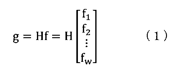
- the data g can be expressed by the following formula (1).
- the hyperspectral image 20 can be reconstructed by reflecting the influence of blurring of the encoding pattern by the PSF in the matrix H.
- the position at which the filter array 110 is placed is arbitrary, but a position can be selected that will not cause the coding pattern of the filter array 110 to become too diffuse and disappear.
- a hyperspectral image 20 can be restored from the compressed image 10 acquired by the filter array 110 and the image sensor 160. Details of the method for restoring the hyperspectral image 20 are disclosed in Patent Document 1. The disclosure of Patent Document 1 is incorporated herein by reference in its entirety.
- Example 1 of the photodetection device 100 capable of reducing the influence of noise In reality, when capturing an image of the object 70, noise may be superimposed on the compressed image 10. In the following, a first example of the light detection device 100 capable of reducing the influence of noise will be described.
- the photodetection device 100 can reduce the increase in restoration error due to noise even if noise is superimposed on the compressed image 10.
- noise that is independent of the amount of light was dealt with.
- the noise that is actually superimposed on the compressed image 10 includes not only read noise that is independent of the amount of light, but also, for example, optical shot noise that is proportional to the square root of the amount of light and fixed pattern noise that is proportional to the amount of light. Therefore, noise depends on the amount of light.
- the brightness value reflects the amount of light.
- FIG. 8 is a graph showing the relationship between the luminance value of each pixel in the compressed image 10 and the increase in restoration error in the corresponding pixel in the hyperspectral image 20 when the compressed image 10 is superimposed with actually measured noise.
- the object 70 is a white plate. When the target wavelength range is the visible range, the white plate reflects light in the target wavelength range with approximately the same reflectance regardless of the wavelength band. If the wavelength dependency of the reflectance is low, the object 70 does not need to be a white plate.
- the compressed image 10 was acquired under conditions where the average luminance value is 128.
- This condition which is least likely to cause blown-out highlights and blocked-up shadows and has a wide dynamic range, can be selected for general purposes.
- the compressed image 10 is acquired so that the average luminance value is the median value of the luminance range that can be acquired by the image sensor (128 in the case of 8-bit gradation).
- the ⁇ MSE is approximately 4%.
- the photodetection device 100 can be said to have N pixels.
- Each of the N pixels includes a filter and a photodetection element that detects light that has passed through the filter.
- the signal output from the photodetection element has information of four or more wavelength bands included in the target wavelength range superimposed thereon.
- T i ( ⁇ k )I( ⁇ k ) represents the wavelength dependency of the effective sensitivity of the i-th pixel.
- the wavelength dependency of the effective sensitivity of the i-th pixel may be T i ( ⁇ k )I i ( ⁇ k ).
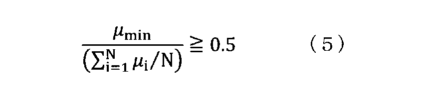
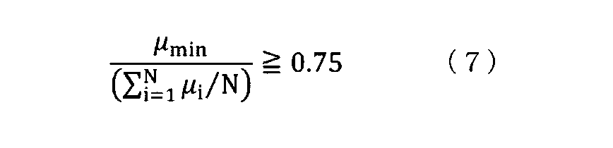
- ⁇ i corresponds to the luminance value of the i-th pixel in the compressed image 10 when the object 70 is a white board. Therefore, from the above discussion with reference to FIG. 8, if the minimum value among ⁇ 1 to ⁇ N is ⁇ min , then ⁇ MSE can be reduced to 10% or less when N pixels included in the light detection device 100 satisfy the following formula (5).
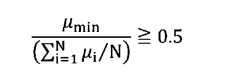
- the value 0.5 on the right side of formula (5) corresponds to the value obtained by dividing the lowest luminance value 64 by the average luminance value 128.
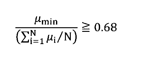
- the ⁇ MSE can be reduced to 7.5% or less.
- the value 0.68 on the right side of formula (6) corresponds to the value obtained by dividing the lowest luminance value, 87, by the average luminance value, 128.
- ⁇ i may be calculated based on T( ⁇ ) and I( ⁇ ). If the filter array 110 can be removed from the image sensor 160, T( ⁇ ) and I( ⁇ ) can be obtained separately. Even if it is not easy to remove the filter array 110 from the image sensor 160, I( ⁇ ) can be obtained from an image sensor of the same model number as the image sensor 160. Therefore, light of each of a plurality of wavelength bands included in the target wavelength range is detected using the filter array 110 and the image sensor 160, and T( ⁇ ) can be estimated based on T( ⁇ ) ⁇ I( ⁇ ) obtained from the detection result and the known I( ⁇ ).
- an object 70 having a triangular shape has both bright and dark parts.
- the filter array 110 shown in FIG. 10B has low transmittance in the part where the bright part of the object 70 is imaged, and has high transmittance in the part where the dark part of the object 70 is imaged.
- Step S104> The image processing device 220 generates a hyperspectral image 20 from the compressed image 10 with superimposed noise, using the above mask information stored in the storage device.
- a minimum value that the average value of the transmittance in the target wavelength range must satisfy is determined for the N filters included in the filter array 110 so that the increase in the restoration error is equal to or less than a predetermined value, as shown in Fig. 8.
- the predetermined value may be, for example, 10%, 7.5%, or 5%. In this manner, the transmission characteristics of the filter array 110 are determined.
- FIG. 13A is a diagram showing a schematic spatial pattern of the luminance values of the compressed image 10 for each of the light of a plurality of wavelength bands.
- the spatial pattern is expressed as a mosaic pattern.
- the distribution of the luminance values of the compressed image 10 differs depending on the wavelength band.
- M k ⁇ k - ⁇ k
- the filter array 110 includes multiple types of filters arranged irregularly.
- the photodetector 100 has noise resistance against random noise.
- M k does not need to be the same in all wavelength bands.
- M k may be the same in some wavelength bands, or may be different in all wavelength bands.
- the light detection device (Item 2) The light detection device according to the above item 1,
- the optical filter f i receives light Iin i from the object,
- the light Iin i includes light Iin i,W1 , ..., corresponding to the wavelength band W 1 , and light Iin i,WM corresponding to the wavelength band W M ,
- the optical filter f i receives a light Iin i
- the optical filter f i outputs a light Iout i ;
- the light Iout i includes light Iout i,W1 , . . .
- Light detection device That is, Light detection device.
- the transmission spectrum of the optical filter exhibits multiple peaks in the target wavelength range.
- the optical detection device according to any one of the first to third aspects.
- This light detection device can effectively encode the light from the target object.
- This light detection device can be used in hyperspectral cameras to reduce the effects of noise.
- This light detection device makes it easy to distinguish between filters, improving the accuracy of hyperspectral image restoration.
- noise resistance can be improved by increasing the transmittance.
- This photodetection device can reduce variation in the accuracy of restoring separated images across multiple wavelength bands.
- FIG. 9 A photodetector according to any one of techniques 1 to 8, A processing circuit; Equipped with the processing circuit generates four or more images corresponding to the four or more wavelength bands, respectively, based on image information obtained by signals output from the photodetection elements included in each of the N pixels and mask information indicating a spatial distribution of transmittance for each wavelength obtained from a transmission spectrum of the optical filter included in each of the N pixels.
- Optical detection system Optical detection system.
- This filter array can be used in hyperspectral cameras to reduce the effects of noise.
- This manufacturing method makes it possible to produce filter arrays that can be used in hyperspectral cameras and reduce the effects of noise.
Landscapes
- Physics & Mathematics (AREA)
- Spectroscopy & Molecular Physics (AREA)
- General Physics & Mathematics (AREA)
- Engineering & Computer Science (AREA)
- Multimedia (AREA)
- Signal Processing (AREA)
- Optics & Photonics (AREA)
- Transforming Light Signals Into Electric Signals (AREA)
- Investigating Or Analysing Materials By Optical Means (AREA)
- Spectrometry And Color Measurement (AREA)
- Solid State Image Pick-Up Elements (AREA)
Abstract
Description

以下では、まず、圧縮画像から復元画像を生成する光検出システムを説明する。次に、光検出システムに含まれる、ノイズの影響を低減できる光検出装置の例1および2を説明する。
図1Aは、光検出システムの構成例を模式的に示す図である。図1Aに示す光検出システム300は、光検出装置100と、画像処理装置200とを備える。光検出装置100は、特許文献1に開示された光検出装置と同様の構成を備える。光検出装置100は、光学系140と、フィルタアレイ110と、イメージセンサ160とを備える。光学系140およびフィルタアレイ110は、被写体である対象物70から入射する光の光路上に配置される。図1Aの例におけるフィルタアレイ110は、光学系140とイメージセンサ160との間に配置されている。

実際には、対象物70を撮像する際に、圧縮画像10にノイズが重畳され得る。以下では、ノイズの影響を低減できる光検出装置100の例1を説明する。
まず、図5を参照して、ノイズがハイパースペクトル画像20に及ぼす影響を説明する。図5は、ノイズが0%および2%である場合の、圧縮画像10と、ハイパースペクトル画像20の誤差マップとを示す図である。対象物70は蝶である。図5には、左上および左下に、それぞれ、0%および2%のノイズが重畳された圧縮画像10が示されている。図5には、さらに、右上および右下に、それぞれ、0%および2%のノイズが重畳された圧縮画像10から復元されたハイパースペクトル画像20の誤差マップが示されている。誤差マップは、対象波長域に含まれる複数の波長バンドについての復元画像と正解画像との間の復元誤差を平均化した値の空間分布に相当する。図5に示す誤差マップでは、白いほど誤差が大きく、黒いほど誤差が小さい。

次に、図6を参照して、ノイズによって復元誤差がどの程度増加するかを説明する。図6は、ノイズが2%である場合の、圧縮画像10内の各画素の輝度値と、ハイパースペクトル画像20内の対応する画素における復元誤差の増加量との関係を示すグラフである。ハイパースペクトル画像20内のある画素における復元誤差は、対象波長域に含まれる波長バンドについての復元画像内のある画素における復元誤差の平均値を意味する。圧縮画像10は、図5の左下の圧縮画像である。圧縮画像10は、2次元的に配列された512×512の画素を含む。輝度値は8ビット階調によって表され、輝度値の最小値は0であり、最大値は255である。各画素における復元誤差の増加量ΔMSEは、復元誤差MSE’から復元誤差MSE0を減算した値に相当する。復元誤差MSE’は、ノイズが重畳された圧縮画像10から復元されたハイパースペクトル画像20内の各画素における復元誤差である。復元誤差MSE0は、ノイズが重畳されていない圧縮画像10から復元されたハイパースペクトル画像20内の対応する画素における復元誤差である。図6に示す例において、復元誤差MSE’は図5の右下の誤差マップから得られ、復元誤差MSE0は図5の右上の誤差マップから得られる。図6に示すように、輝度値が小さくなるほど、ΔMSEが増加することがわかる。これは、輝度値が小さいほど、ノイズがハイパースペクトル画像20に及ぼす影響が大きくなることを意味する。
次に、図8を参照して、ノイズによる復元誤差の増加を低減する条件を説明する。図8は、圧縮画像10に実測したノイズを重畳した場合の、圧縮画像10内の各画素の輝度値と、ハイパースペクトル画像20内の対応する画素における復元誤差の増加量との関係を示すグラフである。対象物70は白板である。対象波長域が可視領域である場合、白板は、対象波長域内の光を、波長バンドに関係なく、ほぼ同じ反射率で反射する。反射率の波長依存性が低ければ、対象物70は白板である必要はない。圧縮画像10は、平均輝度値が128になる条件の下で取得された。白飛びおよび黒つぶれが最も生じにくく、広いダイナミックレンジが取れる当該条件は、汎用的に選択され得る。図8に関する以下の説明において、最低の輝度値および最高の輝度値がどのような値であるかに関係なく、圧縮画像10は、平均輝度値がイメージセンサの取得できる輝度範囲の中央値(8ビット階調である場合には128)になるように取得される。


次に、対象物70に対して汎用性のあるフィルタアレイ110を説明する。図10Aから図10Cは、それぞれ、対象物70、フィルタアレイ110、および圧縮画像10の例を模式的に示す図である。図10Aに示す色は、白いほど明るいことを意味し、黒いほど暗いことを意味する。図10Bに示す色は、白いほど透過率が高いことを意味し、黒いほど透過率が低いことを意味する。
次に、図12を参照して、フィルタアレイ110の製造方法を説明する。図12は、フィルタアレイ110の製造方法の例を概略的に示すフローチャートである。フィルタアレイ110の製造方法は、図12に示すステップS101~S107の工程を含む。フィルタアレイ110の製造方法は、例えば、工場の製造ラインにおいて機械によって実施され得る。あるいは、フィルタアレイ110の製造方法は、人によって実施されてもよい。
イメージセンサ160によって画像が複数のフレーム分取得される。フレーム数は、例えば、1000であり得る。
ステップS101において取得された複数のフレームにそれぞれ対応する複数の画像から、図7に示すように、輝度値に対するノイズの情報が取得される。
ステップS102において取得されたノイズが、記憶装置に記憶された上記の圧縮画像10に重畳される。
画像処理装置220により、ノイズが重畳された圧縮画像10から、記憶装置に記憶された上記のマスク情報を用いてハイパースペクトル画像20が生成される。
ステップS104において生成されたハイパースペクトル画像20と、記憶装置に記憶された上記のハイパースペクトル画像20とに基づいて、図8に示すように、輝度値と、復元誤差の増加量との関係が推定される。
ステップS106において推定された上記の関係に基づいて、図8に示すように、復元誤差の増加量が所定値以下になるように、フィルタアレイ110に含まれるN個のフィルタにおいて、透過率の対象波長域における平均値が満たすべき最低値が決定される。所定値は、例えば、10%、7.5%、または5%であり得る。このようにして、フィルタアレイ110の透過特性が決定される。
ステップS106において決定した透過特性に基づいて、フィルタアレイ110が製造される。
以下では、ノイズをランダムノイズに限定して、ノイズの影響を低減できる光検出装置100の例2を説明する。光検出装置100は、前述したN個の画素を備える。
ここでは、図13Aおよび図13Bを参照して、ランダムノイズの議論に用いられる、本実施形態による光検出装置100の特徴量を説明する。図13Aは、複数の波長バンドの各々の光についての圧縮画像10の輝度値の空間パターンを模式的に示す図である。当該空間パターンは、モザイクパターンとして表現されている。図13Aに示すように、波長バンドによって、圧縮画像10の輝度値の分布が異なる。図13Bは、対象波長域に含まれる4つ以上の波長バンドのうち、第k(kは1以上M以下の整数)の波長バンドの光についての圧縮画像10の輝度値から得られるヒストグラムの例を模式的に示す図である。第kの波長バンドの光は、第kの波長バンドに含まれる波長を有する光を意味する。図13Bに示す例において、横軸は輝度値を表し、縦軸はその輝度値を有する画素の数を表す。図13Bに示すヒストグラムから、特徴量として、第kの波長バンドの光についての圧縮画像10の輝度値の平均値μkおよび有限の標準偏差σkが得られる。第kの波長バンドの光がN個の画素の各々に入射する場合、μkは、N個の画素の各々に含まれる光検出素子から出力された信号の強度によって得られるN個の信号強度の平均値であり、σkは、当該N個の信号強度の標準偏差である。
次に、図14から図15Bを参照して、ランダムノイズが復元画像に及ぼす影響を説明する。図14は、ランダムノイズが重畳された圧縮画像10の例を模式的に示す図である。図14に示すように、ノイズ重畳後の圧縮画像は、ノイズ重畳前の圧縮画像と比較して不鮮明になり得る。

図13Bに示すμk-2σkの値が大きい光検出装置100は、高いノイズ耐性を有する。そのような光検出装置100では、輝度値が高いからである。図13Bに示すσkが大きい光検出装置100もまた、高いノイズ耐性を有する。そのような光検出装置100では、画素間の輝度値の分散が大きく画素同士の分別が容易であるため、復元画像の復元精度が向上するからである。以上のことから、μk-2σkおよびσkの和であるMk=μk-σkをノイズ耐性の指標として、本実施形態による光検出装置100を説明する。以下では、説明を簡単にするために、すべての波長バンドにおいてMk=μk-σkは同じであるものとする。本実施形態による光検出装置100において、フィルタアレイ110は、不規則に配列された複数種類のフィルタを含む。
・(Mkが小さい場合)波長バンド間のSN比は高い。したがって、σnoiseが小さいとき、復元画像の復元精度は高い。σnoiseが増加すると、フィルタアレイ110の少ない透過光量と比較して、ランダムノイズの量が無視できなくなる。その結果、復元誤差が増加し、復元画像の復元精度が大きく低下する。
・(Mkが大きすぎる場合)波長バンド間のSN比は低い。したがって、σnoiseが小さくても、復元画像の復元精度は低い。
・(Mkが適度に大きい場合)σnoiseが小さいとき、復元画像の復元精度は高い。σnoiseが増加しても、フィルタアレイ110の透過光量と比較して、ランダムノイズの量はそれほど大きくはならない。その結果、復元誤差の増加が低減され、復元画像の復元精度の低下が抑制される。
・複数の波長バンドの各々についてσk≧0.05である。この場合、画素同士の分別が容易であることから、復元画像の復元精度を向上させることができる。
・複数の波長バンドの各々についてμk≧0.2である。この場合、図16から図17Cに示す0.05≦σk≦0.1についてMk≧0.1が満たされる。
・複数の波長バンドについて最大のMkおよび最小のMkをそれぞれMmaxおよびMminとすると、Mmax/Mmin≦3である。この場合、複数の波長バンド間での復元画像の復元精度がばらつくことを抑制することができる。
ノイズの影響を低減できる本実施形態による光検出装置100の例1および2において、フィルタアレイ110は、複数のフィルタを含む。複数のフィルタのうち、少なくとも1つのフィルタの透過スペクトルは、対象波長域において複数のピークを示す。当該少なくとも1つのフィルタが共振構造を有する場合、複数のピークは共振構造に起因する。
本開示は上記した実施の形態に限定されるものではない。本開示の趣旨を逸脱しない限り、当業者が思いつく各種変形を上記実施の形態に施したものも本開示に含まれてもよい。本開示の実施の形態の変形例は下記に示すようなものであってもよい。
光学フィルタfiと、
前記光学フィルタfiから出力された被写体の第i情報を含む光を検出し、前記第i情報に対応する信号siを出力する光検出器diを含み、i=1、・・・、Nであり、Nは2以上の整数であり、
前記第i情報は、波長バンドW1に対応する前記被写体の情報Ii,1、~、波長バンドWMに対応する前記被写体の情報Ii,Mを含み(前記Mは4以上の整数)、
前記波長バンドW1、~、前記波長バンドWMは互いに異なり、

前記Ti,Wkは、前記光学フィルタfiの前記波長バンドWkの光透過率、
前記IWkは、前記光検出器d1、~、前記光検出器dNそれぞれの波長バンドWkに対応する光IWkの検出感度、
前記μminは、前記μ1、・・・、前記μNのうちの最小値であり、前記光学フィルタfiは前記光検出器diに直接接触し、または、前記光学フィルタfiと前記光検出器diの間にレンズとフィルタの両方が配置されることなく前記光学フィルタfiと前記光検出器diの距離はゼロより大きい、
光検出装置。
前記項目1に記載の光検出装置は、
前記光学フィルタfiは前記被写体からの光Iiniを受け取り、
前記光Iiniは、前記波長バンドW1に対応する光Iini,W1、~、前記波長バンドWMに対応する光Iini,WMを含み、
前記光学フィルタfiが光Iiniを受取ると、前記光学フィルタfiは光Ioutiを出力し、
前記光Ioutiは、前記波長バンドW1に対応する光Iouti,W1、~、前記波長バンドWMに対応する光Iouti,WMを含み、
前記透過率Ti,W1は(前記光Iouti,W1の強さ)/(前記Iini,W1の強さ)、~、前記透過率Ti,WMは(光Iouti,WMの強さ)/(光Iini,WMの強さ)
である。
図19Aは複数の光学フィルタと複数の光検出器の例を示す。光学フィルタf1は光検出器diに直接接触し、~、光学フィルタfiは光検出器diに直接接触し、~、光学フィルタfNは光検出器dNに直接接触する。
本開示において、「ハイパースペクトル画像を再構成する」は、「ハイパースペクトル画像を生成する」を意味してもよい。
以上の実施の形態の記載により、以下の技術が開示される。
N個の画素を備える光検出装置であって、
前記N個の画素の各々は、光学フィルタと、前記光学フィルタを透過した光を検出する光検出素子とを含み、
前記光検出素子から出力される信号には、対象波長域に含まれる4つ以上の波長バンドの情報が重畳されており、
前記N個の画素のうち、第iの画素(i=1、2、・・・、N)に含まれる前記光学フィルタの透過率の波長依存性と、前記第iの画素に含まれる前記光検出素子の検出感度の波長依存性とに基づく、前記第iの画素の実効感度の前記対象波長域における平均値をμiとし、μ1~μNのうち、最低値をμminとすると、

光検出装置。
技術1に記載の光検出装置。
前記N個の画素は、透過スペクトルが互いに異なる複数種類のフィルタを含み、前記複数種類のフィルタは不規則に配置され、
前記N個の画素のすべてにおいて、実効感度の前記対象波長域における平均値は同じである、
技術1または2に記載の光検出装置。
前記光学フィルタの透過スペクトルは、前記対象波長域において複数のピークを示す、
技術1から3のいずれかに記載の光検出装置。
N個の画素を備える光検出装置であって、
前記N個の画素の各々は、光学フィルタと、前記光学フィルタを透過した光を検出する光検出素子とを含み、
前記光検出素子から出力される信号には、対象波長域に含まれる4つ以上の波長バンドの情報が重畳されており、
前記4つ以上の波長バンドのうち、第kの波長バンド(k=1、2、・・・、N)の光が前記N個の画素の各々に入射した場合、前記N個の画素の各々に含まれる前記光検出素子から出力された信号の強度によって得られるN個の信号強度の平均値をμkとし、前記N個の信号強度の標準偏差をσkとし、Mk=μk―σkとすると、
前記4つ以上の波長バンドの各々について、Mk≧0.1である、
光検出装置。
前記N個の波長バンドの各々について、σk≧0.05である、
技術5に記載の光検出装置。
前記N個の波長バンドの各々について、μk≧0.2である、
技術5または6に記載の光検出装置。
前記N個の波長バンドについて、最大のMkをMmaxとし、最小のMkをMminとすると、
Mmax/Mmin≦3である、
技術5から7のいずれかに記載の光検出装置。
技術1から8のいずれかに記載の光検出装置と、
処理回路と、
を備え、
前記処理回路は、N個の画素の各々に含まれる前記光検出素子から出力された信号によって得られる画像情報と、N個の画素の各々に含まれる前記光学フィルタの透過スペクトルから得られる波長ごとの透過率の空間分布を示すマスク情報とに基づいて、前記4つ以上の波長バンドにそれぞれ対応する4つ以上の画像を生成する、
光検出システム。
対象波長域に含まれる4つ以上の波長バンドにそれぞれ対応する4つ以上の画像を生成する光検出装置に用いられるN個の光学フィルタを備えるフィルタアレイであって、
前記N個の光学フィルタのうち、第i画素(i=1、2、・・・、N)に含まれる光学フィルタの透過率の前記対象波長域における平均値をμiとし、μ1~μNのうち、最低値をμminとしたとき、
フィルタアレイ。
イメージセンサによって画像を複数のフレーム分取得する工程と、
前記複数のフレームにそれぞれ対応する複数の画像から、輝度値に対するノイズの情報を取得する工程と、
前記ノイズが重畳された圧縮画像から生成された復元画像と、前記ノイズが重畳される前の圧縮画像から生成された復元画像とに基づいて、輝度値と復元誤差の増加量との関係を推定する工程と、
推定した前記関係に基づいて、フィルタアレイの透過特性を決定する工程と、
決定した前記透過特性に基づいて、フィルタアレイを製造する工程と、
を含む、
フィルタアレイの製造方法。
20、20W1、20W2、・・・、20WN 復元画像
70 対象物
100 光検出装置
110 フィルタアレイ
112、114 フィルタ
140、140A、140B 光学系
160 イメージセンサ
200 画像処理装置
300 光検出システム
Claims (10)
- N個の画素を備える光検出装置であって、
前記N個の画素の各々は、光学フィルタと、前記光学フィルタを透過した光を検出する光検出素子とを含み、
前記光検出素子から出力される信号には、対象波長域に含まれる4つ以上の波長バンドの情報が重畳されており、
前記N個の画素のうち、第iの画素(i=1、2、・・・、N)に含まれる前記光学フィルタの透過率の波長依存性と、前記第iの画素に含まれる前記光検出素子の検出感度の波長依存性とに基づく、前記第iの画素の実効感度の前記対象波長域における平均値をμiとし、μ1~μNのうち、最低値をμminとすると、

光検出装置。 -

請求項1に記載の光検出装置。 - 前記N個の画素は、透過スペクトルが互いに異なる複数種類のフィルタを含み、前記複数種類のフィルタは不規則に配置され、
前記N個の画素のすべてにおいて、実効感度の前記対象波長域における平均値は同じである、
請求項1または2に記載の光検出装置。 - 前記光学フィルタの透過スペクトルは、前記対象波長域において複数のピークを示す、
請求項1または2に記載の光検出装置。 - N個の画素を備える光検出装置であって、
前記N個の画素の各々は、光学フィルタと、前記光学フィルタを透過した光を検出する光検出素子とを含み、
前記光検出素子から出力される信号には、対象波長域に含まれる4つ以上の波長バンドの情報が重畳されており、
前記4つ以上の波長バンドのうち、第kの波長バンド(k=1、2、・・・、N)の光が前記N個の画素の各々に入射した場合、前記N個の画素の各々に含まれる前記光検出素子から出力された信号の強度によって得られるN個の信号強度の平均値をμkとし、前記N個の信号強度の標準偏差をσkとし、Mk=μk-σkとすると、
前記4つ以上の波長バンドの各々について、Mk≧0.1である、
光検出装置。 - 前記N個の波長バンドの各々について、σk≧0.05である、
請求項5に記載の光検出装置。 - 前記N個の波長バンドの各々について、μk≧0.2である、
請求項5または6に記載の光検出装置。 - 前記N個の波長バンドについて、最大のMkをMmaxとし、最小のMkをMminとすると、
Mmax/Mmin≦3である、
請求項5または6に記載の光検出装置。 - 請求項1または5に記載の光検出装置と、
処理回路と、
を備え、
前記処理回路は、N個の画素の各々に含まれる前記光検出素子から出力された信号によって得られる画像情報と、N個の画素の各々に含まれる前記光学フィルタの透過スペクトルから得られる波長ごとの透過率の空間分布を示すマスク情報とに基づいて、前記4つ以上の波長バンドにそれぞれ対応する4つ以上の画像を生成する、
光検出システム。 - 対象波長域に含まれる4つ以上の波長バンドにそれぞれ対応する4つ以上の画像を生成する光検出装置に用いられるN個の光学フィルタを備えるフィルタアレイであって、
前記N個の光学フィルタのうち、第i画素(i=1、2、・・・、N)に含まれる光学フィルタの透過率の前記対象波長域における平均値をμiとし、μ1~μNのうち、最低値をμminとしたとき、

フィルタアレイ。
Priority Applications (4)
| Application Number | Priority Date | Filing Date | Title |
|---|---|---|---|
| CN202380083796.9A CN120344839A (zh) | 2022-12-27 | 2023-11-22 | 光检测装置、光检测系统及滤光器阵列 |
| JP2024567296A JPWO2024142683A1 (ja) | 2022-12-27 | 2023-11-22 | |
| EP23911465.5A EP4644850A4 (en) | 2022-12-27 | 2023-11-22 | OPTICAL DETECTION DEVICE, OPTICAL DETECTION SYSTEM AND FILTER MATRIX |
| US19/235,168 US20250305880A1 (en) | 2022-12-27 | 2025-06-11 | Light detection apparatus, light detection system, and filter array |
Applications Claiming Priority (2)
| Application Number | Priority Date | Filing Date | Title |
|---|---|---|---|
| JP2022209176 | 2022-12-27 | ||
| JP2022-209176 | 2022-12-27 |
Related Child Applications (1)
| Application Number | Title | Priority Date | Filing Date |
|---|---|---|---|
| US19/235,168 Continuation US20250305880A1 (en) | 2022-12-27 | 2025-06-11 | Light detection apparatus, light detection system, and filter array |
Publications (1)
| Publication Number | Publication Date |
|---|---|
| WO2024142683A1 true WO2024142683A1 (ja) | 2024-07-04 |
Family
ID=91717109
Family Applications (1)
| Application Number | Title | Priority Date | Filing Date |
|---|---|---|---|
| PCT/JP2023/041925 Ceased WO2024142683A1 (ja) | 2022-12-27 | 2023-11-22 | 光検出装置、光検出システム、およびフィルタアレイ |
Country Status (5)
| Country | Link |
|---|---|
| US (1) | US20250305880A1 (ja) |
| EP (1) | EP4644850A4 (ja) |
| JP (1) | JPWO2024142683A1 (ja) |
| CN (1) | CN120344839A (ja) |
| WO (1) | WO2024142683A1 (ja) |
Citations (4)
| Publication number | Priority date | Publication date | Assignee | Title |
|---|---|---|---|---|
| US9599511B2 (en) | 2014-11-19 | 2017-03-21 | Panasonic Intellectual Property Management Co., Ltd. | Imaging apparatus comprising coding element and spectroscopic system comprising the imaging apparatus |
| JP6952283B1 (ja) * | 2020-01-16 | 2021-10-20 | パナソニックIpマネジメント株式会社 | 光学フィルタアレイ、光検出装置、および光検出システム |
| US20210341657A1 (en) | 2019-03-06 | 2021-11-04 | Panasonic Intellectual Property Management Co., Ltd. | Photodetection device, photodetection system, and filter array |
| WO2021241171A1 (ja) | 2020-05-29 | 2021-12-02 | パナソニックIpマネジメント株式会社 | フィルタアレイおよび光検出システム |
Family Cites Families (4)
| Publication number | Priority date | Publication date | Assignee | Title |
|---|---|---|---|---|
| SE0402576D0 (sv) * | 2004-10-25 | 2004-10-25 | Forskarpatent I Uppsala Ab | Multispectral and hyperspectral imaging |
| EP3186604A1 (en) * | 2014-08-25 | 2017-07-05 | Montana State University | Microcavity array for spectral imaging |
| JP6478579B2 (ja) * | 2014-11-20 | 2019-03-06 | キヤノン株式会社 | 撮像ユニット、撮像装置、及び画像処理システム |
| EP3913341A4 (en) * | 2019-01-16 | 2022-02-23 | Panasonic Intellectual Property Management Co., Ltd. | OPTICAL FILTER, PHOTO DETECTION DEVICE AND PHOTO DETECTION SYSTEM |
-
2023
- 2023-11-22 EP EP23911465.5A patent/EP4644850A4/en active Pending
- 2023-11-22 JP JP2024567296A patent/JPWO2024142683A1/ja active Pending
- 2023-11-22 CN CN202380083796.9A patent/CN120344839A/zh active Pending
- 2023-11-22 WO PCT/JP2023/041925 patent/WO2024142683A1/ja not_active Ceased
-
2025
- 2025-06-11 US US19/235,168 patent/US20250305880A1/en active Pending
Patent Citations (5)
| Publication number | Priority date | Publication date | Assignee | Title |
|---|---|---|---|---|
| US9599511B2 (en) | 2014-11-19 | 2017-03-21 | Panasonic Intellectual Property Management Co., Ltd. | Imaging apparatus comprising coding element and spectroscopic system comprising the imaging apparatus |
| US20210341657A1 (en) | 2019-03-06 | 2021-11-04 | Panasonic Intellectual Property Management Co., Ltd. | Photodetection device, photodetection system, and filter array |
| JP6952283B1 (ja) * | 2020-01-16 | 2021-10-20 | パナソニックIpマネジメント株式会社 | 光学フィルタアレイ、光検出装置、および光検出システム |
| WO2021241171A1 (ja) | 2020-05-29 | 2021-12-02 | パナソニックIpマネジメント株式会社 | フィルタアレイおよび光検出システム |
| JP7142251B2 (ja) * | 2020-05-29 | 2022-09-27 | パナソニックIpマネジメント株式会社 | フィルタアレイおよび光検出システム |
Non-Patent Citations (1)
| Title |
|---|
| See also references of EP4644850A1 |
Also Published As
| Publication number | Publication date |
|---|---|
| CN120344839A (zh) | 2025-07-18 |
| EP4644850A1 (en) | 2025-11-05 |
| EP4644850A4 (en) | 2026-04-29 |
| JPWO2024142683A1 (ja) | 2024-07-04 |
| US20250305880A1 (en) | 2025-10-02 |
Similar Documents
| Publication | Publication Date | Title |
|---|---|---|
| JP7720532B2 (ja) | 信号処理方法、信号処理装置、および撮像システム | |
| Peng et al. | Learned large field-of-view imaging with thin-plate optics. | |
| JP7668452B2 (ja) | 信号処理方法、信号処理装置、および撮像システム | |
| US11843876B2 (en) | Optical filter array, photodetection device, and photodetection system | |
| JP7829156B2 (ja) | 画像処理装置、撮像システム、および復元画像の誤差を推定する方法 | |
| JP7142251B2 (ja) | フィルタアレイおよび光検出システム | |
| JP7756327B2 (ja) | 分光画像を生成する処理に用いられるデータを処理する方法および装置 | |
| JP7811739B2 (ja) | 検査対象に含まれる異物を検出する方法および装置 | |
| WO2023286613A1 (ja) | フィルタアレイ、光検出装置、および光検出システム | |
| WO2021241122A1 (ja) | フィルタアレイおよび光検出システム | |
| CN119654651A (zh) | 信号处理方法及信号处理装置 | |
| WO2024203282A1 (ja) | 撮像システムおよび方法 | |
| US20250305880A1 (en) | Light detection apparatus, light detection system, and filter array | |
| JP7122636B2 (ja) | フィルタアレイおよび光検出システム | |
| Schöberl et al. | Building a high dynamic range video sensor with spatially nonregular optical filtering | |
| WO2022168594A1 (ja) | スペクトルデータキューブを改変する方法および装置 | |
| WO2023106142A1 (ja) | 信号処理方法、プログラム、およびシステム | |
| JP2025071703A (ja) | 画像を生成するシステムに用いられる装置およびフィルタアレイ | |
| WO2024195499A1 (ja) | 撮像システム、行列データ、および行列データの生成方法 | |
| WO2023106143A1 (ja) | 分光画像を生成するシステムに用いられる装置およびフィルタアレイ、分光画像を生成するシステム、ならびにフィルタアレイの製造方法 | |
| WO2026088780A1 (ja) | 情報処理方法、処理装置、およびコンピュータプログラム | |
| WO2025192485A1 (ja) | 撮像システムおよび撮像方法 | |
| JP2024020922A (ja) | 復元画像の評価方法および撮像システム、 | |
| WO2025192316A1 (ja) | 撮像装置、撮像システム、および撮像方法 | |
| WO2025084081A1 (ja) | 撮像システムおよびそれに用いられる方法 |
Legal Events
| Date | Code | Title | Description |
|---|---|---|---|
| 121 | Ep: the epo has been informed by wipo that ep was designated in this application |
Ref document number: 23911465 Country of ref document: EP Kind code of ref document: A1 |
|
| WWE | Wipo information: entry into national phase |
Ref document number: 202380083796.9 Country of ref document: CN |
|
| WWE | Wipo information: entry into national phase |
Ref document number: 2024567296 Country of ref document: JP |
|
| WWP | Wipo information: published in national office |
Ref document number: 202380083796.9 Country of ref document: CN |
|
| WWE | Wipo information: entry into national phase |
Ref document number: 2023911465 Country of ref document: EP |
|
| NENP | Non-entry into the national phase |
Ref country code: DE |
|
| ENP | Entry into the national phase |
Ref document number: 2023911465 Country of ref document: EP Effective date: 20250728 |
|
| ENP | Entry into the national phase |
Ref document number: 2023911465 Country of ref document: EP Effective date: 20250728 |
|
| WWP | Wipo information: published in national office |
Ref document number: 2023911465 Country of ref document: EP |