WO2024142977A1 - コイルばねおよびその製造方法 - Google Patents
コイルばねおよびその製造方法 Download PDFInfo
- Publication number
- WO2024142977A1 WO2024142977A1 PCT/JP2023/044883 JP2023044883W WO2024142977A1 WO 2024142977 A1 WO2024142977 A1 WO 2024142977A1 JP 2023044883 W JP2023044883 W JP 2023044883W WO 2024142977 A1 WO2024142977 A1 WO 2024142977A1
- Authority
- WO
- WIPO (PCT)
- Prior art keywords
- layer
- wire
- hardness
- coil spring
- hardness distribution
- Prior art date
- Legal status (The legal status is an assumption and is not a legal conclusion. Google has not performed a legal analysis and makes no representation as to the accuracy of the status listed.)
- Ceased
Links
Images




Classifications
-
- B—PERFORMING OPERATIONS; TRANSPORTING
- B21—MECHANICAL METAL-WORKING WITHOUT ESSENTIALLY REMOVING MATERIAL; PUNCHING METAL
- B21F—WORKING OR PROCESSING OF METAL WIRE
- B21F35/00—Making springs from wire
-
- B—PERFORMING OPERATIONS; TRANSPORTING
- B21—MECHANICAL METAL-WORKING WITHOUT ESSENTIALLY REMOVING MATERIAL; PUNCHING METAL
- B21F—WORKING OR PROCESSING OF METAL WIRE
- B21F3/00—Coiling wire into particular forms
- B21F3/02—Coiling wire into particular forms helically
-
- C—CHEMISTRY; METALLURGY
- C21—METALLURGY OF IRON
- C21D—MODIFYING THE PHYSICAL STRUCTURE OF FERROUS METALS; GENERAL DEVICES FOR HEAT TREATMENT OF FERROUS OR NON-FERROUS METALS OR ALLOYS; MAKING METAL MALLEABLE, e.g. BY DECARBURISATION OR TEMPERING
- C21D1/00—General methods or devices for heat treatment, e.g. annealing, hardening, quenching or tempering
- C21D1/06—Surface hardening
-
- C—CHEMISTRY; METALLURGY
- C21—METALLURGY OF IRON
- C21D—MODIFYING THE PHYSICAL STRUCTURE OF FERROUS METALS; GENERAL DEVICES FOR HEAT TREATMENT OF FERROUS OR NON-FERROUS METALS OR ALLOYS; MAKING METAL MALLEABLE, e.g. BY DECARBURISATION OR TEMPERING
- C21D1/00—General methods or devices for heat treatment, e.g. annealing, hardening, quenching or tempering
- C21D1/18—Hardening; Quenching with or without subsequent tempering
-
- C—CHEMISTRY; METALLURGY
- C21—METALLURGY OF IRON
- C21D—MODIFYING THE PHYSICAL STRUCTURE OF FERROUS METALS; GENERAL DEVICES FOR HEAT TREATMENT OF FERROUS OR NON-FERROUS METALS OR ALLOYS; MAKING METAL MALLEABLE, e.g. BY DECARBURISATION OR TEMPERING
- C21D1/00—General methods or devices for heat treatment, e.g. annealing, hardening, quenching or tempering
- C21D1/18—Hardening; Quenching with or without subsequent tempering
- C21D1/25—Hardening, combined with annealing between 300 degrees Celsius and 600 degrees Celsius, i.e. heat refining ("Vergüten")
-
- C—CHEMISTRY; METALLURGY
- C21—METALLURGY OF IRON
- C21D—MODIFYING THE PHYSICAL STRUCTURE OF FERROUS METALS; GENERAL DEVICES FOR HEAT TREATMENT OF FERROUS OR NON-FERROUS METALS OR ALLOYS; MAKING METAL MALLEABLE, e.g. BY DECARBURISATION OR TEMPERING
- C21D1/00—General methods or devices for heat treatment, e.g. annealing, hardening, quenching or tempering
- C21D1/34—Methods of heating
- C21D1/40—Direct resistance heating
-
- C—CHEMISTRY; METALLURGY
- C21—METALLURGY OF IRON
- C21D—MODIFYING THE PHYSICAL STRUCTURE OF FERROUS METALS; GENERAL DEVICES FOR HEAT TREATMENT OF FERROUS OR NON-FERROUS METALS OR ALLOYS; MAKING METAL MALLEABLE, e.g. BY DECARBURISATION OR TEMPERING
- C21D7/00—Modifying the physical properties of iron or steel by deformation
- C21D7/02—Modifying the physical properties of iron or steel by deformation by cold working
- C21D7/04—Modifying the physical properties of iron or steel by deformation by cold working of the surface
- C21D7/06—Modifying the physical properties of iron or steel by deformation by cold working of the surface by shot-peening or the like
-
- C—CHEMISTRY; METALLURGY
- C21—METALLURGY OF IRON
- C21D—MODIFYING THE PHYSICAL STRUCTURE OF FERROUS METALS; GENERAL DEVICES FOR HEAT TREATMENT OF FERROUS OR NON-FERROUS METALS OR ALLOYS; MAKING METAL MALLEABLE, e.g. BY DECARBURISATION OR TEMPERING
- C21D7/00—Modifying the physical properties of iron or steel by deformation
- C21D7/13—Modifying the physical properties of iron or steel by deformation by hot working
-
- C—CHEMISTRY; METALLURGY
- C21—METALLURGY OF IRON
- C21D—MODIFYING THE PHYSICAL STRUCTURE OF FERROUS METALS; GENERAL DEVICES FOR HEAT TREATMENT OF FERROUS OR NON-FERROUS METALS OR ALLOYS; MAKING METAL MALLEABLE, e.g. BY DECARBURISATION OR TEMPERING
- C21D8/00—Modifying the physical properties of ferrous metals or ferrous alloys by deformation combined with, or followed by, heat treatment
- C21D8/06—Modifying the physical properties of ferrous metals or ferrous alloys by deformation combined with, or followed by, heat treatment during manufacturing of rods or wires
-
- C—CHEMISTRY; METALLURGY
- C21—METALLURGY OF IRON
- C21D—MODIFYING THE PHYSICAL STRUCTURE OF FERROUS METALS; GENERAL DEVICES FOR HEAT TREATMENT OF FERROUS OR NON-FERROUS METALS OR ALLOYS; MAKING METAL MALLEABLE, e.g. BY DECARBURISATION OR TEMPERING
- C21D9/00—Heat treatment, e.g. annealing, hardening, quenching or tempering, adapted for particular articles; Furnaces therefor
- C21D9/02—Heat treatment, e.g. annealing, hardening, quenching or tempering, adapted for particular articles; Furnaces therefor for springs
-
- C—CHEMISTRY; METALLURGY
- C21—METALLURGY OF IRON
- C21D—MODIFYING THE PHYSICAL STRUCTURE OF FERROUS METALS; GENERAL DEVICES FOR HEAT TREATMENT OF FERROUS OR NON-FERROUS METALS OR ALLOYS; MAKING METAL MALLEABLE, e.g. BY DECARBURISATION OR TEMPERING
- C21D9/00—Heat treatment, e.g. annealing, hardening, quenching or tempering, adapted for particular articles; Furnaces therefor
- C21D9/52—Heat treatment, e.g. annealing, hardening, quenching or tempering, adapted for particular articles; Furnaces therefor for wires; for strips ; for rods of unlimited length
- C21D9/525—Heat treatment, e.g. annealing, hardening, quenching or tempering, adapted for particular articles; Furnaces therefor for wires; for strips ; for rods of unlimited length for wire, for rods
-
- F—MECHANICAL ENGINEERING; LIGHTING; HEATING; WEAPONS; BLASTING
- F16—ENGINEERING ELEMENTS AND UNITS; GENERAL MEASURES FOR PRODUCING AND MAINTAINING EFFECTIVE FUNCTIONING OF MACHINES OR INSTALLATIONS; THERMAL INSULATION IN GENERAL
- F16F—SPRINGS; SHOCK-ABSORBERS; MEANS FOR DAMPING VIBRATION
- F16F1/00—Springs
- F16F1/02—Springs made of steel or other material having low internal friction; Wound, torsion, leaf, cup, ring or the like springs, the material of the spring not being relevant
- F16F1/024—Covers or coatings therefor
-
- F—MECHANICAL ENGINEERING; LIGHTING; HEATING; WEAPONS; BLASTING
- F16—ENGINEERING ELEMENTS AND UNITS; GENERAL MEASURES FOR PRODUCING AND MAINTAINING EFFECTIVE FUNCTIONING OF MACHINES OR INSTALLATIONS; THERMAL INSULATION IN GENERAL
- F16F—SPRINGS; SHOCK-ABSORBERS; MEANS FOR DAMPING VIBRATION
- F16F1/00—Springs
- F16F1/02—Springs made of steel or other material having low internal friction; Wound, torsion, leaf, cup, ring or the like springs, the material of the spring not being relevant
- F16F1/04—Wound springs
- F16F1/06—Wound springs with turns lying in cylindrical surfaces
-
- F—MECHANICAL ENGINEERING; LIGHTING; HEATING; WEAPONS; BLASTING
- F16—ENGINEERING ELEMENTS AND UNITS; GENERAL MEASURES FOR PRODUCING AND MAINTAINING EFFECTIVE FUNCTIONING OF MACHINES OR INSTALLATIONS; THERMAL INSULATION IN GENERAL
- F16F—SPRINGS; SHOCK-ABSORBERS; MEANS FOR DAMPING VIBRATION
- F16F2226/00—Manufacturing; Treatments
- F16F2226/02—Surface treatments
-
- F—MECHANICAL ENGINEERING; LIGHTING; HEATING; WEAPONS; BLASTING
- F16—ENGINEERING ELEMENTS AND UNITS; GENERAL MEASURES FOR PRODUCING AND MAINTAINING EFFECTIVE FUNCTIONING OF MACHINES OR INSTALLATIONS; THERMAL INSULATION IN GENERAL
- F16F—SPRINGS; SHOCK-ABSORBERS; MEANS FOR DAMPING VIBRATION
- F16F2226/00—Manufacturing; Treatments
- F16F2226/04—Assembly or fixing methods; methods to form or fashion parts
-
- F—MECHANICAL ENGINEERING; LIGHTING; HEATING; WEAPONS; BLASTING
- F16—ENGINEERING ELEMENTS AND UNITS; GENERAL MEASURES FOR PRODUCING AND MAINTAINING EFFECTIVE FUNCTIONING OF MACHINES OR INSTALLATIONS; THERMAL INSULATION IN GENERAL
- F16F—SPRINGS; SHOCK-ABSORBERS; MEANS FOR DAMPING VIBRATION
- F16F2238/00—Type of springs or dampers
- F16F2238/02—Springs
- F16F2238/026—Springs wound- or coil-like
Definitions
- the wire may have a first layer and a second layer inside the first layer, and the hardness of the first layer may be less than the hardness of the second layer.
- the first hardness distribution and the second hardness distribution may be different.
- the difference between the first hardness distribution and the second hardness distribution is caused by a difference in at least one of the width of the first layer, the width of the second layer, and the minimum value of the hardness in the first layer.
- the method of manufacturing a coil spring includes forming the wire into a spiral shape, attaching a first terminal and a second terminal connected to a power source capable of supplying alternating current to the wire, and passing an alternating current through the wire via the first terminal and the second terminal to heat the wire, thereby forming a hardness distribution that varies in the circumferential direction in at least a portion of the wire.
- the manufacturing method may further include, before passing the AC current through the strand, placing an electrically floating conductor in a position that will cause a proximity effect when the AC current is passed through the strand.
- the manufacturing method may further include subjecting the wire formed into a spiral shape to shot peening to impart compressive residual stress to the wire.
- the present invention provides a coil spring with improved circumferential characteristics of the wire and a method for manufacturing the same.
- FIG. 8 is a flowchart showing an example of a method for manufacturing a coil spring.
- FIG. 9 is a diagram showing a schematic configuration of an AC current heating device that can be used in surface hardening.
- FIG. 10 is a schematic side view of the strands, conductors and ferromagnetic bodies assembled as shown in FIG.
- FIG. 11 is a schematic diagram for explaining the proximity effect.
- FIG. 12 is a graph showing another example of the hardness distribution that can be imparted to the wire.
- FIG. 1 is a schematic perspective view of a coil spring 1 according to this embodiment.
- the coil spring 1 has a wire 2 wound in a spiral shape around a coil axis X1.
- the wire 2 is made of spring steel, and its surface 20 is entirely covered with a coating 21.
- an axial direction DX parallel to the coil axis X1 and a radial direction DR centered on the coil axis X1 are defined.
- the coil spring 1 has an effective portion 10, a first winding seat portion 11, and a second winding seat portion 12.
- the effective portion 10 is located between the first winding seat portion 11 and the second winding seat portion 12.
- the first winding seat portion 11 is in a range of about one turn from the first terminal 2a of the wire 2
- the second winding seat portion 12 is in a range of about one turn from the second terminal 2b of the wire 2.
- the wire 2 is wound multiple times.
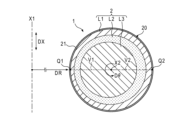
- FIG. 2 is a schematic cross-sectional view showing an example of a structure that can be applied to the coil spring 1.
- This cross-section corresponds to a transverse section perpendicular to the axis X2 of the wire 2.
- a circumferential direction D ⁇ is defined with the axis X2 as the center.
- at least a portion of the wire 2 has a hardness distribution that changes in the circumferential direction D ⁇ .
- the wire 2 has a first layer L1, a second layer L2 on the inside of the first layer L1, and a third layer L3 on the inside of the second layer L2.
- the hardness of the second layer L2 is smaller than the hardness of the first layer L1 and the third layer L3.
- the hardness of the second layer L2 has a gradient in the radial direction DR, as will be described later with reference to FIG. 3 etc.
- the above-mentioned surface 20 corresponds to the outer surface of the first layer L1.
- the first layer L1 and the second layer L2 are, for example, annular as shown in the figure, but are not limited to this example. In other words, the first layer L1 and the second layer L2 may be provided in a portion of the circumferential direction D ⁇ .
- the surface 20 of the wire 2 is, for example, a perfect circle centered on the axis X2.
- the boundary between the first layer L1 and the second layer L2, and the boundary between the second layer L2 and the third layer L3 are elliptical, the centers of which are offset from the axis X2.
- these boundaries may be perfect circles offset from the axis X2.
- the hard first layer L1 and third layer L3 ensure the settling resistance of the coil spring 1. Furthermore, the soft second layer L2 reduces the risk of breakage and also increases the corrosion fatigue resistance of the coil spring 1.
- the hardness distribution changes in the circumferential direction D ⁇ in at least a portion of the inside of the wire 2.
- a first line segment V1 and a second line segment V2 shown in FIG. 2 are defined.
- the first line segment V1 is a straight line connecting the first position Q1, which is located on the inner diameter side of the wire 2 on the surface 20, to the axis X2.
- the second line segment V2 is a straight line connecting the second position Q2, which is located on the outer diameter side of the wire 2 on the surface 20, to the axis X2.
- the first position Q1 is the part of the surface 20 that is closest to the coil axis X1.
- the second position Q2 is the part of the surface 20 that is farthest from the coil axis X1.
- the first position Q1, the axis X2, and the second position Q2 are aligned in the radial direction DR.
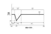
- FIG. 3 is a graph showing an example of a first hardness distribution H1 along a first line segment V1.
- FIG. 4 is a graph showing an example of a second hardness distribution H2 along a second line segment V2.
- the vertical axis is hardness (e.g., Vickers hardness HV)
- the horizontal axis is depth from the surface 20 of the wire 2 (distance from the surface 20).
- the width of the first layer L1 in the first hardness distribution H1 is defined as a1, the width of the second layer L2 as b1, the width of the third layer L3 as c1, the minimum value of hardness in the second layer L2 as d1, and the depth from the surface 20 (first position Q1) of the position of the minimum value as e1.
- the first hardness distribution H1 and the second hardness distribution H2 are different.
- such a difference between the hardness distributions H1 and H2 occurs because at least one of the widths a1 and a2, widths b1 and b2, widths c1 and c2, minimum values d1 and d2, and depths e1 and e2 is different.
- width a1 is smaller than width a2 (a1 ⁇ a2)
- width b1 is smaller than width b2 (b1 ⁇ b2)
- width c1 is larger than width c2 (c1>c2).
- depth e1 is smaller than depth e2 (e1 ⁇ e2).
- Minimum values d1 and d2 are, for example, equal, but may be different.
- the hardness distribution inside the wire 2 varies depending on the position in the circumferential direction D ⁇ .
- the hardness distribution of the wire 2 can be determined, for example, taking into consideration other characteristics required for each part in the circumferential direction D ⁇ .
- One example of the other characteristics is compressive residual stress imparted to the wire 2 by shot peening or the like.
- An example of the relationship between the residual stress distribution and hardness distribution of the wire 2 is described below.
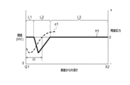
- FIG. 5 is a graph showing an example of a first hardness distribution H1 and a first residual stress distribution ⁇ 1 along the first line segment V1.
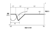
- FIG. 6 is a graph showing an example of a second hardness distribution H2 and a second residual stress distribution ⁇ 2 along the second line segment V2.
- the left vertical axis is hardness
- the right vertical axis is residual stress
- the horizontal axis is depth from the surface 20 of the wire 2.
- the position where the residual stress is zero coincides with the hardness of the first layer L1 and the third layer L3.
- the hardness distributions H1 and H2 shown in FIGS. 5 and 6 are similar to those shown in FIGS. 3 and 4.
- the shot material when shot peening is performed on a spirally wound wire 2, the shot material is likely to strike the outer diameter portion of the surface 20, but is unlikely to strike the inner diameter portion of the surface 20 or the portion located between adjacent wires 2 in the axial direction DX.
- compressive residual stress is imparted to a deep position in the outer diameter portion, but compressive residual stress is only imparted to a shallow position in the inner diameter portion, etc.
- the compressive residual stress imparted by shot peening can be non-uniform in the circumferential direction D ⁇ .
- compressive residual stress is imparted from the surface 20 (first position Q1) to the first range f1.
- compressive residual stress is imparted from the surface 20 (second position Q2) to the second range f2.
- the second range f2 extends to a deeper position than the first range f1.
- the first range f1 to which compressive residual stress is imparted overlaps the entire first layer L1 and extends into part of the second layer L2.
- the first range f1 does not extend into the third layer L3.
- the first range f1 may extend into part of the third layer L3.
- the peak of the compressive residual stress in the first range f1 is located closer to the surface 20 (first position Q1) than the position where the hardness is at a minimum in the first hardness distribution H1.
- the second range f2 to which compressive residual stress is imparted overlaps the entire first layer L1 and extends into part of the second layer L2.
- the second range f2 does not extend into the third layer L3.
- the second range f2 may extend into part of the third layer L3.
- the peak of the compressive residual stress in the second range f2 is located closer to the surface 20 (towards the second position Q2) than the position where the hardness is at a minimum in the second hardness distribution H2.
- hardness distributions H1, H2 are formed according to the residual stress distributions ⁇ 1, ⁇ 2.
- the second range f2 of the compressive residual stress extends to a position deeper than the first range f1, and the portion of the second layer L2 along the second line segment V2 is formed at a position deeper from the surface 20 than the portion of the second layer L2 along the first line segment V1. This results in substantially the same overlap between the first range f1 and the second layer L2, and between the second range f2 and the second layer L2.
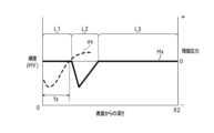
- FIG. 7 is a graph showing the hardness distribution Hx and residual stress distribution ⁇ x for the comparative example.
- compressive residual stress is imparted from the surface 20 to the range fx.
- the range fx overlaps with the first layer L1, but does not overlap with the second layer L2 or the third layer L3.
- the risk of breakage due to inclusions is reduced in areas where compressive residual stress is applied and areas where hardness is reduced.
- an area with low compressive residual stress and high hardness is generated near the boundary between the first layer L1 and the second layer L2. In this area, the risk of breakage due to inclusions increases.
- the relationship between hardness distribution Hx and residual stress distribution ⁇ x as shown in the comparative example in Figure 7 can arise, for example, when a uniform hardness distribution is imparted to wire 2 in the circumferential direction D ⁇ .
- the range in which compressive residual stress is imparted by shot peening is shallow on the inner diameter side and deep on the outer diameter side as described above, but if the hardness distribution in wire 2 is uniform in the circumferential direction D ⁇ , there is a possibility that the range in which hardness is reduced at any position in the circumferential direction D ⁇ and the range in which compressive residual stress is imparted will not overlap favorably.
- the width of the second layer L2 is increased at each position in the circumferential direction D ⁇ , the area with low compressive residual stress will overlap with the area with low hardness. However, if the proportion of the soft second layer L2 is increased in this way, the settling resistance of the coil spring 1 may decrease.
- the hardness distribution and residual stress distribution described using Figures 2 to 6 can be applied to any of the effective portion 10, the first winding portion 11, and the second winding portion 12.
- the hardness distribution and residual stress distribution in the effective portion 10, the first winding portion 11, and the second winding portion 12 may be substantially the same or different from each other.
- the second layer L2 may be provided on a portion of the wire 2 in the longitudinal direction along the axis X2.
- the wire 2 may be formed of two layers, a hard layer in the center and a soft layer around it, or may be formed of four or more layers in which adjacent layers have different hardnesses.
- the hardness distribution of the wire 2 in the circumferential direction D ⁇ does not necessarily need to be adjusted according to the compressive residual stress, but may be adjusted according to other characteristics of the wire 2, such as its structure.
- the hardness distribution of the wire 2 as illustrated in Figures 3 to 6 does not necessarily have to be different at all positions in the circumferential direction D ⁇ .
- the hardness distribution along the third line segment may be the same as either the first hardness distribution H1 or the second hardness distribution H2.
- FIG. 8 is a flow chart showing an example of a method for manufacturing the coil spring 1. This example corresponds to so-called hot forming, in which the straight wire 2 is first heated (step P1). Furthermore, the wire 2, which has become hot due to heating in step P1, is formed into a spiral shape by a coiling machine (step P2). In these steps P1 and P2, the wire 2 is quenched.
- step P2 surface hardening is performed to reduce the hardness of the inside of the wire 2 near the surface 20 (step P3).
- step P3 a second layer L2 with reduced hardness is formed as shown in Figures 3 to 6. Then, the wire 2 is tempered (step P4).
- step P4 the wire 2 is heated and subjected to hot setting, which applies an overload to the wire 2 (step P5). Furthermore, the wire 2 is subjected to shot peening (step P6). In this shot peening, compressive residual stresses such as those shown in Figures 5 and 6 are imparted to the wire 2.
- the wire 2 is pre-set (process P7). Furthermore, a coating film 21 is formed over the entire wire 2 (process P8). The coil spring 1 is completed at process P8.
- the conductor 3 is, for example, cylindrical and made of a metal material with excellent conductivity, such as copper or aluminum.
- the conductor 3 may have a laminated structure of a conductive layer made of a metal material and an insulating layer made of a resin or the like.
- the control device 5 is equipped with a power supply 51 that supplies alternating current.
- the first terminal 4A and the second terminal 4B are connected to the power supply 51 via wiring.
- the frequency of the alternating current supplied by the power supply 51 is not particularly limited, but as an example, a high frequency of 1 kHz or more may be used.
- the first terminal 4A and the second terminal 4B are each divided into a lower portion 41 and an upper portion 42.
- the first terminal 4A and the second terminal 4B can be attached to the wire 2 by sandwiching a part of the wire 2 between the lower portion 41 and the upper portion 42.
- the structure for attaching the first terminal 4A and the second terminal 4B to the wire 2 is not limited to this example.
- the first terminal 4A and the second terminal 4B are attached to the strand 2 formed into a spiral shape, and the strand 2 is placed inside the conductor 3. Note that there is no particular restriction on the order in which the process of attaching the first terminal 4A and the second terminal 4B to the strand 2 and the process of placing the strand 2 inside the conductor 3 are performed.
- the vicinity of the first terminal 2a and the second terminal 2b of the wire 2 protrudes from both ends of the conductor 3.
- This example is not limited, and the entire wire 2 may be surrounded by the conductor 3.
- the frequency, amplitude and duration of the alternating current can be determined appropriately depending on the shape of the wire 2 (e.g., wire diameter, cross-sectional shape, coil diameter, pitch, number of turns, coil length, material), the part to be heated and the target heating temperature.
- the control device 5 stops the current supply from the power source 51.
- a gap G1 is formed between the conductor 3 and the wire 2. That is, the inner surface of the conductor 3 faces the outer diameter side portion of the surface 20 of the wire 2 (the portion including the second position Q2 described above) via the gap G1.
- a gap G2 is formed between the ferromagnetic body 7 and the wire 2. That is, the outer surface of the ferromagnetic body 7 faces the inner diameter side portion of the surface 20 of the wire 2 (the portion including the first position Q1 described above) via the gap G2.
- the conductor 3s is positioned so that it faces only a portion of the workpiece Ws in the longitudinal direction of the workpiece Ws, it is possible to obtain a current density distribution and a heating temperature distribution that change depending on the longitudinal position on the surface and inside of the workpiece Ws.
- the current density distribution and heating temperature distribution can also be controlled by the material of the ferromagnetic body 7 and the gap G2 between the wire 2 and the ferromagnetic body 7.
- the ferromagnetic body 7 has the function of influencing the magnetic flux generated when a current is passed through the wire 2, spreading the current density toward the outer diameter.
- Fig. 12 is a graph showing another example of a hardness distribution that can be imparted to the wire 2.
- the hardness is low near the surface 20, and increases smoothly as it approaches the axis X2.
- the wire 2 has a first layer L1 and a second layer L2 inside it, and the hardness of the first layer L1 is smaller than the hardness of the second layer L2.
- the hardness distribution in the circumferential direction D ⁇ may change as in the examples described using FIG. 2 to FIG. 6.
- 1...coil spring 2...wire, X1...coil axis, X2...wire axis, DX...axial direction, DR...radial direction, D ⁇ ...circumferential direction, L1...first layer, L2...second layer, L3...third layer, H1...first hardness distribution, H2...second hardness distribution, ⁇ 1...first residual stress distribution, ⁇ 2...second residual stress distribution, 100...heating device.
Landscapes
- Engineering & Computer Science (AREA)
- Chemical & Material Sciences (AREA)
- Mechanical Engineering (AREA)
- Crystallography & Structural Chemistry (AREA)
- Materials Engineering (AREA)
- Metallurgy (AREA)
- Organic Chemistry (AREA)
- Physics & Mathematics (AREA)
- Thermal Sciences (AREA)
- General Engineering & Computer Science (AREA)
- Manufacturing & Machinery (AREA)
- Wire Processing (AREA)
Abstract
Description
Claims (12)
- 螺旋状に巻かれた素線により形成されるコイルばねであって、
前記素線の少なくとも一部は、前記素線の軸を中心とした周方向に変化する硬度分布を有している、
コイルばね。 - 前記素線は、第1層と、前記第1層の内側の第2層と、前記第2層の内側の第3層とを有し、
前記第2層の硬度は、前記第1層および前記第3層の硬度よりも小さい、
請求項1に記載のコイルばね。 - 前記素線の表面は、第1位置と、前記周方向において前記第1位置と離間した第2位置とを含み、
前記第1位置と前記軸を繋ぐ第1線分に沿う第1硬度分布と、前記第2位置と前記軸を繋ぐ第2線分に沿う第2硬度分布とが異なる、
請求項2に記載のコイルばね。 - 前記第1硬度分布および前記第2硬度分布において、前記第1層の幅、前記第2層の幅、前記第3層の幅、前記第2層における硬度の最小値、および、当該最小値の位置の前記表面からの深さの少なくとも一つが異なる、
請求項3に記載のコイルばね。 - 前記第1線分に沿う第1範囲および前記第2線分に沿う第2範囲のそれぞれに圧縮残留応力が付与されており、
前記第2範囲は、前記第1範囲よりも前記表面から深い位置に及び、
前記第2層のうち前記第2線分に沿う部分は、前記第2層のうち前記第1線分に沿う部分よりも前記表面から深い位置に形成されている、
請求項3に記載のコイルばね。 - 前記第1位置は、前記素線の内径側に位置し、
前記第2位置は、前記素線の外径側に位置する、
請求項5に記載のコイルばね。 - 前記素線は、第1層と、前記第1層の内側の第2層とを有し、
前記第1層の硬度は、前記第2層の硬度よりも小さい、
請求項1に記載のコイルばね。 - 前記素線の表面は、第1位置と、前記周方向において前記第1位置と離間した第2位置とを含み、
前記第1位置と前記軸を繋ぐ第1線分に沿う第1硬度分布と、前記第2位置と前記軸を繋ぐ第2線分に沿う第2硬度分布とが異なる、
請求項7に記載のコイルばね。 - 前記第1硬度分布および前記第2硬度分布において、前記第1層の幅、前記第2層の幅、および、前記第1層における硬度の最小値の少なくとも一つが異なる、
請求項8に記載のコイルばね。 - 請求項1乃至9のうちいずれか1項に記載のコイルばねの製造方法であって、
前記素線を螺旋状に成形し、
交流電流を供給可能な電源に接続された第1端子および第2端子を前記素線に取り付け、
前記第1端子および前記第2端子を通じて前記素線に交流電流を流して前記素線を加熱することにより、前記素線の少なくとも一部に前記周方向に変化する硬度分布を形成する、
ことを含むコイルばねの製造方法。 - 前記素線に前記交流電流を流す前に、電気的にフローティング状態である導体を前記素線への前記交流電流の通電時に近接効果を生じる位置に配置することをさらに含む、
請求項10に記載のコイルばねの製造方法。 - 螺旋状に成形された前記素線にショットピーニングを施して前記素線に圧縮残留応力を付与することをさらに含む、
請求項10に記載のコイルばねの製造方法。
Priority Applications (5)
| Application Number | Priority Date | Filing Date | Title |
|---|---|---|---|
| EP23911758.3A EP4644723A4 (en) | 2022-12-27 | 2023-12-14 | Helical spring and method of manufacturing the latter |
| MX2025007039A MX2025007039A (es) | 2022-12-27 | 2023-12-14 | Resorte helicoidal y metodo para su fabricacion |
| JP2024567477A JPWO2024142977A1 (ja) | 2022-12-27 | 2023-12-14 | |
| CN202380086461.2A CN120359364A (zh) | 2022-12-27 | 2023-12-14 | 螺旋弹簧及其制造方法 |
| US19/250,563 US20250320902A1 (en) | 2022-12-27 | 2025-06-26 | Coil spring and manufacturing method of the same |
Applications Claiming Priority (2)
| Application Number | Priority Date | Filing Date | Title |
|---|---|---|---|
| JP2022-210049 | 2022-12-27 | ||
| JP2022210049 | 2022-12-27 |
Related Child Applications (1)
| Application Number | Title | Priority Date | Filing Date |
|---|---|---|---|
| US19/250,563 Continuation US20250320902A1 (en) | 2022-12-27 | 2025-06-26 | Coil spring and manufacturing method of the same |
Publications (1)
| Publication Number | Publication Date |
|---|---|
| WO2024142977A1 true WO2024142977A1 (ja) | 2024-07-04 |
Family
ID=91717340
Family Applications (1)
| Application Number | Title | Priority Date | Filing Date |
|---|---|---|---|
| PCT/JP2023/044883 Ceased WO2024142977A1 (ja) | 2022-12-27 | 2023-12-14 | コイルばねおよびその製造方法 |
Country Status (6)
| Country | Link |
|---|---|
| US (1) | US20250320902A1 (ja) |
| EP (1) | EP4644723A4 (ja) |
| JP (1) | JPWO2024142977A1 (ja) |
| CN (1) | CN120359364A (ja) |
| MX (1) | MX2025007039A (ja) |
| WO (1) | WO2024142977A1 (ja) |
Citations (3)
| Publication number | Priority date | Publication date | Assignee | Title |
|---|---|---|---|---|
| JP2010133558A (ja) * | 2008-11-21 | 2010-06-17 | Muhr & Bender Kg | 硬化されたばね鋼、ばねエレメント及びばねエレメントを製造する方法 |
| JP6053916B2 (ja) | 2013-03-12 | 2016-12-27 | 本田技研工業株式会社 | ばね用鋼線およびその製造方法 |
| WO2018163541A1 (ja) * | 2017-03-10 | 2018-09-13 | 住友電気工業株式会社 | 斜め巻きばね用線材および斜め巻きばね |
Family Cites Families (3)
| Publication number | Priority date | Publication date | Assignee | Title |
|---|---|---|---|---|
| DE102004037721A1 (de) * | 2004-08-04 | 2006-02-23 | Robert Bosch Gmbh | Druckfeder zum Ansteuern eines dynamisch beanspruchten Elements |
| CN107387620A (zh) * | 2017-06-29 | 2017-11-24 | 太仓市惠得利弹簧有限公司 | 一种长寿命螺旋弹簧 |
| DE112018007004T5 (de) * | 2018-02-01 | 2020-10-29 | Sumitomo Electric Industries, Ltd. | Kupferbeschichteter Stahldraht und geneigte Spiralfeder |
-
2023
- 2023-12-14 EP EP23911758.3A patent/EP4644723A4/en active Pending
- 2023-12-14 MX MX2025007039A patent/MX2025007039A/es unknown
- 2023-12-14 CN CN202380086461.2A patent/CN120359364A/zh active Pending
- 2023-12-14 JP JP2024567477A patent/JPWO2024142977A1/ja active Pending
- 2023-12-14 WO PCT/JP2023/044883 patent/WO2024142977A1/ja not_active Ceased
-
2025
- 2025-06-26 US US19/250,563 patent/US20250320902A1/en active Pending
Patent Citations (3)
| Publication number | Priority date | Publication date | Assignee | Title |
|---|---|---|---|---|
| JP2010133558A (ja) * | 2008-11-21 | 2010-06-17 | Muhr & Bender Kg | 硬化されたばね鋼、ばねエレメント及びばねエレメントを製造する方法 |
| JP6053916B2 (ja) | 2013-03-12 | 2016-12-27 | 本田技研工業株式会社 | ばね用鋼線およびその製造方法 |
| WO2018163541A1 (ja) * | 2017-03-10 | 2018-09-13 | 住友電気工業株式会社 | 斜め巻きばね用線材および斜め巻きばね |
Non-Patent Citations (1)
| Title |
|---|
| See also references of EP4644723A4 |
Also Published As
| Publication number | Publication date |
|---|---|
| US20250320902A1 (en) | 2025-10-16 |
| CN120359364A (zh) | 2025-07-22 |
| EP4644723A4 (en) | 2026-04-29 |
| JPWO2024142977A1 (ja) | 2024-07-04 |
| MX2025007039A (es) | 2025-07-01 |
| EP4644723A1 (en) | 2025-11-05 |
Similar Documents
| Publication | Publication Date | Title |
|---|---|---|
| US7317177B2 (en) | Electric induction heat treatment of an end of tubular material | |
| JP7358607B2 (ja) | コイルばね、懸架装置およびコイルばねの製造方法 | |
| US2556243A (en) | Means and method of simultaneous hardening of opposite surfaces of thin metallic members | |
| JP2012515430A (ja) | 複雑形状の加工品の誘導加熱処理 | |
| WO2024142977A1 (ja) | コイルばねおよびその製造方法 | |
| KR101822508B1 (ko) | 복합 워크피스의 싱글 샷 유도 가열을 위한 인덕터 | |
| JP6586924B2 (ja) | カムシャフトの高周波焼入れ方法 | |
| EP3770284B1 (en) | Traverse hardening device and traverse hardening method | |
| WO2024204183A1 (ja) | コイルばねの製造方法 | |
| EP3998360A1 (en) | Mobile quenching device and mobile quenching method | |
| JP5896106B2 (ja) | 高周波熱処理装置及び高周波熱処理方法 | |
| KR20250086784A (ko) | 코일 스프링, 현가 장치 및 코일 스프링의 제조 방법 | |
| WO2025134521A1 (ja) | コイルばね、懸架装置およびコイルばねの製造方法 | |
| JP7746605B2 (ja) | 交流通電加熱方法および交流通電加熱装置 | |
| JPH0328486B2 (ja) | ||
| US20260022432A1 (en) | Manufacturing method of stabilizer and stabilizer | |
| JP2025100171A (ja) | 交流通電加熱装置およびコイルばねの製造方法 | |
| JP5346368B2 (ja) | 高周波誘導加熱コイル | |
| KR20230085366A (ko) | 고주파 열처리 워크코일 | |
| JP2004536721A (ja) | 二軸スクリュー押出機のバレルを製造する方法およびその装置 | |
| CA3287582A1 (en) | Method for manufacturing stabilizer, and stabilizer | |
| EP4589030A1 (en) | Mobile hardening method and mobile hardening device | |
| WO2025105386A1 (ja) | ばね部材の製造方法および制御装置 | |
| JPH04254516A (ja) | 長軸形状部材の高周波焼入装置 | |
| JP2004277821A (ja) | クランクシャフトの高周波焼入焼戻装置及びその装置に用いられる高周波焼戻コイル体 |
Legal Events
| Date | Code | Title | Description |
|---|---|---|---|
| 121 | Ep: the epo has been informed by wipo that ep was designated in this application |
Ref document number: 23911758 Country of ref document: EP Kind code of ref document: A1 |
|
| WWE | Wipo information: entry into national phase |
Ref document number: 2024567477 Country of ref document: JP |
|
| WWE | Wipo information: entry into national phase |
Ref document number: 202380086461.2 Country of ref document: CN |
|
| WWE | Wipo information: entry into national phase |
Ref document number: 2501004062 Country of ref document: TH |
|
| WWP | Wipo information: published in national office |
Ref document number: 202380086461.2 Country of ref document: CN |
|
| WWE | Wipo information: entry into national phase |
Ref document number: 2023911758 Country of ref document: EP |
|
| NENP | Non-entry into the national phase |
Ref country code: DE |
|
| ENP | Entry into the national phase |
Ref document number: 2023911758 Country of ref document: EP Effective date: 20250728 |
|
| ENP | Entry into the national phase |
Ref document number: 2023911758 Country of ref document: EP Effective date: 20250728 |
|
| WWP | Wipo information: published in national office |
Ref document number: 2023911758 Country of ref document: EP |