WO2024154354A1 - デバイスおよびデバイスの製造方法 - Google Patents
デバイスおよびデバイスの製造方法 Download PDFInfo
- Publication number
- WO2024154354A1 WO2024154354A1 PCT/JP2023/001769 JP2023001769W WO2024154354A1 WO 2024154354 A1 WO2024154354 A1 WO 2024154354A1 JP 2023001769 W JP2023001769 W JP 2023001769W WO 2024154354 A1 WO2024154354 A1 WO 2024154354A1
- Authority
- WO
- WIPO (PCT)
- Prior art keywords
- wiring
- substrate
- wiring pattern
- insulating film
- film
- Prior art date
- Legal status (The legal status is an assumption and is not a legal conclusion. Google has not performed a legal analysis and makes no representation as to the accuracy of the status listed.)
- Ceased
Links
Images







Classifications
-
- H—ELECTRICITY
- H10—SEMICONDUCTOR DEVICES; ELECTRIC SOLID-STATE DEVICES NOT OTHERWISE PROVIDED FOR
- H10N—ELECTRIC SOLID-STATE DEVICES NOT OTHERWISE PROVIDED FOR
- H10N60/00—Superconducting devices
- H10N60/80—Constructional details
- H10N60/81—Containers; Mountings
- H10N60/815—Containers; Mountings for Josephson-effect devices
-
- H—ELECTRICITY
- H10—SEMICONDUCTOR DEVICES; ELECTRIC SOLID-STATE DEVICES NOT OTHERWISE PROVIDED FOR
- H10W—GENERIC PACKAGES, INTERCONNECTIONS, CONNECTORS OR OTHER CONSTRUCTIONAL DETAILS OF DEVICES COVERED BY CLASS H10
- H10W20/00—Interconnections in chips, wafers or substrates
- H10W20/01—Manufacture or treatment
- H10W20/021—Manufacture or treatment of interconnections within wafers or substrates
- H10W20/023—Manufacture or treatment of interconnections within wafers or substrates the interconnections being through-semiconductor vias
-
- H—ELECTRICITY
- H10—SEMICONDUCTOR DEVICES; ELECTRIC SOLID-STATE DEVICES NOT OTHERWISE PROVIDED FOR
- H10N—ELECTRIC SOLID-STATE DEVICES NOT OTHERWISE PROVIDED FOR
- H10N60/00—Superconducting devices
- H10N60/01—Manufacture or treatment
-
- H—ELECTRICITY
- H10—SEMICONDUCTOR DEVICES; ELECTRIC SOLID-STATE DEVICES NOT OTHERWISE PROVIDED FOR
- H10N—ELECTRIC SOLID-STATE DEVICES NOT OTHERWISE PROVIDED FOR
- H10N60/00—Superconducting devices
- H10N60/01—Manufacture or treatment
- H10N60/0912—Manufacture or treatment of Josephson-effect devices
-
- H—ELECTRICITY
- H10—SEMICONDUCTOR DEVICES; ELECTRIC SOLID-STATE DEVICES NOT OTHERWISE PROVIDED FOR
- H10N—ELECTRIC SOLID-STATE DEVICES NOT OTHERWISE PROVIDED FOR
- H10N60/00—Superconducting devices
- H10N60/80—Constructional details
- H10N60/805—Constructional details for Josephson-effect devices
-
- H—ELECTRICITY
- H10—SEMICONDUCTOR DEVICES; ELECTRIC SOLID-STATE DEVICES NOT OTHERWISE PROVIDED FOR
- H10N—ELECTRIC SOLID-STATE DEVICES NOT OTHERWISE PROVIDED FOR
- H10N69/00—Integrated devices, or assemblies of multiple devices, comprising at least one superconducting element covered by group H10N60/00
-
- H—ELECTRICITY
- H10—SEMICONDUCTOR DEVICES; ELECTRIC SOLID-STATE DEVICES NOT OTHERWISE PROVIDED FOR
- H10W—GENERIC PACKAGES, INTERCONNECTIONS, CONNECTORS OR OTHER CONSTRUCTIONAL DETAILS OF DEVICES COVERED BY CLASS H10
- H10W70/00—Package substrates; Interposers; Redistribution layers [RDL]
- H10W70/60—Insulating or insulated package substrates; Interposers; Redistribution layers
- H10W70/62—Insulating or insulated package substrates; Interposers; Redistribution layers characterised by their interconnections
- H10W70/63—Vias, e.g. via plugs
- H10W70/635—Through-vias
Definitions
- the present invention relates to a device and a method for manufacturing the device.
- Interposers are known, which are relay substrates that use through-hole electrodes to ensure electrical continuity between circuits on the front and back sides. For example, it is known to flip-chip mount quantum bit chips on interposers (see, for example, Patent Documents 1 to 3). There is also a known configuration in which quantum bits and passive elements provided on the front and back sides of a substrate are connected by through-hole electrodes (see, for example, Patent Document 4).
- first wiring pattern formed on the first surface of the substrate, the second wiring pattern formed on the second surface opposite the first surface, and the through electrode formed in the through hole between the first surface and the second surface are formed in separate processes, the manufacturing man-hours will increase.
- One aspect is to reduce manufacturing labor.
- a method for manufacturing a device includes the steps of forming a conductive film made of a superconducting material on a substrate having a first surface, a second surface opposite the first surface, and a through hole penetrating between the first surface and the second surface, the conductive film extending from the first surface to the second surface via the side of the through hole, patterning the conductive film on the first surface to form a first wiring pattern, patterning the conductive film on the second surface to form a second wiring pattern, and forming a quantum bit element connected to the first wiring pattern.
- the device includes a substrate having a first surface, a second surface opposite the first surface, and a through hole penetrating between the first surface and the second surface, a through electrode made of a superconducting material extending from the first surface to the second surface via the side of the through hole, a first wiring pattern provided on the first surface and made of the same material as the through electrode, a second wiring pattern provided on the second surface and made of the same material as the through electrode, and a quantum bit element connected to the first wiring pattern.
- One aspect is that it can reduce manufacturing labor.
- FIG. 1 is a cross-sectional view of a device according to a first embodiment.
- 2A to 2C are cross-sectional views (part 1) illustrating a method for manufacturing a device according to the first embodiment.
- 3A to 3C are cross-sectional views (part 2) illustrating the method for manufacturing the device according to the first embodiment.
- 4A to 4C are cross-sectional views (part 3) illustrating the method for manufacturing the device according to the first embodiment.
- 5A to 5C are cross-sectional views (part 4) illustrating the method for manufacturing the device according to the first embodiment.
- FIG. 6 is a cross-sectional view showing an example of the formation of a conductive film in the first embodiment.
- 7A and 7B are cross-sectional views showing a method for manufacturing a device according to the second embodiment.
- FIG. 8A to 8C are cross-sectional views (part 1) illustrating a method for manufacturing a device according to the third embodiment.
- 9A to 9C are cross-sectional views (part 2) illustrating a method for manufacturing a device according to the third embodiment.
- FIG. 10 is a cross-sectional view of a device according to the fourth embodiment.
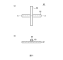
- FIG. 11(a) is a plan view of a quantum bit element in Example 4, and
- FIG. 11(b) is a cross-sectional view taken along line AA of FIG. 11(a).
- 12A to 12C are cross-sectional views (part 1) illustrating a method for manufacturing a device according to the fourth embodiment.
- 13A to 13C are cross-sectional views (part 2) illustrating a method for manufacturing a device according to the fourth embodiment.
- 14A to 14C are cross-sectional views (part 1) illustrating a method for manufacturing a quantum bit element and a seventh wiring pattern in the fourth embodiment.
- 15A to 15C are cross-sectional views (part 2) illustrating a method for manufacturing a quantum bit element and a seventh wiring pattern in the fourth embodiment.
- 16A to 16C are cross-sectional views (part 1) showing a method for manufacturing a device according to a comparative example.
- 17A to 17C are cross-sectional views (part 2) showing a method for manufacturing a device according to a comparative example.
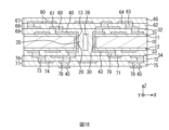
- FIG. 18 is a cross-sectional view of a case where a plurality of wiring layers are stacked on the substrate side of the quantum bit element.
- 19A to 19C are cross-sectional views showing a method for manufacturing a device according to the fifth embodiment.
- FIG. 1 is a cross-sectional view of a device according to Example 1.
- Example 1 shows an example in which device 100 is an interposer. The directions parallel to and perpendicular to first surface 11 of substrate 10 are defined as X-axis and Y-axis, and the thickness direction of substrate 10 is defined as Z-axis.
- device 100 according to Example 1 has substrate 10 having first surface 11 and second surface 12 opposite to first surface 11, and through-hole 13 penetrating between first surface 11 and second surface 12.
- Substrate 10 is, for example, a silicon substrate, a glass substrate, or a quartz substrate.
- Through-hole 13 has, for example, a diameter of about 5 ⁇ m to 15 ⁇ m and a depth of about 100 ⁇ m to 300 ⁇ m.
- a through electrode 20 is provided in the through hole 13.
- the through electrode 20 has a cylindrical shape extending from the first surface 11 along the side of the through hole 13 onto the second surface 12.
- An insulating film 30 is provided between the side of the through hole 13 and the through electrode 20.
- the through electrode 20 is made of, for example, titanium nitride, and has a thickness of, for example, about 50 nm to 150 nm.
- the insulating film 30 is made of, for example, silicon oxide, and has a thickness of, for example, 50 nm to 150 nm.
- One or more first wiring patterns 40 are provided on the first surface 11 of the substrate 10 via an insulating film 31. At least a part of the one or more first wiring patterns 40 is connected to the through electrode 20.
- the first wiring pattern 40 is formed of the same material as the through electrode 20 (e.g., titanium nitride) and has the same thickness as the through electrode 20.
- the one or more first wiring patterns 40 may include dummy wiring that does not flow current and is at ground potential when the chip mounted on the first surface 11 and the second surface 12 of the substrate 10 is in operation.
- the insulating film 31 is formed of, for example, silicon oxide and has a thickness of, for example, about 50 nm to 150 nm.
- the thickness of the first wiring pattern 40 being the same as the thickness of the through electrode 20 does not necessarily mean that they are completely the same, but rather that a difference of the order of manufacturing error is allowed.
- the thickness of the first wiring pattern 40 is 90% to 110% of the thickness of the through electrode 20, and may be 95% to 105%.
- An insulating film 32 is provided on the first surface 11 of the substrate 10, covering one or more first wiring patterns 40. Through wiring 41 is provided, embedded in an opening provided in the insulating film 32 and connected to the first wiring pattern 40.
- a first terminal electrode 42 is provided on the insulating film 32, connected to the through wiring 41 and serving as a terminal for external connection.
- the insulating film 32 is formed of, for example, silicon oxide, and has a thickness of, for example, 100 nm to 300 nm.
- the first terminal electrode 42 is formed of a high-melting point metal material, such as vanadium, molybdenum, hafnium, or tantalum.
- the through wiring 41 may be formed of the same material as the first terminal electrode 42, or may be formed of a different material.
- One or more second wiring patterns 43 are provided on the second surface 12 of the substrate 10 via an insulating film 33. At least a part of the one or more second wiring patterns 43 is connected to the through electrode 20.
- the second wiring pattern 43 is formed of the same material as the through electrode 20 (e.g., titanium nitride) and has the same thickness as the through electrode 20.
- the one or more second wiring patterns 43 may include dummy wiring that does not flow current and is at ground potential when the chip mounted on the first surface 11 and the second surface 12 of the substrate 10 is in operation.
- the insulating film 33 is formed of, for example, silicon oxide and has a thickness of, for example, about 50 nm to 150 nm.
- the thickness of the second wiring pattern 43 is not limited to being completely the same as the thickness of the through electrode 20, but allows for a difference of the order of manufacturing error.
- the thickness of the second wiring pattern 43 is 90% to 110% of the thickness of the through electrode 20, and may be 95% to 105%.
- An insulating film 34 is provided on the second surface 12 of the substrate 10, covering one or more second wiring patterns 43. Through wiring 44 is provided, embedded in an opening provided in the insulating film 34 and connected to the second wiring pattern 43.
- a second terminal electrode 45 is provided on the insulating film 34, connected to the through wiring 44 and serving as a terminal for external connection.
- a bump electrode 46 is provided on the surface of the second terminal electrode 45.
- the insulating film 34 is formed of, for example, silicon oxide, and has a thickness of, for example, 100 nm to 300 nm.
- the second terminal electrode 45 is formed of a high-melting point metal material, like the first terminal electrode 42.
- the through wiring 44 may be formed of the same material as the second terminal electrode 45, or may be formed of a different material.
- the bump electrode 46 is formed of, for example, indium, gallium, or solder.
- An insulating film 35 is provided inside the through hole 13 to cover the surface of the through electrode 20.
- a cavity 36 is formed in the through hole 13 on the central side of the insulating film 35.
- the insulating film 35 is formed of, for example, silicon oxide and has a thickness of, for example, about 25 nm to 75 nm. Note that the central side of the through hole 13 on the central side of the through electrode 20 may be filled with the insulating film 35 without forming the cavity 36, or the insulating film 35 may be filled with another film made of a different material.
- the total area of the faces 48 of the one or more first wiring patterns 40 opposite the substrate 10 is the same as the total area of the faces 49 of the one or more second wiring patterns 43 opposite the substrate 10.
- the areas being the same does not necessarily mean that they are completely the same, but rather allows for differences of the order of manufacturing error.
- the total area of the faces 48 of the one or more first wiring patterns 40 is 90% to 110% of the total area of the faces 49 of the one or more second wiring patterns 43, and may be 95% to 105%.
- the electrodes and wiring are preferably formed of a superconducting material that exhibits superconductivity at extremely low temperatures (for example, 10 Kelvin or less). That is, the first wiring pattern 40, the second wiring pattern 43, the first terminal electrode 42, the second terminal electrode 45, the through-wires 41, 44, and the bump electrodes 46 are preferably formed of a superconducting material. Examples of superconducting materials include aluminum, titanium, vanadium, zinc, gallium, zirconium, niobium, molybdenum, technetium, cadmium, indium, tin, hafnium, tantalum, niobium nitride, and titanium nitride. Furthermore, when a chip other than a quantum bit chip is implemented in device 100, the electrodes and wiring may be formed of copper, tungsten, or the like in addition to the above materials.
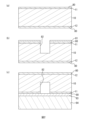
- FIG. 2(a) to 5(c) are cross-sectional views showing a method for manufacturing a device according to Example 1.
- a substrate 10 which is a silicon substrate
- the substrate 10 is heated in an oxidizing atmosphere to form a thermal oxide film 80, which is a silicon oxide film, on the first surface 11 and the second surface 12 of the substrate 10.
- the thickness of the thermal oxide film 80 is, for example, 100 nm.
- a resist is applied onto the thermal oxide film 80 formed on the first surface 11 of the substrate 10 to form a resist film 81.
- the resist film 81 is exposed to light and developed to form an opening in the resist film 81.
- a hard mask layer may be formed between the resist film 81 and the thermal oxide film 80.
- a recess 82 is formed in the substrate 10.
- the recess 82 is formed, for example, using the Bosch process.
- the recess 82 corresponds to the through hole 13 in FIG. 1 and has a diameter of, for example, 10 ⁇ m and a depth of, for example, 200 ⁇ m.
- the substrate 10 is turned upside down and the thermal oxide film 80 is bonded to a support substrate 84 with an adhesive 83.
- the support substrate 84 is, for example, a silicon substrate.
- the substrate 10 is thinned from the second surface 12 side by grinding and polishing (for example, by chemical mechanical polishing (CMP)) to expose the recess 82.
- CMP chemical mechanical polishing
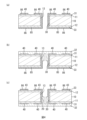
- the substrate 10 is heated in an oxidizing atmosphere to form an insulating film 33, which is a silicon oxide film, on the second surface 12 of the substrate 10, and an insulating film 30, which is a silicon oxide film, on the side surface of the through hole 13.
- the thickness of the insulating films 30 and 33 is, for example, 100 nm.
- the insulating films 30 and 33 may be formed using a chemical vapor deposition (CVD) method.
- CVD chemical vapor deposition
- a conductive film 85 extending from the first surface 11 of the substrate 10 to the second surface 12 via the side of the through hole 13 is formed by a single film formation process using, for example, atomic layer deposition (ALD).
- ALD atomic layer deposition
- a conductive film 85 made of titanium nitride is formed by ALD using Ti[N(CH 3 ) 2 ] 4 gas and NH 3 gas.
- the thickness of the conductive film 85 is, for example, 100 nm.
- N 2 H 4 gas may be used instead of NH 3 gas.
- an insulating film 86 made of a silicon oxide film covering the surface of the conductive film 85 is formed by, for example, ALD.
- the thickness of the insulating film 86 is, for example, 50 nm.
- the insulating film 86 is formed in order to suppress alteration due to exposure of the conductive film 85 and to suppress unintended conduction of the conductive film 85.
- FIG. 6 is a cross-sectional view showing an example of the formation of a conductive film in Example 1.
- the substrate 10 is placed on a support (not shown) such as a quartz basket and placed in a film formation chamber 87 of an ALD apparatus.
- Ti[N(CH 3 ) 2 ] 4 gas and NH 3 gas are introduced from the inlet In toward the outlet Out into the film formation chamber 87 to form a conductive film 85 on the substrate 10.
- a conductive film 85 of uniform thickness is formed not only on the first surface 11 of the substrate 10 but also on the second surface 12 and the side of the through hole 13.
- FIG. 6 shows an example in which the ALD apparatus is, for example, a Hot Wall ALD apparatus having a heating unit 88 beside the film formation chamber 87.
- a batch type is shown as an example, a single-wafer type may also be used.
- an opening is formed in an insulating film 86 formed on the first surface 11 of the substrate 10 by reactive ion etching (RIE) using, for example, a fluorine-based gas.
- RIE reactive ion etching
- the conductive film 85 formed on the first surface 11 of the substrate 10 is patterned by RIE using, for example, a chlorine-based gas to form one or more first wiring patterns 40.
- the first wiring patterns 40 are formed on the first surface 11 of the substrate 10 via an insulating film 31 made of a thermal oxide film 80.
- an insulating film made of a silicon oxide film is formed on the first surface 11 of the substrate 10, for example by using a CVD method, and an insulating film 32 that covers one or more first wiring patterns 40 together with an insulating film 86 is formed on the insulating film 31.
- the thickness of the insulating film 32 is, for example, 200 nm.
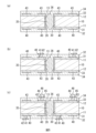
- the substrate 10 is turned upside down, and an opening is formed in the insulating film 86 formed on the second surface 12 of the substrate 10, for example, by RIE using a fluorine-based gas. Then, the conductive film 85 formed on the second surface 12 of the substrate 10 is patterned, for example, by RIE using a chlorine-based gas, to form one or more second wiring patterns 43.
- the second wiring patterns 43 are formed on the second surface 12 of the substrate 10 via the insulating film 33.
- a cylindrical through electrode 20 made of the conductive film 85 is formed on the side of the through hole 13, connected to the first wiring pattern 40 and the second wiring pattern 43.
- an insulating film made of a silicon oxide film is formed on the second surface 12 of the substrate 10, for example, by using a CVD method, and an insulating film 34 that covers one or more second wiring patterns 43 together with the insulating film 86 is formed on the insulating film 33.
- the thickness of the insulating film 34 is 200 nm.
- An insulating film 35 that covers the surface of the through electrode 20 is formed on the center side of the through hole 13 relative to the through electrode 20.
- a cavity 36 is formed on the center side of the through hole 13 relative to the insulating film 35.
- the substrate 10 is turned upside down, and an opening is formed in the insulating film 32 by, for example, RIE using a fluorine-based gas, to expose the first wiring pattern 40.
- a sputtering method is used to form a through wiring 41 that is embedded in the opening formed in the insulating film 32 and connects to the first wiring pattern 40.
- a first terminal electrode 42 that connects to the through wiring 41 is formed on the insulating film 32 by, for example, a sputtering method and an etching method.
- the through wiring 41 and the first terminal electrode 42 are not limited to being formed in separate steps, and may be formed simultaneously in the same step.
- a through wire 44 that connects to the second wiring pattern 43 is formed in the insulating film 34 by the same method as for the through wire 41 and the first terminal electrode 42, and a second terminal electrode 45 that connects to the through wire 44 is formed.
- the through wire 44 and the second terminal electrode 45 are not limited to being formed in separate processes, and may be formed simultaneously in the same process.
- a bump electrode 46 is formed on the surface of the second terminal electrode 45. In this manner, the device 100 according to the first embodiment is formed.
- the through wiring 41 and the first terminal electrode 42 are formed, and then the through wiring 44 and the second terminal electrode 45 are formed, but they may be formed in the opposite order.
- the bump electrode 46 may be formed on the first terminal electrode 42 without being formed on the second terminal electrode 45, or may be formed on both the first terminal electrode 42 and the second terminal electrode 45, or may not be formed on both.
- a conductive film 85 is formed that extends from the first surface 11 of the substrate 10 via the side of the through hole 13 onto the second surface 12.
- the conductive film 85 formed on the first surface 11 of the substrate 10 is patterned to form one or more first wiring patterns 40.
- the conductive film 85 formed on the second surface 12 of the substrate 10 is patterned to form one or more second wiring patterns 43.
- a through electrode 20 is formed from the conductive film 85 that extends from the first surface 11 onto the second surface 12 via the side of the through hole 13.
- the one or more first wiring patterns 40 formed on the first surface 11 and the one or more second wiring patterns 43 formed on the second surface 12 are formed of the same material as the through electrode 20 and have the same thickness as the through electrode 20. This allows for a reduction in manufacturing man-hours compared to when the first wiring pattern 40, the second wiring pattern 43, and the through electrode 20 are formed as separate films. This allows for a reduction in energy and materials used during manufacturing. Having the same thickness does not necessarily mean that they are completely the same, but allows for differences of the order of manufacturing error. For example, the thickness of the first wiring pattern 40 and the second wiring pattern 43 is 90% to 110% of the thickness of the through electrode 20, and may be 95% to 105%.
- Example 1 as shown in FIG. 3(c), the conductive film 85 is formed by the ALD method. This allows the conductive film 85 to be formed with the same thickness on the first surface 11, the second surface 12, and the side surface of the through hole 13 of the substrate 10, even if the aspect ratio of the through hole 13 is large.
- the first wiring pattern 40 and the second wiring pattern 43 are formed so that the total area of the surface 48 of the one or more first wiring patterns 40 opposite the substrate 10 is the same as the total area of the surface 49 of the one or more second wiring patterns 43 opposite the substrate 10. This reduces warping of the substrate 10. This improves the bonding reliability when flip-chip mounting a chip on the substrate 10, and also improves the yield in forming the first terminal electrodes 42 and the second terminal electrodes 45.
- the areas being the same does not necessarily mean that they are completely the same, but rather means that differences of the order of manufacturing error are allowed.
- the total area of the surface 48 of the one or more first wiring patterns 40 is 90% to 110% of the total area of the surface 49 of the one or more second wiring patterns 43, and may be 95% to 105%.
- Example 1 As shown in FIG. 5(b), a first terminal electrode 42 for external connection connected to one or more first wiring patterns 40 is formed on the first surface 11 of the substrate 10. As shown in FIG. 5(c), a second terminal electrode 45 for external connection connected to one or more second wiring patterns 43 is formed on the second surface 12 of the substrate 10. This allows the device 100 of Example 1 to be used as an interposer.
- the conductive film 85 is made of titanium nitride. In this way, by forming the conductive film 85 from a superconducting material, the device 100 can be used as an interposer on which a quantum bit chip is mounted.
- FIG. 7(a) and 7(b) are cross-sectional views showing a method for manufacturing a device according to Example 2.
- a quantum bit chip 50 is flip-chip mounted on a first surface 11 of a substrate 10 constituting a device 100.
- the quantum bit chip 50 is bonded to a first terminal electrode 42 by a bump electrode 52.
- a quantum bit element is formed on the quantum bit chip 50, although not shown.
- a circuit chip 51 is flip-chip mounted on a second surface 12 of the substrate 10.
- the circuit chip 51 is bonded to a second terminal electrode 45 by a bump electrode 46.
- An active element such as a CMOS element and/or a passive element such as an inductor or a capacitor is formed on the circuit chip 51, although not shown. In this way, a device 200 according to Example 2 is formed.
- a quantum bit chip 50 is mounted on the first surface 11 of the substrate 10.
- a circuit chip 51 is mounted on the second surface 12 of the substrate 10. This results in a device 200 in which the quantum bit chip 50 and the circuit chip 51 are mounted on the substrate 10. Furthermore, when the total area of the surfaces 48 of the one or more first wiring patterns 40 is the same as the total area of the surfaces 49 of the one or more second wiring patterns 43, warping of the substrate 10 is reduced, improving the reliability of the connections between the substrate 10 and the quantum bit chip 50 and the circuit chip 51.
- the circuit chip 51 may be mounted on the first surface 11 of the substrate 10, and the quantum bit chip 50 may be mounted on the second surface 12.
- FIG. 8(a) to FIG. 9(c) are cross-sectional views showing a method for manufacturing a device according to Example 3. As shown in FIG. 8(a), the same steps as those shown in FIG. 2(a) to FIG. 5(a) of Example 1 are carried out to obtain FIG. 8(a).
- an opening is formed in the insulating film 32 by RIE using, for example, a fluorine-based gas to expose the first wiring pattern 40, and a through-wire 60 is formed by, for example, a sputtering method so as to fill the opening.
- a conductive film is formed on the first surface 11 of the substrate 10 by, for example, a sputtering method, and then the conductive film is patterned by RIE using, for example, a chlorine-based gas to form one or more third wiring patterns 61.
- the third wiring pattern 61 is formed of, for example, titanium nitride.
- an insulating film 62 which is a silicon oxide film, is formed on the first surface 11 of the substrate 10 by, for example, a CVD method.
- the insulating film 62 is formed on the insulating film 32, covering the one or more third wiring patterns 61.
- a wiring layer 66 including the one or more third wiring patterns 61 and the insulating film 62 is formed.
- an opening is formed in the insulating film 62 to expose the third wiring pattern 61, and a through wiring 63 is formed to fill the opening.
- One or more fourth wiring patterns 64 connected to the through wiring 63 are formed on the insulating film 62.
- the fourth wiring pattern 64 is formed of, for example, titanium nitride.
- An insulating film 65 is formed on the insulating film 62 so as to cover the one or more fourth wiring patterns 64. This forms a wiring layer 67 including the one or more fourth wiring patterns 64 and the insulating film 65.
- the substrate 10 is turned upside down, an opening is formed in the insulating film 34 to expose the second wiring pattern 43, and the through wiring 70 is formed so as to fill the opening.
- a conductive film is formed on the second surface 12 of the substrate 10, and the conductive film is patterned to form one or more fifth wiring patterns 71.
- the fifth wiring pattern 71 is formed of, for example, the same material as the third wiring pattern 61.
- an insulating film 72 which is a silicon oxide film, is formed on the second surface 12 of the substrate 10.
- the insulating film 72 is formed on the insulating film 34, covering the one or more fifth wiring patterns 71.
- a wiring layer 76 including one or more fifth wiring patterns 71 and the insulating film 72 is formed.
- the thickness of the one or more fifth wiring patterns 71 included in the wiring layer 76 and the total area of the surface opposite to the substrate 10 are set to be the same as the thickness of the one or more third wiring patterns 61 included in the wiring layer 66 and the total area of the surface opposite to the substrate 10.
- an opening is formed in the insulating film 72 to expose the fifth wiring pattern 71, and a through wiring 73 is formed to fill the opening.
- One or more sixth wiring patterns 74 connected to the through wiring 73 are formed on the insulating film 72.
- the sixth wiring pattern 74 is formed of, for example, the same material as the fourth wiring pattern 64.
- An insulating film 75 is formed on the insulating film 72 so as to cover the one or more sixth wiring patterns 74. This forms a wiring layer 77 including one or more sixth wiring patterns 74 and the insulating film 75.
- the thickness of the one or more sixth wiring patterns 74 included in the wiring layer 77 and the total area of the surface opposite the substrate 10 are set to be the same as the thickness of the one or more fourth wiring patterns 64 included in the wiring layer 67 and the total area of the surface opposite the substrate 10.
- a through wiring 68 connected to the fourth wiring pattern 64 is formed in the insulating film 65, and a first terminal electrode 42 connected to the through wiring 68 is formed on the insulating film 65.
- a through wiring 78 connected to the sixth wiring pattern 74 is formed in the insulating film 75, and a second terminal electrode 45 connected to the through wiring 78 is formed on the insulating film 75. In this way, the device 300 according to the third embodiment is formed.
- one or more wiring layers 66, 67 are formed on the opposite side of the substrate 10 to one or more first wiring patterns 40.
- one or more wiring layers 76, 77 second wiring layers having the same number of layers as the one or more wiring layers 66, 67 are formed on the opposite side of the substrate 10 to one or more second wiring patterns 43. This makes it possible to make the number of wiring layers formed on the first surface 11 of the substrate 10 the same as the number of wiring layers formed on the second surface 12, thereby reducing warping of the substrate 10.
- one or more wiring layers 66, 67 and one or more wiring layers 76, 77 are formed so that the thickness of the wiring patterns in the same layer from the substrate 10 and the total area of the surface opposite the substrate 10 are the same. That is, one or more third wiring patterns 61 of the wiring layer 66 and one or more fifth wiring patterns 71 of the wiring layer 76, which are layers from the substrate 10, are formed so that they have the same thickness and total area on the surface opposite the substrate 10. Similarly, one or more fourth wiring patterns 64 of the wiring layer 67 and one or more sixth wiring patterns 74 of the wiring layer 77, which are layers from the substrate 10, are formed so that they have the same thickness and total area on the surface opposite the substrate 10. This can reduce warping of the substrate 10.
- the thickness and total area are not limited to being completely the same, but allow for differences of the order of manufacturing error.
- the thickness and total area of the wiring pattern on one layer may be 90% or more and 110% or less of the thickness and total area of the wiring pattern on the other layer, and may be 95% or more and 105% or less.
- FIG. 10 is a cross-sectional view of a device according to Example 4.
- a quantum bit element 90 and one or more seventh wiring patterns 91 are provided on an insulating film 32.
- the quantum bit element 90 is connected to the through electrode 20 via the seventh wiring pattern 91 and the first wiring pattern 40.
- An insulating film 37 that covers the quantum bit element 90 and the seventh wiring pattern 91 is provided on the insulating film 32.
- the insulating film 37 is, for example, a silicon oxide film, and has a thickness of, for example, 100 nm to 300 nm.
- the other configurations are the same as those in Example 1, so a description thereof will be omitted.
- the quantum bit element 90 is a Josephson junction element having a lower superconducting film 92, an insulating film 93, and an upper superconducting film 94.
- the lower superconducting film 92 and the upper superconducting film 94 extend crossing each other.
- the insulating film 93 is provided between the lower superconducting film 92 and the upper superconducting film 94 at least at the intersection of the lower superconducting film 92 and the upper superconducting film 94.
- the lower superconducting film 92 and the upper superconducting film 94 are made of a superconducting material such as aluminum.
- the insulating film 93 is made of aluminum oxide, for example.
- FIG. 12(a) to 13(c) are cross-sectional views showing a method for manufacturing a device according to Example 4. First, the same steps as those shown in Fig. 2(a) to Fig. 5(a) of Example 1 are carried out to obtain Fig. 12(a).
- the insulating film 34 is bonded to the support substrate 84 with adhesive 83.
- a mask layer (not shown) formed on the insulating film 32 is used as a mask to form an opening 95 in the insulating film 32 that exposes the first wiring pattern 40, for example, by RIE using a fluorine-based gas.
- a quantum bit element 90 and one or more seventh wiring patterns 91 are formed on an insulating film 32.
- the quantum bit element 90 is connected to the first wiring pattern 40 via the seventh wiring pattern 91.
- a method for forming the quantum bit element 90 and the seventh wiring pattern 91 will be described with reference to FIG. 14(a) to FIG. 15(c).
- FIGS. 14(a) to 15(c) are cross-sectional views showing a method for manufacturing a quantum bit element and a seventh wiring pattern in Example 4.
- a lower superconducting film 92 is formed on an insulating film 32, for example, by using a vapor deposition method.
- An insulating film 93 is formed on the lower superconducting film 92, for example, by using an ALD method.
- An upper superconducting film 94 is formed on the insulating film 93, for example, by using a vapor deposition method.
- a mask layer 96 which is, for example, a silicon oxide film, is formed on the upper superconducting film 94 by, for example, a CVD method. Then, the mask layer 96 is patterned.
- the mask layer 96 is used as a mask to etch the upper superconducting film 94 by RIE using, for example, a chlorine-based gas.
- the mask layer 96 is used as a mask to etch the insulating film 93, for example, by milling.
- the mask layer 96 is used as a mask to etch the lower superconducting film 92 by RIE using, for example, a chlorine-based gas.
- the mask layer 96 is removed. This results in the formation of the quantum bit element 90, which is made up of the lower superconducting film 92, the insulating film 93, and the upper superconducting film 94.
- the seventh wiring pattern 91 is also formed by the lower superconducting film 92, the insulating film 93, and the upper superconducting film 94.
- the quantum bit element 90 is connected to the first wiring pattern 40 via the seventh wiring pattern 91.
- an insulating film 37 made of a silicon oxide film is formed on the insulating film 32, for example, by using a CVD method.
- the thickness of the insulating film 37 is, for example, 200 nm.
- the insulating film 37 is formed on the insulating film 32, covering the quantum bit element 90 and the seventh wiring pattern 91.
- the support substrate 84 is peeled off. Then, by a method similar to that shown in FIG. 5(c) of Example 1, a through-wire 44 is formed in the insulating film 34, and a second terminal electrode 45 is formed on the through-wire 44. A bump electrode 46 is formed on the surface of the second terminal electrode 45. In this manner, the device 400 according to Example 4 is formed.
- FIG. 16(a) to 17(c) are cross-sectional views showing a method for manufacturing a device according to a comparative example.
- a substrate 110 is heated in an oxidizing atmosphere to form a thermal oxide film 180 on a first surface 111 and a second surface 112 of the substrate 110.
- a quantum bit element 190 is formed on the thermal oxide film 180 formed on the first surface 111 of the substrate 110.
- an insulating film 130 which is a silicon oxide film, is formed on the first surface 111 of the substrate 110 by, for example, a CVD method.
- the insulating film 130 is formed on the thermal oxide film 180, covering the quantum bit element 190.
- an opening 150 is formed in the insulating film 130, exposing the quantum bit element 190, for example, by RIE using a fluorine-based gas.
- a conductive film 140 is formed on the first surface 111 of the substrate 110 by, for example, a sputtering method.
- the conductive film 140 is also formed so as to be embedded in the opening 150 formed in the insulating film 130.
- the conductive film 140 is formed of, for example, titanium nitride.
- the conductive film 140 is patterned by RIE using, for example, a chlorine-based gas to form one or more wiring patterns 142. Some of the one or more wiring patterns 142 are connected to the quantum bit element 190.
- an insulating film 132 which is a silicon oxide film, is formed on the first surface 111 of the substrate 110 by, for example, a CVD method.
- the insulating film 132 is formed on the insulating film 130, covering the wiring pattern 142.
- the insulating film 130 is formed and processed, the conductive film 140 is formed and processed, and the insulating film 132 is formed.
- the insulating films 130 and 132 are formed, for example, by the CVD method. In the CVD method, the temperature of the substrate 110 reaches several hundred degrees Celsius, which may damage the quantum bit element 190.
- the conductive film 140 is formed, for example, by the sputtering method, and the insulating film 130 and the conductive film 140 are processed by RIE.
- the insulating film 130 and the conductive film 140 are irradiated with charged particles, which may also damage the quantum bit element 190. For these reasons, it is considered that the characteristics of the quantum bit element 190 are deteriorated.
- Example 4 after forming one or more first wiring patterns 40 and one or more second wiring patterns 43 as shown in FIG. 12(a), quantum bit elements 90 connected to one or more first wiring patterns 40 are formed as shown in FIG. 13(a).
- quantum bit elements 90 connected to one or more first wiring patterns 40 are formed as shown in FIG. 13(a).
- the quantum bit element 90 is formed on the first surface 11 of the substrate 10, but may be formed on the second surface 12.
- the wiring layer formed on the substrate 10 side of the quantum bit element 90 may have a multi-layer wiring structure.
- FIG. 18 is a cross-sectional view of a case where multiple wiring layers are stacked on the substrate side of the quantum bit element.
- the quantum bit element 90 is preferably formed in the wiring layer 67, which is the furthest from the substrate 10, of the multiple wiring layers 66, 67, 69 formed on the first surface 11 of the substrate 10.
- the quantum bit element 90 is preferably formed after the wiring patterns in all of the wiring layers 66, 67, 69 formed on the first surface 11 side of the substrate 10.
- FIG. 19 is a cross-sectional view showing a method for manufacturing a device according to Example 5.
- a circuit chip 51 is flip-chip mounted on the second surface 12 of a substrate 10 constituting a device 400.
- the circuit chip 51 is joined to a second terminal electrode 45 by a bump electrode 46. In this way, a device 500 according to Example 5 is formed.
- the first terminal electrode 42 may be formed on the first surface 11.
- the quantum bit chip 50 may be flip-chip mounted to the first terminal electrode 42.
- the circuit chip 51 may be flip-chip mounted to the first terminal electrode 42, and the quantum bit chip 50 may be flip-chip mounted to the second terminal electrode 45.
Landscapes
- Engineering & Computer Science (AREA)
- Manufacturing & Machinery (AREA)
- Internal Circuitry In Semiconductor Integrated Circuit Devices (AREA)
Abstract
第1面と、前記第1面とは反対の第2面と、前記第1面と前記第2面との間を貫通する貫通孔と、を有する基板に、前記第1面上から前記貫通孔の側面を経由して前記第2面上に延在する超伝導材料からなる導電膜を形成する工程と、前記第1面上の前記導電膜をパターニングして第1配線パターンを形成する工程と、前記第2面上の前記導電膜をパターニングして第2配線パターンを形成する工程と、前記第1配線パターンに接続された量子ビット素子を形成する工程と、を備えるデバイスの製造方法。
Description
本発明は、デバイスおよびデバイスの製造方法に関する。
貫通電極によって表裏の回路の導通をとる中継基板であるインターポーザが知られている。例えば、量子ビットチップをインターポーザにフリップチップ実装することが知られている(例えば特許文献1~3)。また、基板の表裏面に設けられた量子ビットと受動素子とを貫通電極で接続した構成も知られている(例えば特許文献4)。
基板の第1面に形成される第1配線パターンと、第1面とは反対の第2面に形成される第2配線パターンと、第1面と第2面の間の貫通孔に形成される貫通電極と、を別々の工程で形成すると、製造工数が増えてしまう。
1つの側面では、製造工数を削減することを目的とする。
1つの態様では、第1面と、前記第1面とは反対の第2面と、前記第1面と前記第2面との間を貫通する貫通孔と、を有する基板に、前記第1面上から前記貫通孔の側面を経由して前記第2面上に延在する超伝導材料からなる導電膜を形成する工程と、前記第1面上の前記導電膜をパターニングして第1配線パターンを形成する工程と、前記第2面上の前記導電膜をパターニングして第2配線パターンを形成する工程と、前記第1配線パターンに接続された量子ビット素子を形成する工程と、を備えるデバイスの製造方法である。
1つの態様では、第1面と、前記第1面とは反対の第2面と、前記第1面と前記第2面との間を貫通する貫通孔と、を有する基板と、前記第1面上から前記貫通孔の側面を経由して前記第2面上に延在する超伝導材料からなる貫通電極と、前記第1面上に設けられ、前記貫通電極と同じ材料で形成される第1配線パターンと、前記第2面上に設けられ、前記貫通電極と同じ材料で形成される第2配線パターンと、前記第1配線パターンに接続された量子ビット素子と、を備えるデバイスである。
1つの側面として、製造工数を削減することができる。
以下、図面を参照し、本発明の実施例について説明する。
図1は、実施例1に係るデバイスの断面図である。実施例1では、デバイス100がインターポーザである場合の例を示す。基板10の第1面11に平行で互いに直交する方向をX軸およびY軸とし、基板10の厚さ方向をZ軸とする。図1のように、実施例1に係るデバイス100は、第1面11と第1面11とは反対の第2面12とを有する基板10に、第1面11と第2面12との間を貫通する貫通孔13が設けられている。基板10は、例えばシリコン基板、ガラス基板、または石英基板である。貫通孔13は、例えば直径が5μm~15μm程度で、深さが100μm~300μm程度である。
貫通孔13に貫通電極20が設けられている。貫通電極20は、第1面11上から貫通孔13の側面に沿って第2面12上に延びた筒状形状をしている。貫通孔13の側面と貫通電極20との間には絶縁膜30が設けられている。貫通電極20は、例えば窒化チタンにより形成され、厚さが例えば50nm~150nm程度である。絶縁膜30は、例えば酸化シリコンにより形成され、厚さが例えば50nm~150nmである。
基板10の第1面11上に絶縁膜31を介して1または複数の第1配線パターン40が設けられている。1または複数の第1配線パターン40のうちの少なくとも一部は貫通電極20に接続されている。第1配線パターン40は、貫通電極20と同じ材料(例えば窒化チタン)により形成され、貫通電極20と同じ厚さを有する。1または複数の第1配線パターン40には、基板10の第1面11および第2面12上に搭載されたチップの動作時に電流が流れず、グランド電位となるダミー配線が含まれていてもよい。絶縁膜31は、例えば酸化シリコンにより形成され、厚さが例えば50nm~150nm程度である。ここで、第1配線パターン40の厚さが貫通電極20の厚さと同じとは、完全に同じ場合に限られず、製造誤差程度の差を許容するものである。例えば、第1配線パターン40の厚さは、貫通電極20の厚さの90%以上110%以下であり、95%以上105%以下の場合でもよい。
基板10の第1面11上に、1または複数の第1配線パターン40を覆う絶縁膜32が設けられている。絶縁膜32に設けられた開口に埋め込まれ、第1配線パターン40に接続した貫通配線41が設けられている。絶縁膜32上に、貫通配線41に接続し、外部接続用の端子となる第1端子電極42が設けられている。絶縁膜32は、例えば酸化シリコンにより形成され、厚さが例えば100nm~300nmである。第1端子電極42は、例えばバナジウム、モリブデン、ハフニウム、またはタンタルなどの高融点金属材料により形成される。貫通配線41は、第1端子電極42と同じ材料で形成されてもよいし、異なる材料で形成されてもよい。
基板10の第2面12上に絶縁膜33を介して1または複数の第2配線パターン43が設けられている。1または複数の第2配線パターン43のうちの少なくとも一部は貫通電極20に接続されている。第2配線パターン43は、貫通電極20と同じ材料(例えば窒化チタン)により形成され、貫通電極20と同じ厚さを有する。1または複数の第2配線パターン43には、基板10の第1面11および第2面12上に搭載されたチップの動作時に電流が流れず、グランド電位となるダミー配線が含まれていてもよい。絶縁膜33は、例えば酸化シリコンにより形成され、厚さが例えば50nm~150nm程度である。ここで、第2配線パターン43の厚さが貫通電極20の厚さと同じとは、完全に同じ場合に限られず、製造誤差程度の差を許容するものである。例えば、第2配線パターン43の厚さは、貫通電極20の厚さの90%以上110%以下であり、95%以上105%以下の場合でもよい。
基板10の第2面12上に、1または複数の第2配線パターン43を覆う絶縁膜34が設けられている。絶縁膜34に設けられた開口に埋め込まれ、第2配線パターン43に接続した貫通配線44が設けられている。絶縁膜34上に、貫通配線44に接続し、外部接続用の端子となる第2端子電極45が設けられている。第2端子電極45の表面にはバンプ電極46が設けられている。絶縁膜34は、例えば酸化シリコンにより形成され、厚さが例えば100nm~300nmである。第2端子電極45は、第1端子電極42と同じく、高融点金属材料により形成される。貫通配線44は、第2端子電極45と同じ材料で形成されてもよいし、異なる材料で形成されてもよい。バンプ電極46は、例えばインジウム、ガリウム、またははんだなどで形成される。
貫通孔13内に貫通電極20の表面を覆う絶縁膜35が設けられている。貫通孔13の絶縁膜35よりも中央側は空洞36が形成されている。貫通電極20が絶縁膜35で覆われることで、貫通電極20が保護され、また、意図しない導通が生じることが抑制される。絶縁膜35は、例えば酸化シリコンにより形成され、厚さが例えば25nm~75nm程度である。なお、貫通孔13の貫通電極20よりも中央側は、空洞36が形成されずに絶縁膜35で埋め込まれていてもよいし、絶縁膜35と絶縁膜35とは材料の異なる他の膜とで埋め込まれていてもよい。
1または複数の第1配線パターン40の基板10とは反対側の面48の総面積と、1または複数の第2配線パターン43の基板10とは反対側の面49の総面積と、は同じになっている。面積が同じとは、完全に同じ場合に限られず、製造誤差程度の差を許容するものである。例えば、1または複数の第1配線パターン40の面48の総面積は、1または複数の第2配線パターン43の面49の総面積の90%以上110%以下であり、95%以上105%以下の場合でもよい。
デバイス100に量子ビットチップが実装される場合、電極および配線は極低温(例えば10ケルビン以下)で超伝導が発現する超伝導材料で形成される場合が好ましい。すなわち、第1配線パターン40、第2配線パターン43、第1端子電極42、第2端子電極45、貫通配線41、44、バンプ電極46は、超伝導材料で形成される場合が好ましい。超伝導材料として、例えばアルミニウム、チタン、バナジウム、亜鉛、ガリウム、ジルコニウム、ニオブ、モリブデン、テクネチウム、カドミウム、インジウム、錫、ハフニウム、タンタル、窒化ニオブ、窒化チタンが挙げられる。また、デバイス100に量子ビットチップ以外のチップが実装される場合、電極および配線は、上記材料の他に、銅やタングステンなどにより形成されてもよい。
[製造方法]
図2(a)から図5(c)は、実施例1に係るデバイスの製造方法を示す断面図である。図2(a)のように、シリコン基板である基板10を洗浄した後、基板10を酸化性雰囲気下で加熱して、基板10の第1面11および第2面12に酸化シリコン膜である熱酸化膜80を形成する。熱酸化膜80の厚さは一例として100nmである。
図2(a)から図5(c)は、実施例1に係るデバイスの製造方法を示す断面図である。図2(a)のように、シリコン基板である基板10を洗浄した後、基板10を酸化性雰囲気下で加熱して、基板10の第1面11および第2面12に酸化シリコン膜である熱酸化膜80を形成する。熱酸化膜80の厚さは一例として100nmである。
図2(b)のように、基板10の第1面11上に形成された熱酸化膜80上にレジストを塗布してレジスト膜81を形成する。レジスト膜81に対して露光および現像を行って、レジスト膜81に開口を形成する。なお、レジスト膜81と熱酸化膜80との間にハードマスク層を形成してもよい。レジスト膜81をマスクとして、基板10に凹部82を形成する。凹部82は、例えばボッシュプロセスを用いて形成する。凹部82は、図1における貫通孔13に対応し、直径が一例として10μm、深さが一例として200μmである。
図2(c)のように、レジスト膜81を除去した後、基板10を上下反転させ、熱酸化膜80を接着剤83によって支持基板84に接合する。支持基板84は例えばシリコン基板である。
図3(a)のように、第2面12側から基板10を研削および研磨(例えば化学機械研磨(CMP:Chemical Mechanical Polishing)などを用いて薄くし、凹部82を露出させる。これにより、基板10を第1面11と第2面12との間で貫通する貫通孔13が形成される。
図3(b)のように、支持基板84を剥離した後、基板10を酸化性雰囲気下で加熱して、基板10の第2面12に酸化シリコン膜である絶縁膜33を形成し、貫通孔13の側面に酸化シリコン膜である絶縁膜30を形成する。絶縁膜30、33の厚さは一例として100nmである。なお。絶縁膜30、33は、化学気相成長(CVD:Chemical Vapor Deposition)法を用いて形成してもよい。支持基板84の剥離は、例えば紫外線照射によって接着強度が低下する接着剤83を用いている場合では、接着剤83に紫外線を照射することにより支持基板84を剥離する。
図3(c)のように、基板10を上下反転させ、例えば原子層堆積(ALD:Atomic Layer Deposition)法を用い、基板10の第1面11上から貫通孔13の側面を経由して第2面12上に延在する導電膜85を一度の成膜プロセスにより成膜する。例えば、Ti[N(CH3)2]4ガスとNH3ガスとを用いたALD法によって、窒化チタンからなる導電膜85を成膜する。導電膜85の厚さは一例として100nmである。なお、NH3ガスの代わりにN2H4ガスを用いてもよい。その後、例えばALD法を用いて、導電膜85の表面を覆う酸化シリコン膜からなる絶縁膜86を形成する。絶縁膜86の厚さは一例として50nmである。絶縁膜86は、導電膜85が露出することによる変質を抑制するため、および、導電膜85に意図しない導通が生じることを抑制するために形成する。
図6は、実施例1における導電膜の成膜の例を示す断面図である。図6のように、基板10を石英バスケットなどの支持部(不図示)に載置してALD装置の成膜室87内に配置する。その後、成膜室87内に入口Inから出口Outに向かってTi[N(CH3)2]4ガスとNH3ガスを導入して、基板10に導電膜85を成膜する。これにより、図3(c)のように、基板10の第1面11上だけでなく、第2面12上および貫通孔13の側面にも均一な膜厚の導電膜85が成膜される。なお、図6では、ALD装置が例えば成膜室87の傍に加熱ユニット88を有するHot Wall ALD装置である場合を例に示している。また、バッチ式の場合を例に示しているが、枚葉式の場合でもよい。
図4(a)のように、例えばフッ素系ガスを用いた反応性イオンエッチング(RIE:Reactive Ion Etching)により基板10の第1面11上に形成された絶縁膜86に開口を形成する。その後、例えば塩素系ガスを用いたRIEにより基板10の第1面11上に形成された導電膜85をパターニングして1または複数の第1配線パターン40を形成する。第1配線パターン40は、熱酸化膜80からなる絶縁膜31を介して基板10の第1面11上に形成される。
図4(b)のように、基板10の第1面11上に、例えCVD法を用いて、酸化シリコン膜からなる絶縁膜を成膜し、絶縁膜86と共に1または複数の第1配線パターン40を覆う絶縁膜32を絶縁膜31上に形成する。絶縁膜32の厚さは一例として200nmである。
図4(c)のように、基板10を上下反転させ、例えばフッ素系ガスを用いたRIEにより基板10の第2面12上に形成された絶縁膜86に開口を形成する。その後、例えば塩素系ガスを用いたRIEにより基板10の第2面12上に形成された導電膜85をパターニングして1または複数の第2配線パターン43を形成する。第2配線パターン43は絶縁膜33を介して基板10の第2面12上に形成される。また、貫通孔13の側面には、導電膜85からなる筒状の貫通電極20が第1配線パターン40と第2配線パターン43とに接続して形成される。
図5(a)のように、基板10の第2面12上に、例えばCVD法を用いて、酸化シリコン膜からなる絶縁膜を成膜し、絶縁膜86と共に1または複数の第2配線パターン43を覆う絶縁膜34を絶縁膜33上に形成する。絶縁膜34の厚さは一例として200nmである。貫通孔13の貫通電極20よりも中央側には、貫通電極20の表面を覆う絶縁膜35が形成される。貫通孔13の絶縁膜35よりも中央側には空洞36が形成される。
図5(b)のように、基板10を上下反転させ、例えばフッ素系ガスを用いたRIEにより、絶縁膜32に第1配線パターン40が露出する開口を形成する。その後、例えばスパッタリング法を用いて、絶縁膜32に形成した開口に埋め込まれ、第1配線パターン40に接続する貫通配線41を形成する。絶縁膜32上に、例えばスパッタリング法およびエッチング法を用いて、貫通配線41に接続する第1端子電極42を形成する。貫通配線41と第1端子電極42は、別々の工程で形成される場合に限られず、同一工程で同時に形成されてもよい。
図5(c)のように、基板10を上下反転させた後、貫通配線41と第1端子電極42と同様の方法によって、絶縁膜34に第2配線パターン43に接続する貫通配線44を形成し、貫通配線44に接続する第2端子電極45を形成する。貫通配線44と第2端子電極45は、別々の工程で形成される場合に限られず、同一工程で同時に形成されてもよい。その後、第2端子電極45の表面にバンプ電極46を形成する。以上により、実施例1に係るデバイス100が形成される。
なお、図5(b)および図5(c)では、貫通配線41と第1端子電極42を形成した後、貫通配線44と第2端子電極45を形成する場合を例に示したが、反対の順番で形成されてもよい。バンプ電極46は、第2端子電極45には形成されず、第1端子電極42に形成されてもよいし、第1端子電極42と第2端子電極45の両方に形成されてもよいし、両方に形成されなくてもよい。
以上のように、実施例1によれば、図3(c)のように、基板10の第1面11上から貫通孔13の側面を経由して第2面12上に延在する導電膜85を形成する。図4(a)のように、基板10の第1面11上に形成された導電膜85をパターニングして1または複数の第1配線パターン40を形成する。図4(c)のように、基板10の第2面12上に形成された導電膜85をパターニングして1または複数の第2配線パターン43を形成する。第1面11上から貫通孔13の側面を経由して第2面12上に延在する導電膜85からなる貫通電極20が形成される。したがって、実施例1では、第1面11上に形成された1または複数の第1配線パターン40と第2面12上に形成された1または複数の第2配線パターン43は、貫通電極20と同じ材料で形成され、貫通電極20と同じ厚さを有する。これにより、第1配線パターン40と第2配線パターン43と貫通電極20とを別々に成膜して形成する場合に比べて、製造工数を削減することができる。よって、製造時のエネルギーおよび使用材料などを削減することができる。同じ厚さを有するとは、完全に同じ場合に限られず、製造誤差程度の差を許容するものである。例えば、第1配線パターン40および第2配線パターン43の厚さは、貫通電極20の厚さの90%以上110%以下であり、95%以上105%以下の場合でもよい。
また、実施例1では、図3(c)のように、ALD法により導電膜85を形成する。これにより、貫通孔13のアスペクト比が大きい場合でも、基板10の第1面11、第2面12、および貫通孔13の側面に同じ厚さの導電膜85を形成できる。
また、実施例1では、図1のように、1または複数の第1配線パターン40の基板10とは反対側の面48の総面積と1または複数の第2配線パターン43の基板10とは反対側の面49の総面積とが同じになるように、第1配線パターン40および第2配線パターン43を形成する。これにより、基板10に生じる反りを低減することができる。よって、基板10にチップをフリップチップ実装するときの接合信頼性を向上させることができる、また、第1端子電極42および第2端子電極45の形成での歩留まりを向上させることができる。面積が同じとは、完全に同じである場合に限られず、製造誤差程度の差を許容するものである。例えば、1または複数の第1配線パターン40の面48の総面積は、1または複数の第2配線パターン43の面49の総面積の90%以上110%以下であり、95%以上105%以下の場合でもよい。
また、実施例1では、図5(b)のように、基板10の第1面11上に、1または複数の第1配線パターン40に接続した外部接続用の第1端子電極42を形成する。図5(c)のように、基板10の第2面12上に、1または複数の第2配線パターン43に接続した外部接続用の第2端子電極45を形成する。これにより、実施例1のデバイス100をインターポーザとして用いることができる。
また、実施例1では、導電膜85は窒化チタンにより形成される。このように、導電膜85を超伝導材料により形成することで、デバイス100を量子ビットチップが実装されるインターポーザとして用いることができる。
図7(a)および図7(b)は、実施例2に係るデバイスの製造方法を示す断面図である。図7(a)のように、デバイス100を構成する基板10の第1面11上に量子ビットチップ50をフリップチップ実装する。量子ビットチップ50はバンプ電極52によって第1端子電極42に接合される。量子ビットチップ50には、図示を省略するが、量子ビット素子が形成されている。図7(b)のように、基板10の第2面12上に回路チップ51をフリップチップ実装する。回路チップ51はバンプ電極46によって第2端子電極45に接合される。回路チップ51には、図示を省略するが、例えばCMOS素子などの能動素子および/またはインダクタやキャパシタなどの受動素子が形成されている。これにより、実施例2に係るデバイス200が形成される。
実施例2によれば、図7(a)のように、基板10の第1面11上に量子ビットチップ50を搭載する。図7(b)のように、基板10の第2面12上に回路チップ51を搭載する。これにより、基板10に量子ビットチップ50と回路チップ51が搭載されたデバイス200が得られる。また、1または複数の第1配線パターン40の面48の総面積と、1または複数の第2配線パターン43の面49の総面積と、が同じ場合では、基板10の反りが低減されるため、基板10と量子ビットチップ50および回路チップ51との接合信頼性が向上する。
なお、実施例2において、基板10の第1面11上に回路チップ51が搭載され、第2面12上に量子ビットチップ50が搭載される場合でもよい。
図8(a)から図9(c)は、実施例3に係るデバイスの製造方法を示す断面図である。図8(a)のように、実施例1の図2(a)から図5(a)と同様の工程を実施して図8(a)とする。
図8(b)のように、例えばフッ素系ガスを用いたRIEによって絶縁膜32に第1配線パターン40が露出する開口を形成し、開口を埋め込むように例えばスパッタリング法を用いて貫通配線60を形成する。その後、基板10の第1面11上に、例えばスパッタリング法を用いて導電膜を成膜した後、例えば塩素系ガスを用いたRIEによって導電膜をパターニングして1または複数の第3配線パターン61を形成する。第3配線パターン61は、例えば窒化チタンにより形成される。次いで、基板10の第1面11上に例えばCVD法によって酸化シリコン膜である絶縁膜62を成膜する。絶縁膜62は1または複数の第3配線パターン61を覆って絶縁膜32上に形成される。これにより、1または複数の第3配線パターン61と絶縁膜62とを含む配線層66が形成される。
図8(c)のように、絶縁膜62に第3配線パターン61が露出する開口を形成し、開口を埋め込むように貫通配線63を形成する。絶縁膜62上に貫通配線63に接続する1または複数の第4配線パターン64を形成する。第4配線パターン64は、例えば窒化チタンにより形成される。1または複数の第4配線パターン64を覆うように絶縁膜62上に絶縁膜65を形成する。これにより、1または複数の第4配線パターン64と絶縁膜65とを含む配線層67が形成される。
図9(a)のように、基板10を上下反転させ、絶縁膜34に第2配線パターン43が露出する開口を形成し、開口を埋め込むように貫通配線70を形成する。その後、基板10の第2面12上に導電膜を成膜した後、導電膜をパターニングして1または複数の第5配線パターン71を形成する。第5配線パターン71は、例えば第3配線パターン61と同じ材料により形成される。次いで、基板10の第2面12上に酸化シリコン膜である絶縁膜72を成膜する。絶縁膜72は1または複数の第5配線パターン71を覆って絶縁膜34上に形成される。これにより、1または複数の第5配線パターン71と絶縁膜72とを含む配線層76が形成される。配線層76に含まれる1または複数の第5配線パターン71の厚さおよび基板10とは反対側の面の総面積は、配線層66に含まれる1または複数の第3配線パターン61の厚さおよび基板10とは反対側の面の総面積と同じになるようにする。
図9(b)のように、絶縁膜72に第5配線パターン71が露出する開口を形成し、開口を埋め込むように貫通配線73を形成する。絶縁膜72上に貫通配線73に接続する1または複数の第6配線パターン74を形成する。第6配線パターン74は、例えば第4配線パターン64と同じ材料により形成される。1または複数の第6配線パターン74を覆うように絶縁膜72上に絶縁膜75を形成する。これにより、1または複数の第6配線パターン74と絶縁膜75とを含む配線層77が形成される。配線層77に含まれる1または複数の第6配線パターン74の厚さおよび基板10とは反対側の面の総面積は、配線層67に含まれる1または複数の第4配線パターン64の厚さおよび基板10とは反対側の面の総面積と同じになるようにする。
図9(c)のように、図5(b)および図5(c)に示した方法と同様の方法によって、絶縁膜65に第4配線パターン64に接続する貫通配線68を形成し、絶縁膜65上に貫通配線68に接続する第1端子電極42を形成する。絶縁膜75に第6配線パターン74に接続する貫通配線78を形成し、絶縁膜75上に貫通配線78に接続する第2端子電極45を形成する。以上により、実施例3に係るデバイス300が形成される。
実施例3によれば、図8(b)および図8(c)のように、1または複数の第1配線パターン40に対して基板10とは反対側に、1または複数層の配線層66、67(第1配線層)を形成する。図9(a)および図9(b)のように、1または複数の第2配線パターン43に対して基板10とは反対側に、1または複数層の配線層66、67と同じ層数の1または複数層の配線層76、77(第2配線層)を形成する。これにより、基板10の第1面11上に形成された配線層の層数と、第2面12上に形成された配線層の層数と、を同じにできるため、基板10の反りを低減することができる。
また、実施例3では、基板10からの層数が同じ層における配線パターンの厚さおよび基板10とは反対側の面の総面積が同じになるように、1または複数層の配線層66、67および1または複数層の配線層76、77を形成する。すなわち、基板10からの層数が同じ層である配線層66の1または複数の第3配線パターン61と配線層76の1または複数の第5配線パターン71とは、厚さおよび基板10とは反対側の総面積が同じなるように形成する。同様に、基板10からの層数が同じ層である配線層67の1または複数の第4配線パターン64と配線層77の1または複数の第6配線パターン74とは、厚さおよび基板10とは反対側の総面積が同じなるように形成する。これにより、基板10の反りを低減することができる。厚さおよび総面積が同じとは、完全に同じ場合に限られず、製造誤差程度の差を許容するものである。例えば、一方の層における配線パターンの厚さおよび総面積は、他方の層における配線パターンの厚さおよび総面積の90%以上110%以下であり、95%以上105%以下の場合でもよい。
実施例4では量子ビット素子が形成された量子ビットデバイスの場合の例を示す。図10は、実施例4に係るデバイスの断面図である。図10のように、実施例4に係るデバイス400では、絶縁膜32上に、量子ビット素子90と1または複数の第7配線パターン91が設けられている。量子ビット素子90は第7配線パターン91と第1配線パターン40を介して貫通電極20に接続されている。絶縁膜32上に、量子ビット素子90および第7配線パターン91を覆う絶縁膜37が設けられている。絶縁膜37は、例えば酸化シリコン膜であり、厚さは例えば100nm~300nmである。その他の構成は、実施例1と同じであるため説明を省略する。
図11(a)は、実施例4における量子ビット素子の平面図、図11(b)は、図11(a)のA-A断面図である。図11(a)および図11(b)のように、量子ビット素子90は、下層超伝導膜92と絶縁膜93と上層超伝導膜94とを有するジョセフソン接合素子である。下層超伝導膜92と上層超伝導膜94とは互いに交差して伸びている。絶縁膜93は、少なくとも下層超伝導膜92と上層超伝導膜94とが交差する箇所で、下層超伝導膜92と上層超伝導膜94との間に設けられている。下層超伝導膜92および上層超伝導膜94は例えばアルミニウムなどの超伝導材料により形成される。絶縁膜93は例えば酸化アルミニウムにより形成される。
[製造方法]
図12(a)から図13(c)は、実施例4に係るデバイスの製造方法を示す断面図である。まず、実施例1の図2(a)から図5(a)と同じ工程を実施して図12(a)とする。
図12(a)から図13(c)は、実施例4に係るデバイスの製造方法を示す断面図である。まず、実施例1の図2(a)から図5(a)と同じ工程を実施して図12(a)とする。
図12(b)のように、絶縁膜34を接着剤83によって支持基板84に接合する。
図12(c)のように、絶縁膜32上に形成したマスク層(不図示)をマスクとして、例えばフッ素系ガスを用いたRIEにより、絶縁膜32に第1配線パターン40を露出する開口95を形成する。
図13(a)のように、絶縁膜32上に量子ビット素子90と1または複数の第7配線パターン91を形成する。量子ビット素子90は第7配線パターン91を介して第1配線パターン40に接続される。ここで、量子ビット素子90と第7配線パターン91の形成方法について図14(a)から図15(c)を用いて説明する。
図14(a)から図15(c)は、実施例4における量子ビット素子および第7配線パターンの製造方法を示す断面図である。図14(a)のように、絶縁膜32上に、例えば蒸着法を用いて、下層超伝導膜92を成膜する。下層超伝導膜92上に、例えばALD法を用いて、絶縁膜93を成膜する。絶縁膜93上に、例えば蒸着法を用いて、上層超伝導膜94を成膜する。
図14(b)のように、上層超伝導膜94上に、例えばCVD法を用いて、例えば酸化シリコン膜であるマスク層96を成膜する。その後、マスク層96をパターニングする。
図14(c)のように、マスク層96をマスクとし、例えば塩素系ガスを用いたRIEにより上層超伝導膜94をエッチングする。
図15(a)のように、マスク層96をマスクとし、例えばミリング法を用いて絶縁膜93をエッチングする。
図15(b)のように、マスク層96をマスクとし、例えば塩素系ガスを用いたRIEにより下層超伝導膜92をエッチングする。
図15(c)のように、マスク層96を除去する。これにより、下層超伝導膜92と絶縁膜93と上層超伝導膜94とにより形成される量子ビット素子90が形成される。また、下層超伝導膜92と絶縁膜93と上層超伝導膜94とにより第7配線パターン91も形成される。量子ビット素子90は第7配線パターン91を介して第1配線パターン40に接続する。
図13(b)のように、絶縁膜32上に、例えばCVD法を用いて、酸化シリコン膜からなる絶縁膜37を成膜する。絶縁膜37の厚さは一例として200nmである。絶縁膜37は量子ビット素子90および第7配線パターン91を覆って絶縁膜32上に形成される。
図13(c)のように、支持基板84を剥離する。その後、実施例1の図5(c)と同様な方法によって、絶縁膜34に貫通配線44を形成し、貫通配線44上に第2端子電極45を形成する。第2端子電極45の表面にバンプ電極46を形成する。以上により、実施例4に係るデバイス400が形成される。
[比較例]
図16(a)から図17(c)は、比較例に係るデバイスの製造方法を示す断面図である。図16(a)のように、基板110を酸化性雰囲気下で加熱して、基板110の第1面111および第2面112に熱酸化膜180を形成する。次いで、基板110の第1面111上に形成された熱酸化膜180上に量子ビット素子190を形成する。
図16(a)から図17(c)は、比較例に係るデバイスの製造方法を示す断面図である。図16(a)のように、基板110を酸化性雰囲気下で加熱して、基板110の第1面111および第2面112に熱酸化膜180を形成する。次いで、基板110の第1面111上に形成された熱酸化膜180上に量子ビット素子190を形成する。
図16(b)のように、基板110の第1面111上に、例えばCVD法により、酸化シリコン膜である絶縁膜130を成膜する。絶縁膜130は、量子ビット素子190を覆って熱酸化膜180上に形成される。
図16(c)のように、例えばフッ素系ガスを用いたRIEにより、絶縁膜130に量子ビット素子190が露出する開口150を形成する。
図17(a)のように、基板110の第1面111上に、例えばスパッタリング法を用いて、導電膜140を成膜する。導電膜140は、絶縁膜130に形成された開口150にも埋め込まれて形成される。導電膜140は、例えば窒化チタンにより形成される。
図17(b)のように、例えば塩素系ガスを用いたRIEにより、導電膜140をパターニングして1または複数の配線パターン142を形成する。1または複数の配線パターン142のうちの一部は量子ビット素子190に接続される。
図17(c)のように、基板110の第1面111上に、例えばCVD法により、酸化シリコン膜である絶縁膜132を成膜する。絶縁膜132は、配線パターン142を覆って絶縁膜130上に形成される。
複数の配線パターンが積層された多層配線構造を形成する場合では、図16(c)から図17(c)に示した工程を繰り返し行う。
比較例によれば、図16(a)から図17(c)のように、量子ビット素子190を形成した後、絶縁膜130の成膜および加工、導電膜140の成膜および加工、絶縁膜132の成膜を行っている。絶縁膜130、132は例えばCVD法により成膜される。CVD法による成膜では、基板110が数百℃の温度になるため、量子ビット素子190にダメージを与える恐れがある。また、導電膜140の成膜は例えばスパッタリング法で行い、絶縁膜130および導電膜140の加工はRIEにより行われる。スパッタリング法およびRIEでは、絶縁膜130および導電膜140に荷電粒子が照射されるため、量子ビット素子190にもダメージを与える恐れがある。これらのことから、量子ビット素子190の特性が劣化してしまうことが考えられる。
一方、実施例4によれば、図12(a)のように、1または複数の第1配線パターン40および1または複数の第2配線パターン43を形成した後、図13(a)のように、1または複数の第1配線パターン40に接続される量子ビット素子90を形成する。このように、量子ビット素子90を第1配線パターン40および第2配線パターン43よりも後に形成することで、量子ビット素子90に与えるダメージを低減することができる。よって、量子ビット素子90の特性劣化を抑制でき、量子ビット素子90の動作を安定させることができる。
なお、実施例4では、量子ビット素子90は、基板10の第1面11上に形成される場合を例に示したが、第2面12上に形成される場合でもよい。また、実施例4において、量子ビット素子90よりも基板10側に形成される配線層は多層配線構造であってもよい。
図18は、量子ビット素子より基板側に複数の配線層が積層された場合の断面図である。図18のように、量子ビット素子90は、基板10の第1面11上に形成される複数の配線層66、67、69のうちの最も基板10から離れた配線層67に形成される場合が好ましい。すなわち、量子ビット素子90は、基板10の第1面11側に形成される配線層66、67、69の全てにおける配線パターンよりも後に形成されることが好ましい。量子ビット素子90を全ての配線パターンより後に形成することで、量子ビット素子90に与えるダメージを低減でき、かつ、配線プロセスでのアニール処理の温度を高くすることができる。
図19は、実施例5に係るデバイスの製造方法を示す断面図である。図19のように、デバイス400を構成する基板10の第2面12上に回路チップ51をフリップチップ実装する。回路チップ51はバンプ電極46によって第2端子電極45に接合される。これにより、実施例5に係るデバイス500が形成される。
なお、デバイス400において、基板10の第2面12上に第2端子電極45が形成されることに加え、第1面11上に第1端子電極42が形成される場合でもよい。この場合、第1端子電極42に量子ビットチップ50がフリップチップ実装されてもよい。また、第1端子電極42に回路チップ51がフリップチップ実装され、第2端子電極45に量子ビットチップ50がフリップチップ実装される場合でもよい。
以上、本発明の実施例について詳述したが、本発明はかかる特定の実施例に限定されるものではなく、特許請求の範囲に記載された本発明の要旨の範囲内において、種々の変形・変更が可能である。
10…基板、11…第1面、12…第2面、13…貫通孔、20…貫通電極、30、31、32、33、34、35…絶縁膜、36…空洞、37…絶縁膜、40…第1配線パターン、41…貫通配線、42…第1端子電極、43…第2配線パターン、44…貫通配線、45…第2端子電極、46…バンプ電極、48、49…面、50…量子ビットチップ、51…回路チップ、52…バンプ電極、60…貫通配線、61…第3配線パターン、62…絶縁膜、63…貫通配線、64…第4配線パターン、65…絶縁膜、66、67…配線層、68…貫通配線、70…貫通配線、71…第5配線パターン、72…絶縁膜、73…貫通配線、74…第6配線パターン、75…絶縁膜、76、77…配線層、78…貫通配線、80…熱酸化膜、81…レジスト膜、82…凹部、83…接着剤、84…支持基板、85…導電膜、86…絶縁膜、87…成膜室、88…加熱ユニット、90…量子ビット素子、91…第7配線パターン、92…下層超伝導膜、93…絶縁膜、94…上層超伝導膜、95…開口、96…マスク層、100…デバイス、110…基板、111…第1面、112…第2面、130、132…絶縁膜、140…導電膜、142…配線パターン、150…開口、180…熱酸化膜、190…量子ビット素子、200、300、400、500…デバイス
Claims (8)
- 第1面と、前記第1面とは反対の第2面と、前記第1面と前記第2面との間を貫通する貫通孔と、を有する基板に、前記第1面上から前記貫通孔の側面を経由して前記第2面上に延在する超伝導材料からなる導電膜を形成する工程と、
前記第1面上の前記導電膜をパターニングして第1配線パターンを形成する工程と、
前記第2面上の前記導電膜をパターニングして第2配線パターンを形成する工程と、
前記第1配線パターンに接続された量子ビット素子を形成する工程と、を備えるデバイスの製造方法。 - 前記導電膜を形成する工程は、原子層堆積法により前記導電膜を形成する、請求項1に記載のデバイスの製造方法。
- 前記第1配線パターンを形成する工程、および、前記第2配線パターンを形成する工程は、前記第1配線パターンの前記基板とは反対側の面の総面積と前記第2配線パターンの前記基板とは反対側の面の総面積とが同じになるように、前記第1配線パターン、および、前記第2配線パターンを形成する、請求項1または2に記載のデバイスの製造方法。
- 前記第1配線パターンに対して前記基板とは反対側に、1または複数層の第1配線層を形成する工程と、
前記第2配線パターンに対して前記基板とは反対側に、前記1または複数層の第1配線層と同じ層数の1または複数層の第2配線層を形成する工程と、を備える、請求項1または2に記載のデバイスの製造方法。 - 前記1または複数層の第1配線層を形成する工程、および、前記1または複数層の第2配線層を形成する工程は、前記基板からの層数が同じ層における配線パターンの厚さおよび前記基板とは反対側の面の総面積が同じになるように、前記1または複数層の第1配線層、および、前記1または複数層の第2配線層を形成する、請求項4に記載のデバイスの製造方法。
- 前記第1面上に、前記第1配線パターンの少なくとも1つに接続された外部接続用の第1端子電極を形成する工程と、
前記第2面上に、前記第2配線パターンの少なくとも1つに接続された外部接続用の第2端子電極を形成する工程と、を備える、請求項1または2に記載のデバイスの製造方法。 - 前記第1面および前記第2面のうち一方の面上に量子ビットチップを搭載する工程と、
前記第1面および前記第2面のうち他方の面上に回路チップを搭載する工程と、を備える、請求項6に記載のデバイスの製造方法。 - 第1面と、前記第1面とは反対の第2面と、前記第1面と前記第2面との間を貫通する貫通孔と、を有する基板と、
前記第1面上から前記貫通孔の側面を経由して前記第2面上に延在する超伝導材料からなる貫通電極と、
前記第1面上に設けられ、前記貫通電極と同じ材料で形成される第1配線パターンと、
前記第2面上に設けられ、前記貫通電極と同じ材料で形成される第2配線パターンと、
前記第1配線パターンに接続された量子ビット素子と、を備えるデバイス。
Priority Applications (4)
| Application Number | Priority Date | Filing Date | Title |
|---|---|---|---|
| EP23917567.2A EP4654808A4 (en) | 2023-01-20 | 2023-01-20 | DEVICE AND DEVICE PRODUCTION METHOD |
| PCT/JP2023/001769 WO2024154354A1 (ja) | 2023-01-20 | 2023-01-20 | デバイスおよびデバイスの製造方法 |
| JP2024571592A JPWO2024154354A1 (ja) | 2023-01-20 | 2023-01-20 | |
| US19/227,604 US20250301921A1 (en) | 2023-01-20 | 2025-06-04 | Device and method of manufacturing device |
Applications Claiming Priority (1)
| Application Number | Priority Date | Filing Date | Title |
|---|---|---|---|
| PCT/JP2023/001769 WO2024154354A1 (ja) | 2023-01-20 | 2023-01-20 | デバイスおよびデバイスの製造方法 |
Related Child Applications (1)
| Application Number | Title | Priority Date | Filing Date |
|---|---|---|---|
| US19/227,604 Continuation US20250301921A1 (en) | 2023-01-20 | 2025-06-04 | Device and method of manufacturing device |
Publications (1)
| Publication Number | Publication Date |
|---|---|
| WO2024154354A1 true WO2024154354A1 (ja) | 2024-07-25 |
Family
ID=91955781
Family Applications (1)
| Application Number | Title | Priority Date | Filing Date |
|---|---|---|---|
| PCT/JP2023/001769 Ceased WO2024154354A1 (ja) | 2023-01-20 | 2023-01-20 | デバイスおよびデバイスの製造方法 |
Country Status (4)
| Country | Link |
|---|---|
| US (1) | US20250301921A1 (ja) |
| EP (1) | EP4654808A4 (ja) |
| JP (1) | JPWO2024154354A1 (ja) |
| WO (1) | WO2024154354A1 (ja) |
Citations (7)
| Publication number | Priority date | Publication date | Assignee | Title |
|---|---|---|---|---|
| US20180013052A1 (en) * | 2015-07-23 | 2018-01-11 | Massachusetts Institute Of Technology | Qubit and Coupler Circuit Structures and Coupling Techniques |
| WO2018212041A1 (ja) | 2017-05-16 | 2018-11-22 | 国立研究開発法人産業技術総合研究所 | 量子ビットデバイス |
| US20200343434A1 (en) | 2019-04-29 | 2020-10-29 | International Business Machines Corporation | Through-silicon-via fabrication in planar quantum devices |
| JP2021504956A (ja) * | 2017-11-30 | 2021-02-15 | インターナショナル・ビジネス・マシーンズ・コーポレーションInternational Business Machines Corporation | 共振器構造、共振器構造形成方法および共振器 |
| WO2021245949A1 (ja) | 2020-06-05 | 2021-12-09 | 日本電気株式会社 | 量子デバイス及び量子計算機 |
| US20220199507A1 (en) | 2020-12-22 | 2022-06-23 | International Business Machines Corporation | Multi-layered packaging for superconducting quantum circuits |
| JP2022167705A (ja) * | 2021-04-23 | 2022-11-04 | 日本電気株式会社 | 量子デバイス |
Family Cites Families (1)
| Publication number | Priority date | Publication date | Assignee | Title |
|---|---|---|---|---|
| US10242968B2 (en) * | 2015-11-05 | 2019-03-26 | Massachusetts Institute Of Technology | Interconnect structure and semiconductor structures for assembly of cryogenic electronic packages |
-
2023
- 2023-01-20 EP EP23917567.2A patent/EP4654808A4/en active Pending
- 2023-01-20 JP JP2024571592A patent/JPWO2024154354A1/ja active Pending
- 2023-01-20 WO PCT/JP2023/001769 patent/WO2024154354A1/ja not_active Ceased
-
2025
- 2025-06-04 US US19/227,604 patent/US20250301921A1/en active Pending
Patent Citations (7)
| Publication number | Priority date | Publication date | Assignee | Title |
|---|---|---|---|---|
| US20180013052A1 (en) * | 2015-07-23 | 2018-01-11 | Massachusetts Institute Of Technology | Qubit and Coupler Circuit Structures and Coupling Techniques |
| WO2018212041A1 (ja) | 2017-05-16 | 2018-11-22 | 国立研究開発法人産業技術総合研究所 | 量子ビットデバイス |
| JP2021504956A (ja) * | 2017-11-30 | 2021-02-15 | インターナショナル・ビジネス・マシーンズ・コーポレーションInternational Business Machines Corporation | 共振器構造、共振器構造形成方法および共振器 |
| US20200343434A1 (en) | 2019-04-29 | 2020-10-29 | International Business Machines Corporation | Through-silicon-via fabrication in planar quantum devices |
| WO2021245949A1 (ja) | 2020-06-05 | 2021-12-09 | 日本電気株式会社 | 量子デバイス及び量子計算機 |
| US20220199507A1 (en) | 2020-12-22 | 2022-06-23 | International Business Machines Corporation | Multi-layered packaging for superconducting quantum circuits |
| JP2022167705A (ja) * | 2021-04-23 | 2022-11-04 | 日本電気株式会社 | 量子デバイス |
Non-Patent Citations (2)
| Title |
|---|
| MALLEK JUSTIN L, YOST DONNA-RUTH W, ROSENBERG DANNA, YODER JONILYN L, CALUSINE GREGORY, COOK MATT, DAS RABINDRA, DAY ALEXANDRA, GO: "Fabrication of superconducting through-silicon vias", ARXIV.ORG, CORNELL UNIVERSITY LIBRARY, ARXIV.ORG, 15 March 2021 (2021-03-15), pages 1 - 14, XP093192677, Retrieved from the Internet <URL:https://arxiv.org/pdf/2103.08536> DOI: 10.48550/arxiv.2103.08536 * |
| See also references of EP4654808A1 |
Also Published As
| Publication number | Publication date |
|---|---|
| US20250301921A1 (en) | 2025-09-25 |
| EP4654808A1 (en) | 2025-11-26 |
| JPWO2024154354A1 (ja) | 2024-07-25 |
| EP4654808A4 (en) | 2026-03-04 |
Similar Documents
| Publication | Publication Date | Title |
|---|---|---|
| JP4564166B2 (ja) | ウエハ・パッシベーション層の形成方法 | |
| JP5596919B2 (ja) | 半導体装置の製造方法 | |
| JP5313626B2 (ja) | 電子部品内蔵基板及びその製造方法 | |
| TWI497660B (zh) | 具有穿透基板互連之半導體構造,以及形成穿透基板互連之方法 | |
| CN109390305B (zh) | 一种键合晶圆及其制备方法 | |
| JP2004128063A (ja) | 半導体装置及びその製造方法 | |
| JPH11274407A (ja) | 電子コンポ―ネント構造および薄膜多層キャパシタの製造方法 | |
| TWI807087B (zh) | 半導體裝置結構及其製造方法 | |
| JP2010045371A (ja) | 導電性保護膜を有する貫通電極構造体及びその形成方法 | |
| TWI701775B (zh) | 半導體結構及其製造方法 | |
| CN112420647A (zh) | 半导体装置及其制造方法 | |
| US8173539B1 (en) | Method for fabricating metal redistribution layer | |
| JP2007036060A (ja) | 半導体装置及びその製造方法 | |
| CN116998004A (zh) | 半导体装置的制造方法、半导体装置、集成电路元件及集成电路元件的制造方法 | |
| KR100787371B1 (ko) | 전극 및 반도체 장치 제조 방법 | |
| JP2007157844A (ja) | 半導体装置、および半導体装置の製造方法 | |
| WO2024154354A1 (ja) | デバイスおよびデバイスの製造方法 | |
| TWI574597B (zh) | 無核心層封裝基板與其製造方法 | |
| WO2024154358A1 (ja) | デバイスおよびデバイスの製造方法 | |
| TWI729643B (zh) | 密距配線和電容器 | |
| CN111261602B (zh) | 半导体结构的互连方法与半导体结构 | |
| WO2011148444A1 (ja) | 半導体装置及びその製造方法 | |
| CN112466831A (zh) | 半导体装置封装及其制造方法 | |
| JP2013251436A (ja) | 半導体装置の製造方法 | |
| TWI509761B (zh) | 矽基基板及其製作方法 |
Legal Events
| Date | Code | Title | Description |
|---|---|---|---|
| 121 | Ep: the epo has been informed by wipo that ep was designated in this application |
Ref document number: 23917567 Country of ref document: EP Kind code of ref document: A1 |
|
| WWE | Wipo information: entry into national phase |
Ref document number: 2024571592 Country of ref document: JP |
|
| NENP | Non-entry into the national phase |
Ref country code: DE |
|
| WWP | Wipo information: published in national office |
Ref document number: 2023917567 Country of ref document: EP |