WO2024154827A1 - 窒化珪素基板およびそれを用いた窒化珪素回路基板 - Google Patents
窒化珪素基板およびそれを用いた窒化珪素回路基板 Download PDFInfo
- Publication number
- WO2024154827A1 WO2024154827A1 PCT/JP2024/001489 JP2024001489W WO2024154827A1 WO 2024154827 A1 WO2024154827 A1 WO 2024154827A1 JP 2024001489 W JP2024001489 W JP 2024001489W WO 2024154827 A1 WO2024154827 A1 WO 2024154827A1
- Authority
- WO
- WIPO (PCT)
- Prior art keywords
- region
- silicon nitride
- area
- less
- maximum
- Prior art date
- Legal status (The legal status is an assumption and is not a legal conclusion. Google has not performed a legal analysis and makes no representation as to the accuracy of the status listed.)
- Ceased
Links
Images


Classifications
-
- H—ELECTRICITY
- H05—ELECTRIC TECHNIQUES NOT OTHERWISE PROVIDED FOR
- H05K—PRINTED CIRCUITS; CASINGS OR CONSTRUCTIONAL DETAILS OF ELECTRIC APPARATUS; MANUFACTURE OF ASSEMBLAGES OF ELECTRICAL COMPONENTS
- H05K1/00—Printed circuits
- H05K1/02—Details
- H05K1/03—Use of materials for the substrate
- H05K1/0306—Inorganic insulating substrates, e.g. ceramic, glass
-
- H—ELECTRICITY
- H05—ELECTRIC TECHNIQUES NOT OTHERWISE PROVIDED FOR
- H05K—PRINTED CIRCUITS; CASINGS OR CONSTRUCTIONAL DETAILS OF ELECTRIC APPARATUS; MANUFACTURE OF ASSEMBLAGES OF ELECTRICAL COMPONENTS
- H05K1/00—Printed circuits
- H05K1/02—Details
- H05K1/0271—Arrangements for reducing stress or warp in rigid printed circuit boards, e.g. caused by loads, vibrations or differences in thermal expansion
-
- H—ELECTRICITY
- H05—ELECTRIC TECHNIQUES NOT OTHERWISE PROVIDED FOR
- H05K—PRINTED CIRCUITS; CASINGS OR CONSTRUCTIONAL DETAILS OF ELECTRIC APPARATUS; MANUFACTURE OF ASSEMBLAGES OF ELECTRICAL COMPONENTS
- H05K1/00—Printed circuits
- H05K1/02—Details
- H05K1/03—Use of materials for the substrate
-
- H—ELECTRICITY
- H05—ELECTRIC TECHNIQUES NOT OTHERWISE PROVIDED FOR
- H05K—PRINTED CIRCUITS; CASINGS OR CONSTRUCTIONAL DETAILS OF ELECTRIC APPARATUS; MANUFACTURE OF ASSEMBLAGES OF ELECTRICAL COMPONENTS
- H05K3/00—Apparatus or processes for manufacturing printed circuits
- H05K3/38—Improvement of the adhesion between the insulating substrate and the metal
-
- H—ELECTRICITY
- H10—SEMICONDUCTOR DEVICES; ELECTRIC SOLID-STATE DEVICES NOT OTHERWISE PROVIDED FOR
- H10W—GENERIC PACKAGES, INTERCONNECTIONS, CONNECTORS OR OTHER CONSTRUCTIONAL DETAILS OF DEVICES COVERED BY CLASS H10
- H10W70/00—Package substrates; Interposers; Redistribution layers [RDL]
- H10W70/60—Insulating or insulated package substrates; Interposers; Redistribution layers
-
- H—ELECTRICITY
- H10—SEMICONDUCTOR DEVICES; ELECTRIC SOLID-STATE DEVICES NOT OTHERWISE PROVIDED FOR
- H10W—GENERIC PACKAGES, INTERCONNECTIONS, CONNECTORS OR OTHER CONSTRUCTIONAL DETAILS OF DEVICES COVERED BY CLASS H10
- H10W70/00—Package substrates; Interposers; Redistribution layers [RDL]
- H10W70/60—Insulating or insulated package substrates; Interposers; Redistribution layers
- H10W70/67—Insulating or insulated package substrates; Interposers; Redistribution layers characterised by their insulating layers or insulating parts
- H10W70/68—Shapes or dispositions thereof
-
- H—ELECTRICITY
- H10—SEMICONDUCTOR DEVICES; ELECTRIC SOLID-STATE DEVICES NOT OTHERWISE PROVIDED FOR
- H10W—GENERIC PACKAGES, INTERCONNECTIONS, CONNECTORS OR OTHER CONSTRUCTIONAL DETAILS OF DEVICES COVERED BY CLASS H10
- H10W70/00—Package substrates; Interposers; Redistribution layers [RDL]
- H10W70/60—Insulating or insulated package substrates; Interposers; Redistribution layers
- H10W70/67—Insulating or insulated package substrates; Interposers; Redistribution layers characterised by their insulating layers or insulating parts
- H10W70/69—Insulating materials thereof
- H10W70/692—Ceramics or glasses
-
- H—ELECTRICITY
- H05—ELECTRIC TECHNIQUES NOT OTHERWISE PROVIDED FOR
- H05K—PRINTED CIRCUITS; CASINGS OR CONSTRUCTIONAL DETAILS OF ELECTRIC APPARATUS; MANUFACTURE OF ASSEMBLAGES OF ELECTRICAL COMPONENTS
- H05K2201/00—Indexing scheme relating to printed circuits covered by H05K1/00
- H05K2201/09—Shape and layout
- H05K2201/09209—Shape and layout details of conductors
- H05K2201/09654—Shape and layout details of conductors covering at least two types of conductors provided for in H05K2201/09218 - H05K2201/095
- H05K2201/098—Special shape of the cross-section of conductors, e.g. very thick plated conductors
Definitions
- the embodiments described below relate to silicon nitride substrates and silicon nitride circuit substrates using the same.
- Patent Document 1 discloses a silicon nitride substrate with a thermal conductivity of 50 W/m ⁇ K or more and a three-point bending strength of 600 MPa or more.
- ⁇ -type silicon nitride powder contained in the raw material powder grows into ⁇ -type silicon nitride crystal particles during the sintering process.
- the grown ⁇ -type silicon nitride crystal particles become intricately intertwined, which increases the strength of the silicon nitride substrate.
- the three-point bending strength of aluminum nitride substrates and aluminum oxide substrates is approximately 300 to 450 MPa.
- silicon nitride substrates with thermal conductivity of 50 W/m ⁇ K or more, and even 80 W/m ⁇ K or more, have been developed. In this way, silicon nitride substrates combine high strength with heat dissipation properties.
- Silicon nitride substrates are bonded to metal plates and used as silicon nitride circuit substrates.
- metal plates are bonded using an active metal bonding method.
- the active metal method is a bonding method that uses a bonding brazing material that contains active metals such as titanium. Large surface irregularities on silicon nitride substrates can cause poor bonding.
- Patent Document 3 discloses a silicon nitride substrate in which the height difference between the peaks and valleys on the substrate surface is 1.5 to 15 ⁇ m.
- the maximum unevenness height which is the difference between the height of the maximum convexity and the depth of the maximum concavity, is 50 ⁇ m or less.
- the portion includes a first region having a height ratio to the maximum unevenness height of 0.8 to 1.0, a second region having the height ratio of 0.5 to less than 0.8, a third region having the height ratio of 0.3 to less than 0.5, and a fourth region having the height ratio of 0 to less than 0.3.
- the ratio of the area of the first region to the total area of the first to fourth regions is 1% to 10%, the ratio of the area of the second region to the total area is 10% to 50%, the ratio of the area of the third region to the total area is 20% to 50%, and the ratio of the area of the fourth region to the total area is 10% to 60%.
- FIG. 1 is a perspective view showing an example of a silicon nitride substrate according to an embodiment.
- FIG. 4 is a schematic diagram showing an example of the maximum unevenness height.
- FIG. 2 is a plan view showing an example of an unevenness distribution on the surface of a silicon nitride substrate.
- FIG. 2 is a side view showing an example of a silicon nitride circuit substrate according to an embodiment.
- 1 is a side view showing an example of a semiconductor device according to an embodiment;
- the maximum unevenness height which is the difference between the height of the maximum convexity and the depth of the maximum concavity, is 50 ⁇ m or less.
- the portion includes a first region having a height ratio to the maximum unevenness height of 0.8 to 1.0, a second region having the height ratio of 0.5 to less than 0.8, a third region having the height ratio of 0.3 to less than 0.5, and a fourth region having the height ratio of 0 to less than 0.3.
- the ratio of the area of the first region to the total area of the first to fourth regions is 1% to 10%, the ratio of the area of the second region to the total area is 10% to 50%, the ratio of the area of the third region to the total area is 20% to 50%, and the ratio of the area of the fourth region to the total area is 10% to 60%.
- FIG. 1 is a perspective view showing an example of a silicon nitride substrate according to an embodiment.
- reference numeral 1 denotes a silicon nitride substrate
- reference numeral 2 denotes a surface.
- FIG. 1 illustrates a silicon nitride substrate 1 having a rectangular surface 2.
- the shape of surface 2 is not limited to a rectangle, and may be various shapes such as a square, a circle, a pentagon, an L-shape, or a U-shape.
- surface 2 of silicon nitride substrate 1 can be used as a surface on which a circuit portion is provided.
- the maximum unevenness height which is the difference in height between the maximum convexity and the maximum concaveity, is 50 ⁇ m or less.
- Figure 2 is a schematic diagram showing an example of the maximum unevenness height.
- reference numeral 2 denotes the surface
- reference numeral 3 denotes the maximum convexity
- reference numeral 4 denotes the maximum concave
- reference numeral 5 denotes the maximum unevenness height.
- a three-dimensional shape measuring device is used to observe the unevenness.
- the three-dimensional shape measuring device used is a Keyence VR-3000 or a device with equivalent or greater performance.
- the highest point in the 6 mm x 6 mm part is the maximum convex part 3.
- the lowest point is the maximum concave part 44.
- the difference in height between the maximum convex part 3 and the maximum concave part 4 is the maximum concave height 5.
- the position of the highest point in the 6 mm x 6 mm part in the direction perpendicular to the plane is the maximum convex part 3.
- the position of the lowest point in the 6 mm x 6 mm part in the direction perpendicular to the plane is the maximum concave depth 4.
- the maximum concave height 5 is expressed as the distance in the direction perpendicular to the plane between the maximum convex part 3 and the maximum concave depth 4.
- the direction perpendicular to the plane is the direction perpendicular to the plane 2 when the plane 2 is viewed macroscopically.
- the maximum unevenness height 5 is 50 ⁇ m or less. If the maximum unevenness height 5 is greater than 50 ⁇ m, it can cause poor bonding. Furthermore, in any 6 mm x 6 mm portion of surface 2, the maximum unevenness height 5 is 50 ⁇ m or less. In other words, no matter which 6 mm x 6 mm portion is observed, the maximum unevenness height 5 is 50 ⁇ m or less.
- the size of the area to be observed is set to 6 mm x 6 mm because this provides good measurement accuracy. If the size is wider than 6 mm x 6 mm, undulations in the board may be detected, which may reduce measurement accuracy. If the size is smaller than 6 mm x 6 mm, the number of measurements will increase, which may reduce inspection efficiency.
- first to fourth regions are present.
- the first region is a region in which the height ratio to the maximum unevenness height 5 is 0.8 or more and 1.0 or less.
- the second region is a region in which the height ratio to the maximum unevenness height 5 is 0.5 or more and less than 0.8.
- the third region is a region in which the height ratio to the maximum unevenness height 5 is 0.3 or more and less than 0.5.
- the fourth region is a region in which the height ratio to the maximum unevenness height 5 is 0 or more and less than 0.3.
- the maximum unevenness height 5 in the 6 mm x 6 mm area is measured.
- the height of each measurement area in the 6 mm x 6 mm area is measured.
- the “measurement area” corresponds to the laser spot diameter of the 3D shape measuring device.
- the “height” is the position of each measurement area in the direction perpendicular to the surface when the maximum recess depth 4 is used as the reference.
- the height of the measurement area / maximum unevenness height height ratio.
- the maximum unevenness height 5 is 30 ⁇ m.
- the first region having a height ratio of 0.8 to 1.0 relative to the maximum unevenness height 5 refers to a region that exists in a range of heights of 24 ⁇ m to 30 ⁇ m.
- the second region having a height ratio of 0.5 to less than 0.8 relative to the maximum unevenness height 5 refers to a region that exists in a range of heights of 15 ⁇ m to less than 24 ⁇ m.
- the third region having a height ratio of 0.3 to less than 0.5 relative to the maximum unevenness height 5 refers to a region that exists in a range of heights of 9 ⁇ m to less than 15 ⁇ m.
- the fourth region having a height ratio of 0 to less than 0.3 relative to the maximum unevenness height 5 refers to a region that exists in a range of heights of 0 ⁇ m to less than 9 ⁇ m.
- the total area of the first to fourth regions is 100%.
- the area ratio of the first region to the total area is 1% to 10%.
- the area ratio of the second region to the total area is 10% to 50%.
- the area ratio of the third region to the total area is 20% to 50%.
- the area ratio of the fourth region to the total area is 10% to 60%.
- the first area can be displayed in red, the second area in orange or yellow, the third area in yellow-green, and the fourth area in light blue or blue.
- the area ratio of each of the first to fourth areas can be calculated. It is also effective to use the color mapping function of a 3D shape measuring instrument to measure the area ratio.
- Figure 3 is a plan view showing an example of the distribution of projections and recesses on the surface of a silicon nitride substrate.
- reference numeral 2 denotes a surface
- reference numeral 6 denotes a first region
- reference numeral 7 denotes a second region
- reference numeral 8 denotes a third region
- reference numeral 9 denotes a fourth region.
- the area ratio of the first region 6 is 1% or more and 10% or less.
- the height ratio of the first region 6 is 0.8 or more and 1.0 or less, and the first region 6 includes the highest point.
- the area ratio of the most convex region relative to the maximum recess depth 4 is controlled to 1% or more and 10% or less. In order to suppress the occurrence of poor bonding, it is effective to control the distribution of the unevenness rather than controlling local unevenness as in the past. If the area ratio of the first region 6 exceeds 10%, the area of the most convex region relative to the maximum recess depth 4 will be large, which will cause poor bonding.
- the second region 7, the third region 8, and the fourth region 9 exist in a predetermined ratio. This can mitigate the effect of unevenness on the bond in a narrow area of 6 mm x 6 mm.
- the area ratio of the fourth region is 10% or more and 60% or less.
- the height ratio of the fourth region 9 is 0 or more and less than 0.3, and the fourth region 9 includes the lowest point. If the area ratio of the fourth region is less than 10%, the proportion of localized recesses increases, causing bond failure.
- the area ratio of the second region is 10% or more and 50% or less.
- the area ratio of the third region is 20% or more and 50% or less.
- the area of the first region 6 is A1
- the area of the second region 7 is A2
- the area of the third region 8 is A3
- the area of the fourth region 9 is A4. It is preferable that the ratio of the area of the second region 7 to the area of the first region 6 is within the range of 2 ⁇ A2/A1 ⁇ 30. In other words, the area of the second region 7 is within the range of 2 to 30 times the area of the first region 6.
- the area ratios of the second region 7, the third region 8, and the fourth region 9 preferably satisfy 3 ⁇ (A3+A4)/A2.
- the total area of the third region 8 and the fourth region 9 is at least three times the area of the second region 7.
- the maximum unevenness height is 5 ⁇ m or more and 25 ⁇ m or less, it is preferable to satisfy 0.3 ⁇ (A2+A3)/(A1+A2+A3+A4) ⁇ 0.6.
- the maximum unevenness height 5 being 5 ⁇ m or more and 25 ⁇ m or less indicates that the maximum unevenness height 5 is at a medium level (medium unevenness).
- the ratio of the total area of the second region 7 and the third region 8 within the range of 6 mm x 6 mm is in the range of 30% to 60%. Since the area ratio of the first region 6 is 1% to 10%, the remainder excluding the second region 7 and the third region 8 is the fourth region 9.
- the maximum unevenness height is more than 25 ⁇ m and less than 50 ⁇ m, it is preferable to satisfy 0.5 ⁇ (A2+A3)/(A1+A2+A3+A4) ⁇ 0.8.
- the maximum unevenness height 5 is more than 25 ⁇ m and less than 50 ⁇ m, it indicates that the maximum unevenness height 5 is at a high level (large unevenness).
- the total area of the second region 7 and the third region 8 is in the range of 50% to 80% in the 6 mm x 6 mm portion. In other words, it is effective to increase the total area of the second region 7 and the third region 8 compared to when the maximum unevenness height 5 is at a medium level (5 ⁇ m to 25 ⁇ m).
- the condition 0.5 ⁇ (A2+A3)/(A1+A2+A3+A4) ⁇ 0.8 may be combined with one or more conditions selected from 2 ⁇ A2/A1 ⁇ 30 and 3 ⁇ (A3+A4)/A2.
- the maximum convex portion 3 and maximum concave portion 4 are present in the first region 6 and fourth region 9, which are located toward the center. If the maximum convex portion 3 and maximum concave portion 4 are connected by a straight line L, then both the second region 7 and third region 8 exist on the straight line L.
- the first region 6 is a region in which the height ratio to the maximum unevenness height 5 is 0.8 or more and 1.0 or less.
- the fourth region 9 is a region in which the height ratio to the maximum unevenness height 5 is 0 or more and less than 0.3.
- the thickness of the silicon nitride substrate 1 is preferably within the range of 0.2 mm to 3 mm. If the substrate is less than 0.2 mm thick, the insulating properties may be reduced. As mentioned above, surface 2 of the silicon nitride substrate 1 according to the embodiment has irregularities. If the substrate is too thin, the effect of the irregularities becomes greater and the insulating properties may be reduced. If the substrate is thicker than 3 mm, the insulating properties will improve, but the substrate may become a thermal resistor and the heat dissipation properties may be reduced. For this reason, the thickness of the silicon nitride substrate 1 is preferably within the range of 0.2 mm to 3 mm, and more preferably within the range of 0.2 mm to 1 mm.
- the specific size of the silicon nitride substrate 1 is arbitrary.
- the size of the silicon nitride substrate 1 may be 50 mm or more in length and 50 mm or more in width.
- silicon nitride substrates 1 larger than 50 mm in length and 50 mm in width more effective results can be obtained by controlling the unevenness in the 6 mm x 6 mm portion.
- Large silicon nitride substrates allow multiple pieces to be produced. Multiple pieces are produced by scribing the silicon nitride substrate and dividing it into smaller pieces. This can increase mass productivity. The scribing may be performed before or after bonding the metal plate. If bonding defects occur in large silicon nitride substrates, it will have a large impact on the yield. For this reason, it is more effective to control the unevenness.
- the thermal conductivity of the silicon nitride substrate 1 is preferably 50 W/m ⁇ K or more, and more preferably 80 W/m ⁇ K or more.
- the thermal conductivity is measured by a flash method.
- the thermal conductivity is measured in accordance with JIS-R-1611.
- JIS-R-1611 corresponds to ISO18755.
- the three-point bending strength of the silicon nitride substrate is preferably 500 MPa or more, and more preferably 600 MPa or more.
- the three-point bending strength is measured in accordance with JIS-R-1601. JIS-R-1601 corresponds to ISO14704.
- the metal plate examples include a copper plate (including copper alloys) and an aluminum plate (including aluminum alloys). If necessary, the metal plate may be bonded to the silicon nitride substrate 1 via a bonding layer.
- bonding methods include an active metal bonding method using an active metal. When bonding a copper plate, the active metal bonding method uses an active metal brazing material containing an active metal such as Ti. When bonding an aluminum plate, an active metal brazing material containing an active metal such as Si is used.
- the metallized layer is formed by applying a metal paste to the silicon nitride substrate 1 and firing it.
- the metallized layer contains, for example, one selected from Ag (silver), Cu (copper), Mo (molybdenum), and W (tungsten) as a main component.
- the thin film is a conductive film formed by sputtering or vapor deposition.
- FIG. 4 is a side view showing an example of a silicon nitride circuit board according to an embodiment.
- 1 is a silicon nitride substrate
- 10 is a silicon nitride circuit substrate
- 11 is a circuit portion
- 12 is a bonding layer
- 13 is a heat dissipation portion.
- the silicon nitride circuit board 10 includes a silicon nitride substrate 1 and a circuit portion 11 provided on at least one surface of the silicon nitride substrate 1.
- the circuit portion 11 is provided on the surface of the silicon nitride substrate 1, and the heat dissipation portion 13 is provided on the back surface.
- the circuit portion 11 and the heat dissipation portion 13 are each bonded to the silicon nitride substrate 1 via a bonding layer 12.
- the circuit portion 11 made of a metal plate can be provided on the front surface, and the heat dissipation portion 13 made of a metal plate can be provided on the back surface. If necessary, the circuit portion 11 may be provided on both sides of the silicon nitride substrate 1.
- the number of circuit portions 11 provided on the front surface is arbitrary. Not limited to the example shown in the figure, one circuit portion 11 or three or more circuit portions 11 may be provided on the front surface.
- the active metal joining method When metal plates are to be joined, the active metal joining method is used.
- an active metal brazing material containing an active metal is applied and fired to join the silicon nitride substrate 1 and the metal plate.
- a joining layer 12 is formed by firing the brazing material layer.
- an active metal brazing material containing Ti reacts with the silicon nitride substrate 1 to form a titanium nitride layer. The formation of the titanium nitride layer firmly bonds the silicon nitride substrate 1 and the metal plate.
- the embodiment of the present invention is suitable for a silicon nitride circuit substrate 10 in which a metal plate is bonded using an active metal bonding method.
- the silicon nitride circuit board 10 can be used in a semiconductor device on which a semiconductor element is mounted.
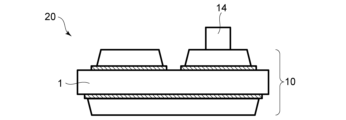
- FIG. 5 is a side view showing an example of a semiconductor device according to an embodiment.
- reference numeral 10 denotes a silicon nitride circuit board
- reference numeral 14 denotes a semiconductor element
- reference numeral 20 denotes a semiconductor device.
- FIG. 5 shows an example in which one semiconductor element 14 is mounted, but multiple semiconductor elements 14 may also be mounted. Also, a lead frame or wire bonding (not shown) may be provided. Sealing with resin may also be performed.
- the manufacturing process for silicon nitride substrates includes the raw material mixing process, molding process, degreasing process, and sintering process.
- raw material powder is prepared by mixing silicon nitride powder, the main component, with sintering aid powder.
- An organic binder is mixed with the raw material powder to prepare a raw material paste. Either direct nitriding powder or powder produced by the imide decomposition method can be used as the silicon nitride powder.
- a silicon nitride sheet body is prepared from the raw material paste. Methods for preparing a silicon nitride sheet body include the doctor blade method, die molding method, and injection molding.
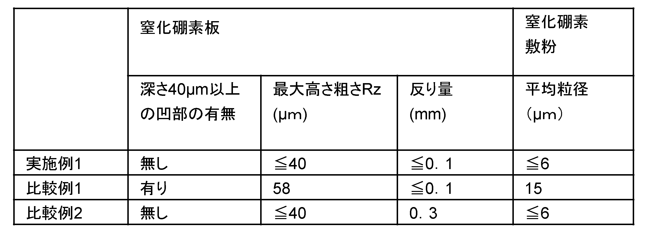
- the degreasing process and the sintering process are preferably performed by placing a sheet-shaped silicon nitride molded body on the boron nitride plate. It is preferable that the surface of the boron nitride plate does not have any recesses with a depth of 40 ⁇ m or more. In addition, it is preferable that the maximum height roughness Rz of the surface of the boron nitride plate is 40 ⁇ m or less. The amount of warping of the boron nitride plate is preferably 0.1 mm or less.
- the warping of the boron nitride plate refers to the greatest distance between the boron nitride plate and a straight line connecting one end of the boron nitride plate and the opposite end of the boron nitride plate. It is preferable that the amount of warping of the boron nitride plate in the long side direction, short side direction, and diagonal direction is 0.2 mm or less.
- the binder is removed from the sheet-shaped silicon nitride molded body.
- the sheet-shaped silicon nitride molded body is called a silicon nitride molded body.
- the silicon nitride molded body is placed on the boron nitride plate.
- a single layer of silicon nitride molded body may be placed, or multiple silicon nitride molded bodies may be stacked.
- a weight plate may be placed on the silicon nitride molded body.
- a layered structure of a boron nitride plate and a silicon nitride molded body may be taken, such as boron nitride plate/silicon nitride molded body/boron nitride plate/silicon nitride molded body.
- a powder may be used between the silicon nitride molded bodies.
- the powder is preferably boron nitride powder with an average particle size of 10 ⁇ m or less.
- a powder with a small particle size can reduce the surface unevenness of the silicon nitride substrate 1. For this reason, the average particle size of the powder is preferably 10 ⁇ m or less, and more preferably 6 ⁇ m or less.
- the effect of suppressing warping of the silicon nitride substrate 1 can be obtained.
- the effect of suppressing warping of the silicon nitride substrate 1 can be obtained.
- the degreasing process is preferably carried out at a temperature in the range of 350°C to 600°C.
- the degreasing process removes the organic binder from the silicon nitride compact.
- the degreasing process produces a silicon nitride degreased body.
- the silicon nitride substrate 1 can be obtained by the above steps. If necessary, steps such as a powder removal step, a cleaning step, and a warping correction step may be performed. The surface of the silicon nitride substrate 1 may be inspected, and only the silicon nitride substrate 1 included in the embodiment may be selected.
- Example 2 (Examples 1 to 7, Comparative Examples 1 to 2) A raw material powder was prepared by mixing silicon nitride powder and a sintering aid. A binder and the like were added to the raw material powder, and a sheet-shaped silicon nitride molded body was produced by the doctor blade method. A boron nitride plate and boron nitride bedding powder were used to carry out a degreasing process and a sintering process for the sheet-shaped silicon nitride molded body. The degreasing process was carried out in the range of 350°C to 600°C. The sintering process was carried out in the range of 1600°C to 2000°C.
- the size of the silicon nitride substrate was 120 mm long x 100 mm wide.
- the boron nitride plate and boron nitride bedding powder used are as shown in Table 1.
- the preferred manufacturing conditions are met.
- the boron nitride plate has little warping, but large irregularities.
- the average particle size of the powder is larger than in the examples.
- the boron nitride plate has little irregularities, but the amount of warping is large.
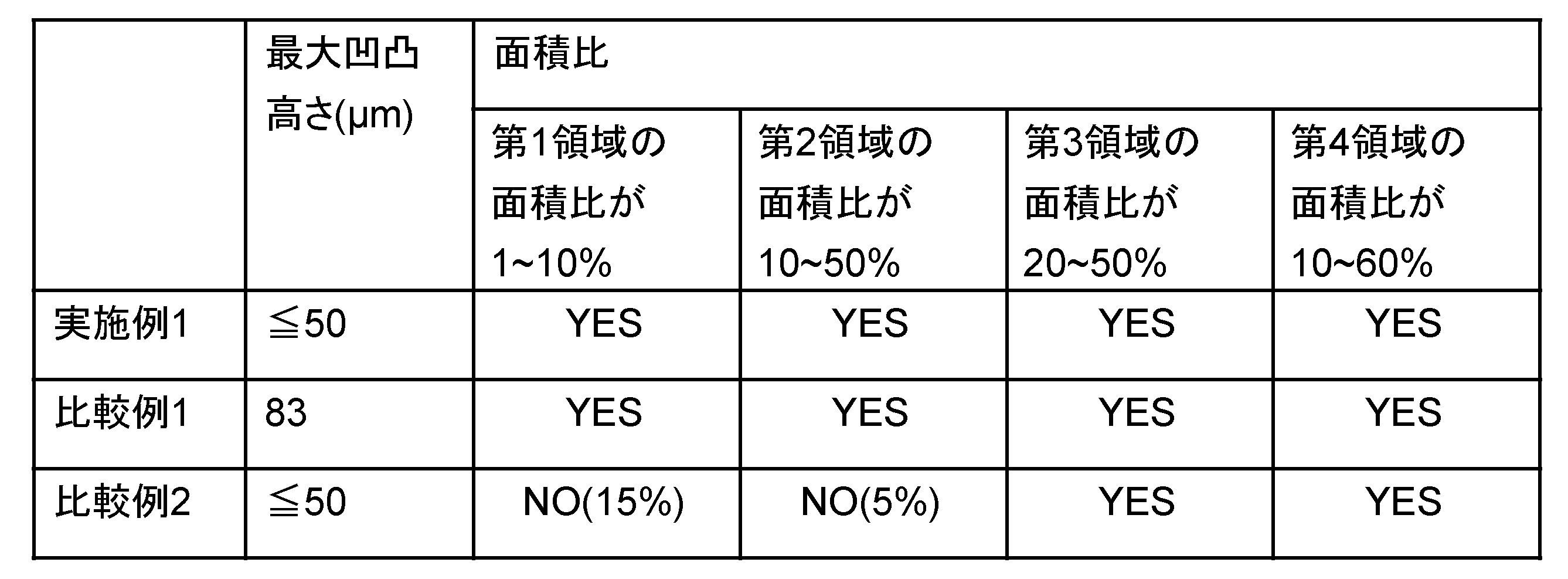
- the surface unevenness of the obtained silicon nitride substrate was inspected. Several 6 mm x 6 mm sections were randomly selected on the surface of the silicon nitride substrate, and the unevenness of each section was observed. A three-dimensional shape measuring device (Keyence VR-3000) was used to observe the unevenness. The method for measuring the maximum unevenness height and the area ratio of the first to fourth regions was as described above. The area ratio of each of the first to fourth regions was calculated assuming that the sum of the areas of the first to fourth regions was 100%. The results are shown in Table 2. In Table 2, “YES” indicates that the area ratio of each region was within the specified range. “NO” indicates that the area ratio of each region was outside the specified range.
- the maximum unevenness height was 50 ⁇ m or less in all 6 mm x 6 mm parts, and the area ratio of each region was within the specified range. In the examples, the preferred conditions for the maximum unevenness height and area ratio were met.
- Example 1 there was a mixture of regions with a maximum unevenness height of 5 ⁇ m or more and 25 ⁇ m or less, and regions with a maximum unevenness height of more than 25 ⁇ m and 50 ⁇ m or less.
- Comparative Example 1 there was a portion with a maximum unevenness height of 83 ⁇ m. That is, in Comparative Example 1, the area ratio of each region was within the specified range, but there was a portion with a maximum unevenness height exceeding 50 ⁇ m.
- Comparative Example 2 the area ratio of the first region was 15%, and the area ratio of the second region was 5%. That is, in Comparative Example 2, the maximum unevenness height was 50 ⁇ m, but there was a portion with the area ratio of the first region and the area ratio of the second region outside the range.
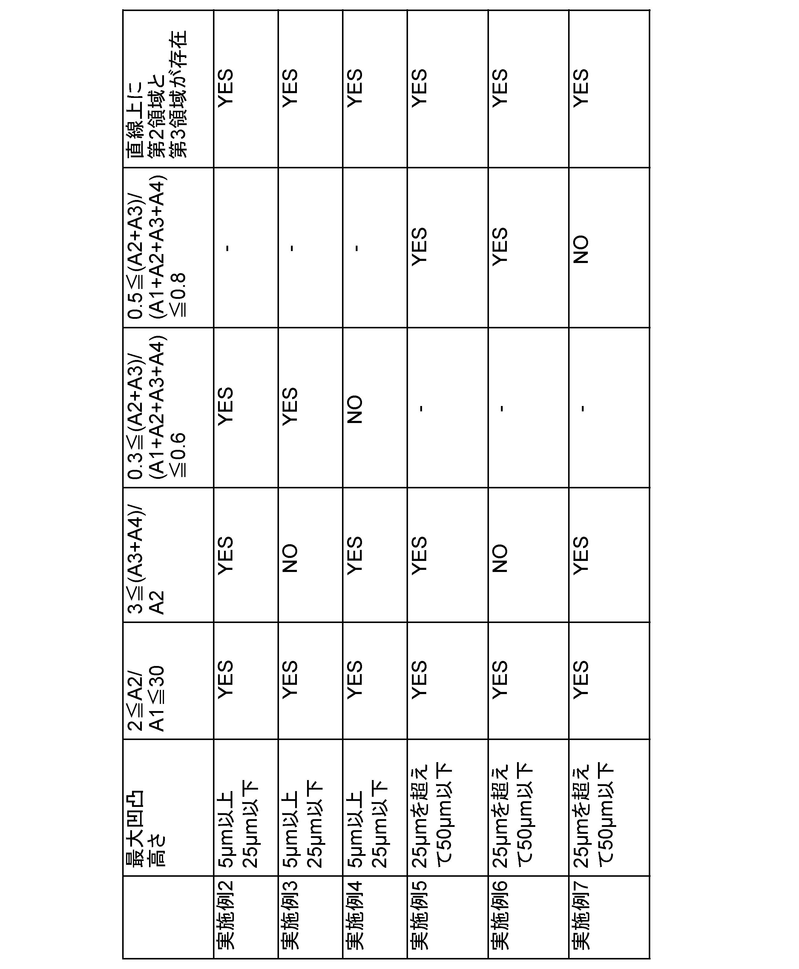
- the silicon nitride substrate of Example 1 was classified according to the relationship of the area ratio of each region. Specifically, the area of the first region 6 is A1, the area of the second region 7 is A2, the area of the third region 8 is A3, and the area of the fourth region 9 is A4. In this case, for each substrate, it was determined whether or not each of the following conditions was satisfied: 2 ⁇ A2/A1 ⁇ 30, 3 ⁇ (A3+A4)/A2, 0.3 ⁇ (A2+A3)/(A1+A2+A3+A4) ⁇ 0.6, and 0.5 ⁇ (A2+A3)/(A1+A2+A3+A4) ⁇ 0.8.
- Example 1 was classified into Examples 2 to 7 according to whether or not each condition was satisfied. The results are shown in Table 3. In Table 3, "YES” indicates that the condition is satisfied, and "NO” indicates that the condition is not satisfied. For the condition 0.3 ⁇ (A2+A3)/(A1+A2+A3+A4) ⁇ 0.6, the evaluation was conducted for Examples 2 to 4, in which the maximum unevenness height was 5 ⁇ m or more and 25 ⁇ m or less. For the condition 0.5 ⁇ (A2+A3)/(A1+A2+A3+A4) ⁇ 0.8, the evaluation was conducted for Examples 5 to 7, in which the maximum unevenness height was more than 25 ⁇ m and 50 ⁇ m or less.
- Table 4 also shows the measurement results of the maximum unevenness height and the area ratio of the first to fourth regions in any 6 mm x 6 mm area for the silicon nitride substrates of Examples 2 to 7.
- metal plates were bonded to the front and back surfaces of the silicon nitride substrate using active metal bonding.
- a 0.8 mm thick copper plate was bonded to the front surface to form a circuit section.
- a 0.8 mm thick copper plate was bonded to the back surface as a heat sink.
- a brazing material containing Ti as an active metal was used for the active metal brazing material.
- the copper plate on the front surface was etched to give it a circuit shape, forming the circuit section. Through these processes, a silicon nitride circuit substrate was produced.
- the silicon nitride circuit boards of the examples and comparative examples were examined for the presence or absence of bonding defects. Bonding defects were examined using ultrasonic testing (SAT). Examples where the area ratio of bonding defects in the circuit section was between 0% and 1% were rated "excellent”. Examples where the area ratio of bonding defects was between 1% and 3% or less were rated "good”. Examples where the area ratio of bonding defects was between 3% and 5% or less were rated "passable”. Examples where the area ratio of bonding defects exceeded 5% were rated "unacceptable”. The area ratio of bonding defects in 10 silicon nitride circuit boards for each example and comparative example was measured, and the result with the largest area ratio of bonding defects was recorded.
- SAT ultrasonic testing
- Embodiments of the invention include the following features.
- (Feature 1) When the unevenness is observed in a 6 mm ⁇ 6 mm area on at least one surface of the silicon nitride substrate, the maximum unevenness height, which is the difference between the height of the maximum convexity and the depth of the maximum concaveity, is 50 ⁇ m or less;
- the portion is A first region having a height ratio to the maximum irregularity height of 0.8 or more and 1.0 or less;
- a second region having a height ratio of 0.5 or more and less than 0.8; a third region having a height ratio of 0.3 or more and less than 0.5;
- Including, a ratio of an area of the first region to a total area of the first to fourth regions is 1% or more and 10% or less; a ratio of an area of the second region to the total area is 10% or more and 50% or less; a ratio of an area of the third region to the total area is
- (Feature 2) 2. The silicon nitride substrate according to claim 1, wherein the ratio of the area of the second region to the area of the first region is 2.ltoreq.30. (Feature 3) 3 ⁇ (the area of the third region+the area of the fourth region)/the area of the second region. (Feature 4) The maximum unevenness height is 5 ⁇ m or more and 25 ⁇ m or less, 4. The silicon nitride substrate according to any one of features 1 to 3, wherein 0.3 ⁇ (the area of the second region+the area of the third region)/the total area ⁇ 0.6 is satisfied. (Feature 5) The maximum irregularity height is more than 25 ⁇ m and not more than 50 ⁇ m, 4.
- (Feature 6) 6.
- feature 7) 7.
- (Feature 8) 8.
- a silicon nitride circuit board comprising:
Landscapes
- Engineering & Computer Science (AREA)
- Microelectronics & Electronic Packaging (AREA)
- Manufacturing & Machinery (AREA)
- Chemical & Material Sciences (AREA)
- Ceramic Engineering (AREA)
- Inorganic Chemistry (AREA)
- Ceramic Products (AREA)
Abstract
Description
(実施例1~7、比較例1~2)
窒化珪素粉と焼結助剤を混合した原料粉末を用意した。原料粉末にバインダなどを添加し、ドクターブレード法により、シート状窒化珪素成形体を作製した。窒化硼素板、窒化硼素敷粉を用いて、シート状窒化珪素成形体の脱脂工程および焼結工程を行った。脱脂工程は、350℃以上600℃以下の範囲内で行った。焼結工程は、1600℃以上2000℃以下の範囲内で行った。これにより、窒化珪素基板を得た。窒化珪素基板のサイズは、縦120mm×横100mmである。使用した窒化硼素板および窒化硼素敷粉は、表1に示した通りである。


(特徴1)
窒化珪素基板の少なくとも一方の面における6mm×6mmの部分の凹凸を観察した場合に、最大凸部の高さと最大凹部の深さとの差である最大凹凸高さが50μm以下であり、
前記部分は、
前記最大凹凸高さに対する高さ比が0.8以上1.0以下の第1領域と、
前記高さ比が0.5以上0.8未満の第2領域と、
前記高さ比が0.3以上0.5未満の第3領域と、
前記高さ比が0以上0.3未満の第4領域と、
を含み、
前記第1乃至前記第4領域の合計面積に対する前記第1領域の面積の比は、1%以上10%以下であり、
前記合計面積に対する前記第2領域の面積の比は、10%以上50%以下であり、
前記合計面積に対する前記第3領域の面積の比は、20%以上50%以下であり、
前記合計面積に対する前記第4領域の面積の比は、10%以上60%以下である、窒化珪素基板。
(特徴2)
2≦前記第2領域の前記面積/前記第1領域の前記面積≦30、を満たす特徴1記載の窒化珪素基板。
(特徴3)
3≦(前記第3領域の前記面積+前記第4領域の前記面積)/前記第2領域の前記面積、を満たす特徴1または特徴2に記載の窒化珪素基板。
(特徴4)
前記最大凹凸高さが5μm以上25μm以下であり、
0.3≦(前記第2領域の前記面積+前記第3領域の前記面積)/前記合計面積≦0.6、を満たす特徴1乃至特徴3のいずれか1つに記載の窒化珪素基板。
(特徴5)
前記最大凹凸高さが25μmを超えて50μm以下であり、
0.5≦(前記第2領域の前記面積+前記第3領域の前記面積)/前記合計面積≦0.8、を満たす特徴1乃至特徴3のいずれか1つに記載の窒化珪素基板。
(特徴6)
前記部分において、前記最大凸部と前記最大凹部とを直線で結んだ場合に、前記直線上に前記第2領域と前記第3領域の両方が存在している、特徴1乃至特徴5のいずれか1つに記載の窒化珪素基板。
(特徴7)
基板厚さが0.2mm以上3mm以下である、特徴1乃至特徴6のいずれか1つに記載の窒化珪素基板。
(特徴8)
縦の寸法が50mm以上であり、横の寸法が50mm以上である特徴7に記載の窒化珪素基板。
(特徴9)
特徴1乃至特徴8のいずれか1つに記載の前記窒化珪素基板と、
前記窒化珪素基板の上に設けられた回路部と、
を備えた窒化珪素回路基板。
2…面
3…最大凸部
4…最大凹部
5…最大凹凸高さ
6…第1領域
7…第2領域
8…第3領域
9…第4領域
10…窒化珪素回路基板
11…回路部
12…接合層
13…放熱部
14…半導体素子
20…半導体装置
Claims (19)
- 窒化珪素基板の少なくとも一方の面における6mm×6mmの部分の凹凸を観察した場合に、最大凸部の高さと最大凹部の深さとの差である最大凹凸高さが50μm以下であり、
前記部分は、
前記最大凹凸高さに対する高さ比が0.8以上1.0以下の第1領域と、
前記高さ比が0.5以上0.8未満の第2領域と、
前記高さ比が0.3以上0.5未満の第3領域と、
前記高さ比が0以上0.3未満の第4領域と、
を含み、
前記第1乃至前記第4領域の合計面積に対する前記第1領域の面積の比は、1%以上10%以下であり、
前記合計面積に対する前記第2領域の面積の比は、10%以上50%以下であり、
前記合計面積に対する前記第3領域の面積の比は、20%以上50%以下であり、
前記合計面積に対する前記第4領域の面積の比は、10%以上60%以下である、窒化珪素基板。 - 2≦前記第2領域の前記面積/前記第1領域の前記面積≦30、を満たす請求項1記載の窒化珪素基板。
- 3≦(前記第3領域の前記面積+前記第4領域の前記面積)/前記第2領域の前記面積、を満たす請求項1または請求項2に記載の窒化珪素基板。
- 前記最大凹凸高さが5μm以上25μm以下であり、
0.3≦(前記第2領域の前記面積+前記第3領域の前記面積)/前記合計面積≦0.6、を満たす請求項1または請求項2に記載の窒化珪素基板。 - 前記最大凹凸高さが5μm以上25μm以下であり、
0.3≦(前記第2領域の前記面積+前記第3領域の前記面積)/前記合計面積≦0.6、を満たす請求項3に記載の窒化珪素基板。 - 前記最大凹凸高さが25μmを超えて50μm以下であり、
0.5≦(前記第2領域の前記面積+前記第3領域の前記面積)/前記合計面積≦0.8、を満たす請求項1または請求項2に記載の窒化珪素基板。 - 前記最大凹凸高さが25μmを超えて50μm以下であり、
0.5≦(前記第2領域の前記面積+前記第3領域の前記面積)/前記合計面積≦0.8、を満たす請求項3に記載の窒化珪素基板。 - 前記部分において、前記最大凸部と前記最大凹部とを直線で結んだ場合に、前記直線上に前記第2領域と前記第3領域の両方が存在している、請求項1または請求項2に記載の窒化珪素基板。
- 前記部分において、前記最大凸部と前記最大凹部とを直線で結んだ場合に、前記直線上に前記第2領域と前記第3領域の両方が存在している、請求項5に記載の窒化珪素基板。
- 前記部分において、前記最大凸部と前記最大凹部とを直線で結んだ場合に、前記直線上に前記第2領域と前記第3領域の両方が存在している、請求項7に記載の窒化珪素基板。
- 基板厚さが0.2mm以上3mm以下である、請求項1または請求項2に記載の窒化珪素基板。
- 基板厚さが0.2mm以上3mm以下である、請求項5に記載の窒化珪素基板。
- 基板厚さが0.2mm以上3mm以下である、請求項8に記載の窒化珪素基板。
- 縦の寸法が50mm以上であり、横の寸法が50mm以上である請求項11に記載の窒化珪素基板。
- 縦の寸法が50mm以上であり、横の寸法が50mm以上である請求項12に記載の窒化珪素基板。
- 縦の寸法が50mm以上であり、横の寸法が50mm以上である請求項13に記載の窒化珪素基板。
- 請求項1または請求項2に記載の前記窒化珪素基板と、
前記窒化珪素基板の上に設けられた回路部と、
を備えた窒化珪素回路基板。 - 請求項12に記載の前記窒化珪素基板と、
前記窒化珪素基板の上に設けられた回路部と、
を備えた窒化珪素回路基板。 - 請求項13に記載の前記窒化珪素基板と、
前記窒化珪素基板の上に設けられた回路部と、
を備えた窒化珪素回路基板。
Priority Applications (3)
| Application Number | Priority Date | Filing Date | Title |
|---|---|---|---|
| EP24744747.7A EP4654258A1 (en) | 2023-01-20 | 2024-01-19 | Silicon nitride substrate and silicon nitride circuit board using same |
| CN202480004763.5A CN120188275A (zh) | 2023-01-20 | 2024-01-19 | 氮化硅基板及使用其的氮化硅电路基板 |
| JP2024571811A JP7810829B2 (ja) | 2023-01-20 | 2024-01-19 | 窒化珪素基板およびそれを用いた窒化珪素回路基板 |
Applications Claiming Priority (2)
| Application Number | Priority Date | Filing Date | Title |
|---|---|---|---|
| JP2023007022 | 2023-01-20 | ||
| JP2023-007022 | 2023-01-20 |
Publications (1)
| Publication Number | Publication Date |
|---|---|
| WO2024154827A1 true WO2024154827A1 (ja) | 2024-07-25 |
Family
ID=91955943
Family Applications (1)
| Application Number | Title | Priority Date | Filing Date |
|---|---|---|---|
| PCT/JP2024/001489 Ceased WO2024154827A1 (ja) | 2023-01-20 | 2024-01-19 | 窒化珪素基板およびそれを用いた窒化珪素回路基板 |
Country Status (4)
| Country | Link |
|---|---|
| EP (1) | EP4654258A1 (ja) |
| JP (1) | JP7810829B2 (ja) |
| CN (1) | CN120188275A (ja) |
| WO (1) | WO2024154827A1 (ja) |
Citations (6)
| Publication number | Priority date | Publication date | Assignee | Title |
|---|---|---|---|---|
| JP3539634B2 (ja) | 2000-10-26 | 2004-07-07 | 日立金属株式会社 | 回路搭載用窒化ケイ素基板および回路基板 |
| JP2014127503A (ja) * | 2012-12-25 | 2014-07-07 | Kyocera Corp | 配線基板および電子装置 |
| JP6293772B2 (ja) | 2013-10-23 | 2018-03-14 | 株式会社東芝 | 窒化珪素基板およびそれを用いた窒化珪素回路基板 |
| WO2018173921A1 (ja) * | 2017-03-23 | 2018-09-27 | 株式会社 東芝 | セラミックス金属回路基板およびそれを用いた半導体装置 |
| JP6789955B2 (ja) | 2015-09-28 | 2020-11-25 | 株式会社東芝 | 回路基板および半導体装置 |
| WO2021095845A1 (ja) * | 2019-11-15 | 2021-05-20 | デンカ株式会社 | セラミック基板、複合基板及び回路基板並びにセラミック基板の製造方法、複合基板の製造方法、回路基板の製造方法及び複数の回路基板の製造方法 |
-
2024
- 2024-01-19 EP EP24744747.7A patent/EP4654258A1/en active Pending
- 2024-01-19 JP JP2024571811A patent/JP7810829B2/ja active Active
- 2024-01-19 CN CN202480004763.5A patent/CN120188275A/zh active Pending
- 2024-01-19 WO PCT/JP2024/001489 patent/WO2024154827A1/ja not_active Ceased
Patent Citations (6)
| Publication number | Priority date | Publication date | Assignee | Title |
|---|---|---|---|---|
| JP3539634B2 (ja) | 2000-10-26 | 2004-07-07 | 日立金属株式会社 | 回路搭載用窒化ケイ素基板および回路基板 |
| JP2014127503A (ja) * | 2012-12-25 | 2014-07-07 | Kyocera Corp | 配線基板および電子装置 |
| JP6293772B2 (ja) | 2013-10-23 | 2018-03-14 | 株式会社東芝 | 窒化珪素基板およびそれを用いた窒化珪素回路基板 |
| JP6789955B2 (ja) | 2015-09-28 | 2020-11-25 | 株式会社東芝 | 回路基板および半導体装置 |
| WO2018173921A1 (ja) * | 2017-03-23 | 2018-09-27 | 株式会社 東芝 | セラミックス金属回路基板およびそれを用いた半導体装置 |
| WO2021095845A1 (ja) * | 2019-11-15 | 2021-05-20 | デンカ株式会社 | セラミック基板、複合基板及び回路基板並びにセラミック基板の製造方法、複合基板の製造方法、回路基板の製造方法及び複数の回路基板の製造方法 |
Non-Patent Citations (1)
| Title |
|---|
| See also references of EP4654258A1 |
Also Published As
| Publication number | Publication date |
|---|---|
| EP4654258A1 (en) | 2025-11-26 |
| JP7810829B2 (ja) | 2026-02-03 |
| JPWO2024154827A1 (ja) | 2024-07-25 |
| CN120188275A (zh) | 2025-06-20 |
Similar Documents
| Publication | Publication Date | Title |
|---|---|---|
| JP6750404B2 (ja) | 熱電変換モジュール及び熱電変換装置並びに熱電変換モジュールの製造方法 | |
| JP4241397B2 (ja) | 回路基板の製造方法 | |
| JP7163631B2 (ja) | 熱電変換モジュール、及び、熱電変換モジュールの製造方法 | |
| CN110383468A (zh) | 带散热片的功率模块用基板 | |
| WO2020162445A1 (ja) | 銅/セラミックス接合体の製造方法、絶縁回路基板の製造方法、銅/セラミックス接合体、及び、絶縁回路基板 | |
| JPWO2019221174A1 (ja) | セラミックス銅回路基板およびその製造方法 | |
| WO2013122126A1 (ja) | はんだ接合構造、パワーモジュール、ヒートシンク付パワーモジュール用基板及びそれらの製造方法、並びにはんだ下地層形成用ペースト | |
| CN101529588A (zh) | 功率模块用基板以及功率模块用基板的制造方法、及功率模块 | |
| JP6638284B2 (ja) | 放熱板付パワーモジュール用基板及びパワーモジュール | |
| JP6656657B2 (ja) | セラミックス/アルミニウム接合体、パワーモジュール用基板、及び、パワーモジュール | |
| EP3093882A1 (en) | Electronic circuit device | |
| WO2020208698A1 (ja) | 接合基板及び接合基板の製造方法 | |
| JP7197677B2 (ja) | 接合基板 | |
| JP2021132238A (ja) | 回路基板および半導体モジュール | |
| WO2023008562A1 (ja) | 銅/セラミックス接合体、および、絶縁回路基板 | |
| TWI726048B (zh) | 附有銀基材層之金屬構件、附有銀基材層之絕緣電路基板、半導體裝置、附有散熱片之絕緣電路基板及附有銀基材層之金屬構件之製造方法 | |
| CN108028306A (zh) | 热电转换模块及热电转换装置 | |
| JP7810829B2 (ja) | 窒化珪素基板およびそれを用いた窒化珪素回路基板 | |
| JP5966504B2 (ja) | はんだ接合構造、パワーモジュール、ヒートシンク付パワーモジュール用基板、並びに、はんだ接合構造の製造方法、パワーモジュールの製造方法、ヒートシンク付パワーモジュール用基板の製造方法 | |
| WO2016052392A1 (ja) | Ag下地層付パワーモジュール用基板及びパワーモジュール | |
| JP4772187B2 (ja) | AlN焼結体およびこれを用いたAlN回路基板 | |
| KR102529238B1 (ko) | 세라믹 기판 및 이의 제조방법 | |
| TW202242910A (zh) | 接合構造體 | |
| WO2025134898A1 (ja) | セラミックス回路基板及びその製造方法 | |
| JP2017188675A (ja) | 放熱基板 |
Legal Events
| Date | Code | Title | Description |
|---|---|---|---|
| 121 | Ep: the epo has been informed by wipo that ep was designated in this application |
Ref document number: 24744747 Country of ref document: EP Kind code of ref document: A1 |
|
| WWE | Wipo information: entry into national phase |
Ref document number: 2024571811 Country of ref document: JP |
|
| WWE | Wipo information: entry into national phase |
Ref document number: 202480004763.5 Country of ref document: CN |
|
| WWP | Wipo information: published in national office |
Ref document number: 202480004763.5 Country of ref document: CN |
|
| NENP | Non-entry into the national phase |
Ref country code: DE |
|
| WWP | Wipo information: published in national office |
Ref document number: 2024744747 Country of ref document: EP |