WO2024185152A1 - 放射線検出装置、その製造方法及び放射線ct装置 - Google Patents
放射線検出装置、その製造方法及び放射線ct装置 Download PDFInfo
- Publication number
- WO2024185152A1 WO2024185152A1 PCT/JP2023/010822 JP2023010822W WO2024185152A1 WO 2024185152 A1 WO2024185152 A1 WO 2024185152A1 JP 2023010822 W JP2023010822 W JP 2023010822W WO 2024185152 A1 WO2024185152 A1 WO 2024185152A1
- Authority
- WO
- WIPO (PCT)
- Prior art keywords
- semiconductor layer
- detection device
- radiation detection
- electrode
- substrate
- Prior art date
- Legal status (The legal status is an assumption and is not a legal conclusion. Google has not performed a legal analysis and makes no representation as to the accuracy of the status listed.)
- Ceased
Links
Images
Classifications
-
- H—ELECTRICITY
- H10—SEMICONDUCTOR DEVICES; ELECTRIC SOLID-STATE DEVICES NOT OTHERWISE PROVIDED FOR
- H10F—INORGANIC SEMICONDUCTOR DEVICES SENSITIVE TO INFRARED RADIATION, LIGHT, ELECTROMAGNETIC RADIATION OF SHORTER WAVELENGTH OR CORPUSCULAR RADIATION
- H10F39/00—Integrated devices, or assemblies of multiple devices, comprising at least one element covered by group H10F30/00, e.g. radiation detectors comprising photodiode arrays
- H10F39/10—Integrated devices
- H10F39/12—Image sensors
- H10F39/18—Complementary metal-oxide-semiconductor [CMOS] image sensors; Photodiode array image sensors
- H10F39/189—X-ray, gamma-ray or corpuscular radiation imagers
- H10F39/1895—X-ray, gamma-ray or corpuscular radiation imagers of the hybrid type
-
- G—PHYSICS
- G01—MEASURING; TESTING
- G01T—MEASUREMENT OF NUCLEAR OR X-RADIATION
- G01T1/00—Measuring X-radiation, gamma radiation, corpuscular radiation, or cosmic radiation
- G01T1/16—Measuring radiation intensity
- G01T1/24—Measuring radiation intensity with semiconductor detectors
- G01T1/244—Auxiliary details, e.g. casings, cooling, damping or insulation against damage by, e.g. heat, pressure or the like
-
- G—PHYSICS
- G01—MEASURING; TESTING
- G01T—MEASUREMENT OF NUCLEAR OR X-RADIATION
- G01T1/00—Measuring X-radiation, gamma radiation, corpuscular radiation, or cosmic radiation
- G01T1/16—Measuring radiation intensity
- G01T1/24—Measuring radiation intensity with semiconductor detectors
- G01T1/241—Electrode arrangements, e.g. continuous or parallel strips or the like
-
- H—ELECTRICITY
- H10—SEMICONDUCTOR DEVICES; ELECTRIC SOLID-STATE DEVICES NOT OTHERWISE PROVIDED FOR
- H10F—INORGANIC SEMICONDUCTOR DEVICES SENSITIVE TO INFRARED RADIATION, LIGHT, ELECTROMAGNETIC RADIATION OF SHORTER WAVELENGTH OR CORPUSCULAR RADIATION
- H10F39/00—Integrated devices, or assemblies of multiple devices, comprising at least one element covered by group H10F30/00, e.g. radiation detectors comprising photodiode arrays
- H10F39/80—Constructional details of image sensors
- H10F39/811—Interconnections
Definitions
- the present invention relates to a radiation detection device, its manufacturing method, and a radiation CT device.
- Patent Document 1 proposes improving the moisture resistance of a semiconductor layer in a radiation detection device that directly converts radiation into an electric charge in a semiconductor layer by covering the side surfaces of the semiconductor layer with an organic layer.
- a radiation detection device includes a substrate, a first electrode located on the substrate, a semiconductor layer located on the first electrode, the semiconductor layer generating charges according to radiation incident on the radiation detection device, a second electrode located on the semiconductor layer and having a first surface in contact with the semiconductor layer and a second surface opposite to the first surface, and an insulating layer in contact with the second surface of the second electrode.
- the detection portion of the radiation detection device is appropriately protected.
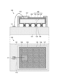
- FIG. 1 is a schematic diagram illustrating an example of the configuration of a radiation detection device according to some embodiments.
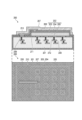
- FIG. 1 is a schematic diagram illustrating an example of the configuration of a radiation detection device according to some embodiments.
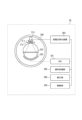
- FIG. 1 is a block diagram illustrating an example of the configuration of a radiation CT apparatus according to some embodiments.
- the radiation detection device 100 has a function of detecting incident radiation.
- the radiation detection device 100 may be called a radiation imaging device.
- the upper diagram of FIG. 1 shows a side cross-sectional view of the radiation detection device 100.
- the lower diagram of FIG. 1 shows a plan view of the radiation detection device 100. In the plan view, the outlines of components hidden by other components are shown with dashed lines.
- the sealing member 107 is omitted and its outline is shown with dashed lines to make the arrangement of the insulating layer 106 easier to understand.
- the radiation detection device 100 has a substrate 101 and a detection unit 102 located on the substrate 101.
- the surface of the substrate 101 on which the detection unit 102 is located is called the top surface (the upper surface in the side cross-sectional view).
- the surface of the substrate 101 opposite the top surface is called the bottom surface (the lower surface in the side cross-sectional view).
- the surfaces of the substrate 101 connecting the top surface and bottom surface are called side surfaces (the left and right surfaces in the side cross-sectional view).
- the substrate 101 has four side surfaces.
- the substrate 101 may be, for example, a printed circuit board (which may also be called a printed circuit board).
- the detection unit 102 has an upper electrode 103, a semiconductor layer 104, and a lower electrode 105.
- the semiconductor layer 104 is sandwiched between the upper electrode 103 and the lower electrode 105.
- the lower electrode 105 is located on the substrate 101
- the semiconductor layer 104 is located on the lower electrode 105
- the upper electrode 103 is located on the semiconductor layer 104.
- the radiation detection device 100 has an individual lower electrode 105 for each pixel.
- the radiation detection device 100 has pixels arranged in 4 rows and 4 columns. Therefore, the radiation detection device 100 has a total of 16 lower electrodes 105 arranged in 4 rows and 4 columns.
- the number of pixels that the radiation detection device 100 has is not limited to this example, and the radiation detection device 100 typically has more pixels.
- the upper electrode 103 is commonly arranged across multiple pixels. In the example of FIG. 1, the radiation detection device 100 has one common upper electrode 103 for 16 pixels. Alternatively, the radiation detection device 100 may have an individual (i.e., a total of 16) upper electrodes 103 for each pixel.
- the surface of the semiconductor layer 104 on which the upper electrode 103 is disposed is called the top surface (the upper surface in the side cross-sectional view).
- the surface of the semiconductor layer 104 opposite the top surface is called the bottom surface (the lower surface in the side cross-sectional view).
- the surfaces of the semiconductor layer 104 connecting the top surface and bottom surface are called the side surfaces (the left and right surfaces in the side cross-sectional view).
- the semiconductor layer 104 has a rectangular parallelepiped shape, the semiconductor layer 104 has four side surfaces facing in different directions.
- the surface of the upper electrode 103 on which the semiconductor layer 104 is disposed is called the bottom surface (the bottom surface in the side cross-sectional view).
- the surface of the upper electrode 103 opposite the bottom surface is called the top surface (the top surface in the side cross-sectional view).
- the surfaces of the upper electrode 103 connecting the top and bottom surfaces are called the side surfaces (the left and right surfaces in the side cross-sectional view).
- the upper electrode 103 has a rectangular parallelepiped shape, the upper electrode 103 has four side surfaces facing in different directions.
- the surface of the lower electrode 105 on which the semiconductor layer 104 is disposed is called the top surface (the upper surface in the side cross-sectional view).
- the surface of the lower electrode 105 opposite the top surface is called the bottom surface (the lower surface in the side cross-sectional view).
- the surfaces of the lower electrode 105 connecting the top and bottom surfaces are called the side surfaces (the left and right surfaces in the side cross-sectional view).
- the lower electrode 105 has a rectangular parallelepiped shape, the lower electrode 105 has four side surfaces facing in different directions. As shown in FIG. 1, the side surfaces of the lower electrode 105 have steps.
- the lower surface of the upper electrode 103 is in contact with the upper surface of the semiconductor layer 104.
- the upper surface of the semiconductor layer 104 has the same shape as the lower surface of the upper electrode 103.
- the outer edge of the upper surface of the semiconductor layer 104 coincides with the outer edge of the lower surface of the upper electrode 103. Therefore, the entire lower surface of the upper electrode 103 is in contact with the entire upper surface of the semiconductor layer 104.
- the lower surface of the upper electrode 103 may be smaller than the upper surface of the semiconductor layer 104.
- the upper electrode 103 may extend to the side surface of the semiconductor layer 104 and be in contact with at least a portion of the side surface of the semiconductor layer 104.
- the upper surface of the lower electrode 105 is in contact with the lower surface of the semiconductor layer 104.
- the upper surface of the lower electrode 105 is smaller than the lower surface of the semiconductor layer 104. Therefore, the entire upper surface of the lower electrode 105 is in contact with a portion of the lower surface of the semiconductor layer 104.
- the semiconductor layer 104 generates charges in response to radiation incident on the radiation detection device 100.
- the semiconductor layer 104 may generate charges in response to radiation incident on the semiconductor layer 104.
- the semiconductor layer 104 may be composed of a compound semiconductor such as cadmium zinc telluride.
- the upper electrode 103 and the lower electrode 105 are each made of a conductor.
- the upper electrode 103 and the lower electrode 105 may each be made of a metal such as copper.
- At least a portion of the detection unit 102 is covered by an insulating layer 106.
- the specific arrangement of the insulating layer 106 is described below.
- the insulating layer 106 covers a portion of the upper surface of the upper electrode 103.
- the portion of the insulating layer 106 that covers a portion of the upper surface of the upper electrode 103 is in contact with the upper surface of the upper electrode 103.
- the portion of the upper surface of the upper electrode 103 that is not covered by the insulating layer 106 is used to connect the wire 110.
- the insulating layer 106 includes a portion that covers the side surfaces of the upper electrode 103.
- the portion of the insulating layer 106 that covers the side surfaces of the upper electrode 103 is in contact with the side surfaces of the upper electrode 103.
- the insulating layer 106 covers all four side surfaces of the upper electrode 103.
- the insulating layer 106 may cover only some of the four side surfaces of the upper electrode 103.
- the insulating layer 106 includes a portion that covers the side surfaces of the semiconductor layer 104.
- the portion of the insulating layer 106 that covers the side surfaces of the semiconductor layer 104 is in contact with the side surfaces of the semiconductor layer 104.
- the insulating layer 106 covers all four side surfaces of the semiconductor layer 104.
- the insulating layer 106 may cover only some of the four side surfaces of the semiconductor layer 104.
- the insulating layer 106 includes a portion that covers part of the lower surface of the semiconductor layer 104.
- the portion of the insulating layer 106 that covers part of the lower surface of the semiconductor layer 104 contacts the lower surface of the semiconductor layer 104.
- the insulating layer 106 contacts the entire portion of the lower surface of the semiconductor layer 104 that is not in contact with the lower electrode 105.
- the insulating layer 106 extends from above the detection unit 102 to the side of the detection unit 102, and further extends below the detection unit 102.
- the insulating layer 106 may be made of, for example, an inorganic material. Specifically, the insulating layer 106 may be made of an oxide, a nitride, or an oxynitride. More specifically, the insulating layer 106 may be made of silicon nitride, silicon oxide, silicon oxynitride, or aluminum oxide. The insulating layer 106 may be made of a single layer, or may be made of a laminate including multiple layers. When the insulating layer 106 is made of a laminate, each of the multiple layers may be made of the same material or may be made of different materials. The insulating layer 106 may be made of, for example, an organic material. Furthermore, the insulating layer 106 may be a laminate of an inorganic material and an organic material.
- the part of the detection unit 102 can be isolated from the outside world (e.g., the air inside the housing of the radiation detection device 100). This makes it possible to suppress deterioration of the detection unit 102 due to the influence of the outside world.
- the insulating layer 106 since the insulating layer 106 protects the detection unit 102 from the outside world, the insulating layer 106 may be called a protective layer or an insulating protective layer.
- An electrode 109 and an electrode 111 are formed on the upper surface of the substrate 101.
- the lower electrode 105 (specifically, its lower surface) is coupled to the substrate 101 (specifically, its electrode 109) by a bump 108. Since the bump 108 is conductive, the electrode 109 and the lower electrode 105 are electrically connected to each other.
- the bump 108 is formed of, for example, solder.
- the electrode 109 is electrically connected to another circuit mounted on the substrate 101 or another circuit mounted on a substrate different from the substrate 101 through a wiring formed on the substrate 101. When the radiation detection device 100 is in use, a signal corresponding to the charge generated in the semiconductor layer 104 is transmitted to the other circuit through this wiring.
- One end of the wire 110 is connected to the electrode 111 of the substrate 101.
- the other end of the wire 110 is connected to the upper electrode 103 (specifically, its upper surface).
- the electrode 111 and the upper electrode 103 are electrically connected to each other through the wire 110.
- the electrode 111 is electrically connected to another circuit mounted on the substrate 101 or another circuit mounted on a substrate different from the substrate 101 through wiring formed on the substrate 101.
- a predetermined potential is supplied to the upper electrode 103 from the other circuit.
- the sealing member 107 seals the portion of the upper surface of the upper electrode 103 that is not covered by the insulating layer 106. Furthermore, the sealing member 107 extends from a portion on the side of the semiconductor layer 104 to the upper surface of the substrate 101, thereby sealing the space between the detection unit 102 and the substrate 101. In the example of FIG. 1, there is a space (in other words, a region where no solid exists) between the detection unit 102 and the substrate 101. Alternatively, the space between the detection unit 102 and the substrate 101 may be filled with the sealing member 107.
- the sealing member 107 is made of, for example, an organic material.
- the insulating layer 106 covers the upper, side, and lower sides of the detection unit 102.
- the insulating layer 106 may cover only a portion of the upper, side, and lower sides of the detection unit 102, for example, only the upper side, only the side, only the lower side, or the rest of the detection unit 102, other than the upper side, other than the side, and other than the lower side.
- the portions covered by the insulating layer 106 are protected from the outside world.
- the method of manufacturing the radiation detection device 100 will be described.
- the upper electrode 103 is formed on one side of the semiconductor layer 104.
- the semiconductor layer 104 and the upper electrode 103 are then covered with an insulating layer 106, and a portion of this is removed.
- the lower electrode 105 is then formed on the lower surface of the semiconductor layer 104 in the portion where the insulating layer 106 has been removed.
- the lower electrode 105 is then bonded to the electrode 109 of the substrate 101 by a bump 108.
- the portion of the upper electrode 103 of the semiconductor layer 104 that is not covered with the insulating layer 106 is then connected to the electrode 111 of the substrate 101 by a wire 110.
- the detection unit 102 is then sealed with a sealing member 107.
- the radiation detection device 200 has a function of detecting incident radiation.
- the radiation detection device 200 may be called a radiation imaging device.
- the upper diagram in FIG. 2 shows a side cross-sectional view of the radiation detection device 200.
- the lower diagram in FIG. 2 shows a plan view of the radiation detection device 200. In the plan view, the outlines of components hidden by other components are shown with dashed lines.
- the sealing member 207 is omitted and its outline is shown with dashed lines to make the arrangement of the insulating layer 106 easier to understand.
- the radiation detection device 200 has a substrate 201 and a detection unit 202 located on the substrate 201.
- the surface of the substrate 201 on which the detection unit 202 is located is called the top surface (the upper surface in the side cross-sectional view).
- the surface of the substrate 201 opposite the top surface is called the bottom surface (the lower surface in the side cross-sectional view).
- the surfaces of the substrate 201 connecting the top surface and bottom surface are called side surfaces (the left and right surfaces in the side cross-sectional view).
- the substrate 201 has four side surfaces.
- the substrate 201 may be, for example, a semiconductor substrate.
- the detection unit 202 has an upper electrode 203, a semiconductor layer 204, and a lower electrode 205.
- the semiconductor layer 204 is sandwiched between the upper electrode 203 and the lower electrode 205.
- the lower electrode 205 is located on the substrate 201
- the semiconductor layer 204 is located on the lower electrode 205
- the upper electrode 203 is located on the semiconductor layer 204.
- the radiation detection device 200 has an individual lower electrode 205 for each pixel.
- the radiation detection device 200 has pixels arranged in four rows and four columns. Therefore, the radiation detection device 200 has a total of 16 lower electrodes 205 arranged in four rows and four columns.
- the number of pixels that the radiation detection device 200 has is not limited to this example, and the radiation detection device 200 typically has more pixels.
- the upper electrode 203 is commonly arranged across multiple pixels. In the example of FIG. 2, the radiation detection device 200 has one common upper electrode 203 for 16 pixels. Alternatively, the radiation detection device 200 may have an individual (i.e., a total of 16) upper electrodes 203 for each pixel.
- the surface of the semiconductor layer 204 on which the upper electrode 203 is disposed is called the top surface (the upper surface in the side cross-sectional view).
- the surface of the semiconductor layer 204 opposite the top surface is called the bottom surface (the lower surface in the side cross-sectional view).
- the surfaces of the semiconductor layer 204 connecting the top and bottom surfaces are called the side surfaces (the left and right surfaces in the side cross-sectional view).
- the semiconductor layer 204 has a rectangular parallelepiped shape, the semiconductor layer 204 has four side surfaces facing in different directions.
- the surface of the upper electrode 203 on which the semiconductor layer 204 is disposed is called the bottom surface (the bottom surface in the side cross-sectional view).
- the surface of the upper electrode 203 opposite the bottom surface is called the top surface (the top surface in the side cross-sectional view).
- the surfaces of the upper electrode 203 connecting the top and bottom surfaces are called the side surfaces (the left and right surfaces in the side cross-sectional view).
- the upper electrode 203 has a rectangular parallelepiped shape, the upper electrode 203 has four side surfaces facing in different directions.
- the surface of the lower electrode 205 on which the semiconductor layer 204 is disposed is called the top surface (the upper surface in the side cross-sectional view).
- the surface of the lower electrode 205 opposite the top surface is called the bottom surface (the lower surface in the side cross-sectional view).
- the surfaces of the lower electrode 205 connecting the top and bottom surfaces are called the side surfaces (the left and right surfaces in the side cross-sectional view).
- the lower electrode 205 has a rectangular parallelepiped shape, the lower electrode 205 has four side surfaces facing in different directions.
- the lower surface of the upper electrode 203 is in contact with the upper surface of the semiconductor layer 204.
- the upper surface of the semiconductor layer 204 has the same shape as the lower surface of the upper electrode 203.
- the outer edge of the upper surface of the semiconductor layer 204 coincides with the outer edge of the lower surface of the upper electrode 203. Therefore, the entire lower surface of the upper electrode 203 is in contact with the entire upper surface of the semiconductor layer 204.
- the lower surface of the upper electrode 203 may be smaller than the upper surface of the semiconductor layer 204.
- the upper electrode 203 may extend to the side surface of the semiconductor layer 204 and be in contact with at least a portion of the side surface of the semiconductor layer 204.
- the upper surface of the lower electrode 205 is in contact with the lower surface of the semiconductor layer 204.
- the upper surface of the lower electrode 205 is smaller than the lower surface of the semiconductor layer 204. Therefore, the entire upper surface of the lower electrode 205 is in contact with a portion of the lower surface of the semiconductor layer 204.
- the semiconductor layer 204 generates charges in response to radiation incident on the radiation detection device 200.
- the semiconductor layer 204 may generate charges in response to radiation incident on the semiconductor layer 204.
- the semiconductor layer 204 may be composed of a compound semiconductor such as cadmium zinc telluride.
- the upper electrode 203 and the lower electrode 205 are each made of a conductor.
- the upper electrode 203 and the lower electrode 205 may each be made of a metal such as copper.
- At least a portion of the detection unit 202 is covered by an insulating layer 206.
- the specific arrangement of the insulating layer 206 is described below.
- the insulating layer 206 covers a portion of the upper surface of the upper electrode 203.
- the portion of the insulating layer 206 that covers a portion of the upper surface of the upper electrode 203 contacts the upper surface of the upper electrode 203.
- the portion of the upper surface of the upper electrode 203 that is not covered by the insulating layer 206 is used to connect the conductive member 210.
- the insulating layer 206 includes a portion that covers the side surfaces of the upper electrode 203.
- the portion of the insulating layer 206 that covers the side surfaces of the upper electrode 203 is in contact with the side surfaces of the upper electrode 203.
- the insulating layer 206 covers all four side surfaces of the upper electrode 203.
- the insulating layer 206 may cover only some of the four side surfaces of the upper electrode 203.
- the insulating layer 206 includes a portion that covers the side surfaces of the semiconductor layer 204.
- the portion of the insulating layer 206 that covers the side surfaces of the semiconductor layer 204 is in contact with the side surfaces of the semiconductor layer 204.
- the insulating layer 206 covers all four side surfaces of the semiconductor layer 204.
- the insulating layer 206 may cover only some of the four side surfaces of the semiconductor layer 204.
- the insulating layer 206 includes a portion that covers a portion of the lower surface of the semiconductor layer 204.
- the portion of the insulating layer 206 that covers a portion of the lower surface of the semiconductor layer 204 is in contact with the lower surface of the semiconductor layer 204.
- the upper surface of the substrate 201 includes a portion that overlaps the semiconductor layer 204 and a portion that does not overlap the semiconductor layer 204 when viewed from above.
- the insulating layer 206 includes a portion that covers the portion of the upper surface of the substrate 201 that does not overlap the semiconductor layer 204.
- the insulating layer 206 includes a portion that covers the side surfaces of the substrate 201.
- the portion of the insulating layer 206 that covers the side surfaces of the substrate 201 contacts the side surfaces of the semiconductor layer 204.
- the insulating layer 206 covers all four side surfaces of the substrate 201.
- the insulating layer 206 may cover only some of the four side surfaces of the substrate 201.
- the insulating layer 206 includes a portion that covers the bottom surface of the substrate 201.
- the portion of the insulating layer 206 that covers the bottom surface of the substrate 201 contacts the bottom surface of the semiconductor layer 204.
- the insulating layer 206 contacts the entire bottom surface of the substrate 201.
- the insulating layer 206 extends from above the substrate 101 to the side of the substrate 101, and further extends below the substrate 101.
- the insulating layer 206 may be made of, for example, an inorganic material. Specifically, the insulating layer 206 may be made of an oxide, a nitride, or an oxynitride. More specifically, the insulating layer 206 may be made of silicon nitride, silicon oxide, silicon oxynitride, or aluminum oxide. The insulating layer 206 may be made of a single layer, or may be made of a laminate including multiple layers. When the insulating layer 206 is made of a laminate, each of the multiple layers may be made of the same material or may be made of different materials. The insulating layer 206 may be made of, for example, an organic material. Furthermore, the insulating layer 206 may be a laminate of an inorganic material and an organic material.
- the part of the detection unit 202 can be isolated from the outside world (e.g., the air inside the housing of the radiation detection device 200). This makes it possible to suppress deterioration of the detection unit 202 due to the influence of the outside world.
- the insulating layer 206 since the insulating layer 206 protects the detection unit 202 from the outside world, the insulating layer 206 may be called a protective layer or an insulating protective layer.
- the upper surface of the substrate 201 is covered with an insulating layer 211.
- the insulating layer 211 contacts the upper surface of the substrate 201.
- the insulating layer 211 also contacts the side surface of the lower electrode 205.
- the insulating layer 211 also contacts the entire lower surface of the semiconductor layer 204 that is not in contact with the lower electrode 205.
- the insulating layer 206 and the insulating layer 211 may be considered to constitute an insulating layer that functions as a protective layer.
- the lower electrode 205 (specifically, its lower surface) is electrically connected to a wiring layer 208 formed in the substrate 101 through a plug 212.
- the wiring layer 208 is electrically connected to other circuits formed on the substrate 201 or other circuits formed on a substrate different from the substrate 201.
- a signal corresponding to the charge generated in the semiconductor layer 204 is transmitted to the other circuits through the wiring layer 208.
- One end of the conductive member 210 is connected to an electrode 209 formed on the substrate 201.
- the other end of the conductive member 210 is connected to the upper electrode 203 (specifically, its upper surface).
- the electrode 209 and the upper electrode 203 are electrically connected to each other through the conductive member 210.
- the electrode 209 is electrically connected to another circuit formed on the substrate 201 or another circuit formed on a substrate different from the substrate 201 through wiring formed on the substrate 201.
- a predetermined potential is supplied to the upper electrode 203 from the other circuit.
- the sealing member 207 seals the conductive member 210. Furthermore, the sealing member 207 may cover the upper and side surfaces of the semiconductor layer 204.
- the sealing member 207 is made of an insulating member, and may be either organic or inorganic. It may also be made of the same material as the insulating layer 206 described above.
- the substrate 201 may have a connection portion for connecting to an external circuit. This connection portion is arranged apart from the semiconductor layer 204 in a plan view. A pad electrode may be used for connecting to the external circuit.
- the radiation detection device 200 may have an insulating region in a region between the connection portion and the semiconductor layer 204 in a plan view. By having the insulating region, heat generated when connecting the pad electrodes is less likely to be transmitted to the semiconductor layer 204.
- the insulating region may include, for example, an insulating portion having a lower thermal conductivity than the substrate 201.
- the insulating portion may be realized by making the thickness of the substrate 201 thinner than the rest, that is, by making a part of the substrate 201 hollow, or by providing a member different from the substrate 201 and having a lower thermal conductivity than the substrate 201.
- the thickness of the substrate in the insulating region is smaller than the thickness of the substrate in the region overlapping with the semiconductor layer 204 in a plan view.
- the insulating layer 206 covers the upper and sides of the detection unit 202.
- the insulating layer 206 may cover only a portion of the upper and sides of the detection unit 202, for example only the upper side or only the side. In this case, the portion covered by the insulating layer 206 is protected from the outside world.
- a method for manufacturing the radiation detection device 200 will be described.
- a lower electrode 205 and an insulating layer 211 are formed on a substrate 201 on which a wiring layer 208, a plug 212, etc. are formed.
- a semiconductor layer 204 is formed on the lower electrode 205 and the insulating layer 211.
- the semiconductor layer 204 generates charges according to the incident radiation.
- an upper electrode 203 is formed on the semiconductor layer 204.
- the upper electrode 203 has a lower surface in contact with the semiconductor layer 204 and an upper surface opposite to the lower surface.
- an insulating layer 206 is formed in contact with the upper surface of the upper electrode 203.
- the insulating layer 206 may be formed, for example, by a low-temperature film formation method. Furthermore, when the insulating layer 206 is an inorganic material, it may be formed, for example, by a chemical vapor deposition method (CVD (Chemical Vapor Deposition) method) or an atomic layer deposition method (ALD (Atomic Layer Deposition) method). When the insulating layer 206 is an organic material, it may be formed by a dipping method, a spin coating method, or the like using a resin as a material. As described above, the insulating layer 206 may cover the side surface of the semiconductor layer 204 and a part of the substrate 201. After that, a part of the insulating layer 206 is removed, and a conductive member 210 is formed in the removed part. After that, the detection unit 202 is sealed with a sealing member 207.
- CVD Chemical Vapor Deposition
- ALD atomic layer deposition
- FIG. 3 is a block diagram of the radiation CT device in this embodiment.
- the radiation detection devices 100 and 200 described above are applicable to detectors of the radiation CT device. The following describes the case where the radiation detection device 100 is used, but the radiation detection device 200 may also be used.
- the radiation CT device 30 in this embodiment includes a radiation generation unit 310, a wedge 311, a collimator 312, a radiation detection unit 320, a top plate 330, a rotating frame 340, a high-voltage generator 350, a data acquisition system (DAS) 351, a signal processing unit 352, a display unit 353, and a control unit 354.
- DAS data acquisition system
- the radiation generating unit 310 is composed of, for example, a vacuum tube that generates X-rays.
- a high voltage and filament current are supplied from the high voltage generator 350 to the vacuum tube of the radiation generating unit 310.
- X-rays are generated by irradiating thermions from the cathode (filament) toward the anode (target).
- the wedge 311 is a filter that adjusts the amount of radiation irradiated from the radiation generating unit 310.
- the wedge 311 attenuates the amount of radiation so that the radiation irradiated from the radiation generating unit 310 to the subject has a predetermined distribution.
- the collimator 312 is composed of a lead plate or the like that narrows the irradiation range of the radiation that has passed through the wedge 311.
- the radiation generated by the radiation generating unit 310 is shaped into a cone beam via the collimator 312 and irradiated to the subject on the tabletop 330.
- the radiation detection unit 320 is configured using the radiation detection device 100 described above.
- the radiation detection unit 320 detects radiation that has passed through the subject from the radiation generation unit 310, and outputs a signal corresponding to the radiation dose to the DAS 351.
- the rotating frame 340 has an annular shape and is configured to be rotatable. Inside the rotating frame 340, the radiation generating unit 310 (wedge 311, collimator 312) and the radiation detecting unit 320 are arranged facing each other. The radiation generating unit 310 and the radiation detecting unit 320 are rotatable together with the rotating frame 340.
- the high-voltage generator 350 includes a boost circuit and outputs a high voltage to the radiation generating unit 310.
- the DAS 351 includes an amplifier circuit and an A/D conversion circuit, and outputs the signal from the radiation detecting unit 320 to the signal processing unit 352 as digital data.
- the signal processing unit 352 includes a CPU (Central Processing Unit), ROM (Read Only Memory), and RAM (Random Access Memory), and is capable of performing image processing on digital data.
- the display unit 353 includes a flat display device, etc., and is capable of displaying radiation images.
- the control unit 354 includes a CPU, ROM, RAM, etc., and controls the operation of the entire radiation CT device 30.
- the radiation detection device 100 is used in the radiation CT device 30.
- the radiation detection device 100 or the radiation detection device 200 may be used as an area sensor.
Landscapes
- Physics & Mathematics (AREA)
- Health & Medical Sciences (AREA)
- Life Sciences & Earth Sciences (AREA)
- General Physics & Mathematics (AREA)
- High Energy & Nuclear Physics (AREA)
- Molecular Biology (AREA)
- Spectroscopy & Molecular Physics (AREA)
- Measurement Of Radiation (AREA)
- Solid State Image Pick-Up Elements (AREA)
Abstract
放射線検出装置は、基板と、基板の上に位置する第1電極と、第1電極の上に位置する半導体層であって、放射線検出装置に入射した放射線に応じた電荷を発生する半導体層と、半導体層の上に位置し、半導体層に接する第1面と、第1面とは反対側の第2面とを有する第2電極と、第2電極の第2面に接する絶縁層と、を備える。
Description
本発明は、放射線検出装置、その製造方法及び放射線CT装置に関する。
シンチレータによって放射線を光に変換し、その光を半導体層で電荷に変換するタイプの放射線検出装置と、半導体層で放射線を電荷に変換するタイプの放射線検出装置とが知られている。半導体層で放射線を電荷に変換するタイプにおいては、半導体層を挟むように電極が配置され、半導体層と電極とによってセンサ部が構成される。特許文献1は、半導体層で直接に放射線を電荷に変換するタイプの放射線検出装置において、半導体層の側面を有機層で覆うことによって、半導体層の耐湿性を向上することを提案する。
特許文献1では、半導体層の側面を外気から保護する。しかし、検出部を構成する電極も、外気に触れると、酸化等により劣化する恐れがある。
本発明の一部の側面は、放射線検出装置の検出部を適切に保護するための技術を提供する。一部の実施形態によれば、放射線検出装置であって、基板と、前記基板の上に位置する第1電極と、前記第1電極の上に位置する半導体層であって、前記放射線検出装置に入射した放射線に応じた電荷を発生する半導体層と、前記半導体層の上に位置し、前記半導体層に接する第1面と、前記第1面とは反対側の第2面とを有する第2電極と、前記第2電極の前記第2面に接する絶縁層と、を備える放射線検出装置が提供される。
一部の実施形態によれば、放射線検出装置の検出部が適切に保護される。
本発明のその他の特徴及び利点は、添付図面を参照とした以下の説明により明らかになるであろう。なお、添付図面においては、同じ若しくは同様の構成には、同じ参照番号を付す。
添付図面は明細書に含まれ、その一部を構成し、本発明の実施の形態を示し、その記述と共に本発明の原理を説明するために用いられる。
一部の実施形態による放射線検出装置の構成例を説明する模式図。
一部の実施形態による放射線検出装置の構成例を説明する模式図。
一部の実施形態による放射線CT装置の構成例を説明するブロック図。
以下、添付図面を参照して実施形態を詳しく説明する。なお、以下の実施形態は特許請求の範囲に係る発明を限定するものではない。実施形態には複数の特徴が記載されているが、これらの複数の特徴の全てが発明に必須のものとは限らず、また、複数の特徴は任意に組み合わせられてもよい。さらに、添付図面においては、同一若しくは同様の構成に同一の参照番号を付し、重複した説明は省略する。
図1を参照して、一部の実施形態に係る放射線検出装置100の構成例について説明する。放射線検出装置100は、入射した放射線を検出する機能を有する。放射線検出装置100が放射線画像を生成するために使用される場合に、放射線検出装置100は放射線撮像装置と呼ばれてもよい。図1の上図は、放射線検出装置100の側面断面図を示す。図1の下図は、放射線検出装置100の平面図を示す。平面図において、他の構成要素で隠れている構成要素の輪郭を破線で示す。また、平面図において、絶縁層106の配置をわかりやすくするために、封止部材107を省略し、その輪郭を破線で示す。
放射線検出装置100は、基板101と、基板101の上に位置する検出部102とを有する。基板101のうち、検出部102が配置された側の面を上面(側面断面図において上側の面)と呼ぶ。基板101のうち上面とは反対側の面を下面(側面断面図において下側の面)と呼ぶ。基板101のうち上面と下面とを接続する面を側面(側面断面図において左側及び右側の面)と呼ぶ。基板101が直方体状の形状を有する場合に、基板101は4つの側面を有する。基板101は、例えばプリント回路基板(プリント基板とも呼ばれうる)であってもよい。
検出部102は、上部電極103と、半導体層104と、下部電極105とを有する。半導体層104は、上部電極103と下部電極105とに挟まれている。側面断面図において、下部電極105は基板101の上に位置し、半導体層104は下部電極105の上に位置し、上部電極103は半導体層104の上に位置する。
放射線検出装置100は、画素ごとに個別の下部電極105を有する。図1に示す例において、放射線検出装置100は、4行4列に配置された画素を有する。そのため、放射線検出装置100は、4行4列に配置された計16個の下部電極105を有する。放射線検出装置100が有する画素の個数はこの例に限られず、放射線検出装置100は、典型的に、より多くの画素を有する。上部電極103は、複数の画素にわたって共通に配置されている。図1の例において、放射線検出装置100は、16個の画素に対して1つの共通の上部電極103を有する。これに代えて、放射線検出装置100は、画素ごとに個別の(すなわち、計16個の)上部電極103を有してもよい。
半導体層104のうち、上部電極103が配置された側の面を上面(側面断面図において上側の面)と呼ぶ。半導体層104のうち上面とは反対側の面を下面(側面断面図において下側の面)と呼ぶ。半導体層104のうち上面と下面とを接続する面を側面(側面断面図において左側及び右側の面)と呼ぶ。半導体層104が直方体状の形状を有する場合に、半導体層104は、互いに異なる方向を向いた4つの側面を有する。
上部電極103のうち、半導体層104が配置された側の面を下面(側面断面図において下側の面)と呼ぶ。上部電極103のうち下面とは反対側の面を上面(側面断面図において上側の面)と呼ぶ。上部電極103のうち上面と下面とを接続する面を側面(側面断面図において左側及び右側の面)と呼ぶ。上部電極103が直方体状の形状を有する場合に、上部電極103は、互いに異なる方向を向いた4つの側面を有する。
下部電極105のうち、半導体層104が配置された側の面を上面(側面断面図において上側の面)と呼ぶ。下部電極105のうち上面とは反対側の面を下面(側面断面図において下側の面)と呼ぶ。下部電極105のうち上面と下面とを接続する面を側面(側面断面図において左側及び右側の面)と呼ぶ。下部電極105が直方体状の形状を有する場合に、下部電極105は、互いに異なる方向を向いた4つの側面を有する。図1に示すように、下部電極105の側面は段差を有する。
上部電極103の下面は、半導体層104の上面に接している。図1に示す例において、半導体層104の上面は上部電極103の下面と同じ形状を有する。基板101の上面に対する平面視において、半導体層104の上面の外縁は、上部電極103の下面の外縁と一致する。そのため、上部電極103の下面の全体は、半導体層104の上面の全体に接している。これに代えて、上部電極103の下面は、半導体層104の上面よりも小さくてもよい。さらに、これに代えて、上部電極103は、半導体層104の側面まで延在し、半導体層104の側面の少なくとも一部に接してもよい。
下部電極105の上面は、半導体層104の下面に接している。基板101の上面に対する平面視において、下部電極105の上面は、半導体層104の下面よりも小さい。そのため、下部電極105の上面の全体は、半導体層104の下面の一部に接している。
半導体層104は、放射線検出装置100に入射した放射線に応じた電荷を発生する。半導体層104は、半導体層104に入射した放射線に応じた電荷を発生してもよい。この場合に、半導体層104は、例えばテルル化カドミウム亜鉛のような化合物半導体で構成されてもよい。
上部電極103及び下部電極105はそれぞれ、導電体で構成される。上部電極103及び下部電極105はそれぞれ、例えば銅のような金属で構成されてもよい。
検出部102の少なくとも一部は、絶縁層106によって覆われている。絶縁層106の具体的な配置を以下に説明する。絶縁層106は、上部電極103の上面の一部を覆う。絶縁層106のうち上部電極103の上面の一部を覆う部分は、上部電極103の上面に接する。上部電極103の上面のうち絶縁層106で覆われていない部分は、ワイヤ110の接続に使用される。
絶縁層106は、上部電極103の側面を覆う部分を含む。絶縁層106のうち上部電極103の側面を覆う部分は、上部電極103の側面に接する。図1に示す例において、絶縁層106は、上部電極103の4つの側面をすべて覆う。これに代えて、絶縁層106は、上部電極103の4つの側面のうちの一部のみを覆ってもよい。
絶縁層106は、半導体層104の側面を覆う部分を含む。絶縁層106のうち半導体層104の側面を覆う部分は、半導体層104の側面に接する。図1に示す例において、絶縁層106は、半導体層104の4つの側面をすべて覆う。これに代えて、絶縁層106は、半導体層104の4つの側面のうちの一部のみを覆ってもよい。
絶縁層106は、半導体層104の下面の一部を覆う部分を含む。絶縁層106のうち半導体層104の下面の一部を覆う部分は、半導体層104の下面に接する。図1に示す例において、絶縁層106は、半導体層104の下面のうち、下部電極105に接していない部分の全体に接する。以上のように、絶縁層106は、検出部102の上方から検出部102の側方まで延在し、さらに検出部102の下方まで延在する。
絶縁層106は、例えば無機物で構成されてもよい。具体的に、絶縁層106は、酸化物、窒化物又は酸窒化物で構成されてもよい。さらに具体的に、絶縁層106は、窒化シリコン、酸化シリコン、酸窒化シリコン又は酸化アルミニウムで構成されてもよい。絶縁層106は、単一の層で構成されてもよいし、複数の層を含む積層で構成されてもよい。絶縁層106が積層で構成される場合に、複数の層のそれぞれは、同じ材料で構成されてもよいし、異なる材料で構成されてもよい。絶縁層106は、例えば有機物で構成されてもよい。さらに、絶縁層106は、無機物と有機物との積層であってもよい。
検出部102の一部を絶縁層106で覆うことによって、検出部102の当該一部を外界(例えば、放射線検出装置100の筐体内の空気)から分離できる。そのため、外界の影響による検出部102の劣化を抑制できる。このように、絶縁層106は検出部102を外界から保護しているため、絶縁層106は保護層又は絶縁保護層と呼ばれてもよい。
基板101の上面には、電極109及び電極111が形成されている。下部電極105(具体的に、その下面)は、バンプ108によって基板101(具体的に、その電極109)に結合されている。バンプ108は導電性を有するため、電極109と下部電極105とは互いに電気的に接続されている。バンプ108は、例えば半田で形成される。電極109は、基板101に形成された配線を通じて、基板101に実装された他の回路又は基板101とは異なる基板に実装された他の回路に電気的に接続される。放射線検出装置100の使用時に、半導体層104で発生した電荷に応じた信号が、この配線を通じて他の回路に伝達される。
基板101の電極111に、ワイヤ110の一端が接続されている。ワイヤ110の他端は、上部電極103(具体的に、その上面)に接続されている。ワイヤ110を通じて、電極111と上部電極103とは互いに電気的に接続されている。電極111は、基板101に形成された配線を通じて、基板101に実装された他の回路又は基板101とは異なる基板に実装された他の回路に電気的に接続される。放射線検出装置100の使用時に、他の回路から、上部電極103に所定の電位が供給される。
封止部材107は、上部電極103の上面のうち、絶縁層106によって覆われていない部分を封止する。さらに、封止部材107は、半導体層104の側方にある部分から基板101の上面まで延在しており、これによって、検出部102と基板101との間の空間を封止する。図1の例において、検出部102と基板101との間に、空間(言い換えると、固体が存在しない領域)が存在する。これに代えて、検出部102と基板101との間が封止部材107によって充填されてもよい。封止部材107は、例えば有機物によって構成される。
図1の例において、絶縁層106は、検出部102の上方、側方及び下方をそれぞれ覆う。これに代えて、絶縁層106は、検出部102の上方、側方及び下方のうちの一部のみ、例えば上方のみ、側方のみ、下方のみ、上方以外、側方以外、下方以外を覆ってもよい。この場合であって、絶縁層106によって覆われた部分は外界から保護される。
放射線検出装置100の製造方法について説明する。半導体層104の一方の面に上部電極103を形成する。その後、半導体層104及び上部電極103の周囲を絶縁層106で覆い、そのうちの一部分を取り除く。その後、半導体層104の下面のうち絶縁層106が取り除かれた部分に下部電極105を形成する。その後、下部電極105と基板101の電極109とをバンプ108によって結合する。その後、半導体層104の上部電極103のうち絶縁層106で覆われてない部分と、基板101の電極111とをワイヤ110で接続する。その後、検出部102を封止部材107で封止する。
図2を参照して、一部の実施形態に係る放射線検出装置200の構成例について説明する。放射線検出装置200は、入射した放射線を検出する機能を有する。放射線検出装置200が放射線画像を生成するために使用される場合に、放射線検出装置200は放射線撮像装置と呼ばれてもよい。図2の上図は、放射線検出装置200の側面断面図を示す。図2の下図は、放射線検出装置200の平面図を示す。平面図において、他の構成要素で隠れている構成要素の輪郭を破線で示す。また、平面図において、絶縁層106の配置をわかりやすくするために、封止部材207を省略し、その輪郭を破線で示す。
放射線検出装置200は、基板201と、基板201の上に位置する検出部202とを有する。基板201のうち、検出部202が配置された側の面を上面(側面断面図において上側の面)と呼ぶ。基板201のうち上面とは反対側の面を下面(側面断面図において下側の面)と呼ぶ。基板201のうち上面と下面とを接続する面を側面(側面断面図において左側及び右側の面)と呼ぶ。基板201が直方体状の形状を有する場合に、基板201は4つの側面を有する。基板201は、例えば半導体基板であってもよい。
検出部202は、上部電極203と、半導体層204と、下部電極205とを有する。半導体層204は、上部電極203と下部電極205とに挟まれている。側面断面図において、下部電極205は基板201の上に位置し、半導体層204は下部電極205の上に位置し、上部電極203は半導体層204の上に位置する。
放射線検出装置200は、画素ごとに個別の下部電極205を有する。図2に示す例において、放射線検出装置200は、4行4列に配置された画素を有する。そのため、放射線検出装置200は、4行4列に配置された計16個の下部電極205を有する。放射線検出装置200が有する画素の個数はこの例に限られず、放射線検出装置200は、典型的に、より多くの画素を有する。上部電極203は、複数の画素にわたって共通に配置されている。図2の例において、放射線検出装置200は、16個の画素に対して1つの共通の上部電極203を有する。これに代えて、放射線検出装置200は、画素ごとに個別の(すなわち、計16個の)上部電極203を有してもよい。
半導体層204のうち、上部電極203が配置された側の面を上面(側面断面図において上側の面)と呼ぶ。半導体層204のうち上面とは反対側の面を下面(側面断面図において下側の面)と呼ぶ。半導体層204のうち上面と下面とを接続する面を側面(側面断面図において左側及び右側の面)と呼ぶ。半導体層204が直方体状の形状を有する場合に、半導体層204は、互いに異なる方向を向いた4つの側面を有する。
上部電極203のうち、半導体層204が配置された側の面を下面(側面断面図において下側の面)と呼ぶ。上部電極203のうち下面とは反対側の面を上面(側面断面図において上側の面)と呼ぶ。上部電極203のうち上面と下面とを接続する面を側面(側面断面図において左側及び右側の面)と呼ぶ。上部電極203が直方体状の形状を有する場合に、上部電極203は、互いに異なる方向を向いた4つの側面を有する。
下部電極205のうち、半導体層204が配置された側の面を上面(側面断面図において上側の面)と呼ぶ。下部電極205のうち上面とは反対側の面を下面(側面断面図において下側の面)と呼ぶ。下部電極205のうち上面と下面とを接続する面を側面(側面断面図において左側及び右側の面)と呼ぶ。下部電極205が直方体状の形状を有する場合に、下部電極205は、互いに異なる方向を向いた4つの側面を有する。
上部電極203の下面は、半導体層204の上面に接している。図2に示す例において、半導体層204の上面は上部電極203の下面と同じ形状を有する。基板201の上面に対する平面視において、半導体層204の上面の外縁は、上部電極203の下面の外縁と一致する。そのため、上部電極203の下面の全体は、半導体層204の上面の全体に接している。これに代えて、上部電極203の下面は、半導体層204の上面よりも小さくてもよい。さらに、これに代えて、上部電極203は、半導体層204の側面まで延在し、半導体層204の側面の少なくとも一部に接してもよい。
下部電極205の上面は、半導体層204の下面に接している。基板201の上面に対する平面視において、下部電極205の上面は、半導体層204の下面よりも小さい。そのため、下部電極205の上面の全体は、半導体層204の下面の一部に接している。
半導体層204は、放射線検出装置200に入射した放射線に応じた電荷を発生する。半導体層204は、半導体層204に入射した放射線に応じた電荷を発生してもよい。この場合に、半導体層204は、例えばテルル化カドミウム亜鉛のような化合物半導体で構成されてもよい。
上部電極203及び下部電極205はそれぞれ、導電体で構成される。上部電極203及び下部電極205はそれぞれ、例えば銅のような金属で構成されてもよい。
検出部202の少なくとも一部は、絶縁層206によって覆われている。絶縁層206の具体的な配置を以下に説明する。絶縁層206は、上部電極203の上面の一部を覆う。絶縁層206のうち上部電極203の上面の一部を覆う部分は、上部電極203の上面に接する。上部電極203の上面のうち絶縁層206で覆われていない部分は、導電部材210の接続に使用される。
絶縁層206は、上部電極203の側面を覆う部分を含む。絶縁層206のうち上部電極203の側面を覆う部分は、上部電極203の側面に接する。図2に示す例において、絶縁層206は、上部電極203の4つの側面をすべて覆う。これに代えて、絶縁層206は、上部電極203の4つの側面のうちの一部のみを覆ってもよい。
絶縁層206は、半導体層204の側面を覆う部分を含む。絶縁層206のうち半導体層204の側面を覆う部分は、半導体層204の側面に接する。図2に示す例において、絶縁層206は、半導体層204の4つの側面をすべて覆う。これに代えて、絶縁層206は、半導体層204の4つの側面のうちの一部のみを覆ってもよい。
絶縁層206は、半導体層204の下面の一部を覆う部分を含む。絶縁層206のうち半導体層204の下面の一部を覆う部分は、半導体層204の下面に接する。
基板201の上面は、当該上面に対する平面視において、半導体層204に重なる部分と、半導体層204に重ならない部分とを含む。絶縁層206は、基板201の上面のうち半導体層204に重ならない部分を覆う部分を含む。
絶縁層206は、基板201の側面を覆う部分を含む。絶縁層206のうち基板201の側面を覆う部分は、半導体層204の側面に接する。図2に示す例において、絶縁層206は、基板201の4つの側面をすべて覆う。これに代えて、絶縁層206は、基板201の4つの側面のうちの一部のみを覆ってもよい。
絶縁層206は、基板201の下面を覆う部分を含む。絶縁層206のうち基板201の下面を覆う部分は、半導体層204の下面に接する。図2に示す例において、絶縁層206は、基板201の下面の全面に接する。以上のように、絶縁層206は、基板101の上方から基板101の側方まで延在し、さらに基板101の下方まで延在する。
絶縁層206は、例えば無機物で構成されてもよい。具体的に、絶縁層206は、酸化物、窒化物又は酸窒化物で構成されてもよい。さらに具体的に、絶縁層206は、窒化シリコン、酸化シリコン、酸窒化シリコン又は酸化アルミニウムで構成されてもよい。絶縁層206は、単一の層で構成されてもよいし、複数の層を含む積層で構成されてもよい。絶縁層206が積層で構成される場合に、複数の層のそれぞれは、同じ材料で構成されてもよいし、異なる材料で構成されてもよい。絶縁層206は、例えば有機物で構成されてもよい。さらに、絶縁層206は、無機物と有機物との積層であってもよい。
検出部202の一部を絶縁層206で覆うことによって、検出部202の当該一部を外界(例えば、放射線検出装置200の筐体内の空気)から分離できる。そのため、外界の影響による検出部202の劣化を抑制できる。このように、絶縁層206は検出部202を外界から保護しているため、絶縁層206は保護層又は絶縁保護層と呼ばれてもよい。
基板201の上面は、絶縁層211によって覆われている。絶縁層211は、基板201の上面に接する。絶縁層211は、下部電極205の側面にも接している。また、絶縁層211は、半導体層204の下面のうち、下部電極205に接していない部分の全体に接する。絶縁層206と絶縁層211とによって、保護層として機能する絶縁層が構成されるとみなされてもよい。
下部電極205(具体的に、その下面)は、プラグ212を通じて、基板101内に形成された配線層208に電気的に接続されている。配線層208は、基板201に形成された他の回路又は基板201とは異なる基板に形成された他の回路に電気的に接続される。放射線検出装置200の使用時に、半導体層204で発生した電荷に応じた信号が、配線層208を通じて他の回路に伝達される。
基板201の上に形成された電極209に、導電部材210の一端が接続されている。導電部材210の他端は、上部電極203(具体的に、その上面)に接続されている。導電部材210を通じて、電極209と上部電極203とは互いに電気的に接続されている。電極209は、基板201に形成された配線を通じて、基板201に形成された他の回路又は基板201とは異なる基板に形成された他の回路に電気的に接続される。放射線検出装置200の使用時に、他の回路から、上部電極203に所定の電位が供給される。
封止部材207は、導電部材210を封止する。さらに、封止部材207は、半導体層204の上面及び側面を覆ってもよい。封止部材207は、絶縁部材によって構成され、有機物であっても、無機物であってもよい。また上述の絶縁層206と同じ材料で構成されてもよい。
基板201は、外部回路と接続するための接続部を有してもよい。この接続部は平面視において、半導体層204と離間して配される。外部回路との接続にはパッド電極が用いられてもよい。
放射線検出装置200は、平面視において接続部と半導体層204との間の領域に、断熱領域を有してもよい。断熱領域を有することによって、パッド電極を接続する際の熱が半導体層204に伝わりにくくなる。断熱領域は、例えば、基板201よりも熱伝導率が低い断熱部を含んでいてもよい。断熱部は、基板201の厚さを他よりも薄くすること、すなわち、基板201の一部を空洞にすることによって実現されてもよいし、基板201とは異なり基板201よりも熱伝導率が低い部材を設けることによって実現されてもよい。基板201を薄くすることによって断熱領域が形成される場合に、断熱領域の基板の厚さは、平面視において半導体層204と重畳する領域の基板の厚さよりも小さい。
図2の例において、絶縁層206は、検出部202の上方及び側方をそれぞれ覆う。これに代えて、絶縁層206は、検出部202の上方及び側方のうちの一部のみ、例えば上方のみ又は側方のみを覆ってもよい。この場合であって、絶縁層206によって覆われた部分は外界から保護される。
放射線検出装置200の製造方法について説明する。配線層208及びプラグ212等が形成された基板201の上に下部電極205及び絶縁層211を形成する。その後、下部電極205及び絶縁層211の上に、半導体層204を形成する。上述のように、半導体層204は、入射した放射線に応じた電荷を発生する。その後、半導体層204の上に、上部電極203を形成する。上述のように、上部電極203は、半導体層204に接する下面と、下面とは反対側の上面とを有する。その後、上部電極203の上面に接する絶縁層206を形成する。絶縁層206は、例えば低温成膜法によって形成されてもよい。また、絶縁層206は、無機物である場合に、例えば化学気相蒸着法(CVD(Chemical Vapor Deposition)法)又は原子堆積法(ALD(Atomic Layer Deposition)法)によって形成されてもよい。絶縁層206は、有機物の場合に、樹脂を材料としたディップ法、スピンコート法等で形成されてよい。絶縁層206は、上述のように、半導体層204の側面及び基板201の一部を覆ってもよい。その後、絶縁層206の一部を取り除き、取り除いた部分に導電部材210を形成する。その後、検出部202を封止部材207で封止する。
図3は、本実施形態における放射線CT装置のブロック図である。上述した放射線検出装置100及び200は、放射線CT装置の検出器に適用可能である。以下では、放射線検出装置100を利用する場合について説明するが、放射線検出装置200を利用してもよい。本実施形態における放射線CT装置30は、放射線発生部310、ウェッジ311、コリメータ312、放射線検出部320、天板330、回転フレーム340、高電圧発生装置350、データ収集装置(DAS:Data Acquisition System)351、信号処理部352、表示部353、制御部354を備える。
放射線発生部310は、例えば、X線を発生させる真空管から構成される。放射線発生部310の真空管には、高電圧発生装置350からの高電圧およびフィラメント電流が供給される。陰極(フィラメント)から陽極(ターゲット)に向けて熱電子が照射されることによって、X線が発生する。
ウェッジ311は、放射線発生部310から照射された放射線量を調節するフィルタである。ウェッジ311は、放射線発生部310から被検体へ照射される放射線が予め定められた分布になるように、放射線量を減衰させる。コリメータ312は、ウェッジ311を透過した放射線の照射範囲を絞り込む鉛板などから構成されている。放射線発生部310で発生した放射線は、コリメータ312を介してコーンビーム形に成形され、天板330上の被検体に照射される。
放射線検出部320は、上述した放射線検出装置100を用いて構成されている。放射線検出部320は、放射線発生部310から被検体を通過した放射線を検出し、放射線量に対応した信号をDAS351と出力する。
回転フレーム340は円環状をなし、回転可能に構成されている。回転フレーム340の内部には放射線発生部310(ウェッジ311、コリメータ312)と放射線検出部320とが対向して配置されている。放射線発生部310および放射線検出部320は、回転フレーム340とともに回転可能である。
高電圧発生装置350は、昇圧回路を含み、放射線発生部310に高電圧を出力する。DAS351は、増幅回路、A/D変換回路を含み、放射線検出部320からの信号をデジタルデータとして信号処理部352に出力する。
信号処理部352はCPU(Central Processing Unit)、ROM(Read Only Memory)、RAM(Random Access Memory)を含み、デジタルデータにおける画像処理などを実行可能である。表示部353は平面ディスプレイ装置などを含み、放射線画像を表示可能である。制御部354はCPU、ROM、RAMなどを含み、放射線CT装置30全体の動作を制御する。
上記では、放射線検出装置100が放射線CT装置30で使用される実施形態について説明した。これに代えて、放射線検出装置100又は放射線検出装置200は、エリアセンサとして使用されてもよい。
発明は上記実施形態に制限されるものではなく、発明の精神及び範囲から離脱することなく、様々な変更及び変形が可能である。従って、発明の範囲を公にするために請求項を添付する。
本願は、2023年3月7日提出の日本国特許出願特願2023-034932を基礎として優先権を主張するものであり、その記載内容の全てを、ここに援用する。
Claims (20)
- 放射線検出装置であって、
基板と、
前記基板の上に位置する第1電極と、
前記第1電極の上に位置する半導体層であって、前記放射線検出装置に入射した放射線に応じた電荷を発生する半導体層と、
前記半導体層の上に位置し、前記半導体層に接する第1面と、前記第1面とは反対側の第2面とを有する第2電極と、
前記第2電極の前記第2面に接する絶縁層と、を備える放射線検出装置。 - 前記半導体層は、前記半導体層に入射した放射線に応じた電荷を発生する、請求項1に記載の放射線検出装置。
- 前記絶縁層は、無機物を含む、請求項1又は2に記載の放射線検出装置。
- 前記絶縁層は、酸化物、窒化物又は酸窒化物を含む、請求項3に記載の放射線検出装置。
- 前記絶縁層は、窒化シリコン、酸化シリコン、酸窒化シリコン又は酸化アルミニウムを含む、請求項4に記載の放射線検出装置。
- 前記絶縁層は、有機物を含む、請求項1又は2に記載の放射線検出装置。
- 前記第2電極は、前記第1面と前記第2面とを接続する第3面をさらに有し、
前記絶縁層は、前記第2電極の前記第3面にさらに接する、請求項1乃至6の何れか1項に記載の放射線検出装置。 - 前記基板は、前記半導体層が配置された第4面と、前記第4面とは反対側の第5面と、前記第4面と前記第5面とを接続する第6面とを有し、
前記基板の前記第4面は、前記半導体層に重ならない部分を含み、
前記絶縁層は、前記基板の前記第4面のうち前記半導体層に重ならない部分を覆う、請求項1乃至7の何れか1項に記載の放射線検出装置。 - 前記絶縁層は、前記基板の前記第6面をさらに覆う、請求項8に記載の放射線検出装置。
- 前記絶縁層は、前記基板の前記第5面をさらに覆う、請求項9に記載の放射線検出装置。
- 前記第1電極は、バンプによって前記基板に結合されている、請求項1乃至7の何れか1項に記載の放射線検出装置。
- 前記半導体層は、前記第1電極が接する第7面を有し、
前記第7面は、前記第1電極が接していない部分を含み、
前記絶縁層は、前記半導体層の前記第7面のうち前記第1電極が接していない部分に接する、請求項11に記載の放射線検出装置。 - 前記基板が、外部回路と接続するための接続部を有し、前記接続部は平面視において、前記半導体層と離間しており、
平面視において前記接続部と前記半導体層との間の領域に、断熱領域を有する、請求項1乃至10の何れか1項に記載の放射線検出装置。 - 前記断熱領域は、前記基板よりも熱伝導率が低い断熱部を含む、請求項13に記載の放射線検出装置。
- 前記断熱部が空洞である、請求項14に記載の放射線検出装置。
- 前記断熱領域の前記基板の厚さは、平面視において前記半導体層と重畳する領域の前記基板の厚さよりも小さい請求項13乃至15の何れか1項に記載の放射線検出装置。
- 請求項1乃至16の何れか1項に記載の放射線検出装置と、
前記放射線検出装置に放射線を照射する放射線発生部と、
前記放射線検出装置から出力された信号を処理する信号処理部と、
を備えることを特徴とする放射線CT装置。 - 基板の上に第1電極を形成する工程と、
前記第1電極の上に、入射した放射線に応じた電荷を発生する半導体層を形成する工程と、
前記半導体層の上に、前記半導体層に接する第1面と、前記第1面とは反対側の第2面とを有する第2電極を形成する工程と、
前記第2電極の前記第2面に接する絶縁層を形成する放射線検出装置の製造方法。 - 前記絶縁層は、低温成膜法によって形成される、請求項18に記載の製造方法。
- 前記絶縁層は、化学気相蒸着法又は原子堆積法によって形成される、請求項18又は19に記載の製造方法。
Priority Applications (3)
| Application Number | Priority Date | Filing Date | Title |
|---|---|---|---|
| CN202380095287.8A CN120712498A (zh) | 2023-03-07 | 2023-03-20 | 辐射检测设备及其制造方法、以及辐射ct设备 |
| EP23926361.9A EP4650831A1 (en) | 2023-03-07 | 2023-03-20 | Radiation detection device, method for manufacturing same, and radiation ct device |
| US19/297,657 US20250389856A1 (en) | 2023-03-07 | 2025-08-12 | Radiation detection apparatus, manufacturing method thereof, and radiation ct apparatus |
Applications Claiming Priority (2)
| Application Number | Priority Date | Filing Date | Title |
|---|---|---|---|
| JP2023034932A JP2024126523A (ja) | 2023-03-07 | 2023-03-07 | 放射線検出装置及び放射線ct装置 |
| JP2023-034932 | 2023-03-07 |
Related Child Applications (1)
| Application Number | Title | Priority Date | Filing Date |
|---|---|---|---|
| US19/297,657 Continuation US20250389856A1 (en) | 2023-03-07 | 2025-08-12 | Radiation detection apparatus, manufacturing method thereof, and radiation ct apparatus |
Publications (1)
| Publication Number | Publication Date |
|---|---|
| WO2024185152A1 true WO2024185152A1 (ja) | 2024-09-12 |
Family
ID=92674597
Family Applications (1)
| Application Number | Title | Priority Date | Filing Date |
|---|---|---|---|
| PCT/JP2023/010822 Ceased WO2024185152A1 (ja) | 2023-03-07 | 2023-03-20 | 放射線検出装置、その製造方法及び放射線ct装置 |
Country Status (5)
| Country | Link |
|---|---|
| US (1) | US20250389856A1 (ja) |
| EP (1) | EP4650831A1 (ja) |
| JP (1) | JP2024126523A (ja) |
| CN (1) | CN120712498A (ja) |
| WO (1) | WO2024185152A1 (ja) |
Citations (3)
| Publication number | Priority date | Publication date | Assignee | Title |
|---|---|---|---|---|
| JP2000244003A (ja) * | 1998-12-22 | 2000-09-08 | Hitachi Ltd | 半導体放射線検出素子およびそれを用いた放射線検出装置 |
| WO2013080251A1 (ja) * | 2011-11-29 | 2013-06-06 | 株式会社島津製作所 | 放射線検出器 |
| JP2018004396A (ja) * | 2016-06-30 | 2018-01-11 | 浜松ホトニクス株式会社 | 放射線検出器及びその製造方法 |
Family Cites Families (2)
| Publication number | Priority date | Publication date | Assignee | Title |
|---|---|---|---|---|
| CA2541256A1 (en) | 2006-02-22 | 2007-08-22 | Redlen Technologies Inc. | Shielding electrode for monolithic radiation detector |
| JP2023034932A (ja) | 2021-08-31 | 2023-03-13 | 花王株式会社 | Or7a17リガンドに対する匂い知覚を予測する方法 |
-
2023
- 2023-03-07 JP JP2023034932A patent/JP2024126523A/ja active Pending
- 2023-03-20 CN CN202380095287.8A patent/CN120712498A/zh active Pending
- 2023-03-20 EP EP23926361.9A patent/EP4650831A1/en active Pending
- 2023-03-20 WO PCT/JP2023/010822 patent/WO2024185152A1/ja not_active Ceased
-
2025
- 2025-08-12 US US19/297,657 patent/US20250389856A1/en active Pending
Patent Citations (3)
| Publication number | Priority date | Publication date | Assignee | Title |
|---|---|---|---|---|
| JP2000244003A (ja) * | 1998-12-22 | 2000-09-08 | Hitachi Ltd | 半導体放射線検出素子およびそれを用いた放射線検出装置 |
| WO2013080251A1 (ja) * | 2011-11-29 | 2013-06-06 | 株式会社島津製作所 | 放射線検出器 |
| JP2018004396A (ja) * | 2016-06-30 | 2018-01-11 | 浜松ホトニクス株式会社 | 放射線検出器及びその製造方法 |
Non-Patent Citations (1)
| Title |
|---|
| See also references of EP4650831A1 * |
Also Published As
| Publication number | Publication date |
|---|---|
| JP2024126523A (ja) | 2024-09-20 |
| CN120712498A (zh) | 2025-09-26 |
| EP4650831A1 (en) | 2025-11-19 |
| US20250389856A1 (en) | 2025-12-25 |
Similar Documents
| Publication | Publication Date | Title |
|---|---|---|
| JP6132328B2 (ja) | 大面積x線検出器 | |
| US9000388B2 (en) | Connection substrate | |
| CN105280659A (zh) | 用于电磁射线的成像装置 | |
| US6075248A (en) | Direct radiographic imaging panel with shielding electrode | |
| JPS629227B2 (ja) | ||
| US20100072383A1 (en) | Radiation detecting element | |
| JP7292868B2 (ja) | 検出器 | |
| JP5398564B2 (ja) | 放射線検出素子 | |
| US10684379B2 (en) | X-ray detector with heating layer on converter material | |
| US8766202B2 (en) | X-ray detectors including diffusion barrier films | |
| JP2015061041A (ja) | 放射線検出器および放射線検出装置 | |
| JP2011159782A (ja) | 光電変換装置、エックス線撮像装置及び光電変換装置の製造方法 | |
| CN107949912B (zh) | 具有优化电容的不透光焊盘结构的x射线检测器 | |
| JP2004311593A (ja) | 電磁波検出器およびアクティブマトリクス基板 | |
| WO2024185152A1 (ja) | 放射線検出装置、その製造方法及び放射線ct装置 | |
| JP2000241556A (ja) | X線平面検出器 | |
| US12243903B2 (en) | Radiation detector, radiation CT apparatus, and method of manufacturing radiation detector | |
| JP2015092518A (ja) | 半導体素子、放射線検出器、及び半導体素子の製造方法 | |
| JP2000307145A (ja) | 放射線検出器 | |
| KR102794137B1 (ko) | 엑스선 디텍터 | |
| JP2020535404A (ja) | 統合型放射線検出器デバイス | |
| JP2007208063A (ja) | 放射線検出器及びその製造方法 | |
| JP7768035B2 (ja) | 放射線検出器 | |
| JP2023117516A (ja) | 放射線の検出器 | |
| JP2024126525A5 (ja) |
Legal Events
| Date | Code | Title | Description |
|---|---|---|---|
| 121 | Ep: the epo has been informed by wipo that ep was designated in this application |
Ref document number: 23926361 Country of ref document: EP Kind code of ref document: A1 |
|
| NENP | Non-entry into the national phase |
Ref country code: DE |
|
| WWP | Wipo information: published in national office |
Ref document number: 2023926361 Country of ref document: EP |