WO2024224595A1 - 切削工具 - Google Patents
切削工具 Download PDFInfo
- Publication number
- WO2024224595A1 WO2024224595A1 PCT/JP2023/016837 JP2023016837W WO2024224595A1 WO 2024224595 A1 WO2024224595 A1 WO 2024224595A1 JP 2023016837 W JP2023016837 W JP 2023016837W WO 2024224595 A1 WO2024224595 A1 WO 2024224595A1
- Authority
- WO
- WIPO (PCT)
- Prior art keywords
- layer
- unit
- less
- unit layer
- average thickness
- Prior art date
- Legal status (The legal status is an assumption and is not a legal conclusion. Google has not performed a legal analysis and makes no representation as to the accuracy of the status listed.)
- Ceased
Links
Images




Classifications
-
- B—PERFORMING OPERATIONS; TRANSPORTING
- B23—MACHINE TOOLS; METAL-WORKING NOT OTHERWISE PROVIDED FOR
- B23B—TURNING; BORING
- B23B27/00—Tools for turning or boring machines; Tools of a similar kind in general; Accessories therefor
- B23B27/14—Cutting tools of which the bits or tips or cutting inserts are of special material
- B23B27/148—Composition of the cutting inserts
-
- C—CHEMISTRY; METALLURGY
- C23—COATING METALLIC MATERIAL; COATING MATERIAL WITH METALLIC MATERIAL; CHEMICAL SURFACE TREATMENT; DIFFUSION TREATMENT OF METALLIC MATERIAL; COATING BY VACUUM EVAPORATION, BY SPUTTERING, BY ION IMPLANTATION OR BY CHEMICAL VAPOUR DEPOSITION, IN GENERAL; INHIBITING CORROSION OF METALLIC MATERIAL OR INCRUSTATION IN GENERAL
- C23C—COATING METALLIC MATERIAL; COATING MATERIAL WITH METALLIC MATERIAL; SURFACE TREATMENT OF METALLIC MATERIAL BY DIFFUSION INTO THE SURFACE, BY CHEMICAL CONVERSION OR SUBSTITUTION; COATING BY VACUUM EVAPORATION, BY SPUTTERING, BY ION IMPLANTATION OR BY CHEMICAL VAPOUR DEPOSITION, IN GENERAL
- C23C14/00—Coating by vacuum evaporation, by sputtering or by ion implantation of the coating forming material
- C23C14/06—Coating by vacuum evaporation, by sputtering or by ion implantation of the coating forming material characterised by the coating material
- C23C14/0641—Nitrides
-
- C—CHEMISTRY; METALLURGY
- C23—COATING METALLIC MATERIAL; COATING MATERIAL WITH METALLIC MATERIAL; CHEMICAL SURFACE TREATMENT; DIFFUSION TREATMENT OF METALLIC MATERIAL; COATING BY VACUUM EVAPORATION, BY SPUTTERING, BY ION IMPLANTATION OR BY CHEMICAL VAPOUR DEPOSITION, IN GENERAL; INHIBITING CORROSION OF METALLIC MATERIAL OR INCRUSTATION IN GENERAL
- C23C—COATING METALLIC MATERIAL; COATING MATERIAL WITH METALLIC MATERIAL; SURFACE TREATMENT OF METALLIC MATERIAL BY DIFFUSION INTO THE SURFACE, BY CHEMICAL CONVERSION OR SUBSTITUTION; COATING BY VACUUM EVAPORATION, BY SPUTTERING, BY ION IMPLANTATION OR BY CHEMICAL VAPOUR DEPOSITION, IN GENERAL
- C23C28/00—Coating for obtaining at least two superposed coatings either by methods not provided for in a single one of groups C23C2/00 - C23C26/00 or by combinations of methods provided for in subclasses C23C and C25C or C25D
- C23C28/04—Coating for obtaining at least two superposed coatings either by methods not provided for in a single one of groups C23C2/00 - C23C26/00 or by combinations of methods provided for in subclasses C23C and C25C or C25D only coatings of inorganic non-metallic material
- C23C28/042—Coating for obtaining at least two superposed coatings either by methods not provided for in a single one of groups C23C2/00 - C23C26/00 or by combinations of methods provided for in subclasses C23C and C25C or C25D only coatings of inorganic non-metallic material including a refractory ceramic layer, e.g. refractory metal oxides, ZrO2, rare earth oxides
-
- C—CHEMISTRY; METALLURGY
- C23—COATING METALLIC MATERIAL; COATING MATERIAL WITH METALLIC MATERIAL; CHEMICAL SURFACE TREATMENT; DIFFUSION TREATMENT OF METALLIC MATERIAL; COATING BY VACUUM EVAPORATION, BY SPUTTERING, BY ION IMPLANTATION OR BY CHEMICAL VAPOUR DEPOSITION, IN GENERAL; INHIBITING CORROSION OF METALLIC MATERIAL OR INCRUSTATION IN GENERAL
- C23C—COATING METALLIC MATERIAL; COATING MATERIAL WITH METALLIC MATERIAL; SURFACE TREATMENT OF METALLIC MATERIAL BY DIFFUSION INTO THE SURFACE, BY CHEMICAL CONVERSION OR SUBSTITUTION; COATING BY VACUUM EVAPORATION, BY SPUTTERING, BY ION IMPLANTATION OR BY CHEMICAL VAPOUR DEPOSITION, IN GENERAL
- C23C28/00—Coating for obtaining at least two superposed coatings either by methods not provided for in a single one of groups C23C2/00 - C23C26/00 or by combinations of methods provided for in subclasses C23C and C25C or C25D
- C23C28/04—Coating for obtaining at least two superposed coatings either by methods not provided for in a single one of groups C23C2/00 - C23C26/00 or by combinations of methods provided for in subclasses C23C and C25C or C25D only coatings of inorganic non-metallic material
- C23C28/044—Coating for obtaining at least two superposed coatings either by methods not provided for in a single one of groups C23C2/00 - C23C26/00 or by combinations of methods provided for in subclasses C23C and C25C or C25D only coatings of inorganic non-metallic material coatings specially adapted for cutting tools or wear applications
-
- C—CHEMISTRY; METALLURGY
- C23—COATING METALLIC MATERIAL; COATING MATERIAL WITH METALLIC MATERIAL; CHEMICAL SURFACE TREATMENT; DIFFUSION TREATMENT OF METALLIC MATERIAL; COATING BY VACUUM EVAPORATION, BY SPUTTERING, BY ION IMPLANTATION OR BY CHEMICAL VAPOUR DEPOSITION, IN GENERAL; INHIBITING CORROSION OF METALLIC MATERIAL OR INCRUSTATION IN GENERAL
- C23C—COATING METALLIC MATERIAL; COATING MATERIAL WITH METALLIC MATERIAL; SURFACE TREATMENT OF METALLIC MATERIAL BY DIFFUSION INTO THE SURFACE, BY CHEMICAL CONVERSION OR SUBSTITUTION; COATING BY VACUUM EVAPORATION, BY SPUTTERING, BY ION IMPLANTATION OR BY CHEMICAL VAPOUR DEPOSITION, IN GENERAL
- C23C28/00—Coating for obtaining at least two superposed coatings either by methods not provided for in a single one of groups C23C2/00 - C23C26/00 or by combinations of methods provided for in subclasses C23C and C25C or C25D
- C23C28/40—Coatings including alternating layers following a pattern, a periodic or defined repetition
- C23C28/42—Coatings including alternating layers following a pattern, a periodic or defined repetition characterized by the composition of the alternating layers
-
- C—CHEMISTRY; METALLURGY
- C23—COATING METALLIC MATERIAL; COATING MATERIAL WITH METALLIC MATERIAL; CHEMICAL SURFACE TREATMENT; DIFFUSION TREATMENT OF METALLIC MATERIAL; COATING BY VACUUM EVAPORATION, BY SPUTTERING, BY ION IMPLANTATION OR BY CHEMICAL VAPOUR DEPOSITION, IN GENERAL; INHIBITING CORROSION OF METALLIC MATERIAL OR INCRUSTATION IN GENERAL
- C23C—COATING METALLIC MATERIAL; COATING MATERIAL WITH METALLIC MATERIAL; SURFACE TREATMENT OF METALLIC MATERIAL BY DIFFUSION INTO THE SURFACE, BY CHEMICAL CONVERSION OR SUBSTITUTION; COATING BY VACUUM EVAPORATION, BY SPUTTERING, BY ION IMPLANTATION OR BY CHEMICAL VAPOUR DEPOSITION, IN GENERAL
- C23C28/00—Coating for obtaining at least two superposed coatings either by methods not provided for in a single one of groups C23C2/00 - C23C26/00 or by combinations of methods provided for in subclasses C23C and C25C or C25D
- C23C28/40—Coatings including alternating layers following a pattern, a periodic or defined repetition
- C23C28/44—Coatings including alternating layers following a pattern, a periodic or defined repetition characterized by a measurable physical property of the alternating layer or system, e.g. thickness, density, hardness
-
- C—CHEMISTRY; METALLURGY
- C23—COATING METALLIC MATERIAL; COATING MATERIAL WITH METALLIC MATERIAL; CHEMICAL SURFACE TREATMENT; DIFFUSION TREATMENT OF METALLIC MATERIAL; COATING BY VACUUM EVAPORATION, BY SPUTTERING, BY ION IMPLANTATION OR BY CHEMICAL VAPOUR DEPOSITION, IN GENERAL; INHIBITING CORROSION OF METALLIC MATERIAL OR INCRUSTATION IN GENERAL
- C23C—COATING METALLIC MATERIAL; COATING MATERIAL WITH METALLIC MATERIAL; SURFACE TREATMENT OF METALLIC MATERIAL BY DIFFUSION INTO THE SURFACE, BY CHEMICAL CONVERSION OR SUBSTITUTION; COATING BY VACUUM EVAPORATION, BY SPUTTERING, BY ION IMPLANTATION OR BY CHEMICAL VAPOUR DEPOSITION, IN GENERAL
- C23C30/00—Coating with metallic material characterised only by the composition of the metallic material, i.e. not characterised by the coating process
- C23C30/005—Coating with metallic material characterised only by the composition of the metallic material, i.e. not characterised by the coating process on hard metal substrates
-
- B—PERFORMING OPERATIONS; TRANSPORTING
- B23—MACHINE TOOLS; METAL-WORKING NOT OTHERWISE PROVIDED FOR
- B23B—TURNING; BORING
- B23B2228/00—Properties of materials of tools or workpieces, materials of tools or workpieces applied in a specific manner
- B23B2228/10—Coatings
- B23B2228/105—Coatings with specified thickness
-
- C—CHEMISTRY; METALLURGY
- C23—COATING METALLIC MATERIAL; COATING MATERIAL WITH METALLIC MATERIAL; CHEMICAL SURFACE TREATMENT; DIFFUSION TREATMENT OF METALLIC MATERIAL; COATING BY VACUUM EVAPORATION, BY SPUTTERING, BY ION IMPLANTATION OR BY CHEMICAL VAPOUR DEPOSITION, IN GENERAL; INHIBITING CORROSION OF METALLIC MATERIAL OR INCRUSTATION IN GENERAL
- C23C—COATING METALLIC MATERIAL; COATING MATERIAL WITH METALLIC MATERIAL; SURFACE TREATMENT OF METALLIC MATERIAL BY DIFFUSION INTO THE SURFACE, BY CHEMICAL CONVERSION OR SUBSTITUTION; COATING BY VACUUM EVAPORATION, BY SPUTTERING, BY ION IMPLANTATION OR BY CHEMICAL VAPOUR DEPOSITION, IN GENERAL
- C23C14/00—Coating by vacuum evaporation, by sputtering or by ion implantation of the coating forming material
- C23C14/22—Coating by vacuum evaporation, by sputtering or by ion implantation of the coating forming material characterised by the process of coating
- C23C14/24—Vacuum evaporation
- C23C14/32—Vacuum evaporation by explosion; by evaporation and subsequent ionisation of the vapours, e.g. ion-plating
- C23C14/325—Electric arc evaporation
-
- Y—GENERAL TAGGING OF NEW TECHNOLOGICAL DEVELOPMENTS; GENERAL TAGGING OF CROSS-SECTIONAL TECHNOLOGIES SPANNING OVER SEVERAL SECTIONS OF THE IPC; TECHNICAL SUBJECTS COVERED BY FORMER USPC CROSS-REFERENCE ART COLLECTIONS [XRACs] AND DIGESTS
- Y10—TECHNICAL SUBJECTS COVERED BY FORMER USPC
- Y10T—TECHNICAL SUBJECTS COVERED BY FORMER US CLASSIFICATION
- Y10T428/00—Stock material or miscellaneous articles
- Y10T428/24—Structurally defined web or sheet [e.g., overall dimension, etc.]
- Y10T428/24942—Structurally defined web or sheet [e.g., overall dimension, etc.] including components having same physical characteristic in differing degree
- Y10T428/2495—Thickness [relative or absolute]
- Y10T428/24967—Absolute thicknesses specified
- Y10T428/24975—No layer or component greater than 5 mils thick
-
- Y—GENERAL TAGGING OF NEW TECHNOLOGICAL DEVELOPMENTS; GENERAL TAGGING OF CROSS-SECTIONAL TECHNOLOGIES SPANNING OVER SEVERAL SECTIONS OF THE IPC; TECHNICAL SUBJECTS COVERED BY FORMER USPC CROSS-REFERENCE ART COLLECTIONS [XRACs] AND DIGESTS
- Y10—TECHNICAL SUBJECTS COVERED BY FORMER USPC
- Y10T—TECHNICAL SUBJECTS COVERED BY FORMER US CLASSIFICATION
- Y10T428/00—Stock material or miscellaneous articles
- Y10T428/26—Web or sheet containing structurally defined element or component, the element or component having a specified physical dimension
- Y10T428/263—Coating layer not in excess of 5 mils thick or equivalent
- Y10T428/264—Up to 3 mils
-
- Y—GENERAL TAGGING OF NEW TECHNOLOGICAL DEVELOPMENTS; GENERAL TAGGING OF CROSS-SECTIONAL TECHNOLOGIES SPANNING OVER SEVERAL SECTIONS OF THE IPC; TECHNICAL SUBJECTS COVERED BY FORMER USPC CROSS-REFERENCE ART COLLECTIONS [XRACs] AND DIGESTS
- Y10—TECHNICAL SUBJECTS COVERED BY FORMER USPC
- Y10T—TECHNICAL SUBJECTS COVERED BY FORMER US CLASSIFICATION
- Y10T428/00—Stock material or miscellaneous articles
- Y10T428/26—Web or sheet containing structurally defined element or component, the element or component having a specified physical dimension
- Y10T428/263—Coating layer not in excess of 5 mils thick or equivalent
- Y10T428/264—Up to 3 mils
- Y10T428/265—1 mil or less
Definitions
- This disclosure relates to cutting tools.
- Patent Document 1 In the past, in order to improve the performance of cutting tools, efforts have been made to develop coatings that cover the surfaces of substrates made of cemented carbide, sintered cubic boron nitride, etc. (for example, Patent Document 1).
- a cutting tool includes a substrate and a coating provided on the substrate, the coating comprises a first layer and a second layer;
- the second layer is provided at a position closer to the substrate than the first layer,
- the first layer has a multilayer structure in which first unit layers and second unit layers are alternately laminated, the first unit layer has an average thickness of 2 nm or more and 50 nm or less; the second unit layer has an average thickness of 2 nm or more and 50 nm or less;
- the first unit layer is made of Ti a Al 1-a-b B b N, Where: 0.30 ⁇ a ⁇ 0.50, 0 ⁇ b ⁇ 0.10 is satisfied,
- the second unit layer is made of Ti c Al 1-c N, Where: 0.70 ⁇ c ⁇ 1.00 is satisfied, in the first layer, a percentage (T2/T1) ⁇ 100 of the number of titanium atoms T2 to the total number T1 of titanium and aluminum atoms is 60% or more; the second layer has a multilayer structure in which third unit layers and fourth unit layers are
- FIG. 1 is a schematic cross-sectional view showing an example of the configuration of a cutting tool according to a first embodiment.
- FIG. 2 is a schematic cross-sectional view showing an example of the configuration of a film forming apparatus.
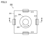
- FIG. 3 is a schematic cross-sectional view showing an example of the configuration of a film forming apparatus.
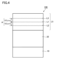
- FIG. 4 is a diagram for explaining a measurement area when measuring the diameter of the maximum inscribed circle of a crystal grain in the first layer.
- FIG. 5 is a diagram for explaining a method for measuring the diameter of the maximum inscribed circle of a crystal grain in the first layer, and is a diagram that typically shows a bright-field image of the measurement field.
- FIG. 6 is a diagram for explaining the positional relationship between the crystal grains and the first and second unit layers.
- the present disclosure therefore aims to provide a cutting tool with a long tool life.
- the cutting tools of the present disclosure can have long tool life.
- a cutting tool according to the present disclosure is a cutting tool including a substrate and a coating provided on the substrate, the coating comprises a first layer and a second layer;
- the second layer is provided at a position closer to the substrate than the first layer,
- the first layer has a multilayer structure in which first unit layers and second unit layers are alternately laminated, the first unit layer has an average thickness of 2 nm or more and 50 nm or less; the second unit layer has an average thickness of 2 nm or more and 50 nm or less;
- the first unit layer is made of Ti a Al 1-a-b B b N, Where: 0.30 ⁇ a ⁇ 0.50, 0 ⁇ b ⁇ 0.10 is satisfied,
- the second unit layer is made of Ti c Al 1-c N, Where: 0.70 ⁇ c ⁇ 1.00 is satisfied, in the first layer, a percentage (T2/T1) ⁇ 100 of the number of titanium atoms T2 to the total number T1 of titanium
- the cutting tools disclosed herein can have a long tool life.
- the nanoindentation hardness of the first layer at 25°C may be 30 GPa or more. This improves the wear resistance of the cutting tool.
- the average thickness of the first layer may be 1.0 ⁇ m or more and 20 ⁇ m or less. This increases the number of first unit layers and second unit layers stacked in the first layer, further improving the effect of suppressing crack growth. This makes it possible to suppress large-scale damage to the coating, and extends the tool life of the cutting tool.
- the average thickness of the second layer may be 0.5 ⁇ m or more and 10 ⁇ m or less. This increases the number of stacked third and fourth unit layers in the second layer, further improving the effect of suppressing crack growth. This makes it possible to suppress large-scale damage to the coating, and extends the tool life of the cutting tool.
- a ⁇ B means the upper and lower limits of a range (i.e., greater than or equal to A and less than or equal to B). If no unit is stated for A and only a unit is stated for B, the units of A and B are the same.
- any one numerical value listed as the lower limit and any one numerical value listed as the upper limit is also considered to be disclosed.
- a1 or more, b1 or more, and c1 or more are listed as the lower limit and a2 or less, b2 or less, and c2 or less are listed as the upper limit, a1 or more and a2 or less, a1 or more and b2 or less, a1 or more and c2 or less, b1 or more and a2 or less, b1 or more and b2 or less, b1 or more and c2 or less, c1 or more and a2 or less, c1 or more and b2 or less, and c1 or more and c2 or less are considered to be disclosed.
- a cutting tool is a cutting tool including a substrate and a coating provided on the substrate, The coating comprises a first layer and a second layer;
- the second layer is provided at a position closer to the substrate than the first layer, the first layer has a multilayer structure in which first unit layers and second unit layers are alternately laminated; the average thickness of the first unit layer is 2 nm or more and 50 nm or less; the average thickness of the second unit layer is 2 nm or more and 50 nm or less;
- the first unit layer is made of Ti a Al 1-a-b B b N, Where: 0.30 ⁇ a ⁇ 0.50, 0 ⁇ b ⁇ 0.10 is satisfied,
- the second unit layer is made of Ti c Al 1-c N, Where: 0.70 ⁇ c ⁇ 1.00 is satisfied, in the first layer, a percentage (T2/T1) ⁇ 100 of the number of titanium atoms T2 to the total number T
- the cutting tool disclosed herein has a long tool life. The reasons for this are believed to be as follows.
- the coating of the cutting tool disclosed herein includes a first layer having a multilayer structure in which first unit layers and second unit layers are alternately stacked.
- the first unit layers and second unit layers have different compositions. This makes it possible to suppress the progression of cracks from the surface of the coating that occur when the cutting tool is used near the interface between the first unit layer and the second unit layer.
- the first unit layer is made of Ti a Al 1-a-b B b N (where 0.30 ⁇ a ⁇ 0.50, 0 ⁇ b ⁇ 0.10 are satisfied).
- the first unit layer has an improved hardness due to the addition of a small amount of boron (B) to TiAlN.
- the second unit layer is made of Ti c Al 1-c N (where 0.70 ⁇ c ⁇ 1.00 is satisfied).
- the second unit layer has a high titanium (Ti) content and excellent high-temperature stability.
- the first layer is made of a multilayer structure in which the high-hardness first unit layer and the high-temperature stability second unit layer are alternately laminated, so that a stable hardness is obtained even at high temperatures and crater wear resistance is improved.
- Crater wear is wear that occurs mainly on the rake face of a cutting tool due to frictional heat between the cutting tool and the cutting chip. Furthermore, since the first layer has a multi-layer structure in which first unit layers having a high hardness and second unit layers having a lower hardness than the first unit layers are alternately laminated, the chipping resistance is also improved, and the crater wear resistance and chipping resistance of the coating are improved in a well-balanced manner, thereby extending the tool life of the cutting tool.
- the first unit layer and the second unit layer have different Ti and Al contents.
- the crystal lattices of the first unit layer and the second unit layer are different, causing distortion of the crystal lattice in the first layer, which allows the first layer to have high hardness. Therefore, the coating including the first layer can have excellent wear resistance.
- the percentage (T2/T1) x 100 of the number of titanium atoms T2 to the total number of titanium and aluminum atoms T1 is 60% or more. This allows the first layer to have excellent crater wear resistance, and extends the tool life of the cutting tool.
- the coating of the cutting tool disclosed herein includes a second layer having a multilayer structure in which third unit layers and fourth unit layers are alternately stacked.
- the third unit layer and the fourth unit layer have different compositions. This makes it possible to suppress the progression of cracks from the surface of the coating that occur when the cutting tool is used near the interface between the third unit layer and the fourth unit layer.
- the second layer has a higher aluminum (Al) content and higher toughness than the first layer. Therefore, a coating having the second layer can have excellent chipping resistance.
- the third unit layer and the fourth unit layer have different Ti contents.
- the third unit layer and the fourth unit layer have different crystal lattices, which causes distortion of the crystal lattice in the second layer, allowing the second layer to have high hardness. Therefore, a coating including the second layer can have excellent abrasion resistance.
- the cutting tool of the first embodiment is not particularly limited in shape, use, etc., as long as it is a cutting tool.
- the cutting tool of the first embodiment may be, for example, a drill, an end mill, a milling cutting insert, a turning cutting insert, a metal saw, a gear cutting tool, a reamer, a tap, or a crankshaft pin milling insert.
- FIG. 1 is a schematic partial cross-sectional view showing an example of the configuration of a cutting tool of embodiment 1.
- the cutting tool 100 includes a substrate 10 and a coating 20 provided on the substrate 10.
- the coating 20 includes a first layer 21 and a second layer 22.
- the second layer 22 is provided at a position closer to the substrate 10 than the first layer 21.
- the first layer 21 has a multilayer structure in which a first unit layer 1 and a second unit layer 2 are alternately stacked.
- the second layer 22 has a multilayer structure in which a third unit layer 3 and a fourth unit layer 4 are alternately stacked.
- the substrate 10 is not particularly limited.
- the substrate 10 may be made of, for example, cemented carbide, cermet, high speed steel, ceramics, cubic boron nitride sintered body, diamond sintered body, etc.
- the substrate 10 is preferably made of cemented carbide. This is because cemented carbide has excellent wear resistance.
- Cemented carbide is a sintered body whose main component is WC (tungsten carbide) particles.
- Cemented carbide includes a hard phase and a binder phase.
- the hard phase contains WC particles.
- the binder phase bonds the WC particles together.
- the binder phase contains, for example, Co (cobalt), etc.
- the binder phase may further contain, for example, TiC (titanium carbide), TaC (tantalum carbide), NbC (niobium carbide), etc.
- Cemented carbide may contain impurities that are inevitably mixed in during the manufacturing process. Cemented carbide may also contain free carbon or an abnormal layer called an " ⁇ layer" in its structure. Furthermore, the cemented carbide may be one that has been subjected to a surface modification treatment. For example, the cemented carbide may contain a de- ⁇ layer on its surface.
- the cemented carbide may contain 85% to 98% by mass of WC particles and 2% to 15% by mass of Co.
- the WC particles may have an average grain size of 0.2 ⁇ m to 4 ⁇ m.
- Co is softer than WC particles.
- the soft Co can be removed by subjecting the surface of the substrate 10 to ion bombardment treatment. Since the cemented carbide has the above composition and the WC particles have the above average particle size, appropriate irregularities are formed on the surface after the Co is removed. It is believed that by forming the coating 20 on such a surface, an anchor effect is exerted, improving the adhesion between the coating 20 and the substrate 10.
- the grain size of the WC grains refers to the diameter of a circle circumscribing a two-dimensional projected image of the WC grains.
- the grain size is measured using a scanning electron microscope (SEM) or a transmission electron microscope (TEM). That is, the cemented carbide is cut and the cut surface is observed with an SEM or TEM.
- the diameter of the circle circumscribing the WC grains is regarded as the grain size of the WC grains.
- the grain sizes of 10 or more (preferably 50 or more, more preferably 100 or more) WC grains randomly selected are measured, and the arithmetic mean value is regarded as the average grain size of the WC grains.
- CP cross section polisher
- FIB focused ion beam
- the coating 20 is provided on the substrate 10.
- the coating 20 may be provided on a part of the surface of the substrate 10, or may be provided on the entire surface. However, the coating 20 is provided on at least a part of the surface of the substrate 10 that corresponds to the cutting edge.
- the part of the surface of the substrate 10 that corresponds to the cutting edge means an area on the surface of the substrate 10 that is within 0.5 mm or 2 mm away from the cutting edge. As long as the effect of the present disclosure is not impaired, even if a coating is not formed on at least a part of the part that corresponds to the cutting edge, it does not deviate from the scope of the present disclosure.
- the coating 20 includes a first layer 21 and a second layer 22.
- the second layer 22 may be provided directly on the substrate 10.
- the first layer 21 may be the outermost layer of the coating 20.
- the coating 20 may be composed of a second layer 22 provided directly on the substrate 10 and a first layer 21 provided directly on the second layer 22.
- the coating 20 may include other layers in addition to the first layer 21 and the second layer 22, as long as the effect of the present disclosure is not impaired.
- the coating 20 may include one or both of a base layer provided between the substrate 10 and the second layer 22 and a surface layer provided on the outermost surface of the coating 20.
- the base layer may include at least one layer selected from the group consisting of a TiCN layer, a TiN layer, and a TiCNO layer.
- the surface layer may include at least one layer selected from the group consisting of a TiC layer, a TiN layer, and a TiCN layer.
- the layered structure of the coating 20 does not need to be uniform across the entire coating 20, and the layered structure may differ in parts.
- the thickness of the coating 20 may be 1.5 ⁇ m or more and 30 ⁇ m or less. When the thickness of the coating 20 is 1.5 ⁇ m or more, abrasion resistance is improved. When the thickness of the coating 20 is 30 ⁇ m or less, chipping resistance is improved.
- the thickness of the coating 20 may be 2.0 ⁇ m or more and 25 ⁇ m or less, or 3.0 ⁇ m or more and 20 ⁇ m or less.
- the thickness of the coating means the sum of the thicknesses of the layers that make up the coating. Examples of "layers that make up the coating" include the first layer, the second layer, the base layer, and the surface layer.
- each layer constituting the coating is measured by obtaining a thin section sample (hereinafter also referred to as "cross-sectional sample") of a cross section parallel to the normal direction of the cutting tool surface, and observing the cross-sectional sample with a scanning transmission electron microscope (STEM).
- STEM scanning transmission electron microscope
- An example of a scanning transmission electron microscope is the JEM-2100F (product name) manufactured by JEOL Ltd.
- the magnification of the cross-sectional sample is set to 5,000 to 10,000 times, and the thickness of each layer is measured at five points, and the arithmetic average value is taken as the "thickness of each layer.”
- the first layer 21 has a multilayer structure in which the first unit layer 1 and the second unit layer 2 are alternately laminated. As long as the average thickness of each of the first unit layer 1 and the second unit layer 2 is 2 nm or more and 50 nm or less, the number of layers is not particularly limited. The number of layers indicates the number of the first unit layer 1 and the second unit layer 2 included in the first layer 21. The number of layers may be 10 or more and 5000 or less, 200 or more and 5000 or less, 400 or more and 2000 or less, or 500 or more and 1000 or less. In the first layer 21, the layer closest to the substrate 10 may be the first unit layer 1 or the second unit layer 2. In the first layer 21, the layer farthest from the substrate 10 may be the first unit layer 1 or the second unit layer 2.
- the average thickness of the first layer can be 1.0 ⁇ m or more and 20 ⁇ m or less. When the average thickness of the first layer is 1.0 ⁇ m or more, the wear resistance is improved. When the average thickness of the first layer is 20 ⁇ m or less, the chipping resistance is improved.
- the lower limit of the average thickness of the first layer may be 1.0 ⁇ m or more, 2.0 ⁇ m or more, or 3.0 ⁇ m or more.
- the upper limit of the average thickness of the first layer may be 20 ⁇ m or less, 18 ⁇ m or less, 16 ⁇ m or less, or 12 ⁇ m or less.
- the average thickness of the first layer may be 1.0 ⁇ m or more and 20 ⁇ m or less, 2.0 ⁇ m or more and 16 ⁇ m or less, or 3.0 ⁇ m or more and 12 ⁇ m or less.
- the average thickness of the first unit layer 1 is 2 nm or more and 50 nm or less
- the average thickness of the second unit layer 2 is 2 nm or more and 50 nm or less.
- the compositions of the first unit layer 1 and the second unit layer 2 may be mixed, and the effect of suppressing crack progress may be reduced.
- the average thickness of one or both of the first unit layer 1 and the second unit layer 2 exceeds 50 nm, the effect of suppressing delamination between layers may be reduced.
- the average thickness of the first unit layer and the average thickness of the second unit layer may be the same or different.
- the lower limit of the average thickness of the first unit layer is 2 nm or more, and may be 4 nm or more, 6 nm or more, or 8 nm or more.
- the upper limit of the average thickness of the first unit layer is 50 nm or less, and may be 46 nm or less, 40 nm or less, or 30 nm or less.
- the average thickness of the first unit layer is 2 nm or more and 50 nm or less, and may be 4 nm or more and 40 nm or less, or 6 nm or more and 30 nm or less.
- the lower limit of the average thickness of the second unit layer is 2 nm or more, and may be 4 nm or more, 6 nm or more, or 8 nm or more.
- the upper limit of the average thickness of the second unit layer is 50 nm or less, and may be 46 nm or less, 40 nm or less, or 30 nm or less.
- the average thickness of the second unit layer is 2 nm or more and 50 nm or less, and may be 4 nm or more and 40 nm or less, or 6 nm or more and 30 nm or less.
- the method for measuring the average thickness of each of the first unit layer and the second unit layer is as follows.
- a thin section sample (hereinafter also referred to as a "cross-sectional sample") of the cutting tool cross section parallel to the normal direction of the cutting tool surface is obtained.
- the cross-sectional sample is observed with a scanning transmission electron microscope (STEM).
- STEM scanning transmission electron microscope
- An example of a scanning transmission electron microscope is JEM-2100F (product name) manufactured by JEOL Ltd.
- the observation magnification of the cross-sectional sample is adjusted appropriately according to the thickness of the first unit layer 1 and the second unit layer 2. For example, the observation magnification can be about 1 million times.
- the thickness is measured at five locations in one first unit layer.
- the arithmetic mean value of the thicknesses of the five locations of the first unit layer is calculated, and the arithmetic mean value is set to the average thickness of the first unit layer.
- the thickness is measured at five locations in one second unit layer.
- the average thickness of the first unit layer is measured using the above procedure.
- the arithmetic mean value of the average thicknesses of the five first unit layers is determined. In the present disclosure, this arithmetic mean value is referred to as the average thickness of the first unit layer.
- the average thickness of the second unit layer is measured using the above procedure.
- the arithmetic mean value of the average thicknesses of the five second unit layers is determined. In the present disclosure, this arithmetic mean value is referred to as the average thickness of the second unit layer.
- the average thicknesses of the third and fourth unit layers described below are also measured in a similar manner as above.
- the first unit layer is made of Ti a Al 1-a-b B b N, where 0.30 ⁇ a ⁇ 0.50 and 0 ⁇ b ⁇ 0.10 are satisfied
- the second unit layer is made of Ti c Al 1-c N, where 0.70 ⁇ c ⁇ 1.00 is satisfied.
- the first unit layer may contain impurities together with Ti a Al 1-a-b B b N, so long as the effects of the present disclosure are not impaired.
- the first unit layer may be made of Ti a Al 1-a-b B b N and impurities.
- the second unit layer may contain impurities together with Ti c Al 1-c N, so long as the effects of the present disclosure are not impaired.
- the second unit layer may be made of Ti c Al 1-c N and impurities. Examples of impurities include carbon (C) and oxygen (O).
- the lower limit of a is 0.30 or more, and may be 0.36 or more, 0.37 or more, or 0.39 or more.
- the upper limit of a is 0.50 or less, and may be 0.48 or less, or 0.45 or less.
- a may be 0.36 ⁇ a ⁇ 0.48, or 0.37 ⁇ a ⁇ 0.45.
- the lower limit of b is greater than 0, and may be 0.01 or greater, 0.02 or greater, or 0.05 or greater.
- the upper limit of b is 0.10 or less, 0.08 or less, or 0.07 or less.
- b may be in the range of 0.01 ⁇ b ⁇ 0.08, or 0.02 ⁇ b ⁇ 0.07.
- the lower limit of c is 0.70 or more, and may be 0.75 or more, 0.80 or more, or 0.87 or more.
- the upper limit of c is 1.00 or less, and may be 0.95 or less, or 0.92 or less. c may be 0.75 ⁇ d ⁇ 0.95, or 0.80 ⁇ d ⁇ 0.92.
- the a and b in Ti a Al 1-a-b B b N of the first unit layer and the c in Ti c Al 1-c N of the second unit layer are identified by measuring the composition of each layer using energy dispersive X-ray spectrometry (EDX).
- EDX energy dispersive X-ray spectrometry
- TEM-DEX transmission electron microscope
- An example of an EDX device is JED-2300 (trademark) manufactured by JEOL Ltd.
- composition analysis is performed as follows: A thin section sample (hereinafter also referred to as a "cross-sectional sample") is obtained from a cross section parallel to the normal direction of the cutting tool surface. While observing the cross-sectional sample with a TEM, EDX analysis is performed at five arbitrarily selected points within one first unit layer or one second unit layer. The first unit layer and the second unit layer can be distinguished by the difference in contrast. Here, the "five arbitrarily selected points" are selected from crystal grains that are different from each other. The composition ratios of each element obtained by measuring the five points are arithmetically averaged to identify the respective compositions of the first unit layer and the second unit layer.
- the composition of the first unit layer is determined by the above procedure.
- the average of the compositions of the five first unit layers is taken as the composition of the first unit layer, and a and b are determined based on this.
- the composition of the second unit layer is determined by the above procedure.
- the average of the compositions of the five second unit layers is taken as the composition of the second unit layer, and c is determined based on this.
- compositions of the third and fourth unit layers described below, as well as d and e in Ti d Al 1-d-e B e N of the third unit layer and f and g in Ti f Al 1-f-g B g N of the fourth unit layer, are also measured in the same manner as above.
- the percentage (T2/T1) ⁇ 100 of the number of titanium atoms T2 relative to the total number T1 of the atoms of titanium and aluminum is 60% or more (hereinafter, also referred to as "percentage (T2/T1) ⁇ 100").
- the lower limit of the percentage (T2/T1) ⁇ 100 is 60% or more, may be 60.0% or more, may be 62.2% or more, may be 62.5% or more, may be 63% or more, may be 63.5% or more, or may be 66% or more.
- the upper limit of the percentage (T2/T1) ⁇ 100 may be 80% or less, may be 77% or less, may be 76.9% or less, or may be 75% or less.
- the percentage (T2/T1) ⁇ 100 may be 60% or more and 80% or less, 63% or more and 77% or less, or 66% or more and 75% or less.
- the percentage (T2/T1) x 100 in the first layer is measured by TEM-EDX.
- An example of an EDX device is the JED-2300 (product name) manufactured by JEOL Ltd.
- the percentage (T2/T1) x 100 is measured by the following procedure.
- a thin section sample (hereinafter also referred to as "cross-sectional sample”) is obtained from a cross section parallel to the normal direction of the cutting tool surface. While observing the cross-sectional sample with a TEM, EDX analysis is performed in five arbitrarily selected fields of view within the first layer, and the percentage (T2/T1) x 100 of the number of titanium atoms T2 relative to the total number of titanium and aluminum atoms T1 is measured. Here, the “five arbitrarily selected fields of view” are set so that they do not overlap with each other. The range of one field of view is 200 x 200 nm. In this disclosure, the arithmetic mean of the percentages (T2/T1) x 100 obtained by measuring the five fields of view is taken as the percentage (T2/T1) x 100 in the first layer.
- the nanoindentation hardness of the first layer at 25°C may be 30 GPa or more. This improves the wear resistance of the cutting tool.
- the lower limit of the nanoindentation hardness may be 32 GPa or more, or 34 GPa or more.
- the upper limit of the nanoindentation hardness H is not particularly limited, but may be 60 GPa or less, 40 GPa or less, or 36 GPa or less from the viewpoint of manufacturing.
- the nanoindentation hardness H may be 30 GPa or more and 60 GPa or less, 32 GPa or more and 60 GPa or less, or 34 GPa or more and 60 GPa or less.
- the nanoindentation hardness of the first layer at 25°C is measured by the nanoindentation method in accordance with the standard procedure defined in "ISO 14577-1: 2015 Metallic materials - Instrumented indentation test for hardness and materials parameters -".
- the measuring instrument used is the "ENT-1100a” manufactured by Elionix.
- the indenter pressing load is 1g. In a cross section parallel to the normal direction of the cutting tool surface, the indenter is pressed against the first layer in the direction perpendicular to the cross section (i.e., parallel to the cutting tool surface).
- the above measurements are performed at five locations on one measurement sample.
- the average nanoindentation hardness of the five locations is the nanoindentation hardness of the first layer. Any data that appears to be abnormal at first glance is to be excluded.
- the first layer may be composed of a plurality of crystal grains, and the diameter of the maximum inscribed circle of the crystal grains may be 5 nm or more and 500 nm or less. This improves the crater wear resistance of the cutting tool.
- the first layer of the present disclosure may include, together with the plurality of crystal grains, a region that does not constitute crystal grains (a region in which the atomic arrangement is random) within a range that does not impair the effects of the present disclosure.
- the upper limit of the diameter of the maximum inscribed circle of the crystal grain may be 500 nm or less, 450 nm or less, or 400 nm or less, from the viewpoint of improving wear resistance and chipping resistance.
- the lower limit of the diameter of the maximum inscribed circle of the crystal grain may be 5 nm or more, 7 nm or more, or 10 nm or more, from the viewpoint of suppressing a decrease in film hardness due to excessive crystal grain refinement.
- the diameter of the maximum inscribed circle of the crystal grain may be 5 nm or more and 500 nm or less, 7 nm or more and 450 nm or less, or 10 nm or more and 400 nm or less.
- the method for measuring the diameter of the maximum inscribed circle of the above crystal grains is as follows.
- a thin section sample (thickness: about 10 to 100 nm, hereinafter also referred to as the "cross-sectional sample") of the cutting tool cross section parallel to the normal direction of the cutting tool surface is obtained.
- the cross-sectional sample is observed with a transmission electron microscope (TEM) to obtain a bright-field image.
- TEM transmission electron microscope
- the bright-field image is obtained so as to include an area A sandwiched between a line L2 that is 0.2 ⁇ m away from a line L1 indicating the center in the average thickness direction of the first layer toward the substrate side, and a line L3 that is 0.2 ⁇ m away from the line L1 toward the surface side of the coating, as shown in Figure 4.
- a rectangular measurement field of view of 150 nm x 150 nm is arbitrarily set within the area A.
- the area where the atomic arrangement is ⁇ 0.5° or less is identified, and this area is defined as a crystal grain.
- the method for identifying the area where the atomic arrangement is ⁇ 0.5° or less and the crystal grain is explained using Figure 5.
- FIG. 5 is a schematic diagram showing an example of a bright-field image of the above-mentioned measurement field.
- atoms are indicated by black dots with the reference number 50. Note that FIG. 5 only shows a portion of the atoms.
- the bright-field image atoms 50 that are regularly arranged are connected by line segments that provide the shortest interatomic distances.
- the line segments are indicated by L10 to L14, L20 to L22, and L30 to L34. Regions where the angle between the line segments is ⁇ 0.5° or less (i.e., -0.5° or more and 0.5° or less) are defined as crystal grains.
- the angle between line segments L10 to L14 is ⁇ 0.5° or less, and the area containing these lines corresponds to crystal grain 24a.
- the angle between line segments L20 to L22 is ⁇ 0.5° or less, and the area containing these lines corresponds to crystal grain 24b.
- the angle between line segments L30 to L34 is ⁇ 0.5° or less, and the area containing these lines corresponds to crystal grain 24c.
- the diameter of the maximum inscribed circle of each crystal grain in the above measurement field is determined.
- the diameter of the maximum inscribed circle means the diameter of the largest inscribed circle that can be drawn inside a crystal grain and that touches at least a part of the outer edge of the crystal grain.
- the diameter of the maximum inscribed circle 25a of crystal grain 24a is D1.
- the diameter of the maximum inscribed circle 25b of crystal grain 24b is D2.
- the diameter of the maximum inscribed circle 25c of crystal grain 24c is D3.
- FIG. 6 is a diagram showing a schematic cross section along the film thickness direction of the first layer of the first embodiment.
- the first layer 21 is made of a multilayer structure in which the first unit layers 1 and the second unit layers 2 are alternately stacked.
- FIG. 6 shows a plurality of crystal grains 24, and the boundaries between the crystal grains 24 are shown as crystal grain boundaries 25.
- Each crystal grain 24 can be made of only the first unit layer or the second unit layer.
- each crystal grain 24 can exist across one or more first unit layers and one or more second unit layers. That is, each crystal grain 24 can have a lamellar structure in which the first unit layers and the second unit layers are alternately stacked.
- the second layer 22 has a multilayer structure in which the third unit layer 3 and the fourth unit layer 4 are alternately laminated. As long as the average thickness of each of the third unit layer 3 and the fourth unit layer 4 is 2 nm or more and 50 nm or less, the number of layers is not particularly limited. The number of layers indicates the number of the third unit layer 3 and the fourth unit layer 4 included in the second layer 22. The number of layers may be 10 or more and 5000 or less, 200 or more and 5000 or less, 400 or more and 2000 or less, or 500 or more and 1000 or less. In the second layer 22, the layer closest to the substrate 10 may be the third unit layer 3 or the fourth unit layer 4. In the second layer 22, the layer farthest from the substrate 10 may be the third unit layer 3 or the fourth unit layer 4.
- the average thickness of the second layer can be 0.5 ⁇ m or more and 10 ⁇ m or less. When the average thickness of the second layer is 0.5 ⁇ m or more, the wear resistance is improved. When the average thickness of the second layer is 10 ⁇ m or less, the chipping resistance is improved.
- the lower limit of the average thickness of the second layer may be 1.0 ⁇ m or more, 2.0 ⁇ m or more, or 3.0 ⁇ m or more.
- the upper limit of the average thickness of the second layer may be 10 ⁇ m or less, 9 ⁇ m or less, 8 ⁇ m or less, or 7 ⁇ m or less.
- the average thickness of the second layer may be 1.0 ⁇ m or more and 9 ⁇ m or less, 2.0 ⁇ m or more and 8 ⁇ m or less, or 3.0 ⁇ m or more and 7 ⁇ m or less.
- ⁇ Average thickness of third unit layer and fourth unit layer> The average thickness of the third unit layer 3 is 2 nm or more and 100 nm or less, and the average thickness of the fourth unit layer 4 is 2 nm or more and 100 nm or less. In the second layer, such thin layers are alternately stacked, thereby suppressing the progress of cracks. If the average thickness of one or both of the third unit layer 3 and the fourth unit layer 4 is less than 2 nm, the compositions of the third unit layer 3 and the fourth unit layer 4 may be mixed, and the effect of suppressing crack progress may be reduced. If the average thickness of one or both of the third unit layer 3 and the fourth unit layer 4 exceeds 100 nm, the effect of suppressing delamination between layers may be reduced. The average thickness of the third unit layer and the average thickness of the fourth unit layer may be the same or different.
- the lower limit of the average thickness of the third unit layer is 2 nm or more, and may be 5 nm or more, 10 nm or more, 15 nm or more, or 20 nm or more.
- the upper limit of the average thickness of the third unit layer is 100 nm or less, and may be 80 nm or less, 75 nm or less, 65 nm or less, or 64 nm or less.
- the average thickness of the third unit layer is 2 nm or more and 100 nm or less, and may be 5 nm or more and 75 nm or less, or 10 nm or more and 65 nm or less.
- the lower limit of the average thickness of the fourth unit layer is 2 nm or more, and may be 5 nm or more, 10 nm or more, 15 nm or more, or 20 nm or more.
- the upper limit of the average thickness of the fourth unit layer is 100 nm or less, and may be 80 nm or less, 75 nm or less, 65 nm or less, 52 nm or less, or 50 nm or less.
- the average thickness of the fourth unit layer is 2 nm or more and 100 nm or less, and may be 5 nm or more and 75 nm or less, or 10 nm or more and 50 nm or less.
- the average thickness of each of the third and fourth unit layers is measured in the same manner as the method for measuring the average thickness of each of the first and second unit layers described above. It has been confirmed that there is no variation in the measurement results even if the measurement points are arbitrarily selected, so long as the measurements are performed using the same cutting tool.
- the third unit layer is made of Ti d Al 1-d-e B e N, where 0.25 ⁇ d ⁇ 0.45 and 0 ⁇ e ⁇ 0.10 are satisfied
- the fourth unit layer is made of Ti f Al 1-f-g B g N, where 0.35 ⁇ f ⁇ 0.55, 0 ⁇ g ⁇ 0.10 and 0.05 ⁇ f-d ⁇ 0.2 are satisfied.
- the third unit layer may contain impurities together with Ti d Al 1-d-e B e N, so long as the effects of the present disclosure are not impaired.
- the third unit layer may be made of Ti d Al 1-d-e B e N and impurities.
- the fourth unit layer may contain impurities together with Ti f Al 1-f-g B g N, so long as the effects of the present disclosure are not impaired.
- the fourth unit layer may be composed of Ti f Al 1-f-g B g N and impurities, such as carbon (C) and oxygen (O).
- the lower limit of d is 0.25 or more, and may be 0.30 or more, 0.31 or more, 0.32 or more, 0.33 or more, or 0.34 or more.
- the upper limit of d is less than 0.45, and may be 0.40 or less, 0.37 or less, or 0.35 or less.
- d may be 0.30 ⁇ d ⁇ 0.40, or 0.31 ⁇ d ⁇ 0.37.
- the lower limit of e is greater than 0, and may be 0.01 or greater, 0.02 or greater, 0.04 or greater, or 0.05 or greater.
- the upper limit of e is 0.10 or less, 0.08 or less, 0.07 or less, or 0.06 or less. e may be in the range of 0.01 ⁇ e ⁇ 0.08, or 0.02 ⁇ e ⁇ 0.07.
- the lower limit of f is 0.35 or more, and may be 0.40 or more, 0.41 or more, 0.42 or more, 0.43 or more, or 0.45 or more.
- the upper limit of f is less than 0.55 and may be 0.50 or less.
- c may be 0.40 ⁇ f ⁇ 0.55, or 0.45 ⁇ f ⁇ 0.50.
- the lower limit of g is greater than 0, and may be 0.01 or greater, 0.02 or greater, or 0.04 or greater.
- the upper limit of g is 0.10 or less, 0.08 or less, or 0.06 or less.
- c may be 0.01 ⁇ f ⁇ 0.10, or 0.02 ⁇ f ⁇ 0.06.
- the lower limit of f-d is 0.05 or more, and may be 0.08 or more, 0.10 or more, or 0.11 or more.
- the upper limit of f-d is 0.20 or less, and may be 0.18 or less.
- f-d may be 0.08 ⁇ f-d ⁇ 0.18, or 0.10 ⁇ f-d ⁇ 0.18.
- the ratio I(200)/I(002) of the peak intensity I(200) derived from the (200) plane to the peak intensity I(002) derived from the (002) plane is 2 or more, and the half-width of the peak derived from the (002) plane is 2 degrees or more. This improves the hardness and toughness of the second layer, and excellent wear resistance and chipping resistance can be obtained.
- the "peak intensity I(002) derived from the (002) plane” means the diffraction intensity (peak height) of the highest peak among the X-ray diffraction peaks derived from the (002) plane of the hexagonal crystal.
- the "peak intensity I(200) derived from the (200) plane” means the diffraction intensity (peak height) of the highest peak among the X-ray diffraction peaks derived from the (200) plane of the cubic crystal. If a peak derived from the (002) plane of the hexagonal crystal is present in the X-ray diffraction spectrum of the second layer, it is confirmed that the second layer contains a hexagonal crystal structure. When the X-ray diffraction spectrum of the second layer shows a peak derived from the (200) plane of a cubic crystal, it is confirmed that the second layer contains a cubic crystal structure.
- the ratio I(200)/I(002) of 2 or more means that a mixed crystal of a cubic crystal and a hexagonal crystal is formed in the second layer.
- the conditions of the X-ray diffraction analysis for measuring the peak intensity I(002) and the peak intensity I(200) are as follows.
- Detector 0-dimensional detector (scintillation counter)
- Receiving optical system Use of analyzer crystal (PW3098/27) Step: 0.03° Integration time: 2 seconds
- X-ray diffraction measurement is performed by the ⁇ /2 ⁇ method at each of three arbitrary locations in the second layer to determine the X-ray diffraction intensity of a specified crystal plane, and the average of the X-ray diffraction intensities at the three locations is regarded as the X-ray diffraction intensity of the specified crystal plane.
- Examples of devices used for X-ray diffraction measurement include "SmartLab" (product name) manufactured by Rigaku Corporation and "X'pert" (product name) manufactured by PANalytical Corporation.
- the lower limit of the ratio I(200)/I(002) is 2 or more, and may be 2.0 or more, 2.2 or more, or 2.3 or more.
- the upper limit of the ratio I(200)/I(002) may be, for example, 10 or less, less than 10, 5 or less, or 3 or less.
- the ratio I(200)/I(002) may be 2 or more and 10 or less, or 2 or more and 5 or less.
- the fact that the half-width of the peak derived from the (002) plane is 2 degrees or more means that hexagonal crystals are finely dispersed in the second layer, improving hardness and toughness.
- the lower limit of the half-width of the peak derived from the (002) plane is 2 degrees or more, and may be 2.0 degrees or more, or 2.2 degrees or more.
- the upper limit of the half-width of the peak derived from the (002) plane may be 4 degrees or less, or may be 3 degrees or less.
- the lower limit of the half-width of the peak derived from the (002) plane may be 2 degrees or more, and may be 2.2 degrees or more, or 2.4 degrees or more.
- the half-width of the peak derived from the (002) plane may be 2 degrees or more and 4 degrees or less, or may be 2 degrees or more and 3 degrees or less.
- Embodiment 2 Manufacturing method of cutting tool
- a method for manufacturing the cutting tool of embodiment 1 will be described.
- the manufacturing method of embodiment 2 can include a step of preparing a substrate and a step of forming a coating on the substrate. Each step will be described in detail below.
- a substrate 10 is prepared.
- the substrate 10 may be the substrate described in the first embodiment.
- the coating 20 is formed on the substrate 10.
- the coating 20 can be formed by a physical vapor deposition (PVD) method.
- PVD physical vapor deposition
- Specific examples of the PVD method include an arc ion plating (AIP) method, a balanced magnetron sputtering (BMS) method, and an unbalanced magnetron sputtering (UBMS) method.
- AIP arc ion plating
- BMS balanced magnetron sputtering
- UBMS unbalanced magnetron sputtering
- an arc discharge is generated using the target material as a negative electrode (cathode). This causes the target material to evaporate and ionize. The ions are then deposited on the surface of the substrate 10 to which a negative bias voltage is applied.
- the AIP method is superior in terms of the ionization rate of the target material.
- the film forming apparatus 200 includes a chamber 201.
- the chamber 201 is provided with a gas inlet 202 for introducing a source gas into the chamber 201, and a gas exhaust port 203 for discharging the source gas from the chamber 201 to the outside.
- the gas exhaust port 203 is connected to a vacuum pump (not shown). The pressure inside the chamber 201 is adjusted by the amount of gas introduced and discharged.
- a rotating table 204 is disposed within the chamber 201.
- a substrate holder 205 for holding the substrate 10 is attached to the rotating table 204.
- the substrate holder 205 is connected to the negative terminal of a bias power supply 206.
- the positive terminal of the bias power supply 206 is earthed.
- a number of target materials 211, 212, 213, and 214 are attached to the side wall of the chamber 201.
- each of the target materials 211 and 212 is connected to the negative terminal of a DC power supply 221 or 222, respectively.
- the DC power supplies 221 and 222 are variable power supplies, and their positive terminals are earthed.
- the target materials 213 and 214 The specific operation will be described below.
- the substrate 10 is held by the substrate holder 205.
- the pressure inside the chamber 201 is adjusted to 1.0 ⁇ 10 ⁇ 4 Pa using a vacuum pump. While the turntable 204 is rotating, the temperature of the substrate 10 is adjusted to 500° C. by a heater (not shown) attached to the film forming apparatus 200.
- Ar gas is introduced from the gas inlet 202, and the pressure inside the chamber 201 is adjusted to 3.0 Pa. While maintaining the same pressure, the voltage of the bias power supply 206 is gradually changed and finally adjusted to -1000 V. The surface of the substrate 10 is then cleaned by ion bombardment processing using Ar ions.
- the underlayer is formed on the surface of the substrate 10.
- a TiCN layer, a TiN layer, or a TiCNO layer is formed on the surface of the substrate 10.
- a second layer is formed on the surface of the substrate 10 or on the surface of the underlayer.
- the composition of each target material is selected so as to obtain the composition of the third and fourth unit layers.
- Each target material is set in a predetermined position, nitrogen gas is introduced from the gas inlet 202, and the second layer is formed while rotating the turntable 204.
- the substrate is maintained at a temperature of 400-800°C, the reactive gas pressure is maintained at 1-10 Pa (nitrogen gas partial pressure is 5-10 Pa), and an arc current of 80-200 A is alternately supplied to the evaporation source for forming the third unit layer and the evaporation source for forming the fourth unit layer while gradually changing the voltage of the bias power supply in the range of 30-200 V (DC power supply).
- metal ions are generated from the evaporation source for forming the third unit layer and the evaporation source for forming the fourth unit layer, and when the substrate faces the evaporation source for forming the third unit layer, the third unit layer is formed, and when the substrate faces the evaporation source for forming the fourth unit layer, the fourth unit layer is formed.
- the film while changing the voltage of the bias power supply as described above, it is possible to achieve both high hardness and cutting edge quality of the second layer.
- the supply of the arc current is stopped when a predetermined time has elapsed.
- the rotation speed of the substrate is adjusted to adjust the thickness of each of the third unit layer and the fourth unit layer.
- the thickness of the second layer is adjusted to be within a predetermined range by adjusting the film formation time.
- the second layer may be formed on the surface of the substrate other than the part involved in the cutting process.
- the substrate may be maintained at a temperature of 500-600°C, the reactive gas pressure at 5-10 Pa (nitrogen gas partial pressure 5-8 Pa), and the voltage of the bias power supply may be gradually changed in the range of 30-200 V (DC power supply) while an arc current of 80-120 A is alternately supplied to the evaporation source for forming the third unit layer and the evaporation source for forming the fourth unit layer.
- the reactive gas pressure at 5-10 Pa (nitrogen gas partial pressure 5-8 Pa
- the voltage of the bias power supply may be gradually changed in the range of 30-200 V (DC power supply) while an arc current of 80-120 A is alternately supplied to the evaporation source for forming the third unit layer and the evaporation source for forming the fourth unit layer.
- the composition of each target material is selected so as to obtain the composition of the first unit layer and the second unit layer.
- Each target material is set in a predetermined position, and nitrogen gas is introduced from the gas inlet 202.
- the first layer is formed while rotating the turntable 204.
- the conditions for forming the first layer are as follows.
- the substrate temperature, reaction gas pressure, bias voltage and arc current are either constant within the above ranges or are continuously changed within the above ranges.
- the multilayer structure in which the first unit layers and the second unit layers are alternately laminated can be formed by appropriately combining the following methods (A) to (D).
- A) In the AIP method a plurality of target materials (sintered alloys) having different compositions are used.
- D In the AIP method, the substrate 10 is rotated and the rotation period is controlled.
- the coating includes a surface layer
- the surface layer is formed, for example, on the surface of the first layer.
- a cutting tool 100 can be manufactured that includes a substrate 10 and a coating 20 provided on the substrate 10.
- a cutting tip made of cemented carbide (model number: CNMG120408 (manufactured by Sumitomo Electric Hardmetal)) was prepared as the substrate.
- the cemented carbide contains WC particles (90% by mass) and Co (10% by mass).
- the average particle size of the WC particles is 1 to 2 ⁇ m.
- a coating was formed on the substrate using a film-forming apparatus having the configuration shown in Figures 2 and 3.
- the specific conditions for the ion bombardment treatment are as described in embodiment 2.
- the target material was then set in a predetermined position in the film forming device.
- the composition of each target material was adjusted to obtain the compositions of the first and second unit layers shown in Table 1, and the compositions of the third and fourth unit layers shown in Table 2.
- the second layer was formed on the substrate. Specifically, nitrogen gas was introduced from the gas inlet, and the third and fourth unit layers were alternately formed while the turntable was rotating, thereby forming the second layer.
- the substrate was maintained at a temperature of 550°C, the reactive gas pressure at 8 Pa (nitrogen gas partial pressure: 8 Pa), and an arc current of 90 A was alternately supplied to the evaporation source for forming the third unit layer and the evaporation source for forming the fourth unit layer while the voltage of the bias power supply was gradually changed in the range of 35 to 180 V.
- the thickness and number of layers of the third and fourth unit layers were adjusted by the rotation speed of the substrate.
- the first layer was formed on the second layer. Specifically, nitrogen gas was introduced from the gas inlet, and the first and second unit layers were alternately formed while rotating the turntable, thereby forming the first layer on the second layer.
- the conditions for forming the first layer of each sample were a substrate temperature of 400 to 800°C, a bias voltage of -400 to -20V, an arc current of 80 to 200A, and a reaction gas pressure of 2 to 10Pa.
- the substrate temperature, reaction gas pressure, bias voltage, and arc current were either constant within the above ranges, or were changed continuously within the above ranges.
- the thickness and number of layers of each of the first and second unit layers were adjusted by the rotation speed of the substrate. Through the above process, cutting tools for each sample were obtained.
- ⁇ Evaluation> ⁇ Coating composition> For the coating of each sample, the composition, average thickness, number of stacks, average thickness of the first layer and the second layer, percentage of the number of titanium atoms to the total number of titanium and aluminum atoms in the first layer (shown as "(T2/T1) x 100" in Table 1), nanoindentation hardness of the first layer (shown as “hardness” in Table 1), ratio I(200)/I(002) of the second layer, and half width of the peak derived from the (002) plane (shown as "(002) peak half width” in Table 2) were measured.
- the measurement method for each item is as described in embodiment 1.
- the results are shown in Tables 1 and 2.
- Table 1 the notation "1" for "number of stacks” indicates that only one first unit layer or one second unit layer was formed.
- the notation "-" indicates that the corresponding layer was not formed.
- Samples 1 to 15 correspond to the examples.
- Samples 21 to 28 correspond to the comparative examples. It was confirmed that Samples 1 to 15 had a longer tool life than Samples 21 to 28.
Landscapes
- Chemical & Material Sciences (AREA)
- Engineering & Computer Science (AREA)
- Mechanical Engineering (AREA)
- Chemical Kinetics & Catalysis (AREA)
- Materials Engineering (AREA)
- Metallurgy (AREA)
- Organic Chemistry (AREA)
- Inorganic Chemistry (AREA)
- Ceramic Engineering (AREA)
- Cutting Tools, Boring Holders, And Turrets (AREA)
- Physical Vapour Deposition (AREA)
- Drilling Tools (AREA)
Abstract
Description
前記被膜は、第1層および第2層を含み、
前記第2層は、前記第1層よりも前記基材に近い位置に設けられ、
前記第1層は、第1単位層と第2単位層とが交互に積層された多層構造からなり、
前記第1単位層の平均厚さは、2nm以上50nm以下であり、
前記第2単位層の平均厚さは、2nm以上50nm以下であり、
前記第1単位層は、TiaAl1-a-bBbNからなり、
ここで、
0.30≦a≦0.50、
0<b≦0.10、を満たし、
前記第2単位層は、TicAl1-cNからなり、
ここで、
0.70≦c≦1.00、を満たし、
前記第1層において、チタンおよびアルミニウムの原子数の合計T1に対する、チタンの原子数T2の百分率(T2/T1)×100は、60%以上であり、
前記第2層は、第3単位層と第4単位層とが交互に積層された多層構造からなり、
前記第3単位層の平均厚さは、2nm以上100nm以下であり、
前記第4単位層の平均厚さは、2nm以上100nm以下であり、
前記第3単位層は、TidAl1-d-eBeNからなり、
前記第4単位層は、TifAl1-f-gBgNからなり、
ここで、
0.25≦d<0.45、
0<e≦0.10、
0.35≦f<0.55、
0<g≦0.10、
0.05≦f-d≦0.20、を満たし、
前記第2層のX線回折スペクトルにおいて、(002)面に由来するピーク強度I(002)に対する、(200)面に由来するピーク強度I(200)の割合I(200)/I(002)は、2以上であり、かつ、前記(002)面に由来するピークの半値幅は2度以上である、切削工具である。
近年、コスト低減の要求が益々高まっており、工具の長寿命化が求められている。例えば、ステンレス鋼の旋削加工においても、長い工具寿命を有する切削工具が求められている。
本開示の切削工具は、長い工具寿命を有することができる。
最初に本開示の実施態様を列記して説明する。
(1)本開示の切削工具は、基材と、前記基材上に設けられた被膜と、を備える切削工具であって、
前記被膜は、第1層および第2層を含み、
前記第2層は、前記第1層よりも前記基材に近い位置に設けられ、
前記第1層は、第1単位層と第2単位層とが交互に積層された多層構造からなり、
前記第1単位層の平均厚さは、2nm以上50nm以下であり、
前記第2単位層の平均厚さは、2nm以上50nm以下であり、
前記第1単位層は、TiaAl1-a-bBbNからなり、
ここで、
0.30≦a≦0.50、
0<b≦0.10、を満たし、
前記第2単位層は、TicAl1-cNからなり、
ここで、
0.70≦c≦1.00、を満たし、
前記第1層において、チタンおよびアルミニウムの原子数の合計T1に対する、チタンの原子数T2の百分率(T2/T1)×100は、60%以上であり、
前記第2層は、第3単位層と第4単位層とが交互に積層された多層構造からなり、
前記第3単位層の平均厚さは、2nm以上100nm以下であり、
前記第4単位層の平均厚さは、2nm以上100nm以下であり、
前記第3単位層は、TidAl1-d-eBeNからなり、
前記第4単位層は、TifAl1-f-gBgNからなり、
ここで、
0.25≦d<0.45、
0<e≦0.10、
0.35≦f<0.55、
0<g≦0.10、
0.05≦f-d≦0.20、を満たし、
前記第2層のX線回折スペクトルにおいて、(002)面に由来するピーク強度I(002)に対する、(200)面に由来するピーク強度I(200)の割合I(200)/I(002)は、2以上であり、かつ、前記(002)面に由来するピークの半値幅は2度以上である、切削工具である。
本開示の切削工具の具体例を、以下に図面を参照しつつ説明する。本開示の図面において、同一の参照符号は、同一部分または相当部分を表すものである。また、長さ、幅、厚さ、深さなどの寸法関係は図面の明瞭化と簡略化のために適宜変更されており、必ずしも実際の寸法関係を表すものではない。
本開示の一実施形態(以下、「実施形態1」とも記す。)の切削工具は、基材と、該基材上に設けられた被膜と、を備える切削工具であって、
該被膜は、第1層および第2層を含み、
該第2層は、該第1層よりも該基材に近い位置に設けられ、
該第1層は、第1単位層と第2単位層とが交互に積層された多層構造からなり、
該第1単位層の平均厚さは、2nm以上50nm以下であり、
該第2単位層の平均厚さは、2nm以上50nm以下であり、
該第1単位層は、TiaAl1-a-bBbNからなり、
ここで、
0.30≦a≦0.50、
0<b≦0.10、を満たし、
該第2単位層は、TicAl1-cNからなり、
ここで、
0.70≦c≦1.00、を満たし、
該第1層において、チタンおよびアルミニウムの原子数の合計T1に対する、チタンの原子数T2の百分率(T2/T1)×100は、60%以上であり、
該第2層は、第3単位層と第4単位層とが交互に積層された多層構造からなり、
該第3単位層の平均厚さは、2nm以上100nm以下であり、
該第4単位層の平均厚さは、2nm以上100nm以下であり、
該第3単位層は、TidAl1-d-eBeNからなり、
該第4単位層は、TifAl1-f-gBgNからなり、
ここで、
0.25≦d<0.45、
0<e≦0.10、
0.35≦f<0.55、
0<g≦0.10、
0.05≦f-d≦0.20、を満たし、
該第2層のX線回折スペクトルにおいて、(002)面に由来するピーク強度I(002)に対する、(200)面に由来するピーク強度I(200)の割合I(200)/I(002)は、2以上であり、かつ、該(002)面に由来するピークの半値幅は2度以上である、切削工具である。
実施形態1の切削工具は、切削工具である限り、その形状および用途等は、特に限定されない。実施形態1の切削工具は、たとえば、ドリル、エンドミル、フライス加工用刃先交換型チップ、旋削加工用刃先交換型チップ、メタルソー、歯切工具、リーマ、タップまたはクランクシャフトのピンミーリング加工用チップ等であり得る。
基材10は、特に限定されない。基材10は、例えば、超硬合金、サーメット、高速度鋼、セラミックス、立方晶窒化硼素焼結体、およびダイヤモンド焼結体等により構成され得る。基材10は、好ましくは超硬合金製である。超硬合金は、耐摩耗性に優れるためである。
被膜20は、基材10上に設けられている。被膜20は、基材10の表面の一部に設けられていてもよいし、全面に設けられていてもよい。ただし、被膜20は、基材10の表面のうち、少なくとも切れ刃に相当する部分に設けられているものとする。本開示において、基材10の表面の切れ刃に相当する部分とは、基材10の表面において、刃先稜線からの距離が0.5mm以内、または、2mm以内の領域を意味する。本開示の効果を損なわない限り、切れ刃に相当する部分の少なくとも一部に被膜が形成されていなくても、本開示の範囲を逸脱するものではない。
第1層21は、第1単位層1と第2単位層2とが交互に積層された多層構造からなる。第1単位層1および第2単位層2のそれぞれの平均厚さが2nm以上50nm以下である限り、積層数は、特に限定されない。積層数とは、第1層21に含まれる第1単位層1および第2単位層2のそれぞれの数を示す。積層数は、10以上5000以下でもよく、200以上5000以下でもよく、400以上2000以下でもよく、500以上1000以下でもよい。第1層21において、最も基材10に近い層は、第1単位層1であってもよいし、第2単位層2であってもよい。また第1層21において、最も基材10から離れている層は、第1単位層1であってもよいし、第2単位層2であってもよい。
第1単位層1の平均厚さは、2nm以上50nm以下であり、第2単位層2の平均厚さは、2nm以上50nm以下である。第1層において、このような薄層が交互に積層されることにより、亀裂の進展を抑制できる。第1単位層1および第2単位層2の一方または両方の平均厚さが2nm未満になると、第1単位層1および第2単位層2の組成が混ざり合って、亀裂進展の抑制効果が低減する可能性がある。第1単位層1および第2単位層2の一方または両方の平均厚さが50nm超であると、層間剥離の抑制効果が低減する可能性がある。第1単位層の平均厚さと、第2単位層の平均厚さとは、同一であってもよいし、異なっていてもよい。
本開示の切削工具において、第1単位層は、TiaAl1-a-bBbNからなり、ここで、0.30≦a≦0.50、0<b≦0.10、を満たし、第2単位層は、TicAl1-cNからなり、ここで、0.70≦c≦1.00、を満たす。本開示の効果を損なわない限り、第1単位層はTiaAl1-a-bBbNとともに不純物を含むことができる。第1単位層は、TiaAl1-a-bBbNと不純物とからなることができる。本開示の効果を損なわない限り、第2単位層はTicAl1-cNとともに不純物を含むことができる。第2単位層は、TicAl1-cNと不純物とからなることができる。不純物としては、例えば、炭素(C)、酸素(O)が挙げられる。
第1層において、チタンおよびアルミニウムの原子数の合計T1に対する、チタンの原子数T2の百分率(T2/T1)×100(以下、「百分率(T2/T1)×100」とも記す。)は、60%以上である。これによると、第1層は優れた耐クレータ摩耗性を有することができる。百分率(T2/T1)×100の下限は、耐クレータ摩耗性向上の観点から、60%以上であり、60.0%以上でもよく、62.2%以上でもよく、62.5%以上でもよく、63%以上でもよく、63.5%以上でもよく、66%以上でもよい。百分率(T2/T1)×100の上限は、耐酸化性向上の観点から、80%以下でもよく、77%以下でもよく、76.9%以下でもよく、75%以下でもよい。百分率(T2/T1)×100は、60%以上80%以下でもよく、63%以上77%以下でもよく、66%以上75%以下でもよい。
25℃における第1層のナノインデンテーション硬さは、30GPa以上でもよい。これによると、切削工具の耐摩耗性が向上する。ナノインデンテーション硬さの下限は、32GPa以上でもよく、34GPa以上でもよい。ナノインデンテーション硬さHの上限は、特に制限されないが、製造上の観点から、60GPa以下でもよく、40GPa以下でもよく、36GPa以下でもよい。ナノインデンテーション硬さHは30GPa以上60GPa以下でもよく、32GPa以上60GPa以下でもよく、34GPa以上60GPa以下でもよい。
第1層は複数の結晶粒からなり、該結晶粒の最大内接円の直径は5nm以上500nm以下であってもよい。これによると、切削工具の耐クレータ摩耗性が向上する。本開示の第1層は、本開示の効果を損なわない範囲において、複数の結晶粒とともに、結晶粒を構成しない領域(原子配列がランダムな領域)を含んでいてもよい。
結晶粒と第1単位層および第2単位層との位置関係について、図6を用いて説明する。図6は、実施形態1の第1層の膜厚方向に沿う断面を模式的に示す図である。図6に示される通り、第1層21は、第1単位層1と第2単位層2とが交互に積層された多層構造からなる。図6には、複数の結晶粒24が示されており、結晶粒24間の境界は、結晶粒界25として示される。各結晶粒24は、第1単位層または第2単位層のみからなることができる。また、各結晶粒24は、1層以上の第1単位層および1層以上の第2単位層にまたがって存在することができる。すなわち、各結晶粒24は、第1単位層と第2単位層とが交互に積層されたラメラ構造を有することができる。
第2層22は、第3単位層3と第4単位層4とが交互に積層された多層構造からなる。第3単位層3および第4単位層4のそれぞれの平均厚さが2nm以上50nm以下である限り、積層数は、特に限定されない。積層数とは、第2層22に含まれる第3単位層3および第4単位層4のそれぞれの数を示す。積層数は、10以上5000以下でもよく、200以上5000以下でもよく、400以上2000以下でもよく、500以上1000以下でもよい。第2層22において、最も基材10に近い層は、第3単位層3であってもよいし、第4単位層4であってもよい。また第2層22において、最も基材10から離れている層は、第3単位層3であってもよいし、第4単位層4であってもよい。
第3単位層3の平均厚さは、2nm以上100nm以下であり、第4単位層4の平均厚さは、2nm以上100nm以下である。第2層において、このような薄層が交互に積層されることにより、亀裂の進展を抑制できる。第3単位層3および第4単位層4の一方または両方の平均厚さが2nm未満になると、第3単位層3および第4単位層4の組成が混ざり合って、亀裂進展の抑制効果が低減する可能性がある。第3単位層3および第4単位層4の一方または両方の平均厚さが100nm超であると、層間剥離の抑制効果が低減する可能性がある。第3単位層の平均厚さと、第4単位層の平均厚さとは、同一であってもよいし、異なっていてもよい。
本開示の切削工具において、第3単位層は、TidAl1-d-eBeNからなり、ここで、0.25≦d<0.45、0<e≦0.10を満たし、第4単位層は、TifAl1-f-gBgNからなり、ここで、0.35≦f<0.55、0<g≦0.10、0.05≦f-d≦0.2を満たす。本開示の効果を損なわない限り、第3単位層はTidAl1-d-eBeNとともに不純物を含むことができる。第3単位層は、TidAl1-d-eBeNと不純物とからなることができる。本開示の効果を損なわない限り、第4単位層はTifAl1-f-gBgNとともに不純物を含むことができる。第4単位層は、TifAl1-f-gBgNと不純物とからなることができる。該不純物としては、例えば、炭素(C)、酸素(O)が挙げられる。
第2層のX線回折スペクトルにおいて、(002)面に由来するピーク強度I(002)に対する、(200)面に由来するピーク強度I(200)の割合I(200)/I(002)は、2以上であり、かつ、(002)面に由来するピークの半値幅は2度以上である。これによると、第2層の硬度および靭性が向上し、優れた耐摩耗性および耐欠損性を得ることができる。「(002)面に由来するピーク強度I(002)」とは、六方晶の(002)面に由来するX線回折ピークのうち、最も高いピークにおける回折強度(ピークの高さ)を意味する。「(200)面に由来するピーク強度I(200)」とは、立方晶の(200)面に由来するX線回折ピークのうち、最も高いピークにおける回折強度(ピークの高さ)を意味する。第2層のX線回折スペクトルにおいて、六方晶の(002)面に由来するピークが存在する場合、第2層は六方晶型の結晶構造を含むことが確認される。第2層のX線回折スペクトルにおいて、立方晶の(200)面に由来するピークが存在する場合、第2層は立方晶型の結晶構造を含むことが確認される。比I(200)/I(002)が2以上であることは、第2層において立方晶と六方晶との混晶が形成されていることを意味する。
走査軸:2θ-θ
X線源:Cu-Kα線(1.541862Å)
検出器:0次元検出器(シンチレーションカウンタ)
管電圧:45kV
管電流:40mA
入射光学系:ミラーの利用
受光光学系:アナライザ結晶(PW3098/27)の利用
ステップ:0.03°
積算時間:2秒
スキャン範囲(2θ):20°~80°
実施形態2では、実施形態1の切削工具の製造方法について説明する。実施形態2の製造方法は、基材を準備する工程と、該基材上に被膜を形成する工程とを含むことができる。各工程の詳細について、以下に説明する。
基材を準備する工程では、基材10が準備される。基材10は、実施形態1に記載の基材を用いることができる。
被膜を形成する工程では、基材10上に被膜20を形成する。実施形態2では、物理蒸着(Physical Vapor Deposition;PVD)法により、被膜20を形成することができる。PVD法の具体例としては、アークイオンプレーティング(Arc Ion Plating;AIP)法、バランスドマグネトロンスパッタリング(Balanced Magnetron Sputtering;BMS)法、およびアンバランスドマグネトロンスパッタリング(Unbalanced Magnetron Sputtering;UBMS)法等が挙げられる。実施形態2では、アークイオンプレーティングを用いることが好ましい。
基材温度 :400~800℃
バイアス電圧:-400~-20V
アーク電流 :80~200A
反応ガス圧 :2~10Pa
(A)AIP法において、組成が互いに異なる複数のターゲット材(焼結合金)を用いる。
(B)AIP法において、成膜中、基材10に印加されるバイアス電圧を上記の第1層の形成条件に記載のバイアス電圧内で変化させる。
(C)AIP法において、ガス流量を変化させる。
(D)AIP法において、基材10を回転させ、その回転周期を制御する。
<切削工具の作製>
以下のようにして、切削工具を作製し、工具寿命を評価した。
≪被膜の構成≫
各試料の被膜について、第1単位層、第2単位層、第3単位層および第4単位層の組成、平均厚さ、積層数、第1層および第2層の平均厚さ、第1層におけるチタンおよびアルミニウムの原子数の合計に対するチタンの原子数の百分率(表1において「(T2/T1)×100」と示す。)、第1層のナノインデンテーション硬さ(表1において「硬さ」と示す。)、第2層の割合I(200)/I(002)、(002)面に由来するピークの半値幅(表2において「(002)ピーク半値幅」と示す。)を測定した。各項目の測定方法は実施形態1に記載の通りである。結果を表1および表2に示す。表1において、「積層数」が「1」との表記は、第1単位層または第2単位層を1層のみ形成したことを示す。表1において「-」との表記は、該当する層を形成しなかったことを示す。


各試料の切削工具を用いて以下の条件で旋削加工を行い、逃げ面から測定した欠損の幅が0.5mm以上となるまでの切削距離を測定した。切削距離が長いほど、耐クレータ摩耗性および耐欠損性に優れ、工具寿命が長いことを示す。結果を表3の「切削試験」の「切削距離」欄に示す。
被削材:SUS316 丸材
切削速度:200m/min
送り量:0.2mm/rev
切り込み量:1.5mm
湿式
上記の切削条件は、ステンレス鋼の旋削加工(高速加工)に該当する。
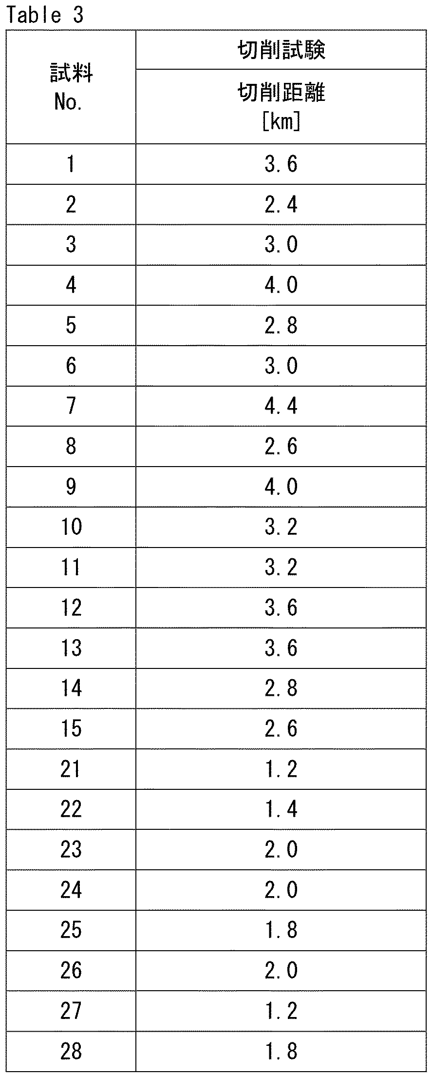
試料1~試料15は実施例に該当する。試料21~試料28は比較例に該当する。試料1~試料15は試料21~試料28よりも、工具寿命が長いことが確認された。
今回開示された実施の形態および実施例はすべての点で例示であって、制限的なものではないと考えられるべきである。本開示の範囲は上記した実施の形態および実施例ではなく請求の範囲によって示され、請求の範囲と均等の意味、および範囲内でのすべての変更が含まれることが意図される。
Claims (4)
- 基材と、前記基材上に設けられた被膜と、を備える切削工具であって、
前記被膜は、第1層および第2層を含み、
前記第2層は、前記第1層よりも前記基材に近い位置に設けられ、
前記第1層は、第1単位層と第2単位層とが交互に積層された多層構造からなり、
前記第1単位層の平均厚さは、2nm以上50nm以下であり、
前記第2単位層の平均厚さは、2nm以上50nm以下であり、
前記第1単位層は、TiaAl1-a-bBbNからなり、
ここで、
0.30≦a≦0.50、
0<b≦0.10、を満たし、
前記第2単位層は、TicAl1-cNからなり、
ここで、
0.70≦c≦1.00、を満たし、
前記第1層において、チタンおよびアルミニウムの原子数の合計T1に対する、チタンの原子数T2の百分率(T2/T1)×100は、60%以上であり、
前記第2層は、第3単位層と第4単位層とが交互に積層された多層構造からなり、
前記第3単位層の平均厚さは、2nm以上100nm以下であり、
前記第4単位層の平均厚さは、2nm以上100nm以下であり、
前記第3単位層は、TidAl1-d-eBeNからなり、
前記第4単位層は、TifAl1-f-gBgNからなり、
ここで、
0.25≦d<0.45、
0<e≦0.10、
0.35≦f<0.55、
0<g≦0.10、
0.05≦f-d≦0.20、を満たし、
前記第2層のX線回折スペクトルにおいて、(002)面に由来するピーク強度I(002)に対する、(200)面に由来するピーク強度I(200)の割合I(200)/I(002)は、2以上であり、かつ、前記(002)面に由来するピークの半値幅は2度以上である、切削工具。 - 25℃における前記第1層のナノインデンテーション硬さは、30GPa以上である、請求項1に記載の切削工具。
- 前記第1層の平均厚さは、1.0μm以上20μm以下である、請求項1または請求項2に記載の切削工具。
- 前記第2層の平均厚さは、0.5μm以上10μm以下である、請求項1から請求項3のいずれか1項に記載の切削工具。
Priority Applications (6)
| Application Number | Priority Date | Filing Date | Title |
|---|---|---|---|
| PCT/JP2023/016837 WO2024224595A1 (ja) | 2023-04-28 | 2023-04-28 | 切削工具 |
| JP2023540771A JP7552986B1 (ja) | 2023-04-28 | 2023-04-28 | 切削工具 |
| CN202380042501.3A CN119255879A (zh) | 2023-04-28 | 2023-04-28 | 切削工具 |
| EP23932294.4A EP4494788B1 (en) | 2023-04-28 | 2023-04-28 | Cutting tool |
| US18/284,863 US12059731B1 (en) | 2023-04-28 | 2023-04-28 | Cutting tool |
| TW112145350A TW202442339A (zh) | 2023-04-28 | 2023-11-23 | 切削工具 |
Applications Claiming Priority (1)
| Application Number | Priority Date | Filing Date | Title |
|---|---|---|---|
| PCT/JP2023/016837 WO2024224595A1 (ja) | 2023-04-28 | 2023-04-28 | 切削工具 |
Publications (1)
| Publication Number | Publication Date |
|---|---|
| WO2024224595A1 true WO2024224595A1 (ja) | 2024-10-31 |
Family
ID=92217341
Family Applications (1)
| Application Number | Title | Priority Date | Filing Date |
|---|---|---|---|
| PCT/JP2023/016837 Ceased WO2024224595A1 (ja) | 2023-04-28 | 2023-04-28 | 切削工具 |
Country Status (6)
| Country | Link |
|---|---|
| US (1) | US12059731B1 (ja) |
| EP (1) | EP4494788B1 (ja) |
| JP (1) | JP7552986B1 (ja) |
| CN (1) | CN119255879A (ja) |
| TW (1) | TW202442339A (ja) |
| WO (1) | WO2024224595A1 (ja) |
Families Citing this family (4)
| Publication number | Priority date | Publication date | Assignee | Title |
|---|---|---|---|---|
| WO2021085253A1 (ja) * | 2019-10-29 | 2021-05-06 | 三菱マテリアル株式会社 | 表面被覆切削工具 |
| CN121038919A (zh) * | 2023-04-28 | 2025-11-28 | 住友电工硬质合金株式会社 | 切削工具 |
| JP7786662B1 (ja) * | 2024-09-26 | 2025-12-16 | 住友電工ハードメタル株式会社 | 超硬合金および切削工具 |
| WO2026069528A1 (ja) * | 2024-09-26 | 2026-04-02 | 住友電工ハードメタル株式会社 | 超硬合金および切削工具 |
Citations (3)
| Publication number | Priority date | Publication date | Assignee | Title |
|---|---|---|---|---|
| JP2011224717A (ja) * | 2010-04-20 | 2011-11-10 | Mitsubishi Materials Corp | 表面被覆切削工具 |
| WO2014002948A1 (ja) * | 2012-06-29 | 2014-01-03 | 住友電工ハードメタル株式会社 | 表面被覆切削工具 |
| JP2018202505A (ja) * | 2017-05-31 | 2018-12-27 | 住友電気工業株式会社 | 表面被覆切削工具 |
Family Cites Families (9)
| Publication number | Priority date | Publication date | Assignee | Title |
|---|---|---|---|---|
| JP4714186B2 (ja) * | 2007-05-31 | 2011-06-29 | ユニオンツール株式会社 | 被覆切削工具 |
| JP6222675B2 (ja) * | 2016-03-28 | 2017-11-01 | 住友電工ハードメタル株式会社 | 表面被覆切削工具、およびその製造方法 |
| JP6825779B1 (ja) * | 2019-10-10 | 2021-02-03 | 住友電工ハードメタル株式会社 | 切削工具 |
| JP6825778B1 (ja) * | 2019-10-10 | 2021-02-03 | 住友電工ハードメタル株式会社 | 切削工具 |
| WO2021085253A1 (ja) * | 2019-10-29 | 2021-05-06 | 三菱マテリアル株式会社 | 表面被覆切削工具 |
| WO2022176057A1 (ja) * | 2021-02-17 | 2022-08-25 | 住友電工ハードメタル株式会社 | 切削工具 |
| JP7067691B1 (ja) * | 2021-02-17 | 2022-05-16 | 住友電工ハードメタル株式会社 | 切削工具 |
| JP7380978B1 (ja) * | 2022-06-15 | 2023-11-15 | 住友電工ハードメタル株式会社 | 切削工具 |
| JP7338827B1 (ja) * | 2022-06-15 | 2023-09-05 | 住友電工ハードメタル株式会社 | 切削工具 |
-
2023
- 2023-04-28 EP EP23932294.4A patent/EP4494788B1/en active Active
- 2023-04-28 WO PCT/JP2023/016837 patent/WO2024224595A1/ja not_active Ceased
- 2023-04-28 JP JP2023540771A patent/JP7552986B1/ja active Active
- 2023-04-28 CN CN202380042501.3A patent/CN119255879A/zh active Pending
- 2023-04-28 US US18/284,863 patent/US12059731B1/en active Active
- 2023-11-23 TW TW112145350A patent/TW202442339A/zh unknown
Patent Citations (3)
| Publication number | Priority date | Publication date | Assignee | Title |
|---|---|---|---|---|
| JP2011224717A (ja) * | 2010-04-20 | 2011-11-10 | Mitsubishi Materials Corp | 表面被覆切削工具 |
| WO2014002948A1 (ja) * | 2012-06-29 | 2014-01-03 | 住友電工ハードメタル株式会社 | 表面被覆切削工具 |
| JP2018202505A (ja) * | 2017-05-31 | 2018-12-27 | 住友電気工業株式会社 | 表面被覆切削工具 |
Non-Patent Citations (1)
| Title |
|---|
| See also references of EP4494788A4 * |
Also Published As
| Publication number | Publication date |
|---|---|
| EP4494788A1 (en) | 2025-01-22 |
| JP7552986B1 (ja) | 2024-09-18 |
| EP4494788A4 (en) | 2025-07-23 |
| US12059731B1 (en) | 2024-08-13 |
| JPWO2024224595A1 (ja) | 2024-10-31 |
| TW202442339A (zh) | 2024-11-01 |
| EP4494788B1 (en) | 2026-05-06 |
| CN119255879A (zh) | 2025-01-03 |
Similar Documents
| Publication | Publication Date | Title |
|---|---|---|
| JP7552986B1 (ja) | 切削工具 | |
| WO2014034730A1 (ja) | 表面被覆切削工具 | |
| JP7226688B2 (ja) | 切削工具 | |
| JP7380978B1 (ja) | 切削工具 | |
| JP7622344B2 (ja) | 切削工具 | |
| WO2018070195A1 (ja) | 表面被覆切削工具 | |
| WO2018216256A1 (ja) | 被膜および切削工具 | |
| CN115226395B (zh) | 切削工具 | |
| JP7338827B1 (ja) | 切削工具 | |
| JP7537631B1 (ja) | 切削工具 | |
| JP7537630B1 (ja) | 切削工具 | |
| JP7302628B2 (ja) | 被覆切削工具 | |
| JP7747233B1 (ja) | 切削工具 | |
| WO2024224594A1 (ja) | 切削工具 | |
| JP7754004B2 (ja) | 切削工具 | |
| JP7537628B1 (ja) | 切削工具 | |
| JP7757889B2 (ja) | 切削工具 | |
| JP7537627B1 (ja) | 切削工具 | |
| TW202608582A (zh) | 切削工具 | |
| CN120677024A (zh) | 表面包覆切削工具 |
Legal Events
| Date | Code | Title | Description |
|---|---|---|---|
| WWE | Wipo information: entry into national phase |
Ref document number: 2023540771 Country of ref document: JP |
|
| WWE | Wipo information: entry into national phase |
Ref document number: 2023932294 Country of ref document: EP Ref document number: 23 932 294.4 Country of ref document: EP |
|
| WWE | Wipo information: entry into national phase |
Ref document number: 202447079727 Country of ref document: IN |
|
| ENP | Entry into the national phase |
Ref document number: 2023932294 Country of ref document: EP Effective date: 20241015 |
|
| WWE | Wipo information: entry into national phase |
Ref document number: 202380042501.3 Country of ref document: CN |
|
| WWP | Wipo information: published in national office |
Ref document number: 202380042501.3 Country of ref document: CN |
|
| NENP | Non-entry into the national phase |
Ref country code: DE |