WO2024236768A1 - 切削工具 - Google Patents
切削工具 Download PDFInfo
- Publication number
- WO2024236768A1 WO2024236768A1 PCT/JP2023/018429 JP2023018429W WO2024236768A1 WO 2024236768 A1 WO2024236768 A1 WO 2024236768A1 JP 2023018429 W JP2023018429 W JP 2023018429W WO 2024236768 A1 WO2024236768 A1 WO 2024236768A1
- Authority
- WO
- WIPO (PCT)
- Prior art keywords
- layer
- group
- substrate
- cutting tool
- coating
- Prior art date
- Legal status (The legal status is an assumption and is not a legal conclusion. Google has not performed a legal analysis and makes no representation as to the accuracy of the status listed.)
- Ceased
Links
Images


Classifications
-
- B—PERFORMING OPERATIONS; TRANSPORTING
- B23—MACHINE TOOLS; METAL-WORKING NOT OTHERWISE PROVIDED FOR
- B23B—TURNING; BORING
- B23B27/00—Tools for turning or boring machines; Tools of a similar kind in general; Accessories therefor
- B23B27/14—Cutting tools of which the bits or tips or cutting inserts are of special material
- B23B27/148—Composition of the cutting inserts
-
- B—PERFORMING OPERATIONS; TRANSPORTING
- B23—MACHINE TOOLS; METAL-WORKING NOT OTHERWISE PROVIDED FOR
- B23B—TURNING; BORING
- B23B27/00—Tools for turning or boring machines; Tools of a similar kind in general; Accessories therefor
- B23B27/14—Cutting tools of which the bits or tips or cutting inserts are of special material
-
- B—PERFORMING OPERATIONS; TRANSPORTING
- B23—MACHINE TOOLS; METAL-WORKING NOT OTHERWISE PROVIDED FOR
- B23C—MILLING
- B23C5/00—Milling-cutters
- B23C5/16—Milling-cutters characterised by physical features other than shape
-
- C—CHEMISTRY; METALLURGY
- C23—COATING METALLIC MATERIAL; COATING MATERIAL WITH METALLIC MATERIAL; CHEMICAL SURFACE TREATMENT; DIFFUSION TREATMENT OF METALLIC MATERIAL; COATING BY VACUUM EVAPORATION, BY SPUTTERING, BY ION IMPLANTATION OR BY CHEMICAL VAPOUR DEPOSITION, IN GENERAL; INHIBITING CORROSION OF METALLIC MATERIAL OR INCRUSTATION IN GENERAL
- C23C—COATING METALLIC MATERIAL; COATING MATERIAL WITH METALLIC MATERIAL; SURFACE TREATMENT OF METALLIC MATERIAL BY DIFFUSION INTO THE SURFACE, BY CHEMICAL CONVERSION OR SUBSTITUTION; COATING BY VACUUM EVAPORATION, BY SPUTTERING, BY ION IMPLANTATION OR BY CHEMICAL VAPOUR DEPOSITION, IN GENERAL
- C23C14/00—Coating by vacuum evaporation, by sputtering or by ion implantation of the coating forming material
- C23C14/06—Coating by vacuum evaporation, by sputtering or by ion implantation of the coating forming material characterised by the coating material
- C23C14/0641—Nitrides
- C23C14/0647—Boron nitride
-
- C—CHEMISTRY; METALLURGY
- C23—COATING METALLIC MATERIAL; COATING MATERIAL WITH METALLIC MATERIAL; CHEMICAL SURFACE TREATMENT; DIFFUSION TREATMENT OF METALLIC MATERIAL; COATING BY VACUUM EVAPORATION, BY SPUTTERING, BY ION IMPLANTATION OR BY CHEMICAL VAPOUR DEPOSITION, IN GENERAL; INHIBITING CORROSION OF METALLIC MATERIAL OR INCRUSTATION IN GENERAL
- C23C—COATING METALLIC MATERIAL; COATING MATERIAL WITH METALLIC MATERIAL; SURFACE TREATMENT OF METALLIC MATERIAL BY DIFFUSION INTO THE SURFACE, BY CHEMICAL CONVERSION OR SUBSTITUTION; COATING BY VACUUM EVAPORATION, BY SPUTTERING, BY ION IMPLANTATION OR BY CHEMICAL VAPOUR DEPOSITION, IN GENERAL
- C23C14/00—Coating by vacuum evaporation, by sputtering or by ion implantation of the coating forming material
- C23C14/06—Coating by vacuum evaporation, by sputtering or by ion implantation of the coating forming material characterised by the coating material
- C23C14/0664—Carbonitrides
-
- C—CHEMISTRY; METALLURGY
- C23—COATING METALLIC MATERIAL; COATING MATERIAL WITH METALLIC MATERIAL; CHEMICAL SURFACE TREATMENT; DIFFUSION TREATMENT OF METALLIC MATERIAL; COATING BY VACUUM EVAPORATION, BY SPUTTERING, BY ION IMPLANTATION OR BY CHEMICAL VAPOUR DEPOSITION, IN GENERAL; INHIBITING CORROSION OF METALLIC MATERIAL OR INCRUSTATION IN GENERAL
- C23C—COATING METALLIC MATERIAL; COATING MATERIAL WITH METALLIC MATERIAL; SURFACE TREATMENT OF METALLIC MATERIAL BY DIFFUSION INTO THE SURFACE, BY CHEMICAL CONVERSION OR SUBSTITUTION; COATING BY VACUUM EVAPORATION, BY SPUTTERING, BY ION IMPLANTATION OR BY CHEMICAL VAPOUR DEPOSITION, IN GENERAL
- C23C14/00—Coating by vacuum evaporation, by sputtering or by ion implantation of the coating forming material
- C23C14/22—Coating by vacuum evaporation, by sputtering or by ion implantation of the coating forming material characterised by the process of coating
- C23C14/24—Vacuum evaporation
- C23C14/32—Vacuum evaporation by explosion; by evaporation and subsequent ionisation of the vapours, e.g. ion-plating
- C23C14/325—Electric arc evaporation
-
- C—CHEMISTRY; METALLURGY
- C23—COATING METALLIC MATERIAL; COATING MATERIAL WITH METALLIC MATERIAL; CHEMICAL SURFACE TREATMENT; DIFFUSION TREATMENT OF METALLIC MATERIAL; COATING BY VACUUM EVAPORATION, BY SPUTTERING, BY ION IMPLANTATION OR BY CHEMICAL VAPOUR DEPOSITION, IN GENERAL; INHIBITING CORROSION OF METALLIC MATERIAL OR INCRUSTATION IN GENERAL
- C23C—COATING METALLIC MATERIAL; COATING MATERIAL WITH METALLIC MATERIAL; SURFACE TREATMENT OF METALLIC MATERIAL BY DIFFUSION INTO THE SURFACE, BY CHEMICAL CONVERSION OR SUBSTITUTION; COATING BY VACUUM EVAPORATION, BY SPUTTERING, BY ION IMPLANTATION OR BY CHEMICAL VAPOUR DEPOSITION, IN GENERAL
- C23C16/00—Chemical coating by decomposition of gaseous compounds, without leaving reaction products of surface material in the coating, i.e. chemical vapour deposition [CVD] processes
- C23C16/22—Chemical coating by decomposition of gaseous compounds, without leaving reaction products of surface material in the coating, i.e. chemical vapour deposition [CVD] processes characterised by the deposition of inorganic material, other than metallic material
- C23C16/30—Deposition of compounds, mixtures or solid solutions, e.g. borides, carbides, nitrides
- C23C16/34—Nitrides
-
- C—CHEMISTRY; METALLURGY
- C23—COATING METALLIC MATERIAL; COATING MATERIAL WITH METALLIC MATERIAL; CHEMICAL SURFACE TREATMENT; DIFFUSION TREATMENT OF METALLIC MATERIAL; COATING BY VACUUM EVAPORATION, BY SPUTTERING, BY ION IMPLANTATION OR BY CHEMICAL VAPOUR DEPOSITION, IN GENERAL; INHIBITING CORROSION OF METALLIC MATERIAL OR INCRUSTATION IN GENERAL
- C23C—COATING METALLIC MATERIAL; COATING MATERIAL WITH METALLIC MATERIAL; SURFACE TREATMENT OF METALLIC MATERIAL BY DIFFUSION INTO THE SURFACE, BY CHEMICAL CONVERSION OR SUBSTITUTION; COATING BY VACUUM EVAPORATION, BY SPUTTERING, BY ION IMPLANTATION OR BY CHEMICAL VAPOUR DEPOSITION, IN GENERAL
- C23C28/00—Coating for obtaining at least two superposed coatings either by methods not provided for in a single one of groups C23C2/00 - C23C26/00 or by combinations of methods provided for in subclasses C23C and C25C or C25D
- C23C28/04—Coating for obtaining at least two superposed coatings either by methods not provided for in a single one of groups C23C2/00 - C23C26/00 or by combinations of methods provided for in subclasses C23C and C25C or C25D only coatings of inorganic non-metallic material
- C23C28/044—Coating for obtaining at least two superposed coatings either by methods not provided for in a single one of groups C23C2/00 - C23C26/00 or by combinations of methods provided for in subclasses C23C and C25C or C25D only coatings of inorganic non-metallic material coatings specially adapted for cutting tools or wear applications
-
- C—CHEMISTRY; METALLURGY
- C23—COATING METALLIC MATERIAL; COATING MATERIAL WITH METALLIC MATERIAL; CHEMICAL SURFACE TREATMENT; DIFFUSION TREATMENT OF METALLIC MATERIAL; COATING BY VACUUM EVAPORATION, BY SPUTTERING, BY ION IMPLANTATION OR BY CHEMICAL VAPOUR DEPOSITION, IN GENERAL; INHIBITING CORROSION OF METALLIC MATERIAL OR INCRUSTATION IN GENERAL
- C23C—COATING METALLIC MATERIAL; COATING MATERIAL WITH METALLIC MATERIAL; SURFACE TREATMENT OF METALLIC MATERIAL BY DIFFUSION INTO THE SURFACE, BY CHEMICAL CONVERSION OR SUBSTITUTION; COATING BY VACUUM EVAPORATION, BY SPUTTERING, BY ION IMPLANTATION OR BY CHEMICAL VAPOUR DEPOSITION, IN GENERAL
- C23C30/00—Coating with metallic material characterised only by the composition of the metallic material, i.e. not characterised by the coating process
- C23C30/005—Coating with metallic material characterised only by the composition of the metallic material, i.e. not characterised by the coating process on hard metal substrates
-
- B—PERFORMING OPERATIONS; TRANSPORTING
- B23—MACHINE TOOLS; METAL-WORKING NOT OTHERWISE PROVIDED FOR
- B23B—TURNING; BORING
- B23B2228/00—Properties of materials of tools or workpieces, materials of tools or workpieces applied in a specific manner
- B23B2228/10—Coatings
- B23B2228/105—Coatings with specified thickness
Definitions
- This disclosure relates to cutting tools.
- JP 2022-095116 A discloses a cutting tool that includes a substrate and a coating disposed on the substrate, the coating including a first layer made of metallic tungsten and hexagonal ditungsten carbide.
- the cutting tool of the present disclosure comprises: 1.
- a cutting tool comprising a substrate and a coating disposed on the substrate, the coating comprises a first layer of hexagonal W(C 1-a N a ) x ;
- the a is 0.3 or more and 0.8 or less, The cutting tool, wherein x is equal to or greater than 0.8 and equal to or less than 1.2.
- FIG. 1 is a perspective view illustrating one embodiment of a cutting tool.
- FIG. 2 is a schematic enlarged cross-sectional view of an example of the cutting tool according to the first embodiment.
- FIG. 3 is a schematic enlarged cross-sectional view of another example of the cutting tool according to the first embodiment.
- FIG. 4 is a schematic enlarged cross-sectional view of another example of the cutting tool according to the first embodiment.
- the present disclosure therefore aims to provide a cutting tool that has a long tool life, especially in environments with high thermal loads such as when turning titanium alloys.
- the cutting tool of the present disclosure can have a long tool life, especially in an environment of high thermal load such as during turning of titanium alloys.
- the cutting tool of the present disclosure comprises: 1. A cutting tool comprising a substrate and a coating disposed on the substrate, the coating comprises a first layer of hexagonal W(C 1-a N a ) x ; The a is 0.3 or more and 0.8 or less, The cutting tool, wherein x is equal to or greater than 0.8 and equal to or less than 1.2.
- the cutting tool disclosed herein has a long tool life, especially in environments with high thermal loads such as when turning titanium alloys.
- a peak may exist in the range of diffraction angle 2 ⁇ of 46.0° or more and 47.0° or less.
- the peak with a diffraction angle 2 ⁇ in the range of 46.0° to 47.0° (hereinafter also referred to as the "first peak") is a peak caused by the (105) plane of hexagonal tungsten nitride.
- the presence of the first peak in the X-ray diffraction spectrum of the first layer further improves the heat resistance of the coating.
- the thickness of the first layer may be 0.3 ⁇ m or more and 4.0 ⁇ m or less. This further improves the tool life.
- the coating further includes a second layer disposed on an opposite side of the first layer from the substrate,
- the second layer may be composed of at least one element selected from a first group consisting of Group 4 elements, Group 5 elements, Group 6 elements, aluminum, and silicon of the periodic table, or a compound composed of at least one element selected from the first group and at least one element selected from a second group consisting of carbon, nitrogen, oxygen, and boron.
- the coating further includes a third layer disposed between the substrate and the first layer;
- the third layer may be composed of at least one element selected from a first group consisting of Group 4 elements, Group 5 elements, Group 6 elements, aluminum, and silicon of the periodic table, or a compound composed of at least one element selected from the first group and at least one element selected from a second group consisting of carbon, nitrogen, oxygen, and boron.
- the substrate may include at least one material selected from the group consisting of cemented carbide, cermet, high speed steel, ceramics, cubic boron nitride sintered body, and diamond sintered body, thereby providing a tool with excellent hardness and strength at high temperatures.
- a ⁇ B means the upper and lower limits of a range (i.e., greater than or equal to A and less than or equal to B). If no unit is stated for A and only a unit is stated for B, the units of A and B are the same.
- a cutting tool 10 according to one embodiment of the present disclosure (hereinafter also referred to as “embodiment 1”) includes: A cutting tool comprising a substrate 11 and a coating 14 disposed on the substrate 11, The coating includes a first layer 12 made of hexagonal W(C 1-a N a ) x ; The a is 0.3 or more and 0.8 or less, The cutting tool, wherein x is equal to or greater than 0.8 and equal to or less than 1.2.
- the cutting tool of this embodiment has a long tool life, even in environments with high thermal loads, such as when turning titanium alloys.
- the reason for this is believed to be as follows.
- the first layer is made of hexagonal W(C 1-a N a ) x . Since the first layer contains C (carbon), the friction coefficient at the contact interface with the workpiece is reduced, and cutting resistance can be reduced. As a result, a cutting tool including the first layer has improved wear resistance and tool life.
- the first layer contains N (nitrogen), which improves heat resistance compared to WC.
- N nitrogen
- cutting tools that contain the first layer have improved oxidation resistance and longer tool life in processes where the cutting edge becomes hot, such as dry cutting processes.
- the cutting tool of this embodiment may be, for example, a drill, an end mill, an indexable cutting tip for a drill, an indexable cutting tip for an end mill, an indexable cutting tip for milling, an indexable cutting tip for turning, a metal saw, a gear cutting tool, a reamer, a tap, etc.
- FIG. 1 is a perspective view illustrating one embodiment of a cutting tool.
- a cutting tool having such a shape is used, for example, as an indexable cutting tip.
- the cutting tool 10 has a rake face 1, a flank face 2, and a cutting edge ridge 3 where the rake face 1 and the flank face 2 intersect. That is, the rake face 1 and the flank face 2 are connected via the cutting edge ridge 3.
- the cutting edge ridge 3 constitutes the tip of the cutting edge of the cutting tool 10.
- the shape of such a cutting tool 10 can also be understood as the shape of the base material of the cutting tool. That is, the base material has a rake face, a flank face, and a cutting edge ridge that connects the rake face and the flank face.
- the substrate of the present embodiment can be any substrate known in the art.
- the substrate is preferably selected from the group consisting of cemented carbide (for example, tungsten carbide (WC)-based cemented carbide, cemented carbide containing Co in addition to WC, cemented carbide containing Cr, Ti, Ta, Nb, etc.
- cemented carbide for example, tungsten carbide (WC)-based cemented carbide, cemented carbide containing Co in addition to WC, cemented carbide containing Cr, Ti, Ta, Nb, etc.
- cermet mainly composed of TiC, TiN, TiCN, etc.
- high-speed steel ceramics (titanium carbide, silicon carbide, silicon nitride, aluminum nitride, aluminum oxide, etc.), cubic boron nitride sintered body (cBN sintered body) and diamond sintered body, and more preferably selected from the group consisting of cemented carbide, cermet and cBN sintered body.
- the effect of this embodiment is exhibited even if such a cemented carbide contains free carbon or an abnormal phase called the ⁇ phase in the structure.
- the substrate used in this embodiment may have a modified surface.
- a de- ⁇ layer may be formed on the surface, and in the case of a cermet, a surface hardened layer may be formed. The effect of this embodiment is exhibited even if the surface is modified in this way.
- the base material may or may not have a chip breaker.
- the shape of the ridge portion of the cutting edge may be any of the following: sharp edge (the ridge where the rake face and flank intersect), honing (a shape in which a radius is added to a sharp edge), negative land (a chamfered shape), or a combination of honing and negative land.
- the "coating" according to this embodiment has the effect of improving various properties such as chipping resistance and wear resistance of the cutting tool by covering at least a part of the substrate (for example, a part involved in cutting that comes into contact with the workpiece during cutting).
- the coating can cover at least the part involved in cutting.
- the coating may cover the entire surface of the substrate. Even if the configuration of the coating is partially different, it does not deviate from the scope of this embodiment.
- the part involved in cutting of the substrate means, for example, an area on the surface of the substrate that is within 50 ⁇ m from the cutting edge line.
- the coating may cover the entire surface of the part involved in cutting of the substrate.
- the coating includes a first layer made of hexagonal W(C 1-a N a ) x .
- Figure 2 is a schematic cross-sectional view of a cutting tool according to one aspect of the present embodiment. As shown in Figure 2, the first layer 12 may be provided directly on the substrate 11.
- the coating may include other layers in addition to the first layer 12.
- the other layers include a third layer 15 disposed between the substrate 11 and the first layer 12 as shown in FIG. 4, and a second layer 13 disposed on the side of the first layer 12 opposite the substrate 11 as shown in FIGS. 3 and 4.
- the thickness of the coating may be 0.3 ⁇ m or more and 10 ⁇ m or less, 0.5 ⁇ m or more and 10 ⁇ m or less, 1 ⁇ m or more and 6 ⁇ m or less, or 1.5 ⁇ m or more and 4 ⁇ m or less. If the thickness of the coating is less than 0.1 ⁇ m, the abrasion resistance tends to decrease. If the thickness of the coating exceeds 10 ⁇ m, for example, peeling or destruction of the coating tends to occur frequently when a large stress is applied between the coating and the substrate during intermittent processing.
- the thickness of the coating refers to the sum of the thicknesses of the layers that make up the coating, such as the first layer, second layer, and third layer, which will be described later.
- the thickness of the coating is measured using a transmission electron microscope (TEM) to measure any three points on a cross-sectional sample parallel to the normal direction of the substrate surface, and then averaging the thicknesses measured at the three points.
- TEM transmission electron microscope
- An example of a transmission electron microscope is the spherical aberration corrector "JEM-2100F (trademark)" manufactured by JEOL Ltd.
- JEM-2100F spherical aberration corrector
- the coating includes a first layer made of hexagonal W(C 1-a N a ) x (wherein a is 0.3 to 0.8, and x is 0.8 to 1.2).
- Hexagonal W(C 1-a N a ) x means W(C 1-a N a ) x having a hexagonal crystal structure.
- the hexagonal crystal structure of the first layer suppresses the diffusion reaction between the coating and the workpiece, reduces adhesion of the workpiece, and improves tool life.
- the first layer can improve the heat resistance, oxidation resistance, and wear resistance of the coating.
- the first layer may contain inevitable impurities in addition to hexagonal W(C 1-a N a ) x , as long as the effects of the cutting tool according to this embodiment are not impaired.
- the inevitable impurities include iron (Fe), calcium (Ca), zinc (Zn), sodium (Na), fluorine (F), nickel (Ni), molybdenum (Mo), and chromium (Cr).
- the content ratio of the inevitable impurities is preferably 0 mass% or more and 0.2 mass% or less with respect to the total mass of the first layer. The content ratio of the inevitable impurities is measured by glow discharge mass spectrometry.
- the "second layer” and the "third layer” described later may contain inevitable impurities as long as the effects of the cutting tool according to this disclosure are not impaired.
- the first layer is made of W(C 1-a N a ) x , which is a hexagonal crystal structure.
- peaks originating from layers other than the first layer or from the substrate may be detected in the XRD spectrum.
- the peaks originating from the first layer are identified by the following method.
- XRD measurement is performed on the coating by irradiating the surface of the measurement sample opposite the substrate with X-rays, and diffraction pattern A is obtained.
- the layer on the surface side (X-ray irradiated side) of the measurement sample that is closer to the surface than the first layer is mechanically removed to expose the first layer.
- XRD measurement is performed on the exposed surface of the first layer by irradiating X-rays, and diffraction pattern B is obtained.
- the first layer of the measurement sample is mechanically removed to expose the layer closer to the substrate than the first layer.
- XRD measurement is performed on the exposed surface of the layer by irradiating X-rays, and diffraction pattern C is obtained.
- Peaks derived from the first layer are identified by comparing diffraction patterns A, B, and C.
- the X-ray diffraction spectrum in which peaks derived from the first layer are identified by the above-mentioned procedure is referred to as the "X-ray diffraction spectrum of the first layer.”
- Apparatuses used for the above X-ray diffraction measurements include "SmartLab” (product name) manufactured by Rigaku Corporation and "X'pert” (product name) manufactured by PANalytical.
- XRD measurement conditions Scanning axis: 2 ⁇ - ⁇ X-ray source: Cu-K ⁇ ray (1.541862 ⁇ ) Detector: 0-dimensional detector (scintillation counter) Tube voltage: 45 kV Tube current: 40mA Incident optical system: Use of mirrors Receiving optical system: Use of analyzer crystal (PW3098/27) Step: 0.03° Accumulation time: 2 seconds Scan range (2 ⁇ ): 10° to 120°
- a peak may be present in the range of diffraction angle 2 ⁇ of 46.0° or more and 47.0° or less.
- the peak in the range of diffraction angle 2 ⁇ of 46.0° or more and 47.0° or less (hereinafter also referred to as the "first peak") is a peak due to hexagonal tungsten nitride.
- the first layer is made of hexagonal W(C 1-a N a ) x , where a is 0.3 or more and 0.8 or less, and x is 0.8 or more and 1.2 or less.
- the lower limit of a is 0.3 or more, may be 0.4 or more, or may be 0.5 or more.
- the upper limit of a is 0.8 or less, may be 0.7 or less, or may be 0.6 or less.
- a may be 0.4 or more and 0.7 or less, or may be 0.5 or more and 0.6 or less.
- the lower limit of x is 0.8 or more, and may be 0.9 or more.
- the upper limit of x is 1.2 or less, and may be 1.1 or less.
- x may be 0.9 or more and 1.1 or less, or may be 1.0.
- the first layer is made of hexagonal W(C 1-a N a ) x
- the first layer may contain inevitable impurities in addition to W(C 1-a N a ) x , as long as the effect of the present disclosure is not impaired.
- inevitable impurities include oxygen and carbon.
- the total content of inevitable impurities in the first unit layer 12 may be greater than 0 atomic % and less than 1 atomic %.
- atomic % means the ratio (%) of the number of atoms to the total number of atoms constituting the layer.
- the above a is measured using electron energy loss spectroscopy (TEM-EELS).
- TEM-EELS electron energy loss spectroscopy
- the cutting tool is cut in a direction normal to the surface of the coating using an argon ion slicer to prepare a slice of 3 to 100 nm thickness that includes the cross section of the coating.
- the slice is observed at 100,000 to 1,000,000 times magnification using a transmission electron microscope (TEM, product name: "JEM-2100F/Cs", manufactured by JEOL Ltd.) to obtain a cross-sectional transmission image of the coating.
- the cross-sectional transmission image is scanned using electron energy loss spectroscopy (EELS) with a 10 nm square observation spot to observe the energy loss curve associated with the excitation of carbon and nitrogen electrons.
- EELS electron energy loss spectroscopy
- the parallel intensity of 270 to 280 eV for carbon and 385 to 395 eV for nitrogen are defined as background intensity, and the ratio of the carbon energy to the nitrogen energy is calculated. This allows the above a to be obtained.
- the ratio A N1 /A M1 of the total number of C and N atoms A N1 to the number of W atoms A M1 is 0.8 or more and 1.2 or less.
- the ratio A N1 /A M1 can be measured by a Rutherford backscattering (RBS) method. It has been confirmed that the effect of the present disclosure is not impaired as long as the ratio A N1 /A M1 is within the above range.
- the lower limit of the thickness of the first layer may be 0.2 ⁇ m or more. This suppresses the diffusion reaction between the first layer and the workpiece.
- the lower limit of the thickness of the first layer may be 0.3 ⁇ m or more, 0.5 ⁇ m or more, 0.7 ⁇ m or more, or 0.9 ⁇ m or more.
- the upper limit of the thickness of the first layer may be 5.0 ⁇ m or less. This provides a coating with high hardness and good wear resistance.
- the upper limit of the thickness of the first layer may be 4.0 ⁇ m or less, 2.0 ⁇ m or less, or 1.5 ⁇ m or less.
- the coating 14 may further include a second layer 13 provided on the side of the first layer 12 opposite the substrate 11.
- “provided on the side of the first layer opposite the substrate” means that the second layer 13 is provided on the upper side (the side away from the substrate) of the first layer 12, and the first layer 12 and the second layer 13 do not need to be in contact with each other.
- another layer may be provided between the first layer 12 and the second layer 13.
- the second layer 13 may be provided directly on the first layer 12.
- the second layer 13 may be the outermost layer.
- the second layer may be made of at least one element selected from the first group consisting of Group 4 elements, Group 5 elements, Group 6 elements, aluminum (Al) and silicon (Si), or a compound consisting of at least one element selected from the first group and at least one element selected from the second group consisting of carbon (C), nitrogen (N), oxygen (O) and boron (B).
- Group 4 elements include titanium (Ti), zirconium (Zr), hafnium (Hf), etc.
- Group 5 elements include vanadium (V), niobium (Nb), tantalum (Ta), etc.
- Group 6 elements include chromium (Cr), molybdenum (Mo), tungsten (W), etc.
- the second layer may contain impurities in addition to at least one element selected from Group 1 or the above compound.
- the second layer can be made of at least one element selected from Group 1A consisting of Cr, Al, Ti and Si, or a compound consisting of at least one element selected from Group 1A and at least one element selected from Group 2 consisting of carbon, nitrogen, oxygen and boron.
- Examples of compounds constituting the second layer include AlTiBN, TiAlN, TiAlON, Al2O3 , TiAlSiN, TiCrSiN, TiAlCrSiN, AlCrN, AlCrO, AlCrON, AlCrSiN, AlCrBN, TiZrN, TiAlMoN, TiAlNbN, TiSiN, AlCrTaN, AlVN, AlTiVN, TiB2 , TiCrHfN, CrSiWN, TiAlCN, TiSiCN, AlZrON, AlCrCN, AlHfN, CrSiBON, TiAlWN, AlCrMoCN, TiCN, TiCON, ZrN, and ZrCN. These compounds can reduce the friction coefficient of the coating and extend the life of the cutting tool.
- the thickness of the second layer may be 0.1 ⁇ m or more.
- the thickness of the second layer is 0.1 ⁇ m or more, the lubricity imparting effect of the second layer is easily obtained.
- the thickness of the second layer may be 2 ⁇ m or less.
- the coating 14 may further include a third layer 15 disposed between the substrate 11 and the first layer 12. This can increase the adhesion between the substrate 11 and the coating 14.
- the third layer may be made of at least one element selected from the first group consisting of Group 4, Group 5, and Group 6 elements, aluminum (Al), and silicon (Si), or a compound consisting of at least one element selected from the first group and at least one element selected from the second group consisting of carbon (C), nitrogen (N), oxygen (O), and boron (B).
- Group 4 elements include titanium (Ti), zirconium (Zr), and hafnium (Hf).
- Group 5 elements include vanadium (V), niobium (Nb), and tantalum (Ta).
- Group 6 elements include chromium (Cr), molybdenum (Mo), and tungsten (W).
- the third layer may contain impurities in addition to at least one element selected from Group 1 or the above compound.
- Examples of compounds constituting the third layer include TiWCN, TiN, TiAlN, TiAlON, Al2O3 , TiAlSiN, TiCrSiN, TiAlCrSiN, AlCrN, AlCrO, AlCrON, AlCrSiN, AlCrBN, TiZrN, TiAlMoN, TiAlNbN, TiSiN, AlCrTaN, AlVN, AlTiVN, TiB2 , TiCrHfN, CrSiWN, TiAlCN, TiSiCN, AlZrON, AlCrCN, AlHfN, CrSiBON, TiAlWN, AlCrMoCN, TiCN, TiCON, ZrN and ZrCN.
- the coating may include an intermediate layer disposed between the second layer and the first layer, or between the first layer and the third layer.
- the intermediate layer include TiAlCeN, AlTiN, AlTiBN, AlTiSiN, AlTiYN, AlTiLaN, etc.
- the thickness of the intermediate layer may be 0.1 ⁇ m to 2 ⁇ m, 0.3 ⁇ m to 1.5 ⁇ m, or 0.4 ⁇ m to 1.0 ⁇ m.
- the method for manufacturing the cutting tool according to this embodiment includes a first step of preparing a substrate and a second step of forming a coating on the substrate.
- the second step includes a step of forming a first layer. Each step will be described below.
- a substrate is prepared.
- the substrate may be the substrate described in the first embodiment.
- a coating is formed on the substrate.
- the second step includes a step of forming a first layer. Examples of a method for forming the first layer include a physical vapor deposition method (PVD method).
- Physical vapor deposition methods include, for example, sputtering, ion plating, arc ion plating, and electron ion beam deposition.
- the use of cathodic arc ion plating or sputtering, which have a high ionization rate of the raw material elements, is preferable because it allows metal or gas ion bombardment treatment of the substrate surface before forming the coating, thereby significantly improving the adhesion between the coating and the substrate.
- WC targets for example, binderless WC with a composition of 93% or more by mass of WC and a sintered target with a C content of 3 to 6.1% by mass
- the substrate temperature is set to 400 to 550°C
- the gas pressure in the device is set to 1.5 to 5.5 Pa.
- nitrogen (N 2 ) gas or a mixture of nitrogen gas and argon gas is introduced.
- an arc current of 80-150A is supplied to the cathode electrode, and metal ions and the like are generated from the arc evaporation source to form a first layer on the substrate.
- the tungsten filament also discharges during film formation (emission current 30-45A). This allows the number of ions in the plasma to be increased.
- An example of a device used for the arc ion plating method is the AIP (product name) manufactured by Kobe Steel, Ltd.
- the substrate temperature, gas pressure, bias voltage, frequency, arc current, and emission current during film formation are kept constant within the above ranges.
- the second step can include a surface treatment step of the coating, such as grinding or shot blasting, in addition to the step of forming the first layer.
- the second step can also include a step of forming other layers, such as the second layer, the third layer, and an intermediate layer.
- the other layers can be formed by a conventionally known chemical vapor deposition method or a physical vapor deposition method. From the viewpoint that the other layers can be formed continuously with the first layer in one physical vapor deposition apparatus, it is preferable to form the other layers by a physical vapor deposition method.
- ⁇ Cutting tool manufacturing> [Samples 1 to 22, Samples 101 to 105] ⁇ First step> In the first step, a JIS K10 cemented carbide (shape: JIS CNMG120408) was prepared as a substrate. Next, the substrate was set at a predetermined position in an arc ion plating device (manufactured by Kobe Steel, Ltd., product name: AIP).
- ⁇ Second step> a coating including a first layer was formed on the substrate by arc ion plating to obtain each cutting tool sample.
- the first layer was formed by the following method. First, WC targets (sintered targets with a composition of 93% or more by weight of WC and a C content of 3 to 6.1% by weight) were set in two opposing arc-type evaporation sources in the apparatus. The substrate temperature was set to 400 to 550°C, and the gas pressure in the apparatus was set to 1.5 to 5.5 Pa.
- nitrogen (N 2 ) gas or a mixed gas of nitrogen gas and argon gas was introduced.
- the substrate (negative) bias voltage was maintained at 10 to 150 V and DC or pulse DC (frequency 20 to 50 kHz), and an arc current of 80 to 150 A was supplied to the cathode electrode to generate metal ions and the like from the arc evaporation source, forming a first layer on the substrate.
- a tungsten filament was also discharged during film formation (emission current 30 to 45 A).
- the substrate temperature, gas pressure, bias voltage, frequency, and emission current during film formation were kept constant within the above ranges.
- the gas composition, gas pressure, arc current, and bias voltage were adjusted within the above ranges to adjust the composition of the first layer and the presence or absence of a first peak in the XRD spectrum of the first layer (a peak in the range where the diffraction angle 2 ⁇ is 46.0° to 47.0°).
- a third layer was provided between the substrate and the first layer.
- the third layer was formed directly on the substrate using the following procedure before the formation of the first layer.
- a target (sintered target) containing the metal composition in the column for the composition of the third layer in Table 1 was set in the arc evaporation source of the arc ion plating device.
- the substrate temperature was set to 600°C and the gas pressure in the device was set to 3.5 Pa.
- a mixed gas of nitrogen gas, methane gas, and argon gas was introduced as the reactive gas.
- an arc current of 130 A was supplied to the cathode electrode. The supply of the arc current generated metal ions and the like from the arc evaporation source, forming the third layer to the thickness listed in Table 1.
- a second layer was provided on top of the first layer.
- the second layer was formed directly on top of the first layer after the formation of the first layer, using the following procedure.
- a target (sintered target) containing the metal composition in the column for the composition of the second layer listed in Table 1 was set in the arc evaporation source of the arc ion plating device.
- the substrate temperature was set to 550°C and the gas pressure inside the device was set to 4.0 Pa. Nitrogen was introduced as the reactive gas.
- an arc current of 150 A was supplied to the cathode electrode. The supply of the arc current generated metal ions and the like from the arc evaporation source, forming a second layer to the thickness listed in Table 1.
- the gas pressure was set to 1.0 Pa, a mixture of nitrogen gas and argon gas was introduced, the bias voltage was set to 100 V, and the other conditions were the same as for samples 1 to 22.
- the gas pressure was set to 4.0 Pa, a mixture of nitrogen gas and argon gas was introduced, the bias voltage was set to 200 V, the arc current was set to 150 A, and the other conditions were the same as for samples 1 to 22.
- the gas pressure was set to 5.0 Pa, a mixture of nitrogen gas and argon gas was introduced, the bias voltage was set to 500 V, the arc current was set to 190 A, and the other conditions were the same as for samples 1 to 22.
- Sample 106 A substrate identical to that of Sample 1 was prepared, and a coating was formed on the substrate in the same manner as that of Sample 15 of Patent Document 1 to obtain a cutting tool of Sample 106.
- hexagonal in the "crystal structure” column indicates that the first layer does not contain tungsten carbide or tungsten nitride, which have a cubic crystal structure, and indicates that the first layer is made of hexagonal W(C1 -aNa ) x , which has a hexagonal crystal structure.
- the notation "Hexagonal + Cubic" in the "Crystal Structure” column indicates that the first layer contained a mixture of hexagonal tungsten nitride (hexagonal WN), hexagonal tungsten carbide (hexagonal WC), and at least one of cubic WN and W 3 C. If at least one of the peaks shown in JCPDS (ICDD) Card 01-075-1012 (WN) and 00-042-0853 (W 3 C) is observed in the XRD spectrum of the first layer, the first layer contains a cubic crystal structure.
- the "W+hW 2 C" in the "Crystal Structure” column for Sample 106 indicates that the first layer is composed of metallic tungsten and hexagonal ditungsten carbide.
- composition of the first layer of each sample was measured using electron energy loss spectroscopy (TEM-EELS) and Rutherford backscattering (RBS). When the second and third layers were formed, their compositions were also measured. The specific measurement method is described in the first embodiment, and therefore the description will not be repeated. The results are shown in the “a” and “x” columns of "First layer (W(C 1-a N a ) x )", the “Composition” column of "Second layer”, and the “Composition” column of "Third layer” in Table 1.
- ⁇ Thickness of each layer> The thicknesses of the first layer, the second layer, the third layer, and the coating were measured using a transmission electron microscope (TEM) (manufactured by JEOL Ltd., product name: JEM-2100F). The specific measurement method is described in embodiment 1, and therefore the description will not be repeated. The results are shown in the "Thickness" column of each layer in Table 1.
- TEM transmission electron microscope
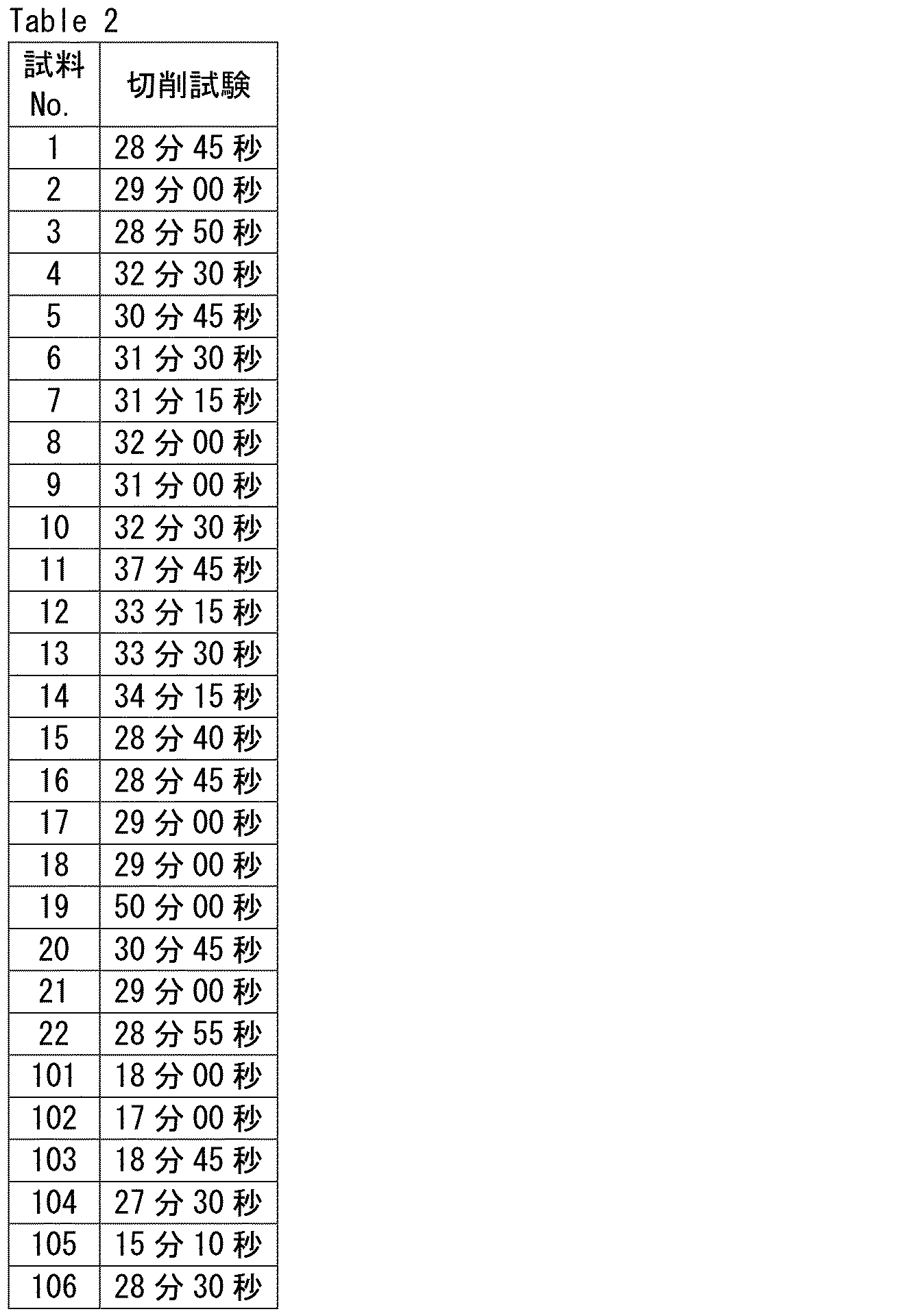
- Cutting tools Samples 1 to 22 correspond to examples, and cutting tools Samples 101 to 106 correspond to comparative examples. The results of the cutting tests confirmed that cutting tools Samples 1 to 22 have a longer tool life, even in environments with high thermal loads, than cutting tools Samples 101 to 106.
Landscapes
- Chemical & Material Sciences (AREA)
- Engineering & Computer Science (AREA)
- Mechanical Engineering (AREA)
- Chemical Kinetics & Catalysis (AREA)
- Materials Engineering (AREA)
- Metallurgy (AREA)
- Organic Chemistry (AREA)
- Inorganic Chemistry (AREA)
- General Chemical & Material Sciences (AREA)
- Physical Vapour Deposition (AREA)
- Cutting Tools, Boring Holders, And Turrets (AREA)
Abstract
Description
基材と、前記基材上に配置された被膜と、を備える切削工具であって、
前記被膜は、六方晶W(C1-aNa)xからなる第1層を含み、
前記aは、0.3以上0.8以下であり、
前記xは、0.8以上1.2以下である、切削工具である。
チタン合金の旋削加工時のように、熱負荷の高い環境下においても、長い工具寿命を有する切削工具が求められている。
本開示の切削工具は、特にチタン合金の旋削加工時のような熱負荷の高い環境下においても、長い工具寿命を有することができる。
最初に本開示の実施態様を列記して説明する。
基材と、前記基材上に配置された被膜と、を備える切削工具であって、
前記被膜は、六方晶W(C1-aNa)xからなる第1層を含み、
前記aは、0.3以上0.8以下であり、
前記xは、0.8以上1.2以下である、切削工具である。
前記被膜は、前記第1層の前記基材と反対側に設けられる第2層を更に含み、
前記第2層は、周期表4族元素、5族元素、6族元素、アルミニウムおよび珪素からなる第1群より選ばれる少なくとも1種の元素、または、前記第1群より選ばれる少なくとも1種の元素と、炭素、窒素、酸素および硼素からなる第2群より選ばれる少なくとも1種の元素とからなる化合物からなることができる。
前記被膜は、前記基材と、前記第1層との間に配置される第3層を更に含み、
前記第3層は、周期表4族元素、5族元素、6族元素、アルミニウムおよび珪素からなる第1群より選ばれる少なくとも1種の元素、または、前記第1群より選ばれる少なくとも1種の元素と、炭素、窒素、酸素および硼素からなる第2群より選ばれる少なくとも1種の元素とからなる化合物からなることができる。
前記基材は、超硬合金、サーメット、高速度鋼、セラミックス、立方晶窒化硼素焼結体およびダイヤモンド焼結体からなる群より選ばれる少なくとも1種を含むことができる。これによると、工具は高温における硬度と強度とに優れる。
本開示の一実施形態(以下、「本実施形態」とも記す。)の切削工具の具体例を、以下に図面を参照しつつ説明する。本開示の図面において、同一の参照符号は、同一部分または相当部分を表すものである。また、長さ、幅、厚さ、深さなどの寸法関係は図面の明瞭化と簡略化のために適宜変更されており、必ずしも実際の寸法関係を表すものではない。
本開示の一実施形態に係る切削工具について、図1~図4を用いて説明する。
図2に示されるように、本開示の一実施形態(以下、「実施形態1」とも記す。)に係る切削工具10は、
基材11と、基材11上に配置された被膜14と、を備える切削工具であって、
前記被膜は、六方晶W(C1-aNa)xからなる第1層12を含み、
前記aは、0.3以上0.8以下であり、
前記xは、0.8以上1.2以下である、切削工具である。
本実施形態の切削工具は、例えば、ドリル、エンドミル、ドリル用刃先交換型切削チップ、エンドミル用刃先交換型切削チップ、フライス加工用刃先交換型切削チップ、旋削加工用刃先交換型切削チップ、メタルソー、歯切工具、リーマ、タップ等であり得る。
本実施形態の基材は、この種の基材として従来公知のものであればいずれのものも使用することができる。例えば、基材は、超硬合金(例えば、炭化タングステン(WC)基超硬合金、WCの他にCoを含む超硬合金、WCの他にCr、Ti、Ta、Nb等の炭窒化物を添加した超硬合金等)、サーメット(TiC、TiN、TiCN等を主成分とするもの)、高速度鋼、セラミックス(炭化チタン、炭化珪素、窒化珪素、窒化アルミニウム、酸化アルミニウム等)、立方晶型窒化硼素焼結体(cBN焼結体)およびダイヤモンド焼結体からなる群より選ばれる少なくとも1種を含むことが好ましく、超硬合金、サーメットおよびcBN焼結体からなる群より選ばれる少なくとも1種を含むことがより好ましい。
本実施形態に係る「被膜」は、基材の少なくとも一部(例えば、切削加工時に被削材と接する切削に関与する部分)を被覆することで、切削工具における耐欠損性、耐摩耗性等の諸特性を向上させる作用を有するものである。被膜は、少なくとも切削に関与する部分を被覆することができる。被膜は、基材の全面を被覆してもよい。被膜の構成が部分的に異なっていたとしても本実施形態の範囲を逸脱するものではない。基材の切削に関与する部分とは、例えば、基材の表面において、刃先稜線からの距離が50μm以内である領域を意味する。被膜は、基材の切削に関与する部分の全面を被覆してもよい。本開示の切削工具が奏する効果を損なわない限り、基材の切削に関与する部分の一部に被膜が形成されていなくても、本実施形態の範囲を逸脱するものではない。
被膜は、六方晶W(C1-aNa)x(ここで、aは、0.3以上0.8以下であり、xは、0.8以上1.2以下である。)からなる第1層を含む。六方晶W(C1-aNa)xとは、六方晶型の結晶構造であるW(C1-aNa)xを意味する。第1層の結晶構造が六方晶型であることにより、被膜と被削材との拡散反応が抑制され、被削材の凝着が少なくなり、工具寿命が向上する。第1層は、被膜の耐熱性、耐酸化性および耐摩耗性を向上することができる。
第1層が六方晶型の結晶構造であるW(C1-aNa)xからなることは、XRD測定で分析することにより確認することができる。具体的には、各試料の基材と反対側の表面にX線を照射することにより、第1層の任意の領域に対してX線回折測定(XRD測定)を行い分析する。得られたXRDスペクトルにおいて、JCPDS(ICDD)カード01-076-7103に示されるピークおよび01―77-2001に示されるピークの両方が観察され、かつ、JCPDS(ICDD)カード01-075-1012に示されるピークおよび00―042-0853に示されるピークの両方が観察されない場合、第1層は六方晶型の結晶構造であるW(C1-aNa)xからなることが確認される。
(XRD測定条件)
走査軸 :2θ-θ
X線源 :Cu-Kα線(1.541862Å)
検出器 :0次元検出器(シンチレーションカウンタ)
管電圧 :45kV
管電流 :40mA
入射光学系 :ミラーの利用
受光光学系 :アナライザ結晶(PW3098/27)の利用
ステップ :0.03°
積算時間 :2秒
スキャン範囲(2θ) :10°~120°
第1層は、六方晶W(C1-aNa)xからなり、aは、0.3以上0.8以下であり、xは、0.8以上1.2以下である。
上記第1層の厚みの下限は、0.2μm以上とすることができる。これによると、第1層と被削材との拡散反応が抑制される。第1層の厚みの下限は、0.3μm以上でもよく、0.5μm以上でもよく、0.7μm以上でもよく、0.9μm以上でもよい。第1層の厚みの上限は、5.0μm以下とすることができる。これによると、被膜が高い硬度を有し、耐摩耗性が良好である。第1層の厚みの上限は、4.0μm以下でもよく、2.0μm以下でもよく、1.5μm以下でもよい。第1層の厚みは、0.2μm以上5.0μm以下でもよく、0.3μm以上4.0μm以下でもよく、0.5μm以上2.0μm以下でもよく、0.7μm以上1.5μm以下でもよい。
図3および図4に示されるように、被膜14は、第1層12の基材11と反対側に設けられる第2層13を更に含むことができる。ここで「第1層の基材と反対側に設けられる」とは、第1層12の上側(基材から離れる側)に第2層13が設けられていればよく、第1層12と第2層13とが互いに接触していることを要しない。言い換えると、第1層12と、第2層13との間に他の層が設けられていてもよい。第2層13は、第1層12の直上に設けられていてもよい。第2層13は、最外層であってもよい。
図4に示されるように、被膜14は、基材11と、第1層12との間に配置される第3層15を更に含むことができる。これによって、基材11と被膜14との密着性を高めることができる。
被膜は、第2層と第1層との間、または第1層と第3層との間に配置される中間層を含むことができる。中間層としては、例えばTiAlCeN、AlTiN、AlTiBN、AlTiSiN、AlTiYN、AlTiLaN、等が挙げられる。中間層の厚みは、0.1μm以上2μm以下でもよく、0.3μm以上1.5μm以下でもよく、0.4μm以上1.0μm以下でもよい。
実施形態1の切削工具の製造方法の一例について以下に説明する。本実施形態に係る切削工具の製造方法は、基材を準備する第1工程と、基材上に被膜を形成する第2工程とを備える。第2工程は、第1層を形成する工程を含む。以下、各工程について説明する。
第1工程では、基材を準備する。基材は、実施形態1に記載の基材を用いることができる。
第2工程では、基材上に被膜を形成する。第2工程は、第1層を形成する工程を含む。第1層を形成する方法としては、例えば、物理蒸着法(PVD法)が挙げられる。
[試料1~試料22、試料101~試料105]
<第1工程>
第1工程では、JIS規格K10超硬(形状:JIS規格CNMG120408)を基材として準備した。次に、上記基材をアークイオンプレーティング装置(株式会社神戸製鋼所製、商品名:AIP)の所定の位置にセットした。
第2工程では、アークイオンプレーティング法により基材の上に、第1層を含む被膜を形成して各試料の切削工具を得た。第1層の形成は、以下の方法で行った。まずWCターゲット(組成がWCを93質量%以上含むバインダレスWCであって、C量が3~6.1質量%である焼結ターゲット)を装置内の対向する2機のアーク式蒸発源にセットした。基材温度を400~550℃および装置内のガス圧を1.5~5.5Paに設定した。
試料1と同一の基材を準備し、基材上に、特許文献1の試料15と同一の方法で被膜を形成して、試料106の切削工具を得た。
各試料の切削工具について、第1層の結晶構造および第1ピークの有無、第1層の組成、各層の厚みを評価した。
各試料の第1層の結晶構造をXRDで特定した。具体的な測定方法は、実施形態1に記載されているため、その説明は繰り返さない。結果を表1の「第1層」の「結晶構造」欄に示す。
各試料の第1層の組成を電子エネルギー損失分光法(TEM-EELS)およびラザフォード後方散乱(RBS)法を用いて測定した。第2層および第3層が形成されている場合は、これらの組成も測定した。具体的な測定方法は、実施形態1に記載されているため、その説明は繰り返さない。結果を表1の「第1層(W(C1-aNa)x)」の「a」および「x」欄、「第2層」の「組成」欄および「第3層」の「組成」欄に示す。
第1層、第2層および第3層および被膜の厚みを透過型電子顕微鏡(TEM)(日本電子株式会社製、商品名:JEM-2100F)を用いて測定した。具体的な測定方法は、実施形態1に記載されているため、その説明は繰り返さない。結果を表1の各層の「厚み」欄に示す。

各試料の切削工具を用いて、以下の切削条件により切削工具が欠損するまで、または、逃げ面摩耗量が0.15mmとなるまでの切削時間(工具寿命)を測定した。結果を表2の「切削試験」の「工具寿命」欄に示す。
被削材(材質):Ti-6Al-4V
速度 :V70m/min
送り :0.2mm/rev
切り込み :1mm
上記の切削条件は、チタン合金の旋削加工に該当し、加工時に切削工具に高い熱負荷がかかる。
Claims (6)
- 基材と、前記基材上に配置された被膜と、を備える切削工具であって、
前記被膜は、六方晶W(C1-aNa)xからなる第1層を含み、
前記aは、0.3以上0.8以下であり、
前記xは、0.8以上1.2以下である、切削工具。 - 前記第1層のX線回折スペクトルにおいて、回折角度2θが46.0°以上47.0°以下の範囲にピークが存在する、請求項1に記載の切削工具。
- 前記第1層の平均厚みは、0.3μm以上4.0μm以下である、請求項1または請求項2に記載の切削工具。
- 前記被膜は、前記第1層の前記基材と反対側に設けられる第2層を更に含み、
前記第2層は、周期表4族元素、5族元素、6族元素、アルミニウムおよび珪素からなる第1群より選ばれる少なくとも1種の元素、または、前記第1群より選ばれる少なくとも1種の元素と、炭素、窒素、酸素および硼素からなる第2群より選ばれる少なくとも1種の元素とからなる化合物からなる、請求項1から請求項3のいずれか1項に記載の切削工具。 - 前記被膜は、前記基材と、前記第1層との間に配置される第3層を更に含み、
前記第3層は、周期表4族元素、5族元素、6族元素、アルミニウムおよび珪素からなる第1群より選ばれる少なくとも1種の元素、または、前記第1群より選ばれる少なくとも1種の元素と、炭素、窒素、酸素および硼素からなる第2群より選ばれる少なくとも1種の元素とからなる化合物からなる、請求項1から請求項4のいずれか1項に記載の切削工具。 - 前記基材は、超硬合金、サーメット、高速度鋼、セラミックス、立方晶窒化硼素焼結体およびダイヤモンド焼結体からなる群より選ばれる少なくとも1種を含む、請求項1から請求項5のいずれか1項に記載の切削工具。
Priority Applications (5)
| Application Number | Priority Date | Filing Date | Title |
|---|---|---|---|
| US18/577,284 US12350743B2 (en) | 2023-05-17 | 2023-05-17 | Cutting tool |
| PCT/JP2023/018429 WO2024236768A1 (ja) | 2023-05-17 | 2023-05-17 | 切削工具 |
| EP23937510.8A EP4644021A4 (en) | 2023-05-17 | 2023-05-17 | CUTTING TOOL |
| CN202380093878.1A CN120603665A (zh) | 2023-05-17 | 2023-05-17 | 切削工具 |
| JP2023565262A JP7544294B1 (ja) | 2023-05-17 | 2023-05-17 | 切削工具 |
Applications Claiming Priority (1)
| Application Number | Priority Date | Filing Date | Title |
|---|---|---|---|
| PCT/JP2023/018429 WO2024236768A1 (ja) | 2023-05-17 | 2023-05-17 | 切削工具 |
Publications (1)
| Publication Number | Publication Date |
|---|---|
| WO2024236768A1 true WO2024236768A1 (ja) | 2024-11-21 |
Family
ID=92588347
Family Applications (1)
| Application Number | Title | Priority Date | Filing Date |
|---|---|---|---|
| PCT/JP2023/018429 Ceased WO2024236768A1 (ja) | 2023-05-17 | 2023-05-17 | 切削工具 |
Country Status (5)
| Country | Link |
|---|---|
| US (1) | US12350743B2 (ja) |
| EP (1) | EP4644021A4 (ja) |
| JP (1) | JP7544294B1 (ja) |
| CN (1) | CN120603665A (ja) |
| WO (1) | WO2024236768A1 (ja) |
Cited By (2)
| Publication number | Priority date | Publication date | Assignee | Title |
|---|---|---|---|---|
| JP2024519616A (ja) * | 2021-05-07 | 2024-05-20 | エービー サンドビック コロマント | 切削工具 |
| JP2024519615A (ja) * | 2021-05-07 | 2024-05-20 | エービー サンドビック コロマント | 切削工具 |
Families Citing this family (1)
| Publication number | Priority date | Publication date | Assignee | Title |
|---|---|---|---|---|
| CN120099455B (zh) * | 2025-05-08 | 2025-07-18 | 赣州澳克泰工具技术有限公司 | 一种复合涂层刀具及其制备方法和应用 |
Citations (7)
| Publication number | Priority date | Publication date | Assignee | Title |
|---|---|---|---|---|
| JPH06262405A (ja) * | 1993-03-05 | 1994-09-20 | Toshiba Tungaloy Co Ltd | 工具用被覆部品 |
| JP2009155721A (ja) * | 2007-12-03 | 2009-07-16 | Kobe Steel Ltd | 摺動性に優れる硬質皮膜とその硬質皮膜の形成方法 |
| JP2009275293A (ja) * | 2009-08-27 | 2009-11-26 | Kobe Steel Ltd | 硬質皮膜およびその形成方法 |
| JP2010017791A (ja) * | 2008-07-09 | 2010-01-28 | Mitsubishi Materials Corp | ダイヤモンド被覆超硬合金製切削工具 |
| JP2010174375A (ja) * | 2010-02-04 | 2010-08-12 | Kobe Steel Ltd | 硬質皮膜および硬質皮膜形成用スパッタリングターゲット材 |
| WO2019181742A1 (ja) * | 2018-03-19 | 2019-09-26 | 住友電気工業株式会社 | 表面被覆切削工具 |
| JP2022095116A (ja) | 2020-12-16 | 2022-06-28 | 住友電工ハードメタル株式会社 | 切削工具 |
Family Cites Families (4)
| Publication number | Priority date | Publication date | Assignee | Title |
|---|---|---|---|---|
| JP3448840B2 (ja) * | 1997-07-18 | 2003-09-22 | 宏爾 林 | 炭窒化タングステン及びその製造方法 |
| US9896767B2 (en) * | 2013-08-16 | 2018-02-20 | Kennametal Inc | Low stress hard coatings and applications thereof |
| EP4144465B1 (en) * | 2020-12-16 | 2024-04-10 | Sumitomo Electric Hardmetal Corp. | Coated cutting tool with a layer made of tungsten metal and hexagonal di-tungsten carbide |
| CN119384329A (zh) * | 2023-05-17 | 2025-01-28 | 住友电气工业株式会社 | 切削工具 |
-
2023
- 2023-05-17 US US18/577,284 patent/US12350743B2/en active Active
- 2023-05-17 CN CN202380093878.1A patent/CN120603665A/zh active Pending
- 2023-05-17 EP EP23937510.8A patent/EP4644021A4/en active Pending
- 2023-05-17 WO PCT/JP2023/018429 patent/WO2024236768A1/ja not_active Ceased
- 2023-05-17 JP JP2023565262A patent/JP7544294B1/ja active Active
Patent Citations (7)
| Publication number | Priority date | Publication date | Assignee | Title |
|---|---|---|---|---|
| JPH06262405A (ja) * | 1993-03-05 | 1994-09-20 | Toshiba Tungaloy Co Ltd | 工具用被覆部品 |
| JP2009155721A (ja) * | 2007-12-03 | 2009-07-16 | Kobe Steel Ltd | 摺動性に優れる硬質皮膜とその硬質皮膜の形成方法 |
| JP2010017791A (ja) * | 2008-07-09 | 2010-01-28 | Mitsubishi Materials Corp | ダイヤモンド被覆超硬合金製切削工具 |
| JP2009275293A (ja) * | 2009-08-27 | 2009-11-26 | Kobe Steel Ltd | 硬質皮膜およびその形成方法 |
| JP2010174375A (ja) * | 2010-02-04 | 2010-08-12 | Kobe Steel Ltd | 硬質皮膜および硬質皮膜形成用スパッタリングターゲット材 |
| WO2019181742A1 (ja) * | 2018-03-19 | 2019-09-26 | 住友電気工業株式会社 | 表面被覆切削工具 |
| JP2022095116A (ja) | 2020-12-16 | 2022-06-28 | 住友電工ハードメタル株式会社 | 切削工具 |
Non-Patent Citations (1)
| Title |
|---|
| See also references of EP4644021A1 |
Cited By (2)
| Publication number | Priority date | Publication date | Assignee | Title |
|---|---|---|---|---|
| JP2024519616A (ja) * | 2021-05-07 | 2024-05-20 | エービー サンドビック コロマント | 切削工具 |
| JP2024519615A (ja) * | 2021-05-07 | 2024-05-20 | エービー サンドビック コロマント | 切削工具 |
Also Published As
| Publication number | Publication date |
|---|---|
| US12350743B2 (en) | 2025-07-08 |
| EP4644021A1 (en) | 2025-11-05 |
| US20240383045A1 (en) | 2024-11-21 |
| JPWO2024236768A1 (ja) | 2024-11-21 |
| EP4644021A4 (en) | 2026-02-25 |
| JP7544294B1 (ja) | 2024-09-03 |
| CN120603665A (zh) | 2025-09-05 |
Similar Documents
| Publication | Publication Date | Title |
|---|---|---|
| JP7544294B1 (ja) | 切削工具 | |
| JP7354933B2 (ja) | 切削工具 | |
| JP7622344B2 (ja) | 切削工具 | |
| JP7574906B2 (ja) | 切削工具 | |
| WO2022176057A1 (ja) | 切削工具 | |
| JP7119279B1 (ja) | 切削工具 | |
| JP7067691B1 (ja) | 切削工具 | |
| US12090557B1 (en) | Cutting tool | |
| JP7443655B2 (ja) | 切削工具 | |
| JP7251347B2 (ja) | 表面被覆切削工具 | |
| JP7704313B1 (ja) | 切削工具 | |
| JP7708333B1 (ja) | 切削工具 | |
| JP7704312B1 (ja) | 切削工具 | |
| JP7708332B1 (ja) | 切削工具 | |
| US12186812B2 (en) | Cutting tool | |
| WO2022244191A1 (ja) | 切削工具 | |
| WO2022244190A1 (ja) | 切削工具 |
Legal Events
| Date | Code | Title | Description |
|---|---|---|---|
| WWE | Wipo information: entry into national phase |
Ref document number: 2023565262 Country of ref document: JP |
|
| 121 | Ep: the epo has been informed by wipo that ep was designated in this application |
Ref document number: 23937510 Country of ref document: EP Kind code of ref document: A1 |
|
| WWG | Wipo information: grant in national office |
Ref document number: 18577284 Country of ref document: US |
|
| WWE | Wipo information: entry into national phase |
Ref document number: 2023937510 Country of ref document: EP |
|
| ENP | Entry into the national phase |
Ref document number: 2023937510 Country of ref document: EP Effective date: 20250729 |
|
| ENP | Entry into the national phase |
Ref document number: 2023937510 Country of ref document: EP Effective date: 20250729 |
|
| WWE | Wipo information: entry into national phase |
Ref document number: 202380093878.1 Country of ref document: CN |
|
| WWP | Wipo information: published in national office |
Ref document number: 202380093878.1 Country of ref document: CN |
|
| WWP | Wipo information: published in national office |
Ref document number: 2023937510 Country of ref document: EP |
|
| NENP | Non-entry into the national phase |
Ref country code: DE |