WO2024241981A1 - レンズユニット、灯具及びLiDAR装置 - Google Patents
レンズユニット、灯具及びLiDAR装置 Download PDFInfo
- Publication number
- WO2024241981A1 WO2024241981A1 PCT/JP2024/017847 JP2024017847W WO2024241981A1 WO 2024241981 A1 WO2024241981 A1 WO 2024241981A1 JP 2024017847 W JP2024017847 W JP 2024017847W WO 2024241981 A1 WO2024241981 A1 WO 2024241981A1
- Authority
- WO
- WIPO (PCT)
- Prior art keywords
- light
- metalens
- lens unit
- incident
- nanostructure
- Prior art date
- Legal status (The legal status is an assumption and is not a legal conclusion. Google has not performed a legal analysis and makes no representation as to the accuracy of the status listed.)
- Ceased
Links
Images


Classifications
-
- F—MECHANICAL ENGINEERING; LIGHTING; HEATING; WEAPONS; BLASTING
- F21—LIGHTING
- F21S—NON-PORTABLE LIGHTING DEVICES; SYSTEMS THEREOF; VEHICLE LIGHTING DEVICES SPECIALLY ADAPTED FOR VEHICLE EXTERIORS
- F21S41/00—Illuminating devices specially adapted for vehicle exteriors, e.g. headlamps
- F21S41/20—Illuminating devices specially adapted for vehicle exteriors, e.g. headlamps characterised by refractors, transparent cover plates, light guides or filters
- F21S41/25—Projection lenses
- F21S41/275—Lens surfaces, e.g. coatings or surface structures
-
- F—MECHANICAL ENGINEERING; LIGHTING; HEATING; WEAPONS; BLASTING
- F21—LIGHTING
- F21S—NON-PORTABLE LIGHTING DEVICES; SYSTEMS THEREOF; VEHICLE LIGHTING DEVICES SPECIALLY ADAPTED FOR VEHICLE EXTERIORS
- F21S41/00—Illuminating devices specially adapted for vehicle exteriors, e.g. headlamps
- F21S41/20—Illuminating devices specially adapted for vehicle exteriors, e.g. headlamps characterised by refractors, transparent cover plates, light guides or filters
- F21S41/29—Attachment thereof
- F21S41/295—Attachment thereof specially adapted to projection lenses
-
- F—MECHANICAL ENGINEERING; LIGHTING; HEATING; WEAPONS; BLASTING
- F21—LIGHTING
- F21V—FUNCTIONAL FEATURES OR DETAILS OF LIGHTING DEVICES OR SYSTEMS THEREOF; STRUCTURAL COMBINATIONS OF LIGHTING DEVICES WITH OTHER ARTICLES, NOT OTHERWISE PROVIDED FOR
- F21V13/00—Producing particular characteristics or distribution of the light emitted by means of a combination of elements specified in two or more of main groups F21V1/00 - F21V11/00
- F21V13/02—Combinations of only two kinds of elements
-
- F—MECHANICAL ENGINEERING; LIGHTING; HEATING; WEAPONS; BLASTING
- F21—LIGHTING
- F21V—FUNCTIONAL FEATURES OR DETAILS OF LIGHTING DEVICES OR SYSTEMS THEREOF; STRUCTURAL COMBINATIONS OF LIGHTING DEVICES WITH OTHER ARTICLES, NOT OTHERWISE PROVIDED FOR
- F21V5/00—Refractors for light sources
-
- F—MECHANICAL ENGINEERING; LIGHTING; HEATING; WEAPONS; BLASTING
- F21—LIGHTING
- F21V—FUNCTIONAL FEATURES OR DETAILS OF LIGHTING DEVICES OR SYSTEMS THEREOF; STRUCTURAL COMBINATIONS OF LIGHTING DEVICES WITH OTHER ARTICLES, NOT OTHERWISE PROVIDED FOR
- F21V5/00—Refractors for light sources
- F21V5/04—Refractors for light sources of lens shape
-
- G—PHYSICS
- G01—MEASURING; TESTING
- G01S—RADIO DIRECTION-FINDING; RADIO NAVIGATION; DETERMINING DISTANCE OR VELOCITY BY USE OF RADIO WAVES; LOCATING OR PRESENCE-DETECTING BY USE OF THE REFLECTION OR RERADIATION OF RADIO WAVES; ANALOGOUS ARRANGEMENTS USING OTHER WAVES
- G01S17/00—Systems using the reflection or reradiation of electromagnetic waves other than radio waves, e.g. lidar systems
- G01S17/88—Lidar systems specially adapted for specific applications
- G01S17/93—Lidar systems specially adapted for specific applications for anti-collision purposes
- G01S17/931—Lidar systems specially adapted for specific applications for anti-collision purposes of land vehicles
-
- G—PHYSICS
- G01—MEASURING; TESTING
- G01S—RADIO DIRECTION-FINDING; RADIO NAVIGATION; DETERMINING DISTANCE OR VELOCITY BY USE OF RADIO WAVES; LOCATING OR PRESENCE-DETECTING BY USE OF THE REFLECTION OR RERADIATION OF RADIO WAVES; ANALOGOUS ARRANGEMENTS USING OTHER WAVES
- G01S7/00—Details of systems according to groups G01S13/00, G01S15/00, G01S17/00
- G01S7/48—Details of systems according to groups G01S13/00, G01S15/00, G01S17/00 of systems according to group G01S17/00
- G01S7/481—Constructional features, e.g. arrangements of optical elements
- G01S7/4811—Constructional features, e.g. arrangements of optical elements common to transmitter and receiver
- G01S7/4813—Housing arrangements
-
- G—PHYSICS
- G01—MEASURING; TESTING
- G01S—RADIO DIRECTION-FINDING; RADIO NAVIGATION; DETERMINING DISTANCE OR VELOCITY BY USE OF RADIO WAVES; LOCATING OR PRESENCE-DETECTING BY USE OF THE REFLECTION OR RERADIATION OF RADIO WAVES; ANALOGOUS ARRANGEMENTS USING OTHER WAVES
- G01S7/00—Details of systems according to groups G01S13/00, G01S15/00, G01S17/00
- G01S7/48—Details of systems according to groups G01S13/00, G01S15/00, G01S17/00 of systems according to group G01S17/00
- G01S7/481—Constructional features, e.g. arrangements of optical elements
- G01S7/4814—Constructional features, e.g. arrangements of optical elements of transmitters alone
-
- G—PHYSICS
- G02—OPTICS
- G02B—OPTICAL ELEMENTS, SYSTEMS OR APPARATUS
- G02B1/00—Optical elements characterised by the material of which they are made; Optical coatings for optical elements
- G02B1/002—Optical elements characterised by the material of which they are made; Optical coatings for optical elements made of materials engineered to provide properties not available in nature, e.g. metamaterials
-
- G—PHYSICS
- G02—OPTICS
- G02B—OPTICAL ELEMENTS, SYSTEMS OR APPARATUS
- G02B13/00—Optical objectives specially designed for the purposes specified below
-
- G—PHYSICS
- G02—OPTICS
- G02B—OPTICAL ELEMENTS, SYSTEMS OR APPARATUS
- G02B3/00—Simple or compound lenses
- G02B3/02—Simple or compound lenses with non-spherical faces
- G02B3/08—Simple or compound lenses with non-spherical faces with discontinuous faces, e.g. Fresnel lens
-
- F—MECHANICAL ENGINEERING; LIGHTING; HEATING; WEAPONS; BLASTING
- F21—LIGHTING
- F21S—NON-PORTABLE LIGHTING DEVICES; SYSTEMS THEREOF; VEHICLE LIGHTING DEVICES SPECIALLY ADAPTED FOR VEHICLE EXTERIORS
- F21S41/00—Illuminating devices specially adapted for vehicle exteriors, e.g. headlamps
- F21S41/10—Illuminating devices specially adapted for vehicle exteriors, e.g. headlamps characterised by the light source
- F21S41/14—Illuminating devices specially adapted for vehicle exteriors, e.g. headlamps characterised by the light source characterised by the type of light source
- F21S41/141—Light emitting diodes [LED]
- F21S41/143—Light emitting diodes [LED] the main emission direction of the LED being parallel to the optical axis of the illuminating device
-
- F—MECHANICAL ENGINEERING; LIGHTING; HEATING; WEAPONS; BLASTING
- F21—LIGHTING
- F21Y—INDEXING SCHEME ASSOCIATED WITH SUBCLASSES F21K, F21L, F21S and F21V, RELATING TO THE FORM OR THE KIND OF THE LIGHT SOURCES OR OF THE COLOUR OF THE LIGHT EMITTED
- F21Y2103/00—Elongate light sources, e.g. fluorescent tubes
- F21Y2103/10—Elongate light sources, e.g. fluorescent tubes comprising a linear array of point-like light-generating elements
-
- F—MECHANICAL ENGINEERING; LIGHTING; HEATING; WEAPONS; BLASTING
- F21—LIGHTING
- F21Y—INDEXING SCHEME ASSOCIATED WITH SUBCLASSES F21K, F21L, F21S and F21V, RELATING TO THE FORM OR THE KIND OF THE LIGHT SOURCES OR OF THE COLOUR OF THE LIGHT EMITTED
- F21Y2115/00—Light-generating elements of semiconductor light sources
- F21Y2115/10—Light-emitting diodes [LED]
-
- F—MECHANICAL ENGINEERING; LIGHTING; HEATING; WEAPONS; BLASTING
- F21—LIGHTING
- F21Y—INDEXING SCHEME ASSOCIATED WITH SUBCLASSES F21K, F21L, F21S and F21V, RELATING TO THE FORM OR THE KIND OF THE LIGHT SOURCES OR OF THE COLOUR OF THE LIGHT EMITTED
- F21Y2115/00—Light-generating elements of semiconductor light sources
- F21Y2115/30—Semiconductor lasers
Definitions
- the present invention relates to a lens unit, a lighting fixture, and a LiDAR device.
- Lamps in which light emitted from a light source enters a projection lens are known as vehicle headlamps, such as automobile headlights.
- Patent Document 1 discloses such a vehicle headlamp.
- a convex lens is used as the projection lens of the vehicle headlamp in the following Patent Document 1. Therefore, the light from the light source is emitted with a small divergence angle by the projection lens.
- Metalens have multiple nanostructures that modulate the phase of light, and dirt such as dust easily adheres to the minute irregularities of the multiple nanostructures. In addition, it is sometimes impossible to wipe off dirt from the nanostructures because doing so may damage the nanostructures. If dirt such as dust gets into the irregularities of the nanostructures, the functionality of the metalens may deteriorate.
- the present invention aims to provide a lens unit, a lighting fixture, and a LiDAR device that can suppress deterioration of the function of the metalens.
- the lens unit of the present invention is characterized by comprising: a first metalens having a first entrance surface on which light is incident and a first exit surface from which the light incident on the first entrance surface exits, and having a plurality of first nanostructures on the first exit surface side that modulate the phase of the light; and a second metalens facing the first exit surface, having a second entrance surface on which the light exiting from the first exit surface is incident and a second exit surface from which the light incident on the second entrance surface exits, and having a plurality of second nanostructures on the second entrance surface side that modulate the phase of the light.
- This lens unit uses the first metalens and the second metalens to modulate the phase of incident light, thereby making it possible to increase the amount of change in the phase of the light compared to when there is only one metalens. Furthermore, in the lens unit, the first nanostructure of the first metalens and the second nanostructure of the second metalens are arranged facing each other. That is, the first nanostructure and the second nanostructure are arranged facing inward. Therefore, compared to when the first nanostructure and the second nanostructure face outward, the lens unit can prevent the first nanostructure and the second nanostructure from coming into contact with dirt such as dust from the outside. Thus, the lens unit can prevent dirt from adhering to the first nanostructure and the second nanostructure. Therefore, the lens unit can prevent deterioration of function.
- the lens unit includes a cover body that encloses at least a portion of the space formed between the first metalens and the second metalens.
- This configuration can block at least a portion of the boundary between the space where the first nanostructure and the second nanostructure meet and the external space. Therefore, the lens unit can more effectively prevent dirt from the external space from adhering to the first nanostructure and the second nanostructure.
- the distance between the first nanostructure and the second nanostructure facing each other is at least twice the wavelength of the light.
- the lens unit may further include a third metalens disposed between the first metalens and the second metalens, having a third entrance surface facing the first exit surface onto which the light exiting from the first exit surface is incident, and a third exit surface from which the light entering the third entrance surface is exited, and having a plurality of third nanostructures on at least one of the third entrance surface side and the third exit surface side that modulate the phase of the light, and the light exiting from the first exit surface is incident on the second entrance surface via the third metalens.
- a third metalens disposed between the first metalens and the second metalens, having a third entrance surface facing the first exit surface onto which the light exiting from the first exit surface is incident, and a third exit surface from which the light entering the third entrance surface is exited, and having a plurality of third nanostructures on at least one of the third entrance surface side and the third exit surface side that modulate the phase of the light, and the light exiting from the first exit surface is incident on the second entrance surface via
- the lens unit can increase the amount of phase change in the incident light as the light passes through the third metalens. Furthermore, the lens unit can prevent dirt from adhering to the nanostructure of the third metalens by disposing the third metalens between the first metalens and the second metalens.
- the lighting fixture of the present invention is characterized by comprising any one of the lens units described above and a light source that emits the light.
- the lighting fixture can emit light modulated by the first nanostructure and the second nanostructure. Furthermore, by using the lens unit described above, the lighting fixture can prevent dirt from adhering to the first structure and the second structure, and can prevent the function of the metalens from deteriorating.
- the lamp may also have an outer cover that transmits the light and a housing that surrounds the light source, and the lens unit may be at least a part of the outer cover.
- the lighting fixture can have the metalens installed on the outermost layer of the lighting fixture. This eliminates the need to provide a metalens inside the housing, improving design freedom by enabling the lighting fixture to be made smaller. Furthermore, even if the metalens is installed on the outermost layer of the lighting fixture, the first nanostructure and second nanostructure are not exposed to the outside, so adhesion of dirt to the first nanostructure and second nanostructure can be suppressed, and deterioration of the metalens function can be suppressed. Therefore, with this lighting fixture, changes in the light distribution pattern of the emitted light due to a deterioration in the function of the metalens can be suppressed.
- the LiDAR device of the present invention may also include a light source that emits light to an object, any of the lens units described above, and a sensor that receives light reflected from the object, and the lens unit may modulate the phase of at least one of the light and the reflected light.
- the LiDAR device can modulate the light or the reflected light using the first nanostructure and the second nanostructure. Furthermore, by using the lens unit described above, the LiDAR device can prevent dirt from adhering to the first structure and the second structure, and can suppress deterioration of the function of the metalens. Therefore, with this LiDAR device, deterioration of the object detection ability can be suppressed.
- the present invention provides a lens unit, a lighting fixture, and a LiDAR device that can suppress deterioration of the metalens' functions.
- FIG. 1 is a cross-sectional view that illustrates a vehicle headlamp according to a first embodiment of the present invention
- FIG. 2 is a cross-sectional view illustrating the lens unit illustrated in FIG. 1 .
- 2 is an enlarged cross-sectional view showing a part of the lens unit shown in FIG. 1 .
- FIG. 6 is a cross-sectional view illustrating a vehicle headlamp according to a second embodiment of the present invention.
- 5 is an enlarged cross-sectional view showing a portion of the outer cover shown in FIG. 4.
- FIG. 11 is a conceptual diagram illustrating a LiDAR device according to a third embodiment of the present invention.
- FIG. 11 is a cross-sectional view showing a first modified example of the lens unit in the embodiment of the present invention.
- FIG. 11 is a cross-sectional view showing a second modified example of the lens unit in the embodiment of the present invention.
- FIG. 11 is a cross-sectional view showing a third modified example of the lens unit in the embodiment
- the lamp according to the first embodiment is a vehicle headlamp, and emits light when attached to a vehicle.
- FIG. 1 is a diagram showing a vehicle headlamp 1 according to an embodiment of the present invention.
- FIG. 1 is a diagram showing a schematic vertical cross section of the vehicle headlamp 1.
- the direction in which light L travels is defined as the forward direction
- the direction opposite to the direction in which light L travels is defined as the rearward direction.
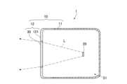
- the vehicle headlamp 1 according to this embodiment mainly comprises a housing 10, a light source 20, and a lens unit 30.
- the housing 10 constitutes the exterior of the vehicle headlamp 1.
- the housing 10 mainly comprises an external housing 11 and an outer cover 12.
- the external housing 11 is formed in a bowl shape and is open at the front.
- the outer cover 12 is fixed to the external housing 11 so as to cover the opening.
- the outer cover 12 is formed in a bowl shape and is open at the rear.
- the opening of the outer cover 12 has approximately the same shape as the opening of the external housing 11.
- the outer cover 12 transmits light L from the light source 20.
- the outer cover 12 is made of plastic or glass that transmits light L.
- a space S1 is formed by the external housing 11 and the outer cover 12.
- the light source 20 and the lens unit 30 are housed within the space S1. That is, the housing 10 surrounds the light source 20 and the lens unit 30.
- the light source 20, the lens unit 30, and the outer cover 12 are arranged side by side in the front-to-rear direction within the space S1. Furthermore, the light source 20, the lens unit 30, and the outer cover 12 are arranged in order toward the front.
- the light source 20 emits light L toward the lens unit 30.
- the light source 20 has a plurality of light-emitting elements that emit light L, and a circuit board on which the plurality of light-emitting elements are mounted.
- the plurality of light-emitting elements are arranged in a matrix, have emission surfaces for light L that are positioned on approximately the same plane, and emit light L forward.
- the light emitted from each light emitting point of each light emitting element is a spherical wave and has a predetermined divergence angle. Therefore, the light L emitted from each light emitting element propagates forward while spreading at a predetermined divergence angle.
- the amount of light L emitted by the multiple light emitting elements can be changed individually.
- the light emitting element is an LED (Light Emitting Diode) that emits white light
- the light source 20 is a so-called LED array.
- the number and configuration of the light emitting elements are not particularly limited.
- the light emitting element may be configured to include multiple LEDs that emit light of different wavelengths, or may be configured to include multiple LDs (Laser Diodes) that emit light of different wavelengths and phosphors provided on the LDs.
- the light source 20 may also be composed of a single light emitting element.
- the light source 20 having multiple light-emitting elements may be capable of emitting light L having a predetermined light distribution pattern by selecting the light-emitting element that emits the light L, and may be capable of changing the light distribution pattern by changing the selection.
- the light source 20 may also be capable of adjusting the intensity distribution of the light L in the light distribution pattern by adjusting the amount of light emitted from each light-emitting element. Note that even if the light source 20 has multiple light-emitting elements, it is not necessary that the light distribution pattern of the emitted light L can be changed.
- the lens unit 30 functions as a projection lens that reduces the divergence angle of the light L from the light source 20.
- the lens unit 30 modulates the phase of the light L from the light source 20.
- the lens unit 30 modulates the phase of the light L so as to reduce the divergence angle of the light L from the light source 20.
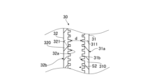
- FIG. 2 is a cross-sectional view that shows the lens unit 30 shown in FIG. 1. Like FIG. 1, FIG. 2 is a cross-sectional view that shows the vertical cross section. As shown in FIG. 2, the lens unit 30 mainly comprises a first metalens 31, a second metalens 32, and a cover body 33. FIG. 3 is an enlarged view of a portion of the first metalens 31 and the second metalens 32.
- the first metalens 31 transmits the light L from the light source 20 and modulates the phase of the light L.
- the first metalens 31 is configured to reduce the divergence angle of the light L from the light source 20.
- the first metalens 31 also has a first incident surface 31a on which the light L from the light source 20 is incident.
- the first incident surface 31a faces backward.
- the first metalens 31 also has a first exit surface 31b from which the light L incident on the first incident surface 31a exits.
- the first exit surface 31b faces forward.
- the first metalens 31 also includes a substrate 310.
- the substrate 310 is, for example, a circular member having a predetermined thickness.
- the substrate 310 is formed in a flat shape. Furthermore, the substrate 310 transmits light L.
- the material of the substrate 310 is glass, resin, or the like.
- a plurality of first nanostructures 311 that modulate the phase of light L are provided on the first emission surface 31b side of the substrate 310.
- first nanostructure 311 is labeled with a reference number, and the reference numbers of the other first nanostructures 311 are omitted.
- the plurality of first nanostructures 311 are arranged across the entire surface of the substrate 310.
- the first nanostructure 311 extends forward.
- the shape of the first nanostructure 311 is, for example, cylindrical, and the diameter is smaller than the longest wavelength of the light L emitted from the light source 20.
- the shape of the first nanostructure 311 is not particularly limited as long as the width of the first nanostructure 311 is smaller than the longest wavelength of the light L emitted from the light source 20.
- the shape of the first nanostructure 311 may be a rectangular column shape or a pyramidal shape.
- the first nanostructure 311 may be composed of a pair of square columns arranged at a predetermined interval.
- the shapes of the first nanostructures 311 may be different. Examples of materials constituting the first nanostructure 311 include glass and resin.
- the materials constituting the first nanostructure 311 and the substrate 310 may be the same or different.
- the second metalens 32 is placed in front of the first metalens 31 in the lens unit 30.
- the second metalens 32 is placed at a predetermined distance from the first metalens 31.
- the second metalens 32 modulates the phase of the light L from the first metalens 31.
- the second metalens 32 is configured to reduce the divergence angle of the light L from the first metalens 31.
- the second metalens 32 also has a second incident surface 32a on which the light L emitted from the first exit surface 31b is incident.
- the second incident surface 32a faces the first exit surface 31b.
- the second metalens 32 also has a second exit surface 32b from which the light L incident on the second incident surface 32a is emitted.
- the second exit surface 32b faces forward.
- the second metalens 32 includes a substrate 320.
- the description of the substrate 320 is similar to that of the substrate 310, and therefore will not be repeated.
- a plurality of second nanostructures 321 that modulate the phase of light L are provided on the second incident surface 32a side of the substrate 320.
- the plurality of second nanostructures 321 are arranged across the entire surface of the substrate 320.
- the second nanostructure 321 extends toward the rear. Other explanations of the second nanostructure 321 are omitted because they are similar to those of the first nanostructure 311. In addition, the second nanostructure 321 may be made of the same material or have a different shape than the first nanostructure 311.
- the second metalens 32 has a second incident surface 32a through which the light L from the first metalens 31 is incident.
- the second incident surface 32a faces rearward. That is, the second incident surface 32a faces the first exit surface 31b.
- the second exit surface 32b includes a portion of the rear surface of the substrate 320 where the second nanostructures 321 are not arranged, and the surfaces of the multiple second nanostructures 321.
- the second metalens 32 also has a second exit surface 32b through which the light L is emitted.
- the second exit surface 32b faces forward.
- a space S2 is formed between the first metalens 31 and the second metalens 32.
- a plurality of first nanostructures 311 and a plurality of second nanostructures 321 are arranged facing each other.
- the cover body 33 encloses at least a portion of the space S2.
- the cover body 33 is a ring-shaped member extending from the outer periphery of the first metalens 31 toward the outer periphery of the second metalens 32.
- the cover body 33 seals the space S2.
- the cover body 33 is made of rubber, resin, plastic, or the like.
- first nanostructures 311 and second nanostructures 321 facing each other are separated by a distance d or more.
- the distance d is at least twice the longest wavelength of the light L emitted by the light source 20.
- the respective distances between the first nanostructures 311 and second nanostructures 321 facing each other are at least twice the longest wavelength of the light L.
- the cover body 33 may be a C-shaped member extending from a part of the outer periphery of the first metalens 31 toward the part of the outer periphery of the second metalens 32 that faces the outer periphery.
- the lens unit 30 may not be provided with the cover body 33.
- the space S2 may be filled with a predetermined member that transmits the light L and has a refractive index different from the refractive indexes of the first nanostructure 311 and the second nanostructure 321.
- the space S2 may be filled with a resin that transmits the light L.
- the light source 20 emits light L using power supplied from an external source.
- the light L emitted from the light source 20 is incident on the first incident surface 31a of the first metalens 31 with a predetermined divergence angle.
- the light M incident on the first incident surface 31a is modulated by the multiple first nanostructures 311 so that the divergence angle becomes smaller.
- the light L modulated by the multiple first nanostructures 311 is emitted from the first exit surface 31b and is incident on the second incident surface 32a of the second metalens 32.
- Light M incident on the second entrance surface 32a is modulated by the multiple second nanostructures 321 so that the divergence angle becomes smaller.
- Light L modulated by the multiple second nanostructures 321 is emitted from the second exit surface 32b.
- Light L emitted from the second exit surface 32b passes through the outer cover 12 and is emitted to the outside.
- the vehicle headlamp 1 configured as described above emits light L from the light source 20 to the outside through the lens unit 30. Therefore, the vehicle headlamp 1 can increase the amount of change in the phase of the light L by modulating the light L using the first metalens 31 and the second metalens 32.
- the cover body 33 covers at least a portion of the space S2 formed by the first metalens 31 and the second metalens 32. Furthermore, the first nanostructure 311 of the first metalens 31 and the second nanostructure 321 of the second metalens 32 are disposed inside the space S2. Therefore, the cover body 33 of the lens unit 30 can prevent dirt such as dust from the outside from coming into contact with the first nanostructure 311 and the second nanostructure 321. Therefore, the lens unit 30 can prevent dirt from adhering to the first nanostructure 311 and the second nanostructure 321, and can suppress deterioration of the functions of the first metalens 31 and the second metalens 32.
- the vehicle headlamp 1 may further include a lens such as a convex lens.
- the vehicle headlamp 1 may include a primary lens between the light source 20 and the lens unit 30.
- the vehicle headlamp 1 may also include a lens between the lens unit 30 and the outer cover 12.
- the vehicle headlamp 1 may also include multiple lens units 30.
- FIG. 4 is a diagram showing a vehicle headlamp 1 according to an embodiment of the present invention.
- FIG. 4 is a diagram showing a schematic vertical cross section of the vehicle headlamp 1.
- FIG. 5 is an enlarged cross section of a portion of the outer cover 12 according to this embodiment.
- the vehicle headlamp 1 according to this embodiment mainly comprises a housing 10 and a light source 20.
- the points that differ from the first embodiment will be described.
- the outer cover 12 mainly comprises a lens unit 30 and a cover member 121.
- the cover member 121 is formed in a bowl shape and is open at the rear.
- the rear opening of the cover member 121 has approximately the same shape as the opening of the external housing 11.
- the front of the cover member 121 is also open.
- the front opening of the cover member 121 is formed in the center of the outer cover 12 when the outer cover 12 is viewed from the front.
- the cover member 121 may or may not transmit light L.
- a lens unit 30 is fixed to the front opening of the cover member 121 so as to cover the opening.
- the lens unit 30 is configured as at least a part of the outer cover 12.
- the lens unit 30 is positioned so as to overlap at least a part of the area illuminated by the light L from the light source 20.
- the lens unit 30 does not include a cover body 33.
- the outer periphery of the first metalens 31 and the outer periphery of the second metalens 32 are in contact with and fixed to the cover member 121. That is, the cover member 121 surrounds the space S2 formed between the first metalens 31 and the second metalens 32. Therefore, the cover member 121 also serves as a cover body that surrounds the space S2.
- the light source 20 emits light L using power supplied from an external source.
- the light L emitted from the light source 20 is incident on the first incident surface 31a of the first metalens 31 with a predetermined divergence angle.
- the light L incident on the first incident surface 31a is modulated by the multiple first nanostructures 311 so that the divergence angle becomes smaller.
- the light L modulated by the multiple first nanostructures 311 is emitted from the first exit surface 31b and is incident on the second incident surface 32a of the second metalens 32.
- the light L incident on the second incident surface 32a is modulated by the multiple second nanostructures 321 so that the divergence angle becomes smaller.
- the light L modulated by the multiple second nanostructures 321 is emitted to the outside.
- the vehicle headlamp 1 of this embodiment includes the lens unit 30 as part of the outer cover 12. Therefore, the lens unit 30 is used as the outermost layer of the lamp. Therefore, the lens unit 30 can include other components inside and the external housing 11 can be made smaller, improving design freedom.
- the lens unit 30 can prevent dirt from adhering to the first nanostructure 311 and the second nanostructure 321. Therefore, the lens unit 30 can prevent deterioration of the functions of the first metalens 31 and the second metalens 32.
- the vehicle headlamp 1 may also include a primary lens between the light source 20 and the lens unit 30.
- the lens unit 30 may also be fixed to the opening of the external housing 11.
- FIG. 6 is a diagram showing a schematic example of the configuration of the LiDAR device 2 according to this embodiment.
- the direction from the LiDAR device 2 toward the target A is defined as the forward direction
- the direction opposite to the forward direction is defined as the rearward direction.
- the LiDAR device 2 measures the distance between itself and each point on the target A.
- the LiDAR device 2 emits light to the target A, receives the reflected light from the target A, and measures the distance between itself and each point on the target A based on the time between emitting the light and receiving the reflected light.
- the LiDAR device 2 mainly comprises a lens unit 30, a light source 40, a lens unit 50, a sensor 60, a control device 70, and a bandpass filter 80.
- the light source 40 and the lens unit 50 are arranged in a line facing forward.
- the sensor 60, the lens unit 30, and the bandpass filter 80 are also arranged in a line facing forward.
- the control device 70 is communicatively connected to the light source 40 and the sensor 60 via a signal line or the like.
- the light source 40 emits light M towards the lens unit 50 in accordance with a control signal from the control device 70.
- the light source 40 emits laser light having a predetermined divergence angle as the light M.
- the light source 40 emits a flash as the light M.
- the light source 40 includes an LD that emits light M.
- the light source 40 may also include a surface-emitting VCSEL (Vertical Cavity Surface Emitting Laser).
- the lens unit 50 is disposed in front of the light source 40.
- the lens unit 50 modulates the phase of the light M from the light source 40 so as to reduce the divergence angle of the light M from the light source 40.
- the lens unit 50 modulates the phase of the light M so that the light M becomes parallel light.
- the configuration of the lens unit 50 is generally similar to the configuration of the lens unit 30 according to the first embodiment, so a description of the lens unit 50 is omitted.
- the first nanostructure 311 and the second nanostructure 321 provided in the lens unit 50 may be similar to or different from the first nanostructure 311 and the second nanostructure 321 according to the first embodiment.
- Bandpass filter 80 transmits light with a predetermined range of wavelengths including the wavelength of light M and blocks other light, thereby extracting reflected light R from light N from object A.
- bandpass filter 80 includes a dielectric multilayer film.
- the lens unit 30 modulates the phase of the reflected light R from the bandpass filter 80 so as to focus the reflected light R on the sensor 60.
- the first nanostructure 311 and the second nanostructure 321 of the lens unit 30 may be the same as or different from the first nanostructure 311 and the second nanostructure 321 of the first embodiment or the first nanostructure 311 and the second nanostructure 321 of the lens unit 50.
- the sensor 60 converts the reflected light R focused by the lens unit 30 into an electrical signal as an image of a predetermined resolution. That is, the sensor 60 converts the reflected light R from the lens unit 30 into an electrical signal in a plurality of elements corresponding to the predetermined resolution.
- the sensor 60 transmits the electrical signal converted from the reflected light R to the control device 70 via a signal line or the like.
- the sensor 60 includes a CCD (Charge Coupled Device), a CMOS (Complementary Metal-Oxide-Semiconductor), an APD (Avalanche Photodiode), or a SPAD (Single Photon Avalanche Diode), etc.
- the control device 70 may be, for example, a microcontroller, an integrated circuit such as an IC (Integrated Circuit), an LSI (Large-scale Integrated Circuit), or an ASIC (Application Specific Integrated Circuit), or a Numerical Control (NC) device.
- the control device 70 operates by executing a program.
- the control device 70 transmits a control signal to the light source 40 to emit light M in accordance with operations by the user, etc.
- the light source 40 emits light M in accordance with the control signal from the control device 70.
- the light M emitted from the light source 40 passes through the lens unit 50 and is emitted toward the target A.
- bandpass filter 80 When light M is emitted to object A and reflected by object A, light N including reflected light R is incident on bandpass filter 80. In bandpass filter 80, reflected light R is extracted from light N, and the extracted reflected light R is incident on lens unit 30. Reflected light R incident on lens unit 30 is focused on sensor 60. Sensor 60 converts the focused reflected light R into an electrical signal and transmits it to control device 70.
- the control device 70 calculates the distance between each point of the object A and the LiDAR device 2 from the electrical signal from the sensor 60 according to a predetermined algorithm.
- the control device 70 may store data indicating the calculated distance in an internal memory or the like, or may transmit the data to an external device.
- the LiDAR device 2 configured as described above modulates light M using the lens unit 50 and emits it to the target A. Therefore, the LiDAR device 2 can increase the amount of change in the phase of light M by modulating light M using the first metalens 31 and the second metalens 32.
- the LiDAR device 2 modulates the reflected light R using the lens unit 30. Therefore, the LiDAR device 2 can increase the amount of change in the phase of the reflected light R by modulating the reflected light R using the first metalens 31 and the second metalens 32.
- the lens units 30 and 50 can suppress the adhesion of dirt to the first metalens 31 and the second metalens 32, respectively, and suppress deterioration of the functions of the first metalens 31 and the second metalens 32. Therefore, the LiDAR device 2 can suppress the adhesion of dirt to the first nanostructure 311 and the second nanostructure 321 while using metalenses to modulate the light M and the reflected light R. Therefore, the LiDAR device 2 can suppress deterioration of the functions of the first metalens 31 and the second metalens 32.
- the bandpass filter 80 provided in the LiDAR device 2 may be disposed between the lens unit 30 and the sensor 60. Also, the LiDAR device 2 does not need to be provided with a bandpass filter 80. In this case, the sensor 60 may convert light of a predetermined range of wavelengths, including the wavelength of the light M, into an electrical signal.
- one of the lens unit 50 and the lens unit 30 may be composed of a lens such as a convex lens.
- the LiDAR device 2 may further include a lens in front of or behind the lens unit 30.
- the LiDAR device 2 may further include a lens in front of or behind the lens unit 50.
- the LiDAR device 2 may also measure the distance to the object A by scanning light M.
- light N including reflected light R of the scanned light M may be incident on the bandpass filter 80.
- FIG. 7 is a cross-sectional view that shows a schematic view of the lens unit 30 according to this modified example.
- FIG. 7 is a diagram that shows a schematic view of a vertical cross section of the lens unit 30.
- the lens unit 30 mainly includes a first metalens 31, a second metalens 32, a cover body 33, and a third metalens 34.
- the third metalens 34 is installed in the space S2 at a predetermined distance from the first metalens 31 and the second metalens 32.
- the third metalens 34 modulates the phase of the light L from the light source 20.
- the third metalens 34 is configured to reduce the divergence angle of the light L from the first metalens 31.
- the third metalens 34 also has a third entrance surface 34a on which the light L emitted from the first exit surface 31b is incident.
- the third entrance surface 34a faces the first exit surface 31b.
- the third metalens 34 also has a third exit surface 34b on which the light L incident on the third entrance surface 34a is emitted.
- the third exit surface 34b faces the second entrance surface 32a.
- the third metalens 34 includes a substrate 340.
- the description of the substrate 340 is similar to that of the substrate 310, and therefore will not be repeated.
- a plurality of third nanostructures 341 that modulate the phase of light L are provided on the third exit surface 34b side of the substrate 340.
- the plurality of third nanostructures 341 are arranged across the entire surface of the substrate 340.
- the description of the third nanostructure 341 is omitted here because it is similar to the description of the first nanostructure 311. Furthermore, the third nanostructure 341 may be made of the same material or have the same shape as the first nanostructure 311 or the second nanostructure 321, or may be different.
- the third nanostructure 341 and the second nanostructure 321 facing each other are separated by a distance d or more.
- the distance between the third nanostructure 341 and the second nanostructure 321 facing each other is at least twice the longest wavelength of the light L.
- each first nanostructure 311 is spaced a distance d from the third incident surface 34a.
- the distance between each of the multiple first nanostructures 311 and the third incident surface 34a is at least twice the longest wavelength of the light L.
- the light L emitted from the first exit surface 31b of the first metalens 31 is incident on the third entrance surface 34a of the third metalens 34.
- the light L incident on the third entrance surface 34a is modulated by the plurality of third nanostructures 341.
- the light L modulated by the plurality of third nanostructures 341 is emitted from the third exit surface 34b and is incident on the second entrance surface 32a of the second metalens 32. That is, the light L emitted from the first exit surface 31b is incident on the second entrance surface 32a of the second metalens 32 via the third metalens 34.
- the lens unit 30 configured as described above includes a third metalens 34 between the first metalens 31 and the second metalens 32.
- the light L from the light source 20 passes through the first metalens 31, the third metalens 34, and the second metalens 32. Therefore, the light L from the light source 20 is also modulated by the third metalens 34.
- the lens unit 30 can increase the amount of change in the phase of the light L.
- the lens unit 30 also includes a third metalens 34 in the space S2. Therefore, the lens unit 30 can prevent external dirt such as dust from coming into contact with the third nanostructure 341 of the third metalens 34. Thus, the lens unit 30 can prevent dirt from adhering to the third nanostructure 341, and can prevent deterioration of the function of the third metalens 34.
- FIG. 8 is a cross-sectional view that shows a lens unit 30 according to this modified example.
- FIG. 8 shows a cross-section of the lens unit 30 in the vertical direction.
- a plurality of third nanostructures 342 that modulate the phase of light L are provided on the third exit surface 34b side of the substrate 340.
- the plurality of third nanostructures 342 are arranged across the entire surface of the substrate 340.
- the third nanostructure 342 extends toward the rear. Other explanations of the third nanostructure 342 are omitted because they are similar to those of the first nanostructure 311. Furthermore, the third nanostructure 342 may be of the same material or shape as the first nanostructure 311, the second nanostructure 321, or the third nanostructure 341, or may be different.
- the third nanostructure 342 and the first nanostructure 311 facing each other are separated by a distance d or more.
- the distance between the third nanostructure 342 and the first nanostructure 311 facing each other is at least twice the longest wavelength of the light L.
- each second nanostructure 321 is spaced a distance d from the third exit surface 34b.
- the distance between each of the second nanostructures 321 and the third exit surface 34b is at least twice the longest wavelength of the light L.
- the light L emitted from the first exit surface 31b of the first metalens 31 is incident on the third entrance surface 34a of the third metalens 34.
- the light L incident on the third entrance surface 34a is modulated by the plurality of third nanostructures 342.
- the light L modulated by the plurality of third nanostructures 342 is emitted from the third exit surface 34b and is incident on the second entrance surface 32a of the second metalens 32. That is, the light L emitted from the first exit surface 31b is incident on the second entrance surface 32a of the second metalens 32 via the third metalens 34.
- a third modified example of the lens unit 30 will be described. Note that components that are the same as or equivalent to those in the first embodiment will be given the same reference numerals and will not be described again unless otherwise specified.
- This modified example differs from the first modified example in that the configuration of the third metalens 34 is different.
- the lens unit 30 according to this modified example may be used in place of the lens unit 30 in the first or second embodiment. In addition, in the second embodiment, the lens unit 30 does not need to include the cover body 33. In addition, the lens unit 30 according to this modified example may be used in place of at least one of the lens unit 30 or the lens unit 50 in the third embodiment.
- FIG. 9 is a cross-sectional view that shows a lens unit 30 according to this modified example.
- FIG. 9 shows a cross-section of the lens unit 30 in the vertical direction.
- a plurality of third nanostructures 341 are provided on the third exit surface 34b side of the third metalens 34.
- the reference numbers of the other third nanostructures 341 are omitted.
- third nanostructures 342 are provided on the third entrance surface 34a side of the third metalens 34.
- third nanostructures 342 are labeled with a reference number, and the reference numbers of the other third nanostructures 342 are omitted.
- the light L emitted from the first exit surface 31b of the first metalens 31 is incident on the third entrance surface 34a of the third metalens 34.
- the light L incident on the third entrance surface 34a is modulated by the plurality of third nanostructures 341 and 342.
- the light L modulated by the plurality of third nanostructures 341 and 342 is emitted from the third exit surface 34b and is incident on the second entrance surface 32a of the second metalens 32. That is, the light L emitted from the first exit surface 31b is incident on the second entrance surface 32a of the second metalens 32 via the third metalens 34.
- the vehicle headlamp 1 is a headlamp, but this is not particularly limited.
- the vehicle headlamp 1 may be configured to irradiate an illuminated object such as a road surface with light that constitutes an image.
- the direction of the light emitted by the vehicle headlamp 1 and the position at which the vehicle headlamp 1 is attached to the vehicle are not particularly limited.
- the color of the light emitted by the vehicle headlamp 1 is not limited to a specific color.
- the lens unit 30 that reduces the divergence angle of the light L from the light source 20 has been described as an example.
- the lens unit 30 may be configured to increase the divergence angle of the light L from the light source 20.
- the substrates 310 and 320 are formed on a flat surface.
- the substrates 310 and 320 may be curved.
- the lens unit 30 in which the third metalens 34 is disposed between the first metalens 31 and the second metalens 32 has been described as an example.
- the lens unit 30 may include multiple metalenses between the first metalens 31 and the second metalens 32.
- the lens unit 30 may include a convex lens or a concave lens between the first metalens 31 and the second metalens 32.
- the lens units 30 according to the first, second and third modified examples may be used in place of the lens unit 30 in the first or second embodiment. Furthermore, when the lens units 30 according to the first, second and third modified examples are used in the second embodiment, the lens units 30 do not need to be provided with the cover body 33. Furthermore, the lens units 30 according to the first, second and third modified examples may be used in place of at least one of the lens units 30 or the lens units 50 in the third embodiment.
- the present invention provides a lens unit, a lamp, and a LiDAR device that can suppress deterioration of the metalens' functions, and can be used in fields such as headlights for vehicles such as automobiles, and measuring devices for measuring distances.
Landscapes
- Engineering & Computer Science (AREA)
- Physics & Mathematics (AREA)
- General Physics & Mathematics (AREA)
- General Engineering & Computer Science (AREA)
- Optics & Photonics (AREA)
- Computer Networks & Wireless Communication (AREA)
- Radar, Positioning & Navigation (AREA)
- Remote Sensing (AREA)
- Electromagnetism (AREA)
- Non-Portable Lighting Devices Or Systems Thereof (AREA)
Abstract
Description
第1実施形態に係る灯具は、車両用前照灯であり、車両に取り付けられた状態で光を出射する。
次に、本発明の第2実施形態について詳細に説明する。なお、第1実施形態と同一又は同等の構成要素については、同一の参照符号を付して特に説明する場合を除き重複する説明は省略する。本実施形態では、レンズユニット30がアウターカバー12の少なくとも一部として構成される点が第1実施形態と異なる。
次に、本発明の第3実施形態について詳細に説明する。なお、第1実施形態と同一又は同等の構成要素については、同一の参照符号を付して特に説明する場合を除き重複する説明は省略する。本実施形態では、レンズユニット30がLiDAR(Light Detection And Ranging)装置に用いられる点が第1実施形態と異なる。
次に、レンズユニット30の第1変形例について説明する。なお、第1実施形態と同一又は同等の構成要素については、同一の参照符号を付して特に説明する場合を除き重複する説明は省略する。本変形例では、レンズユニット30がさらにメタレンズを備える点が第1実施形態と異なる。図7は、本変形例に係るレンズユニット30を概略的に示す断面図である。図7は、レンズユニット30の鉛直方向の断面を概略的に示す図である。図7が示すように、即ち、レンズユニット30は、第1メタレンズ31と、第2メタレンズ32と、カバー体33と、第3メタレンズ34と、を主な構成として備える。
次に、レンズユニット30の第2変形例について説明する。なお、第1実施形態と同一又は同等の構成要素については、同一の参照符号を付して特に説明する場合を除き重複する説明は省略する。本変形例では、第3メタレンズ34の構成が異なる点が第1変形例と異なる。
次に、レンズユニット30の第3変形例について説明する。なお、第1実施形態と同一又は同等の構成要素については、同一の参照符号を付して特に説明する場合を除き重複する説明は省略する。本変形例では、第3メタレンズ34の構成が異なる点が第1変形例と異なる。本変形例に係るレンズユニット30は、第1又は第2実施形態におけるレンズユニット30の代わりに用いられてもよい。また、第2実施形態においては、レンズユニット30は、カバー体33を備えなくともよい。また、本変形例に係るレンズユニット30は、第3実施形態においてレンズユニット30又はレンズユニット50の少なくとも1つの代わりに用いられてもよい。
Claims (7)
- 光が入射する第1入射面及び前記第1入射面に入射する前記光が出射する第1出射面を有し、前記第1出射面側に前記光の位相を変調する複数の第1ナノ構造体が設けられる第1メタレンズと、
前記第1出射面に対向し前記第1出射面から出射する前記光が入射する第2入射面及び前記第2入射面に入射する前記光が出射する第2出射面を有し、前記第2入射面側に前記光の位相を変調する複数の第2ナノ構造体が設けられる第2メタレンズと、
を備える
ことを特徴とするレンズユニット。 - 前記第1メタレンズと前記第2メタレンズとの間に形成される空間の少なくとも一部を囲うカバー体を備える
ことを特徴とする請求項1に記載のレンズユニット。 - 互いに向かい合う前記第1ナノ構造体と前記第2ナノ構造体との間の各距離は、前記光の波長の2倍以上である
ことを特徴とする請求項1に記載のレンズユニット。 - 前記第1メタレンズと前記第2メタレンズとの間に配置され、前記第1出射面に対向し前記第1出射面から出射する前記光が入射する第3入射面及び前記第3入射面に入射する前記光が出射する第3出射面を有し、前記第3入射面側及び前記第3出射面側の少なくとも一方に前記光の位相を変調する複数の第3ナノ構造体が設けられる第3メタレンズを備え、
前記第2入射面には、前記第3メタレンズを介して、前記第1出射面から出射する前記光が入射する
ことを特徴する請求項1に記載のレンズユニット。 - 請求項1から4のいずれか1項に記載のレンズユニットと、
前記光を出射する光源と、
を備える
ことを特徴とする灯具。 - 前記光を透過するアウターカバーを有し、前記光源を囲う筐体を備え、
前記レンズユニットは、前記アウターカバーの少なくとも一部である
ことを特徴とする請求項5に記載の灯具。 - 対象物に光を出射する光源と、
請求項1から4のいずれか1項に記載のレンズユニットと、
前記光が前記対象物で反射した反射光を受光するセンサと、
を備え、
前記レンズユニットは、前記光及び前記反射光の少なくとも一方の位相を変調する
ことを特徴とするLiDAR装置。
Priority Applications (3)
| Application Number | Priority Date | Filing Date | Title |
|---|---|---|---|
| CN202480034267.4A CN121175597A (zh) | 2023-05-25 | 2024-05-14 | 透镜单元、灯具以及LiDAR装置 |
| JP2025522340A JPWO2024241981A1 (ja) | 2023-05-25 | 2024-05-14 | |
| EP24810988.6A EP4722768A4 (en) | 2023-05-25 | 2024-05-14 | LENS UNIT, LAMP AND LIDAR DEVICE |
Applications Claiming Priority (2)
| Application Number | Priority Date | Filing Date | Title |
|---|---|---|---|
| JP2023086496 | 2023-05-25 | ||
| JP2023-086496 | 2023-05-25 |
Publications (1)
| Publication Number | Publication Date |
|---|---|
| WO2024241981A1 true WO2024241981A1 (ja) | 2024-11-28 |
Family
ID=93589822
Family Applications (1)
| Application Number | Title | Priority Date | Filing Date |
|---|---|---|---|
| PCT/JP2024/017847 Ceased WO2024241981A1 (ja) | 2023-05-25 | 2024-05-14 | レンズユニット、灯具及びLiDAR装置 |
Country Status (4)
| Country | Link |
|---|---|
| EP (1) | EP4722768A4 (ja) |
| JP (1) | JPWO2024241981A1 (ja) |
| CN (1) | CN121175597A (ja) |
| WO (1) | WO2024241981A1 (ja) |
Citations (5)
| Publication number | Priority date | Publication date | Assignee | Title |
|---|---|---|---|---|
| US20180095257A1 (en) * | 2016-10-04 | 2018-04-05 | Samsung Electronics Co., Ltd. | Rotational varifocal planar lens |
| JP2019015970A (ja) * | 2017-07-10 | 2019-01-31 | 三星電子株式会社Samsung Electronics Co.,Ltd. | ビームスキャニング装置、及びそれを含む光学装置 |
| US20200355913A1 (en) * | 2019-05-07 | 2020-11-12 | Samsung Electronics Co., Ltd. | Metalens and optical apparatus including the same |
| WO2021172169A1 (ja) | 2020-02-26 | 2021-09-02 | 株式会社小糸製作所 | 車両用前照灯 |
| WO2022025031A1 (ja) * | 2020-07-31 | 2022-02-03 | 株式会社小糸製作所 | 車両用灯具 |
Family Cites Families (8)
| Publication number | Priority date | Publication date | Assignee | Title |
|---|---|---|---|---|
| JP2012237580A (ja) * | 2011-05-10 | 2012-12-06 | Honda Motor Co Ltd | 車両のレーザーレーダーユニット |
| EP3226042B1 (en) * | 2016-03-30 | 2022-05-04 | Samsung Electronics Co., Ltd. | Structured light generator and object recognition apparatus including the same |
| JP7461294B2 (ja) * | 2017-08-31 | 2024-04-03 | メタレンズ,インコーポレイテッド | 透過型メタサーフェスレンズ統合 |
| KR102444288B1 (ko) * | 2017-11-08 | 2022-09-16 | 삼성전자주식회사 | 메타 렌즈를 포함하는 프로젝터 |
| WO2022102856A1 (ko) * | 2020-11-12 | 2022-05-19 | 주식회사 에스오에스랩 | 라이다 장치 |
| DE102021112717A1 (de) * | 2021-05-17 | 2022-11-17 | HELLA GmbH & Co. KGaA | Beleuchtungsvorrichtung für Fahrzeuge |
| CN114545370A (zh) * | 2022-02-25 | 2022-05-27 | 深圳迈塔兰斯科技有限公司 | 激光雷达发射系统及其对应的接收系统 |
| CN216896898U (zh) * | 2022-03-03 | 2022-07-05 | 深圳迈塔兰斯科技有限公司 | 基于超透镜的汽车投影灯 |
-
2024
- 2024-05-14 EP EP24810988.6A patent/EP4722768A4/en active Pending
- 2024-05-14 CN CN202480034267.4A patent/CN121175597A/zh active Pending
- 2024-05-14 WO PCT/JP2024/017847 patent/WO2024241981A1/ja not_active Ceased
- 2024-05-14 JP JP2025522340A patent/JPWO2024241981A1/ja active Pending
Patent Citations (5)
| Publication number | Priority date | Publication date | Assignee | Title |
|---|---|---|---|---|
| US20180095257A1 (en) * | 2016-10-04 | 2018-04-05 | Samsung Electronics Co., Ltd. | Rotational varifocal planar lens |
| JP2019015970A (ja) * | 2017-07-10 | 2019-01-31 | 三星電子株式会社Samsung Electronics Co.,Ltd. | ビームスキャニング装置、及びそれを含む光学装置 |
| US20200355913A1 (en) * | 2019-05-07 | 2020-11-12 | Samsung Electronics Co., Ltd. | Metalens and optical apparatus including the same |
| WO2021172169A1 (ja) | 2020-02-26 | 2021-09-02 | 株式会社小糸製作所 | 車両用前照灯 |
| WO2022025031A1 (ja) * | 2020-07-31 | 2022-02-03 | 株式会社小糸製作所 | 車両用灯具 |
Non-Patent Citations (1)
| Title |
|---|
| See also references of EP4722768A4 |
Also Published As
| Publication number | Publication date |
|---|---|
| JPWO2024241981A1 (ja) | 2024-11-28 |
| EP4722768A1 (en) | 2026-04-08 |
| CN121175597A (zh) | 2025-12-19 |
| EP4722768A4 (en) | 2026-04-08 |
Similar Documents
| Publication | Publication Date | Title |
|---|---|---|
| EP3339919B1 (en) | Vehicle lighting apparatus | |
| CN110094692B (zh) | 集成LiDAR系统的照明装置及汽车 | |
| KR20190033006A (ko) | 차량용 등기구 | |
| US11713858B2 (en) | Vehicle lighting | |
| US11371670B2 (en) | Lamp for automobile and automobile including the lamp | |
| US20250052397A1 (en) | Automotive lighting device and automotive vehicle | |
| KR102481310B1 (ko) | 자동차 헤드램프용 조명 장치 | |
| EP4201740A1 (en) | Automotive lighting device and automotive vehicle | |
| EP4202495A1 (en) | Automotive lighting device and automotive vehicle | |
| WO2023118159A1 (en) | Automotive lighting arrangement and automotive vehicle | |
| US12422119B2 (en) | LED module for vehicle headlight and vehicle headlight with such LED module | |
| EP3943808B1 (en) | Lighting tool for vehicle | |
| FR2906345A1 (fr) | Phare de vehicule a distribution de lumiere optimisee | |
| US20240422410A1 (en) | Light source unit and vehicle | |
| WO2024241981A1 (ja) | レンズユニット、灯具及びLiDAR装置 | |
| JP2014037195A (ja) | 照明制御システム、制御装置、および照明装置 | |
| KR101822259B1 (ko) | 차량용 조명 장치 | |
| EP1498311A2 (en) | Infrared projector | |
| JP2019016512A (ja) | 車両用灯具 | |
| JP2006510523A (ja) | 多機能照明装置 | |
| KR20250058451A (ko) | 차량용 램프 및 이를 포함하는 차량 | |
| WO2018216547A1 (ja) | 車両用灯具 | |
| CN210801005U (zh) | 车辆用灯具 | |
| CN116235002B (zh) | 用于车辆前灯的照明模块 | |
| WO2024085150A1 (ja) | 車両用前照灯 |
Legal Events
| Date | Code | Title | Description |
|---|---|---|---|
| 121 | Ep: the epo has been informed by wipo that ep was designated in this application |
Ref document number: 24810988 Country of ref document: EP Kind code of ref document: A1 |
|
| ENP | Entry into the national phase |
Ref document number: 2025522340 Country of ref document: JP Kind code of ref document: A |
|
| NENP | Non-entry into the national phase |
Ref country code: DE |
|
| WWE | Wipo information: entry into national phase |
Ref document number: 2024810988 Country of ref document: EP |
|
| ENP | Entry into the national phase |
Ref document number: 2024810988 Country of ref document: EP Effective date: 20260102 |
|
| ENP | Entry into the national phase |
Ref document number: 2024810988 Country of ref document: EP Effective date: 20260102 |
|
| ENP | Entry into the national phase |
Ref document number: 2024810988 Country of ref document: EP Effective date: 20260102 |
|
| ENP | Entry into the national phase |
Ref document number: 2024810988 Country of ref document: EP Effective date: 20260102 |
|
| ENP | Entry into the national phase |
Ref document number: 2024810988 Country of ref document: EP Effective date: 20260102 |
|
| ENP | Entry into the national phase |
Ref document number: 2024810988 Country of ref document: EP Effective date: 20260102 |
|
| WWP | Wipo information: published in national office |
Ref document number: 2024810988 Country of ref document: EP |